KR20140072131A - Flexible touch sensor with fine pitch interconnect - Google Patents
Flexible touch sensor with fine pitch interconnect Download PDFInfo
- Publication number
- KR20140072131A KR20140072131A KR1020147011169A KR20147011169A KR20140072131A KR 20140072131 A KR20140072131 A KR 20140072131A KR 1020147011169 A KR1020147011169 A KR 1020147011169A KR 20147011169 A KR20147011169 A KR 20147011169A KR 20140072131 A KR20140072131 A KR 20140072131A
- Authority
- KR
- South Korea
- Prior art keywords
- conductive layer
- layer
- transparent conductive
- transparent
- metallic
- Prior art date
Links
Images


Classifications
-
- G—PHYSICS
- G06—COMPUTING; CALCULATING OR COUNTING
- G06F—ELECTRIC DIGITAL DATA PROCESSING
- G06F3/00—Input arrangements for transferring data to be processed into a form capable of being handled by the computer; Output arrangements for transferring data from processing unit to output unit, e.g. interface arrangements
- G06F3/01—Input arrangements or combined input and output arrangements for interaction between user and computer
- G06F3/03—Arrangements for converting the position or the displacement of a member into a coded form
- G06F3/041—Digitisers, e.g. for touch screens or touch pads, characterised by the transducing means
- G06F3/044—Digitisers, e.g. for touch screens or touch pads, characterised by the transducing means by capacitive means
- G06F3/0445—Digitisers, e.g. for touch screens or touch pads, characterised by the transducing means by capacitive means using two or more layers of sensing electrodes, e.g. using two layers of electrodes separated by a dielectric layer
-
- G—PHYSICS
- G06—COMPUTING; CALCULATING OR COUNTING
- G06F—ELECTRIC DIGITAL DATA PROCESSING
- G06F3/00—Input arrangements for transferring data to be processed into a form capable of being handled by the computer; Output arrangements for transferring data from processing unit to output unit, e.g. interface arrangements
- G06F3/01—Input arrangements or combined input and output arrangements for interaction between user and computer
- G06F3/03—Arrangements for converting the position or the displacement of a member into a coded form
- G06F3/041—Digitisers, e.g. for touch screens or touch pads, characterised by the transducing means
- G06F3/044—Digitisers, e.g. for touch screens or touch pads, characterised by the transducing means by capacitive means
- G06F3/0446—Digitisers, e.g. for touch screens or touch pads, characterised by the transducing means by capacitive means using a grid-like structure of electrodes in at least two directions, e.g. using row and column electrodes
-
- H—ELECTRICITY
- H05—ELECTRIC TECHNIQUES NOT OTHERWISE PROVIDED FOR
- H05K—PRINTED CIRCUITS; CASINGS OR CONSTRUCTIONAL DETAILS OF ELECTRIC APPARATUS; MANUFACTURE OF ASSEMBLAGES OF ELECTRICAL COMPONENTS
- H05K1/00—Printed circuits
- H05K1/02—Details
- H05K1/0274—Optical details, e.g. printed circuits comprising integral optical means
-
- H—ELECTRICITY
- H05—ELECTRIC TECHNIQUES NOT OTHERWISE PROVIDED FOR
- H05K—PRINTED CIRCUITS; CASINGS OR CONSTRUCTIONAL DETAILS OF ELECTRIC APPARATUS; MANUFACTURE OF ASSEMBLAGES OF ELECTRICAL COMPONENTS
- H05K3/00—Apparatus or processes for manufacturing printed circuits
- H05K3/02—Apparatus or processes for manufacturing printed circuits in which the conductive material is applied to the surface of the insulating support and is thereafter removed from such areas of the surface which are not intended for current conducting or shielding
- H05K3/06—Apparatus or processes for manufacturing printed circuits in which the conductive material is applied to the surface of the insulating support and is thereafter removed from such areas of the surface which are not intended for current conducting or shielding the conductive material being removed chemically or electrolytically, e.g. by photo-etch process
-
- G—PHYSICS
- G06—COMPUTING; CALCULATING OR COUNTING
- G06F—ELECTRIC DIGITAL DATA PROCESSING
- G06F2203/00—Indexing scheme relating to G06F3/00 - G06F3/048
- G06F2203/041—Indexing scheme relating to G06F3/041 - G06F3/045
- G06F2203/04102—Flexible digitiser, i.e. constructional details for allowing the whole digitising part of a device to be flexed or rolled like a sheet of paper
-
- H—ELECTRICITY
- H05—ELECTRIC TECHNIQUES NOT OTHERWISE PROVIDED FOR
- H05K—PRINTED CIRCUITS; CASINGS OR CONSTRUCTIONAL DETAILS OF ELECTRIC APPARATUS; MANUFACTURE OF ASSEMBLAGES OF ELECTRICAL COMPONENTS
- H05K1/00—Printed circuits
- H05K1/02—Details
- H05K1/09—Use of materials for the conductive, e.g. metallic pattern
-
- H—ELECTRICITY
- H05—ELECTRIC TECHNIQUES NOT OTHERWISE PROVIDED FOR
- H05K—PRINTED CIRCUITS; CASINGS OR CONSTRUCTIONAL DETAILS OF ELECTRIC APPARATUS; MANUFACTURE OF ASSEMBLAGES OF ELECTRICAL COMPONENTS
- H05K2201/00—Indexing scheme relating to printed circuits covered by H05K1/00
- H05K2201/03—Conductive materials
- H05K2201/0302—Properties and characteristics in general
-
- H—ELECTRICITY
- H05—ELECTRIC TECHNIQUES NOT OTHERWISE PROVIDED FOR
- H05K—PRINTED CIRCUITS; CASINGS OR CONSTRUCTIONAL DETAILS OF ELECTRIC APPARATUS; MANUFACTURE OF ASSEMBLAGES OF ELECTRICAL COMPONENTS
- H05K2201/00—Indexing scheme relating to printed circuits covered by H05K1/00
- H05K2201/03—Conductive materials
- H05K2201/032—Materials
Abstract
용품은, 예를 들어, 터치 센서와 같이, 반대 방향의 두 측면을 갖고, 중심 중합체 UV 투명 기판, 상기 중합체 기판의 반대 방향의 두 주표면 상의 투명 도전층, 각 투명 도전층 상의 금속성 도전층, 및 각 금속성 도전층 상의 패터닝된 포토이미지 마스크를 포함하는 다층 구조를 포함한다.The article has two sides in opposite directions, such as, for example, a touch sensor, and has a central polymer UV transparent substrate, a transparent conductive layer on two main surfaces in the opposite direction of the polymer substrate, a metallic conductive layer on each transparent conductive layer, And a multi-layer structure comprising a patterned photoimage mask on each metallic conductive layer.
Description
터치 감지 디바이스는 점점 더 사용자가 통상적으로 태블릿, 터치 폰, 및 기타 상업적 터치 상호작용형 시스템을 포함하는 전자 시스템과 상호작용하는 보편적인 방법이 되었다. 터치 감지 디바이스는 기계식 버튼, 키패드, 키보드 및 포인팅 디바이스에 대한 필요성을 줄이거나 제거함으로써 사용자가 전자 시스템 및 디스플레이와 편리하게 인터페이스하는 것을 가능하게 한다. 예를 들어, 사용자는 아이콘에 의해 식별되는 위치에서 온-디스플레이 터치 스크린(on-display touch screen)을 간단히 터치함으로써 복잡한 일련의 명령어를 수행할 수 있다.Touch sensing devices have become a universal way for more and more users to interact with electronic systems, typically including tablets, touch phones, and other commercial touch interactive systems. Touch sensing devices enable users to conveniently interface with electronic systems and displays by reducing or eliminating the need for mechanical buttons, keypads, keyboards, and pointing devices. For example, the user can perform a complex series of commands by simply touching the on-display touch screen at the location identified by the icon.
예를 들어, 저항, 적외선, 용량성, 표면 탄성파, 전자기, 근접장 이미징 등을 포함하는 터치 감지 디바이스를 구현하기 위한 몇 가지 유형의 기술들이 있다. 용량성 터치 감지 디바이스는 다수의 응용에서 잘 동작하는 것으로 알려져 있다. 많은 터치 감지 디바이스에서, 센서 내의 전도성 물체가 사용자의 손가락과 같은 전도성 터치 도구에 용량적으로 결합될 때 입력이 감지된다. 일반적으로, 2개의 전기 전도성 부재가 실제로 터치하는 일 없이 서로 근접하게 될 때마다, 이들 사이에 정전용량이 형성된다. 용량성 터치 감지 디바이스의 경우, 손가락과 같은 물체가 터치 감지 표면에 접근함에 따라, 작은 정전용량이 물체와 이 물체에 아주 근접한 감지 지점 사이에 형성된다. 감지 지점들 각각에서의 정전용량의 변화를 검출하고 감지 지점의 위치에 주목함으로써, 감지 회로는 다수의 물체를 인식할 수 있고 물체가 터치 표면을 가로질러 이동함에 따라 이 물체의 특성을 판정할 수 있다.There are several types of techniques for implementing touch sensing devices including, for example, resistance, infrared, capacitive, surface acoustic wave, electromagnetic, near field imaging, and the like. Capacitive touch sensing devices are known to work well in many applications. In many touch sensing devices, the input is sensed when a conductive object in the sensor is capacitively coupled to a conductive touch tool, such as a user's finger. Generally, whenever two electrically conductive members are brought close to each other without actually touching them, a capacitance is formed therebetween. In the case of a capacitive touch sensing device, as an object such as a finger approaches the touch sensitive surface, a small capacitance is formed between the object and a sensing point very close to the object. By sensing the change in capacitance at each of the sensing points and noting the position of the sensing point, the sensing circuit can recognize a number of objects and determine the characteristics of the object as it moves across the touch surface have.
용량성 터치 감지 디바이스는 종종 감지 요소로서 패터닝된 투명 도전체 층들을 포함한다. 패터닝된 투명 도전체는 종종 행과 열 형태의 길고, 좁은 투명 도전성 전극의 어레이를 포함한다. 도전성 금속 패턴을 제공함으로써 제어기와 투명 전극 사이에 전기 접촉부가 형성된다. 공지된 방법에서는, 가요성 인쇄 회로(FPC)가 이방성 도전성 필름(ACF) 결합을 이용하여 투명 도전체의 후미 부분에 직접 결합된다. 다른 공지된 방법에서는, 도전성 금속 패턴과 결합 패드가 인쇄 방법으로 각각의 투명 전극에 제공된다. 예를 들어, 투명 전극의 후미 부분 상에 도전성 트레이스를 만들기 위하여 도전성 잉크가 투명 전도체 상에 도포되고 가열된다.Capacitive touch sensing devices often include patterned transparent conductive layers as sensing elements. The patterned transparent conductor includes an array of long, narrow transparent conductive electrodes, often in rows and columns. By providing a conductive metal pattern, an electrical contact is formed between the controller and the transparent electrode. In a known method, a flexible printed circuit (FPC) is directly bonded to the trailing portion of the transparent conductor using anisotropic conductive film (ACF) bonding. In another known method, a conductive metal pattern and a bonding pad are provided for each transparent electrode by a printing method. For example, a conductive ink is applied and heated on the transparent conductor to make a conductive trace on the trailing portion of the transparent electrode.
FPC 및 ACF 결합 공정은 고비용이고 높은 사이클 시간을 수반한다. 도전성 잉크 인쇄 방법은 도전성 잉크 인쇄 공정에 의한 미세 피치를 제공하는 데 있어서 제약때문에 센서에 넓은 비-감지 영역을 필요로 한다. 또한, 가열 온도가 올라갈수록 예를 들어 인듐 주석 산화물(ITO)의 균열(crack) 및 베이스 필름의 탁해짐과 같은 신뢰성 문제를 유발한다.FPC and ACF bonding processes are costly and involve high cycle times. The conductive ink printing method requires a wide non-sensing area in the sensor due to its limitations in providing fine pitch by the conductive ink printing process. In addition, the higher the heating temperature, the more reliability problems such as cracking of indium tin oxide (ITO) and turbidity of the base film are caused.
매트릭스 유형의 센서를 얻기 위하여, 행 전극 및 열 전극은 광학적 투명 접착제를 이용하여 직교 방향으로 라미네이트된다. 행 전극 및 열 전극 사이에 정교한 정열이 중요하며, 그렇지 않을 경우 수율이 떨어질 수 있다. 또한, 라미네이트 공정 중 거품 및 에어 갭(air gap)의 형성을 피할 수 없다. 광학적 투명 접착제 및 베이스 폴리에스테르 필름을 모두 구비하는 행 전극 및 열 전극 층은 센서를 두껍게 만들 수 있다.To obtain a matrix type of sensor, the row and column electrodes are laminated in an orthogonal direction using an optically transparent adhesive. Elaborate alignment between the row and column electrodes is important, otherwise the yield may drop. Also, the formation of bubbles and air gaps during the lamination process can not be avoided. A row electrode and a column electrode layer, both with an optical transparent adhesive and a base polyester film, can thicken the sensor.
일 양태에서, 본 발명은, 예를 들어, 터치 센서와 같이, 반대 방향의 두 측면을 갖고, 반대 방향의 두 주표면을 갖는 중심 중합체 UV 투명 기판, 상기 중합체 기판의 반대 방향의 두 주표면 상의 투명 도전층, 각 투명 도전층 상의 금속성 도전층을 포함하는 다층 구조를 제공하는 단계; 투명 도전층을 위한 원하는 패턴을 갖는 포토이미지 마스크를 형성하기 위하여 두 금속성 도전층 상에 제1 포토이미지(photoimage) 층을 도포하고 패터닝하는 단계; 금속성 도전층 및 투명 도전층 중에서 포토이미지 마스크에 의해 노출된 부분을 에칭하는 단계; 포토이미지 마스크를 제거하는 단계; 금속성 도전층을 위한 원하는 패턴을 갖는 포토이미지 마스크를 형성하기 위하여 각 금속성 도전층의 남은 부분 위에 제2 포토이미지 층을 도포하고 패터닝하는 단계; 및 금속성 도전층의 노출된 부분을 에칭하는 단계를 포함하는 방법을 제공한다.In one aspect, the present invention provides a process for producing a polymeric UV transparent substrate, such as, for example, a touch sensor, comprising a central polymer UV transparent substrate having two opposite sides and having two main surfaces in opposite directions, Providing a multilayer structure comprising a transparent conductive layer and a metallic conductive layer on each transparent conductive layer; Applying and patterning a first photoimage layer on the two metallic conductive layers to form a photoimage mask having a desired pattern for the transparent conductive layer; Etching the exposed portions of the metallic conductive layer and the transparent conductive layer by a photoimage mask; Removing the photo image mask; Applying and patterning a second photoimage layer over a remaining portion of each metallic conductive layer to form a photoimage mask having a desired pattern for the metallic conductive layer; And etching the exposed portions of the metallic conductive layer.
다른 양태에서, 본 발명은, 예를 들어, 터치 센서와 같이, 반대 방향의 두 측면을 갖고, 반대 방향의 두 주표면을 갖는 중심 중합체 UV 투명 기판, 상기 중합체 기판의 반대 방향의 각 두 주표면 상의 투명 도전층, 및 각 투명 도전층 상의 금속성 도전층을 포함하는 다층 구조를 제공하는 단계; 투명 도전층 및 금속성 도전층을 위한 원하는 패턴을 갖는 포토이미지 마스크를 형성하기 위하여 두 금속성 도전층 상에 제1 포토이미지 층을 도포하고 패터닝하는 단계; 금속성 도전층 및 투명 도전층 중에서 포토이미지 마스크에 의해 노출된 부분을 에칭하는 단계; 포토이미지 마스크를 제거하는 단계; 금속성 도전층의 원하는 패턴을 보호하는 포토이미지 마스크를 형성하기 위하여 각 금속성 도전층의 남은 부분 위에 제2 포토이미지 층을 도포하고 패터닝하는 단계; 및 금속성 도전층의 노출된 부분을 에칭하는 단계를 포함하는 방법을 제공한다.In another aspect, the present invention provides a method of forming a polymeric substrate, including, for example, a central polymer UV transparent substrate having two opposite sides in the opposite direction, such as a touch sensor, Providing a multilayer structure comprising a transparent conductive layer on the transparent conductive layer and a metallic conductive layer on each transparent conductive layer; Applying and patterning a first photoimage layer on the two metallic conductive layers to form a photoimage mask having a desired pattern for the transparent conductive layer and the metallic conductive layer; Etching the exposed portions of the metallic conductive layer and the transparent conductive layer by a photoimage mask; Removing the photo image mask; Applying and patterning a second photoimage layer over a remaining portion of each metallic conductive layer to form a photoimage mask protecting the desired pattern of metallic conductive layer; And etching the exposed portions of the metallic conductive layer.
다른 양태에서, 본 발명은, 예를 들어, 터치 센서와 같이, 반대 방향의 두 측면을 갖고, 중심 중합체 UV 투명 기판, 상기 중합체 기판의 반대 방향의 각 두 주표면 상의 투명 도전층, 각 투명 도전층 상의 금속성 도전층, 및 각 금속성 도전층 상의 패터닝된 포토이미지 마스크를 포함하는 다층 구조를 포함하는 용품을 제공한다.In another aspect, the present invention provides a method of forming a transparent substrate, comprising the steps of: providing a transparent substrate having two sides opposite to each other, such as, for example, a touch sensor, Layered structure comprising a metallic conductive layer on the substrate, and a patterned photoimage mask on each metallic conductive layer.
다른 양태에서, 본 발명은, 예를 들어, 터치 센서와 같이, 반대 방향의 두 측면을 갖고, 반대 방향의 주표면을 갖는 중심 중합체 UV 투명 기판, 상기 기판의 반대 방향의 주표면 상의 패터닝된 투명 도전층, 및 두 투명 도전층 상의 패터닝된 금속성 도전층을 포함하는 다층 구조를 포함하는 용품을 제공하고, 상기 중합체 UV 투명 기판의 굴절률은 약 1.60을 초과한다.In another aspect, the present invention provides a method of forming a patterned transparent substrate having a central polymeric UV transparent substrate, such as, for example, a touch sensor, having two opposite sides and having a major surface in the opposite direction, A conductive layer, and a patterned metallic conductive layer on two transparent conductive layers, wherein the refractive index of the polymeric UV transparent substrate is greater than about 1.60.
본 발명의 상기의 개요는 본 발명의 각각의 개시된 실시 형태 또는 모든 구현 형태를 설명하고자 하는 것은 아니다. 이어지는 도면 및 상세한 설명은 예시적인 실시예를 보다 상세하게 예시한다.The above summary of the present invention is not intended to describe each disclosed embodiment or every implementation of the present invention. The following figures and detailed description illustrate exemplary embodiments in more detail.
<도 1>
도 1은 본 발명의 일 양태에 따른 터치 감지 디바이스 및 전자기기의 예시적인 실시예의 개략적 평면도이다.
<도 2>
도 2는 본 발명의 일 양태에 따른 다층 구조의 예시적인 실시예의 단면도이다.
<도 3a>
도 3a 내지 도 3b는 각각 본 발명의 일 양태에 따른 다층 구조의 예시적인 실시예의 평면도 및 단면도이다.
<도 4>
도 4는 본 발명의 일 양태에 따른 다층 구조의 예시적인 실시예의 단면도이다.
<도 5>
도 5는 본 발명의 일 양태에 따른 다층 구조의 예시적인 실시예의 단면도이다.
<도 6>
도 6은 본 발명의 일 양태에 따른 다층 구조의 예시적인 실시예의 단면도이다.
<도 7a 내지 도 7b>
도 7a 내지 도 7b는 각각 본 발명의 일 양태에 따른 다층 구조의 예시적인 실시예의 평면도 및 단면도이다.
<도 8a 내지 도 8e>
도 8a 내지 도 8e는 본 발명의 여러 양태에 따른 다층 구조의 예시적인 실시에의 개략적 평면도이다.
<도 9>
도 9는 본 발명의 일 양태에 따른 다층 구조의 예시적인 실시예의 단면도이다.
<도 10a>
도 10a 내지 도 10i는 본 발명의 일 양태에 따른 다층 구조를 만드는 예시적인 방법의 단계들의 단면도이다.
<도 11>
도 11은 본 발명의 일 양태에 따른 다층 구조의 예시적인 실시예의 단면도이다.
<도 12a>
도 12a 내지 도 12f는 본 발명의 일 양태에 따른 다층 구조의 예시적인 실시예의 평면도, 단면도, 및 반사율 그래프이다.
도면에 있어서, 동일한 도면 부호는 동일한 요소를 지시한다.
[발명의 상세한 설명]
하기의 바람직한 실시예들의 상세한 설명에서, 본 명세서의 일부를 형성하는 첨부 도면들이 참조된다. 첨부 도면들은 본 발명이 실시될 수 있는 특정 실시예들을 예시적으로 도시한다. 다른 실시예들이 이용될 수 있고, 구조적 또는 논리적 변화가 본 발명의 범주로부터 벗어나지 않고서 이루어질 수 있음이 이해될 것이다. 그러므로, 하기의 상세한 설명은 제한적인 의미로 취해지지 않아야 하고, 본 발명의 범주는 첨부된 특허청구범위에 의해 정반된다.
본 발명의 적어도 일부 실시예는 기판의 반대 방향의 측면 상에 행 전극 및 열 전극을 포함하는 매트릭스 유형 전극을 포함한다. 이는 투명 전극을 갖는 두 기판 층, 광학적 투명 접착제, 및 라미네이션 공정이 필요없게 할 수 있다. 또한, 본 발명의 적어도 일부 실시예에서, 예를 들어, 미세 피치로 밀집한 도전성 버스 바 및 본딩 패드가 투명 전극을 제어기 유닛에 연결하기 위하여 제공된다. 투명 전극의 에지를 따라 있는 미세 피치 도전성 버스 바는 비-터치-감지 영역을 줄이고, 대형 개별 커넥터, 고가의 개별 FPC, 투명 전극에 결합하는 ACF, 도전성 잉크 인쇄, 및 가열 공정을 필요없게 한다. 도전성 잉크 인쇄에 비교하여, 실질적으로 수직인 벽 및 최적화된 상부 표면 영역이 있는 도전성 버스 바를 얻을 수 있다. 본 발명의 실시예는, 예를 들어, 약 87% 초과의 고투과율 및, 예를 들어, 1% 미만의 저탁도를 제공할 수 있다. 상대적으로 두꺼운 도전성 버스 바를 제공하는 능력으로 인해, 본 발명의 실시예는 낮은 저항 및 높은 신호응답을 제공할 수 있다.
전극 패턴은 바 형(bar), 삼각형, 벌집형, 또는 임의의 기타 적합한 패턴으로 구현될 수 있다. 투명 전극은 전극간 정전용량, 또는 전극-그라운드 간 정전용량의 변화를 감지함으로써 터치 또는 근접 터치의 좌표를 결정하는 전자 구성 요소에 결합될 수 있다.
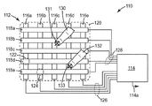
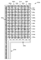
도 1은 본 발명의 일 양태에 따른 터치 감지 디바이스 및 전자기기의 예시적인 실시예를 도시한다. 터치 감지 디바이스(110)는 전자 회로에 연결된 터치 패널(112)을 포함하며, 그것은 간단하게 114로 표시된 하나의 개략적인 상자 내에 그룹화되어, 총칭해서 제어기라고 한다.
터치 패널(112)은 열 전극(column electrode)(116a 내지 116e)과 행 전극(row electrode)(118a 내지 118e)의 5×5 매트릭스를 갖는 것과 같이 도시되지만, 다른 수의 전극 및 다른 매트릭스 크기도 사용될 수 있다. 패널(112)은 통상적으로 사용자가 패널(112)을 통해 물체(컴퓨터, 핸드헬드 디바이스, 휴대폰, 또는 기타 주변 디바이스의 픽셀화된 디스플레이 등)를 볼 수 있도록 실질적으로 투명하다. 경계(120)는 패널(112)의 가시 영역(viewing area)을 나타내고 또한 바람직하게는, 사용되는 경우, 이러한 디스플레이의 가시 영역을 나타낸다. 전극(116a 내지 116e, 118a 내지 118e)은, 평면도에서 볼 때, 가시 영역(120) 상에 공간적으로 분포된다. 설명의 편의상, 전극이 넓고 잘 보이도록 도시되지만, 실제로는 비교적 좁고 사용자에게 잘 안보일 수 있다. 또한, 전극은 가변 폭 - 예를 들어, 전극간 프린지 전계(inter-electrode fringe field)를 증가시킴으써 전극간 용량성 결합(electrode-to-electrode capacitive coupling)에 대한 터치의 효과를 증가시키기 위해 매트릭스의 노드의 근방에서 다이아몬드-형상 또는 기타 형상의 패드의 형태로 증가된 폭 - 을 가지도록 설계될 수 있다. 예시적인 실시예에서, 전극은 인듐 주석 산화물(ITO) 또는 기타 적합한 전기 전도성 물질로 이루어질 수 있다. 깊이 관점에서 볼 때, 열 전극과 행 전극 사이에 상당한 도전성 접촉(contact)이 일어나지 않도록 그리고 주어진 열 전극과 주어진 행 전극 사이의 유일한 유효 전기적 결합(significant electrical coupling)이 용량성 결합이도록 열 전극이 행 전극과 상이한 평면에 있을 수 있다(도 1에서 볼 때, 열 전극(116a 내지 116e)이 행 전극(118a 내지 118e) 아래에 있다). 전극의 매트릭스가 전형적으로 커버 유리, 플라스틱 필름, 기타 아래에 있으며, 따라서 전극이 사용자의 손가락 또는 기타 터치-관련 도구와의 직접적인 물리적 접촉으로부터 보호된다. 이러한 커버 유리, 필름 또는 기타의 노출된 표면은 터치 표면이라고 할 수 있다.
임의의 열 및 행 전극 간의 용량성 결합은 주로 전극들이 서로 가장 가까이 있는 영역에서의 전극들의 기하형태의 함수이다. 이러한 영역은 전극 매트릭스의 "노드"에 해당하며, 이들 중 일부가 도 1에 표시되어 있다. 예를 들어, 열 전극(116a)과 행 전극(118d) 사이의 용량성 결합은 주로 노드(122)에서 일어나고, 열 전극(116b)과 행 전극(118e) 사이의 용량성 결합은 주로 노드(124)에서 일어난다. 도 1의 5×5 매트릭스는 25개의 이러한 노드를 가지며, 이들 중 임의의 노드가, 각자의 열 전극(116a 내지 116e)을 제어기에 개별적으로 결합시키는 제어 라인들(126) 중 하나의 적절한 선택 및 각자의 행 전극(118a 내지 118e)을 제어기에 개별적으로 결합시키는 제어 라인들(128) 중 하나의 적절한 선택을 통해, 제어기(114)에 의해 어드레싱될 수 있다.
사용자의 손가락(130) 또는 기타 터치 구현물이 디바이스(110)의 터치 표면과 접촉 또는 근접 접촉하게 되는 경우, 터치 위치(131)에 도시된 바와 같이, 손가락은 전극 매트릭스와 용량성 결합하여 매트릭스, 특히 터치 위치에 가장 가까이 놓인 전극으로부터 전하를 끌어오게 되고, 이렇게 함으로써 가장 가까운 노드(들)에 해당하는 전극 간의 결합 정전용량은 변하게 된다. 예를 들어, 터치 위치(131)에서의 터치는 전극(116c/118b)에 해당하는 노드에 가장 가깝게 있다. 이하에서 추가로 기술하는 바와 같이, 결합 정전용량의 이러한 변화가 제어기(114)에 의해 검출되고 116c/118b 노드에서 또는 그 근방에서의 터치로서 해석될 수 있다. 바람직하게는, 제어기는, 존재하는 경우, 매트릭스의 모든 노드에서의 정전용량의 변화를 신속하게 검출하도록 구성되고, 노드들 사이에 있는 터치 위치를 보간법에 의해 정확하게 결정하기 위해 이웃 노드에 대한 정전용량 변화의 크기를 분석할 수 있다. 또한, 제어기(114)는 동시에 또는 중복하는 때에 터치 디바이스의 상이한 부분에 가해지는 다수의 개별 터치를 검출하는 데 유리하도록 설계된다. 따라서, 예를 들어, 다른 손가락(132)이, 손가락(130)의 터치와 동시에, 터치 위치(133)에서 디바이스(110)의 터치 표면을 터치하는 경우, 또는 각자의 터치가 적어도 시간적으로 중복하는 경우, 제어기는 바람직하게는 이러한 터치 둘 모두의 위치(131, 133)를 검출하고 터치 출력(114a)에 이러한 위치를 제공할 수 있다. 제어기(114)에 의해 검출될 수 있는 별개의 동시적인 또는 시간적으로 중복하는 터치의 수가 바람직하게는 2로 제한되지 않으며, 예를 들어, 전극 매트릭스의 크기에 따라 3, 4 또는 그 이상일 수 있다.
제어기(114)는 전극 매트릭스의 노드들 중 일부 또는 전부에서의 결합 정전용량을 신속히 결정하는 것을 가능하게 해주는 다양한 회로 모듈 및 구성 성분을 이용할 수 있다. 예를 들어, 제어기는 적어도 하나의 신호 발생기 또는 구동 유닛을 포함할 수 있다. 구동 유닛은 구동 전극으로 지칭되는, 한 세트의 전극에 구동 신호를 전달한다. 도 1의 실시예에서, 열 전극(116a 내지 116e)이 구동 전극으로 사용되거나, 행 전극(118a 내지 118e)이 구동 전극으로 사용될 수 있다. 구동 신호는 다양한 방식으로 전극에 전달될 수 있는데, 예를 들어, 첫번째 구동 전극부터 마지막 구동 전극까지 스캔되는 순서대로 한번에 하나의 구동 전극에 전달된다. 각각의 이러한 전극이 구동될 때, 제어기는 수신 전극이라고 하는 다른 세트의 전극을 모니터링한다. 제어기(114)는 모든 수신 전극에 결합되는 하나 이상의 감지 유닛을 포함할 수 있다. 터치 패널(112)에 대해 이루어진 다수의 컨택을 감지하는 데 적합한 회로는 미국 특허 출원 공개 제2010/0300773호, "고속 다중 터치 디바이스 및 이를 위한 제어기(HIGH SPEED MULTI-TOUCH DEVICE AND CONTROLLER THEREFOR)"에 추가로 기술된다.
제어기는 또한 일련의 응답 신호 입력으로부터 전하를 축적하는 회로를 포함할 수 있다. 이를 위한 예시적인 회로 디바이스는 하나 이상의 축전기(charge accumulator), 예를 들어, 하나 이상의 커패시터를 포함할 수 있고, 구동 신호 및 대응하는 응답 신호의 특성에 따라 그것을 선택한다. 각각의 펄스는 일부 전하 양자(quantum of charge)의 축적을 초래하고, 각각의 추가적인 펄스가 연속하여 더 많이 더해진다. 전하는 또한 한 사이클에서만 결합될 수 있고, 임의의 추가적인 펄스가 단지 노이즈 감소를 위한 전하의 평균화를 가능하게 할 수 있다. 제어기는 또한 축적된 신호의 아날로그 진폭을 디지털 형식으로 변환하기 위한 하나 이상의 아날로그-디지털 변환기(ADC)를 포함할 수 있다. 불필요한 회로 요소의 중복을 피하기 위해 하나 이상의 멀티플렉서가 또한 사용될 수 있다. 물론, 제어기는 또한 바람직하게는 측정된 진폭 및 연관된 파라미터를 저장하는 하나 이상의 메모리 디바이스와, 필요한 계산 및 제어 기능을 수행하는 마이크로프로세서를 포함한다.
임의의 측정 사이클과 연관된 하나 이상의 펄스에 대해 전극 매트릭스 내의 각 노드에 대한 응답 신호와 연관된 축적된 전하의 전압을 측정함으로써, 제어기는 전극 매트릭스의 각 노드에 대한 결합 정전용량에 관련된 측정값들의 매트릭스를 만들 수 있다. 어느 노드(있는 경우)가 터치의 존재로 인한 결합 정전용량의 변화를 경험하는지를 결정하기 위해, 이들 측정된 값이 이전에 획득된 기준 값의 유사한 행렬과 비교될 수 있다.
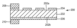
도 2는 본 발명의 일 양태에 따른 다층 구조의 예시적인 실시예를 도시한다. 일 양태에서, 다층 구조(200)는, 예를 들어, 도 1의 터치 감지 디바이스(110)와 같은 터치 감지 디바이스에 사용하기 위한 터치 센서일 수 있다. 다층 구조(200)는 반대 방향의 두 측면을 가지며, 반대 방향의 두 주표면(202a, 202b)을 갖는 중심 중합체 UV 투명 기판(202), 중심 중합체 UV 투명 기판(202)의 제1 주표면(202a) 상의 제1 투명 도전층(204), 및 중심 중합체 UV 투명 기판(202)의 제2 주표면(202b) 상의 제2 투명 도전층(206)을 포함한다. UV 투명성은 본 명세서에서 약 336 nm의 파장에서 시작하여 근적외선까지 연장하여 적어도 약 70%의 투과율을 갖는 것으로 정의된다. 예를 들어, 일부 실시예에서, 중심 중합체 UV 투명 기판(202)은 약 309 nm 미만에서 최대 흡수율, 약 314 nm 미만에서 한계 파장, 및 약 336 nm의 파장에서 적어도 약 70%의 투과율, 및 약 800 nm의 파장에서 약 89%의 투과율을 갖는다. 일부 실시예에서, 투과율은 약 800 nm의 파장에서 약 97%일 수 있다. 적어도 하나의 실시예에서, 중심 중합체 UV 투명 기판(202)의 두께는 약 125 μm이다. 일부 실시예에서, 중심 중합체 UV 투명 기판의 두께의 범위는 약 25 μm 내지 약 175 μm이다. 일부 실시예에서, 중심 중합체 UV 투명 기판(202)은 폴리에스테르, 폴리카보네이트 액정 중합체, 폴리이미드, 및 폴리에틸렌 나프탈레이트로 구성된 그룹에서 선택된다. 적어도 하나의 실시예에서, 중심 중합체 UV 투명 기판(202)은 폴리에틸렌 테레프탈레이트(PET)를 포함한다. 다른 실시예에서, 중심 중합체 UV 투명 기판(202)은, 예를 들어, 약 1.70의 고굴절률을 갖는 폴리에틸렌 나프탈레이트 (PEN), 예를 들어, 약 95%의 고투과율을 갖는 트라이아세테이트 (TAC) 필름, 또는 예를 들어, 약 96%의 고투과율을 갖는 표면처리된 PET를 포함한다. 중심 중합체 UV 투명 기판(202)은 제2 투명 도전층(206)으로부터 제1 투명 도전층(204)을 분리한다. 적어도 하나의 실시예에서, 제1 투명 도전층(204) 및 제2 투명 도전층(206)의 두께는 약 85 nm이다. 일부 실시예에서, 투명 도전층의 두께의 범위는 약 20 nm 내지 약 100 nm이다. 제1 투명 도전층(204) 및 제2 투명 도전층(206)의 두께는 상이하거나, 실질적으로 동일할 수 있다. 일부 실시예에서, 제1 투명 도전층(204) 및 제2 투명 도전층(206)은 인듐 주석 산화물 (ITO)을 포함한다. 일부 실시예에서, ITO는 비결정질이다. 일부 실시예에서, 제1 투명 도전층(204) 및 제2 투명 도전층(206)은 ITO 및 규소 산화물의 층들을 포함하고, 일부 실시예에서, 규소 산화물은 알루미늄으로 도핑되고, 이는 싱가포르 특허 출원 제201105168-7호, "에칭 방법 및 상기 에칭 방법을 이용하여 제조된 디바이스[ETCHING METHOD AND DEVICES PRODUCED USING THE ETCHING METHOD]"에 추가로 기재된 바와 같다. 예를 들어, 적어도 하나의 실시예에서, 투명 도전층은 SiAlO-ITO-SiAlO-ITO 층 구조를 포함하고, 이는 두께가 약 5 nm인 알루미늄으로 도핑된 제1 층의 규소 산화물(SiAlO), 두께가 약 20 nm인 제1 층의 ITO, 두께가 약 40 nm인 알루미늄으로 도핑된 제2 층의 규소 산화물(SiAlO), 및 두께가 약 20 nm인 제2 층의 ITO를 포함한다. 이 실시예에서, 알루미늄으로 도핑된 제1 층의 규소 산화물은 제1 층의 ITO를 중심 중합체 UV 투명 기판에 접착하기 위한 타이층(tie layer)으로 기능한다. 단일층의 ITO에 비교하여, 제2 층의 ITO 상의 알루미늄으로 도핑된 제2 층의 규소 산화물 상의 제1 층의 ITO의 다층 적층물은 개선된 광학 투과율, 감소된 취성(brittleness), 높은 도전성, 및 고온 및 고습 조건에서의 개선된 신뢰성을 제공한다. 제1 투명 도전층(204)은 제1 세트의 전극을 형성하도록 패터닝되고, 제2 투명 도전층(206)은 제2 세트의 전극을 형성하도록 패터닝된다. 적어도 하나의 실시예에서, 전극의 폭은 약 1 mm이다. 일부 실시예에서, 전극은 약 3.5 mm 내지 약 6.5 mm의 범위의 간격 또는 피치로 배치된다. 전극의 폭은 상이하거나, 실질적으로 동일할 수 있다. 일부 실시예에서, 제1 세트의 전극은 제2 세트의 전극에 직교한다. 다른 실시예에서, 제1 세트의 전극 및 제2 세트의 전극은 서로 직교하지 않는다. 일부 실시예에서 투명 도전층 둘 모두 패터닝되거나, 둘 모두 패터닝되지 않지만, 다른 실시예에서 제1 투명 도전층(204) 및 제2 투명 도전층(206) 중에 오직 하나만 패터닝된다. 다층 구조(200)는 제1 투명 도전층(204) 상의 제1 금속성 도전층(208) 및 제2 투명 도전층(206) 상의 제2 금속성 도전층(210)을 추가로 포함한다. 적어도 하나의 실시예에서, 제1 금속성 도전층(208) 및 제2 금속성 도전층(210)의 두께는 약 8 μm이다. 일부 실시예에서, 금속성 도전층의 두께의 범위는 약 3 μm 내지 약 50 μm이고, 예를 들어, 본딩 및 도전성 요구조건에 따라 달라진다. 일 태양에서, 금속성 도전층은 다층 구조의 신호 속도를 유리하게 개선하기 위하여 약 5 μm 내지 약 20 μm 범위의 두께로 제공될 수 있다. 제1 금속성 도전층(208) 및 제2 금속성 도전층(210)의 두께는 상이하거나, 실질적으로 동일할 수 있다. 일부 실시예에서, 제1 금속성 도전층(208) 및 제2 금속성 도전층(210)은 구리, 알루미늄, 금, 은, 니켈, 및 주석으로 구성된 그룹에서 선택된다. 일부 실시예에서, 제1 금속성 도전층(208) 및 제2 금속성 도전층(210)은 복수의 구리 층을 포함한다. 예를 들어, 적어도 하나의 실시예에서, 금속성 도전층은 두께의 범위가 약 100 nm 내지 약 200 nm인 제1 층의 구리, 및 상기 제1층의 구리 상에 배치되는 두께의 범위가 약 6 μm 내지 약 35 μm인 제2 층의 구리를 포함한다. 이 실시예에서, 제1층의 구리는 제2 층의 구리를 상기 투명 도전층에 접착하기 위한 타이층으로서 기능한다. 일부 실시예에서, 제1 금속성 도전층(208)은 제1 세트의 도전성 회로를 형성하도록 패터닝되고, 제2 금속성 도전층(210)은 제2 세트의 도전성 회로를 형성하도록 패터닝된다.
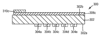
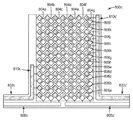
도 3a 및 도 3b는 본 발명의 양태에 따른 다층 구조의 다른 예시적인 실시예를 도시한다. 다층 구조(300)는, 예를 들어, 도 1의 터치 감지 디바이스(110)와 같은 터치 감지 디바이스에 사용하기 위한 터치 센서일 수 있다. 일부 실시예에서, 다층 구조(300)의 두께의 범위는 약 25 μm 내지 약 1 mm이다. 다층 구조(300)의 크기는 의도된 어플리케이션에 기초하여 선택될 수 있다. 일부 실시예에서, 다층 구조(300)는 약 609.6 mm (24 인치) 내지 약 1270 mm (50 인치)의 범위의 대각선 폭 및 3:4의 종횡비를 갖는다. 도 2에 도시된 다층 구조(200)와 유사하게, 다층 구조(300)는 반대 방향의 두 측면을 갖고, 중심 중합체 UV 투명 기판, 중심 중합체 UV 투명 기판의 반대 방향의 두 주표면 각각의 위의 투명 도전층, 및 각각의 투명 도전층 상의 금속성 도전층을 포함한다. 다층 구조(300)에서, 제1 투명 도전층(304)은 제1 세트의 전극(304a 내지 304e)을 형성하도록 패터닝되고, 제2 투명 도전층(306)은 제2 세트의 전극(306a 내지 306f)을 형성하도록 패터닝된다. 전극(304a 내지 304e) 및 전극(306a 내지 306f)은 제1 경계(312) 안쪽에서 제공되고, 다층 구조(300)의 터치 감지 영역을 나타낸다. 일부 실시예에서, 제1 경계(312)는 또한, 사용되는 경우, 디스플레이의 가시 영역을 나타낸다. 도 3a 및 도 3b에 도시된 실시예에서, 5개의 전극(304a 내지 304e) 및 6개의 전극(306a 내지 306f)은 중심 중합체 UV 투명 기판의 반대면 상에 행 전극과 열 전극의 매트릭스를 형성하기 위하여 직교하여 정렬된다. 도 3a 및 도 3b에서 볼 수 있는 바와 같이, 각 전극은 전극간 프린지 필드를 증가시키기 위하여 매트릭스의 노드의 주변에서 직렬로 배열된 다수의 다이아몬드 형상 도전성 패드를 포함함으로써, 전극 간 용량성 결합 상의 터치 효과를 증가시킨다. 일부 실시예에서, 다이아몬드 형상 도전성 패드는 약 3 mm 내지 약 6 mm의 범위의 대각선 폭을 갖는다. 다이아몬드 형상 도전성 패드는 전극(304a 내지 304e)(열 전극)의 도전성 패드와 전극(306a 내지 306f)(행 전극)의 도전성 패드가 기판 주표면의 평면에 수직한 방향으로 중첩되지 않도록 배열된다. 다이아몬드 형상 도전성 패드는 또한 일반적으로 중심 중합체 UV 투명 기판의 한 측면 상에 배치되는 전극의 도전성 패드가 중심 중합체 UV 투명 기판의 반대면 상에 배치되는 4개의 인접한 전극의 도전성 패드의 중심에 배치되도록 배열된다. 다층 구조(300)는 제1 투명 도전층(304) 상의 제1 금속성 도전층(308) 및 제2 투명 도전층(306) 상의 제2 금속성 도전층(310)을 추가로 포함한다. 제1 금속성 도전층(308)은 제1 세트의 도전성 회로(308a 내지 308e)를 형성하도록 패터닝되고, 제2 금속성 도전층(310)은 제2 세트의 도전성 회로(310a 내지 310f)를 형성하도록 패터닝된다. 도전성 회로(308a 내지 308e) 및 도전성 회로(310a 내지 310f)는 제2 경계(314) 안으로 연장되고, 다층 구조(300)의 비-터치 감지 영역을 나타낸다.도전성 회로(308a 내지 308e)는 일반적으로 전극(304a 내지 304e)의 종방향으로 연장되고(열 방향), 도전성 회로(310a 내지 310f)는 일반적으로 전극(306a 내지 306f)의 종방향으로 연장된다(행 방향). 본 발명의 양태에 따른 다층 구조의 장점은 도전성 회로(본 명세서에서 또한 버스 라인으로 지칭됨)는 투명 전극을 터치 감지 디바이스의 전자 회로에 연결하기 위한 미세 피치 상호연결부를 구성하고, 예를 들어, 최소한의 비-터치 감지 영역을 차지하는 터치 감지 영역의 에지를 따라 다층 구조에 포함되고, 이는 다층 구조의 전체 크기를 최소화하고 크기가 큰 개별 커넥터, 고가의 개별 FPC, 투명 전극에 결합하는 ACF, 도전성 잉크 인쇄, 및 가열 공정이 필요없게 한다. 도 3a 및 도 3b에서 볼 수 있는 바와 같이, 도전성 회로(308a 내지 308e) 및 도전성 회로(310a 내지 310f)는 각각 넓은 도전성 패드에 연결되는 좁은 도전성 트레이스를 포함한다. 적어도 하나의 실시예에서, 도전성 트레이스의 폭은 약 250 μm이다. 일부 실시예에서, 도전성 트레이스의 폭의 범위는 30 μm 내지 약 100 μm이다. 도전성 트레이스의 폭은 상이하거나, 실질적으로 동일할 수 있다. 적어도 하나의 실시예에서, 도전성 트레이스는 약 500 μm의 간격 또는 피치로 배치된다. 일부 실시예에서, 도전성 트레이스는 약 60 μm 내지 약 200 μm의 범위의 간격 또는 피치로 배치된다. 일 양태에서, 넓은 도전성 패드는 예를 들어 T 형상의 가요성 인쇄 회로와 같은 개별 가요성 인쇄 회로를 다층 구조(300)의 도전성 패드 및 전자 회로에 결합함으로써 다층 구조(300)를 터치 감지 디바이스의 전자 회로(예를 들어, 제어기 포함)에 연결하는 것을 용이하게 하도록 기능한다. 이 도전성 패드들은 이 연결을 가능하도록 다층 구조의 일측 또는 양측에 제공될 수 있다. 적어도 하나의 실시예에서, 도전성 패드의 폭은 약 250 μm이다. 일부 실시예에서, 도전성 패드의 폭의 범위는 약 75 μm 내지 약 250 μm이다. 일부 실시예에서, 패터닝된 금속성 도전층을 포함하는 비-터치 감지 영역의 넓이는 다층 구조에 사용되는 전극의 수에 비례한다. 행 전극 또는 열 전극의 수는 다층 구조의 응용 및 크기에 따라 달라질 수 있다. 일부 실시예에서, 다층 구조(300)의 일측 상의 패터닝된 제1 금속성 도전층(308)의 도전성 트레이스는 상기 트레이스가 기판 주표면의 평면에 수직한 방향으로 중첩되지 않도록 다층 구조(300)의 다른 일측 상의 패터닝된 제2 금속성 도전층(310)의 도전성 트레이스로부터 상쇄된다. 유익하게도, 그와 같은 배열에서, 트레이스는 용량성 결합을 하지 않음으로써, 전기적 간섭을 피한다.
도 4는 본 발명의 일 양태에 따른 다층 구조의 다른 예시적인 실시예를 도시한다. 다층 구조(400)는, 예를 들어, 도 1의 터치 감지 디바이스(110)와 같은 터치 감지 디바이스에 사용하기 위한 터치 센서일 수 있다. 도 2에 도시된 다층 구조(200)와 유사하게, 다층 구조(400)는 반대 방향의 두 측면을 갖고, 반대 방향의 두 주표면(402a, 402b)을 갖는 중심 중합체 UV 투명 기판(402), 중심 중합체 UV 투명 기판(402)의 제1 주표면(402a) 상의 제1 투명 도전층(404), 중심 중합체 UV 투명 기판(402)의 제2 주표면(402b) 상의 제2 투명 도전층(406), 제1 투명 도전층(404) 상의 제1 금속성 도전층(408), 및 제2 투명 도전층(406) 상의 제2 금속성 도전층(410)을 포함한다. 제1 투명 도전층(404)은 제1 세트의 전극을 형성하기 위하여 패터닝되고, 제2 투명 도전층(406)은 제2 세트의 전극을 형성하기 위하여 패터닝된다. 일부 실시예에서, 제1 금속성 도전층(408)은 제1 세트의 도전성 회로를 형성하도록 패터닝되고, 제2 금속성 도전층(410)은 제2 세트의 도전성 회로를 형성하도록 패터닝된다. 다층 구조(400)는 제1 투명 도전층(404) 상에 배치되는 제1 접착제층(416) 및 제2 투명 도전층(406) 상에 배치되는 제2 접착제층(418)을 추가로 포함한다. 제1 투명 도전층(404)은 제1 세트의 전극을 형성하기 위하여 패터닝되고, 제2 투명 도전층(406)은 제2 세트의 전극을 형성하기 위하여 패터닝되는 일부 실시예에서, 제1 접착제층(416)은 그것이 제1 세트의 전극 및 제1 세트의 전극에 의해 커버되지 않는 중심 중합체 UV 투명 기판(402)의 일부를 실질적으로 커버하도록 배치되고, 제2 접착제층(418)은 그것이 제2 세트의 전극 및 제2 세트의 전극에 의해 커버되지 않는 중심 중합체 UV 투명 기판(402)의 일부를 실질적으로 커버하도록 배치된다. 제1 금속성 도전층(408)은 제1 세트의 도전성 회로를 형성하기 위하여 패터닝되고, 제2 금속성 도전층(410)은 제2 세트의 도전성 회로를 형성하기 위하여 패터닝되는 일부 실시예에서, 도전성 회로의 적어도 일부는 접착제층에 의해 커버되지 않는다. 일 양태에서, 이것은 개별 가요성 인쇄 회로를 다층 구조(400)의 도전성 패드 및 전자 회로에 결합함으로써 터치 감지 디바이스의 전자 회로(예를 들어, 제어기 포함)에 다층 구조(400)를 연결하는 것을 가능하게 한다. 적어도 하나의 실시예에서, 제1 접착제층(416) 및 제2 접착제층(418)의 두께는 약 50 μm이다. 일부 실시예에서, 접착제층의 두께의 범위는 약 50 μm 내지 약 100 μm이다. 제1 접착제층(416) 및 제2 접착제층(418)의 두께는 상이하거나, 실질적으로 동일할 수 있다. 일부 실시예에서, 제1 접착제층(416) 및 제2 접착제층(418)은 감압 접착제를 포함한다. 일부 실시예에서, 제1 접착제층(416) 및 제2 접착제층(418)은 광학적 투명 접착제를 포함한다. 광학적 투명 접착제는 대전방지 특성을 가질 수 있다. 다층 구조(400)는 제1 접착제층에 부착되는 제1 하드 코드층(420) 및 제2 접착제층(418)에 부착되는 제2 하드 코트층(422)을 추가로 포함할 수 있다. 적어도 하나의 실시예에서, 제1 하드 코트층(hard coat layer)(420) 및 제2 하드 코트층(422)의 두께는 약 6 μm이다. 일부 실시예에서, 하드 코트층들의 두께의 범위는 약 3 μm 내지 약 6 μm이다. 제1 하드 코트층(420) 및 제2 하드 코트층(422)의 두께는 상이하거나, 실질적으로 동일할 수 있다. 적어도 하나의 실시예에서, 제1 하드 코트층(420) 및 제2 하드 코트층(422)은 PET를 포함한다. 일부 실시예에서, 하드 코트층은, 예를 들어, PET, PEN, 또는 트라이아세테이트(TAC) 필름을 포함하는 투명 기판에 도포되는 하드 코트를 포함할 수 있다. 하드 코트는 예를 들어, 스크래치로부터 기판을 보호하기 위하여, 예를 들어, 실리카 및 알루미나와 같은 나노입자를 포함할 수 있다. 하드 코트는 또한 반사방지 및 지문방지 특성을 가질 수 있다.
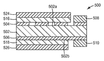
도 5는 본 발명의 일 양태에 따른 다층 구조의 다른 예시적인 실시예를 도시한다. 다층 구조(500)는, 예를 들어, 도 1의 터치 감지 디바이스(110)와 같은 터치 감지 디바이스에 사용하기 위한 터치 센서일 수 있다. 도 4에 도시된 다층 구조(400)와 유사하게, 다층 구조(500)는 반대 방향의 두 측면을 갖고, 반대 방향의 두 주표면(502a, 502b)을 갖는 중심 중합체 UV 투명 기판(502), 중심 중합체 UV 투명 기판(502)의 제1 주표면(502a)상의 제1 투명 도전층(504), 중심 중합체 UV 투명 기판(502)의 제2 주표면(502b) 상의 제2 투명 도전층(506), 제1 투명 도전층(504) 상의 제1 금속성 도전층(508), 제2 투명 도전층(506) 상의 제2 금속성 도전층(510), 제1 투명 도전층(504) 상에 배치되는 제1 접착제층(516), 제2 투명 도전층(506) 상에 배치되는 제2 접착제층(518)을 포함한다. 제1 투명 도전층(504)은 제1 세트의 전극을 형성하도록 패터닝되고, 제2 투명 도전층(506)은 제2 세트의 전극을 형성하도록 패터닝된다. 일부 실시예에서, 제1 금속성 도전층(508)은 제1 세트의 도전성 회로를 형성하도록 패터닝되고, 제2 금속성 도전층(510)은 제2 세트의 도전성 회로를 형성하도록 패터닝된다. 제1 투명 도전층(504)은 제1 세트의 전극을 형성하기 위하여 패터닝되고, 제2 투명 도전층(506)은 제2 세트의 전극을 형성하기 위하여 패터닝되는 일부 실시예에서, 제1 접착제층(516)은 그것이 제1 세트의 전극 및 제1 세트의 전극에 의해 커버되지 않는 중심 중합체 UV 투명 기판(502)의 일부를 실질적으로 커버하도록 배치되고, 제2 접착제층(518)은 그것이 제2 세트의 전극 및 제2 세트의 전극에 의해 커버되지 않는 중심 중합체 UV 투명 기판(502)의 일부를 실질적으로 커버하도록 배치된다. 제1 금속성 도전층(508)은 제1 세트의 도전성 회로를 형성하기 위하여 패터닝되고, 제2 금속성 도전층(510)은 제2 세트의 도전성 회로를 형성하기 위하여 패터닝되는 일부 실시예에서, 도전성 회로의 적어도 일부는 접착제층에 의해 커버되지 않는다. 일 양태에서, 이것은 개별 가요성 인쇄 회로를 다층 구조(500)의 도전성 패드 및 전자 회로에 결합함으로써 터치 감지 디바이스의 전자 회로(예를 들어, 제어기 포함)에 다층 구조(500)를 연결하는 것을 가능하게 한다. 다층 구조(500)는 제1 접착제층(516)에 부착되는 유리 패널(524) 및 제2 접착제층(518)에 부착되는 디스플레이 유닛(526)을 추가로 포함한다. 적어도 하나의 실시예에서, 유리 패널(524)의 두께는 약 0.7 mm이다. 일부 실시예에서, 유리 패널(524)의 두께의 범위는 약 0.5 mm 내지 약 1 mm이다. 일 태양에서, 유리 패널(524)은 마모와 손상으로부터 다층 구조를 보호하는 기능을 한다. 적어도 하나의 실시예에서, 디스플레이 유닛(526)은 액정 디스플레이 (LCD) 패널이다.
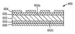
도 6은 본 발명의 일 양태에 따른 다층 구조의 다른 예시적인 실시예를 도시한다. 다층 구조(600)는, 예를 들어, 도 1의 터치 감지 디바이스(110)와 같은 터치 감지 디바이스에 사용하기 위한 터치 센서일 수 있다. 다층 구조(600)는 반대 방향의 두 측면을 가지며, 반대 방향의 두 주표면(602a, 602b)을 갖는 중심 중합체 UV 투명 기판(602), 중심 중합체 UV 투명 기판(602)의 제1 주표면(602a) 상의 제1 코팅(628), 중심 중합체 UV 투명 기판(602)의 제2 주표면(602b) 상의 제2 코팅(630), 제1 코팅(628) 상의 제1 투명 도전층(604), 및 제2 코팅(630) 상의 제2 투명 도전층(606)을 포함한다. 적어도 하나의 실시예에서, 중심 중합체 UV 투명 기판(602)의 두께는 약 125 μm이다. 일부 실시예에서, 중심 중합체 UV 투명 기판의 두께의 범위는 약 25 μm 내지 약 200 μm이다. 일부 실시예에서, 중심 중합체 UV 투명 기판(602)은 폴리에스테르, 폴리카보네이트, 액정 중합체, 폴리이미드, 및 폴리에틸렌 나프탈레이트로 구성된 그룹에서 선택된다. 적어도 하나의 실시예에서, 중심 중합체 UV 투명 기판(602)은 PET를 포함한다. 일부 실시예에서, 제1 코팅(628) 및 제2 코팅(630)은 중심 중합체 UV 투명 기판(602)의 올리고머 이동을 방지함으로써 탁해짐의 정도를 줄이는 기능을 한다. 적어도 하나의 실시예에서, 제1 코팅(628) 및 제2 코팅(630)의 두께는 약 1 μm이다. 일부 실시예에서, 코팅의 두께의 범위는 1 μm 내지 약 6 μm이다. 제1 코팅(628) 및 제2 코팅(630)의 두께는 상이하거나, 실질적으로 동일할 수 있다. 유익하게도, 투명 도전층들 사이의 정전용량은 코팅 두께를 증가(또는 감소)시킴으로써 증가(또는 감소)될 수 있다. 적어도 하나의 실시예에서, 제1 코팅(628) 및 제2 코팅(630)의 굴절률은 약 1.50이다. 일부 실시예에서, 코팅의 굴절률의 범위는 약 1.47 내지 약 2.00이다. 일부 실시예에서, 다층 구조의 일측 상의 굴절률은 타측 상의 굴절률과 상이하다. 일부 실시예는 상이한 굴절률을 갖는 다중 코팅을 포함한다. 적어도 하나의 실시예에서, 코팅은 예를 들어, 아크릴레이트 또는 에폭시와 같은 적합한 UV 경화성 접착제를 포함한다. 적합한 UV 경화성 접착제에는 추가적인 나노입자가 제공되거나 제공되지 않을 수 있다. 예를 들어, 약 1 nm 내지 약 75 nm 범위의 크기를 갖는 실리카 또는 지르코니아와 같은 나노입자는 코팅 제제에 분산될 수 있다. 적어도 하나의 실시예에서, 나노입자의 크기는 코팅 층의 두께를 초과하지 않는다. 중심 중합체 UV 투명 기판(602), 제1 코팅(628), 및 제2 코팅(630)은 제2 투명 도전층(606)으로부터 제1 투명 도전층(604)을 분리한다. 적어도 하나의 실시예에서, 제1 투명 도전층(604) 및 제2 투명 도전층(606)의 두께는 약 20 nm이다. 일부 실시예에서, 투명 도전층의 두께의 범위는 약 15 nm 내지 약 30 nm이다. 제1 투명 도전층(604) 및 제2 투명 도전층(606)의 두께는 상이하거나, 실질적으로 동일할 수 있다. 일부 실시예에서, 제1 투명 도전층(604) 및 제2 투명 도전층(606)은 인듐 주석 산화물 (ITO)을 포함한다. 일부 실시예에서, ITO는 비결정질이다. 일부 실시예에서, 제1 투명 도전층(604) 및 제2 투명 도전층(606)은 ITO 및 규소 산화물 층들을 포함한다. 일부 실시예에서, 규소 산화물은 알루미늄으로 도핑된다. 제1 투명 도전층(604)은 제1 세트의 전극을 형성하도록 패터닝되고, 제2 투명 도전층(606)은 제2 세트의 전극을 형성하도록 패터닝된다. 적어도 하나의 실시예에서, 전극의 폭은 약 1 mm이다. 일부 실시예에서, 전극은 약 3.5 mm 내지 약 6.5 mm의 범위의 간격 또는 피치로 배치된다. 전극의 폭은 상이하거나, 실질적으로 동일할 수 있다. 일부 실시예에서, 제1 세트의 전극은 제2 세트의 전극에 직교한다. 다른 실시예에서, 제1 세트의 전극 및 제2 세트의 전극은 서로 직교하지 않는다.
도 7a 내지 도 7b는 본 발명의 양태에 따른 다층 구조의 다른 예시적인 실시예를 도시한다. 다층 구조(700)는, 예를 들어, 도 1의 터치 감지 디바이스(110)와 같은 터치 감지 디바이스에 사용하기 위한 터치 센서일 수 있다. 도 2에 도시된 다층 구조(200)와 유사하게, 다층 구조(700)는 반대 방향의 두 측면을 갖고, 중심 중합체 UV 투명 기판, 중심 중합체 UV 투명 기판의 반대 방향의 두 주표면의 각각 위의 투명 도전층, 및 각각의 투명 도전층 상의 금속성 도전층을 포함한다. 다층 구조(700)는 도 3a 내지 도 3b에 도시된 다층 구조(300)와 유사하다. 다층 구조(700)는 전극(304a 내지 304e)의 종방향으로 (열 방향) 비-터치 감지 영역으로부터 연장되는 제1 종방향 커넥터 테일(connector tail)(732) 및 전극(306a 내지 306f)의 종방향으로 (행 방향) 비-터치 감지 영역으로부터 연장되는 제2 종방향 커넥터 테일(734)을 포함한다는 점에서 다층 구조(700)는 도 3a 내지 도 3b에 도시된 다층 구조(300)와 다르다. 도전성 회로(308a 내지 308e) 및 도전성 회로(310a 내지 310f)는 다층 구조(700)의 비-터치 감지 영역으로, 각각 커넥터 테일(732) 및 커넥터 테일(734)을 따라 연장된다. 일 양태에서, 커넥터 테일은 하나 이상의 개별적인 가요성 인쇄 회로가 필요 없이, 도전성 패드를 전자 회로에 직접 결합함으로써 다층 구조(700)의 넒은 도전성 패드와 터치 감지 디바이스의 전자 회로 (예를 들어, 제어기를 포함) 사이에 직접 연결을 가능하도록 기능한다. 따라서, 하나 이상의 개별적인 가요성 인쇄 회로를 포함하는 멀티-피스 구조 대신에, 단일-피스 구조가 제공될 수 있다. 하나 이상의 개별적인 가요성 인쇄 회로가 필요없게 만드는 것은 또한 하나 이상의 가요성 인쇄 회로를 다층 구조에 결합하는 것, 예를 들어, 특히 다층 구조가 유리 패널에 라미네이트되는 것, 과 관련된 어려움을 해소해준다. 커넥터 테일은 중심 중합체 UV 투명 기판을 원하는 형상으로 다이 커팅(die-cutting)함으로써 형성될 수 있다. 일 양태에서, 커넥터 테일의 길이는 전자 회로의 위치 및 전자 회로-비 터치 감지 영역 간의 거리에 기초하여 선택될 수 있다.
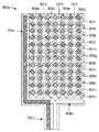
의도된 어플리케이션에 적합한 바와 같이, 하나 이상의 커넥터 테일은 임의의 적합한 위치에서 다층 구조의 비 터치 감지 영역으로부터 연장될 수 있다. 도 8a 내지 도 8e는 본 발명의 여러 양태에 따른 다층 구조의 예시적인 실시예를 도시하고, 다양한 예시 커넥터 테일 구성들이 도시된다. 도 8a를 참조하면, 다층 구조(800a)는 전극(804a 내지 804g)의 종방향으로 (열 방향) 비 터치 감지 영역으로부터 연장되는 종방향 커넥터 테일(832a)을 포함한다. 전극(804a 내지 804g)과 관련된 도전성 회로(808a) 및 전극(806a 내지 806l)과 관련된 도전성 회로(810a)는 커넥터 테일(832a)을 따라 길게 다층 구조(800a)의 비 터치 감지 영역으로 연장된다. 도 8b를 참조하면, 다층 구조(800b)는 전극(806a 내지 806l)의 종방향으로 (행 방향) 비 터치 감지 영역으로부터 연장되는 종방향 커넥터 테일(832b)을 포함한다. 전극(804a 내지 804g)과 관련된 도전성 회로(808b) 및 전극(806a 내지 806l)과 관련된 도전성 회로(810b)는 커넥터 테일(832b)을 따라 길게 다층 구조(800b)의 비 터치 감지 영역으로 연장된다. 도 8c를 참조하면, 다층 구조(800c)는 전극(806a 내지 806l)의 종방향으로 (행 방향) 비 터치 감지 영역으로부터 연장되는 제1 종방향 커넥터 테일(832c)을 포함한다. 전극(804a 내지 804c)과 관련된 도전성 회로(808c) 및 전극(806a 내지 806e)과 관련된 도전성 회로(810c)는 커넥터 테일(832c)을 따라 길게 다층 구조(800c)의 비 터치 감지 영역으로 연장된다. 다층 구조(800c)는 제1 커넥터 테일(832c)의 반대 쪽에서 전극(806a 내지 806l)의 종방향으로 (행 방향) 비 터치 감지 영역으로 연장되는 제2 종방향 커넥터 테일(832c')을 포함한다. 전극(804d 내지 804g)과 관련된 도전성 회로(808c') 및 전극( 806f 내지 806l)과 관련된 도전성 회로(810c')는 커넥터 테일(832c')을 따라 길게 다층 구조(800c)의 비 터치 감지 영역으로 연장된다. 도 8d를 참조하면, 다층 구조(800d)는 전극(806a 내지 806l)의 832d 종방향으로 (행 방향) 비 터치 감지 영역으로부터 연장되는 종방향 커넥터 테일(832d)을 포함한다. 전극(804a 내지 804g)과 관련된 도전성 회로(808d) 및 전극(806a 내지 806l)과 관련된 도전성 회로(810d)는 커넥터 테일(832d)을 따라 길게 다층 구조(800d)의 비 터치 감지 영역으로 연장된다. 도 8e를 참조하면, 다층 구조(800e)는 전극(804a 내지 804g)의 종방향으로 (열 방향) 비 터치 감지 영역으로부터 연장되는 종방향 커넥터 테일(832e)을 포함한다. 전극(804a 내지 804g)과 관련된 도전성 회로(808e) 및 전극(806a 내지 806l)과 관련된 도전성 회로(810e)는 커넥터 테일(832e)을 따라 길게 다층 구조(800e)의 비 터치 감지 영역으로 연장된다.
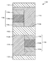
일부 실시예에서, 비 터치 감지 영역의 도전성 회로 및/또는 다층 구조의 커넥터 테일은 보호층에 의해 보호된다. 보호층을 제공하는 것은 예를 들어, 도전성 회로의 부식 및 물리적 손상을 방지할 수 있다. 도 9는 그와 같은 보호층을 포함하는 본 발명의 양태에 따른 다층 구조의 예시적인 실시예를 도시한다. 다층 구조(900)는, 예를 들어, 도 1의 터치 감지 디바이스(110)와 같은 터치 감지 디바이스에 사용하기 위한 터치 센서일 수 있다. 도 4에 도시된 다층 구조(400)와 유사하게, 다층 구조(900)는 반대 방향의 두 측면을 갖고, 반대 방향의 두 주표면(902a, 902b)을 갖는 중심 중합체 UV 투명 기판(902), 중심 중합체 UV 투명 기판(902)의 제1 주표면(902a)상의 제1 투명 도전층(904), 중심 중합체 UV 투명 기판(902)의 제2 주표면(902b) 상의 제2 투명 도전층(906), 제1 투명 도전층(904) 상의 제1 금속성 도전층(908), 제2 투명 도전층(906) 상의 제2 금속성 도전층(910), 제1 투명 도전층(904) 상에 배치되는 제1 접착제층(916), 제2 투명 도전층(906) 상에 배치되는 제2 접착제층(918), 제 1 접착제층(916)에 부착되는 제1 하드 코트층(920), 제2 접착제층(918)에 부착되는 제2 하드 코트층(922)을 포함한다. 다층 구조(900)는 제1 금속성 도전층(908) 상에 제1 보호층(936) 및 제 2 금속성 도전층(910) 상에 제2 보호층(938)을 추가로 포함한다. 도 9에 도시된 실시예에서, 보호층은 비 터치 감지 영역(도 9에서 "A"로 표시됨) 및 커넥터 테일 영역(도 9에서 "B"로 표시됨) 둘 모두의 금속성 도전층 상에 배치되어 예를 들어 이들 영역의 도전성 회로의 보호를 제공한다. 일부 실시예에서, 보호층은 비 터치 감지 영역과 커넥터 테일 영역 중 오직 한 곳의 금속성 도전층 상에 배치된다. 일부 실시예에서, 금속성 도전층의 단지 일부분만이 보호층으로 커버된다. 예를 들어, 제1 금속성 도전층(908)은 제1 세트의 도전성 회로를 형성하기 위하여 패터닝되고, 제2 금속성 도전층(910)은 제2 세트의 도전성 회로를 형성하기 위하여 패터닝되고, 제1 보호층(936) 및 제2 보호층(938)은 도전성 회로를 커버하는 것에 대응하여 패터닝될 수 있다. 일 양태에서, 다층 층 구조가 각 금속성 도전층 상에 패터닝된 포토이미지 마스크(photoimaging mask)를 포함하도록, 보호층이 포토이미지 마스크일 수 있다. 적어도 하나의 실시예에서, 제1 보호층(936) 및 제2 보호층(938)의 두께는 약 25 μm이다. 일부 실시예에서, 보호층의 두께의 범위는 약 12 μm 내지 약 25 μm이다. 제1 보호층(936) 및 제2 보호층(938)의 두께는 상이하거나, 실질적으로 동일할 수 있다. 보호층은 다층 구조의 커넥터 테일 영역의 두께가 다층 구조의 비 터치 감지 영역의 두께와 다를 수 있고, 이는 의도된 응용에 적합한 바와 같다. 보호층은 예를 들어 은, 니켈, 금, 및 주석과 같은 금속을 포함할 수 있다. 금속성 보호층의 두께의 범위는 약 0.03 μm 내지 약 1 μm일 수 있다.
본 발명의 여러 양태에 따른 다층 구조를 만드는 것은 다양한 방법으로 수행될 수 있다. 그것은 포토이미지 층을 도포하고 패터닝하는 단계 및 하부층을 에칭하는 단계를 포함한다. 본 발명의 여러 양태에 따른 다층 구조를 만드는 방법의 이득은 우수한 층간 정착으로 인한 높은 생산 수율, 예를 들어, 예시적인 종래 구조의 5 층에서 본 발명의 양태에 따른 예시적인 구조의 3 층으로 감소된 층 수, 감소된 공정 단계 수, 및 생산 비용의 감소를 포함한다. 또한, 본 발명의 여러 양태에 따른 다층 구조를 만드는 방법은 투명 도전층 사이에 공기 거품 및 외부 물질을 방지하고, 예를 들어 유전성 매체로서 PET를 사용하여 투명 도전층 사이의 미끄러짐을 방지하고, 더 얇은 다층 구조를 만들고, 패터닝된 투명 도전층이 나안으로 식별할 수 없는 구조를 제공할 수 있다. 도 10a 내지 도 10i는 본 발명의 일 양태에 따른 다층 구조를 만드는 예시적인 방법의 단계를 도시한다.
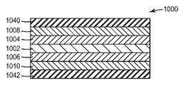
도 10a를 참조하면, 다층 구조(1000)가 제공된다. 다층 구조(1000)는 반대 방향의 두 측면을 갖고, 반대 방향의 두 주표면(1002a, 1002b)을 갖는 중심 중합체 UV 투명 기판(1002), 중심 중합체 UV 투명 기판(1002)의 제1 주표면(1002a) 상의 제1 투명 도전층(1004), 중심 중합체 UV 투명 기판(1002)의 제2 주표면(1002b) 상의 제2 투명 도전층(1006), 제1 투명 도전층(1004) 상의 제1 금속성 도전층(1008), 및 제2 투명 도전층(1006) 상의 제2 금속성 도전층(1010)을 포함한다. 다층 구조(1000)는 다양한 방법으로 제조될 수 있다. 예를 들어, 투명 도전층은 중심 중합체 UV 투명 기판의 롤 상으로 스퍼터링될 수 있고, 금속성 도전층은 투명 도전층 상으로 스퍼터링될 수 있다. 투명 도전층들은 중심 중합체 UV 투명 기판 상에 동시에 또는 순차적으로 배치될 수 있다. 일부 실시예에서, 제1 투명 도전층(1004) 및 제2 투명 도전층(1006)을 동시에 도포하는 것이 더 효율적이고 더 우수한 층 정렬을 제공할 수 있다. 금속성 도전층은 투명 도전층 상에 동시에 또는 순차적으로 배치될 수 있다. 일부 실시예에서, 제1 금속성 도전층(1008) 및 제2 금속성 도전층(1010)을 동시에 도포하는 것이 더 효율적이고 더 우수한 층 정렬을 제공할 수 있다. 일 양태에서, 금속성 도전층(예를 들어, 구리)의 경도는 투명 도전층(예를 들어, ITO)의 경도보다 클 수 있다. 동시에 하는 방법에서, 이것은 제조 공정 중 스크래치로부터 투명 도전층을 보호하는 것을 돕는데, 그렇지 않으면 투명 도전층의 파손되기 쉬운 특성으로 인해 수율 손실을 일으킬 수도 있다. 또한, 금속성 도전층은 양면에 동시 UV 노출을 돕는데, 그렇지 않으면 중심 중합체 UV 투명 기판(예를 들어, PET) 및 투명 도전층의 UV 투과성으로 인해 불가능할 수도 있다.
도 10b 내지 도 10c를 참조하면, 투명 도전층을 위한 원하는 패턴을 갖는 포토이미지 마스크를 형성하기 위하여 두 금속성 도전층 상에 제1 포토이미지 층(1040, 1042)이 도포되고(도 10b) 패터닝된다(도 10c). 다른 방법에서, 포토이미지 마스크는 투명 도전층 및 금속성 도전층을 위한 원하는 패턴을 갖는다. 제1 포토이미지 층(1040, 1042)은 표준 라미네이팅 기법을 사용하여 도포될 수 있다. 제1 포토이미지 층(1040, 1042)을 도포하는 것은 동시에 또는 순차적으로 될 수 있다. 일부 실시예에서, 제1 포토이미지 층(1040, 1042)을 동시에 도포하는 것은 더 효율적이고 더 우수한 층 정렬을 제공할 수 있다. 적어도 하나의 실시예에서, 제1 포토이미지 층의 두께의 범위는 약 35 μm 내지 약 50 μm이다. 제1 포토이미지 층(1040, 1042)은 마스크를 통해 UV 광에 노출됨으로써, 포토이미지 층의 노출된 부분을 가교결합하고, 가교결합되지 않은 부분이 용해되어 원하는 패턴이 드러날 때까지, 예를 들어, 0.5 중량% 내지 1.5 중량% 카보네이트 용액의 희석된 수용액으로 포토이미지 층을 현상함으로써 패터닝될 수 있다. 제1 포토이미지 층(1040, 1042)을 패터닝하는 것은 동시에 또는 순차적으로 될 수 있다. 일부 실시예에서, 제1 포토이미지 층(1040, 1042)을 동시에 패터닝하는 것은 더 효율적이고 더 우수한 패턴 정렬을 제공할 수 있다. 동시 패터닝의 부분으로서, 다층 구조(1000)의 반대 측면 상의 포토이미지 층은 동시에 UV 광에 노출될 수 있다. 본 발명의 여러 양태에서 사용될 수 있는 제1 포토이미지 층(1040, 1042)의 예는 네가티브 수용성 처리 중합성 광경화성 조합물을 포함하고, 이는 또한 포토레지스트로 지칭되고, 미국 특허 제3,469,982호, 제3,448,098호, 제3,867,153호, 및 제3,526,504호에 포함된 것과 같다. 상기 포토레지스트는 적어도 하나의 중합체, 추가 가교결합 단량체 유닛 및 광개시제를 포함한다. 포토레지스트에서 사용되는 중합체의 예는 메틸메타크릴레이트, 에틸 아크릴레이트 및 아크릴산의 공중합체 및 스티렌 및 말레산 무수물 아이소부틸 에스테르의 공중합체 등을 포함한다. 가교결합성 단량체 유닛은 트라이메틸올 프로판 트라이아크릴레이트와 같은 멀티아크릴레이트일 수 있다. 본 발명의 여러 양태에서 사용될 수 있는 일부 수용성 처리 네가티브 포토레지스트의 예는 폴리메틸-메타크릴레이트로부터 나온다.
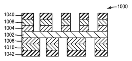
도 10d를 참조하면, 포토이미지 마스크에 의해 노출된 제1 금속성 도전층(1008), 제2 금속성 도전층(1010), 제1 투명 도전층(1004), 및 제2 투명 도전층(1006)의 일부분들이 에칭되고, 이로써 제1 투명 도전층(1004)은 제1 세트의 전극을 형성하도록 패터닝되고, 제2 투명 도전층(1006)은 제2 세트의 전극을 형성하도록 패터닝된다. 유용한 에칭액은 염화 제2구리 및 염화 제2철 및 염산, 인산 및 질산과 같은 무기산을 포함하는 수용성 산화 환원 금속 염화물으로, 이는 싱가포르 특허 출원 제201105168-7호, "에칭 방법 및 상기 에칭 방법을 사용하여 제조된 디바이스[ETCHING METHOD AND DEVICES PRODUCED USING THE ETCHING METHOD]"에 추가로 기재된 바와 같다. 유용한 에칭액의 농도는 에칭될 투명 도전층 및 금속성 도전층의 두께뿐만 아니라 선택된 포토레지스트의 유형 및 두께에 따라 달라진다. 유용한 염화 제2구리 농도의 범위는 약 100 g/L 내지 약 180 g/L이고, 염산의 농도는 약 0.04 N 내지 약 2 N이다. 에칭 단계는 투명 도전층 및 금속성 도전층의 마스크되지 않은 영역을 산화 환원 금속 염화물 에칭액에 접촉시킴으로써 수행된다. 에칭 시간은 에칭될 투명 도전층 및 금속성 도전층의 유형 및 두께에 따라 달라지고 통상적으로 약 10 초 내지 약 20 분이다. 예를 들어, 염화 제2구리 에칭액이 사용되는 경우, 두께가 약 95 nm (약 20 nm ITO + 약 45 nm SiAlO + 약 20 nm ITO)인 ITO-SiAlO-ITO 투명 도전층 및 두께가 약 8 μm인 구리 금속성 도전층을 위한 에칭 시간은 약 2 분이다. 에칭 용액은 일반적으로 약 50℃ 내지 약 80℃의 온도에 있다. 다층 구조(1000)의 반대 측면 상의 투명 도전층들을 에칭하는 것은 동시에 또는 순차적으로 될 수 있다. 일부 실시예에서, 다층 구조(1000)의 반대 측면 상의 투명 도전층을 동시에 에칭하는 것이 더 효율적일 수 있다. 다층 구조 (1000)의 반대 측면 상의 금속성 도전층들을 에칭하는 것은 동시에 또는 순차적으로 될 수 있다. 일부 실시예에서, 다층 구조(1000)의 반대 측면 상의 금속 도전층들을 동시에 에칭하는 것이 더 효율적일 수 있다. 일 양태에서, 염화 제2구리 에칭액은 투명 도전층(예를 들어, ITO)과 금속성 도전층(예를 들어, 구리)을 동시 에칭할 수 있게 함으로써, 투명 도전층 및 금속성 도전층을 순차적으로 에칭하기 위한 별개의 두 에칭액을 필요없게 만들 수 있다.
도 10e를 참조하면, 포토이미지 마스크는 제거된다. 이것은 다층 구조(1000)를 약 40℃ 내지 약 50℃ 의 온도에서 30 % 내지 50 % 모노에탄올아민 용액 안에 배치함으로써 수행될 수 있다.
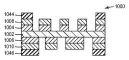
도 10f 내지 도 10g를 참조하면, 금속성 도전층을 위한 원하는 패턴을 갖는 포토이미지 마스크를 형성하기 위하여 각 금속성 도전층의 남은 부분 위에 제2 포토이미지 층(1044, 1046)이 도포되고(도 10f) 패터닝된다(도 10g). 다른 방법으로, 예를 들어, 포토이미지 마스크가 투명 도전층 및 금속성 도전층을 위한 원하는 패턴을 갖는 경우, 포토이미지 마스크는 금속성 도전층의 원하는 패턴을 보호한다. 일부 실시예에서, 제1 금속성 도전층(1008)은 제1 세트의 도전성 회로를 형성하도록 패터닝되고, 제2 금속성 도전층(1010)은 제2 세트의 도전성 회로를 형성하도록 패터닝된다. 적어도 하나의 실시예에서, 금속성 도전층들 중 하나 또는 둘 모두를 위한 원하는 패턴은 투명 도전층을 예를 들어 터치 감지 디바이스와 같은 디바이스에 연결하기 위한 회로를 포함한다. 제2 포토이미지 층(1044, 1046)을 도포하고 패터닝하는 것은 도 10b 내지 도 10c에 대하여 상기 기재된 바와 같이 수행될 수 있다.
도 10h를 참조하면, 제1 금속성 도전층(1008) 및 제2 금속성 도전층(1010)의 노출된 부분이 에칭된다. 금속성 도전층의 노출된 부분의 에칭은 도 10d에 대하여 상기 기재한 바와 같이 수행될 수 있다. 적어도 하나의 실시예에서, 금속성 도전층들 중에서 노출된 부분은 ITO를 에칭하지 않는 에칭액으로 에칭된다. 예를 들어, 에칭액은 암모니아 계열일 수 있다. 암모니아 계열 에칭액은 투명 도전층(예를 들어, ITO-SiAlO-ITO)에 영향을 주지 않고 금속성 도전층(예를 들어, 구리)을 선택적으로 에칭할 수 있다.
도 10i를 참조하면, 포토이미지 마스크가 제거된다. 이것은 다층 구조(1000)를 약 40℃ 내지 약 50℃ 의 온도에서 30 % 내지 50 % 모노에탄올아민 용액 안에 배치함으로써 수행될 수 있다.
도11은 패터닝된 투명 도전층이 적어도 중심 중합체 UV 투명 기판과 굴절률 정합되는 예시적인 실시예를 도시한다. 결과적으로, 패터닝된 투명 도전층의 패턴은 나안으로 식별할 수 없다. 일 양태에서, 다층 구조(1100)는, 예를 들어, 도 1의 터치 감지 디바이스(110)와 같은 터치 감지 디바이스에 사용하기 위한 터치 센서일 수 있다. 다층 구조(1100)는 반대 방향의 두 측면을 가지며, 반대 방향의 두 주표면(1102a, 1102b)을 갖는 중심 중합체 UV 투명 기판(1102), 중심 중합체 UV 투명 기판(1102)의 제1 주표면(1102a) 상의 제1 투명 도전층(1104), 및 중심 중합체 UV 투명 기판(1102)의 제2 주표면(1102b) 상의 제2 투명 도전층(1106)을 포함한다. 제1 투명 도전층(1104)은 제1 세트의 전극을 형성하도록 패터닝되고, 제2 투명 도전층(1106)은 제2 세트의 전극을 형성하도록 패터닝된다. 중심 중합체 UV 투명 기판(1102)은 듀폰 테이진 필름(DuPont Teijin Films)으로부터 상표명 멜리넥스 ST 505(Melinex ST 505)로 입수가능한, 두께 약 125 μm이고 굴절률 약 1.63인 PET를 포함한다. 일부 실시예에서, 중심 중합체 UV 투명 기판의 굴절률은 약 1.60을 초과하거나 1.63을 초과하고, 이로 인해 전극 패턴이 나안으로 식별 불가능하게 된다. 중심 중합체 UV 투명 기판(1102)은 제2 투명 도전층(1106)으로부터 제1 투명 도전층(1104)을 분리한다. 제1 투명 도전층(1104)은 두께가 23 nm인 제2 층의 ITO(1104c) 상에 두께가 약 49 nm인 알루미늄으로 도핑된 제1 층의 규소 산화물(1104b) 상에 두께가 23 nm인 제1 층의 ITO(1104a)를 포함한다. 제2 투명 도전층(1106)은 두께가 23 nm인 제2 층의 ITO(1106c) 상에 알루미늄으로 도핑된 두께가 약 49 nm인 제1 층의 규소 산화물(1106b) 상에 두께가 23 nm인 제1 층의 ITO(1106a)를 포함한다. 다층 구조(1100)는 제1 투명 도전층(1104) 상에 배치되는 제1 접착제층(1116) 및 제2 투명 도전층(1106) 상에 배치되는 제2 접착제층(1118)을 추가로 포함한다. 제1 접착제 층(1116)은 제1 세트의 전극 및 제1 세트의 전극으로 커버되지 않은 중심 중합체 UV 투명 기판(1102)의 일부분을 실질적으로 커버하도록 배치되고, 제2 접착제 층(1118)은 제2 세트의 전극 및 제2 세트의 전극으로 커버되지 않은 중심 중합체 UV 투명 기판(1102)의 일부분을 실질적으로 커버하도록 배치된다. 제1 접착제 층(1116)은 미국 미네소타 주, 쓰리엠 컴퍼니(3M Company)로부터 상표명 8142KCL으로 입수가능한, 두께가 약 50 μm이고 굴절률이 약 1.47인, 광학적 투명 접착제를 포함한다. 제2 접착제 층(1118)은 미국 미네소타 주, 쓰리엠 컴퍼니로부터 상표명 8271로 입수가능한, 두께가 약 25 μm이고 굴절률이 약 1.47인, 광학적 투명 접착제를 포함한다. 다층 구조(1100)는 제1 접착제 층(1116)에 부착되는 유리 패널(1124)을 추가로 포함한다. 유리 패널(1124)의 두께는 약 0.7 mm이다. 다층 구조(1100)는 제2 접착제 층(1118)에 부착되는 하드 코트층(1122)을 추가로 포함한다. 하드 코트층(1122)은 듀폰 데이진 필름으로부터 상표명 멜리넥스 ST 505로 입수가능한, 두께가 약 125 μm인, PET를 포함한다.
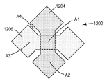
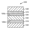
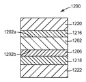
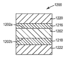
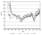
이제 도 12a 내지 도 12f를 참조하면, 본 발명의 양태에 따른 다층 구조의 예시적인 실시예의 여러 영역에서 측정된 반사율은 다층 구조의 패터닝된 투명 도전층에 대한 나안 식별 불가능성의 수준을 나타낸다. 다층 구조(1200)는, 예를 들어, 도 1의 터치 감지 디바이스(110)와 같은 터치 감지 디바이스에 사용하기 위한 터치 센서일 수 있다. 도 12a 내지 도 12e를 참조하면, 다층 구조(1200)는 반대 방향의 두 측면을 가지며, 반대 방향의 두 주표면(1202a, 1202b)을 갖는 중심 중합체 UV 투명 기판(1202), 중심 중합체 UV 투명 기판(1202)의 제1 주표면(1202a) 상의 제1 투명 도전층(1204), 및 중심 중합체 UV 투명 기판(1202)의 제2 주표면(1202b) 상의 제2 투명 도전층(1206)을 포함한다. 제1 투명 도전층(1204)은 제1 세트의 전극을 형성하도록 패터닝되고, 제2 투명 도전층(1206)은 제2 세트의 전극을 형성하도록 패터닝된다. 다층 구조(1200)는 제1 투명 도전층(1204) 상에 배치되는 제1 접착제층(1216) 및 제2 투명 도전층(1206) 상에 배치되는 제2 접착제층(1218)을 추가로 포함한다. 제1 접착제 층(1216)은 제1 세트의 전극 및 제1 세트의 전극으로 커버되지 않은 중심 중합체 UV 투명 기판(1202)의 일부분을 실질적으로 커버하도록 배치되고, 제2 접착제 층(1218)은 제2 세트의 전극 및 제2 세트의 전극으로 커버되지 않은 중심 중합체 UV 투명 기판(1202)의 일부분을 실질적으로 커버하도록 배치된다. 다층 구조(1200)는 제1 접착제층(1216)에 부착되는 제1 하드 코트층(1220) 및 제2 접착제층(1218)에 부착되는 제2 하드 코트층을 추가로 포함한다. 도 12a는 제1 투명 도전층에 의해 형성되는 제1 세트의 전극의 일부분 및 제2 투명 도전층(1206)에 의해 형성되는 제2 세트의 전극의 일부분을 도시하는 다층 구조(1200)의 일부분의 평면도이다. 도 12b 내지 도 12e는 각각 영역 A1 내지 영역 A4 (도 12a)에서 취해진 다층 구조(1200)의 단면도이다. 중심 중합체 UV 투명 기판(1202)은 듀폰 테이진 필름으로부터 상표명 멜리넥스 ST 505(Melinex ST 505)로 입수가능한, 두께 약 125 μm이고 굴절률 약 1.63인 PET를 포함한다. 제1 투명 도전층(1204)은 두께가 23 nm인 제2 층의 ITO 상에 있는 알루미늄으로 도핑된 두께가 약 49 nm인 제1 층의 규소 산화물 상에 있는 두께가 23 nm인 제1 층의 ITO를 포함한다. 제2 투명 도전층(1206)은 두께가 23 nm인 제2 층의 ITO 상에 있는 알루미늄으로 도핑된 두께가 약 49 nm인 제1 층의 규소 산화물 상에 있는 두께가 23 nm인 제1 층의 ITO를 포함한다. 제1 접착제 층(1216)은 미국 미네소타 주, 쓰리엠 컴퍼니로부터 상표명 8142KCL으로 입수가능한, 두께가 약 50 μm이고 굴절률이 약 1.47인, 광학적 투명 접착제를 포함한다. 제2 접착제 층(1218)은 미국 미네소타 주, 쓰리엠 컴퍼니로부터 상표명 8271로 입수가능한, 두께가 약 25 μm이고 굴절률이 약 1.47인, 광학적 투명 접착제를 포함한다. 제1 하드 코트층(1220) 및 제2 하드 코트층(1222)은 각각 듀폰 테이진 필름으로부터 상표명 멜리넥스 ST 505로 입수가능한, 두께 약 125 μm인, PET를 포함한다. 대안적으로, 듀폰 테이진 필름으로부터 상표명 멜리넥스 ST 504로 입수가능한 PET, 또는 임의의 적합한 광학적 투명 열 안정형 PET가 사용될 수 있다. 일부 실시예에서, 하드 코트층은 각각 하드 코트가 있는 PET를 포함한다. 일부 실시예에서, 제1 하드 코트층(1220)은 유리를 포함하고 제2 하드 코트층(1222)은 이형 라이너를 포함하며, 일 양태에서는 경제적이고 얇은 조립체를 제공한다. 이형 라이너 제거 후, 다층 구조는 예를 들어, LCD 패널에 라미네이트될 수 있다. 도 12f에 도시된 바와 같이, 다층 구조(1200)의 다른 영역 및 적어도 약 400 nm 내지 약 800 nm 범위의 파장에서의 반사율은 약 1% 범위 내에 있다. 가시광 범위는 보라색, 대략 400 nm, 내지 진적색, 대략 700 nm,이기 때문에 이 측정들은 다층 구조의 패터닝된 투명 도전층에 대한 나안 식별 불가능성이 우수한 수준임을 나타낸다.
다음은 본 발명의 태양에 따른 방법의 예시적인 실시예들이다.
실시예 1은 방법으로서, 반대 방향의 두 측면을 갖고, 반대 방향의 두 주표면을 갖는 중심 중합체 UV 투명 기판, 상기 중합체 기판의 반대 방향의 각각의 두 주표면 상의 투명 도전층, 및 각각의 투명 도전층 상의 금속성 도전층을 포함하는 다층 구조를 제공하는 단계; 투명 도전층을 위한 원하는 패턴을 갖는 포토이미지 마스크를 형성하기 위하여 두 금속성 도전층 상에 제1 포토이미지(photoimage) 층을 도포하고 패터닝하는 단계; 금속성 도전층 및 투명 도전층 중에서 포토이미지 마스크에 의해 노출된 부분을 에칭하는 단계; 포토이미지 마스크를 제거하는 단계; 금속성 도전층을 위한 원하는 패턴을 갖는 포토이미지 마스크를 형성하기 위하여 각 금속성 도전층의 남은 부분 위에 제2 포토이미지 층을 도포하고 패터닝하는 단계; 및 금속성 도전층의 노출된 부분을 에칭하는 단계를 포함하는 방법이다.
실시예 2는 방법으로서, 반대 방향의 두 측면을 갖고, 반대 방향의 두 주표면을 갖는 중심 중합체 UV 투명 기판, 상기 중합체 기판의 반대 방향의 각각의 두 주표면 상의 투명 도전층, 및 각각의 투명 도전층 상의 금속성 도전층을 포함하는 다층 구조를 제공하는 단계; 투명 도전층 및 금속성 도전층을 위한 원하는 패턴을 갖는 포토이미지 마스크를 형성하기 위하여 두 금속성 도전층 상에 제1 포토이미지 층을 도포하고 패터닝하는 단계; 금속성 도전층 및 투명 도전층 중에서 포토이미지 마스크에 의해 노출된 부분을 에칭하는 단계; 포토이미지 마스크를 제거하는 단계; 금속성 도전층의 원하는 패턴을 보호하는 포토이미지 마스크를 형성하기 위하여 각 금속성 도전층의 남은 부분 위에 제2 포토이미지 층을 도포하고 패터닝하는 단계; 및 금속성 도전층의 노출된 부분을 에칭하는 단계를 포함하는 방법이다.
실시예 3은 실시예 1 또는 실시예 2에 있어서, 상기 중심 중합체 기판은 폴리에스테르, 폴리카보네이트, 액정 중합체, 폴리이미드, 및 폴리에틸렌 나프탈레이트로 구성된 그룹에서 선택되는, 방법이다.
실시예 4는 실시예 1 또는 실시예 2에 있어서, 상기 중심 가요성 기판은 폴리에틸렌 테레프탈레이트 (PET)를 포함하는, 방법이다.
실시예 5는 실시예 1 또는 실시예 2에 있어서, 상기 투명 도전층이 인듐 주석 산화물 (ITO)을 포함하는, 방법이다.
실시예 6은 실시예 5에 있어서, 상기 ITO가 비결정질인, 방법이다.
실시예 7은 실시예 1 또는 실시예 2에 있어서, 상기 투명 도전층은 ITO 및 규소 산화물 층을 포함하는, 방법이다.
실시예 8은 실시예 7에 있어서, 상기 규소 산화물은 알루미늄으로 도핑되는, 방법이다.
실시예 9는 실시예 1 또는 실시예 2에 있어서, 상기 다층 구조의 반대 방향의 측면 상의 상기 포토이미지 층은 UV 광에 동시에 노출되는, 방법이다.
실시예 10은 실시예 1 또는 실시예 2에 있어서, 상기 다층 구조의 반대 방향의 측면 상의 상기 금속성 도전층은 동시에 에칭되는, 방법이다.
실시예 11은 실시예 1 또는 실시예 2에 있어서, 상기 다층 구조의 반대 방향의 측면 상의 상기 투명 도전층은 동시에 에칭되는, 방법이다.
실시예 12는 실시예 1 또는 실시예 2에 있어서, 상기 금속성 도전층은 구리, 알루미늄, 금, 은, 니켈, 및 주석으로 구성된 그룹에서 선택되는, 방법이다.
실시예 13은 실시예 1 또는 실시예 2에 있어서, 상기 금속성 도전층 중에 하나 또는 둘 모두를 위한 원하는 패턴은 상기 투명 도전층을 디바이스에 연결하기 위한 회로를 포함하는, 방법이다.
실시예 14는 실시예 1 또는 실시예 2에 있어서, 상기 금속성 도전층의 노출된 부분은 ITO를 에칭하지 않는 에칭액으로 에칭되는, 방법이다.
실시예 15는 실시예 14에 있어서, 상기 에칭액은 암모니아 계열인, 방법이다.
실시예 16은 용품으로서, 반대 방향의 두 측면을 갖고 중심 중합체 UV 투명 기판, 상기 중합체 기판의 반대 방향의 각각의 두 주표면 상의 투명 도전층, 및 각각의 투명 도전층 상의 금속성 도전층을 포함하는 다층 구조를 포함하는, 용품이다.
실시예 17은 실시예 16에 있어서, 다층 구조는 각 금속성 도전층 상에 패터닝된 포토이미지 마스크를 추가로 포함하는, 용품이다.
실시예 18은 실시예 16에 있어서, 두 투명 도전층이 패터닝되는, 용품이다.
실시예 19는 실시예 18에 있어서, 두 금속성 도전층이 패터닝되는, 용품이다.
실시예 20은 실시예 19에 있어서, 상기 패터닝되는 금속성 도전층은 폭이 약 30 마이크로미터 내지 약 100 마이크로미터, 높이가 약 3 마이크로미터 내지 약 35 마이크로미터, 피치가 약 60 마이크로미터 내지 약 200 마이크로미터인 트레이스를 포함하는 회로를 포함하는, 용품이다.
실시예 21은 실시예 19로서, 상기 패터닝되는 금속성 도전층은 트레이스를 포함하는 회로를 포함하고, 상기 다층 구조의 한 측면 상의 상기 패터닝되는 금속성 도전층의 트레이스는 다층 구조의 다른 한 측면 상의 패터닝되는 금속성 도전층의 트레이스로부터 상쇄(offset)되어 상기 트레이스가 기판 주표면의 평면에 수직한 방향으로 중첩되지 않도록 하는, 용품이다.
실시예 22는 실시예 16에 있어서, 상기 중심 중합체 기판은 폴리에스테르, 폴리카보네이트, 액정 중합체, 폴리이미드, 및 폴리에틸렌 나프탈레이트로 구성된 그룹에서 선택되는, 방법이다.
실시예 23은 실시예 16에 있어서, 상기 중심 중합체 기판은 폴리에틸렌 테레프탈레이트 (PET)를 포함하는, 용품이다.
실시예 24는 실시예 16에 있어서, 상기 투명 도전층이 인듐 주석 산화물 (ITO)을 포함하는, 용품이다.
실시예 25는 실시예 24에 있어서, 상기 ITO가 비결정질인, 용품이다.
실시예 26은 실시예 16에 있어서, 상기 투명 도전층은 ITO 및 규소 산화물 층을 포함하는, 용품이다.
실시예 27은 실시예 26에 있어서, 상기 규소 산화물은 알루미늄으로 도핑되는, 용품이다.
실시예 28은 실시예 16에 있어서, 상기 금속성 도전층은 구리, 알루미늄, 및 금으로 구성되는 그룹에서 선택되는, 용품이다.
실시예 29는 실시예 16에 있어서, 상기 다층 구조는 비-터치 감지 영역 및 적어도 하나의 비-터치 감지 영역으로부터 연장되는 종방향 커넥터 테일(connector tail)을 포함하는, 용품이다.
실시예 30은 용품으로서, 반대 방향의 두 측면을 갖고, 반대 방향의 주표면을 갖는 중심 중합체 UV 투명 기판, 및 상기 기판의 반대 방향의 주표면 상의 패터닝된 투명 도전층을 포함하는 다층 구조를 포함하고, 상기 중합체 UV 투명 기판의 굴절률은 약 1.60을 초과하는, 용품이다.
실시예 31은 실시예 30에 있어서, 상기 중합체 UV 투명 기판의 굴절률은 약 1.63을 초과하는, 용품이다.
실시예 32는 실시예 30에 있어서, 두 투명 도전층 상에 패터닝된 금속성 도전층을 추가로 포함하는, 용품이다.
실시예 33은 실시예 32에 있어서, 상기 패터닝되는 금속성 도전층은 폭이 약 30 마이크로미터 내지 약 100 마이크로미터, 높이가 약 3 마이크로미터 내지 약 35 마이크로미터, 피치가 약 60 마이크로미터 내지 약 200 마이크로미터인 트레이스를 포함하는 회로를 포함하는, 용품이다.
실시예 34는 실시예 32로서, 상기 패터닝되는 금속성 도전층은 트레이스를 포함하는 회로를 포함하고, 상기 다층 구조의 한 측면 상의 상기 패터닝되는 금속성 도전층의 트레이스는 다층 구조의 다른 한 측면 상의 패터닝되는 금속성 도전층의 트레이스로부터 상쇄(offset)되어 상기 트레이스가 기판 주표면의 평면에 수직한 방향으로 중첩되지 않도록 하는, 용품이다.
달리 언급하지 않는 한, 본 명세서 및 특허청구범위에 사용되는 양, 특성의 측정치 등을 표현하는 모든 숫자는 "약"이라는 용어에 의해 수식되는 것으로 이해되어야 한다. 그에 따라, 달리 언급하지 않는 한, 명세서 및 특허청구범위에 기술되는 숫자 파라미터는 본 출원의 개시 내용을 이용하여 당업자가 달성하고자 하는 원하는 특성에 따라 다를 수 있는 근사치이다. 특허청구범위의 범주에 대한 등가물의 원칙의 적용을 제한하려고 시도함이 없이, 각각의 수치적 파라미터는 적어도 보고된 유효 숫자의 수의 관점에서 그리고 통상의 반올림 기법을 적용하여 해석되어야 한다. 본 발명의 넓은 범주를 기술하는 수치 범위 및 파라미터가 근사치임에도 불구하고, 임의의 수치 값이 본 명세서에 설명된 특정 예에 기술되는 한, 이들은 가능한 한 합리적으로 정확히 보고된다. 그러나, 임의의 수치 값은 시험 또는 측정 한계와 관련된 오차를 분명히 포함할 수 있다.
특정 실시예가 바람직한 실시예의 설명을 목적으로 본 명세서에서 도시되고 설명되었지만, 동일한 목적을 달성하기에 적합한 매우 다양한 대안의 및/또는 등가의 구현예가 본 발명의 범주로부터 벗어남이 없이 도시되고 설명된 특정 실시예를 대신할 수 있다는 것이 당업자에 의해 이해될 것이다. 기계, 광학, 및 전기 분야의 당업자는 본 발명이 매우 광범위하게 다양한 실시 형태들로 구현될 수 있음을 쉽게 인식할 것이다. 본 출원은 본 명세서에서 논의된 양호한 실시예의 임의의 적응 또는 변경을 포함하도록 의도된다. 따라서, 본 발명은 오직 청구의 범위 및 그의 등가물에 의해서만 한정되는 것으로 명시적으로 의도된다.≪ 1 >
1 is a schematic plan view of an exemplary embodiment of a touch sensing device and an electronic device according to an aspect of the present invention.
2,
2 is a cross-sectional view of an exemplary embodiment of a multi-layer structure in accordance with an aspect of the present invention.
3A,
Figures 3A-3B are top and cross-sectional views, respectively, of an exemplary embodiment of a multi-layer structure in accordance with an aspect of the present invention.
<Fig. 4>
4 is a cross-sectional view of an exemplary embodiment of a multi-layer structure in accordance with an aspect of the present invention.
5,
5 is a cross-sectional view of an exemplary embodiment of a multi-layer structure in accordance with an aspect of the present invention.
6,
6 is a cross-sectional view of an exemplary embodiment of a multi-layer structure in accordance with an aspect of the present invention.
7A to 7B,
7A-7B are top and cross-sectional views, respectively, of an exemplary embodiment of a multi-layer structure in accordance with an aspect of the present invention.
≪ Figures 8A to 8E &
8A-8E are schematic plan views of an exemplary embodiment of a multi-layer structure according to various aspects of the present invention.
9,
9 is a cross-sectional view of an exemplary embodiment of a multi-layer structure in accordance with an aspect of the present invention.
<Fig. 10a>
10A-I are cross-sectional views of steps of an exemplary method of making a multi-layer structure in accordance with an aspect of the present invention.
11)
11 is a cross-sectional view of an exemplary embodiment of a multi-layer structure in accordance with an aspect of the present invention.
12A,
12A-12F are top, cross-sectional, and reflectance graphs of an exemplary embodiment of a multi-layer structure in accordance with an aspect of the present invention.
In the drawings, the same reference numerals designate the same elements.
DETAILED DESCRIPTION OF THE INVENTION [
In the following detailed description of the preferred embodiments, reference is made to the accompanying drawings which form a part hereof. BRIEF DESCRIPTION OF THE DRAWINGS The accompanying drawings illustrate, by way of example, specific embodiments in which the invention may be practiced. It is to be understood that other embodiments may be utilized and structural or logical changes may be made without departing from the scope of the present invention. The following detailed description is, therefore, not to be taken in a limiting sense, and the scope of the present invention is to be determined by the appended claims.
At least some embodiments of the present invention include a matrix type electrode comprising a row electrode and a column electrode on opposite sides of the substrate. This can eliminate the need for two substrate layers with transparent electrodes, an optical transparent adhesive, and a lamination process. Also, in at least some embodiments of the present invention, for example, conductive bus bars and bonding pads crowded at fine pitches are provided for connecting transparent electrodes to a controller unit. The fine pitch conductive bus bars along the edge of the transparent electrode reduce the non-touch-sensing area and eliminate the need for large individual connectors, expensive individual FPCs, ACFs for bonding to transparent electrodes, conductive ink printing, and heating processes. Compared to conductive ink printing, a conductive bus bar with a substantially vertical wall and an optimized top surface area can be obtained. Embodiments of the present invention may, for example, provide a high transmittance of greater than about 87% and a low turbidity of, for example, less than 1%. Because of the ability to provide relatively thick conductive bus bars, embodiments of the present invention can provide low resistance and high signal response.
The electrode pattern may be implemented as a bar, triangle, honeycomb, or any other suitable pattern. The transparent electrode may be coupled to an electronic component that determines the coordinates of the touch or proximity touch by sensing a change in capacitance between the electrodes, or capacitance between the electrodes and the ground.
1 illustrates an exemplary embodiment of a touch sensing device and an electronic device according to an aspect of the present invention. The
Although the
The capacitive coupling between any row and column electrodes is primarily a function of the geometry of the electrodes in the region where the electrodes are closest to each other. This region corresponds to a "node" of the electrode matrix, some of which are shown in Fig. For example, capacitive coupling between
When the user's
The
The controller may also include circuitry to store charge from a series of response signal inputs. An exemplary circuit device for this may include one or more capacitors, for example one or more capacitors, and selects it according to the characteristics of the drive signal and the corresponding response signal. Each pulse results in the accumulation of some quantum of charge, and each additional pulse is added in succession. The charge can also be coupled in only one cycle, and any additional pulses can only enable the averaging of the charge for noise reduction. The controller may also include one or more analog-to-digital converters (ADCs) for converting the analog amplitude of the stored signal into a digital format. One or more multiplexers may also be used to avoid redundancy of unnecessary circuit elements. Of course, the controller also preferably includes one or more memory devices that store the measured amplitude and associated parameters, and a microprocessor that performs the necessary computation and control functions.
By measuring the voltage of the accumulated charge associated with the response signal for each node in the electrode matrix for one or more pulses associated with an arbitrary measurement cycle, the controller calculates a matrix of measured values associated with the associated capacitance for each node of the electrode matrix Can be made. To determine which node (if any) experiences a change in coupling capacitance due to the presence of a touch, these measured values may be compared to a similar matrix of previously obtained reference values.
Figure 2 illustrates an exemplary embodiment of a multi-layer structure in accordance with an aspect of the present invention. In one aspect, the
3A and 3B illustrate another exemplary embodiment of a multi-layer structure according to an aspect of the present invention. The
Figure 4 illustrates another exemplary embodiment of a multi-layer structure in accordance with an aspect of the present invention. The
Figure 5 illustrates another exemplary embodiment of a multi-layer structure in accordance with an aspect of the present invention. The
Figure 6 illustrates another exemplary embodiment of a multi-layer structure in accordance with an aspect of the present invention. The
7A-7B illustrate another exemplary embodiment of a multi-layer structure in accordance with aspects of the present invention. The
As is appropriate for the intended application, the one or more connector tails may extend from the multi-layered non-touch sensitive area at any suitable location. 8A-8E illustrate an exemplary embodiment of a multi-layer structure in accordance with various aspects of the present invention, and various exemplary connector tail configurations are shown. 8A, the
In some embodiments, the conductive circuits of the non-touch sensitive area and / or the multi-layered connector tail are protected by a protective layer. Providing a protective layer may, for example, prevent corrosion and physical damage to the conductive circuit. Figure 9 illustrates an exemplary embodiment of a multi-layer structure according to an aspect of the present invention including such a protective layer. The multi-layer structure 900 may be, for example, a touch sensor for use with a touch sensing device, such as the
Creating a multi-layer structure according to various aspects of the present invention may be performed in various ways. It includes applying and patterning the photoimage layer and etching the underlying layer. The benefits of the method of making a multi-layer structure according to various aspects of the present invention include a high yield due to good interlayer deposition, for example, three layers of an exemplary structure according to embodiments of the present invention in five layers of an exemplary conventional structure Reduced number of layers, reduced number of process steps, and reduced production costs. In addition, a method of forming a multilayer structure according to various aspects of the present invention can prevent air bubbles and foreign substances between transparent conductive layers, prevent slippage between transparent conductive layers, for example, by using PET as a dielectric medium, A thin multilayer structure can be made and a patterned transparent conductive layer can provide a structure that is not identifiable inside. 10A-I illustrate steps of an exemplary method of making a multi-layer structure in accordance with an aspect of the present invention.
Referring to FIG. 10A, a
Referring to FIGS. 10B to 10C, first photo image layers 1040 and 1042 are applied (FIG. 10B) and patterned on two metallic conductive layers to form a photoimage mask having a desired pattern for the transparent conductive layer (Fig. 10C). In another method, the photoimage mask has a desired pattern for the transparent conductive layer and the metallic conductive layer. The
10D, the first metallic
Referring to FIG. 10E, the photo image mask is removed. This can be done by placing the
10F-10G, a
Referring to FIG. 10H, the exposed portions of the first metallic
Referring to FIG. 10I, the photo image mask is removed. This can be done by placing the
11 illustrates an exemplary embodiment in which the patterned transparent conductive layer is refractive index matched to at least the central polymer UV transparent substrate. As a result, the pattern of the patterned transparent conductive layer is not identifiable as it is. In one aspect, the
Referring now to Figures 12A-12F, the measured reflectivity in various regions of an exemplary embodiment of a multi-layer structure in accordance with an embodiment of the present invention represents a level of unclear discernibility for a patterned transparent conductive layer in a multi-layer structure. The
The following are exemplary embodiments of the method according to an aspect of the present invention.
Example 1 is a method comprising, as a method, a process comprising the steps of: providing a central polymer UV transparent substrate having two opposite sides and having two major surfaces in opposite directions, a transparent conductive layer on each of the two major surfaces in the opposite direction of the polymer substrate, Providing a multilayer structure comprising a metallic conductive layer on the conductive layer; Applying and patterning a first photoimage layer on the two metallic conductive layers to form a photoimage mask having a desired pattern for the transparent conductive layer; Etching the exposed portions of the metallic conductive layer and the transparent conductive layer by a photoimage mask; Removing the photo image mask; Applying and patterning a second photoimage layer over a remaining portion of each metallic conductive layer to form a photoimage mask having a desired pattern for the metallic conductive layer; And etching the exposed portions of the metallic conductive layer.
Example 2 is a method comprising, as a method, a process comprising the steps of: forming a central polymer UV transparent substrate having two opposite sides and having two major surfaces in opposite directions, a transparent conductive layer on each of the two major surfaces in the opposite direction of the polymer substrate, Providing a multilayer structure comprising a metallic conductive layer on the conductive layer; Applying and patterning a first photoimage layer on the two metallic conductive layers to form a photoimage mask having a desired pattern for the transparent conductive layer and the metallic conductive layer; Etching the exposed portions of the metallic conductive layer and the transparent conductive layer by a photoimage mask; Removing the photo image mask; Applying and patterning a second photoimage layer over a remaining portion of each metallic conductive layer to form a photoimage mask protecting the desired pattern of metallic conductive layer; And etching the exposed portions of the metallic conductive layer.
Example 3 is a method in Example 1 or Example 2 wherein the central polymer substrate is selected from the group consisting of polyester, polycarbonate, liquid crystal polymer, polyimide, and polyethylene naphthalate.
Embodiment 4 is a method according to Embodiment 1 or Embodiment 2, wherein the central flexible substrate comprises polyethylene terephthalate (PET).
Embodiment 5 is a method in Embodiment 1 or Embodiment 2, wherein the transparent conductive layer comprises indium tin oxide (ITO).
Example 6 is a method in Example 5 wherein the ITO is amorphous.
Example 8 is a method in Example 7 wherein the silicon oxide is doped with aluminum.
Example 9 is a method according to Example 1 or Example 2 wherein the photoimage layer on the opposite side of the multilayer structure is simultaneously exposed to UV light.
Example 11 is a method in which in Example 1 or Example 2, the transparent conductive layer on the side in the opposite direction of the multi-layer structure is simultaneously etched.
Example 14 is a method in which in Example 1 or Example 2, the exposed portion of the metallic conductive layer is etched with an etchant that does not etch ITO.
Example 15 is a method in Example 14 wherein the etching solution is ammonia-based.
Example 16 is an electrophotographic photoconductor comprising as an article a photoconductive layer comprising a central polymeric UV transparent substrate having two sides in opposing directions, a transparent conductive layer on each of the two major surfaces in the opposite direction of the polymeric substrate, and a metallic conductive layer on each transparent conductive layer Comprising a multi-layer structure.
Example 17 is an article according to Example 16, wherein the multilayer structure further comprises a patterned photoimage mask on each metallic conductive layer.
Example 18 is an article in Example 16 in which two transparent conductive layers are patterned.
Example 19 is an article in Example 18 in which two metallic conductive layers are patterned.
Example 20 is similar to Example 19 wherein the metallic conductive layer to be patterned has a width of about 30 micrometers to about 100 micrometers, a height of about 3 micrometers to about 35 micrometers, a pitch of about 60 micrometers to about 200 micrometers And a circuit including a trace, which is a micrometer.
Example 21 is Example 19 wherein the patterned metallic conductive layer comprises a circuit comprising a trace and the trace of the patterned metallic conductive layer on one side of the multilayer structure is patterned on the other side of the multi- And offset from the traces of the metallic conductive layer such that the traces do not overlap in a direction perpendicular to the plane of the major surface of the substrate.
Example 22 is the method as in Example 16 wherein the central polymer substrate is selected from the group consisting of polyester, polycarbonate, liquid crystal polymer, polyimide, and polyethylene naphthalate.
Example 23 is an article according to example 16 wherein the central polymer substrate comprises polyethylene terephthalate (PET).
Example 24 is an article according to Example 16 wherein the transparent conductive layer comprises indium tin oxide (ITO).
Example 25 is an article in which the ITO is amorphous in Example 24.
Example 26 is an article according to Example 16 wherein the transparent conductive layer comprises ITO and a silicon oxide layer.
Example 27 is an article according to example 26 wherein the silicon oxide is doped with aluminum.
Example 28 is the article of embodiment 16 wherein the metallic conductive layer is selected from the group consisting of copper, aluminum, and gold.
Embodiment 29. The article of embodiment 16, wherein the multilayer structure comprises a longitudinal connector tail extending from a non-touch sensitive area and at least one non-touch sensitive area.
Example 30 comprises as an article a multilayer structure comprising a central polymer UV transparent substrate having two opposite sides in the opposite direction and having a major surface in the opposite direction and a patterned transparent conductive layer on the major surface in the opposite direction of the substrate And the refractive index of the polymeric UV transparent substrate is greater than about 1.60.
Example 31 is an article according to example 30 wherein the refractive index of the polymeric UV transparent substrate is greater than about 1.63.
Example 32 is an article according to Example 30, further comprising a patterned metallic conductive layer on the two transparent conductive layers.
Example 33 is similar to embodiment 32 wherein the metallic conductive layer to be patterned has a width of about 30 micrometers to about 100 micrometers, a height of about 3 micrometers to about 35 micrometers, a pitch of about 60 micrometers to about 200 micrometers And a circuit including a trace, which is a micrometer.
Example 34 is Example 32 wherein the patterned metallic conductive layer comprises a circuit comprising a trace and the trace of the patterned metallic conductive layer on one side of the multilayer structure is patterned on the other side of the multi- And offset from the traces of the metallic conductive layer such that the traces do not overlap in a direction perpendicular to the plane of the major surface of the substrate.
Unless otherwise stated, all numbers expressing quantities, measurements of properties, etc., as used in this specification and the appended claims are to be understood as modified by the term "about ". Accordingly, unless indicated to the contrary, the numerical parameters set forth in the specification and claims are approximations that may vary depending upon the desired properties sought to be attained by those skilled in the art using the teachings of the present application. Without wishing to limit the application of the doctrine of equivalents to the scope of the claims, each numerical parameter should at least be construed in light of the number of reported significant digits and by applying ordinary rounding techniques. Notwithstanding that numerical ranges and parameters describing the broad scope of the invention are approximations, as long as any numerical value is described in the specific examples set forth herein, they are reported as reasonably and accurately as possible. However, any numerical value may explicitly include an error associated with the test or measurement limit.
While particular embodiments have been shown and described herein for purposes of description of the preferred embodiments, a wide variety of alternative and / or equivalent implementations suitable for achieving the same purpose may be made without departing from the scope of the present invention, It will be understood by those skilled in the art that the examples may be substituted. Those of ordinary skill in the mechanical, optical, and electrical arts will readily appreciate that the present invention can be implemented in a wide variety of different embodiments. This application is intended to cover any adaptations or variations of the preferred embodiments discussed herein. Accordingly, the present invention is expressly intended to be limited only by the claims and their equivalents.
Claims (15)
투명 도전층을 위한 원하는 패턴을 갖는 포토이미지 마스크를 형성하기 위하여 두 금속성 도전층 상에 제1 포토이미지(photoimage) 층을 도포하고 패터닝하는 단계;
금속성 도전층 및 투명 도전층 중에서 포토이미지 마스크에 의해 노출된 부분을 에칭하는 단계;
포토이미지 마스크를 제거하는 단계;
금속성 도전층을 위한 원하는 패턴을 갖는 포토이미지 마스크를 형성하기 위하여 각 금속성 도전층의 남은 부분 위에 제2 포토이미지 층을 도포하고 패터닝하는 단계; 및
금속성 도전층의 노출된 부분을 에칭하는 단계를 포함하는, 방법.A central polymeric UV transparent substrate having two opposite sides in opposite directions and having two major surfaces in opposite directions, a transparent conductive layer on each of the two major surfaces in the opposite direction of the polymer substrate, and a metallic conductive layer on each transparent conductive layer Providing a multi-layer structure comprising;
Applying and patterning a first photoimage layer on the two metallic conductive layers to form a photoimage mask having a desired pattern for the transparent conductive layer;
Etching the exposed portions of the metallic conductive layer and the transparent conductive layer by a photoimage mask;
Removing the photo image mask;
Applying and patterning a second photoimage layer over a remaining portion of each metallic conductive layer to form a photoimage mask having a desired pattern for the metallic conductive layer; And
Etching the exposed portion of the metallic conductive layer.
투명 도전층 및 금속성 도전층을 위한 원하는 패턴을 갖는 포토이미지 마스크를 형성하기 위하여 두 금속성 도전층 상에 제1 포토이미지 층을 도포하고 패터닝하는 단계;
금속성 도전층 및 투명 도전층 중에서 포토이미지 마스크에 의해 노출된 부분을 에칭하는 단계;
포토이미지 마스크를 제거하는 단계;
금속성 도전층의 원하는 패턴을 보호하는 포토이미지 마스크를 형성하기 위하여 각 금속성 도전층의 남은 부분 위에 제2 포토이미지 층을 도포하고 패터닝하는 단계; 및
금속성 도전층 중에서 노출된 부분을 에칭하는 단계를 포함하는, 방법.A central polymeric UV transparent substrate having two opposite sides in opposite directions and having two major surfaces in opposite directions, a transparent conductive layer on each of the two major surfaces in the opposite direction of the polymer substrate, and a metallic conductive layer on each transparent conductive layer Providing a multi-layer structure comprising;
Applying and patterning a first photoimage layer on the two metallic conductive layers to form a photoimage mask having a desired pattern for the transparent conductive layer and the metallic conductive layer;
Etching the exposed portions of the metallic conductive layer and the transparent conductive layer by a photoimage mask;
Removing the photo image mask;
Applying and patterning a second photoimage layer over a remaining portion of each metallic conductive layer to form a photoimage mask protecting the desired pattern of metallic conductive layer; And
And etching the exposed portions of the metallic conductive layer.
Applications Claiming Priority (3)
| Application Number | Priority Date | Filing Date | Title |
|---|---|---|---|
| US201161541563P | 2011-09-30 | 2011-09-30 | |
| US61/541,563 | 2011-09-30 | ||
| PCT/US2012/057415 WO2013049267A1 (en) | 2011-09-30 | 2012-09-27 | Flexible touch sensor with fine pitch interconnect |
Publications (1)
| Publication Number | Publication Date |
|---|---|
| KR20140072131A true KR20140072131A (en) | 2014-06-12 |
Family
ID=47996382
Family Applications (1)
| Application Number | Title | Priority Date | Filing Date |
|---|---|---|---|
| KR1020147011169A KR20140072131A (en) | 2011-09-30 | 2012-09-27 | Flexible touch sensor with fine pitch interconnect |
Country Status (6)
| Country | Link |
|---|---|
| US (1) | US9642243B2 (en) |
| JP (1) | JP6129185B2 (en) |
| KR (1) | KR20140072131A (en) |
| CN (1) | CN103827791B (en) |
| TW (1) | TWI588719B (en) |
| WO (1) | WO2013049267A1 (en) |
Cited By (2)
| Publication number | Priority date | Publication date | Assignee | Title |
|---|---|---|---|---|
| US9857845B2 (en) | 2015-09-21 | 2018-01-02 | Samsung Display Co., Ltd. | Flexible electronic device |
| KR102575205B1 (en) * | 2023-01-17 | 2023-09-08 | 주식회사 아이티에스솔루션 | All-in-one touch screen panel and bezel applied sensor device |
Families Citing this family (22)
| Publication number | Priority date | Publication date | Assignee | Title |
|---|---|---|---|---|
| WO2014145770A2 (en) * | 2013-03-15 | 2014-09-18 | Cirque Corporation | Flying sense electrodes for creating a secure cage for integrated circuits and pathways |
| WO2014204206A1 (en) | 2013-06-20 | 2014-12-24 | Lg Electronics Inc. | Conductive film and touch panel including the same |
| US20150052747A1 (en) * | 2013-08-22 | 2015-02-26 | Chih-Chung Lin | Manufacturing method of touch substrate |
| CN103472964A (en) * | 2013-09-07 | 2013-12-25 | 向火平 | Flexible capacitive screen and production process thereof |
| US9904386B2 (en) * | 2014-01-23 | 2018-02-27 | 3M Innovative Properties Company | Method for patterning a microstructure |
| WO2016028454A1 (en) | 2014-08-18 | 2016-02-25 | 3M Innovative Properties Company | Conductive layered structure and methods of making same |
| CN106716253B (en) * | 2014-09-22 | 2018-11-27 | 富士胶片株式会社 | The manufacturing method of the laminate of coating is plated containing pattern-like |
| CN104553113A (en) * | 2014-12-11 | 2015-04-29 | 业成光电(深圳)有限公司 | Acoustic wave fingerprint identification component and manufacturing method thereof |
| TWI536222B (en) * | 2014-12-12 | 2016-06-01 | 群創光電股份有限公司 | Touch device and touch display apparatus |
| US9489097B2 (en) * | 2015-01-23 | 2016-11-08 | Sony Corporation | Dynamic touch sensor scanning for false border touch input detection |
| KR102312314B1 (en) * | 2015-01-28 | 2021-10-13 | 삼성디스플레이 주식회사 | Touch sensor device and manufacturing method |
| CN105843438A (en) * | 2015-01-30 | 2016-08-10 | 启耀光电股份有限公司 | Electronic device and method for manufacturing electronic device |
| KR102320639B1 (en) * | 2015-02-04 | 2021-11-02 | 삼성디스플레이 주식회사 | Touch screen pannel and manufacturing method thereof |
| KR102322084B1 (en) * | 2015-04-30 | 2021-11-04 | 삼성디스플레이 주식회사 | Touch sensor device and manufacturing method |
| US9857930B2 (en) * | 2015-12-16 | 2018-01-02 | 3M Innovative Properties Company | Transparent conductive component with interconnect circuit tab comprising cured organic polymeric material |
| JP2019506673A (en) * | 2016-01-21 | 2019-03-07 | スリーエム イノベイティブ プロパティズ カンパニー | Multi-size touch sensor |
| KR20180054069A (en) * | 2016-11-14 | 2018-05-24 | 삼성전자주식회사 | Fingerprint sensor and method of manufacturing the same |
| KR102075065B1 (en) * | 2017-02-16 | 2020-02-07 | 동우 화인켐 주식회사 | Touch sensor and method of manufacturing the same |
| CN108574158B (en) * | 2017-03-14 | 2020-10-09 | 群创光电股份有限公司 | Display device and method for manufacturing the same |
| DE102019115946A1 (en) * | 2019-06-12 | 2020-12-31 | Preh Gmbh | Input device with movable handle on a capacitive detection surface and capacitive coupling devices |
| CN110489017B (en) * | 2019-09-27 | 2022-08-30 | 业成科技(成都)有限公司 | Touch screen, touch display screen and intelligent terminal |
| KR20220095552A (en) * | 2020-12-30 | 2022-07-07 | 엘지디스플레이 주식회사 | Display panel and display device |
Family Cites Families (35)
| Publication number | Priority date | Publication date | Assignee | Title |
|---|---|---|---|---|
| US3526504A (en) | 1966-07-07 | 1970-09-01 | Du Pont | Photocrosslinkable elements and processes |
| US3448098A (en) | 1966-09-27 | 1969-06-03 | Merck & Co Inc | Production of guanylic acid |
| US3469982A (en) | 1968-09-11 | 1969-09-30 | Jack Richard Celeste | Process for making photoresists |
| US3867153A (en) | 1972-09-11 | 1975-02-18 | Du Pont | Photohardenable element |
| US4733222A (en) | 1983-12-27 | 1988-03-22 | Integrated Touch Arrays, Inc. | Capacitance-variation-sensitive touch sensing array system |
| FR2658675B1 (en) | 1990-02-19 | 1994-09-16 | Techniphone | CAPACITIVE TYPE TOUCH SCREEN DEVICE. |
| JPH0769767B2 (en) | 1991-10-16 | 1995-07-31 | インターナショナル・ビジネス・マシーンズ・コーポレイション | Touch overlay for detecting finger touch or stylus position, and detection system |
| DE69324067T2 (en) | 1992-06-08 | 1999-07-15 | Synaptics Inc | Object position detector |
| US5840402A (en) * | 1994-06-24 | 1998-11-24 | Sheldahl, Inc. | Metallized laminate material having ordered distribution of conductive through holes |
| US7663607B2 (en) | 2004-05-06 | 2010-02-16 | Apple Inc. | Multipoint touchscreen |
| US6387600B1 (en) | 1999-08-25 | 2002-05-14 | Micron Technology, Inc. | Protective layer during lithography and etch |
| US6356337B1 (en) | 2000-03-08 | 2002-03-12 | Anvik Corporation | Two-sided substrate imaging using single-approach projection optics |
| US6518083B2 (en) * | 2001-01-31 | 2003-02-11 | Nippon Telegraph And Telephone Corporation | Surface shape recognition sensor and method of manufacturing the same |
| US20020117672A1 (en) | 2001-02-23 | 2002-08-29 | Ming-Sung Chu | High-brightness blue-light emitting crystalline structure |
| EP1491852A4 (en) | 2003-02-17 | 2011-08-31 | Nippon Telegraph & Telephone | Surface shape recognition sensor and method of producing the same |
| US7081888B2 (en) | 2003-04-24 | 2006-07-25 | Eastman Kodak Company | Flexible resistive touch screen |
| US8068186B2 (en) | 2003-10-15 | 2011-11-29 | 3M Innovative Properties Company | Patterned conductor touch screen having improved optics |
| US7351519B2 (en) | 2004-11-23 | 2008-04-01 | Advantech Global, Ltd | Patterning of indium-tin oxide (ITO) for precision-cutting and aligning a liquid crystal display (LCD) panel |
| US7439962B2 (en) | 2005-06-01 | 2008-10-21 | Synaptics Incorporated | Touch pad with flexible substrate |
| US7450296B2 (en) | 2006-01-30 | 2008-11-11 | Taiwan Semiconductor Manufacturing Company, Ltd. | Method and system for patterning alignment marks on a transparent substrate |
| JP5118309B2 (en) * | 2006-03-10 | 2013-01-16 | グンゼ株式会社 | Manufacturing method of film with transparent electrode and touch panel using film with transparent electrode |
| WO2007144993A1 (en) | 2006-06-12 | 2007-12-21 | Sharp Kabushiki Kaisha | Touch panel, display device and touch panel manufacturing method |
| JP5063500B2 (en) | 2008-02-08 | 2012-10-31 | 富士通コンポーネント株式会社 | Panel-type input device, method for manufacturing panel-type input device, and electronic apparatus including panel-type input device |
| US8629841B2 (en) | 2008-04-30 | 2014-01-14 | Apple Inc. | Multi-touch sensor patterns and stack-ups |
| JP5788129B2 (en) * | 2008-07-18 | 2015-09-30 | 日東電工株式会社 | Transparent conductive film and touch panel |
| TWI459436B (en) * | 2008-10-27 | 2014-11-01 | Tpk Touch Solutions Inc | The Method of Making Double - sided Graphic Structure of Touch Circuit |
| JP4958020B2 (en) | 2009-03-31 | 2012-06-20 | 大日本印刷株式会社 | Touch panel sensor, laminate for manufacturing touch panel sensor, and method for manufacturing touch panel sensor |
| US9417739B2 (en) | 2009-05-29 | 2016-08-16 | 3M Innovative Properties Company | High speed multi-touch touch device and controller therefor |
| KR20120117762A (en) | 2009-11-27 | 2012-10-24 | 도판 인사츠 가부시키가이샤 | Transparent conductive laminate, method for producing same, and electrostatic capacitance type touch panel |
| US8730184B2 (en) | 2009-12-16 | 2014-05-20 | 3M Innovative Properties Company | Touch sensitive device with multilayer electrode having improved optical and electrical performance |
| JP5471543B2 (en) * | 2010-02-09 | 2014-04-16 | 大日本印刷株式会社 | Touch panel sensor manufacturing method and touch panel sensor |
| JP5413228B2 (en) | 2010-02-09 | 2014-02-12 | 大日本印刷株式会社 | Touch panel sensor manufacturing method and touch panel sensor |
| JP5263277B2 (en) * | 2010-12-03 | 2013-08-14 | 大日本印刷株式会社 | Touch panel sensor, laminate for manufacturing touch panel sensor, and method for manufacturing touch panel sensor |
| CN102096535A (en) * | 2010-12-31 | 2011-06-15 | 晟光科技股份有限公司 | Manufacture method of capacitive touch screen |
| SG187274A1 (en) | 2011-07-14 | 2013-02-28 | 3M Innovative Properties Co | Etching method and devices produced using the etching method |
-
2012
- 2012-09-27 KR KR1020147011169A patent/KR20140072131A/en not_active Application Discontinuation
- 2012-09-27 JP JP2014533698A patent/JP6129185B2/en active Active
- 2012-09-27 WO PCT/US2012/057415 patent/WO2013049267A1/en active Application Filing
- 2012-09-27 CN CN201280047232.1A patent/CN103827791B/en not_active Expired - Fee Related
- 2012-09-27 US US14/240,815 patent/US9642243B2/en not_active Expired - Fee Related
- 2012-09-28 TW TW101136110A patent/TWI588719B/en not_active IP Right Cessation
Cited By (3)
| Publication number | Priority date | Publication date | Assignee | Title |
|---|---|---|---|---|
| US9857845B2 (en) | 2015-09-21 | 2018-01-02 | Samsung Display Co., Ltd. | Flexible electronic device |
| US10353434B2 (en) | 2015-09-21 | 2019-07-16 | Samsung Display Co., Ltd. | Flexible electronic device |
| KR102575205B1 (en) * | 2023-01-17 | 2023-09-08 | 주식회사 아이티에스솔루션 | All-in-one touch screen panel and bezel applied sensor device |
Also Published As
| Publication number | Publication date |
|---|---|
| WO2013049267A1 (en) | 2013-04-04 |
| TW201319905A (en) | 2013-05-16 |
| JP2014534458A (en) | 2014-12-18 |
| CN103827791B (en) | 2017-08-29 |
| CN103827791A (en) | 2014-05-28 |
| US9642243B2 (en) | 2017-05-02 |
| JP6129185B2 (en) | 2017-05-17 |
| US20140299365A1 (en) | 2014-10-09 |
| TWI588719B (en) | 2017-06-21 |
Similar Documents
| Publication | Publication Date | Title |
|---|---|---|
| JP6129185B2 (en) | Flexible contact sensor with fine pitch interconnection | |
| US9939954B2 (en) | Touch panel | |
| US9116584B2 (en) | Dielectric layer for touch sensor stack | |
| US9395836B2 (en) | System and method for reducing borders of a touch sensor | |
| EP2278438B1 (en) | Contact sensing device with improved edge position recognition characteristics | |
| TWI559197B (en) | Touch screen panel and method of fabricating the same | |
| US9911550B2 (en) | Touch sensitive device with multiple ablation fluence values | |
| CN111338496B (en) | Ultrathin touch sensor | |
| US9864463B2 (en) | Touch panel deformation compensation | |
| TWI420370B (en) | Touch panel sensor | |
| KR101690501B1 (en) | Touch panel sensor | |
| JP2012515392A (en) | Input device | |
| JP2006011523A (en) | Touch panel sensor | |
| KR101369054B1 (en) | Transparent conductive film | |
| US9098152B2 (en) | Dielectric layer for touch sensor stack | |
| KR20160096267A (en) | Touch screen pannel and manufacturing method thereof | |
| US20230376141A1 (en) | Input sensing unit and display device including the same | |
| KR20150000473A (en) | Touch panel sensor | |
| KR101219741B1 (en) | Touch panel including a conduction layer having lines | |
| JP7321112B2 (en) | Touch panel and display device provided with the same | |
| CN117055757A (en) | Ultrathin touch sensor | |
| JP2016194751A (en) | Touch panel sensor | |
| KR20120062652A (en) | Touch panel including a conduction layer having lines | |
| KR20160043816A (en) | Touch Sensor Module |
Legal Events
| Date | Code | Title | Description |
|---|---|---|---|
| E902 | Notification of reason for refusal | ||
| E601 | Decision to refuse application |