KR20140070399A - Data writer with tapered side shield sidewalls - Google Patents
Data writer with tapered side shield sidewalls Download PDFInfo
- Publication number
- KR20140070399A KR20140070399A KR1020130143035A KR20130143035A KR20140070399A KR 20140070399 A KR20140070399 A KR 20140070399A KR 1020130143035 A KR1020130143035 A KR 1020130143035A KR 20130143035 A KR20130143035 A KR 20130143035A KR 20140070399 A KR20140070399 A KR 20140070399A
- Authority
- KR
- South Korea
- Prior art keywords
- shield
- tip
- write pole
- pole
- magnetic
- Prior art date
Links
- 239000010410 layer Substances 0.000 description 14
- 238000013500 data storage Methods 0.000 description 12
- 238000010586 diagram Methods 0.000 description 11
- 239000000463 material Substances 0.000 description 8
- 238000003860 storage Methods 0.000 description 7
- 230000004907 flux Effects 0.000 description 5
- 238000004519 manufacturing process Methods 0.000 description 5
- 238000003475 lamination Methods 0.000 description 4
- 230000005415 magnetization Effects 0.000 description 3
- 230000015572 biosynthetic process Effects 0.000 description 2
- 238000006243 chemical reaction Methods 0.000 description 2
- 230000000694 effects Effects 0.000 description 2
- 230000002463 transducing effect Effects 0.000 description 2
- 230000006978 adaptation Effects 0.000 description 1
- 230000003542 behavioural effect Effects 0.000 description 1
- 230000001419 dependent effect Effects 0.000 description 1
- 230000001747 exhibiting effect Effects 0.000 description 1
- 239000011810 insulating material Substances 0.000 description 1
- 238000007885 magnetic separation Methods 0.000 description 1
- 238000005457 optimization Methods 0.000 description 1
- 238000009738 saturating Methods 0.000 description 1
- 230000035945 sensitivity Effects 0.000 description 1
- 239000002356 single layer Substances 0.000 description 1
- 230000007704 transition Effects 0.000 description 1
Images


Classifications
-
- G—PHYSICS
- G11—INFORMATION STORAGE
- G11B—INFORMATION STORAGE BASED ON RELATIVE MOVEMENT BETWEEN RECORD CARRIER AND TRANSDUCER
- G11B5/00—Recording by magnetisation or demagnetisation of a record carrier; Reproducing by magnetic means; Record carriers therefor
- G11B5/127—Structure or manufacture of heads, e.g. inductive
- G11B5/187—Structure or manufacture of the surface of the head in physical contact with, or immediately adjacent to the recording medium; Pole pieces; Gap features
-
- G—PHYSICS
- G11—INFORMATION STORAGE
- G11C—STATIC STORES
- G11C11/00—Digital stores characterised by the use of particular electric or magnetic storage elements; Storage elements therefor
- G11C11/02—Digital stores characterised by the use of particular electric or magnetic storage elements; Storage elements therefor using magnetic elements
- G11C11/14—Digital stores characterised by the use of particular electric or magnetic storage elements; Storage elements therefor using magnetic elements using thin-film elements
-
- B—PERFORMING OPERATIONS; TRANSPORTING
- B82—NANOTECHNOLOGY
- B82Y—SPECIFIC USES OR APPLICATIONS OF NANOSTRUCTURES; MEASUREMENT OR ANALYSIS OF NANOSTRUCTURES; MANUFACTURE OR TREATMENT OF NANOSTRUCTURES
- B82Y25/00—Nanomagnetism, e.g. magnetoimpedance, anisotropic magnetoresistance, giant magnetoresistance or tunneling magnetoresistance
-
- G—PHYSICS
- G11—INFORMATION STORAGE
- G11B—INFORMATION STORAGE BASED ON RELATIVE MOVEMENT BETWEEN RECORD CARRIER AND TRANSDUCER
- G11B5/00—Recording by magnetisation or demagnetisation of a record carrier; Reproducing by magnetic means; Record carriers therefor
- G11B5/127—Structure or manufacture of heads, e.g. inductive
- G11B5/31—Structure or manufacture of heads, e.g. inductive using thin films
- G11B5/3163—Fabrication methods or processes specially adapted for a particular head structure, e.g. using base layers for electroplating, using functional layers for masking, using energy or particle beams for shaping the structure or modifying the properties of the basic layers
-
- G—PHYSICS
- G11—INFORMATION STORAGE
- G11B—INFORMATION STORAGE BASED ON RELATIVE MOVEMENT BETWEEN RECORD CARRIER AND TRANSDUCER
- G11B5/00—Recording by magnetisation or demagnetisation of a record carrier; Reproducing by magnetic means; Record carriers therefor
- G11B5/127—Structure or manufacture of heads, e.g. inductive
- G11B5/33—Structure or manufacture of flux-sensitive heads, i.e. for reproduction only; Combination of such heads with means for recording or erasing only
- G11B5/39—Structure or manufacture of flux-sensitive heads, i.e. for reproduction only; Combination of such heads with means for recording or erasing only using magneto-resistive devices or effects
- G11B5/3903—Structure or manufacture of flux-sensitive heads, i.e. for reproduction only; Combination of such heads with means for recording or erasing only using magneto-resistive devices or effects using magnetic thin film layers or their effects, the films being part of integrated structures
- G11B5/3906—Details related to the use of magnetic thin film layers or to their effects
-
- G—PHYSICS
- G11—INFORMATION STORAGE
- G11B—INFORMATION STORAGE BASED ON RELATIVE MOVEMENT BETWEEN RECORD CARRIER AND TRANSDUCER
- G11B5/00—Recording by magnetisation or demagnetisation of a record carrier; Reproducing by magnetic means; Record carriers therefor
- G11B5/84—Processes or apparatus specially adapted for manufacturing record carriers
-
- H—ELECTRICITY
- H01—ELECTRIC ELEMENTS
- H01F—MAGNETS; INDUCTANCES; TRANSFORMERS; SELECTION OF MATERIALS FOR THEIR MAGNETIC PROPERTIES
- H01F41/00—Apparatus or processes specially adapted for manufacturing or assembling magnets, inductances or transformers; Apparatus or processes specially adapted for manufacturing materials characterised by their magnetic properties
- H01F41/14—Apparatus or processes specially adapted for manufacturing or assembling magnets, inductances or transformers; Apparatus or processes specially adapted for manufacturing materials characterised by their magnetic properties for applying magnetic films to substrates
- H01F41/22—Heat treatment; Thermal decomposition; Chemical vapour deposition
Abstract
Description
다양한 실시형태들은 일반적으로 높은 데이터 비트 밀도의 데이터 저장 환경들에서 사용될 수 있는 데이터 라이터에 관한 것이다.BACKGROUND OF THE INVENTION [0002] Various embodiments relate to data writers that can be used in data storage environments that generally have high data bit densities.
다양한 실시형태들에 따라, 기입 폴은 폴 측벽과, 리딩 및 트레일링 에지들을 연결하는 연속하는 제 1 테이퍼 각도를 가질 수도 있다. 기입 폴은, 쉴드 선단(shield tip)으로 테이퍼진 제 1 및 제 2 쉴드 측벽들로 구성된 사이드 쉴드 근처에 위치결정(position)될 수도 있으며, 쉴드 선단은 기입 폴과 사이드 쉴드 사이의 가장 근접한 지점이다.According to various embodiments, the write pole may have a pole sidewall and a successive first taper angle connecting the leading and trailing edges. The write pole may be positioned near a side shield comprising first and second shield side walls tapered to a shield tip and the shield tip is the closest point between the write pole and the side shield .
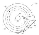
도 1은 다양한 실시형태들에 따라 구성되고(constructed) 동작되는 데이터 저장 디바이스의 예의 상측 관점 블록도이다.
도 2는 도 1의 데이터 저장 디바이스에 사용될 수 있는 자기 엘리먼트의 예의 단면 블록도를 도시한다.
도 3은 일부 실시형태들에 따라 구성된 자기 엘리먼트의 예의 일 부분의 ABS 관점 블록도를 나타낸다.
도 4는 다양한 실시형태들에 따라 구성된 자기 엘리먼트의 예의 일 부분의 ABS 관점 블록도를 보여준다.
도 5는 다양한 실시형태들에 따라 구성된 자기 엘리먼트의 예의 일 부분의 ABS 관점 블록도를 도시한다.
도 6은 일부 실시형태들에 따라 구성된 자기 엘리먼트의 예의 일 부분의 ABS 관점 블록도이다.
도 7은 다양한 실시형태들에 따라 수행된(conducted) 자기 엘리먼트 제조(fabrication) 루틴의 예에 대한 플로우차트를 제공한다.1 is a top perspective block diagram of an example of a data storage device constructed and operated in accordance with various embodiments.
Figure 2 shows a cross-sectional block diagram of an example of a magnetic element that may be used in the data storage device of Figure 1;
Figure 3 shows an ABS perspective block diagram of a portion of an example of a magnetic element constructed in accordance with some embodiments.
4 shows an ABS perspective block diagram of a portion of an example of a magnetic element constructed in accordance with various embodiments.
5 shows an ABS perspective block diagram of a portion of an example of a magnetic element constructed in accordance with various embodiments.
6 is an ABS perspective block diagram of a portion of an example of a magnetic element constructed in accordance with some embodiments.
FIG. 7 provides a flowchart of an example of a magnetic element fabrication routine performed according to various embodiments.
데이터 저장 디바이스들이 더 큰 데이터 저장 용량과 더 빠른 데이터 액세스율들을 향해 진전됨에 따라, 잘못된(errant) 자기 플럭스의 자기 쉴딩은, 다양한 디바이스 컴포넌트들의 허용오차들과 물리적 크기가 감소하면서, 제조(manufacturing) 및 동작 성능 장애들의 심각한 원인(source)이 되었다. 데이터 비트들이 존재하는(populate) 데이터 트랙들의 소형화가 인접 트랙 간섭(ATI)의 형태로 특정 동작의 장애를 제기할 수 있는 데 반해, 기입 폴과 자기 저항 라미네이션과 같은 자기 액세스 피쳐(feature) 근처에 측방(lateral) 자기 쉴드들을 위치결정하는 것은 액세스 피쳐의 자기 규모(magnetic extent)를 감소시킴으로써 ATI를 완화시킬 수도 있다. 그러나, 측방 자기 쉴드들의 추가는, 자기 쉴드들이 자기 액세스 피쳐를 위해 의도된 자화로 포화(saturate)됨에 따라, 자기장 및 자기 구배(magnetic gradient) 손실을 입을 수 있다. 이런 이유로, 자기장 및 구배를 감소시키지 않고, 감소된 형상 계수(form factor) 데이터 저장 디바이스들에서 구현될 수 있는 자기 쉴드 구성들(configurations)에 대한 계속적인 산업 요구가 있다.As data storage devices evolve towards larger data storage capacities and faster data access rates, magnetic shielding of errant magnetic fluxes can result in manufacturing errors and reduced physical size of various device components. ≪ RTI ID = 0.0 > And is a serious source of performance bottlenecks. Miniaturization of the data tracks that populate the data bits may cause certain behavioral disturbances in the form of adjacent track interference (ATI), while near magnetic access features such as write poles and magnetoresistive laminations Positioning the lateral magnetic shields may mitigate ATI by reducing the magnetic extent of the access feature. However, the addition of lateral magnetic shields can suffer magnetic field and magnetic gradient losses as the magnetic shields saturate with the intended magnetization for the magnetic access feature. For this reason, there is a continuing industry need for magnetic shield configurations that can be implemented in reduced form factor data storage devices, without reducing magnetic field and gradient.
따라서, 다양한 실시형태들은 일반적으로, 폴 측벽과, 리딩(leading) 및 트레일링(trailing) 에지들을 연결하는 연속하는 제 1 테이퍼 각도를 갖는 기입 폴(write pole)을 갖는 자기 엘리먼트에 관한 것이며, 여기서 기입 폴은 쉴드 선단으로 테이퍼진 제 1 및 제 2 쉴드 측벽들로 구성되는 사이드 쉴드 근처에 위치결정되어 있고, 쉴드 선단은 기입 폴과 사이드 쉴드 사이의 가장 근접한 지점이다. 기입 폴에 관한 쉴드 선단의 위치(position) 및 쉴드 선단으로부터의 쉴드 측벽들의 각도 배향은, 미리결정된 자기 규모를 제공하도록 선택적으로 조정될 수 있다. 이러한 조정된 자기 쉴드 구성들은, 데이터 비트 액세스에 기여하는 대신에 쉴드들을 포화시키는(saturate) 자기 플럭스를 추가적으로 완화시킬 수 있다.Accordingly, various embodiments generally relate to a magnetic element having a pole side wall and a write pole having a successive first taper angle connecting leading and trailing edges, wherein The write pole is positioned near the side shield consisting of the first and second shield side walls tapered to the shield tip, and the shield tip is the closest point between the write pole and the side shield. The position of the shield tip relative to the write pole and the angular orientation of the shield sidewalls from the shield tip can be selectively adjusted to provide a predetermined magnetic scale. These adjusted magnetic shield configurations can further mitigate saturating magnetic fluxes instead of contributing data bit accesses.
적어도 하나의 조정된 자기 쉴드가 무제한으로 다양한 환경들에서 실행(practice)될 수도 있는 데 반해, 도 1은 다양한 실시형태들에 따른, 조정된 자기 엘리먼트를 활용할 수 있는 데이터 저장 디바이스(100)의 예의 상측 관점 블록도를 일반적으로 도시한다. 데이터 저장 디바이스(100)는 비제한적 구성으로 나타내며, 여기서 구동(actuating) 어셈블리(102)는 변환(transducing) 헤드(104)를, 저장된 데이터 비트들(108)이 미리결정된 데이터 트랙들(110) 상에 위치되어 있는 자기 저장 매체(106) 상의 다양한 위치(location)들에 대해 위치결정할 수 있다. 저장 매체(106)는, 공기 베어링 표면(ABS)을 제작(produce)하기 위해 사용 중 회전하는 하나 또는 2개 이상의 스핀들 모터들(112)에 부착될 수 있으며, 공기 베어링 표면 상에서 구동 어셈블리(102)의 슬라이더 부분(114)은, 변환 헤드(104)를 포함하는 헤드 짐벌 어셈블리(HGA)(116)를 위치결정하기 위해 매체(106)의 미리결정된 부분 위에서 비행(fly)한다.While at least one tuned magnetic shield may be practiced in an unlimited number of different environments, FIG. 1 illustrates an example of a
변환 헤드(104)는, 자기 라이터, 자기 응답 리더 및 자기 쉴드들과 같은 하나 또는 2개 이상의 변환 엘리먼트들로 구성될 수 있으며, 이는 저장 매체(106)의 선택된 데이터 트랙들(110)로부터의 데이터를 각각 프로그래밍하고 판독하도록 동작한다. 이 방식으로, 구동 어셈블리(102)의 제어된 움직임(motion)은, 저장 매체 표면들 상에 데이터를 기입, 판독, 및 재기입하도록 정의된 데이터 트랙들(110)과 변환기들의 얼라인먼트(alignment)와 부합한다. 데이터 비트들(108)이 더 작은 방사 방향 폭들로 데이터 트랙들(110)에 더 조밀하게 위치결정되어 감에 따라, 헤드(104)는 인접 데이터 트랙들(110) 상의 데이터 비트들로부터 자기 플럭스를 의도하지 않게 수신할 수도 있으며, 이는 데이터 저장 디바이스(100)의 성능을 저하시키는 자기 소음 및 간섭을 유도할 수 있다.The
도 2는, 감소된 형상 계수 데이터 트랙들 및 더 조밀하게 패킹된 데이터 비트들의 영향들을 완화시키도록, 자기 쉴딩으로 구성된 자기 엘리먼트(120)의 예의 단면 블록도를 보여준다. 도시된 바와 같이, 자기 엘리먼트(120)는, 자기 리더(122) 및 라이터(124)와 같은 하나 또는 2개 이상의 데이터 액세스 엘리먼트들을 포함할 수 있으며, 이는 도 1의 매체(106)와 같은 인접 저장 매체로부터 데이터를 리트리브(retrieve)하도록 또는 인접 저장 매체에 데이터를 기입하도록 개별적으로 또는 동시에 동작할 수 있다. 각 자기 엘리먼트(122 및 124)는 다양한 쉴드들 및 변환 엘리먼트로 구성되며, 이는 데이터 트랙(126)을 따라, 대응하는 데이터 매체로부터 데이터를 판독하도록 그리고 대응하는 데이터 매체에 데이터를 기입하도록 작용(act)한다.Figure 2 shows a cross-sectional block diagram of an example of a
자기 판독 엘리먼트(122)는, 리딩 및 트레일링 쉴드들(132 및 134) 사이에 배치된 자기저항 층(130)을 갖는다. 한편, 기입 엘리먼트(124)는 기입 폴(136)과, 인접 저장 매체에 미리결정된 자기 배향을 부여하기 위해 기입 회로를 생성하는 적어도 하나의 리턴 폴(138)을 갖는다. 도 2에 도시된 기입 엘리먼트(124)의 비제한적 구성에 있어서, 2개의 리턴 폴들(138)이 각각 비자기 갭 층(140)과 트레일링 쉴드(142) 각각에 접촉하게 근처이며, 이는 폴들(136 및 138)로부터의 플럭스가 기입 엘리먼트(124)의 경계들을 넘어 연장(extend)되는 것을 방지한다. 각 리턴 폴(138)은, 기입 폴들(136 및 138)의 자기 분리를 유지하는 절연 재료(144)에 추가로 접촉한다.The
자기 엘리먼트(120)의 쉴드들은, 도 1의 비트들(108)과 같은 외부 비트들에 인카운터링하는(encountering) 타이밍에 관하여 그들의 위치에 의해 특징지어질 수 있다. 다시 말해, 변환 엘리먼트들(122 및 124) 전에 외부 비트들에 인카운터링하는 쉴드들은 "리딩" 쉴드들인 데 반해, 변환 엘리먼트들 후에 비트들을 보는(see) 쉴드들은 "트레일링" 쉴드들이다. 이러한 특징은, 자기 엘리먼트(120) 및 외부 비트들에 대한 이동(travel)의 방향에 따라 쉴드들이 리딩 또는 트레일링 중 어느 하나 그리고 업트랙 또는 다운트랙 중 어느 하나일 수 있다는 점에서, 변환 엘리먼트들의 "업트랙(uptrack)" 또는 "다운트랙(downtrack)" 사이의 차이점으로 확대해석된다(extend).The shields of the
자기 엘리먼트(120)는, Y축을 따라 위치결정된 복수의 쉴딩 층들을 가지고 있어 자기 플럭스가 업트랙 및 다운트랙 자기 비트들에 도달하는 것을 무효화(dispel)하는 데 반해, 증가된 데이터 비트 밀도들은 Z축을 따른 추가적인 쉴딩과 부합하는 더 빽빽한 데이터 트랙들(126)을 이끌어낸다. 기입 폴(136)에 관한 Z축에서의 사이드 쉴드들의 추가는, 감소된 데이터 트랙(126) 폭에 합치하도록, 기입 폴(136)의 자기 규모를 케이터링(cater)할 수 있지만, 이러한 추가는, 기입 폴을 통해 흐르는 대신 자화가 사이드 쉴드들을 포화시킴에 따라 자기장 진폭 및 구배를 감소시킬 수 있다. 자기장에서의 이 감소는 기입 폴(136)의 자기 감도 및 데이터 프로그래밍 효율성을 동작 중에(operationally) 감소시킬 수 있으며, 이는 기입 폴이 인접 데이터 트랙들(126)의 데이터 비트들을 의도하지 않게 프로그래밍함에 따라 선형 데이터 비트 밀도 용량을 열화시키고, 사이드 트랙 삭제의 가능성(chance)들을 증가시키는 것을 야기할 수 있다.The
도 3은, 다양한 실시형태들에 따라 기입 폴(154)의 반대측(opposite side)들 상에 조정된 사이드 쉴드들(152)을 이용하는 자기 엘리먼트(150)의 예의 일부분의 ABS 관점 블록도를 제공한다. 각 사이드 쉴드(152)는 쉴드 선단(160)으로 테이퍼진 제 1 쉴드 측벽(156) 및 제 2 쉴드 측벽(158)으로 구성되어 있는 데 반해, 기입 폴(154)은 폴 바디(166)로부터 업트랙에 위치결정된 폴 선단(164)으로 테이퍼진 폴 측벽들(162)을 갖는다. 도 3은 미리결정된 트랙에 얼라인된 바와 같이 일반적으로 도시되어 있음이 이해될 것이며, 여기서, 자기 엘리먼트(150)의 바닥(bottom) 부분은 업트랙이고 엘리먼트(150)의 상부(top) 평면에서 다운트랙 부분 전에 데이터 비트에 인카운터링할 것이다.3 provides an ABS perspective block diagram of a portion of an example of a
폴 측벽(162) 각도(Θ2)에 매칭(match)되도록 쉴드 측벽(158) 각도(Θ1)를 구성함으로써, 폴 바디(166)로부터 폴 선단(164)으로 균일한 기입 갭(168)을 갖는 사이드 쉴드들(152)을 구성하는 것은, 기입 폴(154)에 대한 제어된 자기 규모를 제공할 수 있지만, 기입 폴(154)을 통해 전달되는(transmitted) 대신에 사이드 쉴드들(152)을 포화시키도록 자기 플럭스용 도관을 제공할 수도 있다. 이러한 자기 문제(concern)들을 염두에 두고, 하나 또는 2개 이상의 사이드 쉴드(152)가 도시된 바와 같이 구성될 수 있어, 쉴드 선단(160)은 기입 폴(154)과 사이드 쉴드(152) 사이의 가장 근접한 지점이다. Y축을 따라 쉴드 선단(160)의 수직 위치를, 그리고 쉴드 측벽들(156 및 158) 각각의 테이퍼 각도들(Θ1 및 Θ3)을 조정하는 능력은, 기입 폴(154)과 사이드 쉴드들(152) 사이에 용이한 자기 도관들을 제공하지 않고 기입 폴(154)의 자기 규모를 제어할 수 있다.A
비제한적 예로서, 각 사이드 쉴드(152)는, 쉴드 선단(160)이 리딩 에지로서 특징지어질 수 있는 폴 선단(164)과, 트레일링 에지로서 특징지어질 수 있는 폴 바디(166) 사이에서 위치결정되도록 구성될 수도 있으며, 쉴드 측벽들(156 및 158)은 폴 측벽(162)으로부터 쉴드 선단(160)으로의 간격(170)이 폴 측벽(162)으로부터 제 1 쉴드 측벽(156) 또는 제 2 쉴드 측벽(158)으로의 간격(172 및 174) 중 어느 하나보다 더 작도록 쉴드 선단(160)으로부터 상이한 방향들 및 각도들(Θ1 및 Θ3)로 각각 연장된다. 다양한 실시형태들은, 사이드 트랙 삭제 및 인접 트랙 간섭을 모두(both) 감소시키도록 기입 폴(154)의 자기 규모를 구성하기 위해, 간격(174)이 간격(170)의 2배가 되도록 그리고 간격(172)보다 더 커지도록 조정한다.By way of non-limiting example, each
폴 선단(164) 기부(proximal)의 프린지(fringe) 자기장들의 존재(presence)는, 사이드 트랙 삭제 조건에서 인접 데이터 트랙들의 의도하지 않은 프로그래밍에 기여할 수 있다. 이러한 조건은, 업트랙이 폴 선단(164)으로부터 미리결정된 간격(176)으로 연장되도록 쉴드 측벽들(156)의 길이를 조절함으로써 적어도 완화될 수도 있으며, 이는 평면(180)에서 폴 바디(166)의 미리결정된 폭(178)보다 더 클 수도 있다. 쉴드(156, 158) 및 폴 측벽들(162)의 테이퍼 각도들(Θ1, Θ2 및 Θ3)은 물론 쉴드 선단(160)의 위치와 같은 광범위하게 다양한 조정 가능한 자기 엘리먼트의 특징들로, 기입 폴(154)의 자기 규모는 다수의 상이한 형태(shape)들로 조작될 수 있으며, 이는, 특히 감소된 형상 계수의, 높은 데이터 비트 밀도 저장 디바이스들에서 데이터 기입 성능을 증가시킬 수 있다.The presence of the fringe magnetic fields of the
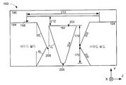
도 4는, 일부 실시형태들에 따라 다양한 구조적 피쳐들로 조정된 자기 엘리먼트(190)의 예의 일 부분의 ABS 관점 블록도를 도시한다. 자기 엘리먼트(190)는, 레터박스(198), 쉴드 측벽들(200 및 202), 및 폴 측벽들(204)과 같은 피쳐들을 변경하는 자기 규모로 각각 구성된, 사이드 쉴드들(194)과 트레일링 쉴드(196) 사이에 배치된 기입 폴(192)을 갖는다. 기입 폴(192)은 선형 트레일링 에지(204) 및 만곡(curved) 리딩 에지 폴 선단(206)으로 구성되고, 이들 사이에 쉴드 선단(208)이 위치결정되어 있으며, 이로부터 쉴드 측벽들(200 및 202)은 각 측벽(200 및 202)이 리딩 에지(206) 및 트레일링 에지(204)의 경계(bound)들을 넘게 되는 길이들로 연장된다.FIG. 4 illustrates an ABS perspective block diagram of a portion of an example of a
도 3의 쉴드 및 폴 측벽들을 가짐으로써, 다양한 측벽들(200, 202 및 204)은 비제한적으로 다양한 각도들(Θ1, Θ2 및 Θ3)로 조정될 수 있으며, 이는 리딩 에지(206), 트레일링 에지(204) 및 쉴드 선단(208)에서 상이한 쉴드 대 폴의 간격들을 허용한다. 다양한 측벽들의 조정된 각도들 및 사이드 쉴드(194)와 기입 폴(192) 사이의 갭의 크기에 관계없이, 기입 폴(192)로부터 다운트랙으로의 레터박스(198)의 포함은, 폴(192)로부터의 자기 플럭스 손실을 최소화하면서 충분한 자기 쉴딩을 제공할 수 있으며, 이는 기입 필드 구배, 진폭, 및 게인(gain)을 증가시킨다. 레터박스(198)는 사이드 쉴드(194) 및 트레일링 쉴드(196)로부터 부분적으로 형성되어 있는 바와 같이 보이지만, 이러한 구성은, 사이드 쉴드(194) 또는 트레일링 쉴드(196) 중 어느 하나의 부분(part)으로서 레터박스를 완전히 통합하도록 기꺼이(at will) 변경될 수 있다.3, the
레터박스(198)의 위치 및 형태는, 기입 폴(192)의 자기 쉴딩과 기입 필드 게인과 구배 사이의 균형을 제공하도록 다양한 실시형태들에서 조정될 수도 있다. 즉, 폭(210)과 기입 폴(198)로부터의 간격(212)은, 기입 폴(192)에 대한 미리결정된 쉴딩 및 자기 성능 특징들을 제공하도록, 연속적인 곡선 및 직사각형과 같은 전체적인 형태에 따라 조정될 수도 있다. 조정된 레터박스(198)의 추가는, 표유 필드들(stray fields)이 기입 폴(192)에 가장 근접한 가장 긴 측벽을 갖는 조정된 쉴드 측벽들(200 및 202)에 의해 제공된 형태 이방성에 의해 적어도 감소됨에 따라, 자기 오버슈트(overshoot)를 감소시킬 수 있다. 레터박스(198)는, 사이드 트랙 삭제를 감소시키고 자기 전이 곡률(magnetic transition curvature)을 증가시키도록, 기입 폴(192)의 리딩 에지(206) 및 트레일링 에지(204) 각각으로부터의 쉴드 선단(208)의 리딩 간격(214) 및 트레일링 간격(216)에 의해 제공된 쉴드 선단(208)의 조정된 위치에 의해 보완될 수도 있다.The position and shape of the
사이드 쉴드들(194), 기입 폴(192) 및 레터박스(198)의 구성들은 쉴딩 재료를, 기입 폴(192)의 선택된 부분들의 미리결정된 근처(proximity)에 위치결정할 수 있으며, 자기적 절연 재료가 쉴드들(194 및 196)과 기입 폴(192) 사이에 배치되는 것을 허용할 수 있는 데 반해, 다양한 자기 엘리먼트(190) 컴포넌트들은 최적화된 자기 기입 필드들을 제공하는 동안 기입 폴(192)의 자기 규모를 조작하도록, 형태, 재료, 크기 및 위치에 대해 더 조정될 수도 있다. 도 5는 다양한 실시형태들에 따라 조정된 자기 엘리먼트(220)의 예의 일 부분의 ABS 관점 블록도를 일반적으로 보여준다. 자기 엘리먼트(220)는, 2개 이상의 쉴드 측벽들을 제공하도록 각각 조정된 사이드 쉴드들(224) 사이에 배치된 기입 폴(222)을 갖는다.The configurations of side shields 194,
도시된 바와 같이, 기입 폴(222)은, 리딩 에지(228) 및 트레일링 에지(230)를 연결하는 반대측으로 대향되는 폴 측벽들(226)을 갖는 실질적으로 사다리꼴의 형태를 갖는다. 각 사이드 쉴드(224)는, 선단 측벽(238)으로 이루어진 쉴드 선단(236)으로부터 미리결정된 각도로 테이퍼진 제 1 쉴드 측벽(232) 및 제 2 쉴드 측벽(234)으로 구성된다. 도 4의 쉴드 선단(208)과 비교하여, 쉴드 선단(236)은 2개의 표면들이 만나는 지점이 아니라, 대신에 다른 쉴드 측벽들(232 및 234)을 연결하는 미리결정된 길이(240)를 갖는 표면이다. 선단 측벽(238)에 대한 선형 표면의 사용은, 또는 대안적으로 일부 실시형태들에서 연속하는 곡선 표면의 사용은, 기입 폴(222)과 사이드 쉴드들(224) 사이의 기입 갭이 폴 측벽(226)에 관해 미리결정된 간격들(242 및 244)로 변화하는 것을 허용하는 또 다른 조정 가능한 구조적 표면을 제공한다.As shown,
선단 측벽(238)의 형태 및 위치는, 쉴드 측벽들(232 및 234)이 일 지점에서 만나는 경우, 쉴드 측벽들이 기입 폴(222)에 지나치게 가까워지게 할 수 있는 각도들로 제 1 쉴드 측벽(232) 및 제 2 쉴드 측벽(234)이 테이퍼지고 연장되는 것을 허용할 수 있다. 예컨대, 선단 측벽(238)의 길이는, 제 2 쉴드 측벽이 기입 폴(222)의 트레일링 에지(230)에 대해 미리결정된 간격을 제공하기 위해, 선단 측벽(238)의 길이(240)가 존재하지 않는 경우보다, 쉴드 선단(236)으로부터 더 작은 각도로 연장되는 것을 허용할 수도 있다. 이러한 더 작은 쉴드 측벽 각도들은 일부 실시형태들에서, 기입 폴(222)로부터 미리결정된 다운트랙 간격(248), 미리결정된 사이드 쉴드 폭(246)을 형성하도록 활용될 수도 있으며, 이는 사이드 쉴드(224) 및/또는 트레일링 쉴드에 레터박스를 추가적으로 제조하지 않고 레터박스 타입의 기입 필드 게인 및 구배 최적화를 생성할 수 있다.The shape and position of the leading
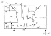
다양한 쉴드 및 폴 측벽들을 조정함으로써 가능한, 광범위하게 다양한 쉴딩 구성들은, 기입 폴(222)의 반대측들 상의 미러 구조들에 제한되는 것은 아니다. 도 6은 일부 실시형태들에 따라 구성된 상이한 사이드 쉴드(264 및 266) 구성들로, 기입 폴(262)의 자기 규모를 제어하도록 자기 엘리먼트(260)의 예가 어떻게 조정될 수 있는지를 일반적으로 도시한다. 자기 엘리먼트(260)의 ABS 관점은, 상이한 자기 쉴딩 특징들 및 구조적 배향들을 갖는 다수의 상이한 재료들의 라미네이션으로서 구성된 제 1 사이드 쉴드(264)를 보여준다.The wide variety of shielding arrangements possible by adjusting the various shield and pole sidewalls are not limited to mirror structures on opposite sides of the
도 6에 도시된 예에서, 제 1 사이드 쉴드(264)는, Y축을 따른 상이한 두께들(274, 276 및 278) 및 폴 측벽(286)(Θ3)에 관한 상이한 각도들(Θ1 및 Θ2)로 배향된 상이한 쉴드 측벽들(280, 282 및 284)을 각각 갖는, 제 1 쉴드 층(268), 제 2 쉴드 층(270), 및 제 3 쉴드 층(272)을 갖는다. 일부 실시형태들은 쉴드 측벽들(280, 282 및 284)들이, 사이드 쉴드(264)와 기입 폴(262)의 리딩 에지 사이에 리딩 간격(288)을 제공하도록 구성하며, 이는 사이드 쉴드(264)와 기입 폴(262)의 트레일링 에지 사이의 트레일링 간격(290)의 절반이다. 트레일링 간격(290)의 절반으로서 리딩 간격(288)을 구성하는 것은, 인접 트랙 간섭을 최소화하도록 최적화된 기입 필드를 제공할 수 있다.6, the
제 1 사이드 쉴드(264)와 기입 폴(262) 사이의 기입 갭을 증가시키는 것은, 상이한 자석 모멘트들을 나타내는 재료들의 사용에 의해 보완될 수 있다. 예컨대, 제 1 층(268)은, 2.4테슬라(Tesla)와 같은 제 1 미리결정된 모멘트로 구성될 수 있는 데 반해, 제 2 층(270)은 1.4테슬라와 같은 상이한 제 2 미리결정된 모멘트를 가지며, 제 3 층(272)은 1.0테슬라와 같은 상이한 제 3 미리결정된 모멘트로 구성된다. 상이한 층들(268, 270 및 272)의 자기 모멘트들을 변화시키는 것은, 특히 리딩 폴 선단(292) 기부에서 표유 자계들이 제어되기 때문에, 기입 필드 손실을 최소화할 수 있다. 기입 폴(262)에 관한 크기, 위치 및 다양한 사이드 쉴드(264) 라미네이션의 재료를 조정하는 능력은, 기입 폴(262)의 정밀한 아티큘레이션(precise articulation)의 자기 특징들과 자기 규모를 허용할 수 있는 추가적인 조정 애스펙트들을 제공한다.Increasing the write gap between the
다수의 상이한 쉴드 층들(268, 270 및 272) 및 재료들의 사용은 정밀한 조정 역량(capability)들을 제공할 수 있는 데 반해, 추가적인 제조의 복잡성 및 프로세싱은 라미네이트된 사이드 쉴드 구성의 효과들을 상쇄시킬 수도 있다. 제 2 사이드 쉴드(266)는, 기입 폴(262)과 제 2 사이드 쉴드(266) 사이에서 가장 근접한 지점인 쉴드 선단(302)을 제작하기 위해, 상이한 각도 배향들(Θ4, Θ5, Θ6 및 Θ7)로 구성된 복수의 쉴드 측벽들(294, 296, 298 및 300)로 단일 층 및 재료가 어떻게 구성될 수 있는지를 보여준다.The use of a number of
쉴드 선단(302)의 위치는, 폴 측벽(286)의 임의의 미리결정된 부분의 기부에 위치결정될 수도 있지만, 이러한 미리결정된 부분은, 사이드 쉴드가 리딩 폴 선단(292)으로부터 다운트랙으로 평면을 연장하는 경우 기입 폴(262)의 트레일링 부분을 더 향할 수도 있다. 즉, 쉴드 선단(302)의 위치는, 사이드 쉴드(266)가 연장되는 다운트랙 간격(304)에 따라 선택될 수도 있다. 이러한 다운트랙 간격(304)은, 미리결정된 인접 트랙 간섭 및 사이드 트랙 삭제 완화를 제공하기 위해 자기 쉴딩과 기입 필드 게인 및 구배의 균형을 이루도록, 리딩 간격(306), 선단 간격(308) 및 트레일링 간격(310)을 더 변경할 수도 있다.The position of the shield tip 302 may be positioned at the base of any predetermined portion of the
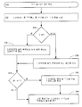
기입 필드 및 데이터 비트 프로그래밍 성능(performance)을 최적화할 수 있는 다양한 비제한적 사이드 쉴드 구성들로, 자기 엘리먼트의 구성은, 자기 동작을 조정하도록 일련의 일반적이며 구체적인 판단들을 받을 수 있다. 도 7은 자기 엘리먼트의 자기 쉴딩 및 자기 기입 필드 성능을 조정하도록, 다양한 실시형태들에 따라 수행된 자기 엘리먼트 제조 루틴(330)의 예를 제공한다. 처음에, 루틴(330)은 단계 332에서, 미리결정된 형태, 측벽들 및 폴 선단으로 기입 폴을 구성한다.With a variety of unrestricted side shield configurations that can optimize write field and data bit programming performance, the configuration of the magnetic element may be subject to a series of general and specific judgments to adjust its magnetic behavior. FIG. 7 provides an example of a magnetic
판단 334는 하나, 또는 양(both) 사이드 쉴드들이 다층 라미네이션으로서 구성되는지의 여부를 판단한다. 복수의 상이한 사이드 쉴드 층들이 판단 334로부터 활용될 경우, 단계 336은 미리결정된 재료들, 두께들 및 쉴드 측벽 각도 배향들로 각 사이드 쉴드 층을 연속적으로 형성한다. 그에 반해, 단계 338은 단일 사이드 쉴드 층을 증착(deposit)하고, 그로부터 연장되는 미리결정된 수의 쉴드 측벽들로 쉴드 선단을 형성한다. 다양한 실시형태들은, 리딩 에지로부터 폴 측벽의 길이의 10%, 30% 또는 50%와 같이 기입 폴의 미리결정된 부분의 기부에 쉴드 선단을 위치결정하는 다른 실시형태들에 따라 쉴드 측벽들이 기입 폴의 리딩 및 트레일링 에지들을 넘어 연장되도록 구성한다.
기입 폴의 반대측들 상에 사이드 쉴드들의 형성은, 단계들 336 및 338을 1회, 또는 다수의 회 수행하는 것을 통해 완수될 수 있음에 주의되어야 한다. 기입 폴의 반대측들 상에 사이드 쉴드들의 형성은, 루틴(330)을 판단 340으로 진전시키며, 여기서 도 4의 레터박스(198)와 같은 레터박스의 포함이 고려된다. 단계 342는, 직사각형, 사다리꼴 및 직사각형 형태들과 같은 미리결정된 형태, 미리결정된 크기 및 기입 폴로부터의 미리결정된 간격을 갖는 레터박스를 형성한다. 이러한 레터박스 구성은, 사이드 쉴드들과, 단계 344에서 후속하여 증착되는 트레일링 쉴드 중 하나 또는 모두(both)의 프로세싱을 통합할 수도 있다. 즉, 레터박스는 사이드 또는 트레일링 쉴드들에 완전히 통합되거나, 사이드 및 트레일링 쉴드들 모두(both)에 의해 제공된 표면들의 조합으로 이루어질 수도 있다.It should be noted that the formation of side shields on opposite sides of the write pole can be accomplished by performing
판단 340에서, 레터박스가 자기 엘리먼트에 통합되지 않는 경우, 단계 344는, 내부의 레터박스 개구를 형성하지 않고 기입 폴로부터 미리결정된 간격으로 트레일링 쉴드를 증착한다. 루틴(330)의 다양한 판단들 및 단계들을 통해, 자기 엘리먼트는, 다양한 사이드 쉴드 측벽들, 간격들 및 쉴드 선단 위치들의 조정된 구성들을 통해 자기 쉴딩과 기입 필드 성능의 균형을 이룸으로써 성능에 대해 최적화될 수 있다. 예컨대, 테이퍼진 쉴드 측벽들 및 쉴드 선단의 위치는, 사이드 트랙 삭제 및 인접 트랙 간섭과 같은 의도하지 않은 성능 특징들의 감소, 또는 최소화된 리스크와 결합되어 더 많은, 또는 더 적은 자기 쉴딩을 제공하도록 기입 폴에 관해 다양한 위치들에 구성될 수 있다.At
그러나, 다양한 판단들 및 단계들이 생략, 변경, 및 추가될 수 있으므로, 도 7에 나타낸 루틴(330)의 다양한 단계들 및 판단들이 요구되거나 제한되는 것은 아님에 주의되어야 한다. 예로서, 판단 334 및 단계들 336 및 338은, 기입 폴의 반대측들 상에 위치결정된 사이드 쉴드들을 구성하도록, 유사하거나 상이한 결과들로 다수의 회들 수행될 수 있다.It should be noted, however, that the various steps and judgments of routine 330 shown in FIG. 7 are not required or limiting, since various judgments and steps may be omitted, changed, and added. By way of example,
미리결정된 자기 쉴딩 및 데이터 비트 프로그래밍 성능을 제공하도록 조정될 수 있는 다양한(plethora) 사이드 쉴드의 구조적 파라미터들은, 기입 폴의 자기 규모를 제어할 수 있는 방대한(vast) 가능성 있는 사이드 쉴드 구성들을 나타낸다. 이러한 사이드 쉴드 구성들은, 최적화된 기입 필드 게인 및 구배를 갖는 강화된 자기장 성능을 제공하도록 조정될 수도 있는 데 반해, 다른 구성들은 잘못된 자기장들 및 사이드 쉴드들의 자기 포화에 기인하는 의도하지 않은 성능 조건들을 최소화하도록 조정될 수도 있다. 기입 폴에 관한 사이드 쉴드들의 다양한 구조적 애스펙트들을 조정함으로써 이들 다양한 성능 특징들의 균형을 이루는 능력은, 특히 증가된 데이터 비트 밀도의, 감소된 형상 계수 데이터 저장 디바이스들에 대한 순응성(adapting)에 관해, 사이드 쉴드 구성의 다용성(versatility)을 나타낸다(convey).The plethora side shield's structural parameters that can be adjusted to provide predetermined magnetic shielding and data bit programming performance represent vast possible side shield configurations that can control the magnetic scale of the write pole. These side shield configurations may be adjusted to provide enhanced magnetic field performance with optimized write field gain and gradient while other configurations minimize unintended performance conditions due to erroneous magnetic fields and magnetic saturation of the side shields . The ability to balance these various performance features by adjusting the various structural aspects of the side shields with respect to the write pole is particularly advantageous in terms of adaptation to reduced shape coefficient data storage devices of increased data bit density, It indicates the versatility of the shield configuration.
게다가, 실시형태들은 자기 프로그래밍에 관한 것인 데 반해, 청구된 발명은 데이터 저장 디바이스 애플리케이션들을 포함하는 임의의 수의 다른 애플리케이션들에서 용이하게 활용될 수 있음이 인식될 것이다. 본 개시물의 다양한 실시형태들의 다수의 특징들 및 구성들이, 다양한 실시형태들의 구조 및 기능의 상세들과 함께 상술한 설명에서 진술되었지만, 본 상세한 설명은 오직 예시이며, 특히 본 개시물의 원리들 내에서, 첨부된 청구항들이 표현되는 용어들의 넓은 일반적인 의미에 의해 명시되는 최대한의 범위(extent)로, 부분들의 구조 및 어레인지먼트들(arrangements)에 관해서 변경들이 구체적으로(in detail) 이루어질 수도 있음이 이해될 것이다. 예컨대, 특정 엘리먼트들은 본 기술의 정신 및 범위(scope)로부터 벗어나지 않고 특정 애플리케이션에 따라 변화할 수도 있다.In addition, it will be appreciated that the embodiments are self-programming whereas the claimed invention can be readily utilized in any number of other applications including data storage device applications. While a number of features and configurations of various embodiments of the disclosure have been set forth in the foregoing description, along with the details of the structure and function of the various embodiments, this description is exemplary only, and in particular, It is to be understood that changes may be made in detail with regard to the structure and arrangements of parts, with the full extent indicated by the broad general meaning of the terms in which the appended claims are expressed . For example, certain elements may vary depending upon the particular application without departing from the spirit and scope of the present technology.
Claims (20)
상기 기입 폴은, 쉴드 선단(shield tip)으로 테이퍼진 제 1 및 제 2 쉴드 측벽들로 구성된 사이드 쉴드 근처이며, 상기 쉴드 선단은 상기 기입 폴과 사이드 쉴드 사이의 가장 근접한 지점인, 장치.An apparatus comprising a write pole having a pole side wall having a successive first taper angle connecting leading and trailing edges,
Wherein the write pole is near a side shield comprising first and second shield side walls tapered to a shield tip and wherein the shield tip is the closest point between the write pole and the side shield.
상기 쉴드 선단은 리딩 및 트레일링 에지들 사이에 위치결정되어 있는, 장치.The method according to claim 1,
Wherein the shield tip is positioned between the leading and trailing edges.
상기 제 1 및 제 2 쉴드 측벽들은, 대각(opposing angles)으로 상기 쉴드 선단으로부터 연장되는, 장치.The method according to claim 1,
Wherein the first and second shield sidewalls extend from the shield tip in opposing angles.
상기 제 1 및 제 2 쉴드 측벽들 중 적어도 하나는, 상기 기입 폴의 상기 리딩 및 트레일링 에지들을 넘어 연속하여 연장되는, 장치.The method according to claim 1,
Wherein at least one of the first and second shield sidewalls extends continuously beyond the leading and trailing edges of the write pole.
상기 제 1 및 제 2 쉴드 측벽들은 상이한 제 2 및 제 3 테이퍼 각도들로 상기 쉴드 선단으로부터 연장되는, 장치.The method according to claim 1,
Wherein the first and second shield sidewalls extend from the shield tip at different second and third taper angles.
상기 쉴드 선단은 상기 리딩 에지의 기부(proximal)에 위치결정되어 있는, 장치.The method according to claim 1,
Wherein the shield tip is positioned at a proximal of the leading edge.
상기 쉴드 선단은, 상기 제 1 및 제 2 쉴드 측벽들을 연결하는 미리결정된 길이를 갖는 선형 측벽을 포함하는, 장치.The method according to claim 1,
Wherein the shield tip comprises a linear sidewall having a predetermined length connecting the first and second shield sidewalls.
상기 선형 측벽은 상기 기입 폴의 상기 트레일링 에지에 직각으로 배향되어 있는, 장치.8. The method of claim 7,
Wherein the linear sidewalls are oriented at right angles to the trailing edge of the write pole.
상기 선형 측벽은 상기 리딩 및 트레일링 에지들 사이에 완전히 위치결정되어 있는, 장치. 8. The method of claim 7,
Wherein the linear side wall is fully positioned between the leading and trailing edges.
상기 쉴드 선단은 상기 리딩 에지로부터 제 1 간격으로 그리고 상기 트레일링 에지로부터 제 2 간격으로 위치결정되어 있으며, 상기 제 1 간격은 상기 트레일링 에지보다 더 작은, 장치.The method according to claim 1,
Wherein the shield tip is positioned at a first distance from the leading edge and at a second distance from the trailing edge, the first distance being less than the trailing edge.
상기 기입 폴은, 쉴드 선단으로 테이퍼진 제 1 및 제 2 쉴드 측벽들로 각각 구성된, 제 1 및 제 2 사이드 쉴드들 사이에 배치되고, 상기 제 1 및 제 2 사이드 쉴드들로부터 분리되며, 상기 쉴드 선단은 상기 기입 폴과 사이드 쉴드 사이의 가장 근접한 지점인, 자기 엘리먼트.1. A magnetic element comprising a write pole having a pole side wall having a successive first taper angle connecting leading and trailing edges,
Wherein the write pole is disposed between first and second side shields, each of which is composed of first and second shield side walls tapered to a shield tip, and is separated from the first and second side shields, And the tip is the closest point between the write pole and the side shield.
상기 제 1 및 제 2 사이드 쉴드들은 상이한 총 수의 쉴드 측벽들을 갖는, 자기 엘리먼트.12. The method of claim 11,
Wherein the first and second side shields have a different total number of shield side walls.
상기 사이드 쉴드들 중 적어도 하나는, 상이한 자기 모멘트들을 갖는 다수의 층들을 포함하는, 자기 엘리먼트.12. The method of claim 11,
Wherein at least one of the side shields comprises a plurality of layers having different magnetic moments.
상기 다수의 층들은 상이한 두께들을 갖는, 자기 엘리먼트.14. The method of claim 13,
The plurality of layers having different thicknesses.
상기 다수의 층들 중 제 1 층은 제 1 자기 모멘트를 갖고 상기 리딩 에지의 기부에 위치결정되어 있으며, 상기 제 1 자기 모멘트는 상기 다수의 층들 중 제 2 층의 제 2 자기 모멘트보다 더 큰, 자기 엘리먼트.14. The method of claim 13,
Wherein a first one of the plurality of layers has a first magnetic moment and is positioned at a base of the leading edge and the first magnetic moment is greater than a second magnetic moment of the second one of the plurality of layers, Element.
레터박스(letterbox)를 형성하도록, 제 1 및 제 2 사이드 쉴드들 모두(both)의 제 1 쉴드 측벽은 상기 트레일링 에지를 넘어 연장되는, 자기 엘리먼트.12. The method of claim 11,
The first shield side wall of both of the first and second side shields extending beyond the trailing edge to form a letterbox.
상기 제 1 및 제 2 사이드 쉴드들 중 적어도 하나의 제 2 쉴드 측벽은 상기 리딩 에지로부터 다운트랙(downtrack)으로 평면을 연장하는, 자기 엘리먼트.12. The method of claim 11,
And a second shield side wall of at least one of the first and second side shields extends in a plane from the leading edge to a down track.
상기 기입 폴은, 쉴드 선단으로 테이퍼진 제 1 및 제 2 쉴드 측벽들로 각각 구성되며 상기 트레일링 에지의 기부에 레터박스를 제공하는 제 1 및 제 2 사이드 쉴드들 사이에 배치되고, 상기 제 1 및 제 2 사이드 쉴드들로부터 분리되며, 상기 쉴드 선단은 상기 기입 폴과 사이드 쉴드 사이의 가장 근접한 지점인, 데이터 라이터.A data writer comprising a write pole having a pole side wall having a successive first taper angle connecting leading and trailing edges,
Wherein the write pole is disposed between first and second side shields each comprising first and second shield side walls tapered to a shield tip and providing a letter box at a base of the trailing edge, And the second side shields, wherein the shield tip is the closest point between the write pole and the side shield.
상기 레터박스는 상기 기입 폴의 폴 폭보다 더 큰 미리결정된 폭을 갖는, 데이터 라이터.19. The method of claim 18,
The letterbox having a predetermined width greater than a pole width of the write pole.
상기 레터박스는 적어도 하나의 사이드 쉴드와 트레일링 쉴드의 결합(union)으로 형성되어 있는, 데이터 라이터.19. The method of claim 18,
Wherein the letter box is formed by a union of at least one side shield and a trailing shield.
Applications Claiming Priority (2)
| Application Number | Priority Date | Filing Date | Title |
|---|---|---|---|
| US13/689,409 US9034150B2 (en) | 2012-11-29 | 2012-11-29 | Thin film with tuned anisotropy and magnetic moment |
| US13/689,409 | 2012-11-29 |
Related Child Applications (1)
| Application Number | Title | Priority Date | Filing Date |
|---|---|---|---|
| KR20150028228A Division KR20150035892A (en) | 2012-11-29 | 2015-02-27 | Data writer with tapered side shield sidewalls |
Publications (1)
| Publication Number | Publication Date |
|---|---|
| KR20140070399A true KR20140070399A (en) | 2014-06-10 |
Family
ID=49916807
Family Applications (2)
| Application Number | Title | Priority Date | Filing Date |
|---|---|---|---|
| KR1020130143035A KR20140070399A (en) | 2012-11-29 | 2013-11-22 | Data writer with tapered side shield sidewalls |
| KR20150028228A KR20150035892A (en) | 2012-11-29 | 2015-02-27 | Data writer with tapered side shield sidewalls |
Family Applications After (1)
| Application Number | Title | Priority Date | Filing Date |
|---|---|---|---|
| KR20150028228A KR20150035892A (en) | 2012-11-29 | 2015-02-27 | Data writer with tapered side shield sidewalls |
Country Status (5)
| Country | Link |
|---|---|
| US (1) | US9034150B2 (en) |
| EP (1) | EP2738137A1 (en) |
| JP (1) | JP6046597B2 (en) |
| KR (2) | KR20140070399A (en) |
| CN (1) | CN103855298B (en) |
Families Citing this family (3)
| Publication number | Priority date | Publication date | Assignee | Title |
|---|---|---|---|---|
| US9856557B1 (en) | 2016-01-22 | 2018-01-02 | Seagate Technology Llc | Fabrication of a multi-layered magnetic element |
| US10170691B2 (en) * | 2016-01-28 | 2019-01-01 | SK Hynix Inc. | Electronic device and method for fabricating the same |
| US11031032B1 (en) * | 2017-04-03 | 2021-06-08 | Seagate Technology Llc | Cryogenic magnetic alloys with less grain refinement dopants |
Family Cites Families (22)
| Publication number | Priority date | Publication date | Assignee | Title |
|---|---|---|---|---|
| JPS62238614A (en) * | 1986-04-09 | 1987-10-19 | Fujitsu Ltd | Manufacture of anistropic magnetic film |
| US5590389A (en) | 1994-12-23 | 1996-12-31 | Johnson Matthey Electronics, Inc. | Sputtering target with ultra-fine, oriented grains and method of making same |
| US5764567A (en) | 1996-11-27 | 1998-06-09 | International Business Machines Corporation | Magnetic tunnel junction device with nonferromagnetic interface layer for improved magnetic field response |
| JP2924785B2 (en) | 1996-04-25 | 1999-07-26 | 日本電気株式会社 | Magnetoresistive element thin film and method of manufacturing the same |
| US6139951A (en) | 1997-12-12 | 2000-10-31 | Seagate Technology Llc | Magnetic recording medium with low temperature seedlayer for high signal-to-noise ratio |
| JP3677423B2 (en) | 1999-12-28 | 2005-08-03 | 株式会社東芝 | Thermally assisted magnetic recording method and thermally assisted magnetic recording apparatus |
| US6740397B1 (en) | 2000-05-24 | 2004-05-25 | Seagate Technology Llc | Subseedlayers for magnetic recording media |
| US6946039B1 (en) | 2000-11-02 | 2005-09-20 | Honeywell International Inc. | Physical vapor deposition targets, and methods of fabricating metallic materials |
| JP3619769B2 (en) * | 2000-11-09 | 2005-02-16 | Tdk株式会社 | Method for manufacturing magnetoresistive element |
| JP3890893B2 (en) * | 2000-12-28 | 2007-03-07 | 日本電気株式会社 | Spin tunnel magnetoresistive film and element, magnetoresistive sensor using the same, magnetic device, and manufacturing method thereof |
| JP2003198002A (en) * | 2001-12-25 | 2003-07-11 | Fujitsu Ltd | Magnetoresistive effect film and ferromagnetic laminated structure |
| US6791796B2 (en) | 2002-05-28 | 2004-09-14 | Seagate Technology Llc | Perpendicular writer with laminated main pole |
| JP2004326888A (en) * | 2003-04-23 | 2004-11-18 | Sony Corp | Magnetic recording medium |
| US6818961B1 (en) * | 2003-06-30 | 2004-11-16 | Freescale Semiconductor, Inc. | Oblique deposition to induce magnetic anisotropy for MRAM cells |
| US7061731B2 (en) | 2003-11-17 | 2006-06-13 | Seagate Technology Llc | High magnetic anisotropy hard magnetic bias element |
| JP4529081B2 (en) * | 2004-11-30 | 2010-08-25 | Tdk株式会社 | Magnetic thin film |
| CN101765677B (en) * | 2007-08-29 | 2012-01-25 | 佳能安内华股份有限公司 | Film deposition method and device by sputtering |
| US7914916B2 (en) | 2008-02-04 | 2011-03-29 | Seagate Technology Llc | Thermally stable high anisotropic high magnetic moment films |
| JPWO2009154009A1 (en) * | 2008-06-20 | 2011-11-24 | キヤノンアネルバ株式会社 | Magnetoresistive element manufacturing method, sputter film forming chamber, magnetoresistive element manufacturing apparatus having sputter film forming chamber, program, and storage medium |
| US8776542B2 (en) * | 2009-12-25 | 2014-07-15 | Canon Anelva Corporation | Cooling system |
| JP2012140672A (en) * | 2010-12-28 | 2012-07-26 | Canon Anelva Corp | Sputtering apparatus |
| JP5882934B2 (en) * | 2012-05-09 | 2016-03-09 | シーゲイト テクノロジー エルエルシー | Sputtering equipment |
-
2012
- 2012-11-29 US US13/689,409 patent/US9034150B2/en active Active
-
2013
- 2013-11-22 KR KR1020130143035A patent/KR20140070399A/en not_active Application Discontinuation
- 2013-11-27 EP EP20130194711 patent/EP2738137A1/en not_active Ceased
- 2013-11-28 JP JP2013246158A patent/JP6046597B2/en not_active Expired - Fee Related
- 2013-11-28 CN CN201310625298.0A patent/CN103855298B/en active Active
-
2015
- 2015-02-27 KR KR20150028228A patent/KR20150035892A/en not_active Application Discontinuation
Also Published As
| Publication number | Publication date |
|---|---|
| CN103855298A (en) | 2014-06-11 |
| JP6046597B2 (en) | 2016-12-21 |
| US20140147702A1 (en) | 2014-05-29 |
| US9034150B2 (en) | 2015-05-19 |
| CN103855298B (en) | 2017-12-22 |
| JP2014112677A (en) | 2014-06-19 |
| KR20150035892A (en) | 2015-04-07 |
| EP2738137A1 (en) | 2014-06-04 |
Similar Documents
| Publication | Publication Date | Title |
|---|---|---|
| US9218824B2 (en) | Data writer with tapered side shield sidewalls | |
| US8922950B2 (en) | Multi-layer magnetoresistive shield with transition metal layer | |
| US8830626B2 (en) | Write pole with shaped box shield | |
| JP6050266B2 (en) | Device with write pole, magnetic element, and data writer | |
| US8472147B2 (en) | Magnetoresistive shield with lateral sub-magnets | |
| JP5829651B2 (en) | Apparatus, magnetic element, and conversion head | |
| JP6038842B2 (en) | Data writing device with magnetic flux density insert | |
| US8842396B1 (en) | Magnetic sensor with differing stripe heights | |
| US20120281314A1 (en) | Magnetic Shield with Flux Concentration Feature | |
| US8885300B2 (en) | Magnetic element with a bi-layer side shield | |
| US20150103439A1 (en) | Write pole with varying bevel angles | |
| KR101609730B1 (en) | Side shield with variable anisotropy | |
| KR20150035892A (en) | Data writer with tapered side shield sidewalls | |
| US9697852B2 (en) | Single coil turn data writer | |
| JP5992972B2 (en) | Data reader having horizontal laminated shield and method for manufacturing the same | |
| US9099108B2 (en) | Magnetically biased write pole | |
| US20140300995A1 (en) | Data Writer with Yoke Shaped Write Pole | |
| US9728207B2 (en) | Write pole magnetic guard | |
| KR20130112000A (en) | Write yoke with stabilizing layer |
Legal Events
| Date | Code | Title | Description |
|---|---|---|---|
| A201 | Request for examination | ||
| E902 | Notification of reason for refusal | ||
| A107 | Divisional application of patent | ||
| E601 | Decision to refuse application | ||
| WITB | Written withdrawal of application |