KR20140063790A - Compositions of neutral layer for directed self assembly block copolymers and processes thereof - Google Patents
Compositions of neutral layer for directed self assembly block copolymers and processes thereof Download PDFInfo
- Publication number
- KR20140063790A KR20140063790A KR1020147009536A KR20147009536A KR20140063790A KR 20140063790 A KR20140063790 A KR 20140063790A KR 1020147009536 A KR1020147009536 A KR 1020147009536A KR 20147009536 A KR20147009536 A KR 20147009536A KR 20140063790 A KR20140063790 A KR 20140063790A
- Authority
- KR
- South Korea
- Prior art keywords
- neutral layer
- photoresist
- block
- pattern
- block copolymer
- Prior art date
Links
Images


Classifications
-
- G—PHYSICS
- G03—PHOTOGRAPHY; CINEMATOGRAPHY; ANALOGOUS TECHNIQUES USING WAVES OTHER THAN OPTICAL WAVES; ELECTROGRAPHY; HOLOGRAPHY
- G03F—PHOTOMECHANICAL PRODUCTION OF TEXTURED OR PATTERNED SURFACES, e.g. FOR PRINTING, FOR PROCESSING OF SEMICONDUCTOR DEVICES; MATERIALS THEREFOR; ORIGINALS THEREFOR; APPARATUS SPECIALLY ADAPTED THEREFOR
- G03F7/00—Photomechanical, e.g. photolithographic, production of textured or patterned surfaces, e.g. printing surfaces; Materials therefor, e.g. comprising photoresists; Apparatus specially adapted therefor
- G03F7/20—Exposure; Apparatus therefor
-
- C—CHEMISTRY; METALLURGY
- C08—ORGANIC MACROMOLECULAR COMPOUNDS; THEIR PREPARATION OR CHEMICAL WORKING-UP; COMPOSITIONS BASED THEREON
- C08L—COMPOSITIONS OF MACROMOLECULAR COMPOUNDS
- C08L53/00—Compositions of block copolymers containing at least one sequence of a polymer obtained by reactions only involving carbon-to-carbon unsaturated bonds; Compositions of derivatives of such polymers
-
- B—PERFORMING OPERATIONS; TRANSPORTING
- B82—NANOTECHNOLOGY
- B82Y—SPECIFIC USES OR APPLICATIONS OF NANOSTRUCTURES; MEASUREMENT OR ANALYSIS OF NANOSTRUCTURES; MANUFACTURE OR TREATMENT OF NANOSTRUCTURES
- B82Y10/00—Nanotechnology for information processing, storage or transmission, e.g. quantum computing or single electron logic
-
- B—PERFORMING OPERATIONS; TRANSPORTING
- B82—NANOTECHNOLOGY
- B82Y—SPECIFIC USES OR APPLICATIONS OF NANOSTRUCTURES; MEASUREMENT OR ANALYSIS OF NANOSTRUCTURES; MANUFACTURE OR TREATMENT OF NANOSTRUCTURES
- B82Y40/00—Manufacture or treatment of nanostructures
-
- C—CHEMISTRY; METALLURGY
- C08—ORGANIC MACROMOLECULAR COMPOUNDS; THEIR PREPARATION OR CHEMICAL WORKING-UP; COMPOSITIONS BASED THEREON
- C08F—MACROMOLECULAR COMPOUNDS OBTAINED BY REACTIONS ONLY INVOLVING CARBON-TO-CARBON UNSATURATED BONDS
- C08F212/00—Copolymers of compounds having one or more unsaturated aliphatic radicals, each having only one carbon-to-carbon double bond, and at least one being terminated by an aromatic carbocyclic ring
- C08F212/02—Monomers containing only one unsaturated aliphatic radical
- C08F212/04—Monomers containing only one unsaturated aliphatic radical containing one ring
- C08F212/06—Hydrocarbons
- C08F212/08—Styrene
-
- C—CHEMISTRY; METALLURGY
- C08—ORGANIC MACROMOLECULAR COMPOUNDS; THEIR PREPARATION OR CHEMICAL WORKING-UP; COMPOSITIONS BASED THEREON
- C08F—MACROMOLECULAR COMPOUNDS OBTAINED BY REACTIONS ONLY INVOLVING CARBON-TO-CARBON UNSATURATED BONDS
- C08F212/00—Copolymers of compounds having one or more unsaturated aliphatic radicals, each having only one carbon-to-carbon double bond, and at least one being terminated by an aromatic carbocyclic ring
- C08F212/02—Monomers containing only one unsaturated aliphatic radical
- C08F212/32—Monomers containing only one unsaturated aliphatic radical containing two or more rings
-
- C—CHEMISTRY; METALLURGY
- C08—ORGANIC MACROMOLECULAR COMPOUNDS; THEIR PREPARATION OR CHEMICAL WORKING-UP; COMPOSITIONS BASED THEREON
- C08F—MACROMOLECULAR COMPOUNDS OBTAINED BY REACTIONS ONLY INVOLVING CARBON-TO-CARBON UNSATURATED BONDS
- C08F220/00—Copolymers of compounds having one or more unsaturated aliphatic radicals, each having only one carbon-to-carbon double bond, and only one being terminated by only one carboxyl radical or a salt, anhydride ester, amide, imide or nitrile thereof
- C08F220/02—Monocarboxylic acids having less than ten carbon atoms; Derivatives thereof
- C08F220/10—Esters
- C08F220/12—Esters of monohydric alcohols or phenols
- C08F220/14—Methyl esters, e.g. methyl (meth)acrylate
-
- C—CHEMISTRY; METALLURGY
- C08—ORGANIC MACROMOLECULAR COMPOUNDS; THEIR PREPARATION OR CHEMICAL WORKING-UP; COMPOSITIONS BASED THEREON
- C08F—MACROMOLECULAR COMPOUNDS OBTAINED BY REACTIONS ONLY INVOLVING CARBON-TO-CARBON UNSATURATED BONDS
- C08F293/00—Macromolecular compounds obtained by polymerisation on to a macromolecule having groups capable of inducing the formation of new polymer chains bound exclusively at one or both ends of the starting macromolecule
-
- C—CHEMISTRY; METALLURGY
- C09—DYES; PAINTS; POLISHES; NATURAL RESINS; ADHESIVES; COMPOSITIONS NOT OTHERWISE PROVIDED FOR; APPLICATIONS OF MATERIALS NOT OTHERWISE PROVIDED FOR
- C09D—COATING COMPOSITIONS, e.g. PAINTS, VARNISHES OR LACQUERS; FILLING PASTES; CHEMICAL PAINT OR INK REMOVERS; INKS; CORRECTING FLUIDS; WOODSTAINS; PASTES OR SOLIDS FOR COLOURING OR PRINTING; USE OF MATERIALS THEREFOR
- C09D125/00—Coating compositions based on homopolymers or copolymers of compounds having one or more unsaturated aliphatic radicals, each having only one carbon-to-carbon double bond, and at least one being terminated by an aromatic carbocyclic ring; Coating compositions based on derivatives of such polymers
- C09D125/02—Homopolymers or copolymers of hydrocarbons
- C09D125/04—Homopolymers or copolymers of styrene
- C09D125/08—Copolymers of styrene
- C09D125/14—Copolymers of styrene with unsaturated esters
-
- C—CHEMISTRY; METALLURGY
- C09—DYES; PAINTS; POLISHES; NATURAL RESINS; ADHESIVES; COMPOSITIONS NOT OTHERWISE PROVIDED FOR; APPLICATIONS OF MATERIALS NOT OTHERWISE PROVIDED FOR
- C09D—COATING COMPOSITIONS, e.g. PAINTS, VARNISHES OR LACQUERS; FILLING PASTES; CHEMICAL PAINT OR INK REMOVERS; INKS; CORRECTING FLUIDS; WOODSTAINS; PASTES OR SOLIDS FOR COLOURING OR PRINTING; USE OF MATERIALS THEREFOR
- C09D125/00—Coating compositions based on homopolymers or copolymers of compounds having one or more unsaturated aliphatic radicals, each having only one carbon-to-carbon double bond, and at least one being terminated by an aromatic carbocyclic ring; Coating compositions based on derivatives of such polymers
- C09D125/02—Homopolymers or copolymers of hydrocarbons
- C09D125/16—Homopolymers or copolymers of alkyl-substituted styrenes
-
- G—PHYSICS
- G03—PHOTOGRAPHY; CINEMATOGRAPHY; ANALOGOUS TECHNIQUES USING WAVES OTHER THAN OPTICAL WAVES; ELECTROGRAPHY; HOLOGRAPHY
- G03F—PHOTOMECHANICAL PRODUCTION OF TEXTURED OR PATTERNED SURFACES, e.g. FOR PRINTING, FOR PROCESSING OF SEMICONDUCTOR DEVICES; MATERIALS THEREFOR; ORIGINALS THEREFOR; APPARATUS SPECIALLY ADAPTED THEREFOR
- G03F7/00—Photomechanical, e.g. photolithographic, production of textured or patterned surfaces, e.g. printing surfaces; Materials therefor, e.g. comprising photoresists; Apparatus specially adapted therefor
- G03F7/0002—Lithographic processes using patterning methods other than those involving the exposure to radiation, e.g. by stamping
-
- G—PHYSICS
- G03—PHOTOGRAPHY; CINEMATOGRAPHY; ANALOGOUS TECHNIQUES USING WAVES OTHER THAN OPTICAL WAVES; ELECTROGRAPHY; HOLOGRAPHY
- G03F—PHOTOMECHANICAL PRODUCTION OF TEXTURED OR PATTERNED SURFACES, e.g. FOR PRINTING, FOR PROCESSING OF SEMICONDUCTOR DEVICES; MATERIALS THEREFOR; ORIGINALS THEREFOR; APPARATUS SPECIALLY ADAPTED THEREFOR
- G03F7/00—Photomechanical, e.g. photolithographic, production of textured or patterned surfaces, e.g. printing surfaces; Materials therefor, e.g. comprising photoresists; Apparatus specially adapted therefor
- G03F7/20—Exposure; Apparatus therefor
- G03F7/2037—Exposure with X-ray radiation or corpuscular radiation, through a mask with a pattern opaque to that radiation
Landscapes
- Chemical & Material Sciences (AREA)
- Engineering & Computer Science (AREA)
- Organic Chemistry (AREA)
- Health & Medical Sciences (AREA)
- Chemical Kinetics & Catalysis (AREA)
- Medicinal Chemistry (AREA)
- Polymers & Plastics (AREA)
- Physics & Mathematics (AREA)
- Nanotechnology (AREA)
- General Physics & Mathematics (AREA)
- Crystallography & Structural Chemistry (AREA)
- Life Sciences & Earth Sciences (AREA)
- Materials Engineering (AREA)
- Wood Science & Technology (AREA)
- Theoretical Computer Science (AREA)
- Condensed Matter Physics & Semiconductors (AREA)
- Mathematical Physics (AREA)
- Manufacturing & Machinery (AREA)
- Graft Or Block Polymers (AREA)
- Exposure Of Semiconductors, Excluding Electron Or Ion Beam Exposure (AREA)
- Photosensitive Polymer And Photoresist Processing (AREA)
- Materials For Photolithography (AREA)
- Compositions Of Macromolecular Compounds (AREA)
Abstract
본 발명은 신규의 중성층 조성물 및 유도 자기조립 블록 공중합체(BCP)의 마이크로도메인의 정렬을 위한 중성층 조성물의 사용 방법에 관한 것이다. 조성물 및 방법은 전자 소자의 제작에 유용하다. 중성층 조성물은 하나 이상의 구조 단위 (1), 하나 이상의 구조 단위 (2) 및 하나 이상의 구조 단위 (3)을 가진 하나 이상의 랜덤 공중합체를 포함하고,

여기서 R1은 C1-C8 알킬, C1-C8 플루오로알킬 모이어티, C1-C8 부분적으로 플루오르화된 알킬, C4-C8 사이클로알킬, C4-C8 사이클로플루오로알킬, C4-C8 부분적으로 플루오르화된 사이클로알킬, 및 C2-C8 히드록시알킬로 구성된 군으로부터 선택되고; R2, R3 및 R5는 H, C1-C4 알킬, CF3 및 F로 구성된 군으로부터 독립적으로 선택되고; R4는 H, C1-C8 알킬, C1-C8 부분적으로 플루오르화된 알킬 및 C1-C8 플루오로알킬로 구성된 군으로부터 선택되고, n은 1 내지 5 범위이고, R6은 H, F, C1-C8 알킬 및 C1-C8 플루오로알킬로 구성된 군으로부터 선택되고 m은 1 내지 3 범위이다.The present invention relates to a novel neutral layer composition and a method of using the neutral layer composition for the alignment of the microdomains of an induced self-assembled block copolymer (BCP). The compositions and methods are useful for making electronic devices. The neutral layer composition comprises at least one random copolymer having at least one structural unit (1), at least one structural unit (2) and at least one structural unit (3)
Wherein R 1 is selected from the group consisting of C 1 -C 8 alkyl, C 1 -C 8 fluoroalkyl moiety, C 1 -C 8 partially fluorinated alkyl, C 4 -C 8 cycloalkyl, C 4 -C 8 cyclofluoro Alkyl, C 4 -C 8 partially fluorinated cycloalkyl, and C 2 -C 8 hydroxyalkyl; R 2, R 3 and R 5 are independently selected from the group consisting of H, C 1 -C 4 alkyl, CF 3 and F; R 4 is selected from the group consisting of H, C 1 -C 8 alkyl, C 1 -C 8 partially fluorinated alkyl and C 1 -C 8 fluoroalkyl, n ranges from 1 to 5, and R 6 is Is selected from the group consisting of H, F, C 1 -C 8 alkyl and C 1 -C 8 fluoroalkyl, and m ranges from 1 to 3.
Description
본 발명은 신규의 중성층 조성물 및 유도 자기조립 블록 공중합체(BCP)의 마이크로도메인의 정렬을 위한 중성층 조성물의 신규의 사용 방법에 관한 것이다. 조성물 및 방법은 전자 소자의 제작에 유용하다.The present invention relates to a novel method of using a neutral layer composition and a neutral layer composition for the alignment of microdomains of an induced self-assembled block copolymer (BCP). The compositions and methods are useful for making electronic devices.
블록 공중합체의 유도 자기조립(directed self assembly)은, 나노규모 크기의 특징부의 임계 치수(CD)가 달성될 수 있는 미세전자 소자의 제조를 위한 보다 작은 패턴화된 특징부를 제조하기 위해 유용한 방법이다. 유도 자기조립 방법은 마이크로리소그래피 기술의 해상 능력을 확장하기 위해 바람직하다. 통상적인 리소그래피 접근법에서는, 자외선(UV) 방사선이 기판 또는 층상(layered) 기판 상에 코팅된 포토레지스트층 상에 마스크를 통한 노광을 실시하는데 사용될 수 있다. 포지티브 또는 네거티브 포토레지스트가 유용하며 이들은 또한 통상적인 집적 회로(IC) 플라즈마 처리를 이용한 건식 현상을 가능하게 하기 위해 규소와 같은 내화성 원소를 함유할 수 있다. 포지티브 포토레지스트에서, 마스크를 통해 투과된 UV 방사선은, 노광 영역이 현상액으로 제거되거나 통상적인 IC 플라즈마 처리에 의해 제거되도록 포토레지스트에서 광화학 반응을 야기한다. 반면에, 네거티브 포토레지스트에서는, 마스크를 통해 투과된 UV 방사선이, 방사선에 노출된 영역을 현상액 또는 통상적인 IC 플라즈마 처리에 의해 덜 제거가능하게 한다. 집적 회로 특징부, 예컨대 게이트, 비아(via) 또는 도선(interconnect)이 이후 기판 또는 층상 기판에 에칭되고, 남은 포토레지스트가 제거된다. 통상적인 리소그래피 노광 공정을 사용하면, 집적 회로 특징부의 특징부 치수가 제약된다. 변형(aberrations), 초점(focus), 근위(proximity) 효과, 최소 달성가능한 노광 파장 및 최대 달성가능한 개구수(numerical apertures)와 관련된 한계로 인해 방사선 노광을 사용하여 패턴 치수에 있어 추가 감소는 달성하기가 어렵다. 대규모 집적에 대한 요구는 소자에 있어 회로 치수 및 특징부의 계속된 축소를 야기하고 있다. 과거에는, 특징부의 최종 해상도는 그 자체로 한계를 가지고 있는 포토레지스트 노광에 사용된 광 파장에 의존해 왔다. 직접 조립 기법, 예컨대 블록 공중합체 이미징을 이용한 그라포에피택시(graphoepitaxy) 및 케모에피택시(chemoepitaxy)가 CD 편차를 감소시키면서 해상도를 증가시키기 위해 사용되는 매우 바람직한 기법이다. 이들 기법은 통상적인 UV 리소그래피 기법을 향상시키는데 사용되거나 또는 EUV, e-빔, 원자외선(deep UV) 또는 액침(immersion) 리소그래피를 사용하는 접근법에서 보다 높은 해상도 및 CD 제어를 가능하게 하는데 사용될 수 있다. 유도 자기조립 블록 공중합체는 내에칭성 공중합체 단위의 블록 및 고에칭성 공중합체 단위의 블록을 포함하고, 이는 기판 상에 코팅, 정렬 및 에칭될 경우 초고밀도 패턴 영역을 제공한다.Directed self assembly of block copolymers is a useful method for producing smaller patterned features for the fabrication of microelectronic devices where the critical dimension (CD) of nanoscale sized features can be achieved . Inductive self-assembly methods are desirable to extend the resolution capabilities of microlithography techniques. In a typical lithographic approach, ultraviolet (UV) radiation can be used to effect exposure through a mask on a substrate or a layer of photoresist coated on a layered substrate. Positive or negative photoresists are useful and they may also contain refractory elements such as silicon to enable dry development using conventional integrated circuit (IC) plasma processing. In a positive photoresist, UV radiation transmitted through the mask causes a photochemical reaction in the photoresist such that the exposed areas are removed by a developer or removed by conventional IC plasma treatment. On the other hand, in a negative photoresist, the UV radiation transmitted through the mask makes the region exposed to the radiation less susceptible to removal by developer or conventional IC plasma treatment. Integrated circuit features such as gates, vias, or interconnects are then etched into the substrate or layered substrate and the remaining photoresist is removed. Using a conventional lithographic exposure process, the feature dimensions of the integrated circuit features are constrained. Additional reductions in pattern dimensions using radiation exposure due to limitations associated with aberrations, focus, proximity effects, minimum attainable exposure wavelengths, and numerical apertures are achievable Is difficult. The demand for large scale integration has resulted in continued shrinking of circuit dimensions and features in the device. In the past, the final resolution of features has depended on the light wavelength used in photoresist exposure, which has its limitations. Direct assembly techniques, such as graphoepitaxy and chemoepitaxy using block copolymer imaging, are highly desirable techniques used to increase resolution while reducing CD bias. These techniques can be used to enhance conventional UV lithography techniques or to enable higher resolution and CD control in approaches using EUV, e-beam, deep UV or immersion lithography . Induced self-assembled block copolymers include blocks of etch resistant copolymer units and blocks of high etchable copolymer units, which provide an ultra-high density pattern region when coated, aligned and etched on the substrate.
그라포에피택시 유도 자기조립 방법에서, 블록 공중합체는 통상적인 리소그래피(자외선, 원자외선, e-빔, 극자외선(Extreme UV; EUV) 노광원)로 사전 패턴화된 기판 주위에 자기 조직화(self organize)되어 라인/스페이스(L/S) 또는 컨택홀(CH) 패턴과 같은 반복적인 토포그래픽 특징부를 형성한다. L/S 유도 자기조립 어레이의 일례에서, 블록 공중합체는 사전 패턴화된 라인들 사이의 트렌치에서 상이한 피치의 평행한 라인-스페이스 패턴을 형성할 수 있는 자기-정렬된 라멜라 영역을 형성할 수 있어, 토포그래픽 라인들 간의 트렌치에서 스페이스를 보다 미세한 패턴으로 세분화함으로써 패턴 해상도를 향상시킨다. 예를 들어, 마이크로상 분리가 가능하고, 플라즈마 에칭에 대해 내성인 탄소 풍부 블록(예컨대 스티렌, 또는 Si, Ge, Ti와 같은 몇몇 다른 원소를 함유함) 및 고도로 플라즈마 에칭가능하거나 제거가능한 블록을 포함하는 디블록 공중합체가 고해상도 패턴 형성을 제공할 수 있다. 고에칭성 블록의 예는, 산소가 풍부하고 내화성 원소를 함유하지 않는 단량체를 포함할 수 있고 고에칭성인 블록, 예컨대 메틸메타크릴레이트를 형성할 수 있다. 자기조립 패턴을 규정하는 에칭 공정에 사용되는 플라즈마 에칭 가스는 전형적으로 집적 회로(IC) 제조에 이용된 공정에서 사용되는 가스들이다. 이러한 방식으로, 통상적인 리소그래피 기법에 의해 규정가능한 것보다 매우 미세한 패턴이 전형적인 IC 기판에서 형성될 수 있어, 패턴증배(pattern multiplication)를 달성한다. 마찬가지로, 컨택홀과 같은 특징부는, 적당한 블록 공중합체가 통상적인 리소그래피에 의해 규정된 컨택홀 또는 포스트(posts)의 어레이 주변에 유도 자기조립에 의해 스스로 배열되어지는 그라포에피택시를 사용함으로써 보다 치밀하게 형성되어, 에칭시 컨택홀의 보다 치밀한 어레이를 유도하는 에칭성 및 내에칭성 도메인 영역의 보다 치밀한 어레이를 형성할 수 있다. 결국, 그라포에피택시는 패턴수정(pattern rectification) 및 패턴증배 둘다를 제공하는 잠재력을 가진다. In the grapoeepitaxy induced self-assembly process, the block copolymer is self-assembled (self-assembled) around the pre-patterned substrate with conventional lithography (ultraviolet, deep ultraviolet, e-beam, Extreme UV to form repetitive topographic features such as line / space (L / S) or contact hole (CH) patterns. In one example of an L / S inductively self-assembled array, the block copolymer can form a self-aligned lamella region that can form parallel line-space patterns of different pitches in trenches between pre-patterned lines , The pattern resolution is improved by refining the space in the trench between the topographic lines into a finer pattern. (E. G., Containing some other element such as styrene, or Si, Ge, Ti) and a plasma etchable or removable block that is micro-phase separable and resistant to plasma etching Diblock copolymer can provide high resolution pattern formation. Examples of high etchability blocks may include monomers that are rich in oxygen and do not contain refractory elements and may form high etchable blocks such as methyl methacrylate. Plasma etching gases used in etching processes that define self-assembled patterns are typically the gases used in the process used to fabricate integrated circuits (ICs). In this way, a much finer pattern than can be defined by conventional lithography techniques can be formed in a typical IC substrate, achieving pattern multiplication. Likewise, features such as contact holes can be made more compact by employing grapoe epitaxy where the appropriate block copolymers are self-aligned by induction self-assembly around contact holes or posts arrays defined by conventional lithography To form a more compact array of etchable and etch resistant domain regions that induce a more compact array of contact holes during etching. As a result, graphee epitaxy has the potential to provide both pattern rectification and pattern multiplication.
화학적 에피택시 또는 피닝(pinning) 화학적 에피택시에서 블록 공중합체의 자기조립은, 화학적 친화도가 상이하지만 자기조립 공정을 가이드하는 토포그래피가 없거나 매우 약한 영역을 가진 표면 주위에서 이루어진다. 예를 들어, 기판의 표면이 통상적인 리소그래피(UV, 원자외선, e-빔 EUV)에 의해 패턴화되어 라인 앤 스페이스(L/S) 패턴에서 상이한 화학적 친화도의 표면을 형성할 수 있으며 이 패턴에서는 방사선에 의해 표면 화학이 개질되어진 노출 영역이 노출되지 않고 화학적 변화를 보이지 않는 영역과 교대로 존재한다. 이들 영역은 토포그래픽 차이를 나타내지 않지만, 블록 공중합체 세그먼트의 자기조립을 지시하는 표면 화학적 차이 또는 피닝을 나타낸다. 구체적으로, 블록 세그먼트가 내에칭성의 (예, 스티렌 반복 단위) 및 빠르게 에칭되는 반복 단위(예, 메틸 메타크릴레이트 반복 단위)를 함유하는 블록 공중합체의 유도 자기조립은 패턴 위에 내에칭성 블록 세그먼트 및 고에칭성 블록 세그먼트의 정밀한 배치를 가능하게 한다. 이러한 기법은 이들 블록 공중합체의 정밀한 배치와, 플라즈마 또는 습식 에칭 공정 후 기판으로의 패턴의 후속적인 패턴 전사를 가능하게 한다. 화학적 에피택시는 라인-에지 거칠기 및 CD 제어를 개선하는 것을 돕기 위해 화학적 차이에 있어 변화에 의해 미세 튜닝될 수 있는 이점을 가지고 있으며, 이에 따라 패턴수정이 가능해진다. 다른 타입의 패턴, 예컨대 반복되는 컨택홀(CH) 어레이가 또한 케모에피택시를 사용하여 패턴수정될 수 있다.Self-assembly of block copolymers in chemical epitaxy or pinning chemical epitaxy takes place around a surface that has different chemical affinities but has no or very weak regions to guide the self-assembly process. For example, the surface of the substrate may be patterned by conventional lithography (UV, far ultraviolet, e-beam EUV) to form a surface of a different chemical affinity in a line-and-space (L / S) pattern, , The exposed regions where the surface chemistry was modified by radiation exist in alternation with regions that are not exposed and do not exhibit chemical changes. These regions do not exhibit topographical differences but represent surface chemical differences or pinning indicating self-assembly of the block copolymer segment. Specifically, the induction self-assembly of a block copolymer containing a block segment with an etch-resistant (e.g., styrene repeat unit) and a rapidly etched repeat unit (e.g., a methyl methacrylate repeat unit) And precise placement of the high etch block segments. This technique enables precise placement of these block copolymers and subsequent pattern transfer of the pattern to the substrate after a plasma or wet etch process. Chemical epitaxy has the advantage that it can be finely tuned by changes in chemical differences to help improve line-edge roughness and CD control, thereby allowing pattern modification. Other types of patterns, such as repeating contact hole (CH) arrays, can also be patterned using a chemo-epitaxy.
중성층(중립층)은 유도 자기조립에 이용된 블록 공중합체의 블록 세그먼트에 대해 친화성(affinity)을 가지지 않은 기판 상의 층이거나 처리된 기판의 표면이다. 블록 공중합체의 유도 자기조립의 그라포에피택시 방법에서, 중성층은, 기판에 대해 내에칭성 블록 중합체 세그먼트 및 고에칭성 블록 중합체 세그먼트의 적절한 배치를 유도하는 유도 자기조립을 위해 블록 중합체 세그먼트의 적절한 배치 또는 배향을 허락하기 때문에 유용하다. 예를 들어, 통상적인 방사선 리소그래피에 의해 규정된 라인 앤 스페이스 특징부를 함유한 표면에서, 중성층은 블록 세그먼트가 기판의 표면에 수직으로 배향되도록 블록 세그먼트를 배향시킬 수 있고, 배향은 통상적인 리소그래피에 의해 규정된 라인들 간의 길이와 관련하여 블록 공중합체 중 블록 세그먼트의 길이에 좌우되는 패턴수정 및 배턴증배 둘다의 경우에 이상적이다. 기판이 블록 세그먼트 중 하나와 너무 강하게 상호작용한다면, 세그먼트가 그러한 표면 상에 편평하게 놓이게되어 세그먼트와 기판 간의 접촉 표면을 최대화하며; 이러한 표면은 통상적인 리소그래피를 통해 형성된 특징부에 기초하여 패턴수정 또는 패턴증배를 달성하는데 사용될 수 있는 원하는 수직 정렬을 방해한다. 기판의 선택된 작은 영역 또는 피닝이 블록 공중합체의 일 블록과 강하게 상호작용하도록 하고 표면의 나머지를 중성층으로 코팅되도록 개질하면 블록 공중합체의 도메인이 원하는 방향으로 배열하도록 하는데 유용할 수 있고, 이는 패턴증배를 위해 이용되는 피닝된 케모에피택시 또는 그라포에피택시에 대한 기초가 된다.The neutral layer is a layer on the substrate that does not have affinity for the block segment of the block copolymer used for inductive self-assembly or the surface of the treated substrate. In a grapoeepitaxy method of induction self-assembly of block copolymers, the neutral layer is formed of a block polymer segment for induction self-assembly to induce proper placement of the etchable block polymer segment and the etchable block polymer segment relative to the substrate. This is useful because it permits proper placement or orientation. For example, in a surface containing line and space features defined by conventional radiation lithography, the neutral layer may orient the block segments such that the block segments are oriented perpendicularly to the surface of the substrate, and the orientation may be determined by conventional lithography Which is dependent on the length of the block segment of the block copolymer with respect to the length between the lines defined by the pattern. If the substrate is too strongly interacting with one of the block segments, the segment will lie flat on such surface to maximize the contact surface between the segment and the substrate; This surface hinders the desired vertical alignment that can be used to achieve pattern modification or pattern multiplication based on features formed through conventional lithography. Modifying a selected small region or pinning of the substrate to strongly interact with one block of the block copolymer and coating the remainder of the surface with the neutral layer may be useful to cause the domains of the block copolymer to align in the desired direction, It is the basis for pinned chemo-epitaxy or grape epitaxy used for multiplication.
이에 따라, 층으로 형성될 경우 자기조립 블록 공중합체에 대해 중성(중립) 상태로 남고 유도 자기조립 기법의 공정 단계에 의해 손상되지 않으면서, 나아가 유도 자기조립 재료 및 공정의 리소그래피 성능을 향상시켜, 특히 공정처리 단계의 수를 감소시키고 우수한 리소그래피 성능을 가진 보다 우수한 패턴 해상도를 제공하는 중성층 조성물에 대한 요구가 존재한다. 본 발명은 자기조립 블록 공중합체에 대해 중성인 층을 형성하고 우수한 리소그래피 성능을 가진 패턴을 제공하는 신규의 공정 및 신규의 중성층 조성물에 관한 것이다.Thus, when formed as a layer, it remains neutral to the self-assembled block copolymer and is not damaged by the process steps of inductive self-assembly techniques, further enhancing the lithographic performance of the induced self-assembled material and process, There is a need in particular for a neutral layer composition that reduces the number of process steps and provides better pattern resolution with excellent lithographic performance. The present invention relates to a novel process and a novel neutral layer composition which forms a neutral layer for self-assembled block copolymers and provides a pattern with excellent lithographic performance.
발명의 요약SUMMARY OF THE INVENTION
본 발명은 신규의 중성층 조성물, 및 유도 자기조립 블록 공중합체(BCP)의 마이크로도메인을 정렬하기 위해 중성층 조성물을 사용하는 신규의 방법에 관한 것이다. 중성층 조성물은 하나 이상의 구조 단위 (1), 하나 이상의 구조 단위 (2) 및 하나 이상의 구조 단위 (3)을 가진 하나 이상의 랜덤 공중합체를 포함한다:The present invention relates to a novel neutral layer composition, and a novel method of using a neutral layer composition to align the microdomains of an induced self-assembled block copolymer (BCP). The neutral layer composition comprises at least one random copolymer having at least one structural unit (1), at least one structural unit (2) and at least one structural unit (3)

상기 식에서 R1은 C1-C8 알킬, C1-C8 플루오로알킬, C1-C8 부분적으로 플루오르화된 알킬, C4-C8 사이클로알킬 모이어티, C4-C8 사이클로플루오로알킬 모이어티, C4-C8 부분적으로 플루오르화된 사이클로알킬 모이어티, 및 C2-C8 히드록시알킬로 구성된 군으로부터 선택되고; R2, R3 및 R5는 H, C1-C4 알킬, CF3 및 F로 구성된 군으로부터 독립적으로 선택되고; R4는 H, C1-C8 알킬, C1-C8 부분적으로 플루오르화된 알킬 및 C1-C8 플루오로알킬로 구성된 군으로부터 선택되고, n은 1 내지 5 범위이고, R6은 H, F, C1-C8 알킬 및 C1-C8 플루오로알킬로 구성된 군으로부터 선택되고 m은 1 내지 3 범위이다.Wherein R 1 is selected from the group consisting of C 1 -C 8 alkyl, C 1 -C 8 fluoroalkyl, C 1 -C 8 partially fluorinated alkyl, C 4 -C 8 cycloalkyl moiety, C 4 -C 8 cyclofluoro A haloalkyl moiety, a haloalkyl moiety, a C 4 -C 8 partially fluorinated cycloalkyl moiety, and C 2 -C 8 hydroxyalkyl; R 2, R 3 and R 5 are independently selected from the group consisting of H, C 1 -C 4 alkyl, CF 3 and F; R 4 is selected from the group consisting of H, C 1 -C 8 alkyl, C 1 -C 8 partially fluorinated alkyl and C 1 -C 8 fluoroalkyl, n ranges from 1 to 5, and R 6 is Is selected from the group consisting of H, F, C 1 -C 8 alkyl and C 1 -C 8 fluoroalkyl, and m ranges from 1 to 3.
본 발명은 또한 유도 자기 정렬 리소그래피를 사용하여 패턴을 형성하는 신규의 방법에 관한 것이다.The present invention also relates to a novel method of forming a pattern using induction self-aligned lithography.
본 발명은 또한 블록 공중합체의 유도 자기조립을 위한 중성층 형성을 위한 본 발명의 조성물의 용도에 관한 것이다.The invention also relates to the use of the composition of the invention for neutral layer formation for the induced self-assembly of block copolymers.
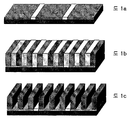
도 1의 1a-1c는 자기 정렬 공정을 도시한다.
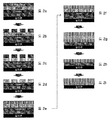
도 2의 2a-2i는 네거티브형 라인 증배를 위한 공정을 도시한다.
도 3의 3a-3g는 포지티브형 증배를 위한 공정을 도시한다.
도 4의 4a-4d는 컨택홀 공정을 도시한다.1a-1c in Fig. 1 show the self-alignment process.
2a-2i in Fig. 2 show a process for negative line doubling.
3a-3g of Fig. 3 show the process for positive multiplication.
4A-4D of Fig. 4 show the contact hole process.
본 발명은 신규의 중성층 조성물, 블록 공중합체의 유도 자기조립을 위한 중성층 형성을 위한 이의 용도, 및 고해상도 및 우수한 리소그래피 성질을 가진 패턴을 형성하기 위한 신규의 유도 자기조립 공정에 관한 것이다. 신규의 조성물은 블록 공중합체의 자기조립을 위해 사용하기 위한 중성층을 형성할 수 있다. 중성층은 중성층 위에 코팅된 블록 공중합체가 고해상도 리소그래피를 얻기 위해 기판에 대해 바람직한 방향으로 정렬되도록 하는 배향 제어층이다. 본 발명은 또한 블록 공중합체의 유도 자기조립에 사용하기 위한 신규의 공정, 예컨대 그라포에피택시 및 케모에피택시에 관한 것으로, 이는 중성층 조성물을 사용한다. 본 발명은 통상적인 리소그래피 기법, 예컨대 UV 리소그래피 (450 nm 내지 10nm), 액침 리소그래피, EUV 또는 e-빔에 의해 형성된 표적화된 특징부의 해상도 또는 CD 균일도에 있어 추가 개선을 제공한다. 본 발명은 하나 이상의 랜덤 가교성 중합체를 포함하는 중성층 조성물에 관한 것이다. 본 발명의 신규의 조성물에는 1종 초과의 중합체가 사용될 수 있다. 신규의 조성물은 단지 랜덤 공중합체(들)를 포함한다. 중합체는 유도 자기조립을 위해 사용된 블록 공중합체의 정렬에 대해 중립적인 상호작용을 가지지만, 중성층이 중성으로 남고 중성층 위에서 일어나는 공정, 예컨대 중성층 위에 코팅된 층과의 상호혼합, 현상, 광조사, 스트리핑, 등에 의해 악영향을 받지 않도록 하는 높은 정도로 가교될 수 있다. 신규의 중합체는 뜻밖에도 블록 공중합체에 대한 중성상태(neutrality)와 가교 둘다에 있어 최적 수준을 중성층에 제공하여 후속 공정으로 인한 중성층에 대한 원치않은 손상을 방지하는 것으로 나타났다. The present invention relates to a novel neutral layer composition, its use for neutral layer formation for the induced self-assembly of block copolymers, and a new inductive self-assembly process for forming patterns with high resolution and good lithographic properties. The novel compositions may form a neutral layer for use for self-assembly of block copolymers. The neutral layer is an orientation control layer that allows the block copolymer coated on the neutral layer to align in the desired direction relative to the substrate to obtain high resolution lithography. The present invention also relates to novel processes for use in the induction self-assembly of block copolymers, such as grapevaporation and chemoepitaxy, which use a neutral layer composition. The present invention provides further improvements in the resolution or CD uniformity of the targeted feature formed by conventional lithography techniques, such as UV lithography (450 nm to 10 nm), immersion lithography, EUV or e-beam. The present invention relates to a neutral layer composition comprising at least one randomly crosslinkable polymer. More than one polymer may be used in the novel compositions of the present invention. The novel compositions comprise only random copolymer (s). Polymers have neutral interactions with the alignment of the block copolymers used for inductive self-assembly, but the processes in which the neutral layer remains neutral and occur on the neutral layer, such as intermixing with the layer coated on the neutral layer, It can be crosslinked to a high degree to prevent it from being adversely affected by light irradiation, stripping, and the like. The new polymers have unexpectedly been found to provide optimal levels of neutrality and cross-linking for the block copolymer to the neutral layer to prevent unwanted damage to the neutral layer due to subsequent processing.
신규의 중성층 조성물은 하나 이상의 구조 단위 (1), 하나 이상의 구조 단위 (2) 및 하나 이상의 구조 단위 (3)을 가진 하나 이상의 랜덤 중합체를 포함한다:The novel neutral layer composition comprises at least one random polymer having at least one structural unit (1), at least one structural unit (2) and at least one structural unit (3)

상기 식에서 R1은 C1-C8 알킬, C1-C8 플루오로알킬, C1-C8 부분적으로 플루오르화된 알킬, C4-C8 사이클로알킬, C4-C8 사이클로플루오로알킬, C4-C8 부분적으로 플루오르화된 사이클로알킬, 및 C2-C8 히드록시알킬로 구성된 군으로부터 선택되고; R2, R3 및 R5는 H, C1-C4 알킬, CF3 및 F로 구성된 군으로부터 독립적으로 선택되고; R4는 H, C1-C8 알킬, C1-C8 부분적으로 플루오르화된 알킬 및 C1-C8 플루오로알킬로 구성된 군으로부터 선택되고, n은 1 내지 5 범위이고, R6은 H, F, C1-C8 알킬, C1-C8 플루오로알킬 및 C1-C8 부분적으로 플루오르화된 알킬로 구성된 군으로부터 선택되고 m은 1 내지 3 범위이다. 일 실시양태에서, R1은 C1-C8 알킬이고; R2, R3 및 R5는 H 및 C1-C4 알킬로 구성된 군으로부터 독립적으로 선택되고; R4는 H 및 C1-C8 알킬로 구성된 군으로부터 선택되고 n = 1; 및 R6은 H 및 C1-C8 알킬로 구성된 군으로부터 선택되고 m = 1. 또 다른 실시양태에서 R2, R3 및 R5 는 수소이고, R1은 C1-C8 알킬이고, R4 및 R6은 수소이다. 중성(neutral) 중합체는 구조식 (4)로 표시될 수 있으며, 여기서 x, y 및 z는 반복 단위의 몰%이다. 일 실시양태에서 x, y 및 z의 합은 100%이다.Wherein R 1 is selected from the group consisting of C 1 -C 8 alkyl, C 1 -C 8 fluoroalkyl, C 1 -C 8 partially fluorinated alkyl, C 4 -C 8 cycloalkyl, C 4 -C 8 cyclofluoroalkyl , C 4 -C 8 partially fluorinated cycloalkyl, and C 2 -C 8 hydroxyalkyl; R 2 , R 3 and R 5 are independently selected from the group consisting of H, C 1 -C 4 alkyl, CF 3 and F; R 4 is selected from the group consisting of H, C 1 -C 8 alkyl, C 1 -C 8 partially fluorinated alkyl and C 1 -C 8 fluoroalkyl, n ranges from 1 to 5, and R 6 is Is selected from the group consisting of H, F, C 1 -C 8 alkyl, C 1 -C 8 fluoroalkyl and C 1 -C 8 partially fluorinated alkyl and m ranges from 1 to 3. In one embodiment, R 1 is C 1 -C 8 alkyl; R 2 , R 3 and R 5 are independently selected from the group consisting of H and C 1 -C 4 alkyl; R 4 is selected from the group consisting of H and C 1 -C 8 alkyl and n = 1; And R 6 is selected from the group consisting of H and C 1 -C 8 alkyl and m = 1. In yet another embodiment, R 2, R 3 and R 5 are hydrogen, R 1 is C 1 -C 8 alkyl, R 4 and R 6 are hydrogen. The neutral polymer may be represented by the structural formula (4), wherein x, y, and z are mole percent of the repeating units. In one embodiment, the sum of x, y, and z is 100%.

신규의 랜덤 중합체는 알켄 함유 단량체가 랜덤 중합될 수 있는 다양한 방식으로 제조될 수 있지만(예컨대 니트록시드 매개 중합, 양이온, 음이온 축합 연쇄 중합 등) 일반적으로 라디칼 중합 예컨대 자유 라디칼 개시제 예컨대 AIBN(아조비스이소부티로니트릴), 벤조일 퍼옥시드 또는 다른 표준 써말 라디칼 개시제에 의해 개시된 라디칼 중합에 의해 제조된다. 이들 재료는 또한 기판 상에 말단 기를 통해 그라프팅함으로써 빗형상(comlike) 구조를 형성할 필요가 없지만 기판 표면으로의 공유 부착없이 통상적인 중합체와 같이 단순히 방사(spun)될 수 있다. 본 중합체는 바람직하게는, 구조 단위 3의 농도가 10 몰%를 초과하도록 합성되며; 뜻밖에도, 단위 (3)을 10 몰% 초과하여 가지면 블록 공중합체에 대한 중성을 파괴하지 않고 원치않은 공정 손상, 예컨대 포스트 적용 베이킹(post applied bake) 후 용매에 대한 중성막의 내성을 극적으로 증가시켜 유기 용매에서 검출가능한 막 손실을 나타내지 않는 이점을 가지는 것으로 밝혀졌다. 예전에는 블록 공중합체를 형성하는 공단량체의 랜덤화가 허용가능한 중성층 중합체를 제공하는 것으로 일반적으로 여겨졌고; 이에 따라 임의의 다른 공단량체 단위가 최소 농도, 전형적으로 대략 2몰%로 유지되었다. 신규의 중성층은 고도로 가교되어 그 위에 코팅된 블록 공중합체의 용액이 상호혼합을 일으키지 않고 예상치않게 블록 공중합체에 대해 중성으로 남는다. 뜻밖에도, 신규의 중성층의 중성은 통상의 리소그래피 공정 단계, 예컨대 레지스트 코팅, 레지스트 소프트 베이킹, 레지스트 노광, PEB, 레지스트 포지티브-형 및 레지스트 네거티브-형 현상, 및 유기 용매 및 TMAH 현상제를 이용한 레지스트 스트리핑에 대해 지속적이다. 이는 다시, 일반적으로 높은 포스트 적용 베이킹 온도(예컨대 200℃) 이후 조차 부분적으로 가교된 표면 재료를 제거할 필요가 있는 다수의 현행 중성층에서 요구되는 임의의 용매 처리 단계가 필요없도록 하는 이점을 가진다. 일반적으로, 약 2 몰% 초과의 가교 단위 (3)을 도입하면 자기조립 블록 공중합체에 대한 중성을 파괴하는 것으로 여겨졌다. 뜻밖에도 본 발명의 신규의 중합체는 10 몰% 초과의 구조 단위 (3)을 가짐에도 불구하고 자기조립 블록 공중합체에 대해 여전히 중성상태를 유지할 수 있는 높은 공정 저항막을 형성할 수 있다. 부가적으로, 뜻밖에도 신규의 조성물은 기판에 걸쳐 매우 우수한 막 균일도를 가진 가교된 중성층을 제공하고 이를 유지한다.The novel random polymers can be prepared in a variety of ways in which the alkene containing monomers can be randomly polymerized (e.g., nitroxide mediated polymerization, cation, anion condensation chain polymerization, etc.), but generally radical polymerization such as free radical initiators such as AIBN Isobutyronitrile), benzoyl peroxide, or other standard thermal radical initiators. These materials also do not need to form a comable structure by grafting through the end groups onto the substrate, but they can simply be spun like a conventional polymer without covalent attachment to the substrate surface. The polymer is preferably synthesized such that the concentration of the structural unit 3 exceeds 10 mol%; Unexpectedly, having more than 10 mol% of unit (3) does not destroy neutrality for the block copolymer and dramatically increases the resistance of the neutral membrane to the solvent after unwanted process damage, such as post applied bake, And exhibits no detectable film loss in the solvent. In the past, randomization of comonomers to form block copolymers has generally been regarded as providing an acceptable neutral layer polymer; Whereby any other comonomer units were kept at a minimum concentration, typically about 2 mol%. The new neutral layer is highly crosslinked so that solutions of the block copolymer coated thereon do not intermix and remain unexpectedly neutral to the block copolymer. Unexpectedly, the neutrality of the new neutral layer can be reduced by conventional lithographic processing steps such as resist coating, resist soft baking, resist exposure, PEB, resist positive-type and resist negative-type development, and resist stripping using organic solvents and TMAH developers . This again has the advantage of eliminating the need for any solvent treatment steps that are required in a number of current neutral layers that need to remove the partially cross-linked surface material, even after a generally high post application baking temperature (e.g., 200 < 0 > C). In general, it was believed that introducing more than about 2 mole% of crosslinking units (3) would destroy neutrality for self-assembled block copolymers. Unexpectedly, the novel polymers of the present invention can form a high process resistant film that still retains a neutral state for the self-assembled block copolymer despite having a structural unit (3) in excess of 10 mole%. Additionally, unexpectedly, the novel compositions provide and maintain a crosslinked neutral layer with very good film uniformity across the substrate.
본 발명의 조성물의 일 실시양태에서 중합체는 블록 공중합체에 대해 가교된 중성층을 형성할 수 있다. In one embodiment of the composition of the present invention, the polymer may form a crosslinked neutral layer for the block copolymer.
바람직한 실시양태에서 중합체는 포토레지스트용 유기 용매에서 용해되지 않는 가교된 중성층을 형성할 수 있다.In a preferred embodiment, the polymer may form a crosslinked neutral layer that is not soluble in the photoresist organic solvent.
추가의 바람직한 실시양태에서 중합체는 수성 알칼리 현상제에서 용해되지 않는 가교된 중성층을 형성할 수 있다.In further preferred embodiments, the polymer may form a crosslinked neutral layer that is not soluble in the aqueous alkaline developer.
본 발명의 조성물의 또 다른 실시양태에서 블록 공중합체는 산소를 포함하는 플라즈마에서 높은 에칭율을 가진 단량체 단위의 블록 및 낮은 에칭율을 가진 단량체 단위의 블록을 포함한다.In another embodiment of the composition of the present invention, the block copolymer comprises a block of monomer units having a high etch rate and a block of monomer units having a low etch rate in a plasma comprising oxygen.
본 발명의 조성물의 추가 실시양태에서 블록 공중합체는 용액에서 높은 제거율(removal rate)을 가진 단량체 단위의 블록 및 낮은 제거율(removable rate)을 가진 단량체 단위의 블록을 포함한다.In a further embodiment of the composition of the present invention, the block copolymer comprises a block of monomer units with a high removal rate in solution and a block of monomer units with a low removal rate.
일 실시양태에서 중성층은 단위 1, 2 및 3을 포함하고, 여기서 단위 1은 약 5 몰% 내지 약 90 몰% 범위이고; 단위 2는 약 5 몰% 내지 약 90 몰% 범위이고 단위 3은 약 10 몰% 내지 약 60 몰% 범위이다. 또 다른 실시양태에서 중성층은 단위 1, 2 및 3을 포함하고, 여기서 단위 1은 약 20 몰% 내지 약 80 몰% 범위이고; 단위 2는 약 20 몰% 내지 약 80 몰% 범위이고 단위 3은 약 15 몰% 내지 약 45 몰% 범위이다. 또 다른 실시양태에서 구조 단위 (3)은 10 몰% 내지 45 몰% 범위이다.In one embodiment, the neutral layer comprises units 1, 2 and 3, wherein unit 1 ranges from about 5 mol% to about 90 mol%; Unit 2 ranges from about 5 mol% to about 90 mol%, and unit 3 ranges from about 10 mol% to about 60 mol%. In another embodiment, the neutral layer comprises units 1, 2 and 3, wherein unit 1 ranges from about 20 mol% to about 80 mol%; Unit 2 ranges from about 20 mol% to about 80 mol%, and Unit 3 ranges from about 15 mol% to about 45 mol%. In yet another embodiment, the structural unit (3) is in the range of 10 mol% to 45 mol%.
본원에서, 알킬은 직쇄형 또는 분지형일 수 있는 포화 탄화수소 기(예를 들면, 메틸, 에틸, 프로필, 이소프로필, tert-부틸 등)를 지칭하고, 사이클로알킬은하나의 포화 사이클을 함유한 탄화수소(예를 들면, 사이클로헥실, 사이클로프로필, 사이클로펜틸 등)를 지칭하고, 플루오로알킬은 모든 수소가 불소에 의해 치환되어진 직쇄형 또는 분지형 포화 알킬 기를 지칭하고, 사이클로플루오로알킬은 모든 수소가 불소에 의해 치환되어진 사이클로알킬 기를 지칭하고, 부분적으로 플루오르화된 알킬은 수소들 중 일부가 불소로 치환되어진 직쇄형 또는 분지형 포화 알킬 기를 지칭하고, 부분적으로 플루오르화된 사이클로알킬은 수소들 중 일부가 불소로 치환되어진 사이클로알킬 기를 지칭하고, 히드로알킬은 하나 이상의 히드록실 모이어티로 치환된 알킬 또는 사이클로알킬(예를 들면, -CH2-CH2-OH, CH-CH(OH)-CH3 등)을 지칭한다.Herein, alkyl refers to a saturated hydrocarbon group (e.g., methyl, ethyl, propyl, isopropyl, tert-butyl, etc.), which may be linear or branched and the cycloalkyl refers to a hydrocarbon containing one saturation cycle Refers to straight-chain or branched saturated alkyl groups in which all hydrogens are replaced by fluorine, and < RTI ID = 0.0 > cyclofluoroalkyl < / RTI > Refers to a straight or branched saturated alkyl group in which some of the hydrogens have been replaced by fluorine and partially fluorinated cycloalkyl refers to a cycloalkyl group in which some of the hydrogens have been replaced by fluorine Refers to a cycloalkyl group substituted with fluorine, wherein the hydroxyalkyl is alkyl substituted with one or more hydroxyl moieties Refers to a cycloalkyl (for example, -CH 2 -CH 2 -OH, CH- CH (OH) -CH 3).
신규의 중합체는 단일 중합체로서, 또는 상이한 분자량, 벤조사이클로부텐 펜던트 기를 함유한 반복 단위(예를 들면, 4-비닐-벤조사이클로부텐 유도된 반복 단위)의 다양한 농도, 상이한 공단량체 비, 등을 가진 중합체들의 블렌드로서 사용될 수 있다. 벤조사이클로부텐 함유 단량체 단위는 또한 다양한 양의 다른 단량체 단위, 예를 들어, 스티렌 및 메틸메타크릴레이트 단위와 함께 사용될 수 있고 광범위 블렌딩 조성물에서 상응하는 반복 단위를 함유한 블록 공중합체에 대해 중성상태를 유지하면서 상당히 실질적으로 달라질 수 있다. 이는 예를 들면 상이한 반복 단위 비를 함유한 2종의 상이한 중성 중합체를 함유한 이성분(binary) 블렌드의 조성을 조절하여 반복적인 특징부 예컨대 L/S 또는 CH 패턴의 정해진 어레이에 대해 패턴수정 및/또는 패턴증배를 부여함에 있어 그라포에피택시 또는 케모에피택시와 같은 특정의 자기 직접 접근법의 효과성을 최대화함으로써 중성층을 최적화하도록 해준다. 단일 중합체가 또한 신규의 조성물에 사용될 수 있다. 본 발명의 일 실시양태에서 중성층 조성물은 신규의 중합체의 2 이상의 상이한 조성의 블렌드를 포함한다. 조성물은 구조 단위 1, 2 및 3의 상이한 몰% 농도의 2 이상의 중합체의 블렌드를 포함할 수 있다. 예를 들어, 조성물은 단량체 단위의 상이한 몰비의 제1 및 제2 중합체를 포함하고; 제1 중합체는 구조 단위 1이 약 5 몰% 내지 약 90 몰%이고, 구조 단위 2가 약 5 몰% 내지 약 90 몰%이고 구조 3이 약 10 몰% 내지 약 60 몰%인 중합체이고; 제2 중합체는 구조 단위 1이 약 5 몰% 내지 약 90 몰%이고, 구조 단위 2가 약 5 몰% 내지 약 90 몰%이고 구조 3이 약 10 몰% 내지 약 60 몰%인 중합체이다.The novel polymers can be used as homopolymers or with different molecular weights, with varying concentrations of repeating units containing benzocyclobutene pendant groups (e.g., 4-vinyl-benzocyclobutene derived repeat units), different comonomer ratios, etc. Can be used as a blend of polymers. The benzocyclobutene-containing monomer units may also be used in conjunction with varying amounts of other monomer units, such as styrene and methyl methacrylate units, and have a neutral state for block copolymers containing corresponding repeating units in a wide range of blending compositions But can vary substantially substantially. This may be achieved, for example, by modifying the composition of a binary blend containing two different neutral polymers containing different repeating unit ratios to modify and / or modify the patterned array of repeating features, e.g., L / S or CH patterns, Or to maximize the effectiveness of certain self-directed approaches, such as graphexepitaxy or chemo-epitaxy, in imparting pattern multiplication, thereby optimizing the neutral layer. Homopolymers can also be used in the novel compositions. In one embodiment of the present invention, the neutral layer composition comprises a blend of two or more different compositions of the novel polymer. The composition may comprise a blend of two or more polymers of different mol% concentrations of structural units 1, 2 and 3. For example, the composition comprises first and second polymers in different molar ratios of monomer units; The first polymer is a polymer wherein from about 5 mol% to about 90 mol% structural unit 1, from about 5 mol% to about 90 mol% structural unit 2 and from about 10 mol% to about 60 mol% structure 3; The second polymer is a polymer wherein from about 5 mole% to about 90 mole% structural unit 1, from about 5 mole% to about 90 mole% structural unit 2 and from about 10 mole% to about 60 mole% structure 3 is present.
중성층 조성물의 고체 성분은 고체 성분을 용해시키는 용매 또는 용매들의 혼합물과 혼합된다. 적당한 용매는 예를 들어, 글리콜 에테르 유도체 예컨대 에틸 셀로솔브, 메틸 셀로솔브, 프로필렌 글리콜 모노메틸 에테르(PGME), 디에틸렌 글리콜 모노메틸 에테르, 디에틸렌 글리콜 모노에틸 에테르, 디프로필렌 글리콜 디메틸 에테르, 프로필렌 글리콜 n-프로필 에테르, 또는 디에틸렌 글리콜 디메틸 에테르; 글리콜 에테르 에스테르 유도체 예컨대 에틸 셀로솔브 아세테이트, 메틸 셀로솔브 아세테이트, 또는 프로필렌 글리콜 모노메틸 에테르 아세테이트(PGMEA); 카르복실레이트 예컨대 에틸 아세테이트, n-부틸 아세테이트 및 아밀 아세테이트; 디베이직산의 카르복실레이트 예컨대 디에틸옥실레이트 및 디에틸말로네이트; 글리콜의 디카르복실레이트 예컨대 에틸렌 글리콜 디아세테이트 및 프로필렌 글리콜 디아세테이트; 및 히드록시 카르복실레이트 예컨대 메틸 락테이트, 에틸 락테이트(EL), 에틸 글리콜레이트, 및 에틸-3-히드록시 프로피오네이트; 케톤 에스테르 예컨대 메틸 피루베이트 또는 에틸 피루베이트; 알콕시카르복실산 에스테르 예컨대 메틸 3-메톡시프로피오네이트, 에틸 3-에톡시프로피오네이트, 에틸 2-히드록시-2-메틸프로피오네이트, 또는 메틸에톡시프로피오네이트; 케톤 유도체 예컨대 메틸 에틸 케톤, 아세틸 아세톤, 사이클로펜타논, 사이클로헥사논 또는 2-헵타논; 케톤 에테르 유도체 예컨대 디아세톤 알콜 메틸 에테르; 케톤 알콜 유도체 예컨대 아세톨 또는 디아세톤 알콜; 케탈 또는 아세탈 예컨대 1,3 디옥살란 및 디에톡시프로판; 락톤 예컨대 부티로락톤; 아마이드 유도체 예컨대 디메틸아세트아마이드 또는 디메틸포름아마이드, 아니솔, 및 이의 혼합물을 포함할 수 있다. 조성물은 첨가제 예컨대 계면활성제를 더 포함할 수 있다.The solid component of the neutral layer composition is mixed with a solvent or a mixture of solvents to dissolve the solid component. Suitable solvents include, for example, glycol ether derivatives such as ethyl cellosolve, methyl cellosolve, propylene glycol monomethyl ether (PGME), diethylene glycol monomethyl ether, diethylene glycol monoethyl ether, dipropylene glycol dimethyl ether, propylene glycol n-propyl ether, or diethylene glycol dimethyl ether; Glycol ether ester derivatives such as ethyl cellosolve acetate, methyl cellosolve acetate, or propylene glycol monomethyl ether acetate (PGMEA); Carboxylates such as ethyl acetate, n-butyl acetate and amyl acetate; Carboxylates of dibasic acid such as diethyloxylate and diethylmalonate; Dicarboxylates of glycols such as ethylene glycol diacetate and propylene glycol diacetate; And hydroxycarboxylates such as methyl lactate, ethyl lactate (EL), ethyl glycolate, and ethyl-3-hydroxypropionate; Ketone esters such as methyl pyruvate or ethyl pyruvate; Alkoxycarboxylic acid esters such as methyl 3-methoxypropionate, ethyl 3-ethoxypropionate, ethyl 2-hydroxy-2-methylpropionate, or methyl ethoxypropionate; Ketone derivatives such as methyl ethyl ketone, acetylacetone, cyclopentanone, cyclohexanone or 2-heptanone; Ketone ether derivatives such as diacetone alcohol methyl ether; Ketone alcohol derivatives such as acetol or diacetone alcohol; Ketals or acetals such as 1,3 dioxolane and diethoxypropane; Lactones such as butyrolactone; Amide derivatives such as dimethylacetamide or dimethylformamide, anisole, and mixtures thereof. The composition may further comprise an additive such as a surfactant.
신규의 중성층 조성물은 기판 상에 코팅되고 가열되어 용매를 제거하고 막을 가교결합시킨다. 전형적인 막 두께는 가열 후 약 3 nm 내지 약 50 nm, 또는 약 3 nm 내지 약 30nm, 또는 약 4 nm 내지 약 20nm, 또는 약 5 nm 내지 약 20nm, 또는 약 10 nm 내지 약 20 nm 범위이다. 막은 약 180℃ 내지 약 350℃, 또는 약 200℃ 내지 약 300℃ 범위의 온도에서 가열될 수 있다. 일단 가교된 막이 형성되면 임의의 유도 자기조립 기법을 사용하여 최종적으로 패턴을 형성하기 위한 코팅은 추가 가공처리를 위해 사용될 수 있다. 이러한 기법의 예는 그라포에피택시, 표준 케모에피택시, 피닝을 이용한 케모에피택시, 등이다. 신규의 중성층 조성물에 의해 형성된 가교된 중성층은 가교된 중성층이 사용되는 리소그래피 공정, 예컨대 유기 용매(예컨대 중성층 위에 코팅을 형성하기 위해 사용된 용매, 용매 현상제, 등)로부터 용해, 수성 알칼리 현상제에서 용해, 중성층 위에 코팅된 포토레지스트를 이미지화 하는데 사용된 공정(예컨대 e-빔, euv, 원자외선, 등)으로부터의 손상, 또는 포토레지스트 스트리퍼에서의 용해 동안 발생할 수 있는 임의의 손상에도 불구하고 중성을 유지한다. 가교된 층은 용매 예컨대 포토레지스트를 코팅하는데 사용된 용매, 예컨대 PGMEA, PGME, EL, 등에 용해되지 않는다.The new neutral layer composition is coated on a substrate and heated to remove the solvent and crosslink the membrane. Typical film thicknesses range from about 3 nm to about 50 nm, or from about 3 nm to about 30 nm, or from about 4 nm to about 20 nm, or from about 5 nm to about 20 nm, or from about 10 nm to about 20 nm after heating. The film may be heated at a temperature in the range of from about 180 캜 to about 350 캜, or from about 200 캜 to about 300 캜. Once a crosslinked film is formed, a coating to finally form the pattern using any inductive self-assembly technique can be used for further processing. Examples of such techniques are grapevoefaciq, standard chemo phacaciqs, chemo phaciqs using pinning, and the like. The crosslinked neutral layer formed by the novel neutral layer composition can be obtained by a lithographic process in which a crosslinked neutral layer is used, for example, by dissolving from an organic solvent (such as a solvent used to form a coating on a neutral layer, a solvent developer, etc.) (E-beam, euv, far ultraviolet, etc.) used to image the photoresist coated on the neutral layer, or any damage that may occur during dissolution in the photoresist stripper But maintain neutrality. The crosslinked layer is not soluble in solvents used for coating solvents, such as photoresist, such as PGMEA, PGME, EL, and the like.
신규의 중성층 조성물과 함께 유도 자기조립에서 사용하기 위한 블록 공중합체는 자기조립을 통해 도메인을 형성할 수 있는 임의의 블록 공중합체일 수 있다. 마이크로도메인이 자기 회합 성향이 있는 동일 타입의 블록에 의해 형성된다. 전형적으로, 이러한 목적을 위해 이용된 블록 공중합체는 단량체에서 유도된 반복 단위가 조성, 구조 또는 둘다에 있어 상이하고 상분리 및 도메인 형성이 가능한 블록으로 배열되는 중합체이다. 블록은 나머지 블록을 표면 상에서 온전하게 유지하면서 일 블록을 제거하는데 사용될 수 있는 상이한 특성을 가지고 있어서, 표면 상에 패턴을 제공한다. 따라서, 블록은 플라즈마 에칭, 용매 에칭, 알칼리 수용액을 이용한 현상제 에칭, 등에 의해 선택적으로 제거될 수 있다. 유기 단량체 기제(based) 블록 공중합체에서, 하나의 블록이 폴리디엔, 폴리(알킬렌 옥시드), 예컨대 폴리(에틸렌 옥시드), 폴리(프로필렌 옥시드), 폴리(부틸렌 옥시드)을 포함한 폴리에테르 또는 이의 혼합물을 포함한 폴리올레핀계 단량체로부터 제조될 수 있고; 다른 블록이 폴리((메트)아크릴레이트), 폴리스티렌, 폴리에스테르, 폴리유기실록산, 폴리유기게르만(polyorganogermanes), 및/또는 이의 혼합물을 포함한 다른 단량체로부터 제조될 수 있다. 중합체 사슬에서 이들 블록은 각각 단량체에서 유도된 하나 이상의 반복 단위를 포함한다. 필요한 패턴의 종류 및 사용되는 방법에 따라 다양한 타입의 블록 공중합체가 사용될 수 있다. 예를 들어, 이들은 디블록 공중합체, 트리블록 공중합체, 삼원중합체(terpolymer), 또는 멀티블록 공중합체로 구성될 수 있다. 이들 블록 공중합체의 블록은 그 자체로 단독중합체 또는 공중합체로 구성될 수 있다. 자기조립을 위해 다양한 타입의 블록 공중합체, 예컨대 수지상 블록 공중합체, 과분지화된 블록 공중합체, 그라프트 블록 공중합체, 유기 디블록 공중합체, 유기 멀티블록 공중합체, 직쇄형 블록 공중합체, 별모양 블록 공중합체, 양친매성 무기 블록 공중합체, 양친매성 유기 블록 공중합체 또는 적어도 상이한 타입의 블록 공중합체로 구성된 혼합물이 이용될 수 있다.The block copolymer for use in induced self-assembly with the novel neutral layer composition may be any block copolymer capable of forming a domain through self-assembly. The microdomains are formed by blocks of the same type with self-association tendencies. Typically, the block copolymers used for this purpose are polymers in which the repeat units derived from the monomers are arranged in blocks that are different in composition, structure, or both and are capable of phase separation and domain formation. The block has different characteristics that can be used to remove one block while keeping the remaining blocks intact on the surface, thus providing a pattern on the surface. Thus, the block can be selectively removed by plasma etching, solvent etching, developer etching using an aqueous alkaline solution, and the like. In organic monomer based block copolymers, one block is a block copolymer comprising a poly (diene), a poly (alkylene oxide) such as poly (ethylene oxide), poly (propylene oxide), poly (butylene oxide) May be prepared from polyolefin-based monomers including polyethers or mixtures thereof; Other blocks may be made from other monomers including poly ((meth) acrylate), polystyrene, polyester, polyorganosiloxane, polyorganogermanes, and / or mixtures thereof. In the polymer chain, each of these blocks contains at least one repeating unit derived from a monomer. Various types of block copolymers may be used depending on the type of pattern required and the method used. For example, they may be comprised of diblock copolymers, triblock copolymers, terpolymers, or multiblock copolymers. The blocks of these block copolymers may themselves be composed of homopolymers or copolymers. For self-assembly, various types of block copolymers such as dendritic block copolymers, hyperbranched block copolymers, graft block copolymers, organic diblock copolymers, organic multi-block copolymers, linear block copolymers, Mixtures of block copolymers, amphipathic inorganic block copolymers, amphiphilic organic block copolymers, or at least different types of block copolymers may be used.
유기 블록 공중합체의 블록은 단량체 예컨대 C2-30 올레핀, C 1-30 알콜에서 유도된 (메트)아크릴레이트 단량체, Si, Ge, Ti, Fe, Al에 기초한 단량체를 포함한 무기-함유 단량체에서 유도된 반복 단위를 포함할 수 있다. C2-30 올레핀 기제 단량체는 단독으로 높은 내에칭성 블록을 구성하거나, 또는 하나의 다른 올레핀계 단량체와 함께 그렇게 할 수 있다. 이러한 타입의 올레핀계 단량체의 구체적인 예는 에틸렌, 프로필렌, 1-부텐, 1,3-부타디엔, 이소프렌, 디하이드로피란, 노르보르넨, 말레산 무수물, 스티렌, 4-히드록시 스티렌, 4-아세톡시 스티렌, 4-메틸스티렌, 알파-메틸스티렌 또는 이의 혼합물이다. 고에칭성 단위의 예는 (메트)아크릴레이트 단량체 예컨대 (메트)아크릴레이트, 메틸 (메트)아크릴레이트, 에틸 (메트)아크릴레이트, n-프로필 (메트)아크릴레이트, 이소프로필 (메트)아크릴레이트, n-부틸 (메트)아크릴레이트, 이소부틸 (메트)아크릴레이트, n-펜틸 (메트)아크릴레이트, 이소펜틸 (메트)아크릴레이트, 네오펜틸 (메트)아크릴레이트, n-헥실 (메트)아크릴레이트, 사이클로헥실 (메트)아크릴레이트, 이소보르닐 (메트)아크릴레이트, 히드록시에틸 (메트)아크릴레이트 또는 이의 혼합물에서 유도될 수 있다.The block of the organic block copolymer is derived from an inorganic-containing monomer containing monomers based on monomers such as C 2-30 olefins, (meth) acrylate monomers derived from C 1-30 alcohol, Si, Ge, Ti, Lt; / RTI > repeat units. The C 2-30 olefin base monomers can be made by themselves either as a high etch resistant block or together with one other olefin based monomer. Specific examples of these types of olefin monomers include ethylene, propylene, 1-butene, 1,3-butadiene, isoprene, dihydropyran, norbornene, maleic anhydride, styrene, 4-hydroxystyrene, 4- Styrene, 4-methylstyrene, alpha-methylstyrene or mixtures thereof. Examples of the high-etch unit include (meth) acrylate monomers such as (meth) acrylate, methyl (meth) acrylate, ethyl (meth) acrylate, n-propyl (meth) acrylate, (meth) acrylate, n-butyl (meth) acrylate, isobutyl (meth) acrylate, n-pentyl (Meth) acrylate, isobornyl (meth) acrylate, hydroxyethyl (meth) acrylate, or mixtures thereof.
일종의 높은 내에칭성 반복 단위를 함유한 블록 공중합체의 일례는 스티렌에서 유도된 반복 단위만을 함유한 폴리스티렌 블록, 및 메틸메타크릴레이트에서 유도된 반복 단위만을 함유한 또 다른 타입의 고에칭성 폴리메틸메타크릴레이트 블록이다. 이들은 함께 블록 공중합체 폴리(스티렌-b-메틸메타크릴레이트)를 형성하고, 여기서 b는 블록을 지칭한다.An example of a block copolymer containing a kind of high-etch repetitive units is a polystyrene block containing only a repeating unit derived from styrene, and another type of high-etch polymethyl methacrylate containing only repeating units derived from methyl methacrylate Methacrylate block. Together they form a block copolymer poly (styrene-b-methyl methacrylate), where b refers to the block.
패턴화된 중성층 상에서 유도 자기조립을 위해 사용시 그라포에피택시, 케모에피택시 또는 피닝된 케모에피택시를 위해 유용한 블록 공중합체의 구체적인 비제한적인 예는, 폴리(스티렌-b-비닐 피리딘), 폴리(스티렌-b-부타디엔), 폴리(스티렌-b-이소프렌), 폴리(스티렌-b-메틸 메타크릴레이트), 폴리(스티렌-b-알케닐 방향족 화합물), 폴리(이소프렌-b-에틸렌 옥시드), 폴리(스티렌-b-(에틸렌-프로필렌)), 폴리(에틸렌 옥시드-b-카프로락톤), 폴리(부타디엔-b-에틸렌 옥시드), 폴리(스티렌-b-t-부틸 (메트)아크릴레이트), 폴리(메틸 메타크릴레이트-b-t-부틸 메타크릴레이트), 폴리(에틸렌 옥시드-b-프로필렌 옥시드), 폴리(스티렌-b-테트라하이드로퓨란), 폴리(스티렌-b-이소프렌-b-에틸렌 옥시드), 폴리(스티렌-b-디메틸실록산), 폴리(메틸 메타크릴레이트-b-디메틸실록산), 또는 상술한 블록 공중합체 중 하나 이상을 포함하는 조합이다. 이러한 모든 중합체 재료는 전형적으로 IC 소자 제조에 이용되는 에칭 기법에 내성인 반복 단위가 풍부한 하나 이상의 블록과 이러한 동일 조건 하에 빠르게 에칭되는 하나 이상의 블록의 존재를 공유한다. 이는 유도 자기조립된 중합체가 기판 상으로 패턴 전사하도록 허락하고 이에 따라 패턴수정 또는 패턴증배에 영향을 준다.Specific non-limiting examples of block copolymers useful for grapefy-epitaxy, chemo-epitaxy or pinned chemo-epitaxy when used for induction self-assembly on a patterned neutral layer include poly (styrene-b-vinylpyridine B-isoprene), poly (styrene-b-methyl methacrylate), poly (styrene-b-alkenyl aromatic compound), poly (isoprene-b- Ethylene oxide), poly (styrene-b- (ethylene-propylene)), poly (ethylene oxide-b-caprolactone), poly (butadiene- (Meth) acrylate), poly (methyl methacrylate-butyl methacrylate), poly (ethylene oxide-b-propylene oxide), poly (styrene-b-tetrahydrofuran) Isoprene-b-ethylene oxide), poly (styrene-b-dimethylsiloxane), poly (methyl methacrylate-b- ), Or the above-mentioned block a combination comprising one or more of the copolymer. All of these polymeric materials typically share the presence of one or more blocks rich in repeat units resistant to etching techniques used in IC device fabrication and one or more blocks that are quickly etched under these same conditions. This allows the induction self-assembled polymer to pattern transfer onto the substrate and thus affect pattern modification or pattern multiplication.
전형적으로, 예컨대 그라포에피택시, 케모에피택시 또는 피닝된 케모에피택시에서 유도 자기조립에 이용된 블록 공중합체는, 중량-평균 분자량(Mw)이 약 3,000 내지 약 500,000 g/mol 범위이고 수 평균 분자량(Mn)이 약 1,000 내지 약 60,000 이며, 다분산도(polydispersity)(Mw/Mn)가 약 1.01 내지 약 6, 또는 1.01 내지 약 2 또는 1.01 내지 약 1.5 이다. 분자량, Mw 및 Mn은 둘다 폴리스티렌 표준으로 보정되는 범용 보정 방법을 사용하여 예를 들어, 겔 투과 크로마토그래피에 의해 측정될 수 있다. 이는, 정해진 표면에 자발적으로, 또는 순수한 열처리를 사용함으로써, 또는 자기조립이 일어나도록 하는 세그먼트의 흐름을 증가시키기 위해 중합체 골격 안으로 용매 증기의 흡수에 의해 보조되는 열처리 공정을 통해 적용되는 경우 중합체 블록이 자기조립이 이루어지도록 충분한 이동성을 가지도록 해준다.Typically, for example Gras Four epitaxy, Kane Moe blood taxi or pinned Kane Moe blocks used for inducing self-assembly in the blood taxi copolymer, weight-average molecular weight (M w) of about 3,000 to about 500,000 g / mol range And a number average molecular weight (M n ) of from about 1,000 to about 60,000 and a polydispersity (M w / M n ) of from about 1.01 to about 6, or from 1.01 to about 2 or from 1.01 to about 1.5. The molecular weights, M w and M n , can be measured, for example, by gel permeation chromatography using a universal calibration method in which both are corrected to polystyrene standards. This can be achieved by applying a volumetric or pure heat treatment to a defined surface or through a heat treatment process assisted by the absorption of solvent vapor into the polymer backbone to increase the flow of the segment to cause self- And has sufficient mobility to allow self-assembly.
막 형성을 위해 블록 공중합체를 용해시키기에 적합한 용매는 블록 공중합체의 용해도 요건이 달라질 수 있다. 블록 공중합체 조립용 용매의 예는 프로필렌 글리콜 모노메틸 에테르 아세테이트(PGMEA), 에톡시에틸 프로피오네이트, 아니솔, 에틸 락테이트, 2-헵타논, 사이클로헥사논, 아밀 아세테이트, n-부틸 아세테이트, n-아밀 케톤(MAK), 감마-부티로락톤(GBL), 톨루엔, 등을 포함한다. 일 실시양태에서, 특히 유용한 캐스팅 용매는 프로필렌 글리콜 모노메틸 에테르 아세테이트(PGMEA), 감마-부티로락톤(GBL), 또는 이들 용매의 조합을 포함한다. Solvents suitable for dissolving the block copolymer for film formation may vary in solubility requirements of the block copolymer. Examples of the solvent for assembling the block copolymer include propylene glycol monomethyl ether acetate (PGMEA), ethoxyethyl propionate, anisole, ethyl lactate, 2-heptanone, cyclohexanone, amyl acetate, amyl ketone (MAK), gamma-butyrolactone (GBL), toluene, and the like. In one embodiment, particularly useful casting solvents include propylene glycol monomethyl ether acetate (PGMEA), gamma-butyrolactone (GBL), or a combination of these solvents.
블록 공중합체 조성물은 무기-함유 중합체; 소분자, 무기-함유 분자, 계면활성제, 광산 발생제, 열산 발생제, 퀀처(quenchers), 경화제, 가교제, 사슬 연장제, 등을 포함한 첨가제; 및 상기의 하나 이상을 포함하는 조합으로 구성된 군으로부터 선택된 부가적인 성분 및/또는 첨가제를 포함할 수 있고, 부가적인 성분 및/또는 첨가제의 하나 이상이 블록 공중합체와 함께 조립되어 블록 공중합체 어셈블리를 형성한다.The block copolymer composition comprises an inorganic-containing polymer; Additives including small molecules, inorganic molecules, surfactants, photoacid generators, thermal acid generators, quenchers, hardeners, crosslinking agents, chain extenders, and the like; And combinations comprising at least one of the foregoing, and wherein at least one of the additional components and / or additives is assembled with the block copolymer to form a block copolymer assembly .
블록 공중합체 조성물은 통상적인 리소그래피에 의해 표면 상에 규정되어진 신규의 중성층 패턴에 도포(적용)되며, 여기서 중성 표면은 신규의 조성물로부터 형성된 가교된 코팅이다. 도포 및 용매 제거 시에, 블록 공중합체는 이후, 통상적인 리소그래피 공정에 의해 형성된 기판 표면의 패턴화된 화학적 차이 또는 실제 토포그래피 특징부를 통해 중성층 위에 통상적인 리소그래피 공정에 의해 형성된 특정 패턴에 의해 유도된 자기조립을 겪는다. 패턴 전사를 위해 표준 IC 공정 후 마이크로상 분리 거리에 대한 패턴의 상대적인 피치에 의존하여, 동일 해상도를 유지하는 패턴수정이 달성되고/되거나, 복수 상 경계가 통상적인 리소그래피로 한정된 특징부들 사이에 형성되면 패턴증배가 또한 달성될 수 있다.The block copolymer composition is applied to the new neutral layer pattern defined on the surface by conventional lithography, wherein the neutral surface is a crosslinked coating formed from the novel composition. Upon application and solvent removal, the block copolymer is then subjected to a patterning chemical difference of the substrate surface formed by a conventional lithographic process, or by a specific pattern formed by a conventional lithographic process on the neutral layer through actual topographic features Self-assembly. Depending on the relative pitch of the pattern relative to the microphotographic separation distance after the standard IC process for pattern transfer, pattern modification to maintain the same resolution is achieved and / or when multiple phase boundaries are formed between the features defined by conventional lithography Pattern multiplication can also be achieved.
(스핀 건조를 포함한) 스피닝 기법에 의한 블록 공중합체의 도포가 자기 유도 블록 공중합체 어셈블리를 형성하기에 충분할 수 있다. 자기 유도 도메인 형성의 다른 방법은 도포, 베이킹, 어닐링 동안, 또는 이들 작업 중 하나 이상의 조합 동안 이루어질 수 있다. 이러한 방식으로, 배향된 블록 공중합체 어셈블리는 상기 방법에 의해 제조되고, 중성 표면에 수직으로 배향된 원통형 마이크로도메인을 포함하거나, 또는 중성 표면에 수직으로 배향된 라멜라 도메인을 포함하는 마이크로상(microphase)-분리된 도메인을 가진다. 일반적으로, 마이크로상-분리된 도메인은 중성 표면에 수직으로 배향된 라멜라 도메인이고, 블록 공중합체 어셈블리에서 평행한 라인/스페이스 패턴을 제공한다. 이렇게 배향된 도메인은 바람직하게도 추가 공정 조건 하에 열적으로 안정하다. 따라서, 유용한 디블록 공중합체, 예를 들어, 폴리(스티렌-b-메틸메타크릴레이트)를 포함한 블록 공중합체 어셈블리 층의 코팅, 및 경우에 따라 베이킹 및/또는 어닐링 후, 블록 공중합체의 도메인이 중성 표면 상에 형성될 것이고 중성 표면에 대해 수직으로 남게 되어, 기판 표면 상에 높은 내에칭성 및 고에칭성 영역을 제공하고, 이는 기판 층에 추가로 패턴 전사될 수 있다. 유도 자기조립된 블록 공중합체 패턴은 공지의 기법을 사용하여 하부(underlying) 기판에 전사된다. 일례에서 습식 또는 플라즈마 에칭이 선택적 UV 노광과 함께 사용될 수 있다. 습식 에칭은 아세트산으로 실시될 수 있다. 표준 플라즈마 에칭 공정, 예컨대 산소를 포함하는 플라즈마가 사용될 수 있고; 부가적으로 아르곤, 일산화탄소, 이산화탄소, CF4, CHF3가 플라즈마에 존재할 수 있다. 도 1a-1c는 중성층을 개질하여 패턴화된 화학적 친화성을 규정하는 공정을 도시한다(도 1a). 이후, 블록 공중합체가 화학적으로 개질된 중성층 위에 코팅되고 어닐링되어 기판 표면에 수직인 도메인을 형성한다(도 1b). 이후 도메인들중 하나를 제거하여 기판 표면 상에 패턴을 형성한다(도 1c).Application of the block copolymer by a spinning technique (including spin drying) may be sufficient to form a magnetic induction block copolymer assembly. Other methods of magnetic induction domain formation may occur during application, baking, annealing, or during one or more combinations of these operations. In this way, an oriented block copolymer assembly is produced by the method and comprises a cylindrical microdomain oriented perpendicular to the neutral surface, or a microphase comprising a lamellar domain oriented vertically to the neutral surface, - Have separate domains. Generally, the microphase-separated domain is a lamellar domain oriented perpendicular to the neutral surface and provides a parallel line / space pattern in the block copolymer assembly. The domains thus oriented are preferably thermally stable under further processing conditions. Thus, after coating a block copolymer assembly layer containing useful diblock copolymers such as poly (styrene-b-methyl methacrylate), and optionally baking and / or annealing, the domain of the block copolymer Will be formed on the neutral surface and will remain perpendicular to the neutral surface, providing a high etchability and high etchability region on the substrate surface, which can be further pattern transferred to the substrate layer. The induced self-assembled block copolymer pattern is transferred to the underlying substrate using known techniques. In one example, a wet or plasma etch may be used with selective UV exposure. Wet etching may be performed with acetic acid. A standard plasma etch process, such as a plasma containing oxygen, may be used; Additionally, it is argon, carbon monoxide, carbon dioxide, CF 4, CHF 3 may be present in the plasma. Figures 1A-1C illustrate a process for modifying the neutral layer to define the patterned chemical affinity (Figure 1A). The block copolymer is then coated over the chemically modified neutral layer and annealed to form a domain perpendicular to the substrate surface (FIG. 1B). One of the domains is then removed to form a pattern on the substrate surface (FIG. 1C).
본 발명에서 유도 자기조립 패턴 형성을 위해 사용된 초기 포토레지스트 패턴은 네거티브 또는 포지티브 포토레지스트, 또는 포지티브형 또는 네거티브형 현상 공정을 사용하여 규정될 수 있고, 임의의 통상적인 리소그래피 기법, 예컨대 e-빔, 이온 빔, x-선, EUV(13.5 nm), 광대역(broadband), 또는 UV(450 nm-10 nm) 노광, 액침 리소그래피, 등을 사용하여 이미지형성 가능하다. 일 실시양태에서 본 발명은 건식 리소그래피 또는 액침 리소그래피를 사용하여 193nm 이미지방식(imagewise) 노광에 특히 유용하다. 193 nm 리소그래피의 경우 시판되는 포지티브 193 nm 포토레지스트, 예컨대 비제한적인 예로서 AZ AX2110P(AZ Electronic Materials USA Corp, 뉴저지주 서머빌 소재), Shin-Etsu Chemical Corp.의 포토레지스트, JSR Micro(Japan Synthetic Rubber에서 입수), 및 FujiFilm에서 입수가능한 다른 포토레지스트, TOK 등이 사용될 수 있다. 이들 포토레지스트는 노광 후 현상될 수 있고, 테트라메틸암모늄 히드록시드를 포함한 수성 알칼리 현상제를 사용하여 노광후 베이킹되어 포지티브형 패턴을 형성하거나 유기 용매 예컨대 n-아밀 케톤(MAK), n-부틸 아세테이트, 아니솔, 등을 사용하여 현상되어 네거티브형 패턴을 형성할 수 있다. 대안으로, 또한 193 nm 노광의 경우, 시판되는 네거티브형 포토레지스트가 이용될 수 있다. 본 발명의 일 특별한 특징은 중성층의 높은 가교 수준에도 불구하고, 예기치 않게도 블록 공중합체에 대한 중성층의 중성상태가 유지되는데 있다. 높은 수준의 가교는 공정 단계, 예컨대 포토레지스트를 이용한 오버코팅, 포토레지스트의 베이킹, 포토레지스트의 노광, 포토레지스트의 각 타입에 대해 상술한 바와 같이 사용되는 현상제를 이용한 포토레지스트 패턴의 현상, 스트리핑 조건, 등이 실시되는 경우 필요하지만; 신규의 중성막은 여전히 중성상태를 보유하고 있어 토포그래픽 리소그래피 특징부들 사이의 블록 공중합체 도메인의 적절한 배향을 가능하게 한다. 도 1a-1c에 도시된 바와 같이, 블록 공중합체의 도메인이 중성 표면 상에 형성되면서 중성 표면에 대해 수직으로 남도록, 정렬 공정 동안 블록 공중합체의 배향을 제어하도록 중성상태가 요구된다. 도 1a-1c는 블록 공중합체가 자체적으로 기판에 수직인 도메인으로 배향하는 방법과 도메인 중 하나가 제거되어 기판 상에 패턴을 형성하는 방법을 도시한다.The initial photoresist pattern used for forming the induced self-assembled pattern in the present invention may be defined using a negative or positive photoresist, or a positive or negative development process, and may be formed using any conventional lithography technique, , Ion beam, x-ray, EUV (13.5 nm), broadband, or UV (450 nm-10 nm) exposure, immersion lithography, In one embodiment, the invention is particularly useful for 193 nm imagewise exposures using dry lithography or immersion lithography. Commercially available positive 193 nm photoresists for 193 nm lithography such as AZ AX2110P (AZ Electronic Materials USA Corp, Summerville, NJ), photoresist from Shin-Etsu Chemical Corp., JSR Micro (Japan Synthetic Rubber), and other photoresists available from FujiFilm, TOK, and the like. These photoresists can be developed after exposure and baked after exposure using an aqueous alkaline developer containing tetramethylammonium hydroxide to form a positive pattern or an organic solvent such as n-amyl ketone (MAK), n-butyl Acetate, anisole, or the like, so that a negative pattern can be formed. Alternatively, for a 193 nm exposure, a commercially available negative photoresist may be used. One particular feature of the present invention is that, despite the high crosslinking level of the neutral layer, unexpectedly, the neutral state of the neutral layer for the block copolymer is maintained. The high level of crosslinking can be achieved through process steps such as overcoating using photoresist, baking photoresist, exposure of photoresist, development of photoresist patterns using a developer used for each type of photoresist, stripping Condition, etc., is necessary; The new neutral film still retains a neutral state to enable proper orientation of the block copolymer domains between the topographic lithography features. A neutral state is required to control the orientation of the block copolymer during the alignment process so that the domains of the block copolymer are formed on the neutral surface and remain perpendicular to the neutral surface, as shown in Figures 1A-1C. Figures 1A-1C illustrate how the block copolymer itself is oriented in a domain perpendicular to the substrate and how one of the domains is removed to form a pattern on the substrate.
중성층이 코팅되는 기판은 소자에 의해 임의로 요구된다. 일례에서 기판은 규소 또는 티타늄 함유 ARC(산소 플라즈마에 대한 높은 내에칭성)의 코팅과 함께 고탄소 함량 유기층으로 코팅된 웨이퍼이며, 이는 이들 코팅으로 패턴화된 블록 공중합체의 패턴 전사를 허락한다. 적당한 기판은 실리콘, 금속 표면으로 코팅된 실리콘 기판, 구리 코팅된 실리콘 웨이퍼, 구리, 알루미늄, 중합체 수지, 이산화규소, 금속, 도핑된 이산화규소, 질화규소, 탄화규소, 탄탈륨, 폴리실리콘, 세라믹, 알루미늄/구리 혼합물, 유리, 코팅된 유리; 갈륨 아르세나이드 및 기타 예컨대 III/V족 화합물을 포함하지만 이에 한정되지 않는다. 이들 기판은 반사방지 코팅(들)으로 코팅될 수 있다. 기판은 앞서 기재한 재료들로부터 제조된 임의 개수의 층을 포함할 수 있다.Substrates coated with a neutral layer are optionally required by the device. In one example, the substrate is a wafer coated with a high carbon content organic layer with a coating of silicon or titanium containing ARC (high etchability to oxygen plasma), which allows pattern transfer of the patterned block copolymer with these coatings. Suitable substrates include, but are not limited to, silicon, a silicon substrate coated with a metal surface, a copper coated silicon wafer, copper, aluminum, polymer resin, silicon dioxide, metal, doped silicon dioxide, silicon nitride, silicon carbide, tantalum, Copper mixture, glass, coated glass; Gallium arsenide, and other Group III / V compounds. These substrates may be coated with an antireflective coating (s). The substrate may comprise any number of layers made from the materials described above.
본 발명을 위해, 상술한 바와 같이 리소그래피 공정에 내성이고, 특히 가교후 중성상태를 유지하는 중성층을 사용하여 앞서 언급한 블록 공중합체의 유도 자기조립을 달성하여 기판에 대해 블록 공중합체의 배향을 제어하기 위해 그라포에피택시 또는 (피닝된) 케모에피택시를 수반한 다양한 공정들이 이용될 수 있고; 이러한 유도 자기조립 블록 공중합체 코팅은 이후 블록 공중합체의 고에칭성 도메인을 제거하기 위해 플라즈마 또는 습식 에칭을 사용하여 고해상도 패턴을 형성하는데 사용된다. 이러한 패턴은 이후 기판으로 추가 전사될 수 있다. 이러한 방식으로, 다양한 고해상도 특징부들이 기판에 패턴 전사될 수 있어 패턴수정, 패턴증배 또는 둘다를 달성할 수 있다.For the purposes of the present invention, the aforementioned self-assembly of the block copolymers is achieved using a neutral layer which is resistant to the lithographic process as described above and which, in particular, maintains a neutral state after crosslinking, Various processes involving grapevaporation or (pinned) chemoepitaxy may be used to control; Such an induced self-assembled block copolymer coating is then used to form high resolution patterns using plasma or wet etching to remove the high etchability domains of the block copolymer. This pattern can then be further transferred to the substrate. In this way, various high resolution features can be pattern transferred to the substrate to achieve pattern modification, pattern multiplication, or both.
일례로서, 그라포에피택시 적용시, 표준 리소그래피 기법을 사용하여 기판 상에 코팅된 신규의 중성층 위에 임의 구조물 예컨대 포토레지스트 패턴이 임의의 포토레지스트를 사용하여 형성되고 이미징된다. 리소그래피 공정에 내성이고 가교 후 중성상태를 유지하는 다른 중성층이 이용될 수 있다. 중성층 상부에 포토레지스트를 사용하여 표준 리소그래피를 통해 이미징된 토포그래피 특징부들 간의 피치가 블록 공중합체 어셈블리의 피치보다 크다. 이들 토포그래픽 포토레지스트 특징부는 전형적으로 자외선 노광, 베이킹 또는 이들 둘의 조합에 의해 경화되어 블록 공중합체와 포토레지스트의 상호혼합을 방지한다. 경화 조건은 사용된 포토레지스트의 종류에 의해 결정된다. 일례로서 경화는 UV 노광의 존재 또는 부재 하에 200℃에서 2분간의 베이킹일 수 있다. 블록 공중합체 조성물을 사용하여 코팅을 형성하고 이후 처리하여 앞서 기재한 바와 같은 자기 유도 도메인을 형성한다. 결국, 블록 공중합체 어셈블리의 도메인이 (자발적으로, 용매 처리를 통해, 또는 어닐링에 의한 열처리) 중대한 중성층 위에 놓인 토포그래픽 패턴의 구속력을 받아 미세한 토포그래픽 포토레지스트 패턴의 공간 주파수(spatial frequency)를 증배시키는 방식으로 정렬되는데, 즉 고에칭율 도메인과 내에칭성 영역이 기판 표면에 대해 수직으로 형성된다. 이러한 공간 주파수의 증배는 토포그래픽 패턴의 정해진 방향을 따라 특징부의 반복적인 세트의 수이다. 이에 따라, 블록 공중합체 어셈블리에서 결과적인 패턴(패턴화된 블록 공중합체 어셈블리의 공간 주파수)이 본래의 미세한 토포그래픽 패턴의 공간 주파수에 대해 2배, 3배, 심지어 4배일 수 있다. 도메인의 분리는, 도메인의 반복 세트를 포함하는 구조물이 토포그래픽 패턴에 대한 공간 주파수의 적어도 2배의 도메인에 대한 공간 주파수(정해진 방향으로 도메인의 반복 세트의 개수에 의해 정해짐)를 갖는 패턴화된 포토레지스트 토포그래피 사이에 형성되도록 이루어진다.As an example, when applying grapoe epitaxy, any structure, such as a photoresist pattern, is formed and imaged using any photoresist over a novel neutral layer coated on a substrate using standard lithographic techniques. Other neutral layers which are resistant to the lithographic process and which remain neutral after crosslinking can be used. The pitch between the topography features imaged by standard lithography using a photoresist on top of the neutral layer is greater than the pitch of the block copolymer assemblies. These topographic photoresist features are typically cured by ultraviolet exposure, baking, or a combination of both to prevent intermixing of the block copolymer and the photoresist. Curing conditions are determined by the type of photoresist used. As an example, the curing may be baking at 200 ° C for 2 minutes in the presence or absence of UV exposure. The block copolymer composition is used to form a coating and then treated to form a magnetic induction domain as previously described. As a result, the domains of the block copolymer assemblies (either spontaneously, through solvent treatment, or by thermal annealing) are subject to the constraints of the topographic pattern placed on the critical neutral layer to reduce the spatial frequency of the fine topographic photoresist pattern The high etch rate domain and the etch resistant region are formed perpendicular to the substrate surface. This multiplication of the spatial frequency is the number of repetitive sets of features along a given direction of the topographic pattern. Thus, the resulting pattern (spatial frequency of the patterned block copolymer assembly) in the block copolymer assembly can be 2, 3, or even 4 times the spatial frequency of the original fine topographic pattern. The separation of the domains is achieved by the fact that the structure comprising a repeating set of domains is patterned with a spatial frequency (defined by the number of repeated sets of domains in a given direction) for a domain of at least twice the spatial frequency for the topographic pattern Lt; RTI ID = 0.0 > photoresist < / RTI > topography.
일 실시양태에서 본 발명은 그라포에피택시에 의한 이미지 형성 방법으로서, 하기 단계를 포함하는 방법을 제공한다:In one embodiment, the present invention provides a method of image formation by grapeviation, comprising the steps of:
a) 기판 상에, 바람직하게는 본 발명의 중성층 조성물 또는 본 발명의 특정 실시양태의 중성층 조성물로부터, 중성층의 코팅을 형성하는 단계; a) forming a coating of a neutral layer on a substrate, preferably from a neutral layer composition of the present invention or a neutral layer composition of certain embodiments of the present invention;
b) 중성층을 가열하여 가교된 중성층을 형성하는 단계;b) heating the neutral layer to form a crosslinked neutral layer;
c) 가교된 중성층 위에 포토레지스트층의 코팅을 제공하는 단계;c) providing a coating of the photoresist layer over the crosslinked neutral layer;
d) 포토레지스트에 패턴을 형성하는 단계; d) forming a pattern on the photoresist;
e) 포토레지스트 패턴 위에 내에칭성 블록 및 고에칭성 블록을 포함하는 블록 공중합체를 도포하고 유도 자기조립이 일어날 때까지 어닐링하는 단계; 및e) applying a block copolymer comprising an etchable block and a high etch block on a photoresist pattern and annealing until induction self-assembly occurs; And
f) 블록 공중합체를 에칭하여, 공중합체의 고에칭성 블록을 제거하고 패턴을 형성하는 단계. f) etching the block copolymer to remove the high-etch block of the copolymer and form a pattern.
바람직한 실시양태에서 포토레지스트 패턴은 e-빔, 광대역, 193 nm 액침 리소그래피, 13.5 nm, 193 nm, 248 nm, 365 nm 및 436 nm로 구성된 군으로부터 선택된 이미징 리소그래피에 의해 형성된다. 추가의 바람직한 실시양태에서 포토레지스트는 포지티브 또는 네거티브이다.In a preferred embodiment, the photoresist pattern is formed by imaging lithography selected from the group consisting of e-beam, wideband, 193 nm immersion lithography, 13.5 nm, 193 nm, 248 nm, 365 nm and 436 nm. In a further preferred embodiment the photoresist is positive or negative.
일 실시양태에서, 본 발명은 그라포에피택시를 위한 포지티브형 포토레지스트 패턴을 사용하는 방법에 관한 것이다. 리소그래피 공정에 내성이고 가교 후 중성상태를 유지하는 중성층이 사용될 수 있다. 이 방법은 기판 표면 상에 신규의 중성층 조성물의 코팅을 형성하는 단계; 중성층을 베이킹하여 가교된 중성층을 형성하는 단계; 중성층 위에 포지티브 작용(acting) 포토레지스트층의 코팅을 제공하는 단계; 포토레지스트에 포지티브 패턴을 형성하는 단계; 경우에 따라, 하드베이킹, UV 노광 또는 둘다의 조합에 의해 포지티브 포토레지스트 패턴을 경화하는 단계; 잔류 포지티브 포토레지스트 패턴 위에 내에칭성 블록 및 에칭 불안정성(labile) 블록을 포함하는 블록 공중합체를 도포하고, 도메인이 기판 표면에 수직으로 형성되도록, 잔류 포토레지스트 특징부와 중성층에 의해 제어된 유도 자기조립이 일어날 때까지 막 스택(film stack)을 어닐링하는 단계; 및 블록 공중합체를 에칭하여 에칭 불안정성 블록을 제거하여 본래 잔류 패턴의 라인 증배를 달성하는 단계를 포함한다. 중성층은, 앞서 기재한 바와 같이, 리소그래피 공정 동안 중성층에 손상이 일어나지 않도록 한다.In one embodiment, the present invention is directed to a method of using a positive photoresist pattern for grape epitaxy. Neutral layers which are resistant to the lithographic process and which remain neutral after crosslinking can be used. The method includes forming a coating of a novel neutral layer composition on a substrate surface; Baking the neutral layer to form a crosslinked neutral layer; Providing a coating of a positive acting photoresist layer over the neutral layer; Forming a positive pattern on the photoresist; Optionally curing the positive photoresist pattern by hard bake, UV exposure or a combination of both; Applying a block copolymer comprising an etchable block and an etch labile block over the remaining positive photoresist pattern and applying a resist composition comprising a residual photoresist feature and a neutral layer controlled by a neutral layer such that the domain is formed perpendicular to the substrate surface Annealing the film stack until self-assembly occurs; And etching the block copolymer to remove the etch-unstable block to achieve line multiplication of the native residual pattern. The neutral layer prevents damage to the neutral layer during the lithographic process, as previously described.
또 다른 실시양태에서, 본 발명은 그라포에피택시에서 사용하기 위한 네거티브형 포토레지스트 패턴을 사용하는 방법에 관한 것이다. 리소그래피 공정에 내성이고 가교 후 중성상태를 유지하는 중성층이 사용될 수 있다. 이 방법은 기판 상에 신규의 중성층의 코팅을 형성하는 단계; 중성층을 베이킹하여 가교된 중성층을 형성하는 단계; 중성층 위에 네거티브 작용 포토레지스트층의 코팅을 제공하는 단계; 포토레지스트에 네거티브형 패턴을 형성하는 단계; 경우에 따라, 하드베이킹, UV 노광 또는 둘다의 조합에 의해 포토레지스트 패턴을 경화하는 단계; 패턴을 함유하는 기판에 내에칭성 블록 및 에칭 불안정성 블록을 포함하는 블록 공중합체를 도포하고, 도메인이 기판 표면에 수직으로 형성되도록, 잔류 포토레지스트 특징부와 중성층에 의해 제어된 유도 자기조립이 일어날 때까지 막 스택을 어닐링하는 단계; 및 블록 공중합체를 에칭하여 에칭 불안정성 블록을 제거하여 본래 잔류 패턴의 라인 증배를 달성하는 단계를 포함한다. 중성층은, 앞서 기재한 바와 같이, 리소그래피 공정 동안 중성층에 손상이 일어나지 않도록 한다.In another embodiment, the present invention is directed to a method of using a negative photoresist pattern for use in grape epitaxy. Neutral layers which are resistant to the lithographic process and which remain neutral after crosslinking can be used. The method includes forming a coating of a new neutral layer on a substrate; Baking the neutral layer to form a crosslinked neutral layer; Providing a coating of a negative working photoresist layer over the neutral layer; Forming a negative pattern on the photoresist; Optionally curing the photoresist pattern by hard baking, UV exposure, or a combination of both; Applying a block copolymer comprising an etchable block and an etch-unstable block to a substrate containing the pattern and inducing self-assembly controlled by the remaining photoresist feature and the neutral layer so that the domain is formed perpendicular to the substrate surface Annealing the film stack until it occurs; And etching the block copolymer to remove the etch-unstable block to achieve line multiplication of the native residual pattern. The neutral layer prevents damage to the neutral layer during the lithographic process, as previously described.
추가 실시양태에서 본 발명은 케모에피택시에 의한 이미지 형성 방법으로서, 하기 단계를 포함하는 방법을 제공한다:In a further embodiment, the invention provides a method of image formation by chemo-epitaxy, comprising the steps of:
a) 기판 상에, 바람직하게는 본 발명의 중성층 조성물 또는 본 발명의 특정 실시양태의 중성층 조성물로부터, 중성층의 코팅을 형성하는 단계;a) forming a coating of a neutral layer on a substrate, preferably from a neutral layer composition of the present invention or a neutral layer composition of certain embodiments of the present invention;
b) 중성층을 가열하여 가교된 중성층을 형성하는 단계;b) heating the neutral layer to form a crosslinked neutral layer;
c) 가교된 중성층 위에 포토레지스트층의 코팅을 제공하는 단계;c) providing a coating of the photoresist layer over the crosslinked neutral layer;
d) 포토레지스트층에 패턴을 형성하여 노출되지 않은 포토레지스트를 제거하여, 노출된 가교된 중성층 영역을 형성하는 단계;d) forming a pattern in the photoresist layer to remove unexposed photoresist to form an exposed crosslinked neutral layer region;
e) 노출된 가교된 중성층 영역을 처리하는 단계,e) treating the exposed crosslinked neutral layer region,
f) 포토레지스트를 제거하는 단계, f) removing the photoresist,
g) 중성층 위에 내에칭성 블록 및 고에칭성 블록을 포함하는 블록 공중합체를 도포하고 유도 자기조립이 일어날 때까지 어닐링하는 단계; 및g) applying a block copolymer comprising an etchable block and a high-etch block on a neutral layer and annealing until induction self-assembly occurs; And
h) 블록 공중합체를 에칭하여, 공중합체의 고에칭성 블록을 제거하고 패턴을 형성하는 단계. h) etching the block copolymer to remove the high-etch block of the copolymer and form a pattern.
바람직한 실시양태에서 포토레지스트 패턴은 e-빔, 193 nm 액침 리소그래피, 광대역, 13.5 nm, 193 nm, 248 nm, 365 nm 및 436 nm로 구성된 군으로부터 선택된 이미징 리소그래피에 의해 형성된다. 나아가, 포토레지스트는 네거티브 또는 포지티브 포토레지스트이다.In a preferred embodiment, the photoresist pattern is formed by imaging lithography selected from the group consisting of e-beam, 193 nm immersion lithography, broadband, 13.5 nm, 193 nm, 248 nm, 365 nm and 436 nm. Further, the photoresist is a negative or positive photoresist.
추가 실시양태에서 본 발명은 케모에피택시에 의한 이미지 형성 방법으로서, 하기 단계를 포함하는 방법을 제공한다:In a further embodiment, the invention provides a method of image formation by chemo-epitaxy, comprising the steps of:
a) 기판 상에, 바람직하게는 본 발명의 중성층 조성물 또는 본 발명의 특정 실시양태의 중성층 조성물로부터, 중성층의 코팅을 형성하는 단계;a) forming a coating of a neutral layer on a substrate, preferably from a neutral layer composition of the present invention or a neutral layer composition of certain embodiments of the present invention;
b) 중성층을 가열하여 가교된 중성층을 형성하는 단계;b) heating the neutral layer to form a crosslinked neutral layer;
c) 가교된 중성층 위에 포토레지스트층의 코팅을 제공하는 단계;c) providing a coating of the photoresist layer over the crosslinked neutral layer;
d) 포토레지스트층에 패턴을 형성하는 단계;d) forming a pattern in the photoresist layer;
e) 포토레지스트 패턴 위에 내에칭성 블록 및 고에칭성 블록을 포함하는 블록 공중합체를 도포하고 유도 자기조립이 일어날 때까지 어닐링하는 단계; 및e) applying a block copolymer comprising an etchable block and a high etch block on a photoresist pattern and annealing until induction self-assembly occurs; And
f) 블록 공중합체를 플라즈마로 에칭하여, 공중합체의 고에칭성 블록을 제거하고 패턴을 형성하는 단계.f) etching the block copolymer with a plasma to remove the high-etch block of the copolymer and form a pattern.
바람직한 실시양태에서 포토레지스트 패턴은 e-빔, 광대역, 193 nm 액침 리소그래피, 13.5 nm, 193 nm, 248 nm, 365 nm 및 436 nm로 구성된 군으로부터 선택된 이미징 리소그래피에 의해 형성된다. 나아가, 포토레지스트는 네거티브 또는 포지티브 포토레지스트이다.In a preferred embodiment, the photoresist pattern is formed by imaging lithography selected from the group consisting of e-beam, wideband, 193 nm immersion lithography, 13.5 nm, 193 nm, 248 nm, 365 nm and 436 nm. Further, the photoresist is a negative or positive photoresist.
케모에피택시에서, 기판 표면은 블록 공중합체의 블록에 대해 특정 화학적 친화성을 가진 신규의 중성층에서 피닝 표면 특징부를 제공하고, 이는 블록 공중합체의 정렬을 배향하는 중성층의 존재 및 이의 친화성이다. 리소그래피 공정에 내성이고 가교 후 중성상태를 유지하는 중성층이 사용될 수 있다. 피닝 특징부는 신규의 중성층의 표면 상의 패턴화된 포토레지스트 특징부이거나 패턴화된 피닝 표면을 제공하도록 표면이 적절하게 처리되어진 패턴화된 중성층 또는 신규의 중성층에서의 패턴화된 개구부일 수 있다. 화학적 차이를 가진 피닝 표면이 임의의 방법, 예컨대 포토레지스트의 리소그래피 이미징 및/또는 화학적 차이를 가진 패턴화된 표면을 노출하기 위한 중성층의 에칭, 또는 리소그래피 기법의 임의의 다른 조합에 의해 형성될 수 있다. 피닝 특징부는 또한 중성층의 제거없이 중성층의 패턴화된 표면의 화학적 처리에 의해 형성될 수 있다. 전형적으로, 기판 위에 코팅된 중성층을 포함하는 기판 상에 스택이 형성되고, 이 위에 포토레지스트층이 코팅된다.In chemoepitaxy, the substrate surface provides a pinning surface feature in a novel neutral layer with a specific chemical affinity for the block of block copolymer, which is the presence of a neutral layer orienting the alignment of the block copolymer, It is Mars. Neutral layers which are resistant to the lithographic process and which remain neutral after crosslinking can be used. The pinning feature may be a patterned photoresist feature on the surface of a new neutral layer or a patterned neutral layer that has been suitably treated to provide a patterned pinning surface or a patterned opening in a new neutral layer have. The peening surface with chemical differences can be formed by any method, such as etching of the neutral layer to expose the patterned surface with lithographic imaging and / or chemical difference of the photoresist, or any other combination of lithographic techniques have. The pinning feature may also be formed by chemical treatment of the patterned surface of the neutral layer without removal of the neutral layer. Typically, a stack is formed on a substrate comprising a neutral layer coated on a substrate, onto which a layer of photoresist is coated.
네거티브형 (여기서 노출되지 않은 영역이 제거되어 패턴을 형성함) 라인 증배 케모에피택시의 일 실시양태에서, 신규의 중성층의 코팅이 기판 상에, 예컨대 반사방지 기판 또는 임의의 다른 종류의 기판 상에 형성되고; 중성층이 가열되어 가교된 중성층을 형성하고; 포토레지스트층의 코팅이 가교된 중성층 위에 형성되고; 포토레지스트가 이미징되어 중성층과 기판 스택 위에 노출되지 않은 영역에서 개구 또는 현상된 트렌치를 가진 패턴이 형성된다. 전형적으로 네거티브형은 노출되지 않은 영역을 개방하는 네거티브 포토레지스트 또는 포토레지스트에서 잠상 형성 후 노출되지 않은 영역을 제거하기 위해 유기 용매를 사용하는 포지티브 포토레지스트를 사용하여, 좁은 개구부를 가진 트렌치를 형성함으로써 얻어진다. 리소그래피 공정에 내성이고 가교 후 중성상태를 유지하는 중성층이 형성될 수 있다. 일단 패턴이 중성층 위에 형성되면, 트렌치는 화학적 친화성을 가지도록 처리된다. 화학적 친화성은 임의의 기법에 의해, 예컨대 중성층의 제거에 의해, 습식 에칭 또는 플라즈마 에칭에 의해 달성될 수 있거나, 또는 블록 공중합체의 블록 중 하나에 대해 특정 화학적 친화성을 가진 표면을 형성하도록 처리될 수 있다. 전형적으로 중성층을 에칭하기 위해 산소 함유 플라즈마가 사용되어, 기판 위에 패턴화된 중성층을 형성한다. 포토레지스트는 이후 제거된다. 포토레지스트는 습윤 스트리퍼, 예컨대 특정 포토레지스트를 위해 사용되는 유기 용매 스트리퍼를 사용하거나, 수성 알칼리 현상제에 의해 제거될 수 있다. 중성층에서 개구부는 블록 공중합체에서 블록 중 단 하나에 대해 화학적 친화성을 가진다. 일례로서 기판 표면이 규소 반사방지 코팅 또는 옥시드이면, 이는 아크릴레이트 블록에 대해 친화성을 가지지만 블록 공중합체의 스티렌 블록에 대해서는 친화성을 가지지 않아, 패턴화된 피닝 표면을 형성할 것이다. 본 발명의 일 특유의 특징은 중성층의 높은 가교 수준에도 불구하고, 예기치 않게, 중성층의 중성상태가 유지된다는 점이다. 높은 수준의 가교는, 포토레지스트의 각 타입에 대해 앞서 기재한 바와 같이, 포토레지스트를 이용한 오버코팅, 또는 사용된 현상제를 이용한 포토레지스트 패턴의 현상 또는 포토레지스트의 스트리핑시 요구되어; 앞서 기재한 공정에 의해 형성된 피닝 영역들 간의 블록 공중합체 도메인의 적절한 배향을 허락한다. 블록 공중합체 조성물이 이후 패턴화된 중성층 위에 도포되어 층을 형성하고 처리되어(예컨대 어닐링을 위한 가열) 중성층의 패턴을 함유한 기판 및 제거되거나 처리된 중성층에 대해 수직인 내에칭성 블록 및 에칭 불안정성 블록의 도메인을 가진 자기 정렬된 블록 공중합체를 형성하고; 나아가 블록 공중합체를 에칭하여 에칭 불안정성 블록을 제거하여 본래 리소그래피 패턴의 라인 증배를 달성한다. 블록들 중 하나의 제거는 플라즈마 또는 습식 에칭에 의해 이루어질 수 있다. 결국, 블록 공중합체 어셈블리에서 결과적인 패턴(즉, 패턴화된 블록 공중합체 어셈블리의 공간 주파수)이 본래의 미세한 화학적 패턴의 공간 주파수에 대해 2배, 3배, 심지어 4배일 수 있다. 이러한 방식으로 배향된 도메인은 공정 조건 하에 열적으로 안정해야 한다. 예를 들어 유용한 디블록 공중합체, 예를 들어, 폴리(스티렌-b-메틸메타크릴레이트)를 포함한 블록 공중합체 어셈블리 층이 화학적으로 패턴화된 중성층 상에 코팅되면, 메틸메타크릴레이트 블록 세그먼트가 에칭되거나 처리되어진 중성층의 영역과 선호적으로 상호작용할 것이고; 이는 피닝 부위들 사이의 블록 공중합체의 도메인을 구속하는 피닝 부위를 형성하고, 신규의 중성층은 블록 공중합체의 블록 세그먼트가 중성 표면에 수직으로 남도록 하고 중성층에서 화학적 패턴에 의해 구속되어진다. 도메인은 중성층에서 구속 화학적 패턴들 사이의 중성층 상에서 블록의 측면 격리에 의해 형성된다. 도메인의 격리는, 도메인의 반복 세트를 포함하는 구조물이 중성층에서 본래 화학적 패턴에 대한 공간 주파수의 적어도 2배의 도메인에 대한 공간 주파수(정해진 방향으로 도메인의 반복 세트의 개수에 의해 정해짐)를 갖는 화학적으로 패턴화된 중성층 위에 형성되도록 이루어진다. 마지막으로, 이전과 같이 유도 자기조립된 블록 공중합체 패턴이 표준 플라즈마 또는 습식 에칭 공정을 사용하여 하부 기판으로 전사된다.In one embodiment of the line-doubling chemo-epitaxy, the coating of the new neutral layer is formed on the substrate, for example, an antireflective substrate or any other type of substrate Lt; / RTI > The neutral layer is heated to form a crosslinked neutral layer; A coating of the photoresist layer is formed on the crosslinked neutral layer; A photoresist is imaged to form a pattern with openings or developed trenches in regions that are not exposed above the neutral layer and the substrate stack. Typically, a negative type is formed by forming a trench having a narrow opening by using a positive photoresist that uses an organic solvent to remove unexposed regions after a latent image formation in a negative photoresist or a photoresist that opens unexposed regions . A neutral layer that is resistant to the lithographic process and that remains neutral after crosslinking can be formed. Once the pattern is formed on the neutral layer, the trenches are treated to have chemical affinity. The chemical affinity can be achieved by any technique, such as by removal of the neutral layer, by wet etching or by plasma etching, or by treating the block copolymer to form a surface with a certain chemical affinity for one of the blocks of the block copolymer . An oxygen-containing plasma is typically used to etch the neutral layer to form a patterned neutral layer on the substrate. The photoresist is then removed. The photoresist can be removed using a wet stripper, such as an organic solvent stripper used for a particular photoresist, or by an aqueous alkaline developer. The openings in the neutral layer have chemical affinity for only one of the blocks in the block copolymer. As an example, if the substrate surface is a silicon antireflective coating or oxide, it will have affinity for the acrylate block but will not have affinity for the styrene block of the block copolymer and will form a patterned pinning surface. One particular characteristic of the present invention is that despite the high crosslinking level of the neutral layer, the neutral state of the neutral layer is unexpectedly maintained. Higher levels of crosslinking are required, as described above for each type of photoresist, overcoating with photoresist, development of a photoresist pattern with the used developer, or stripping of the photoresist; Permitting proper orientation of the block copolymer domains between the pinning regions formed by the process described above. The block copolymer composition is then applied over the patterned neutral layer to form a layer and processed (e.g., heating for annealing) to provide a substrate containing a pattern of neutral layers and an etch resistant block perpendicular to the removed or treated neutral layer And forming a self-aligned block copolymer having domains of the etch-unstable block; Further, the block copolymer is etched to remove the etch-unstable block to achieve line multiplication of the original lithography pattern. Removal of one of the blocks may be accomplished by plasma or wet etching. As a result, the resulting pattern in the block copolymer assembly (i.e., the spatial frequency of the patterned block copolymer assembly) may be 2, 3, or even 4 times the spatial frequency of the original fine chemical pattern. The domains oriented in this way should be thermally stable under process conditions. For example, if a block copolymer assembly layer comprising a useful diblock copolymer, such as poly (styrene-b-methyl methacrylate), is coated on the chemically patterned neutral layer, the methyl methacrylate block segment Will preferentially interact with the area of the neutral layer that has been etched or processed; This forms a pinning region that confines the domain of the block copolymer between the pinning sites and the new neutral layer is constrained by the chemical pattern in the neutral layer such that the block segment of the block copolymer remains perpendicular to the neutral surface. Domains are formed by lateral isolation of the block on the neutral layer between the constraint chemical patterns in the neutral layer. Isolation of a domain is achieved by the fact that the structure comprising a repeating set of domains has a spatial frequency (defined by the number of repeated sets of domains in a given direction) for a domain that is at least twice the spatial frequency of the original chemical pattern in the neutral layer Is formed on the chemically patterned neutral layer having the < RTI ID = 0.0 > Finally, the previously derived self-assembled block copolymer pattern is transferred to the underlying substrate using a standard plasma or wet etching process.
포지티브형 라인 증배 케모에피택시의 일 실시양태에서, 화학적 피닝을 형성하기 위해 통상적인 포지티브 포토레지스트가 사용될 수 있다. 이는, 앞서 기재한 바와 같이 포지티브 포토레지스트를 기판 위에 코팅된 본 발명의 중성층 상에 코팅하고 이미지가 과노출되도록 포토레지스트를 이미징하여, 포토레지스트 패턴의 치수를 감소시켜 매우 얕은 잔류 포토레지스트 특징부, 예컨대 블록 공중합체가 적용될 수 있는 잔류 라인을 형성함으로써 달성된다. 이러한 매우 얕은 특징부는 매우 적은 토포그래피를 가진다; 약 10 nm 내지 100nm 폭 및 5 nm 내지 30 nm 높이. 이러한 잔류 특징부는, 블록 공중합체를 이러한 잔류 특징부가 남은 중성층의 표면에 도포할 때 중성층 위에서 피닝 영역으로서 작용한다. 앞서 기재한 바와 같이, 블록 공중합체는 잔류 특징부를 피닝 영역으로 사용하여 유도 자기 정렬된 도메인을 형성하고 중성층은 기판에 수직인 도메인을 형성하도록 정렬되어진다. 마지막으로, 이전과 마찬가지로, 표준 플라즈마 또는 습식 에칭 공정을 사용하여 하부 기판으로 유도 자기조립된 블록 공중합체 패턴이 전사된다.In one embodiment of the positive line amplification chemo-epitaxy, a conventional positive photoresist may be used to form the chemical pinning. This is accomplished by coating the positive photoresist on the neutral layer of the present invention coated on the substrate as described above and imaging the photoresist so that the image is overexposed to reduce the dimensions of the photoresist pattern to produce a very shallow residual photoresist feature For example, by forming a residual line to which a block copolymer can be applied. This very shallow feature has very little topography; About 10 nm to 100 nm wide and 5 nm to 30 nm high. This residual feature acts as a pinning region on the neutral layer when the block copolymer is applied to the surface of the remaining neutral layer with such residual features. As previously described, the block copolymer is aligned to form the domains that are self-aligned using the remaining features as pinning regions and the neutral layer to form domains perpendicular to the substrate. Finally, as before, a block copolymer pattern that is self-assembled to the lower substrate is transferred using a standard plasma or wet etch process.
상세히 설명하면, 도 2-4는 블록 공중합체의 유도 자기조립을 사용하여 나노미터 수준의 고해상도 특징부를 얻기 위해 신규의 중성 하부층을 사용하는 신규의 공정을 기재한다.In particular, Figures 2-4 describe a novel process using a new, neutral underlayer to obtain high resolution features on the nanometer level using inductive self-assembly of block copolymers.
본 발명의 방법에서, 임의 종류의 기판이 사용될 수 있다. 일례로서, 고탄소 하부층 코팅 및 규소 반사방지 코팅을 가진 기판이 기판으로서 사용될 수 있다. 고탄소 하부층은 약 20 nm 내지 약 2 미크론의 코팅 두께를 가질 수 있다. 이 위에 약 10 nm 내지 약 100 nm의 규소 반사방지 코팅이 코팅된다. 신규의 중성층 조성물이 규소 반사방지 코팅 위에 코팅을 형성하도록 사용된다. 중성층을 코팅하고 베이킹하여 두께가 약 3 nm 내지 약 30 nm, 또는 약 4 nm 내지 약 20 nm, 또는 약 5 nm 내지 약 20 nm, 또는 약 10 nm 내지 약 20 nm인 가교된 층을 형성한다. 가교된 중성층 위에 포토레지스트가 코팅되고 통상적인 기법, 예컨대 스핀 코팅, 베이킹, 및 이미지 형성을 이용하여 이미징된다. 도 2a-2i는 네거티브형 라인 증배 공정을 도시한다. 도 3a-3g는 포지티브형 라인 증배 공정을 도시한다. 도 4a-4d는 컨택홀 증배 공정을 도시한다.In the method of the present invention, any kind of substrate can be used. As an example, a substrate having a high carbon lower layer coating and a silicon anti-reflective coating may be used as the substrate. The high carbon underlayer can have a coating thickness of from about 20 nm to about 2 microns. Onto which a silicon anti-reflective coating of from about 10 nm to about 100 nm is coated. A novel neutral layer composition is used to form a coating on the silicon antireflective coating. The neutral layer is coated and baked to form a crosslinked layer having a thickness of from about 3 nm to about 30 nm, or from about 4 nm to about 20 nm, or from about 5 nm to about 20 nm, or from about 10 nm to about 20 nm . The photoresist is coated over the crosslinked neutral layer and imaged using conventional techniques such as spin coating, baking, and image formation. Figures 2A-2I illustrate a negative line doubling process. Figures 3a-3g show the positive line doubling process. Figures 4A-4D illustrate a contact hole multiplication process.
도 2a-도 2i는 네거티브형 공정을 이용하여 라인 증배를 형성하는 신규 공정을 도시한다. 다층 스택이 기판 상에 형성되고(도 2a), 스택은 고탄소 하부층 및 규소 반사방지 코팅층을 포함하는 기판, 신규의 가교된 중성층 및 포토레지스트층을 포함한다. 임의의 기판이 사용될 수 있다. 리소그래피 공정에 내성이고 가교 후에 중성상태를 유지하는 임의의 중성층이 사용될 수 있다. 포토레지스트는 입수가능한 임의의 포토레지스트일 수 있으며, 예컨대 193nm 포토레지스트, 액침 193nm 포토레지스트, e 빔 포토레지스트, EUV 포토레지스트, 248 nm 포토레지스트, 광대역, 365 nm, 436 nm, 등일 수 있다. 포토레지스트층을 이미징하여 통상적인 기법을 사용하여 패턴을 형성한다. 도 2b에 도시된 바와 같이, 네거티브형 포토레지스트가 사용되거나, 또는 유기 용매를 사용하여 노출되지 않은 영역을 현상 제거하여 매우 좁은 트렌치를 형성하는 포지티브형 포토레지스트가 사용될 수 있다. 신규의 하부층을 처리하여 기법, 예컨대 층을 제거하기 위한 플라즈마 에칭, 층의 표면을 개질하기 위한 플라즈마 에칭을 사용하거나, 또는 재료의 추가 침착 또는 임의의 다른 피닝 방법에 의해 층을 화학적으로 처리하여 블록 공중합체의 블록들 중 하나에 대한 특이적 화학적 친화성을 가진 피닝 표면을 형성한다. 도 2c에 도시된 바와 같이, 산소를 포함하는 플라즈마를 사용하여 중성층을 제거할 수 있다. 이후, 도 2d에 도시된 바와 같이, 포토레지스트를 용매 스트리퍼 또는 플라즈마 에칭을 이용하여 스트리핑한다. 용매 예컨대 포토레지스트 제거를 위해 공지된 임의의 유기 용매, 예컨대 PGMEA, PGME, 에틸 락테이트, 등이 사용될 수 있다. 포토레지스트는 또한 노출된 포토레지스트를 제거하는데 있어 통상적으로 사용되는 수성 알칼리 현상제에서 포토레지스트 패턴을 현상함으로써 제거될 수 있다. 기판 상의 중성층은 포토레지스트 공정 단계 후 여전히 중성상태를 유지한다. 도 2e에 도시된 바와 같이, 패턴화된 중성층 위에, 블록 공중합체를 포함하는 조성물을 코팅하고 처리하여(예컨대 어닐링) 블록 공중합체의 교대식 세그먼트의 자기 유도 정렬 패턴을 형성한다. 도 1e에 도시된 바와 같이, 패턴증배가 달성될 수 있도록, 높은 내에칭성 영역 및 낮은 내에칭성 영역을 제공하기 위해 블록 공중합체의 배열을 유도하기 위해 중성층이 요구되고; 중성층이 충분히 중성적이지 않으면 표면에 평행한 원치않은 배향이 달성된다. 도 2f에 도시된 바와 같이, 이후, 후속 에칭이 블록 공중합체의 고에칭성 블록을 제거하여, 매우 높은 해상도를 가진 패턴화된 표면을 남긴다. 블록들 중 하나를 제거하기 위한 전형적인 에칭은 앞서 기재한 바와 같이 습식 또는 플라즈마 에칭이다. 도 2g-2i에 도시된 바와 같이, 이후, 패턴은 반사방지 코팅 스택을 위한 에칭제를 사용하여 플라즈마 에칭에 의해 하부 스택 층에 전사될 수 있다. 전형적인 에칭은 기판에 의존하는 플라즈마 에칭이다.Figures 2A-2I illustrate a novel process for forming line doubles using a negative process. A multilayer stack is formed on the substrate (FIG. 2A), and the stack includes a substrate comprising a high carbon bottom layer and a silicon anti-reflective coating layer, a novel crosslinked neutral layer and a photoresist layer. Any substrate can be used. Any neutral layer that is resistant to the lithographic process and that remains neutral after crosslinking can be used. The photoresist may be any photoresist available, such as 193 nm photoresist, immersion 193 nm photoresist, e-beam photoresist, EUV photoresist, 248 nm photoresist, broadband, 365 nm, 436 nm, The photoresist layer is imaged and patterns are formed using conventional techniques. As shown in FIG. 2B, a negative type photoresist may be used, or a positive type photoresist may be used, which uses an organic solvent to develop an unexposed region to form a very narrow trench. The new underlayer can be treated to chemically treat the layer by techniques such as plasma etch to remove the layer, plasma etch to modify the surface of the layer, or additional deposition of material or any other pinning method, To form a pinning surface with a specific chemical affinity for one of the blocks of the copolymer. As shown in FIG. 2C, a plasma containing oxygen can be used to remove the neutral layer. Thereafter, as shown in FIG. 2D, the photoresist is stripped using a solvent stripper or a plasma etch. Any organic solvent known for removing a solvent such as photoresist, such as PGMEA, PGME, ethyl lactate, etc., may be used. The photoresist can also be removed by developing a photoresist pattern in an aqueous alkaline developer commonly used to remove exposed photoresist. The neutral layer on the substrate remains neutral after the photoresist process step. As shown in FIG. 2E, a composition comprising a block copolymer is coated and processed (e.g., annealed) on the patterned neutral layer to form a magnetic induction alignment pattern of alternating segments of the block copolymer. As shown in FIG. 1E, a neutral layer is required to induce an array of block copolymers to provide a high etchability region and a low etchability region, so that pattern multiplication can be achieved; If the neutral layer is not sufficiently neutral, unwanted orientation parallel to the surface is achieved. As shown in FIG. 2F, subsequent etching subsequently removes the highly etchable block of the block copolymer leaving a patterned surface with a very high resolution. A typical etch for removing one of the blocks is a wet or plasma etch as described above. As shown in Figures 2g-2i, the pattern can then be transferred to the underlying stack layer by plasma etching using an etchant for the antireflective coating stack. A typical etch is a plasma etch that depends on the substrate.
도 3a 내지 3g는 포지티브형 공정을 사용하여 라인 증배를 형성하는 신규의 공정을 도시한다. 도 3a에서, 다층 스택이 기판, 신규의 중성층 및 포토레지스트층 상에 형성되고, 여기서 기판은 고탄소 하부층 및 규소 반사방지 코팅층을 포함한다. 리소그래피 공정에 내성이고 가교 후 중성상태를 유지하는 임의의 중성층이 사용될 수 있다. 포토레지스트는 입수가능한 임의의 포토레지스트, 예컨대 193nm 포토레지스트, 액침 193nm 포토레지스트, e 빔 포토레지스트, EUV 포토레지스트, 248 nm 포토레지스트, 등일 수 있다. 포토레지스트층을 이미징하여 통상적인 기법을 사용하여 패턴을 형성한다. 도 3b에 도시된 바와 같이, 포지티브형 포토레지스트를 사용하여 미세한 포토레지스트 라인을 형성한다. 몇몇 경우에 포토레지스트는 과노광되어, 즉 정해진 고에너지 선량에 노출되어 매우 미세한 패턴을 형성한다. 신규의 중성 하부층 위의 매우 미세한 포토레지스트 패턴을 사용하여 블록 공중합체를 사용하여 자기 정렬된 패턴을 형성한다. 블록 공중합체를 포함하는 조성물을 코팅하고 처리하여(예컨대 어닐링) 블록 공중합체의 교대식 세그먼트의 자기 유도 정렬 패턴을 형성한다. 도 3c에 도시된 바와 같이, 패턴증배가 달성될 수 있도록, 높은 내에칭성 영역 및 낮은 내에칭성 영역을 제공하기 위해 블록 공중합체의 정렬을 유도하기 위해 중성층이 요구되고; 중성층이 충분히 중성적이지 않으면 도시된 것에 수직인 원치않은 배향이 달성된다. 도 3d에 도시된 바와 같이, 이후, 후속 에칭이 블록 공중합체의 고에칭성 블록을 제거하여, 매우 고해상도를 가진 패턴화된 표면을 남긴다. 전형적인 에칭은 앞서 기재한 바와 같이 습식 또는 플라즈마 에칭이다. 도 3e-g에 도시된 바와 같이, 이후, 패턴은 플라즈마 에칭에 의해 하부 스택층에 전사될 수 있다. 전형적인 에칭은 기판에 의존하는 플라즈마 에칭이다.Figures 3a-3g illustrate a novel process for forming line doubles using a positive process. In Figure 3a, a multilayer stack is formed on a substrate, a new neutral layer and a photoresist layer, wherein the substrate comprises a high carbon underlayer and a silicon anti-reflective coating. Any neutral layer that is resistant to the lithographic process and maintains a neutral state after crosslinking can be used. The photoresist may be any photoresist available, such as 193 nm photoresist, immersion 193 nm photoresist, e-beam photoresist, EUV photoresist, 248 nm photoresist, and the like. The photoresist layer is imaged and patterns are formed using conventional techniques. As shown in FIG. 3B, a fine photoresist line is formed using a positive photoresist. In some cases, the photoresist is over-exposed, i.e., exposed to a predetermined high energy dose to form a very fine pattern. A very fine photoresist pattern on the new neutral sublayer is used to form a self-aligned pattern using the block copolymer. The composition comprising the block copolymer is coated and processed (e.g., annealed) to form a magnetic induction alignment pattern of alternating segments of the block copolymer. As shown in Figure 3c, a neutral layer is required to induce alignment of the block copolymer to provide a high etchability region and a low etchability region, so that pattern multiplication can be achieved; If the neutral layer is not sufficiently neutral, unwanted orientation perpendicular to that shown is achieved. As shown in FIG. 3D, subsequent etching subsequently removes the highly etchable block of the block copolymer leaving a patterned surface with very high resolution. A typical etch is wet or plasma etch as described above. As shown in Figs. 3e-g, the pattern can then be transferred to the lower stack layer by plasma etching. A typical etch is a plasma etch that depends on the substrate.
도 4a-4d는 케모에피택시 공정을 사용하여 컨택홀 증배를 형성하는 신규의 공정을 도시한다. 다층 스택이 기판 상에 형성되고, 여기서 스택은 기판 (예컨대 규소 반사방지 코팅층, 티타늄 반사방지 코팅, 산화규소, 등), 신규의 중성층 및 포토레지스트층을 포함한다. 리소그래피 공정에 내성이고 가교 후 중성상태를 유지하는 중성층이 사용될 수 있다. 포토레지스트는 입수가능한 임의의 포토레지스트 예컨대 193nm 포토레지스트, 액침 193nm 포토레지스트, e 빔 포토레지스트, EUV 포토레지스트, 248 nm 포토레지스트, 등일 수 있다. 도 4에 도시된 바와 같이, 포토레지스트층을 이미징하여 통상적인 기법을 사용하여 패턴을 형성한다. 신규의 하부층을 처리하여 기법, 예컨대 층을 제거하기 위한 플라즈마 에칭, 층의 표면을 개질하기 위한 플라즈마 에칭을 사용하거나, 또는 재료의 추가 침착에 의해 또는 임의의 다른 피닝 방법에 의해 층을 화학적으로 처리함으로써 피닝 표면을 형성한다. 도 4b에 도시된 바와 같이, 산소를 포함하는 플라즈마를 사용하여 중성층을 제거할 수 있다. 이후, 용매 스트리퍼 또는 플라즈마 에칭을 사용하여 포토레지스트를 스트리핑한다. 용매 예컨대 포토레지스트를 제거하기 위해 공지된 임의의 유기 용매를 사용할 수 있고, 예컨대 PGMEA, PGME, 에틸 락테이트, 등이 사용될 수 있다. 포토레지스트는 또한, 노출된 포토레지스트를 제거하는데 사용된 수성 알칼리 현상제에서 패턴을 현상함으로써 사용될 수 있다. 기판 상의 중성층은 포토레지스트 공정 단계 후 자신의 중성상태를 여전히 유지한다. 도 4c에 도시된 바와 같이, 패턴화된 중성층 위에, 블록 공중합체를 포함한 조성물을 코팅하고 처리하여(예컨대 어닐링) 블록 공중합체의 교대식 세그먼트의 자기 유도 정렬 컨택홀 패턴을 형성한다. 패턴증배가 달성될 수 있도록, 높은 내에칭성 영역과 낮은 내에칭성 영역을 제공하도록 블록 공중합체의 원하는 배향을 위해 중성으로 존재하는 층이 요구되고; 중성층이 충분히 중성이 아니면 도시된 배향과 수직인 원치않은 배향이 달성된다. 이후, 도 4d에 도시된 바와 같이, 후속 에칭이 블록 공중합체의 고에칭성 블록을 제거하여, 매우 높은 고해상도를 가진 패턴화된 표면을 남긴다. 전형적인 에칭은 앞서 기재한 바와 같이 습식 또는 플라즈마 에칭이다. 이후, 패턴이 플라즈마 에칭에 의해 하부 스택층에 전사될 수 있다. 전형적인 에칭은 기판에 의존하는 플라즈마 에칭이다. 이러한 공정은 패턴수정 및 패턴 피치 주파수 증배 둘다를 위해 사용될 수 있다.Figures 4A-4D illustrate a novel process for forming contact hole multiplication using a chemo-epitaxy process. A multilayer stack is formed on the substrate, wherein the stack includes a substrate (e.g., a silicon anti-reflective coating, a titanium anti-reflective coating, a silicon oxide, etc.), a new neutral layer and a photoresist layer. Neutral layers which are resistant to the lithographic process and which remain neutral after crosslinking can be used. The photoresist may be any available photoresist such as 193 nm photoresist, immersion 193 nm photoresist, e-beam photoresist, EUV photoresist, 248 nm photoresist, and the like. As shown in Figure 4, the photoresist layer is imaged and patterns are formed using conventional techniques. The new underlayer may be treated to provide a technique such as plasma etching to remove the layer, plasma etching to modify the surface of the layer, or chemical treatment of the layer by additional deposition of material or by any other pinning method Thereby forming a pinning surface. As shown in FIG. 4B, a plasma containing oxygen can be used to remove the neutral layer. The photoresist is then stripped using a solvent stripper or plasma etch. Any organic solvent known for removing a solvent such as photoresist can be used, and for example, PGMEA, PGME, ethyl lactate, etc. can be used. The photoresist can also be used by developing the pattern in an aqueous alkaline developer used to remove the exposed photoresist. The neutral layer on the substrate still retains its neutral state after the photoresist process step. As shown in FIG. 4C, a composition comprising a block copolymer is coated and processed (e.g., annealed) over the patterned neutral layer to form a magnetically induced aligned contact hole pattern of an alternating segment of the block copolymer. A layer that is present in a neutral state for the desired orientation of the block copolymer is required to provide a high etchability region and a low etchability region so that pattern multiplication can be achieved; If the neutral layer is not sufficiently neutral, undesired orientation perpendicular to the orientation shown is achieved. Thereafter, as shown in FIG. 4D, the subsequent etch removes the highly etchable block of the block copolymer leaving a patterned surface with very high resolution. A typical etch is wet or plasma etch as described above. Thereafter, the pattern can be transferred to the lower stack layer by plasma etching. A typical etch is a plasma etch that depends on the substrate. This process can be used for both pattern modification and pattern pitch frequency multiplication.
상기 공정들은 실시될 수 있는 신규의 공정들을 기재한다. 이 공정들은 본 발명의 신규의 중성층 조성물을 사용할 수 있다.The processes describe novel processes that may be practiced. These processes can use the novel neutral layer compositions of the present invention.
앞서 언급한 문헌들 각각은 모든 목적을 위해 본원에서 그 전문이 참고적으로 도입된다. 하기의 구체적 실시예는 본 발명의 조성물의 제조 방법 및 이용 방법에 대한 상세한 예를 제공할 것이다. 그러나, 이들 실시예는 어떠한 형태로든 본 발명의 범위를 제약하거나 제한하는 의도가 아니고 본 발명을 실시하기 위해 배타적으로 사용되어야 하는 조건, 파라미터 또는 값들을 제공하는 것처럼 해석되지 않아야 한다.Each of the foregoing documents is incorporated herein by reference in its entirety for all purposes. The following specific examples will provide detailed examples of methods of making and using the compositions of the present invention. However, these embodiments are not intended to be construed as limiting or limiting the scope of the invention in any way, and should not be construed as providing conditions, parameters or values that should be used exclusively for carrying out the invention.
실시예Example
중합체의 분자량은 겔 투과 크로마토그래피로 측정하였다.The molecular weight of the polymer was determined by gel permeation chromatography.
실시예Example 1: 중성 중합체 1의 합성 1: Synthesis of Neutral Polymer 1
자기 막대 및 저온수 컨덴서를 갖춘 250 ml 플라스크에서 0.1642 g의 AIBN (아조비스이소부티로니트릴), 2.6129 g의 4-비닐벤조사이클로부텐(0.0200 몰(mole)), 2.0944 g의 스티렌(0.0201 몰) 및 6.001 g의 메틸 메타크릴레이트 (MMA)(0.0599 몰)를 함유한 용액을 제조하였다. 이후, 이 용액에 25.44 g의 2-부타논을 첨가하여 교반 후 맑은 용액을 얻었다. 질소 가스를 통과시켜 30분간 퍼징한 후, 플라스크를 80℃ 오일조(oil bath)에 침지시켰다. 이 온도에서 19시간 동안 중합을 실시하였다. 이후, 반응 용액을 실온으로 냉각하고 교반하면서 메탄올에 서서히 부어 미정제(crude) 중합체를 침전시켰다. 얻어진 미정제 중합체를 여과에 의해 단리하였다. 중합체를 2-부타논에 용해시켜 정제하고 다시 메탄올에 침전시켰다. 정제된 중합체를 일정한 중량(6.8 g)시까지 50℃ 진공 오븐에서 건조시켰다. 중합체는 Mw 18515 g/몰 및 Mn 11002 g/몰을 가졌다. 이 중합체는 자기조립 블렌딩 실험을 위해 표 1에서 20 몰% 4-비닐벤조사이클로부텐 및 60% MMA로서 명명되었다.
(Azobisisobutylonitrile), 2.6129 g of 4-vinylbenzocyclobutene (0.0200 mole), 2.0944 g of styrene (0.0201 mole), and 0.1642 g of styrene in a 250 ml flask equipped with a magnetic stirrer, And 6.001 g of methyl methacrylate (MMA) (0.0599 mole). Then, 25.44 g of 2-butanone was added to this solution, and a clear solution was obtained after stirring. After purging with nitrogen gas for 30 minutes, the flask was immersed in an oil bath at 80 ° C. Polymerization was carried out at this temperature for 19 hours. The reaction solution was then cooled to room temperature and slowly poured into methanol with stirring to precipitate the crude polymer. The obtained crude polymer was isolated by filtration. The polymer was purified by dissolving in 2-butanone and precipitated again in methanol. The purified polymer was dried in a vacuum oven at 50 [deg.] C until a constant weight (6.8 g). The polymer had 18515 g / mol of M w and 11002 g / mol of M n . This polymer was named as 20 mole% 4-vinylbenzocyclobutene and 60% MMA in Table 1 for self-assembly blending experiments.
실시예Example 2: 중성 중합체 2의 합성 2: Synthesis of Neutral Polymer 2
자기 막대 및 저온수 컨덴서를 갖춘 250 ml 플라스크에서 0.165 g의 AIBN, 2.6188 g의 4-비닐벤조사이클로부텐(0.0201 몰), 6.2705 g의 스티렌(0.0602 몰) 및 2.0022 g의 메틸 메타크릴레이트(0.0200 몰)를 함유하는 용액을 제조하였다. 이후, 이 용액에 25 g의 2-부타논을 첨가하고 교반 후 맑은 용액을 얻었다. 질소 가스를 통과시켜 30분간 퍼징한 후, 플라스크를 80℃ 오일조에 침지시켰다. 이 온도에서 22시간 동안 중합을 실시하였다. 이후, 반응 용액을 실온으로 냉각하고 교반 하에 메탄올에 서서히 부어 미정제 중합체를 침전시켰다. 얻어진 미정제 중합체를 여과에 의해 단리하였다. 중합체를 2-부타논에 용해시켜 정제하고 다시 메탄올에 침전시켰다. 정제된 중합체를 일정한 중량(6.8 g)시까지 50℃ 진공 오븐에서 건조시켰다. 중합체는 Mw 16,180 g/몰 및 Mn 9,342 g/몰을 가졌다. 이 중합체는 자기조립 블렌딩 실험을 위해 표 1에서 20 몰% 4-비닐벤조사이클로부텐 및 20% MMA로서 명명되었다.
In a 250 ml flask equipped with a magnetic stir bar and a cold water condenser, 0.165 g of AIBN, 2.6188 g of 4-vinylbenzocyclobutene (0.0201 mol), 6.2705 g of styrene (0.0602 mol) and 2.0022 g of methyl methacrylate ) Was prepared. Then, 25 g of 2-butanone was added to this solution, and a clear solution was obtained after stirring. After passing through a nitrogen gas for 30 minutes, the flask was immersed in an oil bath at 80 ° C. Polymerization was carried out at this temperature for 22 hours. Thereafter, the reaction solution was cooled to room temperature and slowly poured into methanol under stirring to precipitate the crude polymer. The obtained crude polymer was isolated by filtration. The polymer was purified by dissolving in 2-butanone and precipitated again in methanol. The purified polymer was dried in a vacuum oven at 50 [deg.] C until a constant weight (6.8 g). The polymer had M w of 16,180 g / mol and M n of 9,342 g / mol. This polymer was named as 20 mole% 4-vinylbenzocyclobutene and 20% MMA in Table 1 for self-assembly blending experiments.
실시예Example 3: 중성 중합체 3의 합성 3: Synthesis of Neutral Polymer 3
자기 막대 및 저온수 컨덴서를 갖춘 300 ml 플라스크에서 0.33 g의 AIBN, 7.81 g의 4-비닐벤조사이클로부텐(0.0600 몰), 10.45 g의 스티렌(0.100 몰) 및 4.0 g의 메틸 메타크릴레이트(0.0399 몰)를 함유한 용액을 제조하였다. 이 용액에 52.6 g의 2-부타논을 첨가하여 교반 후 맑은 용액을 얻었다. 질소 가스를 통과시켜 30분간 퍼징한 후, 플라스크를 80℃ 오일조에 침지시켰다. 이 온도에서 20시간 동안 중합을 실시하였다. 반응 용액을 실온으로 냉각하고 교반 하에 메탄올에 서서히 부어 미정제 중합체를 침전시켰다. 얻어진 미정제 중합체를 여과에 의해 단리하였다. 이후, 중합체를 2-부타논에 용해시켜 정제하고 다시 메탄올에 침전시켰다. 정제된 중합체를 일정한 중량(11.6 g)시까지 50℃ 진공 오븐에서 건조시켰다. 중합체는 Mw 17086 g/몰 및 Mn 10005 g/몰을 가졌다. 이 중합체는 자기조립 블렌딩 실험을 위해 표 2에서 30 몰% 4-비닐벤조사이클로부텐 및 20% MMA로 명명되었다.
In a 300 ml flask equipped with a magnetic stir bar and a cold water condenser, 0.33 g of AIBN, 7.81 g of 4-vinylbenzocyclobutene (0.0600 mol), 10.45 g of styrene (0.100 mol) and 4.0 g of methyl methacrylate ) Was prepared. 52.6 g of 2-butanone was added to this solution, and a clear solution was obtained after stirring. After passing through a nitrogen gas for 30 minutes, the flask was immersed in an oil bath at 80 ° C. Polymerization was carried out at this temperature for 20 hours. The reaction solution was cooled to room temperature and slowly poured into methanol under stirring to precipitate the crude polymer. The obtained crude polymer was isolated by filtration. Thereafter, the polymer was dissolved in 2-butanone and purified, and precipitated again in methanol. The purified polymer was dried in a vacuum oven at 50 < 0 > C until a constant weight (11.6 g). The polymer had M w of 17086 g / mol and M n of 10005 g / mol. This polymer was named 30 mol% 4-vinylbenzocyclobutene and 20% MMA in Table 2 for self-assembly blending experiments.
실시예Example 4: 중성 중합체 4의 합성 4: Synthesis of Neutral Polymer 4
자기 막대 및 저온수 컨덴서를 갖춘 300 ml 플라스크에서 0.323 g의 AIBN, 7.81 g의 4-비닐벤조사이클로부텐(0.0600 몰), 2.09 g의 스티렌(0.0200 몰) 및 12.03 g의 메틸 메타크릴레이트(0.1201 몰)를 함유한 용액을 제조하였다. 이 용액에 51.8 g의 2-부타논을 첨가하여 교반 후 맑은 용액을 얻었다. 질소 가스를 통과시켜 30분간 퍼징한 후, 플라스크를 80℃ 오일조에 침지시켰다. 이 온도에서 21시간 동안 중합을 실시하였다. 반응 용액을 실온으로 냉각하고 교반 하에 메탄올에 서서히 부었다. 얻어진 중합체를 여과에 의해 단리하였다. 중합체를 2-부타논에 용해시켜 정제하고 다시 메탄올에 침전시켰다. 정제된 중합체를 일정한 중량(14.5 g)시까지 50℃ 진공 오븐에서 건조시켰다. 중합체는 Mw 22,469 g/몰 및 Mn 12370 g/몰을 가졌다. 이 중합체는 자기조립 블렌딩 실험을 위해 표 2에서 30 몰% 4-비닐벤조사이클로부텐 및 60% MMA로서 명명되었다.
0.323 g of AIBN, 7.81 g of 4-vinylbenzocyclobutene (0.0600 mol), 2.09 g of styrene (0.0200 mol) and 12.03 g of methyl methacrylate (0.1201 mol) were added to a 300 ml flask equipped with a magnetic stirrer, ) Was prepared. To this solution, 51.8 g of 2-butanone was added and stirred to obtain a clear solution. After passing through a nitrogen gas for 30 minutes, the flask was immersed in an oil bath at 80 ° C. Polymerization was carried out at this temperature for 21 hours. The reaction solution was cooled to room temperature and slowly poured into methanol under stirring. The resulting polymer was isolated by filtration. The polymer was purified by dissolving in 2-butanone and precipitated again in methanol. The purified polymer was dried in a vacuum oven at 50 < 0 > C until a constant weight (14.5 g). Polymer M w 22,469 g / mol and M n had a 12370 g / mol. This polymer was named as 30 mole% 4-vinylbenzocyclobutene and 60% MMA in Table 2 for self-assembly blending experiments.
실시예Example 5: 블록 공중합체 제제 1 5: Block copolymer preparation 1
블록 공중합체(Polymer Source Inc., 캐나다 퀘벡 도발(몬트레알) 아브로 스트리트 124)(P8966-SMMA) 22K-b-22K MMA-스티렌 (Mw 44K 다분산도(PD) 1.09)를 PGMEA(프로필렌 글리콜 모노메틸 에테르 아세테이트)에 용해시켜 1.5 중량% 용액을 형성하고 0.2 미크론 PTFE 필터를 통해 여과하였다.
Block copolymer (Polymer Source Inc., Abroad Street 124, Montreal, Quebec, Canada) (P8966-SMMA) 22K-b-22K MMA-styrene (Mw 44K polydispersity (PD) 1.09) was dissolved in PGMEA (propylene glycol monomethyl ether acetate) to form a 1.5 wt% solution and filtered through a 0.2 micron PTFE filter.
실시예Example 6: 블록 공중합체 제제 2 6: Block copolymer preparation 2
블록 공중합체(Polymer Source Inc., (P2449-SMMA)) 18K-b-18K MMA-스티렌 (Mw 36K 다분산도 1.07)를 PGMEA에 용해시켜 1.5 중량% 용액을 형성하고 0.2 미크론 PTFE(폴리테트라플루오로에틸렌) 필터를 통해 여과하였다.
Block copolymer (Polymer Source Inc., (P2449-SMMA)) 18K-b-18K MMA-styrene (Mw 36K polydispersity 1.07) was dissolved in PGMEA to form a 1.5 wt% solution and filtered through a 0.2 micron PTFE (polytetrafluoroethylene) filter.
실시예Example 7: 스크리닝 실험 1 7: Screening experiment 1
핑거Finger 프린트 시험법 Print test method
표 1에 나타낸 바와 같이 개개 중합체 또는 중합체 블렌드를 사용하여 PGMEA 용매에서 0.7 wt% 용액의 형태로 시험용 중성층 조성물을 제조하였다. 이 용액(이로부터 블렌딩된 중합체층이 방사됨)은 60% MMA 중성 중합체(합성예 1)와 20% MMA 중성 중합체(합성예 2)의 wt % 블렌드로 구성되었다.A neutral layer composition for testing was prepared in the form of a 0.7 wt% solution in PGMEA solvent using individual polymers or polymer blends as shown in Table 1. This solution (from which the blended polymeric layer was radiated) consisted of a 60% MMA neutral polymer (Synthesis Example 1) and a wt% blend of a 20% MMA neutral polymer (Synthesis Example 2).
AZ ArF 1C5D의 막(반사방지 코팅 조성물, 미국 서머빌 소재 AZ Electronic Materials에서 입수)을 실리콘 웨이퍼 상에서 255℃에서 1분간 베이킹 후 26.6 nm의 막 두께로 형성하였다. 이후, 255℃에서 2분간의 중화 베이킹 후 중성 중합체 또는 중합체 블렌드의 층을 19 nm의 막 두께로 형성하였다. 중성층 위에 블록 공중합체 용액 1(실시예 5)(22k-b-22k MMA/STY) 또는 블록 공중합체 용액 2(실시예 6)(18k-b-18k)로부터 225℃에서 2분간의 어닐링 베이킹 후 40 nm의 막 두께를 가진 블록 공중합체 층을 코팅하였다. 제제 및 결과가 표 1에 제공된다. 표 1에서 라인/스페이스 패턴에 대한 중성 결과는, 스캐닝 전자 현미경에서 확인된 핑거프린트 이미지에서 알 수 있는 바와 같이, 블록 중합체가 중성층 위에 중합체의 자기 유도 어셈블리를 성공적으로 형성할 수 있음을 보여준다.A film of AZ ArF 1C5D (antireflective coating composition, available from AZ Electronic Materials, Summerville, USA) was baked on a silicon wafer at 255 占 폚 for 1 minute to a film thickness of 26.6 nm. Thereafter, a layer of a neutral polymer or polymer blend was formed to a thickness of 19 nm after neutralization baking at 255 캜 for 2 minutes. Baking for 2 minutes at 225 ° C from the block copolymer solution 1 (Example 5) (22k-b-22k MMA / STY) or block copolymer solution 2 (Example 6) (18k-b-18k) After that, a block copolymer layer having a film thickness of 40 nm was coated. The formulations and results are provided in Table 1. The neutral results for the line / space pattern in Table 1 show that the block polymer can successfully form the self-inducing assembly of the polymer on the neutral layer, as can be seen in the fingerprint image identified in the scanning electron microscope.
표 1은 핑거 프린트 시험을 통해 블록 공중합체 제제 1을 가진 자기조립이 일어나는지를 확인하기 위해 합성예 1 및 2의 중성 중합체를 블렌딩하는 실험을 요약한다. 라인/스페이스(L/S) 적용을 위해, 블록 공중합체 블록이 서로 상 분리되고 중성 표면에 수직으로 배향된 블록 공중합체의 상 분리된 영역을 나타내는 소용돌이들(swirls) 사이에 일정한 간격을 가지고 핑거 프린트와 닮은 소용돌이 패턴을 형성하는 블록 세그먼트에 대한 중성상태로 인해 기판에 수직으로 정렬된다. 표 1의 데이터는 20 몰% MMA 내지 60 몰% MMA 범위의 광범위 블렌드가 중성층 조성물의 중성상태를 유지하면서 제조될 수 있음을 보여준다. Table 1 summarizes the experiments for blending the neutral polymers of Synthesis Examples 1 and 2 to confirm that self-assembly with Block Copolymer Formulation 1 occurs via fingerprint testing. For line / space (L / S) applications, the block copolymer blocks are separated phase-to-face and spaced at regular intervals between the swirls representing the phase separated regions of the block copolymer oriented vertically to the neutral surface, And is vertically aligned to the substrate due to the neutral state for the block segments that form the vortex pattern resembling the print. The data in Table 1 show that a broad blend ranging from 20 mole% MMA to 60 mole% MMA can be produced while maintaining the neutral state of the neutral layer composition.
실시예 #Neutral layer formulation
Example #
중합체 혼합물 중의 MMA 몰%Blended
The MMA mole%
중합체 1
중량%Neutral layer
Polymer 1
weight%
중합체 2
중량 %Neutral layer
Polymer 2
weight %
중성 결과 L/S 패턴
22k-b-22k bcp Fingerprint
Neutral result L / S pattern
22k-b-22k bcp
중성 결과 L/S 패턴
18k-b-18k bcpFingerprint
Neutral result L / S pattern
18k-b-18k bcp
실시예Example 8: 스크리닝 실험 2 8: Screening experiment 2
핑거Finger 프린트 시험법 Print test method
표 2에 나타낸 바와 같이 개개 중합체 또는 중합체 블렌드를 사용하여 PGMEA 용매에서 0.7 wt% 용액으로서 시험용 중성층 조성물을 제조하였다. 이 용액(이로부터 블렌딩된 중합체층이 방사됨)은 20% MMA 중성 중합체(합성예 3)와 60% MMA 중성 중합체(합성예 4)의 wt % 블렌드로 구성되었다.A neutral layer composition for testing was prepared as a 0.7 wt% solution in PGMEA solvent using individual polymers or polymer blends as shown in Table 2. This solution (from which the blended polymeric layer was radiated) consisted of a 20% MMA neutral polymer (Synthesis Example 3) and a wt% blend of a 60% MMA neutral polymer (Synthesis Example 4).
AZ ArF 1C5D의 막(반사방지 코팅 조성물, 미국 서머빌 소재 AZ Electronic Materials에서 입수)을 실리콘 웨이퍼 상에서 255℃에서 1분간 베이킹 후 26.6 nm의 막 두께로 형성하였다. 이후, 255℃에서 2분간의 중화 베이킹 후 중성 중합체 또는 중합체 블렌드의 층을 19 nm의 막 두께로 형성하였다. 중성층 위에 블록 공중합체 용액 1(22k-b-22k MMA/STY)로부터 225℃에서 2분간 어닐링 베이킹 후 막 두께 40 nm의 블록 공중합체 층을 코팅하였다. 제제 및 결과가 표 2에 제공된다. 표 2의 중성 결과는, 블록 중합체가 중성층 위에 중합체의 자기 유도 어셈블리를 성공적으로 형성할 수 있음을 보여준다.A film of AZ ArF 1C5D (antireflective coating composition, available from AZ Electronic Materials, Summerville, USA) was baked on a silicon wafer at 255 占 폚 for 1 minute to a film thickness of 26.6 nm. Thereafter, a layer of a neutral polymer or polymer blend was formed to a thickness of 19 nm after neutralization baking at 255 캜 for 2 minutes. On the neutral layer, a block copolymer layer having a film thickness of 40 nm was coated after annealing baking at 225 DEG C for 2 minutes from block copolymer solution 1 (22k-b-22k MMA / STY). The formulation and results are provided in Table 2. The neutral results of Table 2 show that the block polymer can successfully form a self-inducing assembly of the polymer on the neutral layer.
표 2는 합성예 3의 중합체를 합성예 4의 중합와 블렌딩하고 "핑거 프린트 시험"을 통해 중성상태를 시험한 결과를 요약하고 있다. 시험 결과를 위해 L/S 적용에서 '중성'은 중성 표면에 수직으로 배향된 블록 공중합체의 상분리된 영역을 나타내는 소용돌이들 간의 일정 간격을 가진 핑거 프린트를 닮은 소용돌이 패턴을 형성하기 위한 막의 중성상태로 인해 기판에 수직으로 정렬된 블록 공중합체의 도메인을 지칭한다. 이에 따라, 중성 결과는, 중성층이 블록 공중합체의 정확한 배향을 성공적으로 유도하는 역할을 함을 보여준다.Table 2 summarizes the results of testing the neutral state through a "fingerprint test" with the polymer of Synthesis Example 3 blended with the polymerization of Synthesis Example 4. For the test results, 'neutral' in L / S applications is a neutral state of the membrane to form a vortex pattern resembling a fingerprint with constant spacing between the vortices representing the phase-separated regions of the block copolymer oriented vertically to the neutral surface Quot; refers to the domain of the block copolymer aligned vertically to the substrate. Thus, the neutral results show that the neutral layer serves to successfully induce the precise orientation of the block copolymer.
실시예 #Neutral layer formulation
Example #
중합체 3
중량%Neutral layer
Polymer 3
weight%
중합체 4
중량%Neutral layer
Polymer 4
weight%
실시예Example 9 9
공급비 40% MMA, 30% 스티렌, 및 30% 4-비닐벤조사이클로부탄으로부터 제조된 단일 중성 중합체를 사용하여 PGMEA 용매에서 0.7 wt% 용액으로서 시험용 중성층 조성물을 제조하였다. 중성 중합체 층을 255℃에서 2분간 중화 베이킹(neutralization bake) 후 19 nm의 막 두께로 형성하였다. 중성층 위에 블록 공중합체 용액 1(22k-b-22k MMA/STY)로부터 225℃에서 2분간 어닐링 베이킹 후 40 nm 막 두께를 가진 블록 공중합체 층을 코팅하였다. SEM 검사는, 블록 중합체가 중성층 위에 중합체의 자기 유도 어셈블리를 성공적으로 형성할 수 있음을 보여준다.
Feed neutral The test neutral layer composition was prepared as a 0.7 wt% solution in PGMEA solvent using a single neutral polymer prepared from 40% MMA, 30% styrene, and 30% 4-vinylbenzocyclobutane. The neutral polymer layer was formed with a film thickness of 19 nm after neutralization bake at 255 캜 for 2 minutes. On the neutral layer, a block copolymer layer having a film thickness of 40 nm was coated after annealing baking at 225 DEG C for 2 minutes from block copolymer solution 1 (22k-b-22k MMA / STY). SEM inspection shows that the block polymer can successfully form the magnetic induction assembly of the polymer on the neutral layer.
실시예Example 10 10
침지(Soaking) 시험: 중성 중합체 블렌드(표 2에 기재된 제제 #18)를 코팅하고 240℃에서 2분간 베이킹하여 17.6 nm 막을 형성하였다. 막을 에지 비드 리무버 용액(PGME/PGMEA:70/30)에 30초간 담궈 두었다. 침지 작업 후 필름 두께는 17.8 nm로 측정되었으며, 이는 검출가능한 막 손실이 없음을 나타낸다.
Soaking Test: A neutral polymer blend (formulation # 18 described in Table 2) was coated and baked at 240 ° C for 2 minutes to form a 17.6 nm film. The membrane was immersed in an edge bead remover solution (PGME / PGMEA: 70/30) for 30 seconds. After immersion, the film thickness was measured at 17.8 nm, indicating no detectable film loss.
실시예Example 11 11
중성 중합체 블렌드(표 2에 기재된 제제 #18)를 침착하고 255℃에서 2분간 베이킹하여 16 nm 막을 형성하였다. 중성층 위에 포토레지스트 AZ AX2110P(뉴저지주 서머빌 소재의 AZ Electronic Materials USA Corp.에서 입수가능함)의 층을 코팅하고 110℃에서 60초간 베이킹하여 120 nm 막을 형성하였다. 이 막 스택을 193nm Nikon 306D 스캐너를 사용하여 20mJ/㎠ 의 선량으로 개방-프레임 모드로 플러드(flood) 노광시켰다. 110C에서 60초간 노광후 베이킹을 적용하였다. 웨이퍼를 AZ MIF300(뉴저지주 서머밀 소재 AZ Electronic Materials USA Corp.에서 입수가능함)로 30초간 현상하였다. 블록 공중합체 제제 1의 블록 공중합체 용액을 기판 상에 코팅하고 255℃에서 2분간 어닐링하였다(FT 29 nm). 웨이퍼를 CD SEM (임계 치수 스캐닝 전자 현미경검사, Applied Materials Nano 3D)으로 분석하였으며, 블록 중합체가 중성층 위에 자기 유도 어셈블리를 성공적으로 형성할 수 있음을 확인하였고, 이는 완전한 포토레지스트 노광 작업 후 완벽한 중성상태가 유지되었음을 나타낸다. 따라서, 노광 작업으로부터 중성층에 대한 어떠한 손상도 관찰되지 않았다.
A neutral polymer blend (formulation # 18 described in Table 2) was deposited and baked at 255 캜 for 2 minutes to form a 16 nm film. A layer of photoresist AZ AX2110P (available from AZ Electronic Materials USA Corp., Summerville, NJ) was coated on the neutral layer and baked at 110 캜 for 60 seconds to form a 120 nm film. This film stack was flood exposed in open-frame mode at a dose of 20 mJ / cm2 using a 193 nm Nikon 306D scanner. Post-exposure bake was applied at 110C for 60 seconds. The wafer was developed for 30 seconds with AZ MIF 300 (available from AZ Electronic Materials USA Corp., Somermaker, NJ). The block copolymer solution of Block Copolymer Preparation 1 was coated on a substrate and annealed at 255 캜 for 2 minutes (FT 29 nm). The wafers were analyzed by CD SEM (Applied Materials Nano 3D) and it was confirmed that the block polymer could successfully form a magnetic induction assembly on the neutral layer, which resulted in complete neutralization Indicating that the state has been maintained. Thus, no damage to the neutral layer from the exposure operation was observed.
실시예Example 12: 비교 결과 12: Comparison result
AIBN(0.4944 g, 0.003 몰), 4-비닐벤조사이클로부텐(0.6543 g, 0.005 몰), 스티렌(16.54 g 0.14 몰), 메틸 메타크릴레이트(10.52 g, 0.105 몰) 및 90 ml의 2-부타논을 자기 교반기, 물 응축기 및 가스 버블러가 구비된 250 ml 플라스크에 충전시켰다. 질소 가스를 통과시켜 30분간 퍼징한 후, 플라스크를 80℃ 오일조에 액침시키고 19시간 동안 교반하였다. 반응 혼합물을 실온으로 냉각하고 용액을 교반 하에 메탄올(2.5L)에 서서히 부었다. 얻어진 중합체를 여과에 의해 단리한 후 메탄올 중 2-부타논 용액으로부터 재침전시킨 다음, 16.37g의 일정 중량이 얻어질 때까지 50℃ 진공 오븐에서 건조시켰다. 중합체 수율은 59%였다. 중합체는 Mn 10218 g/몰 및 Mw 15854 g/몰과 PD(다분산도) 1.55를 가졌다. PGMEA 중 중합체의 0.7wt% 용액을 비교 제제로서 제제화하였다.A mixture of AIBN (0.4944 g, 0.003 mol), 4-vinylbenzocyclobutene (0.6543 g, 0.005 mol), styrene (16.54 g 0.14 mol), methyl methacrylate (10.52 g, 0.105 mol) Was charged to a 250 ml flask equipped with a magnetic stirrer, a water condenser and a gas bubbler. After purging with nitrogen gas for 30 minutes, the flask was immersed in an 80 ° C oil bath and stirred for 19 hours. The reaction mixture was cooled to room temperature and the solution was slowly poured into methanol (2.5 L) with stirring. The resulting polymer was isolated by filtration, then reprecipitated from a 2-butanone solution in methanol and then dried in a vacuum oven at 50 캜 until a constant weight of 16.37 g was obtained. The polymer yield was 59%. The polymer had a Mn of 10218 g / mol and a Mw of 15854 g / mol and a PD (polydispersity) of 1.55. A 0.7 wt% solution of the polymer in PGMEA was formulated as a comparative formulation.
상기 비교 중합체 제제와 표 2의 실시예 14의 신규의 제제를 사용하여 비교 시험을 실시하였다. A comparative test was conducted using the comparative polymer formulation and the novel formulation of Example 14 of Table 2.
두 용액(둘다 PGMEA 중 중합체의 0.7wt% 용액)을 별도로 실리콘 웨이퍼 상에 코팅한 다음 255℃에서 2분간 베이킹하였다. 이후, 막을 AZ EBR7030(유기 용매 혼합물)로 30초간 세정하였다. 이후 막 두께를 측정하였다. 결과가 표 3에 나타나 있다.Both solutions (0.7 wt% of both polymers in PGMEA) were separately coated onto a silicon wafer and baked at 255 캜 for 2 minutes. Thereafter, the membrane was rinsed with AZ EBR7030 (organic solvent mixture) for 30 seconds. The film thickness was then measured. The results are shown in Table 3.
nmFilm thickness
nm
nmFilm thickness
nm
*25 측정치
* 25 measured values
제제 14의 경우, 용매 세정 후 막 두께가 변하지 않았다. 그러나, 비교 중합체(2 몰% 4-비닐벤조사이클로부텐)의 경우 상당한 막 손실(14.6nm)이 관찰되었다.In the case of Formulation 14, the film thickness did not change after solvent cleaning. However, considerable film loss (14.6 nm) was observed for the comparative polymer (2 mol% 4-vinylbenzocyclobutene).
비교 제제 및 제제 14의 두 용액(둘다 PGMEA 중 중합체의 0.7wt% 용액)을 별도로 실리콘 웨이퍼 상에 코팅한 후 255℃에서 2분간 베이킹하였다. 두 코팅을 AZ EBR7030으로 30초간 세정하고 스핀 건조시킨 다음; 폴리(스티렌-b-메틸 메타크릴레이트) 블록 공중합체 용액(PGMEA에서 1.5wt%)으로 스핀 코팅하여 40nm 층을 형성하였다. 막을 255℃에서 2분간 어닐링하여 블록 공중합체의 정렬을 향상시켰다. 이후, 웨이퍼를 CD SEM(NanoSEM 3D)로 검사하였다. 비교 제제는 다수의 결함을 가진 막을 형성하였다. 제제 14는 결함이 없이 우수한 패턴 균일도를 가진 도메인의 우수한 정렬 및 분리를 나타내었다.Two solutions of the comparative formulation and formulation 14 (both 0.7% by weight solution of the polymer in PGMEA) were separately coated on a silicon wafer and baked at 255 캜 for 2 minutes. The two coatings were rinsed with AZ EBR7030 for 30 seconds and spin-dried; Was spin-coated with a poly (styrene-b-methyl methacrylate) block copolymer solution (1.5 wt% in PGMEA) to form a 40 nm layer. The film was annealed at 255 DEG C for 2 minutes to improve the alignment of the block copolymer. Thereafter, the wafer was examined with a CD SEM (NanoSEM 3D). The comparative formulation formed a film with multiple defects. Formulation 14 showed excellent alignment and separation of domains with good pattern uniformity without defects.
비교 제제 및 제제 14의 두 용액(둘다 PGMEA 중 중합체의 0.7wt% 용액)을 별도로 실리콘 웨이퍼 상에 코팅한 후 255℃에서 2분간 베이킹하였다. 두 코팅을 용로 세정하지 않고, 이후 폴리(스티렌-b-메틸 메타크릴레이트) 블록 공중합체 용액 (PGMEA 중에서 1.5wt%)로 스핀 코팅하여 40nm을 형성하였다. 막을 255℃에서 2분간 어닐링하여 블록 공중합체의 정렬을 촉진하였다. 이후, 웨이퍼를 CD SEM (NanoSEM 3D)로 검사하였다. 비교 제제는 다수의 결함을 가지고 블록 공중합체의 자기 정렬이 없는 막을 형성하였다. 제제 14는 결함이 없이 우수한 패턴 균일도를 가진 도메인의 우수한 정렬 및 분리를 나타내었다.
Two solutions of the comparative formulation and formulation 14 (both 0.7% by weight solution of the polymer in PGMEA) were separately coated on a silicon wafer and baked at 255 캜 for 2 minutes. The two coatings were not rinsed, but were then spin-coated with a poly (styrene-b-methyl methacrylate) block copolymer solution (1.5 wt% in PGMEA) to form 40 nm. The film was annealed at 255 DEG C for 2 minutes to promote alignment of the block copolymer. Thereafter, the wafer was examined with a CD SEM (NanoSEM 3D). The comparative formulation had a number of defects and formed a film without self-alignment of the block copolymer. Formulation 14 showed excellent alignment and separation of domains with good pattern uniformity without defects.
실시예Example 13 ( 13 ( 그라포에피택시Grapefruit taxi ))
반사방지 코팅 재료 AZ ArF-1C5D를 200 mm 베어(bare) 실리콘 웨이퍼 상에 코팅하였다. 코팅된 막을 255℃에서 1분간 베이킹하여 26.5 nm의 막 두께를 얻었다. 표 2에 기재된 중성층 제제 #14의 층(16 nm)을 ArF-1C5D 막 상부에 코팅한 후 255℃에서 2분간 베이킹하였다. 상술된 스택 상에, 포토레지스트 공정을 실시하였으며 이는 레지스트 ARX3520(JSR Micro)을 이용한 코팅 및 130℃/60초 베이킹으로 구성되었으며 70 nm 막을 얻었다. 이러한 막 스택을 Nikon 306 D 스캐너에 노출시켰다. 115℃에서 1분간 PEB를 적용하였다. 웨이퍼를 메틸 n-아밀 케톤(MAK)으로 30초간 현상하였다. 200℃에서 2분간 베이킹을 적용하여 포토레지스트 패턴을 경화시켰다. 블록 공중합체 제제 1의 블록 공중합체 용액을 포토레지스트 패턴 상에 코팅하고 225℃에서 2분간 어닐링하였다 (FT 40 nm). 웨이퍼를 CD SEM(Applied Materials Nano 3D)으로 분석하였으며, 패턴이 포토레지스트 패턴 내에 블록 공중합체에 의해 형성되었음을 알 수 있다. 따라서 중성층이 본래 포토레지스트 패턴 내에 좁은 라인 앤 스페이스를 규정하는데 성공적으로 사용되었다.
The anti-reflective coating material AZ ArF-1C5D was coated on a 200 mm bare silicon wafer. The coated film was baked at 255 DEG C for 1 minute to obtain a film thickness of 26.5 nm. The layer (16 nm) of the neutral layer formulation # 14 described in Table 2 was coated on top of the ArF-1C5D film and baked at 255 ° C for 2 minutes. On the above stack, a photoresist process was performed, which consisted of coating with resist ARX3520 (JSR Micro) and baking at 130 占 폚 / 60 seconds, and a 70 nm film was obtained. This film stack was exposed to a Nikon 306D scanner. PEB was applied at 115 캜 for 1 minute. The wafer was developed with methyl n-amyl ketone (MAK) for 30 seconds. Baking was performed at 200 DEG C for 2 minutes to cure the photoresist pattern. The block copolymer solution of Block Copolymer Formulation 1 was coated on the photoresist pattern and annealed at 225 캜 for 2 minutes (FT 40 nm). The wafer was analyzed with a CD SEM (Applied Materials Nano 3D) and it can be seen that the pattern was formed by the block copolymer in the photoresist pattern. Thus, the neutral layer has been successfully used to define a narrow line-and-space within the original photoresist pattern.
실시예 14 (케모에피택시)Example 14 (Chemo Pho Taxi)
반사방지 코팅 재료 AZ ArF-1C5D를 200 mm 베어 실리콘 웨이퍼 상에 코팅하였다. 코팅된 막을 255℃에서 1분간 베이킹하여 26.5 nm의 막 두께를 얻었다. 표 2에 기재된 중성층 제제 #14의 층(16 nm)을 ArF-1C5D 막 상부에 코팅한 후 255℃에서 2분간 베이킹하였다. 상술된 스택 상에, 포토레지스트 공정을 실시하였으며 이는 포지티브 포토레지스트(Shin-Etsu Chemical)를 이용한 코팅 및 100℃/60초 베이킹으로 구성되었으며 90 nm 두꺼운 막을 얻었다. 이러한 막 스택을 193 nm Nikon 306 D 스캐너에 노출시켰다. 90℃의 노광후 베이킹을 적용하였다. 이후, 웨이퍼를 n-부틸 아세테이트로 30초간 현상하였다. 이후, 패턴화된 웨이퍼를 ULVAC NE-5000N 에칭기에서 산소 플라즈마로 2초간 에칭하여 좁은 트렌치(30-45 nm)를 전사시켜 중성층을 제거하였다. 이후, 포토레지스트 패턴을 AZ EBR7030(PGMEA(30)/PGME(70))을 사용하여 스트리핑하였다. 블록 공중합체 제제 1의 블록 공중합체 용액을 기판 상에 코팅하고 225℃에서 2분간 어닐링하였다 (FT 40 nm). 웨이퍼를 CD SEM(Applied Materials Nano 3D)으로 분석하였으며, 블록 공중합체 의해 본래 포토레지스트 패턴에 비해 6배 배가된 유도 자기 정렬된 패턴이 형성되었음을 알 수 있다. 따라서 중성층이 본래 포토레지스트 패턴으로부터 좁은 라인 앤 스페이스를 규정하는데 성공적으로 사용되었다.The anti-reflective coating material AZ ArF-1C5D was coated on a 200 mm bare silicon wafer. The coated film was baked at 255 DEG C for 1 minute to obtain a film thickness of 26.5 nm. The layer (16 nm) of the neutral layer formulation # 14 described in Table 2 was coated on top of the ArF-1C5D film and baked at 255 ° C for 2 minutes. On the above stack, a photoresist process was performed, which consisted of coating with a positive photoresist (Shin-Etsu Chemical) and baking at 100 ° C / 60 seconds, and a 90 nm thick film was obtained. This film stack was exposed to a 193 nm Nikon 306D scanner. Post-exposure baking at 90 占 폚 was applied. Thereafter, the wafer was developed with n-butyl acetate for 30 seconds. Thereafter, the patterned wafer was etched with an oxygen plasma in an ULVAC NE-5000N etcher for 2 seconds to transfer a narrow trench (30-45 nm) to remove the neutral layer. The photoresist pattern was then stripped using AZ EBR7030 (PGMEA (30) / PGME (70)). The block copolymer solution of Block Copolymer Formulation 1 was coated on a substrate and annealed at 225 캜 for 2 minutes (FT 40 nm). The wafers were analyzed by CD SEM (Applied Materials Nano 3D) and it was found that an induced self-aligned pattern was formed by the block copolymer 6 times as large as the original photoresist pattern. Thus, the neutral layer has been successfully used to define a narrow line and space from the original photoresist pattern.
Claims (20)

상기 식에서 R1은 C1-C8 알킬, C1-C8 플루오로알킬, C1-C8 부분적으로 플루오르화된 알킬 모이어티, C4-C8 사이클로알킬, C4-C8 사이클로플루오로알킬, C4-C8 부분적으로 플루오르화된 사이클로알킬, 및 C2-C8 히드록시알킬로 구성된 군으로부터 선택되고; R2, R3 및 R5는 H, C1-C4 알킬, CF3 및 F로 구성된 군으로부터 독립적으로 선택되고; R4는 H, C1-C8 알킬, C1-C8 부분적으로 플루오르화된 알킬 모이어티 및 C1-C8 플루오로알킬로 구성된 군으로부터 선택되고, n은 1 내지 5 범위이고, R6은 H, F, C1-C8 알킬 및 C1-C8 플루오로알킬로 구성된 군으로부터 선택되고 m은 1 내지 3 범위이다.A neutral layer for directed self-assembly of a block copolymer comprising at least one structural unit (1), at least one structural unit (2) and at least one random copolymer having at least one structural unit (3) neutral layer composition:
Wherein R 1 is selected from the group consisting of C 1 -C 8 alkyl, C 1 -C 8 fluoroalkyl, C 1 -C 8 partially fluorinated alkyl moiety, C 4 -C 8 cycloalkyl, C 4 -C 8 cyclofluoro Cycloalkyl, C 4 -C 8 partially fluorinated cycloalkyl, and C 2 -C 8 hydroxyalkyl; R 2 , R 3 and R 5 are independently selected from the group consisting of H, C 1 -C 4 alkyl, CF 3 and F; R 4 is selected from the group consisting of H, C 1 -C 8 alkyl, C 1 -C 8 partially fluorinated alkyl moieties and C 1 -C 8 fluoroalkyl, n ranges from 1 to 5, R 6 is selected from the group consisting of H, F, C 1 -C 8 alkyl and C 1 -C 8 fluoroalkyl, and m ranges from 1 to 3.
g) 기판 상에 중성층의 코팅을 형성하는 단계;
h) 중성층을 가열하여 가교된 중성층을 형성하는 단계;
i) 가교된 중성층 위에 포토레지스트층의 코팅을 제공하는 단계;
j) 포토레지스트에 패턴을 형성하는 단계;
k) 포토레지스트 패턴 위에 내에칭성 블록 및 고에칭성 블록을 포함하는 블록 공중합체를 도포하고 유도 자기조립이 일어날 때까지 어닐링하는 단계; 및
l) 블록 공중합체를 에칭하여, 공중합체의 고에칭성 블록을 제거하고 패턴을 형성하는 단계를 포함하는 방법. A method of forming an image by means of graphoepitaxy,
g) forming a coating of a neutral layer on the substrate;
h) heating the neutral layer to form a crosslinked neutral layer;
i) providing a coating of the photoresist layer over the crosslinked neutral layer;
j) forming a pattern on the photoresist;
k) applying a block copolymer comprising an etchable block and a high-etch block on a photoresist pattern and annealing until induction self-assembly occurs; And
l) etching the block copolymer to remove the high-etch block of the copolymer and form a pattern.
i) 기판 상에 중성층의 코팅을 형성하는 단계;
j) 중성층을 가열하여 가교된 중성층을 형성하는 단계;
k) 가교된 중성층 위에 포토레지스트층의 코팅을 제공하는 단계;
l) 포토레지스트층에 패턴을 형성하여 노출되지 않은 포토레지스트를 제거함으로써, 노출된 가교된 중성층 영역을 형성하는 단계;
m) 노출된 가교된 중성층 영역을 처리하는 단계,
n) 포토레지스트를 제거하는 단계,
o) 중성층 위에 내에칭성 블록 및 고에칭성 블록을 포함하는 블록 공중합체를 도포하고 유도 자기조립이 일어날 때까지 어닐링하는 단계; 및
p) 블록 공중합체를 에칭하여, 공중합체의 고에칭성 블록을 제거하고 패턴을 형성하는 단계를 포함하는 방법.A method of forming an image by chemoepitaxy,
i) forming a coating of a neutral layer on a substrate;
j) heating the neutral layer to form a crosslinked neutral layer;
k) providing a coating of the photoresist layer over the crosslinked neutral layer;
l) forming an exposed crosslinked neutral layer region by forming a pattern in the photoresist layer to remove unexposed photoresist;
m) treating the exposed crosslinked neutral layer region,
n) removing the photoresist,
o) applying a block copolymer comprising an etchable block and a high-etch block on a neutral layer and annealing until induction self-assembly occurs; And
p) block copolymer to remove the high-etch block of the copolymer and form a pattern.
g) 기판 상에 중성층의 코팅을 형성하는 단계;
h) 중성층을 가열하여 가교된 중성층을 형성하는 단계;
i) 가교된 중성층 위에 포토레지스트층의 코팅을 제공하는 단계;
j) 포토레지스트층에 패턴을 형성하는 단계;
k) 포토레지스트 패턴 위에 내에칭성 블록 및 고에칭성 블록을 포함하는 블록 공중합체를 도포하고 유도 자기조립이 일어날 때까지 어닐링하는 단계; 및
l) 블록 공중합체를 플라즈마로 에칭하여, 공중합체의 고에칭성 블록을 제거하고 패턴을 형성하는 단계를 포함하는 방법. A method of forming an image by a chemo-electropic method,
g) forming a coating of a neutral layer on the substrate;
h) heating the neutral layer to form a crosslinked neutral layer;
i) providing a coating of the photoresist layer over the crosslinked neutral layer;
j) forming a pattern in the photoresist layer;
k) applying a block copolymer comprising an etchable block and a high-etch block on a photoresist pattern and annealing until induction self-assembly occurs; And
l) etching the block copolymer with a plasma to remove the high-etch block of the copolymer and form a pattern.
Applications Claiming Priority (3)
| Application Number | Priority Date | Filing Date | Title |
|---|---|---|---|
| US13/243,640 US8691925B2 (en) | 2011-09-23 | 2011-09-23 | Compositions of neutral layer for directed self assembly block copolymers and processes thereof |
| US13/243,640 | 2011-09-23 | ||
| PCT/IB2012/001905 WO2013041958A1 (en) | 2011-09-23 | 2012-09-21 | Compositions of neutral layer for directed self assembly block copolymers and processes thereof |
Publications (2)
| Publication Number | Publication Date |
|---|---|
| KR20140063790A true KR20140063790A (en) | 2014-05-27 |
| KR101829955B1 KR101829955B1 (en) | 2018-02-19 |
Family
ID=47911640
Family Applications (1)
| Application Number | Title | Priority Date | Filing Date |
|---|---|---|---|
| KR1020147009536A KR101829955B1 (en) | 2011-09-23 | 2012-09-21 | Compositions of neutral layer for directed self assembly block copolymers and processes thereof |
Country Status (9)
| Country | Link |
|---|---|
| US (2) | US8691925B2 (en) |
| EP (2) | EP2949702B1 (en) |
| JP (1) | JP6077547B2 (en) |
| KR (1) | KR101829955B1 (en) |
| CN (1) | CN103797066B (en) |
| MY (1) | MY193745A (en) |
| SG (1) | SG2014004667A (en) |
| TW (1) | TWI535770B (en) |
| WO (1) | WO2013041958A1 (en) |
Cited By (38)
| Publication number | Priority date | Publication date | Assignee | Title |
|---|---|---|---|---|
| KR20160031613A (en) * | 2014-09-12 | 2016-03-23 | 삼성디스플레이 주식회사 | Wire grid polarizer and method for fabricating the same |
| WO2016053001A1 (en) * | 2014-09-30 | 2016-04-07 | 주식회사 엘지화학 | Block copolymer |
| KR20160038705A (en) * | 2014-09-30 | 2016-04-07 | 주식회사 엘지화학 | Block copolymer |
| WO2016052994A1 (en) * | 2014-09-30 | 2016-04-07 | 주식회사 엘지화학 | Block copolymer |
| WO2016053000A1 (en) * | 2014-09-30 | 2016-04-07 | 주식회사 엘지화학 | Block copolymer |
| KR20160110416A (en) * | 2014-01-16 | 2016-09-21 | 브레우어 사이언스 인코포레이션 | High-chi block copolymers for directed self-assembly |
| WO2016195449A1 (en) * | 2015-06-04 | 2016-12-08 | 주식회사 엘지화학 | Neutral layer composition |
| KR20170089463A (en) * | 2016-01-26 | 2017-08-04 | 삼성전자주식회사 | Method of forming fine patterns |
| WO2018101741A1 (en) * | 2016-11-30 | 2018-06-07 | 주식회사 엘지화학 | Laminate |
| KR20180062166A (en) * | 2016-11-30 | 2018-06-08 | 주식회사 엘지화학 | Block copolymer |
| KR20180062165A (en) * | 2016-11-30 | 2018-06-08 | 주식회사 엘지화학 | Block copolymer |
| US10081698B2 (en) | 2013-12-06 | 2018-09-25 | Lg Chem, Ltd. | Block copolymer |
| US10087276B2 (en) | 2013-12-06 | 2018-10-02 | Lg Chem, Ltd. | Block copolymer |
| WO2018101743A3 (en) * | 2016-11-30 | 2018-11-22 | 주식회사 엘지화학 | Laminate |
| US10150832B2 (en) | 2013-12-06 | 2018-12-11 | Lg Chem, Ltd. | Block copolymer |
| US10160822B2 (en) | 2013-12-06 | 2018-12-25 | Lg Chem, Ltd. | Monomer and block copolymer |
| WO2018190647A3 (en) * | 2017-04-13 | 2019-01-10 | 주식회사 쎄코 | Self-healing functional polyvinyl-based compound and preparation method thereof |
| WO2019013602A1 (en) * | 2017-07-14 | 2019-01-17 | 주식회사 엘지화학 | Neutral layer composition |
| WO2019013601A1 (en) * | 2017-07-14 | 2019-01-17 | 주식회사 엘지화학 | Neutral layer composition |
| US10184021B2 (en) | 2013-12-06 | 2019-01-22 | Lg Chem, Ltd. | Block copolymer |
| US10196474B2 (en) | 2013-12-06 | 2019-02-05 | Lg Chem, Ltd. | Block copolymer |
| US10196475B2 (en) | 2013-12-06 | 2019-02-05 | Lg Chem, Ltd. | Block copolymer |
| US10202481B2 (en) | 2013-12-06 | 2019-02-12 | Lg Chem, Ltd. | Block copolymer |
| US10202480B2 (en) | 2013-12-06 | 2019-02-12 | Lg Chem, Ltd. | Block copolymer |
| US10227438B2 (en) | 2013-12-06 | 2019-03-12 | Lg Chem, Ltd. | Block copolymer |
| US10227436B2 (en) | 2013-12-06 | 2019-03-12 | Lg Chem, Ltd. | Block copolymer |
| US10227437B2 (en) | 2013-12-06 | 2019-03-12 | Lg Chem, Ltd. | Block copolymer |
| US10239980B2 (en) | 2013-12-06 | 2019-03-26 | Lg Chem, Ltd. | Block copolymer |
| US10253130B2 (en) | 2013-12-06 | 2019-04-09 | Lg Chem, Ltd. | Block copolymer |
| KR20190044077A (en) * | 2016-08-18 | 2019-04-29 | 리지필드 액퀴지션 | Polymer compositions for self-assembly applications |
| US10281820B2 (en) | 2014-09-30 | 2019-05-07 | Lg Chem, Ltd. | Block copolymer |
| US10287430B2 (en) | 2014-09-30 | 2019-05-14 | Lg Chem, Ltd. | Method of manufacturing patterned substrate |
| US10310378B2 (en) | 2014-09-30 | 2019-06-04 | Lg Chem, Ltd. | Block copolymer |
| US10370529B2 (en) | 2014-09-30 | 2019-08-06 | Lg Chem, Ltd. | Method of manufacturing patterned substrate |
| US10377894B2 (en) | 2014-09-30 | 2019-08-13 | Lg Chem, Ltd. | Block copolymer |
| US10633533B2 (en) | 2014-09-30 | 2020-04-28 | Lg Chem, Ltd. | Block copolymer |
| US10703897B2 (en) | 2014-09-30 | 2020-07-07 | Lg Chem, Ltd. | Block copolymer |
| WO2022197121A1 (en) * | 2021-03-17 | 2022-09-22 | 한국과학기술원 | Physical unclonable function device and security module including same |
Families Citing this family (75)
| Publication number | Priority date | Publication date | Assignee | Title |
|---|---|---|---|---|
| US9161448B2 (en) | 2010-03-29 | 2015-10-13 | Semprius, Inc. | Laser assisted transfer welding process |
| EP2668528A4 (en) * | 2011-01-28 | 2014-06-25 | Hewlett Packard Development Co | Filter |
| US9412727B2 (en) | 2011-09-20 | 2016-08-09 | Semprius, Inc. | Printing transferable components using microstructured elastomeric surfaces with pressure modulated reversible adhesion |
| US8691925B2 (en) | 2011-09-23 | 2014-04-08 | Az Electronic Materials (Luxembourg) S.A.R.L. | Compositions of neutral layer for directed self assembly block copolymers and processes thereof |
| FR2983773B1 (en) * | 2011-12-09 | 2014-10-24 | Arkema France | PROCESS FOR PREPARING SURFACES |
| US8686109B2 (en) | 2012-03-09 | 2014-04-01 | Az Electronic Materials (Luxembourg) S.A.R.L. | Methods and materials for removing metals in block copolymers |
| US8835581B2 (en) | 2012-06-08 | 2014-09-16 | Az Electronic Materials (Luxembourg) S.A.R.L. | Neutral layer polymer composition for directed self assembly and processes thereof |
| CN108196434B (en) | 2012-07-10 | 2021-04-23 | 株式会社尼康 | Exposure apparatus, exposure method, device manufacturing method, and mark |
| JP6126807B2 (en) * | 2012-08-27 | 2017-05-10 | 東京応化工業株式会社 | Pattern formation method |
| JP5919210B2 (en) * | 2012-09-28 | 2016-05-18 | 東京エレクトロン株式会社 | Substrate processing method, program, computer storage medium, and substrate processing system |
| EP2733533B1 (en) * | 2012-11-14 | 2018-02-28 | IMEC vzw | Etching method using block-copolymers |
| US8859433B2 (en) * | 2013-03-11 | 2014-10-14 | International Business Machines Corporation | DSA grapho-epitaxy process with etch stop material |
| US8999623B2 (en) | 2013-03-14 | 2015-04-07 | Wiscousin Alumni Research Foundation | Degradable neutral layers for block copolymer lithography applications |
| US9012270B2 (en) * | 2013-03-15 | 2015-04-21 | Globalfoundries Inc. | Metal layer enabling directed self-assembly semiconductor layout designs |
| EP2981985B1 (en) * | 2013-04-03 | 2021-03-10 | Brewer Science, Inc. | Highly etch-resistant polymer block for use in block copolymers for directed self-assembly |
| US10457088B2 (en) * | 2013-05-13 | 2019-10-29 | Ridgefield Acquisition | Template for self assembly and method of making a self assembled pattern |
| US9291909B2 (en) | 2013-05-17 | 2016-03-22 | Az Electronic Materials (Luxembourg) S.A.R.L. | Composition comprising a polymeric thermal acid generator and processes thereof |
| US20140357083A1 (en) * | 2013-05-31 | 2014-12-04 | Applied Materials, Inc. | Directed block copolymer self-assembly patterns for advanced photolithography applications |
| US9802400B2 (en) * | 2013-06-24 | 2017-10-31 | Dow Global Technologies Llc | Orientation control layer formed on a free top surface of a first block copolymer from a mixture of first and second block copolymers |
| US9382444B2 (en) | 2013-06-24 | 2016-07-05 | Dow Global Technologies Llc | Neutral layer polymers, methods of manufacture thereof and articles comprising the same |
| JP2015015425A (en) * | 2013-07-08 | 2015-01-22 | 株式会社東芝 | Pattern formation method |
| JP2015023063A (en) * | 2013-07-16 | 2015-02-02 | 株式会社東芝 | Pattern formation method and mask pattern data |
| JP6446195B2 (en) * | 2013-07-31 | 2018-12-26 | 東京応化工業株式会社 | Phase separation structure manufacturing method, pattern forming method, and fine pattern forming method |
| WO2015018590A1 (en) * | 2013-08-06 | 2015-02-12 | Asml Netherlands B.V. | Method of designing lithography features by self-assembly of block copolymer |
| JP6232226B2 (en) * | 2013-08-09 | 2017-11-15 | 東京応化工業株式会社 | Method for producing structure including phase separation structure |
| JP6170378B2 (en) * | 2013-08-29 | 2017-07-26 | 東京エレクトロン株式会社 | Etching method |
| KR102399752B1 (en) * | 2013-09-04 | 2022-05-20 | 도쿄엘렉트론가부시키가이샤 | Uv-assisted stripping of hardened photoresist to create chemical templates for directed self-assembly |
| TWI615885B (en) * | 2013-09-12 | 2018-02-21 | 聯華電子股份有限公司 | Patterning method |
| US9093263B2 (en) | 2013-09-27 | 2015-07-28 | Az Electronic Materials (Luxembourg) S.A.R.L. | Underlayer composition for promoting self assembly and method of making and using |
| JP6249714B2 (en) * | 2013-10-25 | 2017-12-20 | 東京応化工業株式会社 | Method for producing structure including phase separation structure |
| KR102356815B1 (en) * | 2013-11-14 | 2022-01-27 | 롬 앤드 하스 일렉트로닉 머트어리얼즈 엘엘씨 | Gap-fill methods |
| US9181449B2 (en) * | 2013-12-16 | 2015-11-10 | Az Electronic Materials (Luxembourg) S.A.R.L. | Underlayer composition for promoting self assembly and method of making and using |
| CN104749905B (en) * | 2013-12-31 | 2018-02-13 | 罗门哈斯电子材料有限公司 | Orient self assembly pattern formation method and composition |
| US20150210793A1 (en) * | 2013-12-31 | 2015-07-30 | Rohm And Haas Electronic Materials Llc | Crosslinkable polymers and underlayer compositions |
| US9340411B2 (en) | 2014-01-27 | 2016-05-17 | Tokyo Electron Limited | Defect-less directed self-assembly |
| JP6234271B2 (en) * | 2014-02-25 | 2017-11-22 | 東京エレクトロン株式会社 | Method for processing an object |
| JP6129773B2 (en) * | 2014-03-14 | 2017-05-17 | 株式会社東芝 | Pattern formation method |
| JP6650879B2 (en) * | 2014-03-15 | 2020-02-19 | ボード・オブ・リージエンツ,ザ・ユニバーシテイ・オブ・テキサス・システム | Ordering of block copolymer |
| US9690192B2 (en) | 2014-04-21 | 2017-06-27 | Jsr Corporation | Composition for base, and directed self-assembly lithography method |
| JP6204881B2 (en) * | 2014-06-26 | 2017-09-27 | 東京エレクトロン株式会社 | Method for processing an object |
| US11472171B2 (en) | 2014-07-20 | 2022-10-18 | X Display Company Technology Limited | Apparatus and methods for micro-transfer-printing |
| KR102302704B1 (en) | 2014-09-02 | 2021-09-15 | 삼성전자주식회사 | Patterns for forming a mask and methods of forming holes using the same and methods of manufacturing |
| US9556353B2 (en) * | 2014-10-29 | 2017-01-31 | International Business Machines Corporation | Orientation control materials for block copolymers used in directed self-assembly applications |
| US9505945B2 (en) * | 2014-10-30 | 2016-11-29 | Az Electronic Materials (Luxembourg) S.A.R.L. | Silicon containing block copolymers for direct self-assembly application |
| WO2016080972A1 (en) * | 2014-11-18 | 2016-05-26 | Seagate Technology Llc | Methods and apparatuses for directed self-assembly |
| KR101750935B1 (en) * | 2014-12-12 | 2017-06-27 | 주식회사 엘지화학 | Block copolymer, and method for preparation of graphene by using the same |
| CN105990223B (en) * | 2015-02-04 | 2019-03-12 | 中芯国际集成电路制造(上海)有限公司 | A method of forming ultralow dielectric dielectric layer |
| US9574107B2 (en) | 2015-02-16 | 2017-02-21 | International Business Machines Corporation | Fluoro-alcohol additives for orientation control of block copolymers |
| US9733566B2 (en) | 2015-03-17 | 2017-08-15 | Tokyo Electron Limited | Spin-on layer for directed self assembly with tunable neutrality |
| US9431219B1 (en) * | 2015-05-05 | 2016-08-30 | HGST Netherlands B.V. | Method for making guiding lines with oxidized sidewalls for use in directed self-assembly (DSA) of block copolymers |
| US9704821B2 (en) | 2015-08-11 | 2017-07-11 | X-Celeprint Limited | Stamp with structured posts |
| US10468363B2 (en) | 2015-08-10 | 2019-11-05 | X-Celeprint Limited | Chiplets with connection posts |
| US9574104B1 (en) * | 2015-10-16 | 2017-02-21 | Az Electronic Materials (Luxembourg) S.A.R.L. | Compositions and processes for self-assembly of block copolymers |
| US10103069B2 (en) | 2016-04-01 | 2018-10-16 | X-Celeprint Limited | Pressure-activated electrical interconnection by micro-transfer printing |
| WO2018008734A1 (en) * | 2016-07-06 | 2018-01-11 | Jsr株式会社 | Film-forming composition, film formation method, and directed self-assembly lithography process |
| US10222698B2 (en) | 2016-07-28 | 2019-03-05 | X-Celeprint Limited | Chiplets with wicking posts |
| US11064609B2 (en) | 2016-08-04 | 2021-07-13 | X Display Company Technology Limited | Printable 3D electronic structure |
| JP6882689B2 (en) * | 2016-09-01 | 2021-06-02 | Jsr株式会社 | Selective Modification Method and Composition of Substrate Surface |
| JP2018082033A (en) * | 2016-11-16 | 2018-05-24 | 東芝メモリ株式会社 | Pattern formation method |
| EP3559746B1 (en) | 2016-12-21 | 2021-03-31 | Merck Patent GmbH | Composition of spin-on materials containing metal oxide nanoparticles and an organic polymer |
| WO2018114930A1 (en) | 2016-12-21 | 2018-06-28 | AZ Electronic Materials (Luxembourg) S.à.r.l. | Novel compositions and processes for self-assembly of block copolymers |
| US10243156B2 (en) | 2017-03-16 | 2019-03-26 | International Business Machines Corporation | Placement of carbon nanotube guided by DSA patterning |
| CN107403718A (en) * | 2017-08-17 | 2017-11-28 | 中国科学院长春应用化学研究所 | The guiding assemble method of nanostructured |
| JP2019099749A (en) | 2017-12-06 | 2019-06-24 | 東芝メモリ株式会社 | Pattern formation method, block copolymer, and pattern formation material |
| JPWO2019131953A1 (en) * | 2017-12-27 | 2020-12-24 | Jsr株式会社 | Pattern formation method and radiation-sensitive composition |
| CN109338332B (en) * | 2018-08-31 | 2021-02-26 | 复旦大学 | Guided self-assembly method of high-chi-value block copolymer |
| JP7269346B2 (en) * | 2018-12-07 | 2023-05-08 | メルク パテント ゲゼルシャフト ミット ベシュレンクテル ハフツング | Rapidly crosslinkable neutral underlayers for contact hole self-assembly of polystyrene-b-poly(methyl methacrylate) diblock copolymers and their formulations |
| US10748793B1 (en) | 2019-02-13 | 2020-08-18 | X Display Company Technology Limited | Printing component arrays with different orientations |
| US11384193B2 (en) * | 2019-09-10 | 2022-07-12 | Merck Patent Gmbh | Hydrophobic pinning mat for directed self-assembly of diblock copolymer novel compositions and processes for self-assembly of block copolymers |
| FR3102295B1 (en) * | 2019-10-16 | 2021-11-12 | Centre Nat Rech Scient | Directed self-assembly lithography process |
| CN113936550B (en) * | 2020-06-29 | 2023-02-14 | 华为技术有限公司 | Inward folding screen electronic equipment |
| TW202307048A (en) | 2021-05-18 | 2023-02-16 | 德商馬克專利公司 | Hydrophobic crosslinkable pinning underlayers with improved dry etch capabilities for patterning directed self-assembly of ps-b-pmma type block copolymers |
| WO2023021016A2 (en) * | 2021-08-18 | 2023-02-23 | Merck Patent Gmbh | Development of novel hydrophilic pinning mat |
| CN113773432B (en) * | 2021-09-27 | 2022-07-12 | 中国科学院兰州化学物理研究所 | Low-dielectric-constant shape memory polystyrene and preparation method and application thereof |
| KR102472451B1 (en) * | 2021-11-29 | 2022-12-01 | 한국표준과학연구원 | Digital surface-enhanced Raman spectroscopy sensing platform |
Family Cites Families (62)
| Publication number | Priority date | Publication date | Assignee | Title |
|---|---|---|---|---|
| GB715913A (en) | 1951-03-09 | 1954-09-22 | Rohm & Haas | Improvements in or relating to esters of vinyloxyalkoxy compounds and unsaturated carboxylic acids |
| FR1233582A (en) | 1959-04-20 | 1960-10-12 | Rhone Poulenc Sa | Sulphonated azonitriles |
| US3285949A (en) | 1964-04-17 | 1966-11-15 | Goodrich Co B F | Carboxyl-terminated butadiene polymers prepared in tertiary butanol with bis-azocyano acid initiation |
| US3285959A (en) | 1965-04-19 | 1966-11-15 | Millmaster Onyx Corp | Dodecyl-dimethyl-1, 2, 4, 5-tetramethyl-benzyl ammonium chloride |
| US3474054A (en) | 1966-09-13 | 1969-10-21 | Permalac Corp The | Surface coating compositions containing pyridine salts or aromatic sulfonic acids |
| US3919077A (en) | 1972-12-29 | 1975-11-11 | Darrell Duayne Whitehurst | Sorbent for removal of heavy metals |
| US4251665A (en) | 1978-05-22 | 1981-02-17 | King Industries, Inc. | Aromatic sulfonic acid oxa-azacyclopentane adducts |
| US4200729A (en) | 1978-05-22 | 1980-04-29 | King Industries, Inc | Curing amino resins with aromatic sulfonic acid oxa-azacyclopentane adducts |
| JPS58225103A (en) | 1982-06-22 | 1983-12-27 | Sumitomo Bakelite Co Ltd | Crosslinking of thermoplastic resin |
| EP0227124B2 (en) | 1985-12-23 | 1996-01-31 | Shell Internationale Researchmaatschappij B.V. | Olefinic benzocyclobutene polymers and processes for the preparation thereof |
| US4698394A (en) * | 1985-12-23 | 1987-10-06 | Shell Oil Company | Reactive styrene polymers |
| CA1293090C (en) | 1986-09-29 | 1991-12-10 | Pui Kwan Wong | Olefinic benzocyclobutene polymers and processes for the preparation thereof |
| US5136029A (en) | 1988-10-20 | 1992-08-04 | Kanegafuchi Kagaku Kogyo Kabushiki Kaisha | Hydrolyzable silyl group-containing azo compound |
| US5446125A (en) | 1991-04-01 | 1995-08-29 | Ocg Microelectronic Materials, Inc. | Method for removing metal impurities from resist components |
| US5187019A (en) | 1991-09-06 | 1993-02-16 | King Industries, Inc. | Latent catalysts |
| US5571657A (en) | 1993-09-30 | 1996-11-05 | Shipley Company, Inc. | Modified cation exhange process |
| JP3363051B2 (en) | 1997-02-21 | 2003-01-07 | 丸善石油化学株式会社 | Metal removal method for vinylphenol polymer |
| NL1014545C2 (en) | 1999-03-31 | 2002-02-26 | Ciba Sc Holding Ag | Oxim derivatives and their use as latent acids. |
| EP1095711B1 (en) | 1999-10-27 | 2004-01-28 | Novartis AG | Process for coating a material surface |
| JP2003048929A (en) | 2001-05-29 | 2003-02-21 | Nippon Shokubai Co Ltd | Curable resin composition |
| JP4462928B2 (en) | 2001-06-20 | 2010-05-12 | 日本化薬株式会社 | Block copolymer with reduced impurity content, polymer carrier, polymer pharmaceutical preparation and method for producing the same |
| JP2003238682A (en) | 2002-02-19 | 2003-08-27 | Sumitomo Bakelite Co Ltd | Method for removing metal from polyamide compound |
| JP4224996B2 (en) | 2002-07-25 | 2009-02-18 | パナソニック株式会社 | Imaging device |
| CA2512586A1 (en) | 2003-01-09 | 2004-07-29 | Alcon, Inc. | Dual function uv-absorbers for ophthalmic lens materials |
| US7471614B2 (en) | 2003-08-29 | 2008-12-30 | International Business Machines Corporation | High density data storage medium |
| US8133534B2 (en) | 2004-11-22 | 2012-03-13 | Wisconsin Alumni Research Foundation | Methods and compositions for forming patterns with isolated or discrete features using block copolymer materials |
| US8168284B2 (en) | 2005-10-06 | 2012-05-01 | Wisconsin Alumni Research Foundation | Fabrication of complex three-dimensional structures based on directed assembly of self-assembling materials on activated two-dimensional templates |
| US7411053B2 (en) | 2006-05-25 | 2008-08-12 | Harruna Issifu I | Ligand-functionalized/azo compounds and methods of use thereof |
| JP2008088368A (en) | 2006-10-04 | 2008-04-17 | Canon Inc | Process for producing composition containing polymer compound, composition and liquid imparting method |
| US7964107B2 (en) | 2007-02-08 | 2011-06-21 | Micron Technology, Inc. | Methods using block copolymer self-assembly for sub-lithographic patterning |
| KR100926697B1 (en) * | 2007-06-12 | 2009-11-17 | 연세대학교 산학협력단 | Pore Size Control of Porous Nanostructures Using Volumetric Shrinkage Principle by Temperature and Composition |
| US8080615B2 (en) | 2007-06-19 | 2011-12-20 | Micron Technology, Inc. | Crosslinkable graft polymer non-preferentially wetted by polystyrene and polyethylene oxide |
| US7790350B2 (en) | 2007-07-30 | 2010-09-07 | International Business Machines Corporation | Method and materials for patterning a neutral surface |
| KR100930966B1 (en) * | 2007-09-14 | 2009-12-10 | 한국과학기술원 | Nanostructures of block copolymers formed on surface patterns of shapes inconsistent with the nanostructures of block copolymers and methods for manufacturing the same |
| WO2009079241A2 (en) | 2007-12-07 | 2009-06-25 | Wisconsin Alumni Research Foundation | Density multiplication and improved lithography by directed block copolymer assembly |
| US7763319B2 (en) | 2008-01-11 | 2010-07-27 | International Business Machines Corporation | Method of controlling orientation of domains in block copolymer films |
| US7521094B1 (en) | 2008-01-14 | 2009-04-21 | International Business Machines Corporation | Method of forming polymer features by directed self-assembly of block copolymers |
| US8017194B2 (en) | 2008-01-17 | 2011-09-13 | International Business Machines Corporation | Method and material for a thermally crosslinkable random copolymer |
| US8999492B2 (en) | 2008-02-05 | 2015-04-07 | Micron Technology, Inc. | Method to produce nanometer-sized features with directed assembly of block copolymers |
| US7560141B1 (en) | 2008-11-11 | 2009-07-14 | International Business Machines Corporation | Method of positioning patterns from block copolymer self-assembly |
| US8362179B2 (en) | 2008-11-19 | 2013-01-29 | Wisconsin Alumni Research Foundation | Photopatternable imaging layers for controlling block copolymer microdomain orientation |
| US8486613B2 (en) * | 2008-12-12 | 2013-07-16 | Samsung Electronics Co., Ltd. | Method of manufacturing nano-structure and method of manufacturing a pattern using the method |
| KR101093204B1 (en) * | 2009-02-02 | 2011-12-12 | 한국과학기술원 | Orientation Controlled Blockcopolymer Nanostructures Using Organic Compound Photoresist Cross Patterns and Method for Preparing the Same |
| JP5431012B2 (en) | 2009-04-30 | 2014-03-05 | 株式会社ダイセル | Copolymer, resin composition containing the copolymer, and cured product thereof |
| JP5222805B2 (en) | 2009-07-09 | 2013-06-26 | パナソニック株式会社 | Self-organized pattern forming method |
| US8623458B2 (en) * | 2009-12-18 | 2014-01-07 | International Business Machines Corporation | Methods of directed self-assembly, and layered structures formed therefrom |
| US8309278B2 (en) | 2010-07-07 | 2012-11-13 | Massachusetts Institute Of Technology | Guided self-assembly of block copolymer line structures for integrated circuit interconnects |
| DE102010034577B4 (en) | 2010-08-17 | 2013-01-17 | Fraunhofer-Gesellschaft zur Förderung der angewandten Forschung e.V. | A process for making impact resistant ultra-thin dielectrics in electronic devices using crosslinkable polymeric dielectric materials |
| KR101781517B1 (en) | 2010-09-30 | 2017-09-26 | 삼성디스플레이 주식회사 | Block copolymer and method of forming patterns by using the same |
| KR101892623B1 (en) | 2011-04-29 | 2018-08-30 | 삼성디스플레이 주식회사 | Random copolymer for forming neutral surface and methods of manufacturing and using thereof |
| JP6064360B2 (en) | 2011-05-11 | 2017-01-25 | Jsr株式会社 | Pattern forming method and resist underlayer film forming composition |
| WO2012161106A1 (en) | 2011-05-26 | 2012-11-29 | 住友化学株式会社 | Organic thin-film transistor insulating layer material |
| JP5240380B1 (en) | 2011-07-05 | 2013-07-17 | Jsr株式会社 | Resin composition, polymer, cured film and electronic component |
| US8691925B2 (en) | 2011-09-23 | 2014-04-08 | Az Electronic Materials (Luxembourg) S.A.R.L. | Compositions of neutral layer for directed self assembly block copolymers and processes thereof |
| WO2013050338A1 (en) | 2011-10-03 | 2013-04-11 | Asml Netherlands B.V. | Method to provide a patterned orientation template for a self-assemblable polymer |
| SG11201404414SA (en) | 2012-02-10 | 2014-08-28 | Univ Texas | Anhydride copolymer top coats for orientation control of thin film block copolymers |
| US8686109B2 (en) | 2012-03-09 | 2014-04-01 | Az Electronic Materials (Luxembourg) S.A.R.L. | Methods and materials for removing metals in block copolymers |
| WO2013156240A1 (en) | 2012-04-20 | 2013-10-24 | Asml Netherlands B.V. | Methods for providing spaced lithography features on a substrate by self-assembly of block copolymers |
| WO2013160027A1 (en) | 2012-04-27 | 2013-10-31 | Asml Netherlands B.V. | Methods and compositions for providing spaced lithography features on a substrate by self-assembly of block copolymers |
| US8835581B2 (en) | 2012-06-08 | 2014-09-16 | Az Electronic Materials (Luxembourg) S.A.R.L. | Neutral layer polymer composition for directed self assembly and processes thereof |
| US10457088B2 (en) | 2013-05-13 | 2019-10-29 | Ridgefield Acquisition | Template for self assembly and method of making a self assembled pattern |
| US9093263B2 (en) | 2013-09-27 | 2015-07-28 | Az Electronic Materials (Luxembourg) S.A.R.L. | Underlayer composition for promoting self assembly and method of making and using |
-
2011
- 2011-09-23 US US13/243,640 patent/US8691925B2/en active Active
-
2012
- 2012-09-21 SG SG2014004667A patent/SG2014004667A/en unknown
- 2012-09-21 EP EP14189618.3A patent/EP2949702B1/en active Active
- 2012-09-21 MY MYPI2014700676A patent/MY193745A/en unknown
- 2012-09-21 EP EP12812330.4A patent/EP2758469B1/en active Active
- 2012-09-21 KR KR1020147009536A patent/KR101829955B1/en active IP Right Grant
- 2012-09-21 TW TW101134835A patent/TWI535770B/en active
- 2012-09-21 JP JP2014531329A patent/JP6077547B2/en active Active
- 2012-09-21 CN CN201280044486.8A patent/CN103797066B/en active Active
- 2012-09-21 WO PCT/IB2012/001905 patent/WO2013041958A1/en active Application Filing
-
2014
- 2014-02-14 US US14/180,848 patent/US9052598B2/en active Active
Cited By (53)
| Publication number | Priority date | Publication date | Assignee | Title |
|---|---|---|---|---|
| US10202480B2 (en) | 2013-12-06 | 2019-02-12 | Lg Chem, Ltd. | Block copolymer |
| US10227437B2 (en) | 2013-12-06 | 2019-03-12 | Lg Chem, Ltd. | Block copolymer |
| US10227438B2 (en) | 2013-12-06 | 2019-03-12 | Lg Chem, Ltd. | Block copolymer |
| US10227436B2 (en) | 2013-12-06 | 2019-03-12 | Lg Chem, Ltd. | Block copolymer |
| US10253130B2 (en) | 2013-12-06 | 2019-04-09 | Lg Chem, Ltd. | Block copolymer |
| US10160822B2 (en) | 2013-12-06 | 2018-12-25 | Lg Chem, Ltd. | Monomer and block copolymer |
| US10239980B2 (en) | 2013-12-06 | 2019-03-26 | Lg Chem, Ltd. | Block copolymer |
| US10150832B2 (en) | 2013-12-06 | 2018-12-11 | Lg Chem, Ltd. | Block copolymer |
| US10196475B2 (en) | 2013-12-06 | 2019-02-05 | Lg Chem, Ltd. | Block copolymer |
| US10202481B2 (en) | 2013-12-06 | 2019-02-12 | Lg Chem, Ltd. | Block copolymer |
| US10087276B2 (en) | 2013-12-06 | 2018-10-02 | Lg Chem, Ltd. | Block copolymer |
| US10196474B2 (en) | 2013-12-06 | 2019-02-05 | Lg Chem, Ltd. | Block copolymer |
| US10184021B2 (en) | 2013-12-06 | 2019-01-22 | Lg Chem, Ltd. | Block copolymer |
| US10081698B2 (en) | 2013-12-06 | 2018-09-25 | Lg Chem, Ltd. | Block copolymer |
| KR20160110416A (en) * | 2014-01-16 | 2016-09-21 | 브레우어 사이언스 인코포레이션 | High-chi block copolymers for directed self-assembly |
| KR20160031613A (en) * | 2014-09-12 | 2016-03-23 | 삼성디스플레이 주식회사 | Wire grid polarizer and method for fabricating the same |
| US10377894B2 (en) | 2014-09-30 | 2019-08-13 | Lg Chem, Ltd. | Block copolymer |
| US10633533B2 (en) | 2014-09-30 | 2020-04-28 | Lg Chem, Ltd. | Block copolymer |
| KR20160038705A (en) * | 2014-09-30 | 2016-04-07 | 주식회사 엘지화학 | Block copolymer |
| WO2016052994A1 (en) * | 2014-09-30 | 2016-04-07 | 주식회사 엘지화학 | Block copolymer |
| US10703897B2 (en) | 2014-09-30 | 2020-07-07 | Lg Chem, Ltd. | Block copolymer |
| KR101880212B1 (en) * | 2014-09-30 | 2018-07-20 | 주식회사 엘지화학 | Block copolymer |
| WO2016053001A1 (en) * | 2014-09-30 | 2016-04-07 | 주식회사 엘지화학 | Block copolymer |
| US10370529B2 (en) | 2014-09-30 | 2019-08-06 | Lg Chem, Ltd. | Method of manufacturing patterned substrate |
| US10310378B2 (en) | 2014-09-30 | 2019-06-04 | Lg Chem, Ltd. | Block copolymer |
| US10295908B2 (en) | 2014-09-30 | 2019-05-21 | Lg Chem, Ltd. | Block copolymer |
| US10287430B2 (en) | 2014-09-30 | 2019-05-14 | Lg Chem, Ltd. | Method of manufacturing patterned substrate |
| US10287429B2 (en) | 2014-09-30 | 2019-05-14 | Lg Chem, Ltd. | Block copolymer |
| US10281820B2 (en) | 2014-09-30 | 2019-05-07 | Lg Chem, Ltd. | Block copolymer |
| WO2016053000A1 (en) * | 2014-09-30 | 2016-04-07 | 주식회사 엘지화학 | Block copolymer |
| US10240035B2 (en) | 2014-09-30 | 2019-03-26 | Lg Chem, Ltd. | Block copolymer |
| WO2016195449A1 (en) * | 2015-06-04 | 2016-12-08 | 주식회사 엘지화학 | Neutral layer composition |
| KR20160143579A (en) * | 2015-06-04 | 2016-12-14 | 주식회사 엘지화학 | Compositon for neural layer |
| US10532546B2 (en) | 2015-06-04 | 2020-01-14 | Lg Chem, Ltd. | Composite for neutral layer |
| KR20170089463A (en) * | 2016-01-26 | 2017-08-04 | 삼성전자주식회사 | Method of forming fine patterns |
| KR20190044077A (en) * | 2016-08-18 | 2019-04-29 | 리지필드 액퀴지션 | Polymer compositions for self-assembly applications |
| US11174360B2 (en) | 2016-11-30 | 2021-11-16 | Lg Chem, Ltd. | Laminate for patterned substrates |
| WO2018101741A1 (en) * | 2016-11-30 | 2018-06-07 | 주식회사 엘지화학 | Laminate |
| KR20180062166A (en) * | 2016-11-30 | 2018-06-08 | 주식회사 엘지화학 | Block copolymer |
| KR20180062165A (en) * | 2016-11-30 | 2018-06-08 | 주식회사 엘지화학 | Block copolymer |
| US11732098B2 (en) | 2016-11-30 | 2023-08-22 | Lg Chem, Ltd. | Laminate for patterned substrates |
| US11299596B2 (en) | 2016-11-30 | 2022-04-12 | Lg Chem, Ltd. | Laminate |
| WO2018101743A3 (en) * | 2016-11-30 | 2018-11-22 | 주식회사 엘지화학 | Laminate |
| US11136470B2 (en) | 2017-04-13 | 2021-10-05 | Ceko Co., Ltd. | Self-healing functional polyvinvyl-based compound and preparation method thereof |
| WO2018190647A3 (en) * | 2017-04-13 | 2019-01-10 | 주식회사 쎄코 | Self-healing functional polyvinyl-based compound and preparation method thereof |
| CN110869442A (en) * | 2017-07-14 | 2020-03-06 | 株式会社Lg化学 | Neutral layer composition |
| WO2019013601A1 (en) * | 2017-07-14 | 2019-01-17 | 주식회사 엘지화학 | Neutral layer composition |
| WO2019013602A1 (en) * | 2017-07-14 | 2019-01-17 | 주식회사 엘지화학 | Neutral layer composition |
| US11193036B2 (en) | 2017-07-14 | 2021-12-07 | Lg Chem, Ltd. | Neutral layer composition |
| KR20200021061A (en) * | 2017-07-14 | 2020-02-27 | 주식회사 엘지화학 | Compositon for neural layer |
| US11732072B2 (en) | 2017-07-14 | 2023-08-22 | Lg Chem, Ltd. | Neutral layer composition |
| KR20190008159A (en) * | 2017-07-14 | 2019-01-23 | 주식회사 엘지화학 | Compositon for neural layer |
| WO2022197121A1 (en) * | 2021-03-17 | 2022-09-22 | 한국과학기술원 | Physical unclonable function device and security module including same |
Also Published As
| Publication number | Publication date |
|---|---|
| SG2014004667A (en) | 2014-07-30 |
| WO2013041958A1 (en) | 2013-03-28 |
| US8691925B2 (en) | 2014-04-08 |
| JP2014528015A (en) | 2014-10-23 |
| MY193745A (en) | 2022-10-27 |
| US20140193754A1 (en) | 2014-07-10 |
| EP2949702A1 (en) | 2015-12-02 |
| EP2758469A1 (en) | 2014-07-30 |
| JP6077547B2 (en) | 2017-02-08 |
| EP2758469B1 (en) | 2015-08-26 |
| TW201319148A (en) | 2013-05-16 |
| CN103797066B (en) | 2016-07-13 |
| EP2949702B1 (en) | 2016-12-21 |
| US20130078576A1 (en) | 2013-03-28 |
| KR101829955B1 (en) | 2018-02-19 |
| US9052598B2 (en) | 2015-06-09 |
| TWI535770B (en) | 2016-06-01 |
| CN103797066A (en) | 2014-05-14 |
Similar Documents
| Publication | Publication Date | Title |
|---|---|---|
| KR101829955B1 (en) | Compositions of neutral layer for directed self assembly block copolymers and processes thereof | |
| KR102398438B1 (en) | Compositions and methods for self-assembly of block copolymers | |
| KR102409830B1 (en) | Polymer Compositions for Self-Assembly Applications | |
| KR20170081206A (en) | Silicon containing block copolymers for direct self-assembly application | |
| KR102267528B1 (en) | Novel compositions and methods for self-assembly of block copolymers | |
| KR20240008940A (en) | Hydrophobic crosslinkable pinning underlayer with improved dry etching ability for patterning directed self-assembly of PS-B-PMMA type block copolymers | |
| TW202406953A (en) | Development of novel neutral mats containing hydroxyl monomers to improve siarc substrate compatibility for directed self-assembly of diblock copolymers |
Legal Events
| Date | Code | Title | Description |
|---|---|---|---|
| N231 | Notification of change of applicant | ||
| A201 | Request for examination | ||
| A302 | Request for accelerated examination | ||
| E902 | Notification of reason for refusal | ||
| E701 | Decision to grant or registration of patent right | ||
| GRNT | Written decision to grant |