KR20140055338A - Epitaxial wafer and method for fabricating the same - Google Patents
Epitaxial wafer and method for fabricating the same Download PDFInfo
- Publication number
- KR20140055338A KR20140055338A KR1020120122007A KR20120122007A KR20140055338A KR 20140055338 A KR20140055338 A KR 20140055338A KR 1020120122007 A KR1020120122007 A KR 1020120122007A KR 20120122007 A KR20120122007 A KR 20120122007A KR 20140055338 A KR20140055338 A KR 20140055338A
- Authority
- KR
- South Korea
- Prior art keywords
- growth
- epitaxial layer
- epitaxial
- wafer
- growth rate
- Prior art date
Links
- 238000000034 method Methods 0.000 title claims abstract description 52
- 239000004065 semiconductor Substances 0.000 claims abstract description 19
- 238000006243 chemical reaction Methods 0.000 claims abstract description 15
- 230000007547 defect Effects 0.000 claims description 25
- 238000010438 heat treatment Methods 0.000 claims description 15
- 239000000758 substrate Substances 0.000 claims description 15
- 229910010271 silicon carbide Inorganic materials 0.000 claims description 12
- HBMJWWWQQXIZIP-UHFFFAOYSA-N silicon carbide Chemical group [Si+]#[C-] HBMJWWWQQXIZIP-UHFFFAOYSA-N 0.000 claims description 11
- 239000000463 material Substances 0.000 claims description 6
- 229910052710 silicon Inorganic materials 0.000 claims description 4
- 239000010703 silicon Substances 0.000 claims description 4
- 239000007788 liquid Substances 0.000 claims description 2
- 239000007787 solid Substances 0.000 claims description 2
- 239000000126 substance Substances 0.000 claims description 2
- OKTJSMMVPCPJKN-UHFFFAOYSA-N Carbon Chemical compound [C] OKTJSMMVPCPJKN-UHFFFAOYSA-N 0.000 claims 1
- 229910052799 carbon Inorganic materials 0.000 claims 1
- 235000012431 wafers Nutrition 0.000 description 50
- 238000004519 manufacturing process Methods 0.000 description 13
- XUIMIQQOPSSXEZ-UHFFFAOYSA-N Silicon Chemical compound [Si] XUIMIQQOPSSXEZ-UHFFFAOYSA-N 0.000 description 3
- 239000013078 crystal Substances 0.000 description 3
- 230000004907 flux Effects 0.000 description 3
- 230000000694 effects Effects 0.000 description 2
- 230000005669 field effect Effects 0.000 description 2
- 239000007789 gas Substances 0.000 description 2
- 238000003475 lamination Methods 0.000 description 2
- 229910052751 metal Inorganic materials 0.000 description 2
- 239000002184 metal Substances 0.000 description 2
- 238000012986 modification Methods 0.000 description 2
- 230000004048 modification Effects 0.000 description 2
- 229910021421 monocrystalline silicon Inorganic materials 0.000 description 2
- 239000002245 particle Substances 0.000 description 2
- CSDREXVUYHZDNP-UHFFFAOYSA-N alumanylidynesilicon Chemical compound [Al].[Si] CSDREXVUYHZDNP-UHFFFAOYSA-N 0.000 description 1
- 238000005229 chemical vapour deposition Methods 0.000 description 1
- SLLGVCUQYRMELA-UHFFFAOYSA-N chlorosilicon Chemical compound Cl[Si] SLLGVCUQYRMELA-UHFFFAOYSA-N 0.000 description 1
- 239000002131 composite material Substances 0.000 description 1
- 238000000354 decomposition reaction Methods 0.000 description 1
- 229910021480 group 4 element Inorganic materials 0.000 description 1
- 230000009643 growth defect Effects 0.000 description 1
- 238000010030 laminating Methods 0.000 description 1
- 239000007791 liquid phase Substances 0.000 description 1
- 238000005498 polishing Methods 0.000 description 1
- 238000007517 polishing process Methods 0.000 description 1
- 238000000197 pyrolysis Methods 0.000 description 1
- 239000012495 reaction gas Substances 0.000 description 1
- -1 silicon carbide nitride Chemical class 0.000 description 1
- 150000003377 silicon compounds Chemical class 0.000 description 1
- 239000007790 solid phase Substances 0.000 description 1
Images


Classifications
-
- C—CHEMISTRY; METALLURGY
- C23—COATING METALLIC MATERIAL; COATING MATERIAL WITH METALLIC MATERIAL; CHEMICAL SURFACE TREATMENT; DIFFUSION TREATMENT OF METALLIC MATERIAL; COATING BY VACUUM EVAPORATION, BY SPUTTERING, BY ION IMPLANTATION OR BY CHEMICAL VAPOUR DEPOSITION, IN GENERAL; INHIBITING CORROSION OF METALLIC MATERIAL OR INCRUSTATION IN GENERAL
- C23C—COATING METALLIC MATERIAL; COATING MATERIAL WITH METALLIC MATERIAL; SURFACE TREATMENT OF METALLIC MATERIAL BY DIFFUSION INTO THE SURFACE, BY CHEMICAL CONVERSION OR SUBSTITUTION; COATING BY VACUUM EVAPORATION, BY SPUTTERING, BY ION IMPLANTATION OR BY CHEMICAL VAPOUR DEPOSITION, IN GENERAL
- C23C16/00—Chemical coating by decomposition of gaseous compounds, without leaving reaction products of surface material in the coating, i.e. chemical vapour deposition [CVD] processes
- C23C16/02—Pretreatment of the material to be coated
- C23C16/0272—Deposition of sub-layers, e.g. to promote the adhesion of the main coating
-
- C—CHEMISTRY; METALLURGY
- C30—CRYSTAL GROWTH
- C30B—SINGLE-CRYSTAL GROWTH; UNIDIRECTIONAL SOLIDIFICATION OF EUTECTIC MATERIAL OR UNIDIRECTIONAL DEMIXING OF EUTECTOID MATERIAL; REFINING BY ZONE-MELTING OF MATERIAL; PRODUCTION OF A HOMOGENEOUS POLYCRYSTALLINE MATERIAL WITH DEFINED STRUCTURE; SINGLE CRYSTALS OR HOMOGENEOUS POLYCRYSTALLINE MATERIAL WITH DEFINED STRUCTURE; AFTER-TREATMENT OF SINGLE CRYSTALS OR A HOMOGENEOUS POLYCRYSTALLINE MATERIAL WITH DEFINED STRUCTURE; APPARATUS THEREFOR
- C30B25/00—Single-crystal growth by chemical reaction of reactive gases, e.g. chemical vapour-deposition growth
- C30B25/02—Epitaxial-layer growth
- C30B25/18—Epitaxial-layer growth characterised by the substrate
- C30B25/20—Epitaxial-layer growth characterised by the substrate the substrate being of the same materials as the epitaxial layer
-
- H—ELECTRICITY
- H01—ELECTRIC ELEMENTS
- H01L—SEMICONDUCTOR DEVICES NOT COVERED BY CLASS H10
- H01L21/00—Processes or apparatus adapted for the manufacture or treatment of semiconductor or solid state devices or of parts thereof
- H01L21/02—Manufacture or treatment of semiconductor devices or of parts thereof
- H01L21/02104—Forming layers
- H01L21/02365—Forming inorganic semiconducting materials on a substrate
- H01L21/02367—Substrates
- H01L21/0237—Materials
- H01L21/02373—Group 14 semiconducting materials
- H01L21/02378—Silicon carbide
-
- H—ELECTRICITY
- H01—ELECTRIC ELEMENTS
- H01L—SEMICONDUCTOR DEVICES NOT COVERED BY CLASS H10
- H01L21/00—Processes or apparatus adapted for the manufacture or treatment of semiconductor or solid state devices or of parts thereof
- H01L21/02—Manufacture or treatment of semiconductor devices or of parts thereof
- H01L21/04—Manufacture or treatment of semiconductor devices or of parts thereof the devices having at least one potential-jump barrier or surface barrier, e.g. PN junction, depletion layer or carrier concentration layer
- H01L21/18—Manufacture or treatment of semiconductor devices or of parts thereof the devices having at least one potential-jump barrier or surface barrier, e.g. PN junction, depletion layer or carrier concentration layer the devices having semiconductor bodies comprising elements of Group IV of the Periodic System or AIIIBV compounds with or without impurities, e.g. doping materials
- H01L21/20—Deposition of semiconductor materials on a substrate, e.g. epitaxial growth solid phase epitaxy
-
- C—CHEMISTRY; METALLURGY
- C23—COATING METALLIC MATERIAL; COATING MATERIAL WITH METALLIC MATERIAL; CHEMICAL SURFACE TREATMENT; DIFFUSION TREATMENT OF METALLIC MATERIAL; COATING BY VACUUM EVAPORATION, BY SPUTTERING, BY ION IMPLANTATION OR BY CHEMICAL VAPOUR DEPOSITION, IN GENERAL; INHIBITING CORROSION OF METALLIC MATERIAL OR INCRUSTATION IN GENERAL
- C23C—COATING METALLIC MATERIAL; COATING MATERIAL WITH METALLIC MATERIAL; SURFACE TREATMENT OF METALLIC MATERIAL BY DIFFUSION INTO THE SURFACE, BY CHEMICAL CONVERSION OR SUBSTITUTION; COATING BY VACUUM EVAPORATION, BY SPUTTERING, BY ION IMPLANTATION OR BY CHEMICAL VAPOUR DEPOSITION, IN GENERAL
- C23C16/00—Chemical coating by decomposition of gaseous compounds, without leaving reaction products of surface material in the coating, i.e. chemical vapour deposition [CVD] processes
- C23C16/22—Chemical coating by decomposition of gaseous compounds, without leaving reaction products of surface material in the coating, i.e. chemical vapour deposition [CVD] processes characterised by the deposition of inorganic material, other than metallic material
- C23C16/30—Deposition of compounds, mixtures or solid solutions, e.g. borides, carbides, nitrides
- C23C16/32—Carbides
- C23C16/325—Silicon carbide
-
- C—CHEMISTRY; METALLURGY
- C30—CRYSTAL GROWTH
- C30B—SINGLE-CRYSTAL GROWTH; UNIDIRECTIONAL SOLIDIFICATION OF EUTECTIC MATERIAL OR UNIDIRECTIONAL DEMIXING OF EUTECTOID MATERIAL; REFINING BY ZONE-MELTING OF MATERIAL; PRODUCTION OF A HOMOGENEOUS POLYCRYSTALLINE MATERIAL WITH DEFINED STRUCTURE; SINGLE CRYSTALS OR HOMOGENEOUS POLYCRYSTALLINE MATERIAL WITH DEFINED STRUCTURE; AFTER-TREATMENT OF SINGLE CRYSTALS OR A HOMOGENEOUS POLYCRYSTALLINE MATERIAL WITH DEFINED STRUCTURE; APPARATUS THEREFOR
- C30B25/00—Single-crystal growth by chemical reaction of reactive gases, e.g. chemical vapour-deposition growth
- C30B25/02—Epitaxial-layer growth
- C30B25/10—Heating of the reaction chamber or the substrate
-
- C—CHEMISTRY; METALLURGY
- C30—CRYSTAL GROWTH
- C30B—SINGLE-CRYSTAL GROWTH; UNIDIRECTIONAL SOLIDIFICATION OF EUTECTIC MATERIAL OR UNIDIRECTIONAL DEMIXING OF EUTECTOID MATERIAL; REFINING BY ZONE-MELTING OF MATERIAL; PRODUCTION OF A HOMOGENEOUS POLYCRYSTALLINE MATERIAL WITH DEFINED STRUCTURE; SINGLE CRYSTALS OR HOMOGENEOUS POLYCRYSTALLINE MATERIAL WITH DEFINED STRUCTURE; AFTER-TREATMENT OF SINGLE CRYSTALS OR A HOMOGENEOUS POLYCRYSTALLINE MATERIAL WITH DEFINED STRUCTURE; APPARATUS THEREFOR
- C30B25/00—Single-crystal growth by chemical reaction of reactive gases, e.g. chemical vapour-deposition growth
- C30B25/02—Epitaxial-layer growth
- C30B25/16—Controlling or regulating
-
- C—CHEMISTRY; METALLURGY
- C30—CRYSTAL GROWTH
- C30B—SINGLE-CRYSTAL GROWTH; UNIDIRECTIONAL SOLIDIFICATION OF EUTECTIC MATERIAL OR UNIDIRECTIONAL DEMIXING OF EUTECTOID MATERIAL; REFINING BY ZONE-MELTING OF MATERIAL; PRODUCTION OF A HOMOGENEOUS POLYCRYSTALLINE MATERIAL WITH DEFINED STRUCTURE; SINGLE CRYSTALS OR HOMOGENEOUS POLYCRYSTALLINE MATERIAL WITH DEFINED STRUCTURE; AFTER-TREATMENT OF SINGLE CRYSTALS OR A HOMOGENEOUS POLYCRYSTALLINE MATERIAL WITH DEFINED STRUCTURE; APPARATUS THEREFOR
- C30B29/00—Single crystals or homogeneous polycrystalline material with defined structure characterised by the material or by their shape
- C30B29/10—Inorganic compounds or compositions
- C30B29/36—Carbides
-
- C—CHEMISTRY; METALLURGY
- C30—CRYSTAL GROWTH
- C30B—SINGLE-CRYSTAL GROWTH; UNIDIRECTIONAL SOLIDIFICATION OF EUTECTIC MATERIAL OR UNIDIRECTIONAL DEMIXING OF EUTECTOID MATERIAL; REFINING BY ZONE-MELTING OF MATERIAL; PRODUCTION OF A HOMOGENEOUS POLYCRYSTALLINE MATERIAL WITH DEFINED STRUCTURE; SINGLE CRYSTALS OR HOMOGENEOUS POLYCRYSTALLINE MATERIAL WITH DEFINED STRUCTURE; AFTER-TREATMENT OF SINGLE CRYSTALS OR A HOMOGENEOUS POLYCRYSTALLINE MATERIAL WITH DEFINED STRUCTURE; APPARATUS THEREFOR
- C30B31/00—Diffusion or doping processes for single crystals or homogeneous polycrystalline material with defined structure; Apparatus therefor
- C30B31/20—Doping by irradiation with electromagnetic waves or by particle radiation
- C30B31/22—Doping by irradiation with electromagnetic waves or by particle radiation by ion-implantation
-
- H—ELECTRICITY
- H01—ELECTRIC ELEMENTS
- H01L—SEMICONDUCTOR DEVICES NOT COVERED BY CLASS H10
- H01L21/00—Processes or apparatus adapted for the manufacture or treatment of semiconductor or solid state devices or of parts thereof
- H01L21/02—Manufacture or treatment of semiconductor devices or of parts thereof
- H01L21/02104—Forming layers
- H01L21/02365—Forming inorganic semiconducting materials on a substrate
- H01L21/02518—Deposited layers
- H01L21/02521—Materials
- H01L21/02524—Group 14 semiconducting materials
- H01L21/02529—Silicon carbide
-
- H—ELECTRICITY
- H01—ELECTRIC ELEMENTS
- H01L—SEMICONDUCTOR DEVICES NOT COVERED BY CLASS H10
- H01L21/00—Processes or apparatus adapted for the manufacture or treatment of semiconductor or solid state devices or of parts thereof
- H01L21/02—Manufacture or treatment of semiconductor devices or of parts thereof
- H01L21/02104—Forming layers
- H01L21/02365—Forming inorganic semiconducting materials on a substrate
- H01L21/02612—Formation types
- H01L21/02617—Deposition types
- H01L21/0262—Reduction or decomposition of gaseous compounds, e.g. CVD
-
- H—ELECTRICITY
- H01—ELECTRIC ELEMENTS
- H01L—SEMICONDUCTOR DEVICES NOT COVERED BY CLASS H10
- H01L29/00—Semiconductor devices adapted for rectifying, amplifying, oscillating or switching, or capacitors or resistors with at least one potential-jump barrier or surface barrier, e.g. PN junction depletion layer or carrier concentration layer; Details of semiconductor bodies or of electrodes thereof ; Multistep manufacturing processes therefor
- H01L29/02—Semiconductor bodies ; Multistep manufacturing processes therefor
- H01L29/12—Semiconductor bodies ; Multistep manufacturing processes therefor characterised by the materials of which they are formed
- H01L29/16—Semiconductor bodies ; Multistep manufacturing processes therefor characterised by the materials of which they are formed including, apart from doping materials or other impurities, only elements of Group IV of the Periodic System
- H01L29/1608—Silicon carbide
Abstract
Description
본 발명은 에피택셜 웨이퍼의 제조에 관한 것으로서, 보다 구체적으로는 웨이퍼의 표면 결함 밀도(surface defect density) 감소되며 도핑 균일도가 향상된 에피택셜 웨이퍼 및 그 제조방법에 관한 것이다.The present invention relates to an epitaxial wafer, and more particularly, to an epitaxial wafer having a reduced surface defect density and improved doping uniformity, and a method of manufacturing the epitaxial wafer.
에피택셜 성장은 통상적으로 화학 기상 증착 프로세스를 포함하며, 단결정 실리콘 웨이퍼와 같은 기판은 기상/액상/고상의 실리콘 복합물이 웨이퍼 표면에 걸쳐 전달되어 열분해 또는 분해에 영향을 미치는 동안 가열된다. 단결정 실리콘 웨이퍼가 기판으로 사용될 때, 실리콘은 단결정 구조의 성장을 지속시키는 방식으로 적층된다. 그 결과, 응집 실리콘 자기 간극 결점 등과 같은 기판 표면 상에 존재하는 결점은 결과적인 에피택셜 웨이퍼의 품질에 직접적으로 영향을 미칠 수 있다. 품질상의 이 영향은, 단결정 구조의 성장을 지속시킴으로써 기판 표면 상에 존재하는 결점이 성장을 계속하여 에피택셜층에서 새로운 결정 결점, 즉 성장 결점이 형성되는 것을 야기할 수 있다. 예컨대, 약 0.1 마이크론 내지 약 10 마이크론 이상의 범위의 에피택셜 스태킹 결점 및 힐록 (hillock)과 같은 표면 결함이 형성될 수 있다. 따라서, 에피택셜 성장 과정에서 이러한 표면 결함 문제가 실질적으로 없는 기판을 제작할 수 있는 방법 및 프로세스가 요구된다.Epitaxial growth typically involves a chemical vapor deposition process wherein a substrate such as a monocrystalline silicon wafer is heated while a vapor / liquid / solid phase silicon composite is delivered across the wafer surface to effect pyrolysis or decomposition. When a single crystal silicon wafer is used as a substrate, the silicon is deposited in such a way as to sustain growth of the single crystal structure. As a result, defects present on the substrate surface, such as agglomerated silicon magnetic gap defects, etc., can directly affect the quality of the resulting epitaxial wafer. This effect of quality can cause defects present on the substrate surface to continue to grow, thereby causing new crystal defects, i.e. growth defects, to form in the epitaxial layer, by sustaining growth of the single crystal structure. For example, epitaxial stacking defects ranging from about 0.1 micron to about 10 microns or more and surface defects such as hillock can be formed. Thus, there is a need for a method and process for fabricating a substrate that is substantially free of such surface defect problems during the epitaxial growth process.
또한, 도핑된 에피택셜 웨이퍼에서는 그 중심에서부터 가장자리까지의 도핑 균일도가 설계 사양에 따라 허용된 범위 내를 만족하는 것이 중요하다. 따라서, 도핑 균일도를 개선시킬 수 있는 에피택셜 웨이퍼의 제조 방법 및 프로세스도 요구된다.In addition, in the doped epitaxial wafer, it is important that the doping uniformity from the center to the edge satisfies the allowable range according to the design specification. Accordingly, there is also a need for a method and a process for manufacturing epitaxial wafers that can improve doping uniformity.
본 발명은 웨이퍼의 표면 결함 밀도가 감소되며 도핑 균일도가 향상됨으로써, 특성 및 수율이 향상된 고품질의 에피택셜 웨이퍼 및 그 제조방법을 제공한다.The present invention provides a high-quality epitaxial wafer with improved surface properties and yield by reducing the surface defect density of the wafer and improving the doping uniformity, and a method of manufacturing the same.
본 발명의 일 측면에 따르면, 챔버 내에 마련된 반도체 웨이퍼 상에 에피택셜 성장을 위한 반응 소스를 주입하여 지정된 제1 성장 온도에서 지정된 제1 성장 속도로 에피택셜층을 지정된 제1 두께만큼 성장시키는 예비 성장 공정; 예비 성장된 에피택셜층에 미리 지정된 시간 동안 열처리를 수행하는 열처리 공정; 및 상기 열처리된 반도체 웨이퍼 상에 상기 반응 소스를 주입하여 지정된 제2 성장 온도에서 지정된 제2 성장 속도로 상기 에피택셜층을 목표 두께까지 성장시키는 후속 성장 공정을 포함하며, 상기 제1 성장 속도는 상기 제2 성장 속도 보다 저속인, 에피택셜 웨이퍼의 제조 방법이 제공된다.According to one aspect of the present invention, there is provided a method of manufacturing a semiconductor device, comprising: injecting a reaction source for epitaxial growth onto a semiconductor wafer provided in a chamber to grow a epitaxial layer at a first predetermined growth rate at a first predetermined growth temperature, fair; A heat treatment step of performing a heat treatment on the pre-grown epitaxial layer for a predetermined time; And a subsequent growth step of implanting the reaction source onto the heat treated semiconductor wafer to grow the epitaxial layer to a target thickness at a second growth rate specified at a second growth temperature, Wherein the epitaxial wafer is at a lower speed than the second growth rate.
일 실시예에서, 상기 제1 성장 온도는 상기 제2 성장 온도 보다 저온일 수 있다.In one embodiment, the first growth temperature may be lower than the second growth temperature.
일 실시예에서, 상기 반도체 웨이퍼는 탄화규소 웨이퍼이고, 상기 반응 소스는 규소화합물을 함유하는 고상, 액상 또는 기상의 물질일 수 있다.In one embodiment, the semiconductor wafer is a silicon carbide wafer, and the reaction source may be a solid, liquid or gaseous substance containing a silicon compound.
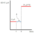
일 실시예에서, 상기 제2 성장 온도는 1500 ℃ ~ 1700 ℃ 범위에서 설정되고, 상기 제1 성장 온도는 1400 ℃ ~ 1500 ℃ 범위에서 설정되며, 상기 제2 성장 속도는 20 ㎛/h 이상의 속도로 설정되고, 상기 제1 성장 속도는 5 ㎛/h 이하의 속도로 설정되며, 상기 제1 두께는 0.5 ㎛ ~ 1.0 ㎛ 범위에서 설정될 수 있다.In one embodiment, the second growth temperature is set in the range of 1500 ° C. to 1700 ° C., the first growth temperature is set in the range of 1400 ° C. to 1500 ° C., and the second growth rate is set to be 20 μm / And the first growth rate is set at a rate of 5 占 퐉 / h or less, and the first thickness may be set in a range of 0.5 占 퐉 to 1.0 占 퐉.
일 실시예에서, 상기 열처리 공정에서의 열처리 온도는 1500 ℃ ~ 1700 ℃ 범위에서 설정될 수 있다.In one embodiment, the heat treatment temperature in the heat treatment process may be set in the range of 1500 ° C to 1700 ° C.
본 발명의 실시예에 의하면, 웨이퍼의 표면 결함 밀도가 감소되며 도핑 균일도가 향상됨으로써, 특성 및 수율이 향상된 고품질의 에피택셜 웨이퍼를 제조할 수 있다.According to the embodiment of the present invention, the surface defect density of the wafer is reduced and the doping uniformity is improved, so that a high-quality epitaxial wafer with improved characteristics and yield can be produced.
도 1은 본 발명의 실시예에 따른 에피택셜 웨이퍼 제조 공정을 설명하기 위한 도면이고,
도 2는 본 발명의 실시예에 따른 에피택셜 웨이퍼 제조 방법을 나타낸 순서도이고,
도 3은 본 발명의 실시예에 따른 에피택셜 웨이퍼 제조 방법에서의 성장 조건을 나타낸 예시 도면이고,
도 4는 본 발명의 실시예에 따른 에피택셜 웨이퍼의 개념도이다.1 is a view for explaining an epitaxial wafer manufacturing process according to an embodiment of the present invention,
2 is a flowchart showing a method of manufacturing an epitaxial wafer according to an embodiment of the present invention,
3 is an exemplary view showing growth conditions in an epitaxial wafer manufacturing method according to an embodiment of the present invention,
4 is a conceptual view of an epitaxial wafer according to an embodiment of the present invention.
본 발명은 다양한 변경을 가할 수 있고 여러 가지 실시예를 가질 수 있는 바, 특정 실시예들을 도면에 예시하고 이를 상세한 설명을 통해 상세히 설명하고자 한다. 그러나, 이는 본 발명을 특정한 실시 형태에 대해 한정하려는 것이 아니며, 본 발명의 사상 및 기술 범위에 포함되는 모든 변경, 균등물 내지 대체물을 포함하는 것으로 이해되어야 한다.While the present invention has been described in connection with certain exemplary embodiments, it is to be understood that the invention is not limited to the disclosed embodiments, but, on the contrary, is intended to cover various modifications and similarities. It should be understood, however, that the invention is not intended to be limited to the particular embodiments, but includes all modifications, equivalents, and alternatives falling within the spirit and scope of the invention.
본 발명을 설명함에 있어서, 관련된 공지 기술에 대한 구체적인 설명이 본 발명의 요지를 불필요하게 흐릴 수 있다고 판단되는 경우 그 상세한 설명을 생략한다. 또한, 본 명세서의 설명 과정에서 이용되는 숫자(예를 들어, 제1, 제2 등)는 하나의 구성요소를 다른 구성요소와 구분하기 위한 식별기호에 불과하다.
DETAILED DESCRIPTION OF THE PREFERRED EMBODIMENTS Hereinafter, the present invention will be described in detail with reference to the accompanying drawings. In addition, numerals (e.g., first, second, etc.) used in the description of the present invention are merely an identifier for distinguishing one component from another.
본 발명은, 제조된 에피택셜 웨이퍼의 표면 결함 밀도(surface defect density)를 감소시킬 수 있는 방법을 제공한다. 이러한 에피택셜 웨이퍼의 표면 결함 밀도는 초기에 투입되는 반응 가스의 양(flux), 성장 온도, 압력, 전체 플럭스(flux), C/Si 비율(ratio), Si/H2 비율 등의 변수들에 의해서 달라질 수 있다. 본 발명에서는 이러한 표면 결함 밀도를 0.5/cm2 이하(즉, 1 cm2 당 0.5개 이하의 결함)로 줄이기 위한 방법을 제공하며, 이를 위해 성장 온도, 성장 속도(즉, 투입되는 반응 가스의 양), 예비 성장될 에피택셜층의 두께, C/Si 비율을 제어하는 방법을 이용한다. 또한 본 발명의 실시예에 따른 에피택셜 웨이퍼 제조 방법에 의하면 도핑 균일도 또한 향상될 수 있다. 이는 이하 첨부된 도면들에 관한 상세한 설명을 통해 명확히 이해될 수 있을 것이다.
The present invention provides a method capable of reducing the surface defect density of epitaxial wafers produced. The density of surface defects of such epitaxial wafers is determined by the variables such as flux, growth temperature, pressure, total flux, C / Si ratio, and Si / H 2 ratio of the initially introduced reaction gas . The present invention provides a method for reducing such surface defect density to 0.5 / cm 2 or less (i.e., 0.5 or less defects per 1 cm 2 ). For this purpose, the growth temperature, growth rate ), The thickness of the epitaxial layer to be preliminarily grown, and the C / Si ratio. In addition, according to the epitaxial wafer manufacturing method according to the embodiment of the present invention, the doping uniformity can also be improved. This can be clearly understood from the following detailed description of the attached drawings.
도 1은 본 발명의 실시예에 따른 에피택셜 웨이퍼 제조 공정을 설명하기 위한 도면이고, 도 2는 본 발명의 실시예에 따른 에피택셜 웨이퍼 제조 방법을 나타낸 순서도이다. 그리고 도 3은 본 발명의 실시예에 따른 에피택셜 웨이퍼 제조 방법에서의 성장 조건을 나타낸 예시 도면이다.FIG. 1 is a view for explaining an epitaxial wafer manufacturing process according to an embodiment of the present invention, and FIG. 2 is a flowchart showing a method of manufacturing an epitaxial wafer according to an embodiment of the present invention. And FIG. 3 is an exemplary view showing growth conditions in an epitaxial wafer manufacturing method according to an embodiment of the present invention.
이하, 도 2의 순서도를 중심으로 도 1 및 도 3을 참조하여 본 발명의 실시예에 따른 에피택셜 웨이퍼 제조 방법에 관하여 상세히 설명한다.Hereinafter, with reference to the flowchart of FIG. 2, a method of manufacturing an epitaxial wafer according to an embodiment of the present invention will be described in detail with reference to FIGS. 1 and 3. FIG.
도 2를 참조하면, 단계 S210에서 반응 챔버 내에 반도체 웨이퍼(도 1의 도면부호 110 참조)를 마련한 후, 본 발명의 실시예에서는 단계 S220과 같은 예비 성장 공정(도 1의 1st 스텝 참조)을 수행한다.Referring to FIG. 2, after a semiconductor wafer (see
도 1을 참조할 때 탄화규소 계열의 웨이퍼(4H-SiC 웨이퍼)가 예시되고 있지만, 위 반도체 웨이퍼는 최종 제작하고자 하는 소자, 제품에 따라 이와 상이할 수 있음은 물론이다. 이와 같은 반도체 웨이퍼 상에 특정 재질의 물질을 적층시키는 공정에 앞서, 그 적층 레이어 간의 격자 상수 불일치 문제로 적층 신뢰성을 담보하기 어려운 경우가 많이 발생한다. 이와 같은 문제의 해결을 위해 위 반도체 웨이퍼 상에 에피택셜층(도 1의 도면부호 115 참조)을 적층(성장)시켜 그 에피택셜층이 일종의 버퍼층으로서의 기능을 수행하도록 하는 방식이 많이 이용된다. 그러나 이러한 에피택셜층의 성장 과정에서, 그 표면에 결함이 발생할 수 있으며, 그 표면 결함이 허용치 이상이 되는 경우(일반적으로 표면 결함 밀도가 1/cm2 를 상회하는 경우)에는 제품의 기판으로서 사용하기에 부적합하다. 따라서 본 발명의 실시예에서는 이러한 표면 결함 밀도를 0.5/cm2 이하로 감소시킬 수 있는 방법으로서 도 2의 단계 S220에서와 같은 예비 성장 공정이라는 단계를 두고 있다.Referring to FIG. 1, a silicon carbide based wafer (4H-SiC wafer) is illustrated, but it goes without saying that the above semiconductor wafer may differ depending on a device and a product to be finally manufactured. Prior to the step of laminating a material of a specific material on such a semiconductor wafer, it is often difficult to secure lamination reliability due to a problem of lattice constant mismatch between the lamination layers. In order to solve such a problem, a method of stacking (growing) an epitaxial layer (see
본 발명의 실시예에 의할 때, 예비 성장 공정은, 단계 S240에 의한 후속 성장 공정에서의 성장 속도(이하, 제2 성장 속도) 보다 저속인 성장 속도(이하, 제1 성장 속도)로 수행된다. 또한 예비 성장 공정은, 단계 S240에 의한 후속 성장 공정에서의 성장 온도(이하, 제2 성장 온도) 보다 저온인 성장 온도(이하, 제1 성장 온도)에서 수행될 수 있다. 예를 들어, 후속 성장 공정에서의 성장 온도가 1500 ℃ ~ 1700 ℃ 범위에서 설정되는 경우, 예비 성장 공정에서의 성장 온도는 1400 ℃ ~ 1500 ℃ 범위에서 설정될 수 있다.According to the embodiment of the present invention, the preliminary growth step is performed at a lower growth rate (hereinafter referred to as a first growth rate) than the growth rate in the subsequent growth step in step S240 (hereinafter, the second growth rate) . Further, the preliminary growth step may be performed at a growth temperature (hereinafter referred to as a first growth temperature) which is lower than the growth temperature (hereinafter, second growth temperature) in the subsequent growth step by step S240. For example, when the growth temperature in the subsequent growth step is set in the range of 1500 占 폚 to 1700 占 폚, the growth temperature in the preliminary growth step may be set in the range of 1400 占 폚 to 1500 占 폚.
즉, 예비 성장 공정은, 반응 챔버 내에 에피택셜 성장을 위한 반응 소스를 주입함에 있어서, 상기 제2 성장 온도 보다 저온인 제1 성장 온도에서 상기 제2 성장 속도 보다 저속인 제1 성장 속도로 상기 반도체 웨이퍼 상에 에피택셜층을 성장시키는 공정에 해당한다. 여기서, 반응 소스는 에피택셜층의 피적층 대상인 반도체 웨이퍼의 재질 및 종류에 따라서 상이해진다. 예를 들어, 도 1과 같이 반도체 웨이퍼(110)가 탄화규소 계열의 웨이퍼인 경우, 이와의 격자 상수 일치가 가능한 물질로서, SiH4+C3H8+H2, MTS(CH3SiCl3), TCS(SiHCl3), SixCx 등의 규소화합물을 함유하는 고상, 액상, 기상의 물질이 상기 반응 소스로서 이용될 수 있을 것이다.That is, in the preliminary growth step, in injecting the reaction source for epitaxial growth into the reaction chamber, the first growth temperature is lower than the second growth temperature, and the first growth rate is lower than the second growth rate, Which corresponds to the step of growing an epitaxial layer on a wafer. Here, the reaction source differs depending on the material and type of the semiconductor wafer to be laminated on the epitaxial layer. For example, when the
이때, 상기 제1 성장 속도는, 예를 들어, 5 ㎛/h 이하의 속도(즉, 시간 당 5 ㎛ 이하의 두께로 에피택셜층이 적층되는 속도)로 설정될 수 있다. 여기서, 성장 속도는 챔버 내에 주입되는 반응 소스의 양(flux)을 조절함으로써 조절 가능하다. At this time, the first growth rate may be set to, for example, a speed of 5 占 퐉 / h or less (i.e., a speed at which the epitaxial layer is laminated to a thickness of 5 占 퐉 or less per hour). Here, the growth rate is adjustable by adjusting the flux of the reaction source injected into the chamber.
일반적으로 에피택셜 성장을 빠른 성장 속도로 수행하는 경우 에피택셜층의 균일한 적층(성장)이 어려울 수 있다. 따라서 위 예비 성장 공정에서는 소정의 성장 온도를 유지함으로써 반응 소스에 의한 원자 간 이동도를 활발히 하여 고른 성장이 가능한 환경을 마련하되, 그 성장 속도는 낮춤으로써 그 원자들이 반도체 웨이퍼 상에 고르게 분포 및 성장될 수 있는 시간을 부여하는 것이다. 따라서 이러한 예비 성장 공정에 의하면 격자 불일치(lattice mismatch)를 줄여 표면 결함을 크게 줄여줄 수 있다. 따라서 이와 같은 예비 성장 공정은 성장 초기의 격자 불일치에 따른 표면 결함을 줄여 후속 성장 공정을 돕기 위한 사전 공정이므로, 예비 성장 공정에 의해 성장되는 에피택셜층의 두께는 대략 0.5 ㎛ ~ 1.0 ㎛ 범위 내이면 충분할 수 있다. 여기서, 예비 성장 공정에 의해 성장될 에피택셜층의 두께는, 위 성장 온도 및 속도와 성장 시간(도 3의 t1 참조)의 조절을 통해 조절 가능하다.In general, when epitaxial growth is performed at a high growth rate, uniform stacking (growth) of the epitaxial layer may be difficult. Therefore, by maintaining the predetermined growth temperature in the preliminary growth step, it is possible to activate the interatomic mobility by the reaction source so as to provide an environment in which uniform growth can be achieved. However, by lowering the growth rate, the atoms are uniformly distributed and grown on the semiconductor wafer It is time to give. Thus, this preliminary growth process can reduce the lattice mismatch and can significantly reduce surface defects. Therefore, since the pre-growth process is a pre-process for reducing the surface defect due to the lattice mismatch at the initial stage of growth to assist the subsequent growth process, the thickness of the epitaxial layer grown by the preliminary growth process is within the range of about 0.5 μm to 1.0 μm It may be enough. Here, the thickness of the epitaxial layer to be grown by the preliminary growth step is adjustable through adjustment of the growth temperature and rate and growth time (see t1 in FIG. 3).
위와 같은 예비 성장 공정을 수행한 이후에는, 단계 S240에서와 같은 후속 성장 공정을 수행하기에 앞서, 단계 S230에서와 같은 열처리 공정(도 1의 Heat treatment 스텝, 도 3의 t1 ~ t2 시간 구간 즉, 도 3의 도면부호 A 참조)을 수행한다. After performing the above-described preliminary growth process, a heat treatment process (the heat treatment process in FIG. 1, a time period from t1 to t2 in FIG. 3, that is, (See A in Fig. 3).
이러한 열처리 공정은 본 발명의 실시예에 따라 제작될 에피택셜 웨이퍼의 도핑 균일도를 향상시키기 위해, 상술한 예비 성장 공정과 후술할 후속 성장 공정 사이에 삽입되는 공정이다. The heat treatment process is inserted between the preliminary growth process described above and the subsequent growth process to be described later in order to improve the doping uniformity of the epitaxial wafer to be manufactured according to the embodiment of the present invention.
일반적으로 에피택셜층을 성장시키는 과정에서 그 성장될 에피택셜층을 N 타입 혹은 P 타입으로 도핑시키는 과정도 동시에 수행하는 경우가 있다. 이러한 도핑은 에피택셜 웨이퍼의 활용 용도, 목적 등에 따라서 정해지며, 위 반응 가스 내에 N 타입 또는 P 타입 도핑에 필요한 도핑 가스를 함께 포함시킴으로써 가능하다. 그러나 특정 극성의 도핑 입자들은 경우에 따라서는 에피택셜층을 구성하는 4족의 원소와 완전히 치환되지 못하고 에피택셜층에 침투만 된 상태로 머무를 수 있다. 따라서 본 발명의 실시예에서는 예비 성장 공정 이후, 후속 성장 공정 이전에 단계 S230에서와 같은 열처리 공정에 따른 단계를 삽입함으로써, 최종 제작된 에피택셜 웨이퍼의 도핑 균일도 또한 향상시키는 방식을 이용하고 있다. In general, a process of doping an epitaxial layer to be grown into an N type or a P type in the process of growing an epitaxial layer may be performed at the same time. Such doping is determined according to the utilization purpose, purpose, etc. of the epitaxial wafer, and it is possible to include doping gas necessary for N type or P type doping in the above reactive gas. However, the doped particles of a specific polarity may remain completely immersed in the epitaxial layer without being completely replaced with the element of Group 4 constituting the epitaxial layer in some cases. Therefore, in the embodiment of the present invention, after the preliminary growth step, a step according to the heat treatment step as in step S230 is inserted before the subsequent growth step, thereby improving the doping uniformity of the finally fabricated epitaxial wafer.
이러한 열처리 공정이 중간에 삽입되면 예비 성장 공정에서 성장된 에피택셜층 내에 단순히 침투된 상태로 머무르던 도핑 입자들이 고온의 열처리 환경에서 4족의 원소와 치환될 수 있는 시간과 에너지가 부여됨으로써, 최종 제작된 에피택셜 웨이퍼의 전체 도핑 균일도를 높일 수 있다.When such a heat treatment process is inserted in the middle, the doping particles which have simply stayed in the epitaxial layer grown in the preliminary growth process are given time and energy to be able to be replaced with the Group 4 element in the high temperature heat treatment environment, It is possible to increase the uniformity of the entire doping of the epitaxial wafer.
상술한 바와 같은 열처리 공정은 소정 시간 동안 진행되며, 이후 단계 S240에 따른 후속 성장 공정이 다시 진행된다. 여기서, 후속 성장 공정은, 앞서 예비 성장 공정에 기반하여 성장된 에피택셜층 위에 본격적으로 에피택셜 성장을 수행하는 공정이며 이미 예비 성장 공정을 거친 후의 성장 공정이므로, 예비 성장 공정에서의 성장 속도에 비해 매우 빠른 속도로 에피택셜 성장을 수행할 수 있다.The above-described heat treatment process is performed for a predetermined time, and then the subsequent growth process according to step S240 is performed again. Here, the subsequent growth step is a step of performing epitaxial growth on the epitaxial layer grown on the basis of the preliminary growth step, and since it is a growth step after the preliminary growth step, The epitaxial growth can be performed at a very high speed.
예를 들어, 단계 S240에 의한 후속 성장 공정은 도 3에 도시된 바와 같이 20 ㎛/h 이상의 속도로 진행될 수 있다. 또한 이러한 후속 성장 공정에서의 성장 온도(즉, 제2 성장 온도)는 앞서 설명한 바와 같이 예를 들어 1500 ℃ ~ 1700 ℃ 범위에서 설정될 수 있다. 그리고 이러한 후속 성장 공정은 에피택셜층의 전체 두께가 성장시키고자 하는 목표 두께가 될 때까지 수행될 수 있다. 이때, 목표 두께는 에피택셜 웨이퍼의 활용 목적, 용도, 최종 소자, 제품의 성격, 설계치 등에 의해 상이해질 수 있다.For example, the subsequent growth process by step S240 may proceed at a speed of 20 [mu] m / h or more as shown in Fig. Also, the growth temperature (i.e., the second growth temperature) in this subsequent growth step may be set, for example, in the range of 1500 ° C to 1700 ° C as described above. And this subsequent growth process can be performed until the total thickness of the epitaxial layer reaches the target thickness to be grown. At this time, the target thickness may be different depending on the purpose of the epitaxial wafer, the application, the final device, the nature of the product, the design value, and the like.
상술한 바와 같이, 성장 속도를 매우 낮춘 상태에서 예비 성장 공정을 먼저 수행한 후 후속 성장 공정을 수행하는 본 발명의 실시예에 따른 에피택셜 웨이퍼 제조 방법에 의하면, 종래 기술에 비해 표면 결함 밀도의 감소는 물론, 공정 시간 및 비용을 크게 줄일 수 있는 이점이 있다.As described above, according to the epitaxial wafer manufacturing method according to the embodiment of the present invention in which the preliminary growth process is performed first and the subsequent growth process is performed in a state in which the growth rate is extremely reduced, the decrease in surface defect density As well as a significant reduction in process time and cost.
종래의 경우, 본 발명의 실시예에서와 같은 예비 성장 공정을 두고 있지 아니하므로, 표면 결함 밀도 문제를 피하기 위해 8~10 ㎛/h 정도의 낮은 성장 속도로 에피택셜층을 성장시켜 왔으며, 이마저도 50 ㎛ 두께로 과도하게 성장시킨 이후 목표 두께까지 다시 제거(polishing)하는 복잡한 과정을 진행하였다. 이와 달리, 본 발명의 실시예에 의하면, 예비 성장 공정 이후에는 표면 결함 밀도의 문제가 제거되므로 이후 후속 성장 공정에서는 매우 빠른 성장 속도로 성장 과정을 진행할 수 있으며, 별도의 폴리싱 공정도 불필요하므로, 전체 공정 시간 및 비용을 획기적으로 줄일 수 있다.
In the prior art, the epitaxial layer has been grown at a low growth rate of about 8 to 10 탆 / h in order to avoid the problem of the surface defect density since the pre-growth process as in the embodiment of the present invention is not performed. And a complicated process of polishing to a target thickness again has been carried out. In contrast, according to the embodiment of the present invention, since the problem of surface defect density is eliminated after the preliminary growth process, the subsequent growth process can proceed at a very high growth rate and no additional polishing process is required. Process time and cost can be drastically reduced.
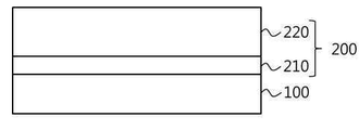
도 4는 본 발명의 실시예에 따른 에피택셜 웨이퍼의 개념도이다.4 is a conceptual view of an epitaxial wafer according to an embodiment of the present invention.
본 발명에 따른 에피택셜 웨이퍼는 기판(100), 및 기판(100)상에 형성된 에피택셜 구조체(200)를 포함한다. 기판(100)은 탄화규소 계열의 웨이퍼일 수 있으며, 이에 대응하여 에피택셜 구조체(200)도 탄화규소 구조체일 수 있다.An epitaxial wafer in accordance with the present invention includes a
구체적으로 에피택셜 구조체(200)는, 기판(100)상에 형성되는 제1에피택셜층(210)과, 제1에피택셜층(210)상에 형성된 제2에피택셜층(220)을 포함한다. Specifically, the
제1에피택셜층(210)은 전술한 예비 성장 공정에 의해 기판(100)상에 형성됨으로써 전압 인가시 누설전류를 잡아주는 역할을 수행한다. 이때, 제1에피택셜층(210)은 1㎛ 이하의 두께를 가질 수 있다.The
제2에피택셜층(220)은 전술한 후속 성장 공정에 의해 목표에 맞는 두께로 제조될 수 있으며, 표면 결함밀도는 0.5cm2이하로 제작될 수 있다.The
이때, 제1에피택셜층(210)과 제2에피택셜층(220)은 모두 n형 전도성 탄화규소계일 수 있다. 즉, 기판(100)이 탄화규소(SiC)인 경우, 제1에피택셜층(210)과 제2에피택셜층(220)은 탄화규소 나이트라이드(SiCN)로 형성될 수 있다. At this time, both the
그러나, 반드시 이에 한정되는 것은 아니고 제1에피택셜층(210)과 제2에피택셜층(220)은 모두 p형 전도성 탄화규소계일 수도 있다. 이 경우 제1에피택셜층(210)과 제2에피택셜층(220)은 알루미늄 탄화규소 (AlSiC)로 형성될 수 있다.However, the
이러한 에피택셜 웨이퍼는 금속 반도체 전계효과 트랜지스터(MESFET)에 적용될 수 있다. 예를 들면, 본 발명에 따른 제2에피택셜층(220)위에 소스 및 드레인을 포함하는 오믹 콘택층을 형성함으로써 금속 반도체 전계 효과 트랜지스터(MESFET)를 제작할 수 있다. 이외에도 다양한 반도체 소자에 적용될 수 있다.
Such an epitaxial wafer can be applied to a metal semiconductor field effect transistor (MESFET). For example, a metal semiconductor field effect transistor (MESFET) can be fabricated by forming an ohmic contact layer including a source and a drain on a
이상에서는 본 발명의 실시예를 참조하여 설명하였지만, 해당 기술 분야에서 통상의 지식을 가진 자라면 하기의 특허 청구의 범위에 기재된 본 발명의 사상 및 영역으로부터 벗어나지 않는 범위 내에서 본 발명을 다양하게 수정 및 변경시킬 수 있음을 쉽게 이해할 수 있을 것이다.While the present invention has been particularly shown and described with reference to exemplary embodiments thereof, it will be understood by those of ordinary skill in the art that various changes in form and details may be made therein without departing from the spirit and scope of the invention as defined by the following claims And changes may be made without departing from the spirit and scope of the invention.
100: 기판 200: 에피택셜 구조체
210: 제1에피택셜층 220: 제2에피택셜층100: substrate 200: epitaxial structure
210: first epitaxial layer 220: second epitaxial layer
Claims (9)
예비 성장된 에피택셜층에 미리 지정된 시간 동안 열처리를 수행하는 열처리 공정; 및
상기 열처리된 반도체 웨이퍼 상에 상기 반응 소스를 주입하여 지정된 제2 성장 온도에서 지정된 제2 성장 속도로 상기 에피택셜층을 목표 두께까지 성장시키는 후속 성장 공정을 포함하고,
상기 제1 성장 속도는 상기 제2 성장 속도 보다 저속인, 에피택셜 웨이퍼의 제조 방법.
Implanting a reaction source for epitaxial growth on a semiconductor wafer provided in the chamber to grow the epitaxial layer at a first predetermined growth rate at a first predetermined growth temperature by a first predetermined thickness;
A heat treatment step of performing a heat treatment on the pre-grown epitaxial layer for a predetermined time; And
And a subsequent growth step of implanting the reaction source onto the heat-treated semiconductor wafer to grow the epitaxial layer to a target thickness at a second growth rate specified at a second growth temperature,
Wherein the first growth rate is lower than the second growth rate.
상기 제1 성장 온도는 상기 제2 성장 온도 보다 저온인, 에피택셜 웨이퍼의 제조 방법.
The method according to claim 1,
Wherein the first growth temperature is lower than the second growth temperature.
상기 반도체 웨이퍼는 탄화규소 웨이퍼이고,
상기 반응 소스는 탄소 및 규소를 포함하는 고상, 액상 또는 기상의 물질인, 에피택셜 웨이퍼의 제조 방법.
The method according to claim 1,
Wherein the semiconductor wafer is a silicon carbide wafer,
Wherein the reaction source is a solid, liquid or gaseous substance including carbon and silicon.
상기 제2 성장 온도는 1500 ℃ ~ 1700 ℃ 범위에서 설정되고, 상기 제1 성장 온도는 1400 ℃ ~ 1500 ℃ 범위에서 설정되며,
상기 제2 성장 속도는 20 ㎛/h 이상의 속도로 설정되고, 상기 제1 성장 속도는 5 ㎛/h 이하의 속도로 설정되며,
상기 제1 두께는 0.5 ㎛ ~ 1 ㎛ 범위에서 설정되는, 에피택셜 웨이퍼의 제조 방법.
The method of claim 3,
The second growth temperature is set in the range of 1500 ° C to 1700 ° C, the first growth temperature is set in the range of 1400 ° C to 1500 ° C,
The second growth rate is set at a rate of 20 占 퐉 / h or more, the first growth rate is set at a rate of 5 占 퐉 / h or less,
Wherein the first thickness is set in the range of 0.5 占 퐉 to 1 占 퐉.
상기 열처리 공정에서의 열처리 온도는 1500 ℃ ~ 1700 ℃ 범위에서 설정되는, 에피택셜 웨이퍼의 제조 방법.
5. The method of claim 4,
Wherein a heat treatment temperature in the heat treatment step is set in a range of 1500 占 폚 to 1700 占 폚.
상기 기판상에 형성된 제1에피택셜층과, 상기 제1에피택셜층상에 형성된 제2에피택셜층을 포함하는 에피택셜 구조체;를 포함하되,
상기 제1에피택셜층과 제2에피택셜층의 조성은 동일한 에피택셜 웨이퍼.
Board; And
An epitaxial structure comprising a first epitaxial layer formed on the substrate and a second epitaxial layer formed on the first epitaxial layer,
Wherein the composition of the first epitaxial layer and the second epitaxial layer is the same.
상기 제2에피택셜층의 표면 결함 밀도는 0.5/cm2이하인 에피택셜 웨이퍼.
The method according to claim 6,
And the surface defect density of the second epitaxial layer is 0.5 / cm < 2 > or less.
상기 기판은 탄화규소 기판이고, 상기 제1에피택셜층과 제2에피택셜층은 탄화규소계로 형성된 에피택셜 웨이퍼.
The method according to claim 6,
Wherein the substrate is a silicon carbide substrate, and the first epitaxial layer and the second epitaxial layer are formed of a silicon carbide based material.
상기 제1에피택셜층의 두께는 1㎛ 이하인 에피택셜 웨이퍼.The method according to claim 6,
Wherein the thickness of the first epitaxial layer is 1 占 퐉 or less.
Priority Applications (4)
| Application Number | Priority Date | Filing Date | Title |
|---|---|---|---|
| KR1020120122007A KR20140055338A (en) | 2012-10-31 | 2012-10-31 | Epitaxial wafer and method for fabricating the same |
| CN201380045238.XA CN104584190B (en) | 2012-10-31 | 2013-10-29 | Epitaxial wafer and its manufacture method |
| PCT/KR2013/009645 WO2014069859A1 (en) | 2012-10-31 | 2013-10-29 | Epitaxial wafer and method for manufacturing same |
| US14/406,070 US9873954B2 (en) | 2012-10-31 | 2013-10-29 | Epitaxial wafer and method for fabricating the same |
Applications Claiming Priority (1)
| Application Number | Priority Date | Filing Date | Title |
|---|---|---|---|
| KR1020120122007A KR20140055338A (en) | 2012-10-31 | 2012-10-31 | Epitaxial wafer and method for fabricating the same |
Publications (1)
| Publication Number | Publication Date |
|---|---|
| KR20140055338A true KR20140055338A (en) | 2014-05-09 |
Family
ID=50627696
Family Applications (1)
| Application Number | Title | Priority Date | Filing Date |
|---|---|---|---|
| KR1020120122007A KR20140055338A (en) | 2012-10-31 | 2012-10-31 | Epitaxial wafer and method for fabricating the same |
Country Status (4)
| Country | Link |
|---|---|
| US (1) | US9873954B2 (en) |
| KR (1) | KR20140055338A (en) |
| CN (1) | CN104584190B (en) |
| WO (1) | WO2014069859A1 (en) |
Cited By (2)
| Publication number | Priority date | Publication date | Assignee | Title |
|---|---|---|---|---|
| KR20180134907A (en) * | 2016-04-20 | 2018-12-19 | 신에쯔 한도타이 가부시키가이샤 | Method for manufacturing an epitaxial wafer |
| KR20190026470A (en) * | 2017-09-05 | 2019-03-13 | 엘지이노텍 주식회사 | Epitaxial wafer and method for fabricating the same |
Families Citing this family (6)
| Publication number | Priority date | Publication date | Assignee | Title |
|---|---|---|---|---|
| US9899489B2 (en) | 2015-02-13 | 2018-02-20 | Taiwan Semiconductor Manufacturing Company, Ltd. | Vertical gate all around (VGAA) devices and methods of manufacturing the same |
| JP6613190B2 (en) * | 2016-03-28 | 2019-11-27 | Kyb株式会社 | Shock absorber |
| CN107829135A (en) * | 2017-10-24 | 2018-03-23 | 瀚天天成电子科技(厦门)有限公司 | A kind of high quality silicon carbide epitaxial growth technique |
| CN113094866B (en) * | 2021-02-25 | 2022-08-26 | 全芯智造技术有限公司 | Simulation method of semiconductor process |
| US11757036B2 (en) * | 2021-07-29 | 2023-09-12 | International Business Machines Corporation | Moon-shaped bottom spacer for vertical transport field effect transistor (VTFET) devices |
| CN114566571B (en) * | 2022-04-24 | 2022-07-26 | 江苏第三代半导体研究院有限公司 | Preparation method of semiconductor epitaxial wafer based on temperature compensation and semiconductor epitaxial wafer |
Family Cites Families (16)
| Publication number | Priority date | Publication date | Assignee | Title |
|---|---|---|---|---|
| US5187547A (en) * | 1988-05-18 | 1993-02-16 | Sanyo Electric Co., Ltd. | Light emitting diode device and method for producing same |
| JP4014676B2 (en) * | 1996-08-13 | 2007-11-28 | 株式会社半導体エネルギー研究所 | Insulated gate type semiconductor device and manufacturing method thereof |
| KR100450781B1 (en) | 1997-08-20 | 2004-11-16 | 삼성전자주식회사 | Method for manufacturing GaN single crystal |
| US6190453B1 (en) * | 1999-07-14 | 2001-02-20 | Seh America, Inc. | Growth of epitaxial semiconductor material with improved crystallographic properties |
| EP1215730B9 (en) * | 1999-09-07 | 2007-08-01 | Sixon Inc. | SiC WAFER, SiC SEMICONDUCTOR DEVICE AND PRODUCTION METHOD OF SiC WAFER |
| DE102006045912B4 (en) * | 2005-09-29 | 2011-07-21 | Sumco Corp. | Method of fabricating a semiconductor device and epitaxial growth device |
| JP2007119273A (en) * | 2005-10-26 | 2007-05-17 | Matsushita Electric Ind Co Ltd | Method for growing silicon carbide single crystal |
| KR20080102065A (en) | 2007-05-18 | 2008-11-24 | 삼성전자주식회사 | Method of forming a epitaxial silicon structure and method of forming a semiconductor device using the same |
| JP5130468B2 (en) | 2007-07-26 | 2013-01-30 | 株式会社エコトロン | Method for manufacturing SiC epitaxial substrate |
| KR100972977B1 (en) * | 2007-12-14 | 2010-07-29 | 삼성엘이디 주식회사 | Growing method of semi-polar nitride single crystal thin film and manufactuing method of nitride semiconductor light emitting devide |
| JP5458509B2 (en) * | 2008-06-04 | 2014-04-02 | 日立金属株式会社 | Silicon carbide semiconductor substrate |
| KR20110116203A (en) * | 2009-03-05 | 2011-10-25 | 미쓰비시덴키 가부시키가이샤 | Method for manufacturing silicon carbide semiconductor device |
| JP2010225733A (en) | 2009-03-23 | 2010-10-07 | Seiko Epson Corp | Method of manufacturing semiconductor substrate |
| TW201037766A (en) * | 2009-04-06 | 2010-10-16 | Univ Nat Chiao Tung | A method of manufacturing III-V group nitride thick film and the structure thereof |
| US8574528B2 (en) * | 2009-09-04 | 2013-11-05 | University Of South Carolina | Methods of growing a silicon carbide epitaxial layer on a substrate to increase and control carrier lifetime |
| CN102534769B (en) * | 2012-03-21 | 2015-01-28 | 中国科学院半导体研究所 | Method for growing gallium nitride epitaxial structure on patterned substrate |
-
2012
- 2012-10-31 KR KR1020120122007A patent/KR20140055338A/en not_active Application Discontinuation
-
2013
- 2013-10-29 US US14/406,070 patent/US9873954B2/en active Active
- 2013-10-29 WO PCT/KR2013/009645 patent/WO2014069859A1/en active Application Filing
- 2013-10-29 CN CN201380045238.XA patent/CN104584190B/en active Active
Cited By (2)
| Publication number | Priority date | Publication date | Assignee | Title |
|---|---|---|---|---|
| KR20180134907A (en) * | 2016-04-20 | 2018-12-19 | 신에쯔 한도타이 가부시키가이샤 | Method for manufacturing an epitaxial wafer |
| KR20190026470A (en) * | 2017-09-05 | 2019-03-13 | 엘지이노텍 주식회사 | Epitaxial wafer and method for fabricating the same |
Also Published As
| Publication number | Publication date |
|---|---|
| CN104584190A (en) | 2015-04-29 |
| WO2014069859A1 (en) | 2014-05-08 |
| US20150259828A1 (en) | 2015-09-17 |
| US9873954B2 (en) | 2018-01-23 |
| CN104584190B (en) | 2017-06-27 |
Similar Documents
| Publication | Publication Date | Title |
|---|---|---|
| KR20140055338A (en) | Epitaxial wafer and method for fabricating the same | |
| EP2728609B1 (en) | Method for fabricating epitaxial wafer | |
| EP2728610B1 (en) | Method for fabricating an epitaxial wafer | |
| KR101971597B1 (en) | Wafer and method of fabrication thin film | |
| US9576793B2 (en) | Semiconductor wafer and method for manufacturing the same | |
| WO2015170500A1 (en) | Sic epitaxial wafer and method for manufacturing silicon carbide semiconductor device | |
| KR20140137795A (en) | Epitaxial wafer | |
| KR20140055337A (en) | Epitaxial wafer and method for fabricating the same | |
| KR20140055336A (en) | Epitaxial wafer and method for fabricating the same | |
| KR20140055335A (en) | Epitaxial wafer and method for fabricating the same | |
| KR102098209B1 (en) | Epitaxial wafer and method for fabricating the same | |
| CN105002563B (en) | The method of silicon carbide epitaxial layers region doping | |
| KR20140070013A (en) | Epitaxial wafer and method for fabricating the same | |
| WO2023058355A1 (en) | Method for forming heteroepitaxial film | |
| JP7259906B2 (en) | Manufacturing method of heteroepitaxial wafer | |
| TW201246288A (en) | Method for producing a III/V SI template | |
| KR102399813B1 (en) | SILICON CARBIDE EPITAXIAl WAFER AND METHOD FOR FABRICATING THE SAME | |
| KR102165615B1 (en) | Epitaxial wafer | |
| KR102339608B1 (en) | Epitaxial wafer and method for fabricating the same | |
| KR102119755B1 (en) | Epitaxial wafer and method for fabricating the same | |
| KR102474331B1 (en) | Epitaxial wafer and method for fabricating the same | |
| KR102131245B1 (en) | Epitaxial wafer | |
| KR20150025648A (en) | Epitaxial wafer | |
| KR102128495B1 (en) | Epitaxial wafer | |
| KR20200075992A (en) | Manufacturing method of silicon carbide epitaxial wafer |
Legal Events
| Date | Code | Title | Description |
|---|---|---|---|
| WITN | Application deemed withdrawn, e.g. because no request for examination was filed or no examination fee was paid |