KR20140053948A - Solid-state imaging element and imaging system - Google Patents
Solid-state imaging element and imaging system Download PDFInfo
- Publication number
- KR20140053948A KR20140053948A KR1020147000593A KR20147000593A KR20140053948A KR 20140053948 A KR20140053948 A KR 20140053948A KR 1020147000593 A KR1020147000593 A KR 1020147000593A KR 20147000593 A KR20147000593 A KR 20147000593A KR 20140053948 A KR20140053948 A KR 20140053948A
- Authority
- KR
- South Korea
- Prior art keywords
- filter
- pixel
- image pickup
- solid
- dimensional
- Prior art date
Links
- 238000003384 imaging method Methods 0.000 title claims abstract description 47
- 238000006243 chemical reaction Methods 0.000 claims abstract description 26
- 230000000737 periodic effect Effects 0.000 claims abstract description 21
- 229910052751 metal Inorganic materials 0.000 claims description 96
- 239000002184 metal Substances 0.000 claims description 96
- 239000010409 thin film Substances 0.000 claims description 89
- 238000000034 method Methods 0.000 claims description 47
- 238000012545 processing Methods 0.000 claims description 30
- 238000001228 spectrum Methods 0.000 claims description 28
- 238000009499 grossing Methods 0.000 claims description 25
- 230000003287 optical effect Effects 0.000 claims description 16
- 238000002834 transmittance Methods 0.000 claims description 13
- 238000004611 spectroscopical analysis Methods 0.000 claims description 8
- 238000003860 storage Methods 0.000 claims description 7
- 239000000463 material Substances 0.000 claims description 5
- 230000007246 mechanism Effects 0.000 claims description 5
- 230000002194 synthesizing effect Effects 0.000 claims description 5
- 238000001914 filtration Methods 0.000 claims description 2
- 230000001360 synchronised effect Effects 0.000 claims description 2
- 238000010030 laminating Methods 0.000 claims 1
- 230000003595 spectral effect Effects 0.000 abstract description 27
- 230000035945 sensitivity Effects 0.000 abstract description 7
- 238000005516 engineering process Methods 0.000 abstract description 5
- 238000013507 mapping Methods 0.000 abstract description 5
- 239000010408 film Substances 0.000 description 35
- 239000010410 layer Substances 0.000 description 33
- 230000006870 function Effects 0.000 description 21
- 238000000701 chemical imaging Methods 0.000 description 18
- 239000004020 conductor Substances 0.000 description 14
- 238000010586 diagram Methods 0.000 description 12
- VYPSYNLAJGMNEJ-UHFFFAOYSA-N Silicium dioxide Chemical compound O=[Si]=O VYPSYNLAJGMNEJ-UHFFFAOYSA-N 0.000 description 10
- 229910052814 silicon oxide Inorganic materials 0.000 description 10
- 239000007789 gas Substances 0.000 description 9
- 229910004298 SiO 2 Inorganic materials 0.000 description 8
- 238000004519 manufacturing process Methods 0.000 description 8
- 239000000758 substrate Substances 0.000 description 8
- 230000005540 biological transmission Effects 0.000 description 7
- 239000011159 matrix material Substances 0.000 description 7
- 238000012546 transfer Methods 0.000 description 6
- 239000000975 dye Substances 0.000 description 5
- 239000011229 interlayer Substances 0.000 description 5
- 238000005268 plasma chemical vapour deposition Methods 0.000 description 5
- 230000000694 effects Effects 0.000 description 4
- 238000005530 etching Methods 0.000 description 4
- ORUIBWPALBXDOA-UHFFFAOYSA-L magnesium fluoride Chemical compound [F-].[F-].[Mg+2] ORUIBWPALBXDOA-UHFFFAOYSA-L 0.000 description 4
- 239000012860 organic pigment Substances 0.000 description 4
- 229910052581 Si3N4 Inorganic materials 0.000 description 3
- 229910052782 aluminium Inorganic materials 0.000 description 3
- 230000015572 biosynthetic process Effects 0.000 description 3
- 238000004364 calculation method Methods 0.000 description 3
- 239000003086 colorant Substances 0.000 description 3
- 230000006866 deterioration Effects 0.000 description 3
- 238000009826 distribution Methods 0.000 description 3
- 230000005571 horizontal transmission Effects 0.000 description 3
- 150000004767 nitrides Chemical class 0.000 description 3
- 230000001681 protective effect Effects 0.000 description 3
- HQVNEWCFYHHQES-UHFFFAOYSA-N silicon nitride Chemical compound N12[Si]34N5[Si]62N3[Si]51N64 HQVNEWCFYHHQES-UHFFFAOYSA-N 0.000 description 3
- 229910052709 silver Inorganic materials 0.000 description 3
- 238000004544 sputter deposition Methods 0.000 description 3
- XPDWGBQVDMORPB-UHFFFAOYSA-N Fluoroform Chemical compound FC(F)F XPDWGBQVDMORPB-UHFFFAOYSA-N 0.000 description 2
- XAGFODPZIPBFFR-UHFFFAOYSA-N aluminium Chemical compound [Al] XAGFODPZIPBFFR-UHFFFAOYSA-N 0.000 description 2
- 230000008901 benefit Effects 0.000 description 2
- 230000008859 change Effects 0.000 description 2
- 239000002131 composite material Substances 0.000 description 2
- 238000000151 deposition Methods 0.000 description 2
- 230000008021 deposition Effects 0.000 description 2
- 238000013461 design Methods 0.000 description 2
- 238000001514 detection method Methods 0.000 description 2
- 238000011161 development Methods 0.000 description 2
- 239000006185 dispersion Substances 0.000 description 2
- 238000000609 electron-beam lithography Methods 0.000 description 2
- 238000011049 filling Methods 0.000 description 2
- 229910052737 gold Inorganic materials 0.000 description 2
- 239000010931 gold Substances 0.000 description 2
- CJNBYAVZURUTKZ-UHFFFAOYSA-N hafnium(iv) oxide Chemical compound O=[Hf]=O CJNBYAVZURUTKZ-UHFFFAOYSA-N 0.000 description 2
- 150000002500 ions Chemical class 0.000 description 2
- 238000005459 micromachining Methods 0.000 description 2
- URLJKFSTXLNXLG-UHFFFAOYSA-N niobium(5+);oxygen(2-) Chemical compound [O-2].[O-2].[O-2].[O-2].[O-2].[Nb+5].[Nb+5] URLJKFSTXLNXLG-UHFFFAOYSA-N 0.000 description 2
- BPUBBGLMJRNUCC-UHFFFAOYSA-N oxygen(2-);tantalum(5+) Chemical compound [O-2].[O-2].[O-2].[O-2].[O-2].[Ta+5].[Ta+5] BPUBBGLMJRNUCC-UHFFFAOYSA-N 0.000 description 2
- RVTZCBVAJQQJTK-UHFFFAOYSA-N oxygen(2-);zirconium(4+) Chemical compound [O-2].[O-2].[Zr+4] RVTZCBVAJQQJTK-UHFFFAOYSA-N 0.000 description 2
- 230000000704 physical effect Effects 0.000 description 2
- 230000004044 response Effects 0.000 description 2
- 239000004065 semiconductor Substances 0.000 description 2
- 229910052710 silicon Inorganic materials 0.000 description 2
- 239000010703 silicon Substances 0.000 description 2
- 238000007514 turning Methods 0.000 description 2
- 229910001928 zirconium oxide Inorganic materials 0.000 description 2
- RYGMFSIKBFXOCR-UHFFFAOYSA-N Copper Chemical group [Cu] RYGMFSIKBFXOCR-UHFFFAOYSA-N 0.000 description 1
- 101001139126 Homo sapiens Krueppel-like factor 6 Proteins 0.000 description 1
- 101000710013 Homo sapiens Reversion-inducing cysteine-rich protein with Kazal motifs Proteins 0.000 description 1
- 238000001069 Raman spectroscopy Methods 0.000 description 1
- 229910018503 SF6 Inorganic materials 0.000 description 1
- BQCADISMDOOEFD-UHFFFAOYSA-N Silver Chemical compound [Ag] BQCADISMDOOEFD-UHFFFAOYSA-N 0.000 description 1
- 229910010413 TiO 2 Inorganic materials 0.000 description 1
- GWEVSGVZZGPLCZ-UHFFFAOYSA-N Titan oxide Chemical compound O=[Ti]=O GWEVSGVZZGPLCZ-UHFFFAOYSA-N 0.000 description 1
- RTAQQCXQSZGOHL-UHFFFAOYSA-N Titanium Chemical compound [Ti] RTAQQCXQSZGOHL-UHFFFAOYSA-N 0.000 description 1
- 238000003491 array Methods 0.000 description 1
- UHYPYGJEEGLRJD-UHFFFAOYSA-N cadmium(2+);selenium(2-) Chemical compound [Se-2].[Cd+2] UHYPYGJEEGLRJD-UHFFFAOYSA-N 0.000 description 1
- 239000011248 coating agent Substances 0.000 description 1
- 238000000576 coating method Methods 0.000 description 1
- 230000000295 complement effect Effects 0.000 description 1
- 230000006835 compression Effects 0.000 description 1
- 238000007906 compression Methods 0.000 description 1
- 239000000470 constituent Substances 0.000 description 1
- 238000010276 construction Methods 0.000 description 1
- 238000007796 conventional method Methods 0.000 description 1
- 238000012937 correction Methods 0.000 description 1
- 239000002537 cosmetic Substances 0.000 description 1
- 239000003989 dielectric material Substances 0.000 description 1
- 238000009792 diffusion process Methods 0.000 description 1
- 238000001312 dry etching Methods 0.000 description 1
- 238000007667 floating Methods 0.000 description 1
- -1 for example Substances 0.000 description 1
- 239000003574 free electron Substances 0.000 description 1
- 239000011521 glass Substances 0.000 description 1
- PCHJSUWPFVWCPO-UHFFFAOYSA-N gold Chemical compound [Au] PCHJSUWPFVWCPO-UHFFFAOYSA-N 0.000 description 1
- 230000036541 health Effects 0.000 description 1
- 238000010438 heat treatment Methods 0.000 description 1
- 238000002513 implantation Methods 0.000 description 1
- 239000012535 impurity Substances 0.000 description 1
- 239000011261 inert gas Substances 0.000 description 1
- 238000007689 inspection Methods 0.000 description 1
- 230000010354 integration Effects 0.000 description 1
- 239000004973 liquid crystal related substance Substances 0.000 description 1
- 238000004518 low pressure chemical vapour deposition Methods 0.000 description 1
- 229910044991 metal oxide Inorganic materials 0.000 description 1
- 150000004706 metal oxides Chemical class 0.000 description 1
- 238000002156 mixing Methods 0.000 description 1
- 239000000203 mixture Substances 0.000 description 1
- 239000011368 organic material Substances 0.000 description 1
- 239000002245 particle Substances 0.000 description 1
- 238000000059 patterning Methods 0.000 description 1
- 238000000206 photolithography Methods 0.000 description 1
- 239000000049 pigment Substances 0.000 description 1
- 229920000642 polymer Polymers 0.000 description 1
- 230000008569 process Effects 0.000 description 1
- 239000002096 quantum dot Substances 0.000 description 1
- 239000000523 sample Substances 0.000 description 1
- 238000000926 separation method Methods 0.000 description 1
- 229910001285 shape-memory alloy Inorganic materials 0.000 description 1
- LIVNPJMFVYWSIS-UHFFFAOYSA-N silicon monoxide Chemical compound [Si-]#[O+] LIVNPJMFVYWSIS-UHFFFAOYSA-N 0.000 description 1
- 239000004332 silver Substances 0.000 description 1
- 229910000679 solder Inorganic materials 0.000 description 1
- 239000007787 solid Substances 0.000 description 1
- 238000000992 sputter etching Methods 0.000 description 1
- SFZCNBIFKDRMGX-UHFFFAOYSA-N sulfur hexafluoride Chemical compound FS(F)(F)(F)(F)F SFZCNBIFKDRMGX-UHFFFAOYSA-N 0.000 description 1
- 229960000909 sulfur hexafluoride Drugs 0.000 description 1
- 239000013077 target material Substances 0.000 description 1
- TXEYQDLBPFQVAA-UHFFFAOYSA-N tetrafluoromethane Chemical compound FC(F)(F)F TXEYQDLBPFQVAA-UHFFFAOYSA-N 0.000 description 1
- 239000010936 titanium Substances 0.000 description 1
- 229910052719 titanium Inorganic materials 0.000 description 1
- ARUUTJKURHLAMI-UHFFFAOYSA-N xenon hexafluoride Chemical compound F[Xe](F)(F)(F)(F)F ARUUTJKURHLAMI-UHFFFAOYSA-N 0.000 description 1
Images


Classifications
-
- H—ELECTRICITY
- H01—ELECTRIC ELEMENTS
- H01L—SEMICONDUCTOR DEVICES NOT COVERED BY CLASS H10
- H01L27/00—Devices consisting of a plurality of semiconductor or other solid-state components formed in or on a common substrate
- H01L27/14—Devices consisting of a plurality of semiconductor or other solid-state components formed in or on a common substrate including semiconductor components sensitive to infrared radiation, light, electromagnetic radiation of shorter wavelength or corpuscular radiation and specially adapted either for the conversion of the energy of such radiation into electrical energy or for the control of electrical energy by such radiation
- H01L27/144—Devices controlled by radiation
- H01L27/146—Imager structures
- H01L27/14601—Structural or functional details thereof
- H01L27/1462—Coatings
- H01L27/14621—Colour filter arrangements
-
- G—PHYSICS
- G01—MEASURING; TESTING
- G01J—MEASUREMENT OF INTENSITY, VELOCITY, SPECTRAL CONTENT, POLARISATION, PHASE OR PULSE CHARACTERISTICS OF INFRARED, VISIBLE OR ULTRAVIOLET LIGHT; COLORIMETRY; RADIATION PYROMETRY
- G01J3/00—Spectrometry; Spectrophotometry; Monochromators; Measuring colours
- G01J3/02—Details
- G01J3/0256—Compact construction
- G01J3/0259—Monolithic
-
- G—PHYSICS
- G01—MEASURING; TESTING
- G01J—MEASUREMENT OF INTENSITY, VELOCITY, SPECTRAL CONTENT, POLARISATION, PHASE OR PULSE CHARACTERISTICS OF INFRARED, VISIBLE OR ULTRAVIOLET LIGHT; COLORIMETRY; RADIATION PYROMETRY
- G01J3/00—Spectrometry; Spectrophotometry; Monochromators; Measuring colours
- G01J3/02—Details
- G01J3/027—Control of working procedures of a spectrometer; Failure detection; Bandwidth calculation
-
- G—PHYSICS
- G01—MEASURING; TESTING
- G01J—MEASUREMENT OF INTENSITY, VELOCITY, SPECTRAL CONTENT, POLARISATION, PHASE OR PULSE CHARACTERISTICS OF INFRARED, VISIBLE OR ULTRAVIOLET LIGHT; COLORIMETRY; RADIATION PYROMETRY
- G01J3/00—Spectrometry; Spectrophotometry; Monochromators; Measuring colours
- G01J3/12—Generating the spectrum; Monochromators
- G01J3/18—Generating the spectrum; Monochromators using diffraction elements, e.g. grating
-
- G—PHYSICS
- G01—MEASURING; TESTING
- G01J—MEASUREMENT OF INTENSITY, VELOCITY, SPECTRAL CONTENT, POLARISATION, PHASE OR PULSE CHARACTERISTICS OF INFRARED, VISIBLE OR ULTRAVIOLET LIGHT; COLORIMETRY; RADIATION PYROMETRY
- G01J3/00—Spectrometry; Spectrophotometry; Monochromators; Measuring colours
- G01J3/28—Investigating the spectrum
- G01J3/2803—Investigating the spectrum using photoelectric array detector
-
- G—PHYSICS
- G01—MEASURING; TESTING
- G01J—MEASUREMENT OF INTENSITY, VELOCITY, SPECTRAL CONTENT, POLARISATION, PHASE OR PULSE CHARACTERISTICS OF INFRARED, VISIBLE OR ULTRAVIOLET LIGHT; COLORIMETRY; RADIATION PYROMETRY
- G01J3/00—Spectrometry; Spectrophotometry; Monochromators; Measuring colours
- G01J3/28—Investigating the spectrum
- G01J3/2823—Imaging spectrometer
-
- G—PHYSICS
- G02—OPTICS
- G02B—OPTICAL ELEMENTS, SYSTEMS OR APPARATUS
- G02B5/00—Optical elements other than lenses
- G02B5/008—Surface plasmon devices
-
- G—PHYSICS
- G02—OPTICS
- G02B—OPTICAL ELEMENTS, SYSTEMS OR APPARATUS
- G02B5/00—Optical elements other than lenses
- G02B5/20—Filters
- G02B5/201—Filters in the form of arrays
-
- H—ELECTRICITY
- H01—ELECTRIC ELEMENTS
- H01L—SEMICONDUCTOR DEVICES NOT COVERED BY CLASS H10
- H01L27/00—Devices consisting of a plurality of semiconductor or other solid-state components formed in or on a common substrate
- H01L27/14—Devices consisting of a plurality of semiconductor or other solid-state components formed in or on a common substrate including semiconductor components sensitive to infrared radiation, light, electromagnetic radiation of shorter wavelength or corpuscular radiation and specially adapted either for the conversion of the energy of such radiation into electrical energy or for the control of electrical energy by such radiation
- H01L27/144—Devices controlled by radiation
- H01L27/146—Imager structures
- H01L27/14601—Structural or functional details thereof
- H01L27/14603—Special geometry or disposition of pixel-elements, address-lines or gate-electrodes
-
- H—ELECTRICITY
- H01—ELECTRIC ELEMENTS
- H01L—SEMICONDUCTOR DEVICES NOT COVERED BY CLASS H10
- H01L27/00—Devices consisting of a plurality of semiconductor or other solid-state components formed in or on a common substrate
- H01L27/14—Devices consisting of a plurality of semiconductor or other solid-state components formed in or on a common substrate including semiconductor components sensitive to infrared radiation, light, electromagnetic radiation of shorter wavelength or corpuscular radiation and specially adapted either for the conversion of the energy of such radiation into electrical energy or for the control of electrical energy by such radiation
- H01L27/144—Devices controlled by radiation
- H01L27/146—Imager structures
- H01L27/14601—Structural or functional details thereof
- H01L27/14625—Optical elements or arrangements associated with the device
- H01L27/14629—Reflectors
-
- H—ELECTRICITY
- H04—ELECTRIC COMMUNICATION TECHNIQUE
- H04N—PICTORIAL COMMUNICATION, e.g. TELEVISION
- H04N23/00—Cameras or camera modules comprising electronic image sensors; Control thereof
- H04N23/10—Cameras or camera modules comprising electronic image sensors; Control thereof for generating image signals from different wavelengths
- H04N23/11—Cameras or camera modules comprising electronic image sensors; Control thereof for generating image signals from different wavelengths for generating image signals from visible and infrared light wavelengths
-
- H—ELECTRICITY
- H04—ELECTRIC COMMUNICATION TECHNIQUE
- H04N—PICTORIAL COMMUNICATION, e.g. TELEVISION
- H04N23/00—Cameras or camera modules comprising electronic image sensors; Control thereof
- H04N23/10—Cameras or camera modules comprising electronic image sensors; Control thereof for generating image signals from different wavelengths
- H04N23/12—Cameras or camera modules comprising electronic image sensors; Control thereof for generating image signals from different wavelengths with one sensor only
-
- H—ELECTRICITY
- H04—ELECTRIC COMMUNICATION TECHNIQUE
- H04N—PICTORIAL COMMUNICATION, e.g. TELEVISION
- H04N25/00—Circuitry of solid-state image sensors [SSIS]; Control thereof
- H04N25/70—SSIS architectures; Circuits associated therewith
- H04N25/71—Charge-coupled device [CCD] sensors; Charge-transfer registers specially adapted for CCD sensors
- H04N25/75—Circuitry for providing, modifying or processing image signals from the pixel array
-
- H—ELECTRICITY
- H04—ELECTRIC COMMUNICATION TECHNIQUE
- H04N—PICTORIAL COMMUNICATION, e.g. TELEVISION
- H04N25/00—Circuitry of solid-state image sensors [SSIS]; Control thereof
- H04N25/70—SSIS architectures; Circuits associated therewith
- H04N25/76—Addressed sensors, e.g. MOS or CMOS sensors
-
- G—PHYSICS
- G01—MEASURING; TESTING
- G01J—MEASUREMENT OF INTENSITY, VELOCITY, SPECTRAL CONTENT, POLARISATION, PHASE OR PULSE CHARACTERISTICS OF INFRARED, VISIBLE OR ULTRAVIOLET LIGHT; COLORIMETRY; RADIATION PYROMETRY
- G01J3/00—Spectrometry; Spectrophotometry; Monochromators; Measuring colours
- G01J3/12—Generating the spectrum; Monochromators
- G01J2003/1213—Filters in general, e.g. dichroic, band
-
- G—PHYSICS
- G01—MEASURING; TESTING
- G01J—MEASUREMENT OF INTENSITY, VELOCITY, SPECTRAL CONTENT, POLARISATION, PHASE OR PULSE CHARACTERISTICS OF INFRARED, VISIBLE OR ULTRAVIOLET LIGHT; COLORIMETRY; RADIATION PYROMETRY
- G01J3/00—Spectrometry; Spectrophotometry; Monochromators; Measuring colours
- G01J3/28—Investigating the spectrum
- G01J3/2803—Investigating the spectrum using photoelectric array detector
- G01J2003/2806—Array and filter array
-
- G—PHYSICS
- G01—MEASURING; TESTING
- G01J—MEASUREMENT OF INTENSITY, VELOCITY, SPECTRAL CONTENT, POLARISATION, PHASE OR PULSE CHARACTERISTICS OF INFRARED, VISIBLE OR ULTRAVIOLET LIGHT; COLORIMETRY; RADIATION PYROMETRY
- G01J3/00—Spectrometry; Spectrophotometry; Monochromators; Measuring colours
- G01J3/28—Investigating the spectrum
- G01J3/2803—Investigating the spectrum using photoelectric array detector
- G01J2003/2816—Semiconductor laminate layer
-
- G—PHYSICS
- G01—MEASURING; TESTING
- G01J—MEASUREMENT OF INTENSITY, VELOCITY, SPECTRAL CONTENT, POLARISATION, PHASE OR PULSE CHARACTERISTICS OF INFRARED, VISIBLE OR ULTRAVIOLET LIGHT; COLORIMETRY; RADIATION PYROMETRY
- G01J3/00—Spectrometry; Spectrophotometry; Monochromators; Measuring colours
- G01J3/28—Investigating the spectrum
- G01J3/2803—Investigating the spectrum using photoelectric array detector
- G01J2003/282—Modified CCD or like
-
- G—PHYSICS
- G01—MEASURING; TESTING
- G01J—MEASUREMENT OF INTENSITY, VELOCITY, SPECTRAL CONTENT, POLARISATION, PHASE OR PULSE CHARACTERISTICS OF INFRARED, VISIBLE OR ULTRAVIOLET LIGHT; COLORIMETRY; RADIATION PYROMETRY
- G01J3/00—Spectrometry; Spectrophotometry; Monochromators; Measuring colours
- G01J3/28—Investigating the spectrum
- G01J3/2823—Imaging spectrometer
- G01J2003/2826—Multispectral imaging, e.g. filter imaging
Abstract
본 기술은, 고감도이면서 높은 파장 분해능을 갖는 가시·근적외선용의 분광·촬상 디바이스를 실현하는 것이 가능하고, 공간 해상도가 높은 2차원 분광 매핑을 가능하게 하는 고체 촬상 소자 및 촬상 시스템을 제공할 수 있는 고체 촬상 소자 및 촬상 시스템에 관한 것이다. 2차원 화소 어레이와, 2차원 화소 어레이의 화소 영역에 대향하도록 배치되고, 검출하여야 할 파장보다도 짧은 주기적인 미세 패턴을 갖는 분광 기능을 구비한 복수종류의 필터를 가지며, 각 필터는, 2차원 화소 어레이의 각 화소의 광전 변환 소자보다도 크고, 인접하는 복수의 광전 변환 소자군에 대해 1종류의 필터가 배치되어 하나의 유닛을 형성하고, 복수종류의 필터는, 인접하는 유닛군에 대해 배치되어 필터 뱅크를 형성하고, 필터 뱅크가 2차원 화소 어레이의 화소 영역에 대향하도록, NxM유닛(단, N, M은 1 이상의 정수) 배치되어 있다.The present technology can realize a solid-state image pickup device and an image pickup system capable of realizing a spectral / imaging device for visible and near-infrared rays having a high sensitivity and a high wavelength resolution and enabling two-dimensional spectral mapping with high spatial resolution State image pickup device and an image pickup system. A plurality of filters having a spectral function having a periodic fine pattern that is shorter than a wavelength to be detected and arranged so as to face the pixel regions of the two-dimensional pixel array, And one type of filter is arranged for a plurality of adjacent photoelectric conversion element groups so that one unit is formed. The plurality of types of filters are arranged for adjacent unit groups, NxM units (where N and M are integers equal to or larger than 1) are arranged so that the bank is formed and the filter bank is opposed to the pixel region of the two-dimensional pixel array.

Description
본 기술은, 검출하여야 할 파장보다 짧은 주기적인 미세 패턴을 갖는 금속 박막 필터를 갖는 고체 촬상 소자 및 촬상 시스템에 관한 것이다.The present technology relates to a solid-state image pickup device and an image pickup system having a metal thin film filter having a periodic fine pattern shorter than a wavelength to be detected.
의료나 미용, 건강 등 다양한 분야에서의 비침습(非侵襲)으로의 검사 용도에 분광 센서가 이용된다.Spectroscopic sensors are used for noninvasive inspection in various fields such as medical, cosmetic, and health.
일반적인 분광 센서는, 가시광 광원이나 적외선 광원 등의 전자파광이나 협대역 파장으로 발광하는 레이저, LED 등을 피사체에 조사하고, 그 반사광이나 라만 산란에 의해 시프트한 광성분을 슬릿을 통과하고 나서 회절 격자에 투과·반사시킨다. 이에 의해, 분광 센서는, 파장 방향의 신호 강도 분포를 공간적인 신호 강도 분포로 변환한다.Conventional spectroscopic sensors irradiate an object with electromagnetic waves such as a visible light source and an infrared light source, a laser that emits light with a narrow wavelength, an LED or the like, pass light components shifted by the reflected light or Raman scattering through the slit, . Thereby, the spectroscopic sensor converts the signal intensity distribution in the wavelength direction into a spatial signal intensity distribution.
그리고, 공간적으로 분리된 각 파장 성분의 전자파 강도를 1차원의 리니어 센서, 또는 2차원 센서로 검출함으로써 입사 스펙트럼의 복원이 가능해진다.The incident spectrum can be restored by detecting the electromagnetic wave intensity of each wavelength component spatially separated by a one-dimensional linear sensor or a two-dimensional sensor.
여기서 검출기로서 이용되는 고체 촬상 소자로서는, CCD(Charge Coupled Device)형이나 CMOS(Complementary Metal Oxide Semiconductor)형의 고체 촬상 소자를 들 수 있다.The solid-state image pickup element used as a detector here may be a CCD (Charge Coupled Device) type or a CMOS (Complementary Metal Oxide Semiconductor) type solid-state image pickup device.
이들 촬상 소자는 일반적인 디지털 카메라나 캠코더, 스마트 폰 등의 휴대 정보 단말용에도 이용되고 있는 촬상 소자와 기본적으로는 동등한 것이고, 일반적인 촬상 용도의 고체 촬상 소자에서는, 그 화소수은 1000만을 초과할 정도로 다화소화하고 있다.These imaging devices are basically equivalent to imaging devices that are also used for portable information terminals such as general digital cameras, camcorders, smart phones, and the like. In general solid-state imaging devices for imaging applications, .
분광 센서에 이용되는 고체 촬상 소자에서도, 통상의 촬상 용도에 이용되는 고체 촬상 소자에서도, 촬상 소자의 각각의 화소는 피사체로부터의 광강도에 응한 신호 전하를 축적하고, 축적한 전하량에 응한 전기 신호를 아날로그 또는 디지털 데이터로서 표본화하여 화상화한다.Even in the solid-state image pickup element used in the spectral sensor and in the solid-state image pickup element used in ordinary image pickup applications, each pixel of the image pickup element accumulates signal charges corresponding to the light intensity from the subject and generates an electric signal corresponding to the accumulated charge amount Sampled and converted into analog or digital data.
그런데 분광 센서·촬상 센서의 여하에 의하지 않고, 고체 촬상 소자는 특정한 전자파 파장대에 감도를 갖는다.However, regardless of the spectral sensor / image sensor, the solid-state image pickup element has sensitivity to a specific electromagnetic wave wavelength band.
예를 들면, 가시 광선·근적외선 대역에서 이용되는 CCD나 CMOS형 고체 촬상 소자의 대부분은 실리콘을 베이스로 제조된다. 실리콘은 그 밴드 갭 때문에 근적외선(내지 1.1㎛)보다도 짧은 파장에 대해서만 감도를 갖는다.For example, most of the CCD and CMOS type solid-state image pickup devices used in the visible light and near-infrared band are made of silicon. Silicon has sensitivity only to wavelengths shorter than near-infrared (~1.1 mu m) due to its bandgap.
그러나, 1.1㎛보다도 단파장의 전자파에 대해서는, 에너지 분해능(파장 분해능)이 없고, 축적된 전하로부터는, 어느 파장의 광을 검출하였는지를 특정할 수가 없다. 그러므로 분광 센서에서는 색·파장마다의 광강도의 정보를 검출 가능하게 하기 위해 회절 격자를 이용하는 경우가 일반적이다.However, for an electromagnetic wave having a shorter wavelength than 1.1 탆, there is no energy resolution (wavelength resolution), and it can not be specified from which accumulated light the light having a wavelength is detected. Therefore, in a spectroscopic sensor, a diffraction grating is generally used to detect information of light intensity for each color and wavelength.
회절 격자에 의해 분광을 하는 경우에 회피할 수 없는 문제로서, 광의 에너지를 파장 방향으로 공간적으로 분리되어 버리는 문제가 있다.There is a problem in that the energy of light is spatially separated in the wavelength direction as a problem that can not be avoided when spectroscopy is performed by the diffraction grating.
결국은 피사체의 토탈의 광을 파장 방향으로 희석하여 검출하기 때문에 높은 파장 분해능(고 분산)을 갖는 분광기를 실현하려면, 그만큼 고체 촬상 소자의 감도를 높이는, 또는 적분 시간을 길게 하여 줄 필요가 있다.Ultimately, in order to realize a spectroscope having a high wavelength resolution (high dispersion) because the total light of a subject is diluted in the wavelength direction and detected, it is necessary to increase the sensitivity of the solid-state image sensor or to increase the integration time.
또한, 입사광은 가는 슬릿을 통과하여 줄 필요가 있기 때문에, 센서에 입사하는 광의 양이 원래 적다는 과제가 있다.Further, since the incident light needs to pass through the thin slit, there is a problem that the amount of light incident on the sensor is originally small.
다른 한편, 일반적인 컬러 촬상 디바이스에서는, 컬러 화상을 취득하기 위해 다음과 같은 수법이 취하여지는 일이 많다.On the other hand, in a general color imaging device, the following technique is often used to acquire a color image.
즉, 2차원 화소 배열의 각 화소에 특정한 파장 성분을 선택적으로 투과하는 수종류의 온 칩 컬러 필터를 구비하고, 인접하는 소수의 화소군에서 복수 파장의 광강도 정보를 취득하여, 디모자이크에 의한 보간 처리에 의해 컬러 화상을 복원하는 수법을 취하는 일이 많다.In other words, it is possible to provide several kinds of on-chip color filters for selectively transmitting a specific wavelength component to each pixel of the two-dimensional pixel array, acquire light intensity information of a plurality of wavelengths from a small number of adjacent pixel groups, A method of restoring a color image by interpolation processing is often taken.
이들 2차원 화소 평면에 복수종류의 필터를 배치하는 수법의 경우, 전술한 회절 격자 및 슬릿 구조와는 달리, 슬릿에서 광을 버릴 필요는 없지만, 역으로 높은 파장 분해능으로 분광하고 싶은 경우에는 큰 과제가 있다.Unlike the above-described diffraction grating and slit structure, in the case of a method of arranging a plurality of kinds of filters on these two-dimensional pixel planes, it is not necessary to discard light from the slit, but when it is desired to perform spectroscopy with high wavelength resolution, .
즉, 필터를 구성하는 염료나 안료 등의 유기 소재는 도포에 의해 형성되기 때문에, 복수종류의 필터를 한번이 실장하는 것은 사실상 불가능하다.That is, since organic materials such as dyes and pigments constituting the filter are formed by coating, it is virtually impossible to mount a plurality of types of filters at once.
즉 RGB 3색으로 컬러 화상을 합성한 통상의 이미징 장치와 비교하여, 10색이나 20색이라는 극단적으로 다색의 필터가 필요해지는 분광 디바이스에서는 비용이 뛰어올라, 실현은 용이하지가 않다.That is, in a spectroscopic device in which an extreme multi-color filter of 10 colors or 20 colors is required as compared with a conventional imaging apparatus in which a color image is synthesized with three colors of R, G, and B, the cost is high, and realization is not easy.
그렇지만 근래, 도체 박막에 검출 파장과 같은 정도 또는 그보다도 미세한 개구를 주기적으로 배치한 홀 어레이 구조, 또는 동(同) 구조와 네가 포지 관계에 있는 아일랜드 어레이 구조는, 플라즈몬 공명체 구조로서 알려져 있다.However, in recent years, a hole array structure in which openings are periodically arranged in the conductor thin film to the same or smaller than the detection wavelength, or an island array structure in which a copper structure and a negative structure are related to each other is known as a plasmon resonance structure.
그리고, 이 플라즈몬 공명체 구조는, 주기나 개구·도트 형상을 최적화함으로써, 투과 파장을 물리 구조로 조정 가능한 필터로서 기능하는 것이 보고되어 있다(비특허 문헌 1, 2 참조).This plasmon resonance structure has been reported to function as a filter capable of adjusting the transmission wavelength to a physical structure by optimizing the period, aperture, and dot shape (see Non-Patent
또한, 이 플라즈몬 공명체를 색 필터로서 이용하는 기술도 개시되어 있다(특허 문헌 1, 2, 3 참조).Further, a technique of using this plasmon resonance body as a color filter is also disclosed (see
이들의 기술은 금속 박막에의 주기 패턴의 패터닝으로 각각의 필터를 실현할 수 있기 때문에, 다종류의 필터를 한번에 실장할 수 있는 장점이 있다.These techniques have an advantage in that various filters can be mounted at one time because each filter can be realized by patterning the periodic pattern on the metal thin film.
그러나, 선행 특허가 개시하는 색 필터 기술을 구비한 고체 촬상 소자에도 과제가 남는다.However, a problem remains in the solid-state image pickup device having the color filter technique disclosed in the prior patent.
플라즈몬 공명체 구조는, 전자파 파장의 λ/2, λ/4 등의 특정 간격의 주기 구조를 반복하여 구비한 구조체에 의해 분광 기능을 발생하는 구조이다. 이 때문에, 파장과 같은 정도의 미세화 화소에 적용하는 데는 부적합하고, 화소 사이즈가 전자파 파장과 비교하여 수배 정도 큰 고체 촬상 소자에만 적용되는 것이 현재의 상태이다.The plasmon resonance structure is a structure that generates a spectroscopic function by a structure in which periodic structures of specific intervals such as? / 2 and? / 4 of the electromagnetic wave wavelength are repeatedly provided. For this reason, it is in the present state that it is not applicable to refinement pixels as much as wavelengths, and is applied only to solid-state image pickup devices whose pixel sizes are several times larger than those of electromagnetic waves.
또한, 높은 파장 분해능의 광신호의 강도 프로파일을 얻는 데는 상당 종류의 필터가 필요해지기 때문에, 공간 해상도가 더욱 크게 저하되는 과제가 남는다. 또한, 상기 각 문헌에는, 고체 촬상 소자의 화소 출력치로부터 입력 스펙트럼을 복원하는 구체적 수단에 관한 기술이 없다.In addition, since a considerable number of filters are required to obtain the intensity profile of the optical signal with high wavelength resolution, the problem that the spatial resolution is further deteriorated remains. Further, in each of the above documents, there is no description on concrete means for restoring the input spectrum from the pixel output value of the solid-state image pickup device.
또한, 출원인은, 금속 박막 필터를 고체 촬상 소자의 화소 영역의 일부에 실장함에 의해, 염가로 분광 기능을 실현하는 수법을 제안하고 있다. 그러나 이 수법에서는, 필터를 실장할 수 있는 화소 영역이 제한되기 때문에, 배치할 수 있는 필터의 수가 적어져 버리는 과제가 있다.The applicant has proposed a technique of realizing a spectroscopic function at low cost by mounting a metal thin film filter in a part of a pixel region of a solid-state image pickup device. However, in this method, there is a problem that the number of filters that can be arranged is reduced because the pixel region in which the filter can be mounted is limited.
그에 의해, 파장 분해능이나 검출하는 신호의 SN의 관점에서 필터를 고체 촬상 소자 전역에 실장하는 경우에 비하여 뒤떨어져 버린다.As a result, the filter is inferior to the case where the filter is mounted over the entire area of the solid-state image pickup element in view of the wavelength resolution and the SN of the signal to be detected.
나아가서는, 미세 가공의 정밀도에는 제한이 있어서, 보다 높은 파장 분해능, 구체적으로는 Δλ=1㎚ 정도의 초고분산 분광을 이 필터 구조만으로 실현하는 데는, 미세 가공의 정밀도에 과제가 있어서, 현시점에서의 실현성은 낮다.Furthermore, there is a limitation in the precision of micro-machining, so that there is a problem in the precision of micromachining in realizing ultra-high dispersion spectroscopy with a higher wavelength resolution, specifically, about ?? = 1 nm with only this filter structure, The feasibility is low.
또한, 1종류의 플라즈몬 공명 필터는 협대역 필터가 아니라 파장마다 복잡한 투과 특성을 나타낸다. 그 때문에, 그들 필터의 투과광 강도로부터 입력 스펙트럼을 추정하려면 어떠한 신호 복원 처리가 필요해진다.In addition, one type of plasmon resonance filter exhibits complex transmission characteristics per wavelength, not narrow band filters. Therefore, any signal restoration processing is required to estimate the input spectrum from the intensity of the transmitted light of those filters.
그러나, 상기한 각 특허 문헌에는 그들의 파형 신호 처리에 관한 수법은 개시되어 있지 않다.However, the above-mentioned respective patent documents do not disclose a technique concerning their waveform signal processing.
본 기술은, 고감도이면서 높은 파장 분해능을 갖는 가시·근적외선용의 분광·촬상 디바이스를 실현하는 것이 가능하고, 공간 해상도가 높은 2차원 분광 매핑을 가능하게 하는 고체 촬상 소자 및 촬상 시스템을 제공하는 것에 있다.It is an object of the present invention to provide a solid-state image pickup device and an image pickup system capable of realizing a spectral / imaging device for visible and near-infrared rays having a high sensitivity and a high wavelength resolution and capable of two-dimensional spectral mapping with high spatial resolution .
본 발명의 제1의 관점의 고체 촬상 소자는, 광전 변환 소자를 포함하는 화소가 어레이형상으로 배열된 2차원 화소 어레이와, 상기 2차원 화소 어레이의 화소 영역에 대향하도록 배치되고, 검출하여야 할 파장보다도 짧은 주기적인 미세 패턴을 갖는 분광 기능을 구비한 복수종류의 필터를 가지며, 상기 각 필터는, 상기 2차원 화소 어레이의 각 화소의 광전 변환 소자보다도 크고, 인접하는 복수의 광전 변환 소자군에 대해 1종류의 필터가 배치된 하나의 유닛을 형성하고, 상기 복수종류의 필터는, 인접하는 유닛군에 대해 배치되어 필터 뱅크를 형성하고, 상기 필터 뱅크가 상기 2차원 화소 어레이의 화소 영역에 대향하도록, NxM유닛(단, N, M은 1 이상의 정수) 배치되어 있다.A solid-state image pickup device according to a first aspect of the present invention is a solid-state image pickup device comprising a two-dimensional pixel array in which pixels including photoelectric conversion elements are arranged in an array, and a plurality of pixels arranged in opposition to pixel regions of the two- And a plurality of filters having a spectroscopic function having a periodic fine pattern that is shorter than a period of the photoelectric conversion elements of the two-dimensional pixel array, wherein each filter is larger than each photoelectric conversion element of each pixel of the two- A plurality of types of filters are disposed for adjacent unit groups to form filter banks, and the filter banks are arranged so as to face the pixel regions of the two-dimensional pixel array , NxM units (where N and M are integers of 1 or more) are arranged.
본 발명의 제2의 관점의 촬상 시스템은, 고체 촬상 소자와, 상기 고체 촬상 소자의 2차원 화소 어레이부에 피사체상을 결상하는 광학계를 가지며, 상기 고체 촬상 소자는, 광전 변환 소자를 포함하는 화소가 어레이형상으로 배열된 2차원 화소 어레이와, 상기 2차원 화소 어레이의 화소 영역에 대향하도록 배치되고, 검출하여야 할 파장보다도 짧은 주기적인 미세 패턴을 갖는 분광 기능을 구비한 복수종류의 필터를 가지며, 상기 각 필터는, 상기 2차원 화소 어레이의 각 화소의 광전 변환 소자보다도 크고, 인접하는 복수의 광전 변환 소자군에 대해 1종류의 필터가 배치된 하나의 유닛을 형성하고, 상기 복수종류의 필터는, 인접하는 유닛군에 대해 배치되어 필터 뱅크를 형성하고, 상기 필터 뱅크가 상기 2차원 화소 어레이의 화소 영역에 대향하도록, NxM유닛(단, N, M은 1 이상의 정수) 배치되어 있다.An image pickup system according to a second aspect of the present invention includes a solid-state image pickup device and an optical system for forming a subject image on a two-dimensional pixel array portion of the solid-state image pickup device, Dimensional array of pixels arranged in an array and a plurality of kinds of filters arranged to face the pixel regions of the two-dimensional pixel array and having a spectroscopic function having a periodic fine pattern shorter than a wavelength to be detected, Wherein each of the filters is larger than a photoelectric conversion element of each pixel of the two-dimensional pixel array and forms one unit in which one kind of filter is disposed for a plurality of adjacent photoelectric conversion element groups, , A filter bank is arranged for the adjacent unit group, and the filter bank is arranged so as to face the pixel region of the two-dimensional pixel array, (Where N and M are integers of 1 or more).
본 발명에 의하면, 고감도이면서 높은 파장 분해능을 갖는 가시·근적외선용의 분광·촬상 디바이스를 실현하는 것이 가능하고, 공간 해상도가 높은 2차원 분광 매핑을 가능하게 한다.According to the present invention, it is possible to realize a spectroscopic / imaging device for visible and near-infrared rays, which has a high sensitivity and a high wavelength resolution, and enables two-dimensional spectral mapping with high spatial resolution.
도 1은 본 실시 형태에 관한 CMOS형 고체 촬상 소자의 구성례를 도시하는 블록도.
도 2는 본 실시 형태에 관한 고체 촬상 소자와 본 금속 박막 필터와의 위치 관계를 설명하기 위한 도면.
도 3은 본 실시 형태에 관한 금속 박막 필터의 구조례를 도시하는 도면.
도 4는 홀 어레이 구조와 네가 포지 반전한 아일랜드 구조의 플라즈몬 공명체 구조체를 도시하는 도면.
도 5는 이면 조사형(BSI) CMOS형 고체 촬상 소자에 관해 본 금속 박막 필터를 배치한 제1의 구조례를 도시하는 도면.
도 6은 이면 조사형(BSI) CMOS형 고체 촬상 소자에 관해 본 금속 박막 필터를 배치한 제2의 구조례를 도시하는 도면.
도 7은 이면 조사형(BSI) CMOS형 고체 촬상 소자에 관해 본 금속 박막 필터를 배치한 제3의 구조례를 도시하는 도면.
도 8은 이면 조사형(BSI) CMOS형 고체 촬상 소자에 관해 본 금속 박막 필터를 배치한 제4의 구조례를 도시하는 도면.
도 9는 이면 조사형(BSI) CMOS형 고체 촬상 소자에 관해 본 금속 박막 필터를 배치한 제5의 구조례를 도시하는 도면.
도 10은 이면 조사형(BSI) CMOS형 고체 촬상 소자에 관해 본 금속 박막 필터를 배치한 제6의 구조례를 도시하는 도면.
도 11은 본 실시 형태의 분광 고체 촬상 소자를 포함하는 분광 촬상 시스템에서 피사체의 전자파 스펙트럼 파형을 유추하는 수법을 개략 설명하기 위한 도면.
도 12는 세로 4유닛, 옆5 유닛의 합계 20유닛의 필터 뱅크로 구성되는 분광 디바이스에서 얻어지는 2차원 분광 맵의 개략도.
도 13은 본 실시 형태에 관한 고체 촬상 소자를 필터 뱅크의 1유닛의 반분의 간격으로 시프트시키면서 각각의 장소에서 색 스펙트럼을 촬영함으로써 공간 해상도를 올리는 수법에 관해 개략 설명하기 위한 도면.
도 14는 본 실시 형태의 분광 촬상 시스템이 유지하는 필터 투과율의 데이터베이스의 교정 방법에 관해 도시하는 플로 차트.
도 15는 본 실시 형태의 분광 촬상 시스템의 구성례를 도시하는 블록도.
도 16은 금속 박막 필터의 제조 장치의 개략 구성을 도시하는 도면.1 is a block diagram showing a configuration example of a CMOS solid-state image pickup device according to the embodiment.
2 is a view for explaining a positional relationship between a solid-state image pickup element and a present metal thin film filter according to the embodiment;
3 is a view showing a configuration example of a metal thin film filter according to the embodiment.
4 is a view showing a plasmon resonance structure having a hole array structure and an inverted inverted structure.
5 is a view showing a first configuration example in which the present metal thin-film filter is arranged for a back-illuminated type (BSI) CMOS type solid-state image pickup device.
6 is a view showing a second configuration example in which the present metal thin-film filter is arranged for a back-illuminated type (BSI) CMOS type solid-state image pickup device.
7 is a view showing a third configuration example in which the present metal thin-film filter is arranged for a back-illuminated type (BSI) CMOS type solid-state image pickup device.
8 is a fourth structural example in which the present metal thin-film filter is disposed on a back-illuminated type (BSI) CMOS type solid-state image pickup device.
9 is a view showing a fifth configuration example in which the present metal thin-film filter is arranged for a back-illuminated type (BSI) CMOS type solid-state image pickup device.
10 is a view showing a sixth configuration example in which the present metal thin-film filter is arranged for a back-illuminated type (BSI) CMOS type solid-state image pickup device.
11 is a view for schematically explaining a method of inferring an electromagnetic spectrum waveform of a subject in a spectral imaging system including the spectral solid-state image pickup device of the present embodiment.
Fig. 12 is a schematic view of a two-dimensional spectral map obtained in a spectroscopic device composed of filter banks of 20 units in total, that is, 4 units vertically and 5 units sideways;
Fig. 13 is a view for schematically explaining a method of increasing spatial resolution by photographing a color spectrum at each place while shifting solid-state image pickup devices according to the present embodiment at half intervals of one unit of a filter bank; Fig.
14 is a flowchart showing a calibration method of a database of the filter transmittance held by the spectral imaging system of the present embodiment.
15 is a block diagram showing a configuration example of the spectral imaging system of the present embodiment.
16 is a view showing a schematic configuration of an apparatus for manufacturing a metal thin film filter;
이하, 본 발명의 실시 형태를 도면에 관련짓어서 설명한다.DESCRIPTION OF THE PREFERRED EMBODIMENTS Hereinafter, embodiments of the present invention will be described with reference to the drawings.
또한, 설명은 이하의 순서로 행한다.The description will be made in the following order.
1. CMOS형 고체 촬상 소자의 전체의 개략 구성례1. Overall configuration example of CMOS type solid-state image pickup device
2. 고체 촬상 소자와 금속 박막 필터와의 위치 관계2. The positional relationship between the solid-state image sensor and the metal thin film filter
3. 금속막 필터의 구성례3. Configuration Example of Metal Film Filter
4. 금속 박막 필터를 배치한 고체 촬상 소자의 구조례4. Structure of solid-state image sensor with metal thin-film filter
5. 피사체의 전자파 스펙트럼 파형을 유추하는 수법5. A method to infer the subject's electromagnetic spectrum waveform
6. 분광 촬상 시스템의 구성례6. Configuration Example of Spectroscopic Imaging System
7. 금속 박막 필터의 제조 방법7. Manufacturing method of metal thin film filter
<1. CMOS형 고체 촬상 소자의 전체의 개략 구성례><1. Overall schematic configuration example of CMOS type solid-state image pickup device>
도 1은, 본 실시 형태에 관한 CMOS형 고체 촬상 소자의 구성례를 도시하는 블록도이다.1 is a block diagram showing a configuration example of a CMOS solid-state image pickup device according to the present embodiment.
이하, 본 기술의 금속 필터를 이면 조사형 CMOS형 고체 촬상 소자에 실장한 예를 나타낸다. 단, 당연하지만 기존의 표면 조사형 CMOS형 고체 촬상 소자라도, CCD형 고체 촬상 소자라도, Si 이외의 예를 들면 CdSe 등의 양자 도트 구조를 광검출부에 이용한 촬상 소자나 유기 광전 소재를 이용한 포토 콘덕터형의 촬상 소자에도 적응이 가능하다.Hereinafter, an example in which the metal filter of the present technology is mounted on a back-illuminated CMOS type solid-state image pickup device is shown. However, it is needless to say that even a conventional surface-irradiation type CMOS type solid-state image pickup element, a CCD type solid-state image pickup element, an image pickup element using a quantum dot structure such as CdSe other than Si, It is possible to adapt to an image pickup device of a turntable type.
이 고체 촬상 소자(100)는, 도 1에 도시하는 바와 같이, 2차원 화소 어레이로서의 화소 어레이부(110), 수직 주사 회로(120), 수평 전송 주사 회로(130), 및 ADC(아날로그-디지털 컨버터)군인 칼럼 ADC 회로(140)를 갖는다.1, this solid-
고체 촬상 소자(100)는, PLL 회로(150), 참조 신호(RAMP)를 생성하는 DAC(디지털-아날로그 컨버터)(160), 및 센스 앰프 회로(S/A)(170)를 갖는다.The solid-state
화소 어레이부(110)는, 포토 다이오드(광전 변환 소자)와 화소 내 앰프를 포함하는 복수의 화소(110A)가 m행n열의 2차원형상(매트릭스형상)으로 배열되어 있다.In the
각 화소(110A)는 광전 변환의 기능을 담당하는 포토 다이오드와 축적된 신호를 판독하기 위한 복수개의 트랜지스터로 구성되는 화소 판독 회로로 이루어진다.Each
도 1에는, 본 실시 형태에 관한 4개의 트랜지스터로 구성되는 CMOS 이미지 센서의 화소의 한 예가 도시되어 있다.Fig. 1 shows an example of a pixel of a CMOS image sensor constituted by four transistors according to the present embodiment.
화소(110A)에서, 포토 다이오드(111)에 축적된 전하는 전송 트랜지스터(112)를 통하여 FD(Floating Diffusion)(113)에 전송된다. FD(113)는 증폭 트랜지스터(114)의 게이트에 접속되어 있다.In the
신호를 판독하고 싶은 화소는, 선택 트랜지스터(115)를 온 함으로써 선택할 수 있다. 선택된 화소의 신호는, 증폭 트랜지스터(114)를 소스 팔로워(SourceFollower) 구동함으로써 축적 전하량에 대응하는 신호로서 신호선(117)에 판독된다. 또한 화소 신호는 리셋 트랜지스터(116)를 온 함으로써 리셋할 수 있다.A pixel to which a signal is to be read can be selected by turning on the
각각의 화소로부터 판독된 신호는 CDS 동작에 의해 신호 레벨이 추출되고, 칼럼 ADC 회로(140), 센스 앰프 회로(170)를 경유하여 디바이스 외부로 출력된다.The signal read from each pixel is extracted by the CDS operation and output to the outside of the device via the
칼럼 ADC 회로(140)는, ADC 블록인 칼럼 처리부(ADC)(141)가 복수열 배열되어 있다.In the
즉, 칼럼 ADC 회로(140)는, k비트 디지털 신호 변환 기능을 가지며, 칼럼 처리부(141)마다 각 수직 신호선(열선)(117)마다 배치되고, 열병렬 ADC 블록이 구성된다.That is, the
각 칼럼 처리부(141)는, DAC(160)에 의해 생성되는 참조 신호를 계단형상으로 변화시킨 램프파형인 참조 신호(RAMP)와, 행선(行線)마다 화소로부터 수직 신호선을 경유하여 얻어지는 아날로그 신호(VSL)를 비교하는 비교기(비교 회로)(141-1)를 갖는다.Each
또한, 각 칼럼 처리부(141)는, 비교 시간을 카운트하고, 카운트 결과를 유지하는 카운터 래치(카운터)(141-2)를 갖는다.Each
각 카운터(141-2)의 출력은, 예를 들면 k비트폭의 수평 전송선(LTRF)에 접속되어 있다.The output of each counter 141-2 is connected to a horizontal transmission line LTRF having a width of, for example, k bits.
그리고, 수평 전송선(LTRF)에 대응하는 센스 앰프 회로(170)가 배치된다.A
칼럼 ADC 회로(140)에서는, 수직 신호선(117)에 판독된 아날로그 신호 전위(VSL)는 열마다(칼럼마다) 배치된 비교기(141-1)에서 참조 신호(RAMP)와 비교된다.In the
이때, 비교기(141-1)와 마찬가지로 열마다 배치된 카운터(141-2)가 동작하고 있다.At this time, as in the case of the comparator 141-1, the counter 141-2 arranged for each column operates.
각 칼럼 처리부(141)는, 램프 파형의 어느 참조 신호(RAMP)와 카운터 값이 1대1의 대응을 취하면서 변화함으로써 수직 신호선(117)의 전위(아날로그 신호)(VSL)를 디지털 신호로 변환한다.Each
칼럼 처리부(ADC)(141)는, 참조 신호(RAMP)(전위(VSLop))의 전압의 변화를 시간의 변화로 변환하는 것이고, 그 시간을 어느 주기(클록)로 셈으로써 디지털값으로 변환한다.The column processing unit (ADC) 141 converts a change in the voltage of the reference signal RAMP (potential (VSLop)) into a change in time and converts the time into a digital value by multiplying the time by a certain period (clock) .
아날로그 신호(VSL와 참조 신호(RAMP)(Vslop)가 교차한 때, 비교기(141-1)의 출력이 반전하고, 카운터(141-2)의 입력 클록을 정지하고, 또는, 입력을 정지하고 있던 클록을 카운터(141-2)에 입력하여, AD 변환을 완료시킨다.When the analog signal VSL crosses the reference signal RAMP (Vslop), the output of the comparator 141-1 is inverted, the input clock of the counter 141-2 is stopped, or the input The clock is input to the counter 141-2 to complete the AD conversion.
이상의 AD 변환기간 종료 후, 수평 전송 주사 회로(130)에 의해, 카운터(141-2)에서 유지된 데이터가, 수평 전송선(LTRF)에 전송되고, 센스 앰프 회로(170)를 경유하여 외부의 신호 처리 회로에 출력되고, 소정의 신호 처리에 의해 2차원 화상이 생성된다.The data held in the counter 141-2 is transferred to the horizontal transfer line LTRF by the horizontal
외부에 출력된 화소치 데이터는 각각의 화소 위치에서는 단독의 필터에 대응하는 강도 정보밖에 갖지 않기 때문에, 인접하는 이색(異色) 화소의 강도 정보로부터, 각각의 화소 위치에서의 각각의 색성분의 강도 정보를 디모자이크 처리나 콘벌루션 처리 등의 보간에 의해 복원된다.Since the pixel value data output to the outside has only intensity information corresponding to a single filter at each pixel position, intensity information of each color component at each pixel position is obtained from intensity information of adjacent two different color pixels Is restored by interpolation such as demosaicing or convolution processing.
그 밖에, 화이트 밸런스나 감마 보정, 윤곽 강조, 화상 압축 등의 처리가 행하여저서, 관측자에게 있어서 바람직한, 또는 피사체에 충실한 화상이 복원된다.In addition, processing such as white balance, gamma correction, contour enhancement, image compression, and the like are performed to restore an image that is desirable for an observer or faithful to a subject.
또한, 칩에 화상 처리 프로세서가 실장된 시스템 온 칩형의 이미지 센서의 경우는, 이들의 신호 처리도 동일 칩상에서 행할 수가 있어서, 생(生)화상 데이터 외에 jpeg나 mpeg 방식 등의 압축 화상을 출력하는 경우도 있다.Further, in the case of a system-on-chip type image sensor in which an image processing processor is mounted on a chip, these signal processing can also be performed on the same chip, and a compressed image such as a jpeg or mpeg method other than raw image data is output There are also cases.
<2. 고체 촬상 소자와 금속 박막 필터와의 위치 관계><2. Solid-state image pickup device and metal thin film filter>
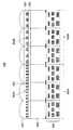
도 2는, 본 실시 형태에 관한 고체 촬상 소자와 본 금속 박막 필터와의 위치 관계를 설명하기 위한 도면이다.2 is a diagram for explaining the positional relationship between the solid-state image pickup device and the present thin metal film filter according to the embodiment.
도 2에서, 도 1의 화소 어레이부(110)가 2차원 화소군(201)으로서 나타나 있다.In Fig. 2, the
2차원 화소군(201)은, 예를 들면 세로·가로 각각 수천개의 화소(PXL)에 의해 형성되고, 적은 디바이스라도 100만화소 정도, 많은 것에서는 수천만화소에도 미치는 거대한 2차원 화소군을 구성한다.The two-
본 실시 형태의 금속 박막 필터군(필터 뱅크)(202)은, 2차원 화소군(화소 어레이부)(201)의 광입사면에 대향하도록 배치된다.The metal thin film filter group (filter bank) 202 of the present embodiment is disposed so as to face the light incident surface of the two-dimensional pixel group (pixel array unit)
여기서, 각 필터(MFL)는 필터 뱅크(202)의 하나의 사각형에 대응한다. 각 필터(202FL)의 사이즈는 광검출 화소(PXL)에 대해 가로(X축)방향으로 U화소, 세로(Y축)방향으로 V화소의 화소 영역에 대해 1종류가 실장된다.Here, each filter MFL corresponds to one square of the
즉 인접하는 U*V화소에 대해 1종류의 필터(MFL)가 실장된다.That is, one kind of filter (MFL) is mounted for adjacent U * V pixels.
또한, 필터(MFL)는, 가로(X축)방향으로 K종류, 세로(Y축)방향으로 L종류로 1개의 유닛(필터 뱅크)(202)을 구성한다.The filter MFL constitutes one unit (filter bank) 202 in L types in K (longitudinal) and Y (longitudinal) directions in the horizontal (X axis) direction.
도 2의 예에서는, K=5, L=4의 20종류로 1개의 필터 뱅크를 구성하는 예로 되어 있다.In the example of FIG. 2, 20 types of K = 5 and L = 4 constitute one filter bank.
또한, 필터 뱅크(202)는 2차원 촬상 소자 전면(全面)에 가로(X축)방향으로 N유닛, 세로(Y축)방향으로 M유닛 배치되고, N*M종류의 필터 뱅크 어레이(203)에 의해 구성된다.The
즉, 도 2의 예의 필터 뱅크(202)는, K=5, L=4의 20종류의 필터를 가지며, 그것이, N=4, M=4, 합계 16유닛 있는 것이 된다.That is, the
또한, 필터 뱅크(202), 또는 필터 뱅크군의 분광 기능 블록인 금속 박막 필터는 층간 절연막에 끼어져 있고, 그 절연막은 복수종류의 굴절률이라도 상관없다.The
예를 들면, 필터 뱅크 어레이(203) 중, 도 2의 A라인은 굴절률=1.42이고, B라인은 굴절률=1.40, C라인에서는 굴절률=1.38, D라인에서는 굴절률=1.36 등과 같이 설정 가능하다.For example, in the
즉, 2차원 촬상 소자 영역의 화소 영역마다 다른 굴절률을 갖도록 할 수 있다.That is, it is possible to have a different refractive index for each pixel region of the two-dimensional imaging element region.
여기서, SiO2의 굴절률의 컨트롤은, 예를 들면 플라즈마 CVD법에 의해 SiO2막을 성막할 때, CF4 가스의 유량을 컨트롤함으로써 굴절률의 조정을 할 수 있다.Here, control of the refractive index of SiO 2, for example, when the SiO 2 film deposition by plasma CVD, it is possible to adjust the refractive index by controlling the flow rate of CF 4 gas.
<3. 금속막 필터의 구성례><3. Configuration Example of Metal Film Filter>
도 3의 (A) 내지 (D)는, 본 실시 형태에 관한 금속 박막 필터의 구조례를 도시하는 도면이다.3 (A) to 3 (D) are diagrams showing the construction of a metal thin film filter according to the present embodiment.
도 3에서는, 금속막 필터를 부호 300으로 나타내고 있다.3, the metal film filter 300 is shown.
도 3의 (A)는 허니컴 배열(301)을, 도 3의 (B)는 직교 행렬 배열(302)을, 도 3의 (C)는 관통 개구와 비관통 개구가 혼재한 배열(303)을, 도 3의 (D)는 도 3의 (C)의 A-A'선의 단면으로서 오목구조를 갖는 비관통 구멍을 포함하는 배열(304)을 각각 도시하고 있다.3 (A) shows a
금속 박막 필터(300)는, 그 미세 구조 패턴에 의해 특정한 전자파 파장에서 자유 전자와 광이 커플링한 표면 플라즈몬-폴라리톤이 생긴다.In the metal thin film filter 300, a surface plasmon-polariton is generated in which free electrons and light are coupled at a specific electromagnetic wave wavelength by the fine structure pattern.
이 금속 박막 필터(300)는, 자외선 파장대에 플라즈마 주파수를 갖는 도체 소재(구체적으로는 은이나 알루미늄, 금 등이 알맞다)로 이루어지는 박막에 미세 가공을 시행한 서브 파장 구조체이다.The metal thin film filter 300 is a sub-wavelength structure in which a thin film made of a conductor material having a plasma frequency at an ultraviolet wavelength band (specifically, silver, aluminum, gold or the like is suitable) is microfabricated.
그리고, 금속 박막 필터(300)는, 도체의 물성과 패턴 주기·개구경(開口徑)·도트 사이즈·막두께·구조체의 주위의 매질의 물성에 의해 정해지는 공명 파장을 갖는다.The metal thin film filter 300 has a resonance wavelength determined by physical properties of a conductor and physical properties of a pattern period, an opening diameter, a dot size, a film thickness, and a medium around the structure.
기본 구조는 홀 어레이 구조이고, 검출 파장보다도 작은 지름을 갖는 개구(홀)(Hl)를 2차원 배열형상으로 배치한다.The basic structure is a hole array structure, and openings (holes) H1 having a diameter smaller than the detection wavelength are arranged in a two-dimensional arrangement.
홀 배치는 도 3의 (A)에 도시하는 바와 같은 허니컴 배열(301), 또는 도 3의 (B)에 도시하는 바와 같은 직교 행렬 배열(302)로 배치하는 것이 알맞지만, 그 밖의 배열이라도 주기성이 있는 구조라면 상관없다.It is appropriate to arrange the holes in the
여기서, 홀 간격이나 홀 사이즈·막두께가 투과 특성의 키 파라미터가 된다. 도 3에서는, 홀 개구부는 305, 도체부분은 306으로 나타내고 있다.Here, the hole interval, hole size, and film thickness are key parameters of the transmission characteristic. In Fig. 3, the hole opening is denoted by 305 and the conductor portion is denoted by 306. [
홀 개구(305)의 개구경은 투과시키고 싶은 파장보다도 작고, 직경 100[㎚] 정도가 알맞다. 설계 자유도가 있기 때문에, 대강 50[㎚] 내지 200[㎚]의 범위라면 상관없다.The opening diameter of the
또한, 도체 박막(306)의 두께는 100[㎚] 정도가 알맞지만, 10[㎚] 내지 200[㎚] 정도의 범위라면 상관없다.Though the thickness of the conductor
또한, 인접 홀 사이와의 간격(307, 308)을 조정함으로써, 투과 파장을 변화시킬 수 있지만, 매질 중에서의 실효적인 전자파 파장의 반파장 내지 1파장 정도의 범위가 알맞고, 구체적으로는 150[㎚] 내지 1000[㎚] 정도의 홀 간격이 바람직하다.Though the transmission wavelength can be changed by adjusting the
또한, 홀 어레이 구조의 모든 개구가 도체 박막을 관통하고 있을 필요는 없고, 도 3의 (C) 및 (B)의 배열(303, 304)에 도시하는 바와 같이, 일부, 또는 모든 개구는 도체상에 오목구조를 갖는 비관통 구멍이라도 상관없다.It is not necessary that all the openings of the hole array structure pass through the conductor thin film, and as shown in the
도 3의 (C) 및 (D)는, 관통 개구(305)와 비관통 개구(309)가 주기적으로 배치한 경우의 실시례이다.3C and 3D show an embodiment in which the through-
또한, 홀 개구의 형상은 가공상(上), 원형이 바람직하지만 타원형상이나 다각형 형상, 성형, 십자형, 링 형, 만형(卍形) 등이라도 상관없다.Further, the shape of the hole opening is preferably a circular shape, but it may be an elliptical shape, a polygonal shape, a molded shape, a cruciform shape, a ring shape, a manjak shape, or the like.
도 4의 (A) 및 (B)는, 홀 어레이 구조와 네가 포지 반전한 아일랜드 구조의 플라즈몬 공명체 구조체를 도시하는 도면이다.Figs. 4A and 4B are diagrams showing a plasmon resonance structure having a hole array structure and an inverted inverted structure. Fig.
아일랜드 배치(400)는, 도 4의 (A)에 도시하는바 같은 허니컴 배열(401), 도 4의 (B)에 도시하는 바와 같은 직교 행렬 배열(402)이 알맞다.As the island arrangement 400, a
각 아일랜드(403)는 20 내지 200[㎚]의 사이즈를 가지며, 아일랜드 간부(間部)(404)는 실리콘 산화막 등의 유전체 소재로 충전된다.Each
인접 아일랜드 사이의 기본 간격(405, 406)은, 매질 중에서의 실행적(實行的)인 전자파 파장의 반파장이 알맞고, 설계 자유도를 가미하면 1/4파장 내지 1파장의 범위가 알맞다. 또한 아일랜드 구조의 형상은, 가공상은 원형이 바람직하지만 타원형상이나 다각형 형상, 성형, 십자형, 링 형, 만형 등이라도 상관없다.The
<4. 금속 박막 필터를 배치한 고체 촬상 소자의 구조례><4. Solid-state image pickup device in which a metal thin film filter is arranged>
도 5는, 이면 조사형(BSI) CMOS형 고체 촬상 소자에 관해 본 금속 박막 필터를 배치한 제1의 구조례를 도시하는 도면이다.Fig. 5 is a diagram showing a first configuration example in which the present thin metal film filter is arranged for a back-illuminated type (BSI) CMOS type solid-state image pickup device.
도 5는, 2차원 고체 촬상 소자 어레이를 구성하는 화소군중, 인접하는 6화소분을 잘라내어 단면 모식도로서 기재하고 있다. 당연하지만 실제로는 이들의 화소가 2차원 평면에 화소수만큼 전개된다.5 is a schematic cross-sectional view of a pixel group constituting a two-dimensional solid-state imaging element array, in which six adjacent pixels are cut out. However, actually, these pixels are developed in the two-dimensional plane by the number of pixels.
도 5의 고체 촬상 소자(500)에서, 501은 온 칩 마이크로 렌즈를, 502A, 502B는 금속 박막 필터를, 503은 평활화층을, 504는 포토 다이오드를, 505는 신호 배선층을, 506A, 506B는 인접 화소를, 각각 나타내고 있다.5,
온 칩 마이크로 렌즈(501)는, 포토 다이오드(504)에 효율적으로 광을 유도하기 위한 광학 소자이다.The on-
포토 다이오드(504)는, P형 영역에 둘러싸인 N형 영역, 또는 N형 영역에 둘러싸인 P형 영역이고, 주위보다도 전위가 깊은 영역에 광전 변환에 의해 생긴 전자·홀을 신호 전하로서 축적하는 기능을 갖는다.The
금속 박막 필터(502A, 502B)는, 예를 들면 Al이나 Ag에 의해 형성되는 금속 박막 필터에 서브 파장 간격으로 주기적인 구조를 패터닝한 구조체이다(도 3, 도 4).The metal
금속 박막 필터(502A, 502B)는, 포토 다이오드(504) 상방에 실리콘 산화막·질화막 등으로 이루어지는 평활화층(503)을 형성하고, 그 위에 실장되는 것이 바람직하다. 또한, 금속 박막 필터(502A, 502B)를 보호하는 층간 절연막·보호막(평활화층)(507)은 실리콘 산화막(SiO2) 및 SiO2를 주성분으로 하는 복합 소재가 알맞다. 그 밖에 불화마그네슘(MgF2)이나 중공 구조(Air Gap) 등을 저굴절률의 매질로서 이용할 수도 있다.It is preferable that the metal
여기서 도체 박막 필터(502A, 502B)는, 인접하는 화소 사이에서 공통의 패턴 구조인 것이 바람직하다. 예를 들면, 도 5에서는 인접 3화소(506A)가 금속 박막 필터(502A)를 실장하고, 다른 3화소(506B)가 금속 박막 필터(502B)를 실장하고 있다.Here, it is preferable that the conductor
당연하지만, 필터의 종류는 2종류로 한정되지 않고, 또한 동일 필터를 공유한 화소수도 3화소로는 한정되지 않고, 임의의 정수(예를 들면 인접 8화소 공유, 64화소 공유, 128화소 공유 등)로 공유할 수 있다.Of course, the types of filters are not limited to two types, and the number of pixels sharing the same filter is not limited to three pixels but may be any integer (for example, adjacent 8-pixel sharing, 64-pixel sharing, ).
신호 배선층(505)은, 광전 변환에 의해 포토 다이오드(504)에 축적된 신호 전하를 외부에 판독하기 위한 신호 배선층으로서 형성되어 있다.The
포토 다이오드(504)는, 인접하는 포토 다이오드와 전기적으로 분리하기 위해, STI 등의 산화막 분리에 의해 소자 분리되는 외에, 불순물의 임플랜테이션에 의한 EDI 구조나 CION 구조 등에 의해 전기적으로 분리되어 있다.The
도 6은, 이면 조사형(BSI) CMOS형 고체 촬상 소자에 관해 본 금속 박막 필터를 배치한 제2의 구조례를 도시하는 도면이다.Fig. 6 is a diagram showing a second configuration example in which the present metal thin-film filter is arranged for a back-illuminated type (BSI) CMOS type solid-state image pickup device.
도 6에서, 도 5와 동일 구성 부분은, 이해를 용이하게 하기 위해 동일 부호로써 나타내고 있다.In Fig. 6, the same constituent parts as those in Fig. 5 are denoted by the same reference numerals for ease of understanding.
도 6의 CMOS형 고체 촬상 소자(500A)가 도 5의 CMOS형 고체 촬상 소자(500와 다른 점은, 이하와 같다.The CMOS type solid-state
이 CMOS형 고체 촬상 소자(500A)는, 온 칩 마이크로 렌즈(501)의 상층에는 SiO2나 불화마그네슘(MgF2) 등으로 형성되는 저굴절률 소재로 이루어지는 저굴절률 평활화층(507A)을 갖는다. 여기서 온 칩 마이크로 렌즈(501)의 굴절률은 평활화층(507A)의 굴절률보다 높을 필요가 있다.This CMOS type solid-
상술한 바와 같이, 금속 박막 필터(502A, 502B)는, 포토 다이오드(504) 상방에 실리콘 산화막·질화막 등으로 이루어지는 평활화층(503)을 형성하고, 그 위에 실장되는 것이 바람직하다.As described above, it is preferable that the metal
도 6의 예에서는, 저굴절률 평활화층(507A)의 상층에 평활화층(503)이 형성되고, 평활화층(503)상에 금속 박막 필터(502A, 502B)가 형성되어 있다.6, a
상술한 바와 같이, 필터(502A, 502B)는, 도체 박막 필터(플라즈몬 공명체)(502)에 의해 형성되고, 예를 들면 Al나 Ag에 의해 형성되는 금속 박막 필터(도 3, 도 4)에 서브 파장 간격으로 주기적인 구조를 패터닝한 구조체이다.As described above, the
또한 일반적인 고체 촬상 소자에서는, 온 칩 마이크로 렌즈(501)의 하류(하층)에 RGB 등의 컬러 필터가 실장되어 있는 경우가 많고, 도 6의 예에서도, 유기 안료·염료로 이루어지는 일반적인 컬러 필터(508)를 배치할 수도 있다In a typical solid-state image pickup device, a color filter such as RGB is mounted on the downstream (lower layer) of the on-
그에 의해, 기존의 필터(508)와 금속 박막 필터(602A, 602B)와의 조합의 자유도가 높아지고, 보다 높은 파장 분해능으로 파장 스펙트럼을 얻는 것이 가능해진다.Thereby, the degree of freedom in combination of the
도 7은, 이면 조사형(BSI) CMOS형 고체 촬상 소자에 관해 본 금속 박막 필터를 배치한 제3의 구조례를 도시하는 도면이다.Fig. 7 is a diagram showing a third configuration example in which the present metal thin-film filter is arranged for a back-illuminated type (BSI) CMOS type solid-state image pickup device.
도 7에서, 도 5 및 도 6과 동일 구성 부분은, 이해를 용이하게 하기 위해 동일 부호로써 나타내고 있다.In Fig. 7, the same components as those in Figs. 5 and 6 are denoted by the same reference numerals for ease of understanding.
도 7의 CMOS형 고체 촬상 소자(500B)가 도 6의 CMOS형 고체 촬상 소자(500A)와 다른 점은, 이하와 같다.The CMOS type solid-state
이 CMOS형 고체 촬상 소자(500B)에서는, 2화소(506A)가 금속 박막 필터(502A)를 실장하고, 다른 2화소(506C)가 금속 박막 필터(502C)를 실장한 예로 되어 있다.In the CMOS type solid-
2화소(506A)와 2화소(506C)의 사이의 화소(506B)에는 화소 전면을 차광하는 금속 박막 필터(502B)가 실장되어 있다.A metal
본 구성에 의해 금속 박막 필터(502A)를 투과한 광이 다른 금속 박막 필터(502C)를 구비한 화소(506C)에 혼입되는 혼색 성분은 대폭적으로 저감이 가능하고, 혼색에 의한 화질 열화나 파장 스펙트럼의 열화의 문제를 경감할 수 있다.With this configuration, the color mixture component in which the light transmitted through the metal
상술한 바와 같이, 필터(502A, 502B, 502C)는, 도체 박막 필터(플라즈몬 공명체)(502)에 의해 형성되고, 예를 들면 Al나 Ag에 의해 형성되는 금속 박막 필터(도 3, 도 4)에 서브 파장 간격으로 주기적인 구조를 패터닝한 구조체이다.As described above, the
또한, 도 7의 예에서도, 유기 안료·염료로 이루어지는 일반적인 컬러 필터(508)를 배치할 수도 있다.Also in the example of Fig. 7, a
도 8은, 이면 조사형(BSI) CMOS형 고체 촬상 소자에 관해 본 금속 박막 필터를 배치한 제4의 구조례를 도시하는 도면이다.Fig. 8 is a diagram showing a fourth configuration example in which the present thin metal film filter is arranged for a back-illuminated type (BSI) CMOS type solid-state image pickup device.
도 8에서, 도 5 내지 도 7과 동일 구성 부분은, 이해를 용이하게 하기 위해 동일 부호로써 나타내고 있다.In Fig. 8, the same components as those in Figs. 5 to 7 are denoted by the same reference numerals in order to facilitate understanding.
도 8의 CMOS형 고체 촬상 소자(500C)가 도 6의 CMOS형 고체 촬상 소자(500A)와 다른 점은, 이하와 같다.The CMOS type solid-state
이 CMOS형 고체 촬상 소자(500C)에서는, 금속 박막 필터(502A, 502B)는 SiO, SiN 등의 유전체에 의해 형성되는 보호막으로서의 평활화층(503)에 의해 주위가 충전된 구조로 되어 있다.In the CMOS type solid-state
도 8의 고체 촬상 소자(500C)는, 3화소(506A)가 금속 박막 필터(502A)를 실장하고, 다른 3화소(506B)가 금속 박막 필터(502B)를 실장한 예이다.8 is an example in which the three
당연하지만, 금속 박막 필터의 종류는 2종류로 한정되지 않고, 또한 동일 필터를 공유하는 화소수도 임의의 정수로 공유할 수 있다.Needless to say, the type of the metal thin film filter is not limited to two types, and the number of pixels sharing the same filter can be shared by arbitrary integers.
상술한 바와 같이, 필터(502A, 502B)는, 도체 박막 필터(플라즈몬 공명체)(502)에 의해 형성되고, 예를 들면 Al나 Ag에 의해 형성되는 금속 박막 필터(도 3, 도 4)에 서브 파장 간격으로 주기적인 구조를 패터닝한 구조체이다.As described above, the
또한, 도 8의 예에서도, 유기 안료·염료로 이루어지는 일반적인 컬러 필터(508)를 배치하는 것도 가능하다.Also in the example of Fig. 8, it is also possible to dispose a
도 9는, 이면 조사형(BSI) CMOS형 고체 촬상 소자에 관해 본 금속 박막 필터를 배치한 제5의 구조례를 도시하는 도면이다.9 is a view showing a fifth configuration example in which the present metal thin-film filter is arranged for a back-illuminated type (BSI) CMOS type solid-state image pickup device.
도 9에서, 도 5 내지 도 8과 동일 구성 부분은, 이해를 용이하게 하기 위해 동일 부호로써 나타내고 있다.In Fig. 9, the same components as those in Figs. 5 to 8 are denoted by the same reference numerals for ease of understanding.
도 9의 CMOS형 고체 촬상 소자(500D)가 도 8의 CMOS형 고체 촬상 소자(500C)와 다른 점은, 이하와 같다.The CMOS type solid-state
도체 박막 필터는 인접 화소 사이에서 공통의 구조인 것이 바람직하고, 이 CMOS형 고체 촬상 소자(500D)에서는, 2화소(506A, 506B, 506C)의 6화소 모두 동일한 금속 박막 필터를 실장하고 있다.It is preferable that the conductor thin film filter has a common structure between adjacent pixels. In this CMOS solid-state
단, 충전된 유전체에 의해 형성되는 평활화층(503A, 503B, 503C)은 화소 그룹마다 다르고, 도 9의 예에서는, 인접 2화소(506A, 606B, 506C)에서 다른 굴절률을 갖는다.However, the smoothing layers 503A, 503B, and 503C formed by the filled dielectric are different for each pixel group, and in the example of FIG. 9, the refractive indexes of the adjacent two
본 금속 박막 필터를 보호하는 층간 절연막(보호막)은, 예를 들면 실리콘 산화막으로 이루어지고, 실리콘 산화막은 플라즈마 CVD법 등에 의해 성막되지만, 그 굴절률은 성막 조건(예를 들면 CF4의 유량(流量))에 의해 컨트롤하는 것이 가능하다.An interlayer insulating film (protective film) for protecting the metal thin film filter, for instance made of a silicon oxide film, a silicon oxide film but film formation by a plasma CVD method, the refractive index is the flow rate (流量) of the film forming conditions (for example, CF 4 It is possible to control it.
당연하지만 굴절률은 1화소마다 조정할 필요는 없고, 예를 들면 필터 뱅크마다나 영역마다 다른 굴절률을 실현하면 상관없다. 예를 들면 도 2에서, I열에서는 굴절률=1.44, Ⅱ열에서는 1.42, Ⅲ열에서는 1.40, Ⅳ열에서는 1.38 등으로 설정된다.Needless to say, the refractive index does not have to be adjusted for each pixel, and for example, a refractive index different for each filter bank or region may be realized. For example, in FIG. 2, the refractive index is set to 1.44 in the I column, 1.42 in the II column, 1.40 in the III row, 1.38 in the IV row, and the like.
상술한 바와 같이, 필터(502A, 502B, 502C)는, 도체 박막 필터(플라즈몬 공명체)(502)에 의해 형성되고, 예를 들면 Al나 Ag에 의해 형성되는 금속 박막 필터(도 3, 도 4)에 서브 파장 간격으로 주기적인 구조를 패터닝한 구조체이다.As described above, the
또한, 도 9의 예에서도, 유기 안료·염료로 이루어지는 일반적인 컬러 필터(508)를 배치하는 것도 가능하다.Also in the example of Fig. 9, it is also possible to dispose a
도 10은, 이면 조사형(BSI) CMOS형 고체 촬상 소자에 관해 본 금속 박막 필터를 배치한 제6의 구조례를 도시하는 도면이다.10 is a view showing a sixth configuration example in which the present metal thin-film filter is arranged for a back-illuminated type (BSI) CMOS type solid-state image pickup device.
도 10에 있어서, 도 5 내지 도 9와 동일 구성 부분은, 이해를 용이하게 하기 위해 동일 부호로써 나타내고 있다.In Fig. 10, the same components as those in Figs. 5 to 9 are denoted by the same reference numerals in order to facilitate understanding.
도 10의 CMOS형 고체 촬상 소자(500E)는, 금속 박막 필터를 배치한 도 5 내지 도 9의 CMOS형 고체 촬상 소자(500 내지 500D)와 달리, 포토닉 필터를 배치한 구성을 갖는다.The CMOS-type solid-state
포토닉 필터(512A, 512B)는, 투과시키고 싶는 전자파 파장의 1/4파장 간격으로, 고굴절률의 매질과 저굴절률의 매질을 적층한 광학 필터이다.The
포토닉 필터(512A, 512B)는, 필터 중간의 저굴절률층의 막두께를 조정함으로써 특정한 전자파 파장만을 투과시키는 협대역 필터의 실현이 가능하다.The
도 10은 그 포토닉 필터(512)를 금속 박막 필터 대신에 실장한 구조례를 나타내고 있다.10 shows a configuration example in which the
포토닉 필터(512)는, 저굴절률층으로서는, 실리콘 산화막(SIO2)이나 불화마그네슘(MgF2)을 이용할 수 있다.As the
다른 한편, 고굴절률의 매질로서는, 질화실리콘(Si3N4), 산화티탄(TiO2), 산화탄탈(Ta2O5), 산화지르코늄(ZrO2), 산화니오브(Nb2O5), 산화하프늄(HfO2) 등의 산화물, 질화물이 바람직하다.On the other hand, examples of the medium having a high refractive index include silicon nitride (Si 3 N 4 ), titanium oxide (TiO 2 ), tantalum oxide (Ta 2 O 5 ), zirconium oxide (ZrO 2 ), niobium oxide (Nb 2 O 5 ) Oxides such as hafnium oxide (HfO 2 ), and nitrides are preferable.
여기서 인접 3화소(506A)에 대해 포토닉 필터(512A)가 실장되고, 타 3화소(506B)에 대해 포토닉 필터(512B)가 실장되지만, 당연하지만 필터는 3화소뿐만 아니라, 임의의 수의 인접 화소에 대해 공유가 가능하다.Here, the
또한, 도 10의 예에서도, 유기 안료·염료로 이루어지는 일반적인 컬러 필터(508)를 배치하는 것도 가능하다.10, it is also possible to dispose a
<5. 피사체의 전자파 스펙트럼 파형을 유추하는 수법><5. A method of inferring an electromagnetic wave spectrum waveform of a subject>
다음에, 본 실시 형태의 분광 고체 촬상 소자를 포함하는 분광 촬상 시스템에서 피사체의 전자파 스펙트럼 파형을 유추하는 수법에 관해 개략 설명한다.Next, a method of inferring the electromagnetic spectrum waveform of a subject in the spectral imaging system including the spectral solid-state image pickup device of the present embodiment will be outlined.
도 11은, 본 실시 형태의 분광 고체 촬상 소자를 포함하는 분광 촬상 시스템에서 피사체의 전자파 스펙트럼 파형을 유추하는 수법을 개략 설명하기 위한 도면이다.11 is a view for schematically explaining a method of inferring an electromagnetic spectrum waveform of a subject in a spectral imaging system including the spectral solid-state image pickup device of the present embodiment.
피사체의 스펙트럼(I_λ0, I_λ1,,,, I_λN)은 미지(未知)하다.The subject's spectrum (I_λ0, I_λ1 ,,, I_λN) is unknown.
여기서는 간단을 위해 2차원 화상이 아니라, 공간 해상도가 없는 파장 방향의 강도 분포만으로 생각한다. 피사체의 분광 프로파일을 N점의 파장에서의 강도 정보 프로파일로서 습득하고 싶은 경우를 생각한다. 알고 싶은 파장 스펙트럼을 다음과 같이 N점의 파장으로 기술한다.Here, for the sake of simplicity, it is assumed that only the intensity distribution in the wavelength direction without spatial resolution is considered, not the two-dimensional image. A case is considered in which it is desired to acquire the spectral profile of the object as the intensity information profile at the wavelength of N points. Describe the wavelength spectrum to be known as the wavelength of N points as follows.
[수식 1][Equation 1]
λ_0, λ_1,,,,, λ_N … (1)λ_0, λ_1 ,,,, λ_N ... (One)
각각의 파장은 λ_0, λ_1,,,,, λ_N으로 한다.Each wavelength is denoted as λ_0, λ_1 ,,,,, λ_N.
여기서, 본 실시 형태의 고체 촬상 소자는 N종류의 필터를 필터 뱅크로서 유지하고 있고, 각각의 필터의 투과율은 다음과 같은 투과 특성을 갖는다.Here, the solid-state image pickup device of the present embodiment holds N kinds of filters as filter banks, and the transmittance of each filter has the following transmittance characteristics.
[수식 2][Equation 2]
F_0_λ0, F_0_λ1,,,, F_0_λN … (2-1)F_0_λ0, F_0_λ1 ,,,, F_0_λN ... (2-1)
F_1_λ0, F_1_λ1,,,, F_1_λN … (2-2)F_1_λ0, F_1_λ1 ,,, F_1_λN ... (2-2)
··
··
F_N_λ0, F_N_λ1,,,, F_N_λN … (2-3)F_N_λ0, F_N_λ1 ,,, F_N_λN ... (2-3)
투과 특성은 금속 박막 필터의 구조와 그 주위를 충전하는 매질의 굴절률로 결정되기 때문에, 미리 설계·측정하여 두어 데이터베이스로서 촬상 디바이스 내의 메모리에 격납하여 두는 것이 가능하다.Since the transmission characteristic is determined by the structure of the metal thin film filter and the refractive index of the medium filling the periphery thereof, it can be designed and measured in advance and stored in a memory in the image pickup device as a database.
그러면 고체 촬상 소자의 각각의 화소가 검출하는 신호량을, 식(3)으로 하면, 추정되는 피사체의 전자파 스펙트럼은 (2)와 (3)으로부터 도 11에 도시하는 바와 같이 역행렬의 계산으로부터 직접 구할 수 있다.Assuming that the amount of signal detected by each pixel of the solid-state image sensor is given by equation (3), the estimated electromagnetic spectrum of the subject can be obtained directly from the calculation of the inverse matrix from the equations (2) and (3) .
[수식 3][Equation 3]
S_0, S_1,,,,, S_N … (3)S_0, S_1, ..., S_N ... (3)
그리고 이것으로부터, 신호의 SN비(Signal to Noise Ratio)가 충분히 높고, 필터의 투과율을 정확하게 측정할 수 있으면, N종류의 필터로부터, N종류의 전자파 파장으로의 전자파 강도를 얻을 수 있고, 그리고 나서 파장 스펙트럼을 계산에 의해 산출하는 것이 가능해진다.From this, if the signal-to-noise ratio (SN) of the signal is sufficiently high and the transmittance of the filter can be accurately measured, the electromagnetic wave intensity from the N kinds of filters to N kinds of electromagnetic wavewaves can be obtained It becomes possible to calculate the wavelength spectrum by calculation.
또한 본 실시 형태에서는, 이들의 필터 뱅크의 투과 특성 데이터를 재기록 가능한 데이터베이스로서 시스템 중의 기록 부분에 유지할 수 있다.Further, in the present embodiment, the transmission characteristic data of these filter banks can be held in the recording portion of the system as a rewritable database.
여기서, 입력 스펙트럼의 파장 분해능은 Δλ/λ=N으로 적을 수 있다. Δλ는 파장 분해능, λ는 촬상 소자에서 취하고 싶은 대역폭을 나타내고 있다. 필터의 종류가 N종류 있다고 한다.Here, the wavelength resolution of the input spectrum may be as small as? /? = N. ? Represents the wavelength resolution, and? Represents the bandwidth to be taken by the image pickup device. It is assumed that there are N types of filters.
본 촬상 시스템에서는, 필터 특성의 행렬 인자 또는 역행렬 인자를 데이터베이스로서 유지하고 있다. 본 촬상 시스템은, 각 필터에 대응하는 화소치와의 곱합(積和) 연산에 의해 입력 스펙트럼의 각 파장에서의 강도 정보를 산출할 수 있고, 그들을 파장 방향으로 나열함으로써, 입력 스펙트럼을 재현할 수 있다.In this image pickup system, a matrix factor or inverse matrix factor of the filter characteristic is maintained as a database. The image pickup system can calculate intensity information at each wavelength of the input spectrum by performing a product-sum operation with pixel values corresponding to the respective filters, and by arranging them in the wavelength direction, the input spectrum can be reproduced have.
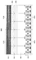
도 12는, 세로 4유닛, 가로 5유닛의 합계 20유닛의 필터 뱅크로 구성되는 분광 디바이스에서 얻어지는 2차원 분광 맵의 개략도이다.Fig. 12 is a schematic view of a two-dimensional spectral map obtained in a spectral device composed of filter banks of 20 units in total, that is, 4 units in length and 5 units in width.
도 12에서, 601이 유닛을, 602가 필터 뱅크 어레이를, 603은 촬상 이미지를, 각각 나타내고 있다.In Fig. 12,
각 유닛(601)은, K*L종류(여기서 K, L은 1 이상의 정수)의 필터로 이루어지는 필터 뱅크로 구성되어 있고, 도 11에서 도시한 바와 같이, 각각은 공간 해상도를 갖지 않는 분광 스펙트럼의 재현 기능을 갖는다.Each
또한, 그 필터 뱅크가 어레이형상으로 배치되어 필터 뱅크 어레이가 형성되어 있다. 즉, 도 12에서는, 4x5=20화소 상당의 2차원 분광 촬상 이미지(603)가 생기게 된다.In addition, the filter banks are arranged in an array, and a filter bank array is formed. That is, in Fig. 12, a 2-dimensional
다음에, 고체 촬상 소자를 필터 뱅크의 1유닛의 반분의 간격으로 시프트시키면서 각각의 장소에서 색 스펙트럼을 촬영함으로써 공간 해상도를 올리는 수법에 관해 개략 설명한다.Next, a method of increasing the spatial resolution by taking a picture of the color spectrum at each place while shifting the solid-state image pickup devices at half intervals of one unit of the filter bank will be described.
도 13은, 본 실시 형태에 관한 고체 촬상 소자를 필터 뱅크의 1유닛의 반분의 간격으로 시프트시키면서 각각의 장소에서 색 스펙트럼을 촬영함으로써 공간 해상도를 올리는 수법에 관해 개략 설명하기 위한 도면이다.13 is a view for schematically explaining a method of increasing the spatial resolution by taking a picture of a color spectrum at each place while shifting the solid-state image pickup device according to the present embodiment at half intervals of one unit of the filter bank.
우선, 최초의 스텝 ST1에서는, 센서는 위치(A)에 있다(1.A). 위치(A)에서의 촬영을 마치면 다음의 스텝에서는 위치(B)로 시프트한다(2. B).First, in the first step ST1, the sensor is at position A (1.A). When shooting at position (A) is finished, shift to position (B) in the next step (2.B).
그 다음의 스텝 ST2에서는, 위치(C)로 시프트(3. C)한다.In the next step ST2, the shift to the position C is performed (3. C).
그 다음의 스텝 ST3에서는, 위치(D)로 시프트한다(4. D).In the next step ST3, the position is shifted to the position D (4.D).
그리고, 스텝 ST4에서 위치(D)로부터 위치(A)로 시프트함으로써, 최초의 위치로 돌아온다(5. A). 이들 각각의 위치(A, B, C, D)에서 촬영을 행하고, 각각의 파장 데이터를 합성함으로써, 보다 해상도가 높은 2차원 분광 이미징이 가능해진다.Then, by shifting from position D to position A in step ST4, it returns to the initial position (5.A). By taking images at the respective positions A, B, C, and D and synthesizing the respective wavelength data, two-dimensional spectral imaging with higher resolution becomes possible.
이와 같이, 본 실시 형태의 고체 촬상 소자는, 촬상 소자를 2차원 화소가 전개되는 평면과 수평한 면 내에 미소 거리만큼 시프트하는 기능을 갖는다. 그 촬상 소자를 시프트시키는 타이밍은 화소 출력의 판독 프레임 시간 등의 센서의 판독 타이밍에 동기하는 기준 시간에 대응한다.As described above, the solid-state image pickup device of the present embodiment has a function of shifting the image pickup element by a small distance in a plane parallel to the plane on which the two-dimensional pixel is developed. The timing of shifting the image pickup element corresponds to a reference time synchronizing with the read timing of the sensor such as the readout frame time of the pixel output.
또한, 상술한 바와 같이, 고체 촬상 소자는, 촬상 소자를 2차원 화소 평면에 수평한 면 내로 미소 거리만큼 시프트하는 기능을 가지며, 그 시프트량은 필터 뱅크 1유닛의 X축Y축방향의 사이즈의 반분, 또는 그 정수분의 1에 상당하는 시프트량이다.As described above, the solid-state image pickup device has a function of shifting the image pickup element into a plane horizontal to the two-dimensional pixel plane by a small distance, and the shift amount is set to a value corresponding to the size of the
2차원 촬상 소자는 미소 거리만큼 센서를 시프트시킬 때마다, 각 화소로부터의 분광 데이터를 취득할 수 있다. 또한, 시프트량의 조합 패턴의 종류분만큼 취득한 거친 공간 분해능으로의 분광 데이터 세트를 합성함으로써, 보다 세밀한 공간 분해능을 갖는 2차원 맵을 합성할 수 있다.The two-dimensional image pickup element can acquire the spectral data from each pixel every time the sensor is shifted by a small distance. Further, by combining spectral data sets with coarse spatial resolution obtained by the kind of the combination pattern of the shift amount, a two-dimensional map having finer spatial resolution can be synthesized.
다음에, 본 실시 형태의 분광 촬상 시스템이 유지하는 필터 투과율의 데이터베이스의 구성 방법에 관해 설명한다.Next, a method of configuring a database of the filter transmittance held by the spectral imaging system of the present embodiment will be described.
도 14는, 본 실시 형태의 분광 촬상 시스템이 유지하는 필터 투과율의 데이터베이스의 교정 방법에 관해 도시하는 플로 차트이다.Fig. 14 is a flowchart showing a calibration method of the database of the filter transmittance held by the spectral imaging system of the present embodiment.
이 방법에서는, 교정 모드가 되면(ST11), 데이터베이스의 교정을 행하는지의 여부의 판별을 행한다(ST12).In this method, when the calibration mode is entered (ST11), it is determined whether or not the database is to be calibrated (ST12).
교정을 행하는 경우에는, 데이터베이스는 표준 광원을 촬영함으로써 (ST13), 새롭게 재기록 갱신할 수 있다(ST14). 이에 의해, 필터 특성이나 센서 특성, 시스템의 장년(長年)의 경시 열화가 있는 경우에도, 높은 재현성을 유지할 수 있다.In the case of performing the calibration, the database can newly renew the image by shooting a standard light source (ST13) (ST14). As a result, high reproducibility can be maintained even in the case of filter characteristics, sensor characteristics, and aged deterioration of the system over a long period of time.
또한, 데이터베이스의 교정을 행하지 않는 경우에는, 데이터베이스의 갱신은 행하여지지 않는다(ST15).When the database is not calibrated, the database is not updated (ST15).
<6. 분광 촬상 시스템의 구성례><6. Configuration Example of Spectral Imaging System>
도 15는, 본 실시 형태의 분광 촬상 시스템의 구성례를 도시하는 블록도이다.15 is a block diagram showing a configuration example of the spectral imaging system of the present embodiment.
도 15의 분광 촬상 시스템(700)은, 센서 모듈(701), 광학계(702), 모듈 제어부(703), 광학계 제어부(704), 광원 제어부(705), DSP(신호 처리부)(706), 및 촬상 소자 제어부(707)를 갖는다.15 includes a
또한 분광 촬상 시스템(700)은, 화상·스펙트럼 신호 처리부(708), 데이터베이스(709), 기록부(710), 마이크로 프로세서(711), 및 유저 인터페이스(712)를 갖는다.The
분광 촬상 시스템(700)에서, 모듈 제어부(703), 광학계 제어부(704), 광원 제어부(705), 촬상 소자 제어부(707), 화상·스펙트럼 신호 처리부(708), 데이터베이스(709), 기록부(710), 마이크로 프로세서(711)는 버스(BS)에 의해 접속되어 있다.In the
유저 인터페이스(712)를 통하여 입력된 유저에 의한 촬상 처리 등을 받아 마이크로 프로세서(711)가 전체적인 제어를 행한다.The
센서 모듈(701)은, 상술한 본 실시 형태에 관한 고체 촬상 소자(7011)(도 1의 고체 촬상 소자(100) 등), 및 액추에이터(7012)가 실장되어 있다.The
고체 촬상 소자(7011)를 시프트시키는 기구인 액추에이터(7012)는, 정전 액추에이터, 폴리머 액추에이터, 형상 기억 합금 등으로 형성된다.The
모듈 제어부(703)는, 센서 모듈(701)의 모듈 광학계를 제어하는 제어부(7031), 액추에이터(7012)를 제어하는 제어부(7032)를 포함하고, 센서 모듈(701)의 구동계의 제어를 행한다.The
광학계(702)는, 대물 렌즈(7021)나 고체 촬상 소자(7011)의 수광면의 피사체상을 결상하는 결상 렌즈(7022) 등을 포함하여 구성되고, 광학계 제어부(704)에 의해 제어된다.The
광원 제어부(705)는, LED 광원(7051)이나 레이저 광원(7052)의 제어를 행한다.The light
이와 같이, 책 시스템은 레이저나 LED 광원 등 가시 파장 및 근적외선의 특정 파장으로 고휘도의 광원 출력을 구비하고 있다.As described above, the book system is provided with a high-luminance light source output at a specific wavelength of a visible wavelength and near infrared rays such as a laser or an LED light source.
센서 모듈(701)에서 얻어지는 촬상 데이터는, DSP(706), 촬상 소자 제어부(707)를 통하여 소정의 처리를 받았던 후, 화상·스펙트럼 신호 처리부(708) 등에 전송된다.The image pickup data obtained by the
화상·스펙트럼 신호 처리부(708)에서, 상술하는 것 같았던 스펙트럼 파도의 유추 등의 신호 처리가 행하여진다. 이때, 데이터베이스(709)가 상술한 바와 같이 적절히 액세스되고, 필요에 응하여 갱신 처리 등이 행하여진다.In the image / spectral
화상·스펙트럼 신호 처리부(708)는, 예를 들면 기억부가 유지하는 데이터베이스(709)의 각 필터의 투과율 정보와 각 화소 출력과의 곱합 연산에 의해 입력 스펙트럼을 추정하는 신호 복원 기능을 갖는다.The image / spectral
<7. 금속 박막 필터의 제조 방법><7. Manufacturing Method of Metal Thin Film Filter>
이하에서는, 본 분광 촬상 디바이스에서의 금속 박막 필터의 제조 방법에 관해 개략을 기술한다.Hereinafter, a method of manufacturing a metal thin film filter in the present spectral imaging device will be schematically described.
단, 본 금속 박막 필터의 구조를 고정밀도로 실현할 수 있는 것이면, 하기에 기술하는 제조 방법으로 한정하지 않는다. 또한, 여기서는 일반적인 CMOS형 고체 촬상 소자의 제조 프로세스에서 널리 사용되고 있는 알루미늄을 통하여, 본 구조체를 실장하는 수법에 관해 설명하고 있지만, 당연히, 그 이외의 도체, 예를 들면 Ag, Au 등이라도 상관없다.However, the manufacturing method described below is not limited as long as the structure of the metal thin film filter can be realized with high accuracy. Although the method of mounting the present structure by means of aluminum widely used in the manufacturing process of a general CMOS type solid-state image pickup device is explained here, it is of course possible to use other conductors, for example, Ag, Au or the like.
본 구조는 고체 촬상 소자의 광검출 소자 윗면에 실리콘 산화막 등의 평활화층을 형성하고, 그 상층에 도체 박막을 배치한 구조를 기본으로 한다.This structure is based on a structure in which a smoothing layer such as a silicon oxide film is formed on the upper surface of a photodetector of a solid-state image sensor, and a conductor thin film is arranged on the smoothing layer.
당연하지만, 본 구조 이하의 광검출부는 일반적인 CMOS형 고체 촬상 소자면 좋고, 나아가서는 CMOS형 고체 촬상 소자로 한하지 않고 CCD형 고체 촬상 소자라도 상관없다. 따라서 광전 변환 소자의 구조 및 제조 방법에 관해서는 주지의 방법을 적용 가능하고, 여기서는 그 설명은 생략한다.Naturally, the photodetecting portion of the present structure or less may be a general CMOS type solid-state image pickup device, and furthermore, it is not limited to a CMOS type solid-state image pickup device and may be a CCD type solid-state image pickup device. Therefore, a well-known method is applicable to the structure and the manufacturing method of the photoelectric conversion element, and a description thereof will be omitted here.
우선, 금속 박막 필터를 실장하는 베이스가 되는 평활화층을 플라즈마 CVD법 등에 의해 실리콘 산화막을 적층시킴에 의해 실현한다.First, a smoothing layer serving as a base for mounting a metal thin film filter is formed by stacking a silicon oxide film by a plasma CVD method or the like.
그 위에, 금속 박막 필터의 베이스가 되는 금속 박막을 스퍼터링 등으로 적층한다. 금속 박막에 필터 기능을 만들어넣는 미세 구조는, 전자 빔 리소그래피, 포토 리소그래피, 간섭 노광법, 에칭 등의 기술에 의해 제작한다.A metal thin film serving as a base of the metal thin film filter is stacked thereon by sputtering or the like. The microstructure for forming a filter function in a metal thin film is produced by techniques such as electron beam lithography, photolithography, interference exposure, and etching.
에칭은 이방성 드라이 에칭이 바람직하고, 에칭에 이용한 가스는 4불화메탄(CF4)계의 에칭 가스가 알맞다.Anisotropic etching is dry etching is preferable, using the etching gas is suitable that the etching gas of tetrafluoromethane (CF 4) system.
그 밖에, 6불화유황, 트리플루오로메탄, 2불화크세논 등도 알맞다. 그 밖에, 전자 빔 리소그래피에 의해 기본 구조의 나노 스탬퍼를 제작하고, 나노 임프린트 기술에 의해 구조를 전사하여도 상관없다.In addition, sulfur hexafluoride, trifluoromethane, xenon hexafluoride and the like are also suitable. In addition, the nano stamper of the basic structure may be manufactured by electron beam lithography, and the structure may be transferred by the nanoimprint technique.
다음에, 금속 박막 필터의 공극부를 충전하는 층간 절연막을 플라즈마 CVD법 등에 의해 적층한다. 여기서 플라즈마 CVD법을 이용하는 것은, 감압 CVD법에 비하여 상대적으로 낮은 온도(250℃ 내지 400℃)에서의 성막이 가능하기 때문에, Al 등의 금속으로 만들어진 금속 박막 필터를 실장한 후에 보호막을 형성하는데 유리하기 때문이다.Next, an interlayer insulating film for filling the gap portion of the metal thin film filter is laminated by plasma CVD or the like. The use of the plasma CVD method is advantageous in that a film can be formed at a relatively low temperature (250 DEG C to 400 DEG C) as compared with the low pressure CVD method, and therefore, a glass thin film filter made of a metal such as Al .
당연하지만, 그 밖의 수법에 의해서도 금속 박막 성막 후에 이용하는 것이 가능한 수법이라면, 상기 수법으로 한정되지는 않는다.Naturally, however, the present invention is not limited to the technique described above, as long as it can be used after the metal thin film formation by any other technique.
또한, 가시 파장대역에서 이용한 절연층의 매질로서는, 산화실리콘(SiO2) 및 SiO2를 주성분으로 하는 복합 소재가 알맞다. 그 밖에 불화마그네슘(MgF2) 등을 이용할 수 있다.Further, as a medium of the insulating layer used in the visible wavelength band, a composite material containing silicon oxide (SiO 2 ) and SiO 2 as a main component is suitable. Magnesium fluoride (MgF 2 ) or the like may be used.
그 밖에, 굴절률이 커지지만, 질화실리콘(Si3N4), 산화티탄(TiO2), 산화탄탈륨(Ta2O5), 산화지르코늄(ZrO2), 산화니오브(Nb2O5), 산화하프늄(HfO2) 등의 산화물, 질화물을 사용할 수도 있In addition, only the refractive index is large, the silicon nitride (Si3N4), titanium (TiO 2), tantalum oxide (Ta 2 O 5), zirconium oxide (ZrO 2), niobium oxide (Nb 2 O5), hafnium oxide (HfO 2 ), And the like may be used.
도 16은, 금속 박막 필터의 제조 장치의 개략 구성을 도시하는 도면이다.16 is a diagram showing a schematic configuration of an apparatus for manufacturing a metal thin film filter.
도 16의 제조 장치(800)는, 고주파 전원(801, 803), 임피던스 정합기(802, 804), 기판(805), 타겟(806), 진공 듀어(807) 등을 포함하여 구성되어 있다.16 includes high
기판(805)은, 임피던스 정합기(802)를 통하여 고주파 전원(801)에 접속된다.The
또한, 타겟(806)도 마찬가지로 임피던스 정합기(804)를 통하여 고주파 전원(803)에 접속된다.The
여기서 고주파 전원은, 일반적으로 주파수가 13.56MHz인 것이 많다.The high frequency power source generally has a frequency of 13.56 MHz in many cases.
진공 듀어(807) 중에는, 불활성 가스(예를 들면 Ar 가스)를 주성분으로 하는 혼합 가스를 충전하고, 전형적으로는 0.1 내지 10mTorr 정도의 가스 압력이 알맞다.The
타겟(806) 및 기판(805)에 고주파 전원(803, 801)에 의한 전력을 공급함으로써 플라즈마를 생성시킨다. 타겟(806)에 교류 전압을 인가함으로써, 탐침(探針) 특성의 비선형성에 의한 직류 바이어스(자기(自己) 바이어스 효과)가 걸려서 타겟(806)은 시간 평균으로 부전위가 된다.The plasma is generated by supplying power to the
따라서 정전하를 갖는 기체 이온은 전위차에 의한 운동 에너지를 획득하여 타겟(806)에 충돌한다. 이 반응에 의해 타겟 물질의 표면의 원자·분자가 비산하고, 그 물질 입자가 기판(805)에 부착하여 기판(805)상에 박막이 적층된다.Accordingly, the gas ions having the electrostatic charge acquire the kinetic energy due to the potential difference, and collide with the
한편으로, 기판(805)에도 고주파 전원(801)과 임피던스 정합기(802)가 접속되어 있다. 그 때문에, 기판(805)에 공급하는 전력, 가스의 종류, 압력을 조정함으로써, 충돌한 이온의 종류, 운동 에너지의 대소, 스퍼터링의 효과를 제어할 수 있다.On the other hand, a high
스퍼터링에 의한 성막 효과를 수반하지 않는, 단독의 스퍼터 에칭을 행한 경우에는, 기판(805)에만 고주파 전원을 공급하면 좋다.In the case where a single sputter etching is performed without accompanying a deposition effect by sputtering, a high frequency power supply may be supplied only to the
또한 성막할 때에, CF4 등의 가스류량을 조정하면서 성막을 행함으로써, SiO2의 굴절률은 좁은 범위로 컨트롤할 수 있다.In addition, when film formation is performed while adjusting the amount of gas such as CF 4 , the refractive index of SiO 2 can be controlled within a narrow range.
그 때문에, 화소 영역을 복수로 분할하여, 영역마다 다른 굴절률을 갖는 유전체막을 실장하는 것이 가능해진다. 그에 의해, 금속 박막 필터의 가공 패턴이 공통이라도, 플라즈몬 공명 파장이 미묘하게 변화하고, 그 결과, 보다 다수 종류의 필터의 실장이 가능해지고, 보다 높은 파장 분해능(고분산)에서의 분광 데이터의 취득이 가능해진다.Therefore, the pixel region can be divided into a plurality of regions, and a dielectric film having a refractive index different from region to region can be mounted. Thereby, even if the processing pattern of the metal thin film filter is common, the plasmon resonance wavelength slightly changes, and as a result, mounting of more kinds of filters becomes possible, and acquisition of spectroscopic data at a higher wavelength resolution Lt; / RTI >
이상 설명한 바와 같이, 본 실시 형태에 의하면, 이하의 효과를 얻을 수 있다.As described above, according to the present embodiment, the following effects can be obtained.
단일의 칩으로 고감도의 분광 스펙트럼이 가능해진다. 금속 박막 필터의 단독 필터 사이즈와 고체 촬상 소자의 단 화소의 사이즈가 달라도, 촬상 화소의 인접 화소 사이에서 필터를 공유함으로써 다음의 이점을 제공한다.A single chip enables a highly sensitive spectral spectrum. Sharing the filter between adjacent pixels of a picked-up pixel provides the following advantages, although the single filter size of the metal thin film filter and the size of the single pixel of the solid-state image pickup device are different.
즉, 전용의 고체 촬상 소자가 아니라도, 필터를 실장하는 것만으로 분광·촬상 기능이 실현될 수 있고, 보다 염가로 고성능의 분광·촬상 디바이스를 실현할 수 있다.That is, even if the solid-state imaging device is not a dedicated solid-state imaging device, the spectroscopic and imaging function can be realized by simply mounting a filter, and a spectroscopic / imaging device with higher performance can be realized more inexpensively.
동일 패턴의 금속 박막 필터라도 굴절률을 X종류로 늘리는 것으로, 실효적으로 필터의 종류를 X배가 되는 것이 가능해지고, 그 결과, 보다 높은 파장 분해능으로 분광·촬상하는 것이 가능해진다.It is possible to effectively increase the type of the filter by X times by increasing the refractive index to X types even with the metal thin film filter of the same pattern. As a result, it becomes possible to perform spectroscopic imaging with higher wavelength resolution.
공간 해상도가 높은 2차원 분광 매핑이 가능해진다. 8x8화소나 16x16화소라는 비교적 규모가 큰 범위에서의 인접 화소 사이에서 금속 박막 필터를 공유하기 때문에, 기존의 수법에서는 2차원 분광 매핑을 행할 때에, 공간 해상도가 크게 저하되는 문제가 있다. 본 기술에 의한 화소 시프트법을 조합시킴으로써, 보다 높은 2차원 분광 촬상이 염가의 실현이 가능해진다.Dimensional spectral mapping with high spatial resolution becomes possible. Since the metal thin film filter is shared between adjacent pixels in a relatively large scale range of 8x8 pixels or 16x16 pixels, there is a problem that the spatial resolution is largely lowered when the two-dimensional spectral mapping is performed in the conventional technique. By combining the pixel shift method according to the present technology, it is possible to realize a lower cost at higher two-dimensional spectral imaging.
N종류의 필터의 투과 특성 데이터베이스를 유지, 더욱 그 갱신이 가능하는 기능을 갖음으로써, 그 데이터와 출력 화소치와의 곱합 연산에 의해 입력 스펙트럼을 고정밀도로 복원하는 것이 가능해진다.It is possible to restore the input spectrum with high accuracy by performing a multiplication operation of the data and the output pixel value by having the function of maintaining and updating the transmission characteristic database of the N kinds of filters.
회절 격자 등의 협대역 필터와 달리, 각각의 필터는 협대역이 아니기 때문에, 광을 효율적으로 사용하고, 계산에 의해 입력 스펙트럼을 추정하는 수법이기 때문에, 고파장 분해능과 고감도의 양립이 가능해진다.Unlike narrow-band filters such as diffraction gratings, since each filter is not narrow-band, it is a technique of efficiently using light and estimating an input spectrum by calculation, and therefore, high wavelength resolution and high sensitivity can be compatible.
또한, 본 기술은 이하와 같은 구성도 취할 수 있다.The present technology can also take the following configuration.
(1) 광전 변환 소자를 포함하는 화소가 어레이형상으로 배열된 2차원 화소 어레이와,(1) a two-dimensional pixel array in which pixels including photoelectric conversion elements are arranged in an array;
상기 2차원 화소 어레이의 화소 영역에 대향하도록 배치되고, 검출하여야 할 파장보다도 짧은 주기적인 미세 패턴을 갖는 분광 기능을 구비한 복수종류의 필터를 가지며,And a plurality of kinds of filters arranged to face the pixel region of the two-dimensional pixel array and having a spectroscopic function having a periodic fine pattern that is shorter than a wavelength to be detected,
상기 각 필터는,Each of the above-
상기 2차원 화소 어레이의 각 화소의 광전 변환 소자보다도 크고, 인접하는 복수의 광전 변환 소자군에 대해 1종류의 필터가 배치된 하나의 유닛을 형성하고,One unit in which one kind of filter is arranged for a plurality of adjacent photoelectric conversion element groups is formed larger than the photoelectric conversion element of each pixel of the two-dimensional pixel array,
상기 복수종류의 필터는,Wherein the plurality of kinds of filters
인접하는 유닛군에 대해 배치되어 필터 뱅크를 형성하고,A filter bank is formed for the adjacent unit groups,
상기 필터 뱅크가 상기 2차원 화소 어레이의 화소 영역에 대향하도록, NxM유닛(단, N, M은 1 이상의 정수) 배치되어 있는 고체 촬상 소자.And NxM units (where N and M are integers equal to or larger than 1) are arranged such that the filter banks face the pixel regions of the two-dimensional pixel array.
(2) 상기 필터는,(2)
검출하여야 할 파장보다도 짧은 주기적인 미세 가공 패턴을 갖는 금속 박막 필터를 포함하고,A metal thin film filter having a periodic fine processing pattern shorter than a wavelength to be detected,
상기 금속 박막 필터는,The metal thin-
플라즈마 주파수가 자외선역·가시 파장역에 있는 금속에 의해 형성되고,The plasma frequency is formed by the metal in the ultraviolet ray / visible wavelength region,
서브미크론 스케일의 간격으로 요철부, 또는 구멍 구조가 주기적으로 배치된 1차원 격자 또는 2차원 격자인 상기 (1) 기재의 고체 촬상 소자.A solid-state image pickup element according to the above (1), wherein the solid-state image pickup element is a one-dimensional lattice or a two-dimensional lattice in which recesses and protrusions are arranged at intervals of a submicron scale, or hole structures are periodically arranged.
(3) 상기 금속 박막 필터는,(3) The metal thin-
검출하여야 할 소망하는 전자파 파장대역 내의 특정한 전자파를 선택적으로 흡수·투과시키는 필터링 기능을 가지며, 당해 필터가 갖는 요철부 또는 구멍 구조의 주기 패턴 사이의 공극은, 중공 구조 또는 유전체로 충전되어 있는 상기 (2) 기재의 고체 촬상 소자.And the filter has a filtering function for selectively absorbing and transmitting a specific electromagnetic wave within a desired electromagnetic wave wavelength band to be detected, and the gap between the periodic patterns of the concavo-convex portion or the hole structure of the filter has a function of ( 2) based solid-state imaging element.
(4) 상기 금속 박막 필터는,(4) The metal thin-
검출하여야 할 소망하는 전자파 파장대역 내의 특정한 전자파를 선택적으로 흡수·투과시키는 필터링 기능을 가지며, 당해 필터가 갖는 요철부 또는 구멍 구조의 주기 패턴 사이의 공극은 유전체로 충전되어 있고, 또한 복수 있는 필터 뱅크중 적어도 하나의 필터 뱅크는 다른 필터 뱅크와는 다른 굴절률을 갖는 유전체로 그 공극부가 충전되어 있는 상기 (2) 기재의 고체 촬상 소자The filter has a function of selectively absorbing and transmitting a specific electromagnetic wave within a desired electromagnetic wave wavelength band to be detected. The air gap between the periodic patterns of the concavo-convex portion or the hole structure of the filter is filled with a dielectric, Wherein at least one filter bank of the solid-state imaging element (2) has a refractive index different from that of the other filter banks,
(5) 상기 금속 박막 필터는,(5) The metal thin-
유전체로 이루어지는 평활화층의 상층에 배치되어 있는 상기 (2)부터 (4)의 어느 하나에 기재된 고체 촬상 소자.The solid-state imaging element according to any one of (2) to (4), wherein the solid-state imaging element is disposed on an upper layer of a smoothing layer made of a dielectric.
(6) 상기 금속 박막 필터는,(6) The metal thin-
유전체에 의해 형성되는 평활화층의 상층에 배치되고, 당해 유전체의 평활화층의 굴절률은 상기 화소 영역의 복수 영역에서 각각이 다른 굴절률을 갖는 상기 (2)부터 (4)의 어느 하나에 기재된 고체 촬상 소자.The solid-state imaging device according to any one of (2) to (4), wherein the refractive index of the smoothing layer of the dielectric is different from that of each of the plurality of regions in the pixel region, .
(7) 상기 화소 영역에 대향하여 배치된 상기 금속 박막 필터의 각 필터는,(7) Each filter of the metal thin film filter disposed opposite to the pixel region,
2차원 화소 어레이를 형성하는 각 화소와 동등 또는 그보다도 넓은 면적을 가지며, 인접하는 가로(X축방향) U화소, 세로(Y축방향) V화소로 형성되는 화소군에 대해 1종류의 필터가 배치되는 상기 (2)부터 (6)의 어느 하나에 기재된 고체 촬상 소자. One type of filter is used for a pixel group having an area equal to or wider than that of each pixel forming the two-dimensional pixel array and formed of adjacent horizontal (X axis direction) U pixels and vertical (Y axis direction) V pixels The solid-state imaging device according to any one of (2) to (6) above, wherein the solid-state imaging element is arranged.
여기서, U, V는 1 이상의 정수이다.Here, U and V are integers of 1 or more.
(8) 상기 필터는,(8)
X축방향으로 K종류, Y축방향으로 L종류 있고,There are K types in the X axis direction and L types in the Y axis direction,
각각의 필터군은 K*L종류의 필터로 1개의 필터 뱅크 유닛을 형성하고, 당해 필터 뱅크를 1유닛 이상 갖는 상기 (1)부터 (7)의 어느 하나에 기재된 고체 촬상 소자.The solid-state image pickup element according to any one of (1) to (7), wherein each filter group forms one filter bank unit with a K * L type filter and has one or more filter banks.
여기서, K, L은 각각 1 이상의 정수이다.Here, K and L are integers of 1 or more, respectively.
(9) 배치된 상기 필터 뱅크는,(9) The filter bank arranged,
X축방향으로 N종류, Y축방향으로 M종류 있는 상기 (8) 기재의 고체 촬상 소자.The solid-state imaging device according to (8), wherein N types are arranged in the X-axis direction and M types are arranged in the Y-axis direction.
여기서, N, M은 각각 1 이상의 정수이다.Here, N and M are integers of 1 or more, respectively.
(10) 상기 필터 뱅크의 각 필터의 전자파 파장마다의 투과율 정보를 데이터베이스로서 유지하는 기억부를 갖는 상기 (1)부터 (9)의 어느 하나에 기재된 고체 촬상 소자.(10) The solid-state image pickup device according to any one of (1) to (9), wherein the solid-state image pickup element has a storage section for holding transmittance information for each wavelength of electromagnetic waves of each filter of the filter bank as a database.
(11) 상기 필터 뱅크의 각 필터의 파장마다의 투과율 정보를 데이터베이스로서 유지하는 기억부를 가지며,(11) The liquid crystal display device according to any one of (11) to (11), further comprising a storage unit for holding transmittance information for each wavelength of each filter of the filter bank as a database,
상기 데이터베이스는,The database includes:
기준 광원을 촬영함으로써 재교정정 및 갱신이 가능한 상기 (1)부터 (9)의 어느 하나에 기재된 고체 촬상 소자.The solid-state image pickup device according to any one of (1) to (9), wherein the reference light source can be re-corrected and updated by photographing.
(12) 상기 기억부가 유지하는 데이터베이스의 각 필터의 투과율 정보와 각 화소 출력과의 곱합 연산에 의해 입력 스펙트럼을 추정하는 신호 처리부를 갖는 상기 (10) 또는 (11) 기재의 고체 촬상 소자.(12) The solid-state imaging device according to (10) or (11), wherein the solid-state image pickup element has a signal processing section for estimating an input spectrum by a multiplication operation of transmittance information of each filter of the database held by the storage section and each pixel output.
(13) 상기 2차원 화소 어레이에 의해 형성되는 촬상 소자는, 화소가 2차원으로 전개되는 평면과 수평한 면 내에 미소 거리만큼 시프트하는 기구를 가지며,(13) The imaging device formed by the two-dimensional pixel array has a mechanism for shifting a pixel by a minute distance in a plane parallel to the two-dimensional development plane,
상기 촬상 소자를 시프트시키는 타이밍은 화소 출력의 판독 프레임 시간 등의 센서의 판독 타이밍에 동기하는 기준 시간에 대응하는 상기 (1)부터 (12)의 어느 하나에 기재된 고체 촬상 소자.The solid-state imaging device according to any one of (1) to (12) above, wherein the timing for shifting the imaging element corresponds to a reference time synchronized with a read timing of the sensor such as a reading frame time of the pixel output.
(14) 상기 2차원 화소 어레이에 의해 형성되는 촬상 소자는, 화소가 2차원으로 전개되는 평면과 수평한 면 내에 미소 거리만큼 시프트하는 기구를 가지며,(14) The imaging device formed by the two-dimensional pixel array has a mechanism for shifting a pixel by a minute distance in a plane parallel to the two-dimensional development plane,
그 시프트량은 필터 뱅크 1유닛의 X축Y축방향의 사이즈의 반분, 또는 그 정수분의 1에 상당하는 시프트량이고,The shift amount is a shift amount corresponding to one half of the size of the
상기 촬상 소자를 미소 거리만큼 센서를 시프트시킬 때마다, 각 화소로부터의 분광 데이터를 취득하고, 또한 시프트량의 조합 패턴의 종류분만큼 취득한 거칠은 공간 분해능으로의 분광 데이터 세트를 합성함으로써, 보다 세밀한 공간 분해능을 갖는 2차원 맵을 합성하는 처리부를 갖는 상기 (1)부터 (13)의 어느 하나에 기재된 고체 촬상 소자.By acquiring the spectroscopic data from each pixel each time the sensor is shifted by a minute distance of the image pickup device and synthesizing the spectroscopic data set with the coarse spatial resolution acquired by the amount of the combination pattern of the shift amount, A solid-state imaging device according to any one of (1) to (13), wherein the solid-state imaging device has a processing section for synthesizing a two-dimensional map having spatial resolution.
(15) CMOS형 고체 촬상 소자이고,(15) A CMOS solid-state image pickup device,
상기 각 화소는 화소마다 온 칩 집광소자를 구비하고, 상기 집광소자보다도 굴절률이 작은 소재를 온 칩 집광소자의 상층에 적층함으로써, 집광 기능을 유지한 채로 평활화층이 배치되고, 당해 평활화층상에 상기 필터가 배치되어 있는 상기 (1)부터 (14)의 어느 하나에 기재된 고체 촬상 소자.Wherein each pixel has an on-chip light-converging element for each pixel, and a material having a refractive index lower than that of the light-converging element is stacked on an upper layer of the on-chip light-converging element so that the smoothing layer is disposed while maintaining the light- A solid-state imaging device according to any one of (1) to (14), wherein a filter is disposed.
(16)(16)
상기 필터는,The filter includes:
고굴절률의 매질과 저굴절률의 매질을 적층한 전자파 파장을 투과시키는 광학 필터를 포함하는 상기 (1), (8)부터 (15)의 어느 하나에 기재된 고체 촬상 소자.The solid-state image pickup device according to any one of (1), (8) to (15), wherein the solid-state image pickup element comprises an optical filter that transmits electromagnetic waves having a medium of a high refractive index and a medium of a low refractive index.
(17) 고체 촬상 소자와,(17) A solid-
상기 고체 촬상 소자의 2차원 화소 어레이부에 피사체상을 결상하는 광학계를 가지며,Wherein the solid-state image sensor has an optical system for imaging a subject image on a two-dimensional pixel array portion of the solid-
상기 고체 촬상 소자는,The solid-
광전 변환 소자를 포함하는 화소가 어레이형상으로 배열된 2차원 화소 어레이와,A two-dimensional pixel array in which pixels including photoelectric conversion elements are arranged in an array;
상기 2차원 화소 어레이의 화소 영역에 대향하도록 배치되고, 검출하여야 할 파장보다도 짧은 주기적인 미세 패턴을 갖는 분광 기능을 구비한 복수종류의 필터를 가지며,And a plurality of kinds of filters arranged to face the pixel region of the two-dimensional pixel array and having a spectroscopic function having a periodic fine pattern that is shorter than a wavelength to be detected,
상기 각 필터는,Each of the above-
상기 2차원 화소 어레이의 각 화소의 광전 변환 소자보다도 크고, 인접하는 복수의 광전 변환 소자군에 대해 1종류의 필터가 배치된 하나의 유닛을 형성하고,One unit in which one kind of filter is arranged for a plurality of adjacent photoelectric conversion element groups is formed larger than the photoelectric conversion element of each pixel of the two-dimensional pixel array,
상기 복수종류의 필터는,Wherein the plurality of kinds of filters
인접하는 유닛군에 대해 배치되어 필터 뱅크를 형성하고,A filter bank is formed for the adjacent unit groups,
상기 필터 뱅크가 상기 2차원 화소 어레이의 화소 영역에 대향하도록, NxM유닛(단, N, M은 1 이상의 정수) 배치되어 있는 촬상 시스템.And NxM units (where N and M are integers equal to or larger than 1) are arranged so that the filter banks face the pixel regions of the two-dimensional pixel array.
100 : 촬상 소자
110 : 화소 어레이부
110A : 화소
111 : 포토 다이오드(광전 변환 소자)
112 : 전송 트랜지스터
113 : FD
114 : 증폭 트랜지스터
115 : 선택 트랜지스터
116 : 리셋 트랜지스터
120 : 수직 주사 회로
130 : 수평 전송 주사 회로
140 : 칼럼 ADC 회로
150 : PLL 회로
160 : DAC(디지털-아날로그 컨버터)
170 : 센스 앰프 회로(S/A)
201 : 2차원 화소군(화소 어레이부)
202 : 금속 박막 필터군(필터 뱅크, 유닛)
203 : 필터 뱅크 어레이
300 : 금속 박막 필터
500, 500A 내지 500E : 고체 촬상 소자
501 : 온 칩 마이크로 렌즈
502A, 502B, 502C : 금속 박막 필터
503 : 평활화층
504 : 포토 다이오드
505 : 신호 배선층
506A, 506B, 506C : 인접 화소
507, 507A : 평활화층
512A, 512B : 포토닉 필터
700 : 분광 촬상 시스템
701 : 센서 모듈
702 : 광학계
703 : 모듈 제어부
704 : 광학계 제어부
705 : 광원 제어부
706 : DSP(신호 처리부)
707 : 촬상 소자 제어부
708 : 화상·스펙트럼 신호 처리부
709 : 데이터베이스
710 : 기록부
711 : 마이크로 프로세서
712 : 유저 인터페이스100:
110: pixel array unit
110A: pixel
111: photodiode (photoelectric conversion element)
112: transfer transistor
113: FD
114: amplifying transistor
115: selection transistor
116: reset transistor
120: vertical scanning circuit
130: horizontal transfer scanning circuit
140: Column ADC circuit
150: PLL circuit
160: DAC (Digital-to-Analog Converter)
170: sense amplifier circuit (S / A)
201: two-dimensional pixel group (pixel array unit)
202: Metal thin film filter group (filter bank, unit)
203: filter bank array
300: metal thin film filter
500, 500A to 500E: solid-state image pickup device
501: On-chip micro lens
502A, 502B, 502C: metal thin film filter
503: Smoothing layer
504: Photodiode
505: signal wiring layer
506A, 506B, and 506C: adjacent pixels
507, 507A: Smoothing layer
512A, 512B: Photonic filter
700: spectroscopic imaging system
701: Sensor module
702: Optical system
703: Module control section
704: Optical system controller
705:
706: DSP (signal processor)
707:
708: Image / spectral signal processor
709: Database
710:
711: Microprocessor
712: User interface
Claims (17)
상기 2차원 화소 어레이의 화소 영역에 대향하도록 배치되고, 검출하여야 할 파장보다도 짧은 주기적인 미세 패턴을 갖는 분광 기능을 구비한 복수종류의 필터를 가지며,
상기 각 필터는,
상기 2차원 화소 어레이의 각 화소의 광전 변환 소자보다도 크고, 인접하는 복수의 광전 변환 소자군에 대해 1종류의 필터가 배치된 하나의 유닛을 형성하고,
상기 복수종류의 필터는,
인접하는 유닛군에 대해 배치되어 필터 뱅크를 형성하고,
상기 필터 뱅크가 상기 2차원 화소 어레이의 화소 영역에 대향하도록, NxM유닛(단, N, M은 1 이상의 정수) 배치되어 있는 것을 특징으로 하는 고체 촬상 소자.A two-dimensional pixel array in which pixels including photoelectric conversion elements are arranged in an array;
And a plurality of kinds of filters arranged to face the pixel region of the two-dimensional pixel array and having a spectroscopic function having a periodic fine pattern that is shorter than a wavelength to be detected,
Each of the above-
One unit in which one kind of filter is arranged for a plurality of adjacent photoelectric conversion element groups is formed larger than the photoelectric conversion element of each pixel of the two-dimensional pixel array,
Wherein the plurality of kinds of filters
A filter bank is formed for the adjacent unit groups,
Wherein NxM units (N and M are integers equal to or larger than 1) are arranged so that the filter banks face the pixel regions of the two-dimensional pixel array.
상기 필터는,
검출하여야 할 파장보다도 짧은 주기적인 미세 가공 패턴을 갖는 금속 박막 필터를 포함하고,
상기 금속 박막 필터는,
플라즈마 주파수가 자외선역·가시 파장역에 있는 금속에 의해 형성되고,
서브미크론 스케일의 간격으로 요철부, 또는 구멍 구조가 주기적으로 배치된 1차원 격자 또는 2차원 격자인 것을 특징으로 하는 고체 촬상 소자.The method according to claim 1,
The filter includes:
A metal thin film filter having a periodic fine processing pattern shorter than a wavelength to be detected,
The metal thin-
The plasma frequency is formed by the metal in the ultraviolet ray / visible wavelength region,
Dimensional lattice or two-dimensional lattice in which irregularities or hole structures are periodically arranged at intervals of submicron scale.
상기 금속 박막 필터는,
검출하여야 할 소망하는 전자파 파장대역 내의 특정한 전자파를 선택적으로 흡수·투과시키는 필터링 기능을 가지며, 당해 필터가 갖는 요철부 또는 구멍 구조의 주기 패턴 사이의 공극은, 중공 구조 또는 유전체로 충전되어 있는 것을 특징으로 하는 고체 촬상 소자.3. The method of claim 2,
The metal thin-
The filter has a filtering function for selectively absorbing and transmitting a specific electromagnetic wave within a desired electromagnetic wave wavelength band to be detected and the gap between the periodic patterns of the concavo-convex portion or the hole structure of the filter is filled with a hollow structure or a dielectric .
상기 금속 박막 필터는,
검출하여야 할 소망하는 전자파 파장대역 내의 특정한 전자파를 선택적으로 흡수·투과시키는 필터링 기능을 가지며, 당해 필터가 갖는 요철부 또는 구멍 구조의 주기 패턴 사이의 공극은 유전체로 충전되어 있고, 또한 복수 있는 필터 뱅크 중 적어도 하나의 필터 뱅크는 다른 필터 뱅크와는 다른 굴절률을 갖는 유전체로 그 공극부가 충전되어 있는 것을 특징으로 하는 고체 촬상 소자3. The method of claim 2,
The metal thin-
The filter has a function of selectively absorbing and transmitting a specific electromagnetic wave within a desired electromagnetic wave wavelength band to be detected. The air gap between the periodic patterns of the concavo-convex portion or the hole structure of the filter is filled with a dielectric, Wherein at least one of the filter banks is filled with a gap with a dielectric having a refractive index different from that of the other filter banks.
상기 금속 박막 필터는,
유전체로 이루어지는 평활화층의 상층에 배치되어 있는 것을 특징으로 하는 고체 촬상 소자.3. The method of claim 2,
The metal thin-
Wherein the solid-state imaging element is disposed on an upper layer of a smoothing layer made of a dielectric.
상기 금속 박막 필터는,
유전체에 의해 형성되는 평활화층의 상층에 배치되고, 당해 유전체의 평활화층의 굴절률은 상기 화소 영역의 복수 영역에서 각각이 다른 굴절률을 갖는 것을 특징으로 하는 고체 촬상 소자.3. The method of claim 2,
The metal thin-
Wherein the refractive index of the smoothing layer of the dielectric is different from the refractive index of the smoothing layer in a plurality of regions of the pixel region.
상기 화소 영역에 대향하여 배치된 상기 금속 박막 필터의 각 필터는,
2차원 화소 어레이를 형성하는 각 화소와 동등 또는 그것보다도 넓은 면적을 가지며, 인접하는 가로(X축방향) U화소, 세로(Y축방향) V화소로 형성되는 화소군에 대해 1종류의 필터가 배치되는 것을 특징으로 하는 고체 촬상 소자.
여기서, U, V는 1 이상의 정수이다.3. The method of claim 2,
Wherein each filter of the metal thin film filter disposed opposite to the pixel region comprises:
One type of filter is used for a pixel group which is equal to or larger than each pixel forming the two-dimensional pixel array, and which is formed of adjacent horizontal (X-axis direction) U pixels and vertical (Y axis direction) State image pickup element.
Here, U and V are integers of 1 or more.
상기 필터는,
X축방향으로 K종류, Y축방향으로 L종류 있고,
각각의 필터군은 K*L종류의 필터로 하나의 필터 뱅크 유닛을 형성하고, 당해 필터 뱅크를 1유닛 이상 갖는 것을 특징으로 하는 고체 촬상 소자.
여기서, K, L은 각각 1 이상의 정수이다.The method according to claim 1,
The filter includes:
There are K types in the X axis direction and L types in the Y axis direction,
Wherein each filter group includes one filter bank unit formed by a K * L type filter, and has one or more filter banks.
Here, K and L are integers of 1 or more, respectively.
배치되는 상기 필터 뱅크는,
X축방향으로 N종류, Y축방향으로 M종류 있는 것을 특징으로 하는 고체 촬상 소자.
여기서, N, M은 각각 1 이상의 정수이다.9. The method of claim 8,
The filter bank,
N types in the X-axis direction, and M types in the Y-axis direction.
Here, N and M are integers of 1 or more, respectively.
상기 필터 뱅크의 각 필터의 전자파 파장마다의 투과율 정보를 데이터베이스로서 유지하는 기억부를 갖는 것을 특징으로 하는 고체 촬상 소자.The method according to claim 1,
And a storage unit for storing transmittance information for each wavelength of electromagnetic waves of each filter of said filter bank as a database.
상기 필터 뱅크의 각 필터의 파장마다의 투과율 정보를 데이터베이스로서 유지하는 기억부를 가지며,
상기 데이터베이스는,
기준 광원을 촬영함으로써 재교정 및 갱신이 가능한 것을 특징으로 하는 고체 촬상 소자.The method according to claim 1,
And a storage unit for storing transmittance information for each wavelength of each filter of the filter bank as a database,
The database includes:
Wherein the reference light source is re-calibrated and updated by photographing the reference light source.
상기 기억부가 유지하는 데이터베이스의 각 필터의 투과율 정보와 각 화소 출력과의 곱합 연산에 의해 입력 스펙트럼을 추정하는 신호 처리부를 갖는 것을 특징으로 하는 고체 촬상 소자.11. The method of claim 10,
And a signal processing section for estimating an input spectrum by a multiplication operation of transmittance information of each filter of the database held by said storage section and each pixel output.
상기 2차원 화소 어레이에 의해 형성되는 촬상 소자는, 화소가 2차원으로 전개되는 평면과 수평한 면 내에 미소 거리만큼 시프트하는 기구를 가지며,
상기 촬상 소자를 시프트시키는 타이밍은 화소 출력의 판독 프레임 시간 등의 센서의 판독 타이밍에 동기하는 기준 시간에 대응하는 것을 특징으로 하는 고체 촬상 소자.The method according to claim 1,
Wherein the imaging element formed by the two-dimensional pixel array has a mechanism for shifting a pixel by a minute distance in a plane parallel to the two-
Wherein the timing for shifting the imaging element corresponds to a reference time synchronized with a reading timing of the sensor such as a reading frame time of the pixel output.
상기 2차원 화소 어레이에 의해 형성되는 촬상 소자는, 화소가 2차원으로 전개되는 평면과 수평한 면 내에 미소 거리만큼 시프트하는 기구를 가지며,
그 시프트량은 필터 뱅크 1유닛의 X축Y축방향의 사이즈의 반분, 또는 그 정수분의 1에 상당하는 시프트량이고,
상기 촬상 소자를 미소 거리만큼 센서를 시프트시킬 때마다, 각 화소로부터의 분광 데이터를 취득하고, 또한 시프트량의 조합 패턴의 종류분만큼 취득한 거칠은 공간 분해능으로의 분광 데이터 세트를 합성함으로써, 보다 세밀한 공간 분해능을 갖는 2차원 맵을 합성하는 처리부를 갖는 것을 특징으로 하는 고체 촬상 소자.The method according to claim 1,
Wherein the imaging element formed by the two-dimensional pixel array has a mechanism for shifting a pixel by a minute distance in a plane parallel to the two-
The shift amount is a shift amount corresponding to one half of the size of the filter bank 1 unit in the X-axis Y-axis direction or one of the integer numbers,
By acquiring the spectroscopic data from each pixel each time the sensor is shifted by a minute distance of the image pickup device and synthesizing the spectroscopic data set with the coarse spatial resolution acquired by the amount of the combination pattern of the shift amount, And a processing unit for synthesizing a two-dimensional map having spatial resolution.
CMOS형 고체 촬상 소자이고,
상기 각 화소는 화소마다 온 칩 집광소자를 구비하고, 상기 집광소자보다도 굴절률이 작은 소재를 온 칩 집광소자의 상층에 적층함으로써, 집광 기능을 유지한 채로 평활화층이 배치되고, 당해 평활화층상에 상기 필터가 배치되어 있는 것을 특징으로 하는 고체 촬상 소자.The method according to claim 1,
Type solid-state image pickup element,
Wherein each pixel has an on-chip light-converging element for each pixel, and a material having a refractive index lower than that of the light-converging element is stacked on an upper layer of the on-chip light-converging element so that the smoothing layer is disposed while maintaining the light- And a filter is disposed on the surface of the solid-state imaging element.
상기 필터는,
고굴절률의 매질과 저굴절률의 매질을 적층한 전자파 파장을 투과시키는 광학 필터를 포함하는 것을 특징으로 하는 고체 촬상 소자.The method according to claim 1,
The filter includes:
And an optical filter that transmits an electromagnetic wave wavelength obtained by laminating a medium having a high refractive index and a medium having a low refractive index.
상기 고체 촬상 소자의 2차원 화소 어레이부에 피사체상을 결상하는 광학계를 가지며,
상기 고체 촬상 소자는,
광전 변환 소자를 포함하는 화소가 어레이형상으로 배열된 2차원 화소 어레이와,
상기 2차원 화소 어레이의 화소 영역에 대향하도록 배치되고, 검출하여야 할 파장보다도 짧은 주기적인 미세 패턴을 갖는 분광 기능을 구비한 복수종류의 필터를 가지며,
상기 각 필터는,
상기 2차원 화소 어레이의 각 화소의 광전 변환 소자보다도 크고, 인접하는 복수의 광전 변환 소자군에 대해 1종류의 필터가 배치된 하나의 유닛을 형성하고,
상기 복수종류의 필터는,
인접하는 유닛군에 대해 배치되어 필터 뱅크를 형성하고,
상기 필터 뱅크가 상기 2차원 화소 어레이의 화소 영역에 대향하도록, NxM유닛(단, N, M은 1 이상의 정수) 배치되어 있는 것을 특징으로 하는 촬상 시스템.State image pickup device,
Wherein the solid-state image sensor has an optical system for imaging a subject image on a two-dimensional pixel array portion of the solid-
The solid-
A two-dimensional pixel array in which pixels including photoelectric conversion elements are arranged in an array;
And a plurality of kinds of filters arranged to face the pixel region of the two-dimensional pixel array and having a spectroscopic function having a periodic fine pattern that is shorter than a wavelength to be detected,
Each of the above-
One unit in which one kind of filter is arranged for a plurality of adjacent photoelectric conversion element groups is formed larger than the photoelectric conversion element of each pixel of the two-dimensional pixel array,
Wherein the plurality of kinds of filters
A filter bank is formed for the adjacent unit groups,
And NxM units (where N and M are integers equal to or larger than 1) are arranged so that the filter banks face the pixel regions of the two-dimensional pixel array.
Applications Claiming Priority (3)
| Application Number | Priority Date | Filing Date | Title |
|---|---|---|---|
| JPJP-P-2011-165786 | 2011-07-28 | ||
| JP2011165786A JP5760811B2 (en) | 2011-07-28 | 2011-07-28 | Solid-state imaging device and imaging system |
| PCT/JP2012/067717 WO2013015117A1 (en) | 2011-07-28 | 2012-07-11 | Solid-state imaging element and imaging system |
Related Child Applications (1)
| Application Number | Title | Priority Date | Filing Date |
|---|---|---|---|
| KR1020197029347A Division KR102153846B1 (en) | 2011-07-28 | 2012-07-11 | Solid-state imaging element and imaging system |
Publications (2)
| Publication Number | Publication Date |
|---|---|
| KR20140053948A true KR20140053948A (en) | 2014-05-08 |
| KR102031384B1 KR102031384B1 (en) | 2019-11-08 |
Family
ID=47600969
Family Applications (2)
| Application Number | Title | Priority Date | Filing Date |
|---|---|---|---|
| KR1020197029347A KR102153846B1 (en) | 2011-07-28 | 2012-07-11 | Solid-state imaging element and imaging system |
| KR1020147000593A KR102031384B1 (en) | 2011-07-28 | 2012-07-11 | Solid-state imaging element and imaging system |
Family Applications Before (1)
| Application Number | Title | Priority Date | Filing Date |
|---|---|---|---|
| KR1020197029347A KR102153846B1 (en) | 2011-07-28 | 2012-07-11 | Solid-state imaging element and imaging system |
Country Status (10)
| Country | Link |
|---|---|
| US (2) | US9960198B2 (en) |
| EP (1) | EP2738810B1 (en) |
| JP (1) | JP5760811B2 (en) |
| KR (2) | KR102153846B1 (en) |
| CN (1) | CN103733340B (en) |
| BR (1) | BR112014001426A2 (en) |
| IN (1) | IN2014CN00482A (en) |
| RU (1) | RU2014101709A (en) |
| TW (1) | TWI595635B (en) |
| WO (1) | WO2013015117A1 (en) |
Cited By (7)
| Publication number | Priority date | Publication date | Assignee | Title |
|---|---|---|---|---|
| KR20180015067A (en) * | 2016-08-02 | 2018-02-12 | 삼성전자주식회사 | Optical Filter, Optical device, and Method for manufacturing optical filter |
| US10319764B2 (en) | 2015-06-18 | 2019-06-11 | Sony Corporation | Image sensor and electronic device |
| US10728506B2 (en) | 2014-06-09 | 2020-07-28 | Sony Semiconductor Solutions Corporation | Optical filter, solid state imaging device, and electronic apparatus |
| US11231534B2 (en) | 2017-03-16 | 2022-01-25 | Sony Semiconductor Solutions Corporation | Solid-state imaging device and electronic apparatus |
| US11388353B2 (en) | 2015-01-30 | 2022-07-12 | Canon Kabushiki Kaisha | Control apparatus, control method, and storage medium |
| US11563045B2 (en) | 2017-12-21 | 2023-01-24 | Sony Semiconductor Solutions Corporation | Electromagnetic wave processing device |
| US11776976B2 (en) | 2017-12-21 | 2023-10-03 | Sony Semiconductor Solutions Corporation | Electromagnetic wave processing device |
Families Citing this family (68)
| Publication number | Priority date | Publication date | Assignee | Title |
|---|---|---|---|---|
| JP5907011B2 (en) * | 2012-09-07 | 2016-04-20 | 株式会社デンソー | Optical sensor |
| US9397129B2 (en) * | 2013-03-15 | 2016-07-19 | Taiwan Semiconductor Manufacturing Company Limited | Dielectric film for image sensor |
| JP5987108B2 (en) * | 2013-04-23 | 2016-09-07 | シャープ株式会社 | Circuit built-in photoelectric conversion device and manufacturing method thereof |
| JP6105728B2 (en) * | 2013-06-14 | 2017-03-29 | シャープ株式会社 | Solid-state imaging device |
| JP2015012128A (en) * | 2013-06-28 | 2015-01-19 | ソニー株式会社 | Imaging device and electronic apparatus |
| WO2015025637A1 (en) * | 2013-08-23 | 2015-02-26 | シャープ株式会社 | Photoelectric conversion device and method for manufacturing same |
| JP6214285B2 (en) * | 2013-09-04 | 2017-10-18 | シャープ株式会社 | Color sensor |
| WO2015049981A1 (en) * | 2013-10-03 | 2015-04-09 | シャープ株式会社 | Photovoltaic conversion device |
| JP2015087526A (en) * | 2013-10-30 | 2015-05-07 | 旭化成株式会社 | Infrared bandpass filter |
| JP2015118081A (en) * | 2013-11-12 | 2015-06-25 | キヤノン株式会社 | Radiation detection system and radiation imaging device |
| FR3014243B1 (en) * | 2013-12-04 | 2017-05-26 | St Microelectronics Sa | METHOD FOR MAKING AN INTEGRATED FRONT-SIZED ILLUMINATION IMAGE DEVICE COMPRISING AT LEAST ONE METAL OPTICAL FILTER, AND CORRESPONDING DEVICE |
| FR3025361B1 (en) * | 2014-08-29 | 2017-12-08 | Commissariat Energie Atomique | PHOTOSENSITIVE SENSOR |
| JP6729381B2 (en) * | 2014-10-06 | 2020-07-22 | ソニー株式会社 | Solid-state imaging device and electronic device |
| JP2016114627A (en) * | 2014-12-11 | 2016-06-23 | シャープ株式会社 | Optical filter |
| WO2016158128A1 (en) * | 2015-03-31 | 2016-10-06 | シャープ株式会社 | Light detecting device and imaging device |
| US9628735B2 (en) * | 2015-06-22 | 2017-04-18 | Omnivision Technologies, Inc. | Imaging systems with single-photon-avalanche-diodes and sensor translation, and associated methods |
| US9698191B2 (en) * | 2015-08-21 | 2017-07-04 | Qualcomm Incorporated | System and method to extend near infrared spectral response for imaging systems |
| US9876995B2 (en) * | 2015-12-04 | 2018-01-23 | Visera Technologies Company Limited | Image sensor |
| RU2734097C2 (en) * | 2015-12-23 | 2020-10-12 | Конинклейке Филипс Н.В. | Calibration slide for digital pathology |
| US10535701B2 (en) * | 2016-01-12 | 2020-01-14 | Omnivision Technologies, Inc. | Plasmonic-nanostructure sensor pixel |
| CN107154428B (en) * | 2016-03-03 | 2019-12-24 | 上海新昇半导体科技有限公司 | Complementary nanowire semiconductor device and preparation method thereof |
| EP3466052A4 (en) * | 2016-06-07 | 2020-02-19 | Airy3d Inc. | Light field imaging device and method for depth acquisition and three-dimensional imaging |
| US10310144B2 (en) * | 2016-06-09 | 2019-06-04 | Intel Corporation | Image sensor having photodetectors with reduced reflections |
| JPWO2018030213A1 (en) * | 2016-08-09 | 2019-06-13 | ソニー株式会社 | Solid-state imaging device, pupil correction method for solid-state imaging device, imaging apparatus and information processing apparatus |
| KR102320479B1 (en) * | 2016-08-22 | 2021-11-03 | 삼성전자주식회사 | Spectrometer and Method for Measuring spectrum using the same |
| KR102255789B1 (en) * | 2016-08-30 | 2021-05-26 | 삼성전자주식회사 | Optical Module and Optical device Using the same |
| CN106324739A (en) * | 2016-11-25 | 2017-01-11 | 湖南宏动光电有限公司 | Spectral imaging optical micro-filter based on surface plasmon and manufacturing method thereof |
| CN108615737A (en) * | 2016-12-11 | 2018-10-02 | 南京理工大学 | Make the structure that optical sensor sensitivity can be improved over the transparent substrate and application |
| JP6910792B2 (en) | 2016-12-13 | 2021-07-28 | ソニーセミコンダクタソリューションズ株式会社 | Data processing equipment, data processing methods, programs, and electronics |
| JP7066316B2 (en) * | 2016-12-13 | 2022-05-13 | ソニーセミコンダクタソリューションズ株式会社 | Image sensor and electronic equipment |
| JP7154736B2 (en) * | 2016-12-13 | 2022-10-18 | ソニーセミコンダクタソリューションズ株式会社 | Image sensor, electronic equipment |
| JP2018098641A (en) * | 2016-12-13 | 2018-06-21 | ソニーセミコンダクタソリューションズ株式会社 | Image processing device, image processing method, program, and electronic device |
| JP6789792B2 (en) * | 2016-12-13 | 2020-11-25 | ソニーセミコンダクタソリューションズ株式会社 | Image sensor, electronic equipment |
| JP6725060B2 (en) * | 2017-03-31 | 2020-07-15 | 日本電気株式会社 | Image processing device, image processing system, image processing method, and program |
| JP6987529B2 (en) * | 2017-05-15 | 2022-01-05 | ソニーセミコンダクタソリューションズ株式会社 | Image sensor, manufacturing method of image sensor, electronic equipment, and image sensor |
| JP7134952B2 (en) * | 2017-05-16 | 2022-09-12 | ソニーセミコンダクタソリューションズ株式会社 | IMAGE SENSOR AND ELECTRONIC DEVICE INCLUDING IMAGE SENSOR |
| CA3068943A1 (en) * | 2017-07-05 | 2019-01-10 | Ouster, Inc. | Light ranging device with electronically scanned emitter array and synchronized sensor array |
| CN111033744B (en) | 2017-10-31 | 2023-04-21 | 松下知识产权经营株式会社 | Structure and method for manufacturing same |
| US10367020B2 (en) | 2017-11-15 | 2019-07-30 | Taiwan Semiconductor Manufacturing Co., Ltd. | Polarizers for image sensor devices |
| DE102018124442A1 (en) | 2017-11-15 | 2019-05-16 | Taiwan Semiconductor Manufacturing Co. Ltd. | Polarizers for image sensor devices |
| JP2019114576A (en) * | 2017-12-20 | 2019-07-11 | ソニーセミコンダクタソリューションズ株式会社 | Photoelectric conversion element and solid-state imaging device |
| WO2019124562A1 (en) * | 2017-12-22 | 2019-06-27 | ソニーセミコンダクタソリューションズ株式会社 | Solid-state imaging device and electronic device |
| JP2019129178A (en) * | 2018-01-22 | 2019-08-01 | ソニーセミコンダクタソリューションズ株式会社 | Semiconductor device and electronic apparatus |
| JP2019140230A (en) * | 2018-02-09 | 2019-08-22 | ソニーセミコンダクタソリューションズ株式会社 | Solid-state image sensor, electronic device and manufacturing method for electronic device |
| CN108844630A (en) * | 2018-04-16 | 2018-11-20 | Oppo广东移动通信有限公司 | Imaging device, control method, electronic device, storage medium and computer equipment |
| CN108878585A (en) * | 2018-06-25 | 2018-11-23 | 中国科学院半导体研究所 | Multiband visible light to near-infrared focus planar detector preparation method |
| US11233081B2 (en) | 2018-09-26 | 2022-01-25 | Taiwan Semiconductor Manufacturing Company, Ltd. | Wave guide filter for semiconductor imaging devices |
| JP2020113630A (en) * | 2019-01-10 | 2020-07-27 | ソニーセミコンダクタソリューションズ株式会社 | Solid-state imaging device and electronic apparatus |
| KR20200108133A (en) | 2019-03-06 | 2020-09-17 | 삼성전자주식회사 | Image sensor and imaging device |
| CN110058341A (en) * | 2019-04-23 | 2019-07-26 | Oppo广东移动通信有限公司 | A kind of color filer and CIS preparation method |
| KR20200127715A (en) | 2019-05-03 | 2020-11-11 | 삼성전자주식회사 | Semiconductor devices and manufacturing method for the same |
| CN110381243B (en) * | 2019-07-31 | 2024-03-12 | 清华大学 | Image acquisition chip, object imaging recognition equipment and object imaging recognition method |
| CN110346313A (en) * | 2019-07-31 | 2019-10-18 | 清华大学 | A kind of light modulation micro-nano structure, micro- integrated spectrometer and spectral modulation method |
| US11054310B2 (en) * | 2019-09-05 | 2021-07-06 | Coherent AI LLC | Spectral sensor system employing a deep learning model for sensing light from arbitrary angles of incidence, and related hyperspectral imaging sensor |
| KR20220051233A (en) * | 2019-09-25 | 2022-04-26 | 니폰 덴신 덴와 가부시끼가이샤 | image pickup device and image pickup device |
| JP2021059044A (en) | 2019-10-04 | 2021-04-15 | ナブテスコ株式会社 | Transparent resin composition for molding and three-dimensional molded product |
| CN113497065B (en) * | 2020-03-18 | 2024-03-26 | 吉林求是光谱数据科技有限公司 | Imaging spectrum chip with spectrum and imaging functions and preparation method thereof |
| JP2021150615A (en) * | 2020-03-23 | 2021-09-27 | ソニーセミコンダクタソリューションズ株式会社 | Sensor device and manufacturing method thereof |
| EP3933461A3 (en) * | 2020-07-02 | 2022-03-16 | Samsung Electronics Co., Ltd. | Spectral filter, and image sensor and electronic device including the spectral filter |
| CN111811651A (en) * | 2020-07-23 | 2020-10-23 | 清华大学 | Spectrum chip, spectrometer and spectrum chip preparation method |
| CN116406508A (en) * | 2020-10-19 | 2023-07-07 | 索尼半导体解决方案公司 | Imaging element and electronic device |
| CN114447006A (en) | 2020-10-30 | 2022-05-06 | 三星电子株式会社 | Image sensor including color separation lens array and electronic device including image sensor |
| WO2023032146A1 (en) * | 2021-09-03 | 2023-03-09 | 国立大学法人東北大学 | Spectral function-equipped imaging element and manufacturing method therefor, manufacturing method for pixelated optical filter array, and product comprising spectral function-equipped imaging element |
| US20230093853A1 (en) * | 2021-09-30 | 2023-03-30 | Samsung Electronics Co., Ltd. | Spectral filter, and image sensor and electronic device including the spectral filter |
| US11922606B2 (en) | 2021-10-04 | 2024-03-05 | Samsung Electronics Co., Ltd. | Multipass interference correction and material recognition based on patterned illumination without frame rate loss |
| US20230170361A1 (en) * | 2021-11-30 | 2023-06-01 | Visera Technologies Company Ltd. | Optical device |
| CN115000107A (en) * | 2022-06-02 | 2022-09-02 | 广州睿芯微电子有限公司 | Multispectral imaging chip, multispectral imaging component, preparation method and mobile terminal |
| WO2024003159A1 (en) * | 2022-07-01 | 2024-01-04 | Admesy B.V. | Luminance calibration device |
Citations (9)
| Publication number | Priority date | Publication date | Assignee | Title |
|---|---|---|---|---|
| JPH09312385A (en) * | 1996-05-21 | 1997-12-02 | Nec Corp | Solid-state image pickup device |
| US20030173501A1 (en) * | 2002-03-14 | 2003-09-18 | Nec Research Institute, Inc. | Enhanced optical transmission apparatus with imporved aperture geometry |
| KR20060130543A (en) * | 2003-08-06 | 2006-12-19 | 유니버시티 오브 피츠버그 오브 더 커먼웰쓰 시스템 오브 하이어 에듀케이션 | Surface plasmon-enhanced nano-optic devices and methods of making same |
| WO2008082569A1 (en) | 2006-12-29 | 2008-07-10 | Nanolambda, Inc. | Wavelength selective metallic embossing nanostructure |
| JP2008177191A (en) | 2007-01-16 | 2008-07-31 | Matsushita Electric Ind Co Ltd | Solid imaging device and camera employing it |
| US20080198454A1 (en) * | 2007-02-19 | 2008-08-21 | Taiwan Semiconductor Manufacturing Company, Ltd. | Color Filter For Image Sensor |
| JP2010165718A (en) | 2009-01-13 | 2010-07-29 | Sony Corp | Optical element, and solid-state imaging device |
| US20100244168A1 (en) * | 2009-03-24 | 2010-09-30 | Kabushiki Kaisha Toshiba | Solid-state imaging device |
| KR20110010564A (en) * | 2009-07-24 | 2011-02-01 | 소니 주식회사 | Solid-state imaging device, manufacturing method thereof, and camera |
Family Cites Families (14)
| Publication number | Priority date | Publication date | Assignee | Title |
|---|---|---|---|---|
| JP4076248B2 (en) * | 1997-09-09 | 2008-04-16 | オリンパス株式会社 | Color reproduction device |
| US7223960B2 (en) * | 2003-12-03 | 2007-05-29 | Micron Technology, Inc. | Image sensor, an image sensor pixel, and methods of forming the same |
| US7329871B2 (en) * | 2005-02-04 | 2008-02-12 | Stc.Unm | Plasmonic enhanced infrared detector element |
| KR100821346B1 (en) * | 2006-08-02 | 2008-04-10 | 삼성전자주식회사 | Image sensor for improving the image quality and method of sensing the image for improving it |
| JP2008177362A (en) * | 2007-01-18 | 2008-07-31 | Matsushita Electric Ind Co Ltd | Solid-state imaging apparatus and camera |
| JP5076679B2 (en) * | 2007-06-28 | 2012-11-21 | ソニー株式会社 | Solid-state imaging device and camera module |
| JP4702384B2 (en) * | 2008-03-26 | 2011-06-15 | ソニー株式会社 | Solid-state image sensor |
| EP2409135A4 (en) * | 2009-03-20 | 2012-11-28 | Nanolambda Inc | Nano-optic filter array based sensor |
| JP5428509B2 (en) * | 2009-05-11 | 2014-02-26 | ソニー株式会社 | Two-dimensional solid-state imaging device and polarized light data processing method in two-dimensional solid-state imaging device |
| US8198578B2 (en) | 2009-06-23 | 2012-06-12 | Nokia Corporation | Color filters for sub-diffraction limit-sized light sensors |
| JP2011165786A (en) | 2010-02-08 | 2011-08-25 | Seiko Epson Corp | Light source device, image display apparatus, and monitor |
| JP2012059865A (en) * | 2010-09-08 | 2012-03-22 | Sony Corp | Imaging element and imaging device |
| US9040913B2 (en) * | 2011-12-19 | 2015-05-26 | Nanohmics, Inc. | Wavelength-selective, integrated resonance detector for electromagnetic radiation |
| JP6595157B2 (en) | 2014-03-04 | 2019-10-23 | 富士フイルム株式会社 | Cell imaging control apparatus and method, and program |
-
2011
- 2011-07-28 JP JP2011165786A patent/JP5760811B2/en active Active
-
2012
- 2012-07-10 TW TW101124825A patent/TWI595635B/en active
- 2012-07-11 WO PCT/JP2012/067717 patent/WO2013015117A1/en active Application Filing
- 2012-07-11 CN CN201280036132.9A patent/CN103733340B/en active Active
- 2012-07-11 US US14/233,220 patent/US9960198B2/en active Active
- 2012-07-11 KR KR1020197029347A patent/KR102153846B1/en active IP Right Grant
- 2012-07-11 EP EP12817111.3A patent/EP2738810B1/en active Active
- 2012-07-11 RU RU2014101709/28A patent/RU2014101709A/en not_active Application Discontinuation
- 2012-07-11 KR KR1020147000593A patent/KR102031384B1/en active IP Right Grant
- 2012-07-11 BR BR112014001426A patent/BR112014001426A2/en not_active IP Right Cessation
-
2014
- 2014-01-21 IN IN482CHN2014 patent/IN2014CN00482A/en unknown
-
2017
- 2017-11-28 US US15/823,842 patent/US10103189B2/en active Active
Patent Citations (9)
| Publication number | Priority date | Publication date | Assignee | Title |
|---|---|---|---|---|
| JPH09312385A (en) * | 1996-05-21 | 1997-12-02 | Nec Corp | Solid-state image pickup device |
| US20030173501A1 (en) * | 2002-03-14 | 2003-09-18 | Nec Research Institute, Inc. | Enhanced optical transmission apparatus with imporved aperture geometry |
| KR20060130543A (en) * | 2003-08-06 | 2006-12-19 | 유니버시티 오브 피츠버그 오브 더 커먼웰쓰 시스템 오브 하이어 에듀케이션 | Surface plasmon-enhanced nano-optic devices and methods of making same |
| WO2008082569A1 (en) | 2006-12-29 | 2008-07-10 | Nanolambda, Inc. | Wavelength selective metallic embossing nanostructure |
| JP2008177191A (en) | 2007-01-16 | 2008-07-31 | Matsushita Electric Ind Co Ltd | Solid imaging device and camera employing it |
| US20080198454A1 (en) * | 2007-02-19 | 2008-08-21 | Taiwan Semiconductor Manufacturing Company, Ltd. | Color Filter For Image Sensor |
| JP2010165718A (en) | 2009-01-13 | 2010-07-29 | Sony Corp | Optical element, and solid-state imaging device |
| US20100244168A1 (en) * | 2009-03-24 | 2010-09-30 | Kabushiki Kaisha Toshiba | Solid-state imaging device |
| KR20110010564A (en) * | 2009-07-24 | 2011-02-01 | 소니 주식회사 | Solid-state imaging device, manufacturing method thereof, and camera |
Non-Patent Citations (2)
| Title |
|---|
| Ebbesen, T.W. et al., Nature, Volume 391, Issue 6668, pp.667-669, 1998 |
| P.B.Catrysse & B.A.Wandell, J.Opt.Soc.Am.A, Vol.20, No.12, p.2293-2306, 2003 |
Cited By (8)
| Publication number | Priority date | Publication date | Assignee | Title |
|---|---|---|---|---|
| US10728506B2 (en) | 2014-06-09 | 2020-07-28 | Sony Semiconductor Solutions Corporation | Optical filter, solid state imaging device, and electronic apparatus |
| US11388353B2 (en) | 2015-01-30 | 2022-07-12 | Canon Kabushiki Kaisha | Control apparatus, control method, and storage medium |
| US10319764B2 (en) | 2015-06-18 | 2019-06-11 | Sony Corporation | Image sensor and electronic device |
| KR20180015067A (en) * | 2016-08-02 | 2018-02-12 | 삼성전자주식회사 | Optical Filter, Optical device, and Method for manufacturing optical filter |
| US11156752B2 (en) | 2016-08-02 | 2021-10-26 | Samsung Electronics Co., Ltd. | Optical filter including metal nanostructures, optical device including metal nanostructures, and method for producing optical filter including metal nanostructures |
| US11231534B2 (en) | 2017-03-16 | 2022-01-25 | Sony Semiconductor Solutions Corporation | Solid-state imaging device and electronic apparatus |
| US11563045B2 (en) | 2017-12-21 | 2023-01-24 | Sony Semiconductor Solutions Corporation | Electromagnetic wave processing device |
| US11776976B2 (en) | 2017-12-21 | 2023-10-03 | Sony Semiconductor Solutions Corporation | Electromagnetic wave processing device |
Also Published As
| Publication number | Publication date |
|---|---|
| BR112014001426A2 (en) | 2017-02-21 |
| KR102031384B1 (en) | 2019-11-08 |
| TWI595635B (en) | 2017-08-11 |
| CN103733340A (en) | 2014-04-16 |
| US20180090531A1 (en) | 2018-03-29 |
| JP5760811B2 (en) | 2015-08-12 |
| US10103189B2 (en) | 2018-10-16 |
| EP2738810A4 (en) | 2015-07-01 |
| EP2738810B1 (en) | 2020-02-12 |
| IN2014CN00482A (en) | 2015-04-03 |
| EP2738810A1 (en) | 2014-06-04 |
| KR102153846B1 (en) | 2020-09-08 |
| WO2013015117A1 (en) | 2013-01-31 |
| TW201308585A (en) | 2013-02-16 |
| KR20190116583A (en) | 2019-10-14 |
| US20140146207A1 (en) | 2014-05-29 |
| JP2013030626A (en) | 2013-02-07 |
| US9960198B2 (en) | 2018-05-01 |
| CN103733340B (en) | 2017-02-15 |
| RU2014101709A (en) | 2015-07-27 |
Similar Documents
| Publication | Publication Date | Title |
|---|---|---|
| KR102153846B1 (en) | Solid-state imaging element and imaging system | |
| KR101890940B1 (en) | Imaging device and imaging apparatus | |
| Geelen et al. | A compact snapshot multispectral imager with a monolithically integrated per-pixel filter mosaic | |
| US7858921B2 (en) | Guided-mode-resonance transmission color filters for color generation in CMOS image sensors | |
| JP6105728B2 (en) | Solid-state imaging device | |
| Lambrechts et al. | A CMOS-compatible, integrated approach to hyper-and multispectral imaging | |
| TWI472023B (en) | Imaging device and imaging apparatus | |
| US11300449B2 (en) | Imaging device with image dispersing to create a spatially coded image | |
| US20240047494A1 (en) | Micro spectrum chip based on units of random shapes | |
| CN114927536B (en) | Multispectral imaging chip, multispectral imaging component, multispectral imaging preparation method and multispectral imaging mobile terminal | |
| WO2022161428A1 (en) | Spectrum chip and preparation method therefor, and spectrum analysis device | |
| TW202119094A (en) | Image sensor and image apparatus | |
| CN112018141A (en) | Micro spectrum chip based on different shape units | |
| TWI745013B (en) | Fully buried color filter array of image sensor | |
| JP7364066B2 (en) | Imaging device and imaging device | |
| Kemme et al. | Pixelated spectral filter for integrated focal plane array in the long-wave IR | |
| Weber et al. | Nanostructured optical filters in CMOS for multispectral polarization and image sensors | |
| Hubold et al. | Ultra-compact snapshot multispectral camera based on micro-optics and mono-lithically fabricated filter array |
Legal Events
| Date | Code | Title | Description |
|---|---|---|---|
| A201 | Request for examination | ||
| E902 | Notification of reason for refusal | ||
| E701 | Decision to grant or registration of patent right |