US11563045B2 - Electromagnetic wave processing device - Google Patents
Electromagnetic wave processing device Download PDFInfo
- Publication number
- US11563045B2 US11563045B2 US16/770,893 US201816770893A US11563045B2 US 11563045 B2 US11563045 B2 US 11563045B2 US 201816770893 A US201816770893 A US 201816770893A US 11563045 B2 US11563045 B2 US 11563045B2
- Authority
- US
- United States
- Prior art keywords
- photodiode
- photoelectric conversion
- conversion element
- depth
- light
- Prior art date
- Legal status (The legal status is an assumption and is not a legal conclusion. Google has not performed a legal analysis and makes no representation as to the accuracy of the status listed.)
- Active, expires
Links
- 238000012545 processing Methods 0.000 title claims abstract description 69
- 239000000758 substrate Substances 0.000 claims abstract description 225
- XUIMIQQOPSSXEZ-UHFFFAOYSA-N Silicon Chemical compound [Si] XUIMIQQOPSSXEZ-UHFFFAOYSA-N 0.000 claims abstract description 100
- 229910052710 silicon Inorganic materials 0.000 claims abstract description 100
- 239000010703 silicon Substances 0.000 claims abstract description 100
- 230000005540 biological transmission Effects 0.000 claims abstract description 98
- 238000006243 chemical reaction Methods 0.000 claims abstract description 79
- 239000011229 interlayer Substances 0.000 claims abstract description 48
- 239000004065 semiconductor Substances 0.000 claims description 159
- 238000010521 absorption reaction Methods 0.000 claims description 29
- 239000012535 impurity Substances 0.000 claims description 11
- 238000003384 imaging method Methods 0.000 abstract description 120
- 238000005516 engineering process Methods 0.000 abstract description 42
- 239000000203 mixture Substances 0.000 abstract description 32
- 230000009467 reduction Effects 0.000 abstract description 2
- 239000010410 layer Substances 0.000 description 102
- 239000010408 film Substances 0.000 description 58
- 239000010409 thin film Substances 0.000 description 47
- 230000003595 spectral effect Effects 0.000 description 46
- 238000001514 detection method Methods 0.000 description 22
- 230000006870 function Effects 0.000 description 22
- VYPSYNLAJGMNEJ-UHFFFAOYSA-N Silicium dioxide Chemical compound O=[Si]=O VYPSYNLAJGMNEJ-UHFFFAOYSA-N 0.000 description 20
- 238000004891 communication Methods 0.000 description 19
- 230000003287 optical effect Effects 0.000 description 18
- 230000000875 corresponding effect Effects 0.000 description 17
- 238000005468 ion implantation Methods 0.000 description 11
- 238000004519 manufacturing process Methods 0.000 description 11
- 238000000034 method Methods 0.000 description 11
- 229910052681 coesite Inorganic materials 0.000 description 10
- 229910052906 cristobalite Inorganic materials 0.000 description 10
- 239000000377 silicon dioxide Substances 0.000 description 10
- 235000012239 silicon dioxide Nutrition 0.000 description 10
- 229910052682 stishovite Inorganic materials 0.000 description 10
- 229910052905 tridymite Inorganic materials 0.000 description 10
- 238000004364 calculation method Methods 0.000 description 9
- 230000008859 change Effects 0.000 description 8
- 238000010586 diagram Methods 0.000 description 8
- 238000009792 diffusion process Methods 0.000 description 8
- 230000035945 sensitivity Effects 0.000 description 8
- 239000000126 substance Substances 0.000 description 8
- 230000000295 complement effect Effects 0.000 description 7
- 230000008569 process Effects 0.000 description 7
- 230000000694 effects Effects 0.000 description 6
- 239000000463 material Substances 0.000 description 6
- 229910052751 metal Inorganic materials 0.000 description 6
- 239000002184 metal Substances 0.000 description 6
- 230000035515 penetration Effects 0.000 description 6
- 238000001356 surgical procedure Methods 0.000 description 6
- RYGMFSIKBFXOCR-UHFFFAOYSA-N Copper Chemical compound [Cu] RYGMFSIKBFXOCR-UHFFFAOYSA-N 0.000 description 5
- 229910052782 aluminium Inorganic materials 0.000 description 5
- XAGFODPZIPBFFR-UHFFFAOYSA-N aluminium Chemical compound [Al] XAGFODPZIPBFFR-UHFFFAOYSA-N 0.000 description 5
- 229910052802 copper Inorganic materials 0.000 description 5
- 239000010949 copper Substances 0.000 description 5
- 239000006185 dispersion Substances 0.000 description 5
- 238000002834 transmittance Methods 0.000 description 5
- 230000002159 abnormal effect Effects 0.000 description 4
- 230000001276 controlling effect Effects 0.000 description 4
- PCHJSUWPFVWCPO-UHFFFAOYSA-N gold Chemical compound [Au] PCHJSUWPFVWCPO-UHFFFAOYSA-N 0.000 description 4
- 229910052737 gold Inorganic materials 0.000 description 4
- 239000010931 gold Substances 0.000 description 4
- 230000007246 mechanism Effects 0.000 description 4
- 208000005646 Pneumoperitoneum Diseases 0.000 description 3
- 230000003321 amplification Effects 0.000 description 3
- 229910052796 boron Inorganic materials 0.000 description 3
- 239000003086 colorant Substances 0.000 description 3
- 238000010336 energy treatment Methods 0.000 description 3
- 238000007667 floating Methods 0.000 description 3
- 229910021421 monocrystalline silicon Inorganic materials 0.000 description 3
- 238000003199 nucleic acid amplification method Methods 0.000 description 3
- 238000005498 polishing Methods 0.000 description 3
- ZOXJGFHDIHLPTG-UHFFFAOYSA-N Boron Chemical compound [B] ZOXJGFHDIHLPTG-UHFFFAOYSA-N 0.000 description 2
- GWEVSGVZZGPLCZ-UHFFFAOYSA-N Titan oxide Chemical compound O=[Ti]=O GWEVSGVZZGPLCZ-UHFFFAOYSA-N 0.000 description 2
- 238000013459 approach Methods 0.000 description 2
- 210000004204 blood vessel Anatomy 0.000 description 2
- 239000003153 chemical reaction reagent Substances 0.000 description 2
- 230000002349 favourable effect Effects 0.000 description 2
- 238000000799 fluorescence microscopy Methods 0.000 description 2
- MOFVSTNWEDAEEK-UHFFFAOYSA-M indocyanine green Chemical compound [Na+].[O-]S(=O)(=O)CCCCN1C2=CC=C3C=CC=CC3=C2C(C)(C)C1=CC=CC=CC=CC1=[N+](CCCCS([O-])(=O)=O)C2=CC=C(C=CC=C3)C3=C2C1(C)C MOFVSTNWEDAEEK-UHFFFAOYSA-M 0.000 description 2
- 229960004657 indocyanine green Drugs 0.000 description 2
- 230000001678 irradiating effect Effects 0.000 description 2
- 239000011159 matrix material Substances 0.000 description 2
- 239000011368 organic material Substances 0.000 description 2
- 239000002344 surface layer Substances 0.000 description 2
- 238000002198 surface plasmon resonance spectroscopy Methods 0.000 description 2
- 238000012546 transfer Methods 0.000 description 2
- 240000004050 Pentaglottis sempervirens Species 0.000 description 1
- 235000004522 Pentaglottis sempervirens Nutrition 0.000 description 1
- 230000005678 Seebeck effect Effects 0.000 description 1
- BQCADISMDOOEFD-UHFFFAOYSA-N Silver Chemical compound [Ag] BQCADISMDOOEFD-UHFFFAOYSA-N 0.000 description 1
- 239000006096 absorbing agent Substances 0.000 description 1
- 230000001133 acceleration Effects 0.000 description 1
- 230000003213 activating effect Effects 0.000 description 1
- 230000004913 activation Effects 0.000 description 1
- 230000002411 adverse Effects 0.000 description 1
- 230000008901 benefit Effects 0.000 description 1
- 230000015572 biosynthetic process Effects 0.000 description 1
- BJQHLKABXJIVAM-UHFFFAOYSA-N bis(2-ethylhexyl) phthalate Chemical compound CCCCC(CC)COC(=O)C1=CC=CC=C1C(=O)OCC(CC)CCCC BJQHLKABXJIVAM-UHFFFAOYSA-N 0.000 description 1
- 239000008280 blood Substances 0.000 description 1
- 210000004369 blood Anatomy 0.000 description 1
- 244000309464 bull Species 0.000 description 1
- 238000004040 coloring Methods 0.000 description 1
- 238000002485 combustion reaction Methods 0.000 description 1
- 239000002131 composite material Substances 0.000 description 1
- 230000002596 correlated effect Effects 0.000 description 1
- 230000007423 decrease Effects 0.000 description 1
- 238000013461 design Methods 0.000 description 1
- 230000006866 deterioration Effects 0.000 description 1
- 238000007599 discharging Methods 0.000 description 1
- 239000000284 extract Substances 0.000 description 1
- 230000004438 eyesight Effects 0.000 description 1
- 238000002073 fluorescence micrograph Methods 0.000 description 1
- 230000004313 glare Effects 0.000 description 1
- 238000010438 heat treatment Methods 0.000 description 1
- 230000006872 improvement Effects 0.000 description 1
- 238000009434 installation Methods 0.000 description 1
- 238000005224 laser annealing Methods 0.000 description 1
- 230000031700 light absorption Effects 0.000 description 1
- 239000004973 liquid crystal related substance Substances 0.000 description 1
- 238000001459 lithography Methods 0.000 description 1
- 229910001635 magnesium fluoride Inorganic materials 0.000 description 1
- 238000005259 measurement Methods 0.000 description 1
- 229910044991 metal oxide Inorganic materials 0.000 description 1
- 150000004706 metal oxides Chemical class 0.000 description 1
- 238000002406 microsurgery Methods 0.000 description 1
- 239000003595 mist Substances 0.000 description 1
- 230000000116 mitigating effect Effects 0.000 description 1
- 238000012986 modification Methods 0.000 description 1
- 230000004048 modification Effects 0.000 description 1
- 229910003465 moissanite Inorganic materials 0.000 description 1
- 239000013307 optical fiber Substances 0.000 description 1
- 230000001151 other effect Effects 0.000 description 1
- 230000000149 penetrating effect Effects 0.000 description 1
- 230000000737 periodic effect Effects 0.000 description 1
- 230000002093 peripheral effect Effects 0.000 description 1
- 230000010287 polarization Effects 0.000 description 1
- 238000010248 power generation Methods 0.000 description 1
- 230000005855 radiation Effects 0.000 description 1
- 238000004151 rapid thermal annealing Methods 0.000 description 1
- 238000005070 sampling Methods 0.000 description 1
- 238000007789 sealing Methods 0.000 description 1
- 238000000926 separation method Methods 0.000 description 1
- 230000035939 shock Effects 0.000 description 1
- 229910010271 silicon carbide Inorganic materials 0.000 description 1
- 229910052709 silver Inorganic materials 0.000 description 1
- 239000004332 silver Substances 0.000 description 1
- 239000002356 single layer Substances 0.000 description 1
- 238000001228 spectrum Methods 0.000 description 1
- 229910052950 sphalerite Inorganic materials 0.000 description 1
- 238000003860 storage Methods 0.000 description 1
- 230000002194 synthesizing effect Effects 0.000 description 1
- 230000002123 temporal effect Effects 0.000 description 1
- 229910052984 zinc sulfide Inorganic materials 0.000 description 1
Images


Classifications
-
- G—PHYSICS
- G02—OPTICS
- G02B—OPTICAL ELEMENTS, SYSTEMS OR APPARATUS
- G02B5/00—Optical elements other than lenses
- G02B5/008—Surface plasmon devices
-
- H—ELECTRICITY
- H01—ELECTRIC ELEMENTS
- H01L—SEMICONDUCTOR DEVICES NOT COVERED BY CLASS H10
- H01L27/00—Devices consisting of a plurality of semiconductor or other solid-state components formed in or on a common substrate
- H01L27/14—Devices consisting of a plurality of semiconductor or other solid-state components formed in or on a common substrate including semiconductor components sensitive to infrared radiation, light, electromagnetic radiation of shorter wavelength or corpuscular radiation and specially adapted either for the conversion of the energy of such radiation into electrical energy or for the control of electrical energy by such radiation
- H01L27/144—Devices controlled by radiation
- H01L27/146—Imager structures
- H01L27/14601—Structural or functional details thereof
- H01L27/1462—Coatings
- H01L27/14621—Colour filter arrangements
-
- G—PHYSICS
- G02—OPTICS
- G02B—OPTICAL ELEMENTS, SYSTEMS OR APPARATUS
- G02B5/00—Optical elements other than lenses
- G02B5/20—Filters
- G02B5/204—Filters in which spectral selection is performed by means of a conductive grid or array, e.g. frequency selective surfaces
-
- G—PHYSICS
- G02—OPTICS
- G02B—OPTICAL ELEMENTS, SYSTEMS OR APPARATUS
- G02B5/00—Optical elements other than lenses
- G02B5/20—Filters
- G02B5/22—Absorbing filters
-
- H—ELECTRICITY
- H01—ELECTRIC ELEMENTS
- H01L—SEMICONDUCTOR DEVICES NOT COVERED BY CLASS H10
- H01L27/00—Devices consisting of a plurality of semiconductor or other solid-state components formed in or on a common substrate
- H01L27/14—Devices consisting of a plurality of semiconductor or other solid-state components formed in or on a common substrate including semiconductor components sensitive to infrared radiation, light, electromagnetic radiation of shorter wavelength or corpuscular radiation and specially adapted either for the conversion of the energy of such radiation into electrical energy or for the control of electrical energy by such radiation
- H01L27/144—Devices controlled by radiation
- H01L27/146—Imager structures
- H01L27/14601—Structural or functional details thereof
- H01L27/14609—Pixel-elements with integrated switching, control, storage or amplification elements
- H01L27/1461—Pixel-elements with integrated switching, control, storage or amplification elements characterised by the photosensitive area
-
- H—ELECTRICITY
- H01—ELECTRIC ELEMENTS
- H01L—SEMICONDUCTOR DEVICES NOT COVERED BY CLASS H10
- H01L27/00—Devices consisting of a plurality of semiconductor or other solid-state components formed in or on a common substrate
- H01L27/14—Devices consisting of a plurality of semiconductor or other solid-state components formed in or on a common substrate including semiconductor components sensitive to infrared radiation, light, electromagnetic radiation of shorter wavelength or corpuscular radiation and specially adapted either for the conversion of the energy of such radiation into electrical energy or for the control of electrical energy by such radiation
- H01L27/144—Devices controlled by radiation
- H01L27/146—Imager structures
- H01L27/14601—Structural or functional details thereof
- H01L27/14609—Pixel-elements with integrated switching, control, storage or amplification elements
- H01L27/14612—Pixel-elements with integrated switching, control, storage or amplification elements involving a transistor
-
- H—ELECTRICITY
- H01—ELECTRIC ELEMENTS
- H01L—SEMICONDUCTOR DEVICES NOT COVERED BY CLASS H10
- H01L27/00—Devices consisting of a plurality of semiconductor or other solid-state components formed in or on a common substrate
- H01L27/14—Devices consisting of a plurality of semiconductor or other solid-state components formed in or on a common substrate including semiconductor components sensitive to infrared radiation, light, electromagnetic radiation of shorter wavelength or corpuscular radiation and specially adapted either for the conversion of the energy of such radiation into electrical energy or for the control of electrical energy by such radiation
- H01L27/144—Devices controlled by radiation
- H01L27/146—Imager structures
- H01L27/14601—Structural or functional details thereof
- H01L27/1462—Coatings
- H01L27/14623—Optical shielding
-
- H—ELECTRICITY
- H01—ELECTRIC ELEMENTS
- H01L—SEMICONDUCTOR DEVICES NOT COVERED BY CLASS H10
- H01L27/00—Devices consisting of a plurality of semiconductor or other solid-state components formed in or on a common substrate
- H01L27/14—Devices consisting of a plurality of semiconductor or other solid-state components formed in or on a common substrate including semiconductor components sensitive to infrared radiation, light, electromagnetic radiation of shorter wavelength or corpuscular radiation and specially adapted either for the conversion of the energy of such radiation into electrical energy or for the control of electrical energy by such radiation
- H01L27/144—Devices controlled by radiation
- H01L27/146—Imager structures
- H01L27/14601—Structural or functional details thereof
- H01L27/14625—Optical elements or arrangements associated with the device
- H01L27/14629—Reflectors
-
- H—ELECTRICITY
- H01—ELECTRIC ELEMENTS
- H01L—SEMICONDUCTOR DEVICES NOT COVERED BY CLASS H10
- H01L27/00—Devices consisting of a plurality of semiconductor or other solid-state components formed in or on a common substrate
- H01L27/14—Devices consisting of a plurality of semiconductor or other solid-state components formed in or on a common substrate including semiconductor components sensitive to infrared radiation, light, electromagnetic radiation of shorter wavelength or corpuscular radiation and specially adapted either for the conversion of the energy of such radiation into electrical energy or for the control of electrical energy by such radiation
- H01L27/144—Devices controlled by radiation
- H01L27/146—Imager structures
- H01L27/14601—Structural or functional details thereof
- H01L27/14634—Assemblies, i.e. Hybrid structures
-
- H—ELECTRICITY
- H01—ELECTRIC ELEMENTS
- H01L—SEMICONDUCTOR DEVICES NOT COVERED BY CLASS H10
- H01L27/00—Devices consisting of a plurality of semiconductor or other solid-state components formed in or on a common substrate
- H01L27/14—Devices consisting of a plurality of semiconductor or other solid-state components formed in or on a common substrate including semiconductor components sensitive to infrared radiation, light, electromagnetic radiation of shorter wavelength or corpuscular radiation and specially adapted either for the conversion of the energy of such radiation into electrical energy or for the control of electrical energy by such radiation
- H01L27/144—Devices controlled by radiation
- H01L27/146—Imager structures
- H01L27/14601—Structural or functional details thereof
- H01L27/1464—Back illuminated imager structures
-
- H—ELECTRICITY
- H01—ELECTRIC ELEMENTS
- H01L—SEMICONDUCTOR DEVICES NOT COVERED BY CLASS H10
- H01L27/00—Devices consisting of a plurality of semiconductor or other solid-state components formed in or on a common substrate
- H01L27/14—Devices consisting of a plurality of semiconductor or other solid-state components formed in or on a common substrate including semiconductor components sensitive to infrared radiation, light, electromagnetic radiation of shorter wavelength or corpuscular radiation and specially adapted either for the conversion of the energy of such radiation into electrical energy or for the control of electrical energy by such radiation
- H01L27/144—Devices controlled by radiation
- H01L27/146—Imager structures
- H01L27/14643—Photodiode arrays; MOS imagers
- H01L27/14645—Colour imagers
-
- H—ELECTRICITY
- H01—ELECTRIC ELEMENTS
- H01L—SEMICONDUCTOR DEVICES NOT COVERED BY CLASS H10
- H01L31/00—Semiconductor devices sensitive to infrared radiation, light, electromagnetic radiation of shorter wavelength or corpuscular radiation and specially adapted either for the conversion of the energy of such radiation into electrical energy or for the control of electrical energy by such radiation; Processes or apparatus specially adapted for the manufacture or treatment thereof or of parts thereof; Details thereof
- H01L31/02—Details
- H01L31/0216—Coatings
- H01L31/02161—Coatings for devices characterised by at least one potential jump barrier or surface barrier
- H01L31/02162—Coatings for devices characterised by at least one potential jump barrier or surface barrier for filtering or shielding light, e.g. multicolour filters for photodetectors
- H01L31/02165—Coatings for devices characterised by at least one potential jump barrier or surface barrier for filtering or shielding light, e.g. multicolour filters for photodetectors using interference filters, e.g. multilayer dielectric filters
-
- H—ELECTRICITY
- H01—ELECTRIC ELEMENTS
- H01L—SEMICONDUCTOR DEVICES NOT COVERED BY CLASS H10
- H01L31/00—Semiconductor devices sensitive to infrared radiation, light, electromagnetic radiation of shorter wavelength or corpuscular radiation and specially adapted either for the conversion of the energy of such radiation into electrical energy or for the control of electrical energy by such radiation; Processes or apparatus specially adapted for the manufacture or treatment thereof or of parts thereof; Details thereof
- H01L31/02—Details
- H01L31/0232—Optical elements or arrangements associated with the device
- H01L31/02327—Optical elements or arrangements associated with the device the optical elements being integrated or being directly associated to the device, e.g. back reflectors
-
- H—ELECTRICITY
- H01—ELECTRIC ELEMENTS
- H01L—SEMICONDUCTOR DEVICES NOT COVERED BY CLASS H10
- H01L27/00—Devices consisting of a plurality of semiconductor or other solid-state components formed in or on a common substrate
- H01L27/14—Devices consisting of a plurality of semiconductor or other solid-state components formed in or on a common substrate including semiconductor components sensitive to infrared radiation, light, electromagnetic radiation of shorter wavelength or corpuscular radiation and specially adapted either for the conversion of the energy of such radiation into electrical energy or for the control of electrical energy by such radiation
- H01L27/144—Devices controlled by radiation
- H01L27/146—Imager structures
- H01L27/14601—Structural or functional details thereof
- H01L27/14625—Optical elements or arrangements associated with the device
- H01L27/14627—Microlenses
Definitions
- the present technology relates to an electromagnetic wave processing device, and relates to, for example, an electromagnetic wave processing device suitable for use in detecting light in a narrow wavelength band.
- the present technology has been made in view of such a situation, and enables reduction in a color mixture component.
- An electromagnetic wave processing device includes a photoelectric conversion element formed in a silicon substrate, a narrow band filter stacked on a light incident surface side of the photoelectric conversion element and configured to transmit an electromagnetic wave having a desired wavelength, and interlayer films respectively formed above and below the narrow band filter, in which the photoelectric conversion element is formed at a depth from an interface of the silicon substrate, the depth where a transmission wavelength of the narrow band filter is most absorbed.
- a photoelectric conversion element formed in a silicon substrate, a narrow band filter stacked on a light incident surface side of the photoelectric conversion element and configured to transmit an electromagnetic wave having a desired wavelength, and interlayer films respectively formed above and below the narrow band filter are provided, and the photoelectric conversion element is formed at a depth from an interface of the silicon substrate, the depth where a transmission wavelength of the narrow band filter is most absorbed.
- electromagnetic wave processing device may be an independent device or may be internal blocks configuring one device.
- the color mixture component can be reduced.
- FIG. 1 is a block diagram illustrating an embodiment of an imaging device to which the present technology is applied.
- FIG. 2 is a block diagram illustrating a configuration example of a circuit of an imaging element.
- FIG. 3 is a cross-sectional view schematically illustrating a configuration example of a first embodiment of the imaging element.
- FIG. 4 is a view illustrating a configuration example of a plasmon filter having a hole array structure.
- FIG. 5 is a graph illustrating a dispersion relationship of surface plasmons.
- FIG. 6 is a graph illustrating a first example of spectral characteristics of the plasmon filter having a hole array structure.
- FIG. 7 is a graph illustrating a second example of spectral characteristics of the plasmon filter having a hole array structure.
- FIG. 8 is a graph illustrating a plasmon mode and a waveguide mode.
- FIG. 9 is a graph illustrating an example of propagation characteristics of surface plasmons.
- FIGS. 10 A and 10 B are view illustrating other configuration examples of the plasmon filter having a hole array structure.
- FIG. 11 is a view illustrating a configuration example of a plasmon filter having a two-layer array structure.
- FIGS. 12 A and 12 B are view illustrating configuration examples of a plasmon filter having a dot array structure.
- FIG. 13 is a graph illustrating an example of spectral characteristics of the plasmon filter having a dot array structure.
- FIG. 14 is a view illustrating a configuration example of a plasmon filter using GMR.
- FIG. 15 is a graph illustrating an example of spectral characteristics of the plasmon filter using GMR.
- FIGS. 16 A and 16 B are view illustrating configuration examples of a plasmon filter having a bullseye structure.
- FIG. 17 is a view for describing a Fabry-Perot interferometer.
- FIG. 18 is a view illustrating a configuration of a pixel including a plasmon filter.
- FIG. 19 is a graph for describing occurrence of color mixture.
- FIGS. 20 A, 20 B, 20 C, and 20 D are graphs and views for describing pixels having a photodiode formed at a depth suitable for a transmission wavelength of a plasmon filter.
- FIG. 21 is a graph for describing a way of setting a depth of a photodiode.
- FIG. 22 is a graph for describing a way of setting a depth of a photodiode.
- FIG. 23 is a graph for describing a way of setting a depth of a photodiode.
- FIGS. 24 A, 24 B, 24 C, and 24 D are views for describing a configuration of a pixel using a hole array-type plasmon filter.
- FIGS. 25 A, 25 B, 25 C, and 25 D are views for describing a configuration of a pixel using a plasmon filter using GMR.
- FIGS. 26 A, 26 B, 26 C, and 26 D are graphs and views for describing a configuration of a pixel using a Fabry-Perot interferometer.
- FIGS. 27 A, 27 B, 27 C, and 27 D are views for describing a pixel including a drain.
- FIGS. 28 A, 28 B, 28 C, and 28 D are views for describing a pixel including a drain.
- FIGS. 29 A, 29 B, 29 C, and 29 D are views for describing a pixel including a drain having a concentration gradient.
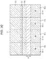
- FIG. 30 is a view for describing arrangement of photodiodes in a pixel array unit.
- FIG. 31 is a view for describing arrangement of photodiodes in a pixel array unit.
- FIG. 32 is a view for describing manufacture of a pixel.
- FIG. 33 is a view for describing manufacture of a pixel.
- FIG. 34 is a view for describing manufacture of a pixel.
- FIG. 35 is a view for describing a configuration of a case of using pixels in combination.
- FIG. 36 is a view for describing a configuration of a case of using pixels in combination.
- FIG. 37 is a view for describing a configuration of a case where photodiodes are stacked in a vertical direction.
- FIG. 38 is a view for describing a configuration of a case where photodiodes are stacked in a vertical direction.
- FIGS. 39 A, 39 B, and 39 C are graphs and views for describing configurations of pixels in a case of using a dot array-type plasmon filter.
- FIGS. 40 A and 40 B are views for describing configurations of pixels in a case of using a square array-type plasmon filter.
- FIGS. 41 A, 41 B, and 41 C are views for describing pixels having a stacked structure.
- FIGS. 42 A, 42 B, and 42 C are views for describing pixels having a stacked structure.
- FIG. 43 is views for describing a stacked structure.
- FIG. 44 is views for describing a stacked structure.
- FIG. 45 is views for describing a stacked structure.
- FIG. 46 is views for describing a stacked structure.
- FIG. 47 is views for describing a stacked structure.
- FIG. 48 is a view for describing a light-shielding structure in a stacked structure.
- FIG. 49 is a view for describing a light-shielding structure in a stacked structure.
- FIG. 50 is a view illustrating a configuration example of a pixel in which a thermal sensor is stacked.
- FIGS. 51 A, 51 B, and 51 C are views for describing a shape of the thermal sensor.
- FIGS. 52 A, 52 B, and 52 C are views illustrating a configuration example of a pixel in which a thermal sensor is stacked.
- FIG. 1 is a block diagram illustrating an embodiment of an imaging device that is a type of electronic devices to which the present technology is applied.
- An imaging device 10 in FIG. 1 is, for example, a digital camera capable of capturing both of a still image and a moving image. Furthermore, the imaging device 10 includes, for example, a multispectral camera capable of detecting light (multispectrum) in four or more wavelength bands (four or more bands) larger than three primary colors or three wavelength bands (three bands) of conventional red (R), green (G), and blue (B), or yellow (Y), magenta (M), and cyan (C) based on a color-matching function.
- a multispectral camera capable of detecting light (multispectrum) in four or more wavelength bands (four or more bands) larger than three primary colors or three wavelength bands (three bands) of conventional red (R), green (G), and blue (B), or yellow (Y), magenta (M), and cyan (C) based on a color-matching function.
- the imaging device 10 includes an optical system 11 , an imaging element 12 , a memory 13 , a signal processing unit 14 , an output unit 15 , and a control unit 16 .
- the optical system 11 includes, for example, a zoom lens, a focus lens, a diaphragm, and the like (not illustrated), and allows external light to enter the imaging element 12 . Furthermore, the optical system 11 is provided with various filters such as a polarizing filter as needed.
- the imaging element 12 includes a complementary metal oxide semiconductor (CMOS) image sensor, for example.
- CMOS complementary metal oxide semiconductor
- the imaging element 12 receives incident light from the optical system 11 , performs photoelectric conversion, and outputs image data corresponding to the incident light.
- CMOS complementary metal oxide semiconductor
- the memory 13 temporarily stores image data output by the imaging element 12 .
- the signal processing unit 14 performs signal processing (for example, processing such as noise removal and white balance adjustment) using the image data stored in the memory 13 and supplies the processed image data to the output unit 15 .
- signal processing for example, processing such as noise removal and white balance adjustment
- the output unit 15 outputs the image data from the signal processing unit 14 .
- the output unit 15 includes a display (not illustrated) configured by a liquid crystal or the like, and displays a spectrum (image) corresponding to the image data from the signal processing unit 14 as a so-called through image.
- the output unit 15 includes a driver (not illustrated) for driving a recording medium such as a semiconductor memory, a magnetic disk, or an optical disk, and records the image data from the signal processing unit 14 on the recording medium.
- the output unit 15 functions as a communication interface that performs communication with an external device (not illustrated), and transmits the image data from the signal processing unit 14 to the external device by wireless or wired means.
- the control unit 16 controls each unit of the imaging device 10 according to a user operation or the like.
- FIG. 2 is a block diagram illustrating a configuration example of a circuit of the imaging element 12 in FIG. 1 .
- the imaging element 12 includes a pixel array unit 31 , a row scanning circuit 32 , a phase locked loop (PLL) 33 , a digital analog converter (DAC) 34 , a column analog digital converter (ADC) circuit 35 , a column scanning circuit 36 , and a sense amplifier 37 .
- PLL phase locked loop
- DAC digital analog converter
- ADC column analog digital converter
- a plurality of pixels 51 is two-dimensionally arrayed.
- Each of the pixels 51 is arranged at a point where a horizontal signal line H connected to the row scanning circuit 32 and a vertical signal line V connected to the column ADC circuit 35 intersect, and includes a photodiode 61 for performing photoelectric conversion and several types of transistors for reading stored signals. That is, the pixel 51 includes a photodiode 61 , a transfer transistor 62 , a floating diffusion 63 , an amplification transistor 64 , a selection transistor 65 , and a reset transistor 66 , as illustrated in an enlarged manner on the right side in FIG. 2 .
- a charge stored in the photodiode 61 is transferred to the floating diffusion 63 via the transfer transistor 62 .
- the floating diffusion 63 is connected to a gate of the amplification transistor 64 .
- the selection transistor 65 is turned on from the row scanning circuit 32 via the horizontal signal line H, and the amplification transistor 64 is source-follower driven, so that the signal of the selected pixel 51 is read out to the vertical signal line V as a pixel signal corresponding to a stored charge amount of the charge stored in the photodiode 61 .
- the pixel signal is reset by turning on the reset transistor 66 .
- the row scanning circuit 32 sequentially outputs, for each row, drive signals for driving (for example, transferring, selecting, resetting, or the like) the pixels 51 of the pixel array unit 31 .
- the PLL 33 generates and outputs a clock signal having a predetermined frequency required for driving each unit of the imaging element 12 on the basis of a clock signal supplied from the outside.
- the DAC 34 generates and outputs a ramp signal having a shape (substantially sawtooth shape) in which a voltage is returned to a predetermined voltage value after dropping at a fixed gradient from the predetermined voltage value.
- the column ADC circuit 35 includes comparators 71 and counters 72 by the number corresponding to columns of the pixels 51 of the pixel array unit 31 , and extracts a signal level by a correlated double sampling (CDS) operation from the pixel signal output from the pixel 51 and outputs pixel data. That is, the comparator 71 compares the ramp signal supplied from the DAC 34 with the pixel signal (luminance value) output from the pixel 51 , and supplies a resultant comparison result signal to the counter 72 . Then, the counter 72 counts the counter clock signal having a predetermined frequency according to the comparison result signal output from the comparator 71 , so that the pixel signal is A/D converted.
- CDS correlated double sampling
- the column scanning circuit 36 sequentially supplies a signal for outputting the pixel data to the counter 72 of the column ADC circuit 35 at predetermined timing.
- the sense amplifier 37 amplifies the pixel data supplied from the column ADC circuit 35 and outputs the amplified pixel data to the outside of the imaging element 12 .
- FIG. 3 schematically illustrates a configuration example of a cross section of the imaging element 12 in FIG. 1 .
- FIG. 3 illustrates a cross section of four pixels 51 - 1 to 51 - 4 of the imaging element 12 .
- the pixels 51 - 1 to 51 - 4 are simply referred to as pixels 51 in a case where there is no necessity to individually distinguish the pixels 51 - 1 to 51 - 4 .
- the imaging element 12 includes a back-illuminated CMOS image sensor in which the photoelectric conversion element layer 105 is arranged on a light incident side with respect to the wiring layer 106 .
- the on-chip microlens 101 is an optical element for condensing light on the photoelectric conversion element layer 105 of each pixel 51 .
- the interlayer films 102 and 104 include a dielectric such as SiO2. As will be described below, dielectric constants of the interlayer films 102 and 104 are desirably as low as possible.
- a narrow band filter NB that is an optical filter that transmits narrow band light in a predetermined narrow wavelength band (narrow band) is provided in each pixel 51 .
- a plasmon filter using surface plasmons which is a type of metal thin film filters using a metal-made thin film such as aluminum, is used as the narrow band filter NB.
- a transmission band of the narrow band filter NB is set for each pixel 51 .
- Types (number of bands) of the transmission band of the narrow band filter NB is arbitrary, and are set to four or more, for example.
- the narrow band refers to, for example, a wavelength band narrower than transmission bands of color filters of the three primary colors or the conventional red (R), green (G), and blue (B), or yellow (Y), magenta (M), and cyan (C), the conventional red (R), green (G), or blue (B) based on a color-matching function.
- a pixel that receives narrow band light transmitted through the narrow band filter NB is referred to as a multispectral pixel or an MS pixel.
- the photoelectric conversion element layer 105 includes the photodiode 61 and the like in FIG. 2 , for example, and receives the light (narrow band light) transmitted through the narrow band filter layer 103 (narrow band filter NB) and converts the received light into charges. Furthermore, the photoelectric conversion element layer 105 is configured such that the pixels 51 are electrically separated by an element separation layer.
- the wiring layer 106 is provided with wiring for reading the charge stored in the photoelectric conversion element layer 105 , and the like.
- a plasmon filter that can be used as the narrow band filter NB will be described with reference to FIGS. 4 , 5 , 6 , 7 , 8 , 9 , 10 A, 10 B, 11 , 12 A, 12 B, 13 , 14 , and 15 .
- FIG. 4 illustrates a configuration example of a plasmon filter 121 A having a hole array structure.
- the plasmon filter 121 A is configured by a plasmon resonator in which holes 132 A are arranged in a honeycomb manner in a metal-made thin film (hereinafter, referred to as a conductive thin film) 131 A.
- Each hole 132 A penetrates the conductive thin film 131 A and functions as a waveguide tube.
- a waveguide tube has a cutoff frequency and a cutoff wavelength determined according to a shape such as a side length and a diameter, and has a property that light having a frequency equal to or lower than the cutoff frequency (a wavelength equal to or larger than the cutoff wavelength) does not propagate.
- the cutoff wavelength of the hole 132 A mainly depends on an opening diameter D 1 , and the cutoff wavelength becomes shorter as the opening diameter D 1 is smaller. Note that the opening diameter D 1 is set to a value smaller than the wavelength of light to be transmitted.
- FIG. 5 is a graph illustrating a dispersion relationship of surface plasmons.
- the horizontal axis of the graph represents an angular wave number vector k, and a vertical axis represents an angular frequency ⁇ .
- ⁇ p represents a plasma frequency of the conductive thin film 131 A.
- ⁇ sp represents a surface plasma frequency at the boundary surface between the interlayer film 102 and the conductive thin film 131 A, and is expressed by the following expression (1).
- ⁇ d represents a dielectric constant of the dielectric configuring the interlayer film 102 .
- the surface plasma frequency ⁇ sp becomes higher as the plasma frequency ⁇ p becomes higher according to the expression (1). Furthermore, the surface plasma frequency ⁇ sp becomes higher as the dielectric constant ⁇ d becomes smaller.
- a line L 1 represents a light dispersion relationship (light line) and is expressed by the following expression (2).
- c represents a light speed
- a line L 2 represents a dispersion relationship of the surface plasmons, and is expressed by the following expression (3).
- ⁇ n represents a dielectric constant of the conductive thin film 131 A.
- the dispersion relationship of the surface plasmons represented by the line L 2 asymptotically approaches the light line represented by the line L 1 in a range where the angular wave number vector k is small, and asymptotically approaches the surface plasma frequency ⁇ sp as the angular wave number vector k becomes large.
- A represents a wavelength of incident light. 6 represents an incidence angle of the incident light.
- G x and G y are expressed by the following expression (5).
- 2 ⁇ / a 0 (5)
- a 0 represents a lattice constant of the hole array structure including the holes 132 A of the conductive thin film 131 A.
- the left side of the expression (4) indicates the angular wave number vector of the surface plasmon
- the right side indicates the angular wave number vector of a hole array period of the conductive thin film 131 A. Therefore, when the angular wave number vector of the surface plasmon becomes equal to the angular wave number vector of the hole array period of the conductive thin film 131 A, the abnormal plasmon transmission phenomenon occurs. Then, the value of ⁇ at this time is a plasmon resonance wavelength (a transmission wavelength of the plasmon filter 121 A).
- the angular wave number vector of the surface plasmon on the left side of the expression (4) is determined according to the dielectric constant ⁇ m of the conductive thin film 131 A and the dielectric constant ⁇ d of the interlayer film 102 .
- the angular wave number vector of the hole array period on the right side is determined according to the incidence angle ⁇ of light and a pitch (hole pitch) P 1 between adjacent holes 132 A of the conductive thin film 131 A. Therefore, the resonance wavelength and a resonance frequency of the plasmon are determined according to the dielectric constant cm of the conductive thin film 131 A, the dielectric constant ⁇ d of the interlayer film 102 , the incidence angle ⁇ of light, and the hole pitch P 1 .
- the resonance wavelength and the resonance frequency of the plasmon are determined according to the dielectric constant ⁇ m of the conductive thin film 131 A, the dielectric constant ⁇ d of the interlayer film 102 , and the hole pitch P 1 .
- a transmission band (plasmon resonance wavelength) of the plasmon filter 121 A changes depending on the material and film thickness of the conductive thin film 131 A, the material and film thickness of the interlayer film 102 , and a hole array pattern period (for example, the opening diameter D 1 and the hole pitch P 1 of the hole 132 A), and the like.
- the transmission band of the plasmon filter 121 A changes depending on the hole array pattern period, particularly, the hole pitch P 1 . That is, the transmission band of the plasmon filter 121 A shifts to a shorter wavelength side as the hole pitch P 1 becomes narrower, and the transmission band of the plasmon filter 121 A shifts to a longer wavelength side as the hole pitch P 1 becomes wider.
- FIG. 6 is a graph illustrating an example of spectral characteristics of the plasmon filter 121 A in a case where the hole pitch P 1 is changed.
- the horizontal axis of the graph represents the wavelength (the unit is nm), and the vertical axis represents sensitivity (the unit is arbitrary unit).
- a line L 11 represents a spectral characteristic in a case where the hole pitch P 1 is set to 250 nm
- a line L 12 represents a spectral characteristic in a case where the hole pitch P 1 is set to 325 nm
- a line L 13 represents a spectral characteristic in a case where the hole pitch P 1 is set to 500 nm.
- the plasmon filter 121 A mainly transmits light in a blue wavelength band. In the case where the hole pitch P 1 is set to 325 nm, the plasmon filter 121 A mainly transmits light in a green wavelength band. In the case where the hole pitch P 1 is set to 500 nm, the plasmon filter 121 A mainly transmits light in a red wavelength band. Note that, in the case where the hole pitch P 1 is set to 500 nm, the plasmon filter 121 A also transmits light in a lower wavelength band than red according to a waveguide mode to be described below.
- FIG. 7 is a graph illustrating another example of spectral characteristics of the plasmon filter 121 A in a case where the hole pitch P 1 is changed.
- the horizontal axis of the graph represents the wavelength (the unit is nm), and the vertical axis represents sensitivity (the unit is arbitrary unit).
- This example illustrates an example of spectral characteristics of sixteen types of plasmon filters 121 A in a case where the hole pitch P 1 is changed at intervals of 25 nm from 250 nm to 625 nm.
- transmittance of the plasmon filter 121 A is mainly determined according to the opening diameter D 1 of the hole 132 A.
- the transmittance becomes higher while the color mixture is more likely to occur as the opening diameter D 1 becomes larger.
- each hole 132 A of the plasmon filter 121 A functions as a waveguide tube, as described above. Therefore, in the spectral characteristics, there are some cases where not only a wavelength component transmitted by surface plasmon resonance (a wavelength component in a plasmon mode) but also a wavelength component transmitted through the hole 132 A (waveguide tube) (a wavelength component in a waveguide mode) becomes large, depending on a pattern of the hole array of the plasmon filter 121 A.
- FIG. 8 illustrates spectral characteristics of the plasmon filter 121 A in a case where the hole pitch P 1 is set to 500 nm, similarly to the spectral characteristics represented by the line L 13 in FIG. 6 .
- a longer wavelength side than the cutoff wavelength around 630 nm is a wavelength component in the plasmon mode, and a shorter wavelength side than the cutoff wavelength is a waveguide component in the waveguide mode.
- the cutoff wavelength mainly depends on the opening diameter D 1 of the hole 132 A, and the cutoff wavelength becomes shorter as the opening diameter D 1 is smaller. Then, wavelength resolution characteristics of the plasmon filter 121 A are improved as a difference between the cutoff wavelength and a peak wavelength in the plasmon mode is made larger.
- the surface plasma frequency ⁇ sp of the conductive thin film 131 A becomes higher as the plasma frequency ⁇ p of the conductive thin film 131 A becomes higher. Furthermore, the surface plasma frequency ⁇ sp becomes higher as the dielectric constant ⁇ d of the interlayer film 102 becomes smaller. Then, the plasmon resonance frequency can be set to be higher as the surface plasma frequency ⁇ sp becomes higher, and the transmission band (plasmon resonance wavelength) of the plasmon filter 121 A can be set to a shorter wavelength band.
- a metal having a smaller plasma frequency ⁇ p for the conductive thin film 131 A enables setting of a shorter wavelength band as the transmission band of the plasmon filter 121 A.
- a metal having a smaller plasma frequency ⁇ p for the conductive thin film 131 A enables setting of a shorter wavelength band as the transmission band of the plasmon filter 121 A.
- aluminum, silver, gold, or the like is suitable.
- copper or the like can be used in a case where the transmission band is set to a long wavelength band such as infrared light.
- a dielectric having a smaller dielectric constant ⁇ d for the interlayer film 102 enables setting of a shorter wavelength band as the transmission band of the plasmon filter 121 A.
- a dielectric having a smaller dielectric constant ⁇ d for the interlayer film 102 enables setting of a shorter wavelength band as the transmission band of the plasmon filter 121 A.
- SiO2, SiN, Low-K, SiC, TiO2, ZnS, MgF2, or the like is suitable.
- FIG. 9 is a graph illustrating propagation characteristics of the surface plasmons at an interface between the conductive thin film 131 A and the interlayer film 102 in a case where aluminum is used for the conductive thin film 131 A and SiO2 is used for the interlayer film 102 .
- the horizontal axis of the graph represents the wavelength (the unit is nm), and the vertical axis represents a propagation distance (the unit is ⁇ m).
- a line L 21 represents a propagation characteristic in an interface direction
- a line L 22 represents a propagation characteristic in a depth direction of the interlayer film 102 (a direction perpendicular to the interface)
- a line L 23 represents a propagation characteristic in the depth direction of the conductive thin film 131 A (the direction perpendicular to the interface).
- a propagation distance ⁇ SPP (A) of the surface plasmon in the depth direction is expressed by the following expression (6).
- k SPP represents an absorption coefficient of a substance through which the surface plasmon propagates.
- ⁇ m ( ⁇ ) represents the dielectric constant of the conductive thin film 131 A with respect to light having a wavelength ⁇ .
- ⁇ d ( ⁇ ) represents the dielectric constant of the interlayer film 102 with respect to the light having the wavelength ⁇ .
- the surface plasmon with respect to the light having the wavelength of 400 nm propagates from the surface of the interlayer film 102 containing SiO2 to about 100 nm in the depth direction. Therefore, by setting the thickness of the interlayer film 102 to 100 nm or more, an influence of a substance stacked on a surface of the interlayer film 102 , the surface being opposite to the conductive thin film 131 A, on the surface plasmons at the interface between the interlayer film 102 and the conductive thin film 131 A can be prevented.
- the surface plasmon with respect to the light having the wavelength of 400 nm propagates from the surface of the conductive thin film 131 A containing aluminum to about 10 nm in the depth direction. Therefore, by setting the thickness of the conductive thin film 131 A to 10 nm or more, an influence of the interlayer film 104 on the surface plasmons at the interface between the interlayer film 102 and the conductive thin film 131 A can be prevented.
- FIGS. 10 A, 10 B, 11 , 12 A, 12 B, 13 , 14 , and 15 will be described with reference to FIGS. 10 A, 10 B, 11 , 12 A, 12 B, 13 , 14 , and 15 .
- a plasmon filter 121 B in FIG. 10 A is configured by a plasmon resonator in which holes 132 B are arranged in an orthogonal matrix in a conductive thin film 131 B.
- the transmission band changes depending on a pitch P 2 between adjacent holes 132 B, for example.
- the plasmon resonator not all the holes need to penetrate the conductive thin film. Even if some holes are configured as non-through holes that do not penetrate the conductive thin film, the plasmon resonator functions as a filter.
- FIG. 10 B illustrates a plan view and a cross-sectional view (taken along line A-A′ in the plan view) of a plasmon filter 121 C configured by a plasmon resonator in which holes 132 C configured as through holes and holes 132 C′ configured as non-through holes are arranged in a honeycomb manner in a conductive thin film 131 C. That is, the holes 132 C configured as through holes and the holes 132 C′ configured as non-through holes are periodically arranged in the plasmon filter 121 C.
- the plasmon filter may be configured by a two-layer plasmon resonator, for example.
- a plasmon filter 121 D illustrated in FIG. 11 includes a two-layer plasmon filter 121 D- 1 and plasmon filter 121 D- 2 .
- the plasmon filter 121 D- 1 and the plasmon filter 121 D- 2 have a structure in which holes are arranged in a honeycomb manner, similarly to the plasmon resonator configuring the plasmon filter 121 A in FIG. 4 .
- a distance D 2 between the plasmon filter 121 D- 1 and the plasmon filter 121 D- 2 is favorably set to about 1 ⁇ 4 of a peak wavelength of the transmission band. Furthermore, the distance D 2 is more favorably equal to or less than 1 ⁇ 2 of the peak wavelength of the transmission band in consideration of the degree of freedom in design.
- the holes may be arranged in patterns similar to each other in a two-layer plasmon resonator structure, for example, other than the structure like the plasmon filter 121 D in which the holes are arranged in the same pattern in the plasmon filter 121 D- 1 and the plasmon filter 121 D- 2 .
- holes and dots may be arranged in a pattern in which a hole array structure and a dot array structure (to be described below) are inverted in the two-layer plasmon resonator structure.
- a three or more multilayer structure can be adopted although the plasmon filter 121 D has the two-layer structure.
- the configuration example of the plasmon filter using the plasmon resonator having the hole array structure has been described.
- a plasmon resonator having a dot array structure may be adopted as the plasmon filter.
- a plasmon filter having a dot array structure will be described with reference to FIGS. 12 A and 12 B .
- a plasmon filter 121 A′ in FIG. 12 A has a negative-positive inverted structure with respect to the plasmon resonator of the plasmon filter 121 A in FIG. 4 , that is, configured by a plasmon resonator in which dots 133 A are arranged in a honeycomb manner in a dielectric layer 134 A.
- the dielectric layer 134 A is added between the dots 133 A.
- the plasmon filter 121 A′ is used as a complementary color filter to absorb light in a predetermined wavelength band.
- the wavelength band (hereinafter referred to as absorption band) of light absorbed by the plasmon filter 121 A′ changes depending on a pitch between adjacent dots 133 A (hereinafter referred to as a dot pitch) P 3 , or the like. Furthermore, a diameter D 3 of the dot 133 A is adjusted according to the dot pitch P 3 .
- a plasmon filter 121 B′ in FIG. 12 B has a negative-positive inverted structure with respect to the plasmon resonator of the plasmon filter 121 B in FIG. 10 A , that is, a plasmon resonator structure in which dots 133 B are arranged in a straight matrix in a dielectric layer 134 B.
- the dielectric layer 134 B is added between the dots 133 B.
- the absorption band of the plasmon filter 121 B′ changes depending on a dot pitch P 4 between adjacent dots 133 B, or the like. Furthermore, a diameter D 3 of the dot 133 B is adjusted according to the dot pitch P 4 .
- FIG. 13 is a graph illustrating an example of spectral characteristics in a case where the dot pitch P 3 of the plasmon filter 121 A′ in FIG. 12 A is changed.
- the horizontal axis of the graph represents the wavelength (the unit is nm), and the vertical axis represents the transmittance.
- a line L 31 represents a spectral characteristic in a case where the dot pitch P 3 is set to 300 nm
- a line L 32 represents a spectral characteristic in a case where the dot pitch P 3 is set to 400 nm
- a line L 33 represents a spectral characteristic in a case where the dot pitch P 3 is set to 500 nm.
- the absorption band of the plasmon filter 121 A′ shifts to a shorter wavelength side as the dot pitch P 3 becomes narrower, and the absorption band of the plasmon filter 121 A′ shifts to a longer wavelength side as the dot pitch P 3 becomes wider.
- the transmission band or the absorption band can be adjusted by simply adjusting the pitch in a planar direction of the holes or dots. Therefore, for example, the transmission band or the absorption band can be individually set for each pixel by simply adjusting the pitch of holes or dots in a lithography process, and multi-coloring of the filter can be implemented with fewer steps.
- the thickness of the plasmon filter is about 100 to 500 nm, which is nearly similar to an organic material-based color filter, and process affinity is good.
- a plasmon filter 151 using guided mode resonant (GMR) illustrated in FIG. 14 can be used as the narrow band filter NB.
- GMR guided mode resonant
- a conductive layer 161 , a SiO2 film 162 , a SiN film 163 , and a SiO2 substrate 164 are stacked in order from the top.
- the conductive layer 161 is included in, for example, the narrow band filter layer 103 in FIG. 3
- the SiO2 film 162 , the SiN film 163 , and the SiO2 substrate 164 are included in, for example, the interlayer film 104 in FIG. 3 .
- rectangular conductive thin films 161 A containing, for example, aluminum are arranged at a predetermined pitch P 5 in such a manner that long sides of the conductive thin films 161 A are adjacent to each other. Then, the transmission band of the plasmon filter 151 changes depending on the pitch P 5 or the like.
- FIG. 15 is a graph illustrating an example of spectral characteristics of the plasmon filter 151 in a case where the hole pitch P 5 is changed.
- the horizontal axis of the graph represents the wavelength (the unit is nm), and the vertical axis represents the transmittance.
- This example illustrates an example of spectral characteristics in a case where the pitch P 5 is changed into six types at intervals of 40 nm from 280 nm to 480 nm, and a slit width between the adjacent conductive thin films 161 A is set to 1 ⁇ 4 of the pitch P 5 .
- a waveform having the shortest peak wavelength of the transmission band represents the spectral characteristic of the case where the pitch P 5 is set to 280 nm, and the peak wavelength becomes longer as the pitch P 5 becomes wider. That is, the transmission band of the plasmon filter 151 shifts to a shorter wavelength side as the pitch P 5 becomes narrower, and the transmission band of the plasmon filter 151 shifts to a longer wavelength side as the pitch P 5 becomes wider.
- the plasmon filter 151 using GMR also has good affinity for an organic material-based color filter, similarly to the above-described plasmon filters having the hole array structure and the dot array structure.
- a filter having a shape called a bull's eye (hereinafter, referred to as a bullseye structure) can be applied, other than the hole array structure, the dot array structure, and the structure using GMR.
- the bullseye structure is a name given because the structure resembles a dart target or a bow and arrow target.
- a plasmon filter 171 having the bullseye structure has a through hole 181 in the center, and includes a plurality of protrusions 182 concentrically formed around the through hole 181 . That is, the plasmon filter 171 having the bullseye structure has a shape to which a metal diffraction grating structure that causes plasmon resonance is applied.
- the plasmon filter 171 having the bullseye structure has similar characteristics to the plasmon filter 151 using GMR. That is, in a case where the distance between the protrusions 182 is a pitch P 6 , the transmission band of the plasmon filter 171 shifts to a shorter wavelength side as the pitch P 6 becomes narrower, and the transmission band of the plasmon filter 171 shifts to a longer wavelength side as the pitch P 6 becomes wider.
- a Fabry-Perot interferometer As a filter that transmits light of a specific wavelength, there is a Fabry-Perot interferometer.
- a Fabry-Perot interferometer can be used as the narrow band filter to which the present technology is applied, instead of a plasmon filter.
- a Fabry-Perot interferometer 201 is an optical device including two semi-transparent mirrors 202 and 203 , and having the two semi-transparent mirrors 202 and 203 arranged to face each other in parallel, as illustrated in FIG. 17 .
- the semi-transparent mirrors 202 and 203 are finished with a reflective surface having high reflectance and slight transmittance.
- Light incident on one side of the Fabry-Perot interferometers 201 (upper side in FIG. 17 ) reflects and reciprocates between the two reflective surfaces many times and interferes with each other.
- the light transmitted through the semi-transparent mirror 203 becomes interference light having a considerable length due to the light that has reciprocated many times with a certain optical path difference. Therefore, if the Fabry-Perot interferometer 201 is used as a spectroscope, a very high resolution can be obtained.
- a wavelength to be analyzed by the Fabry-Perot interferometer 201 of the incident light, can be selected by the Fabry-Perot interferometer 201 , and the selected light can be received by the photodiode 61 , similarly to the above-described plasmon filter 121 ( 151 ).
- the examples of the narrow band filter NB applicable to an imaging device to which the present technology is applied include the above-described plasmon filters having, for example, the hole array structure, the dot array structure, the GMR, and the bullseye structure, and the Fabry-Perot interferometer.
- the narrow band filter NB is the plasmon filter 121 having the hole array structure unless otherwise specified.
- the plasmon filter having, for example, the dot array structure, the GMR, or the bullseye structure, or the Fabry-Perot interferometer can be applied, and the description will be continued on the assumption that the plasmon filter 121 can be appropriately replaced with the plasmon filter having, for example, the dot array structure, the GMR, or the bullseye structure, or the Fabry-Perot interferometer.
- the interlayer film 102 , the plasmon filter 121 , the interlayer film 104 , and the photodiode 61 are stacked in order from the top.
- the plasmon filter 121 configures the narrow band filter layer 103 in FIG. 3
- the photodiode 61 represents one photoelectric conversion element included in the photoelectric conversion element layer 105 .
- the photodiode 61 includes a P-type semiconductor region 61 - 1 and an N-type semiconductor region 61 - 2 . Note that the P-type semiconductor region 61 - 1 may be formed to surround the N-type semiconductor region 61 - 2 although not illustrated in FIG. 18 . The P-type semiconductor region 61 - 1 also serves as a hole charge storage region for suppressing dark current.
- the N-type semiconductor region 61 - 2 is a region of a main part of the photodiode 61 , and a read charge is an electron, as an example.
- the present technology can be applied to a photodiode in which the region of a main part of the photodiode 61 is the P-type semiconductor region, and the read charge is a hole.
- FIG. 19 A spectral characteristic example of when the pixel 51 illustrated in FIG. 18 has received light is illustrated in FIG. 19 .
- the horizontal axis represents the wavelength of the incident light
- the vertical axis represents an output value.
- a graph having a peak at 600 nm is obtained as a graph of spectral characteristics, as illustrated as the graph in FIG. 19 . It is favorable if the graph is diverged centered on the peak value. However, as illustrated in FIG. 19 , occurrence of a color mixture component is read on the wavelength side shorter than 600 nm.
- a portion surrounded by the circle indicates a portion where the color mixture component has occurred.
- This color mixture component tends to more easily occur when the wavelength set as the wavelength of light to be transmitted through the plasmon filter 121 is on a long wavelength side. Since such a color mixture component becomes a cause of deterioration of the spectral characteristics, it is favorable to suppress the occurrence.
- the pixel 51 capable of suppressing the color mixture component will be described.
- FIGS. 20 A, 20 B, 20 C, and 20 D are graphs and views illustrating configurations of an embodiment of the pixels 51 to which the present technology is applied.
- a pixel 51 a illustrated in FIGS. 20 A, 20 B, 20 C, and 20 D has the photodiode 61 formed at a depth appropriate for the wavelength of light transmitted through the plasmon filter 121 .
- FIGS. 20 A, 20 B, 20 C, and 20 D Graphs of spectral characteristics of the plasmon filters 121 are illustrated in the upper part in FIGS. 20 A, 20 B, 20 C, and 20 D , and the configurations of the pixels 51 of when the graphs of the spectral characteristics are obtained, that is, the configurations of the pixels 51 to which the present technology is applied, are illustrated in the lower part in FIGS. 20 A, 20 B, 20 C, and 20 D .
- the configurations of the pixels 51 illustrated in the lower part in FIGS. 20 A, 20 B, 20 C, and 20 D are the same as the configuration of the pixel 51 illustrated in FIG. 18 , but depths of the photodiodes 61 (the N-type semiconductor regions 61 - 2 configuring the photodiodes 61 ) are different.
- the “depth of the photodiode 61 ” refers to the depth of the N-type semiconductor region 61 - 2 configuring the photodiode 61 . Furthermore, the “depth of the photodiode 61 ” refers to a distance from an interface of the silicon substrate on which the photodiode 61 is formed (a boundary with respect to the interlayer film 104 ) to a position where a depletion layer spreads, and a region where the depletion layer spreads is the N-type semiconductor region 61 - 2 .
- the depth of the photodiode 61 can be the distance from the interface of the silicon substrate to the position where the depletion layer spreads, and can be the distance to the depletion layer, in this case, to the interface (upper end) of the N-type semiconductor region 61 - 2 or may be the distance to a center portion of the N-type semiconductor region 61 - 2 .
- the description will be continued using the distance to the interface of the N-type semiconductor region 61 - 2 .
- the N-type semiconductor region is a region of a main part of photoelectric conversion.
- the P-type semiconductor region is a region of a main part of photoelectric conversion.
- the present technology can be applied by appropriately replacing the N-type semiconductor region with the P-type semiconductor region in the above and the following description.
- the description will be continuously given by taking an example in which the depth of the photodiode 61 is a physical depth.
- a method of changing the depth of the photodiode 61 it is also possible to perform channel cut or change the depth of a p+ region on the surface (impurity concentration profile) or change the depth of a well (impurity concentration profile).
- the depth of the photodiode 61 may be changed by such a method.
- FIGS. 20 A, 20 B, 20 C, and 20 D description will be continued using the case of the hole array-type plasmon filter 121 as an example.
- the dot array-type plasmon filter 121 the plasmon filter 151 using GMR, the plasmon filter 171 having the bullseye structure, or the Fabry-Perot interferometer 201 can be used instead of the hole array-type plasmon filter 121 .
- the present technology can be applied similarly to the case of using the hole array-type plasmon filter 121 .
- FIG. 20 A illustrates a configuration of the pixel 51 a in a case of using a plasmon filter 121 a in which the wavelength of light transmitted through the plasmon filter 121 a is set to 450 nm.
- a photodiode 61 a is formed at a position of a depth d 1 .
- FIG. 20 B illustrates a configuration of a pixel 51 b in a case of using a plasmon filter 121 b in which the wavelength of light transmitted through the plasmon filter 121 b is set to 530 nm.
- a photodiode 61 b is formed at a position of a depth d 2 .
- FIG. 20 C illustrates a configuration of a pixel 51 c in a case of using a plasmon filter 121 c in which the wavelength of light transmitted through the plasmon filter 121 c is set to 600 nm.
- a photodiode 61 c is formed at a position of a depth d 3 .
- FIG. 20 D illustrates a configuration of a pixel 51 d in a case of using a plasmon filter 121 d in which the wavelength of light transmitted through the plasmon filter 121 d is set to 650 nm.
- a photodiode 61 d is formed at a position of a depth d 4 .
- the depths at which the photodiodes 61 are formed are different.
- the depths of the pixels 51 a to 51 d are the depth d 1 , the depth d 2 , the depth d 3 , and the depth d 4 , respectively.
- the depths d 1 to d 4 satisfy the relationship of the depth d 1 ⁇ the depth d 2 ⁇ the depth d 3 ⁇ the depth d 4 .
- the plasmon filters 121 a to 121 d are filters designed to most efficiently transmit the light having the wavelengths of 450 nm, 530 nm, 600 nm, and 650 nm, respectively. That is, the wavelength of the transmitted light shifts to a longer wavelength side in the order of the plasmon filter 121 a , the plasmon filter 121 b , the plasmon filter 121 c , and the plasmon filter 121 d.
- the depth of the photodiode 61 becomes deeper.
- the photodiode 61 is formed at the depth appropriate for the wavelength of light transmitted through the plasmon filter 121 .
- the photodiode 61 is formed on a silicon substrate. It is generally known that light having a longer wavelength and having entered a silicon substrate reaches a deeper position in the silicon substrate. Since, by using such a fact, the photodiode 61 is formed at the position that the light having the wavelength transmitted through the plasmon filter 121 reaches in the silicon substrate, the position where the photodiode 61 is formed is different according to the wavelength of the light transmitted through the plasmon filter 121 .
- the depth of the photodiode 61 will be further described.
- light intensity I at a depth x from the surface becomes
- I I 0 e ⁇ x .
- I 0 represents the light intensity on the substance surface
- ⁇ represents the absorption coefficient.
- the light is absorbed on the substance surface as the absorption coefficient ⁇ is larger, and the light penetrates the substance into a deeper position as the absorption coefficient ⁇ is smaller.
- FIG. 21 illustrates a relationship between the absorption coefficient ⁇ of single crystal silicon and the wavelength of light.
- the horizontal axis of the graph illustrated in FIG. 21 represents the wavelength of light, and the vertical axis represents the absorption coefficient ⁇ . It can be read from the graph in FIG. 21 that the absorption coefficient ⁇ changes according to the wavelength of light entering the single crystal silicon and is not constant. That is, it is understood that the absorption coefficient ⁇ greatly depends on the substance and the wavelength of the incident light.
- FIG. 22 illustrates a relationship between the light intensity and the penetration depth in the single crystal silicon.
- the horizontal axis of the graph illustrated in FIG. 22 represents the depth that light penetrates and the vertical axis represents the light intensity.
- the sensitivity can be improved by forming the photodiode 61 on the silicon surface in the case of using the plasmon filter 121 that transmits the blue light. Meanwhile, when the photodiode 61 is formed at a deep position of the silicon, for example, at a position deeper than 0.3 um, the intensity becomes weak before the blue light reaches the photodiode 61 , and the blue light reaching the photodiode 61 is reduced and the sensitivity decreases.
- the photodiode 61 when the photodiode 61 is formed at a position suitable for the wavelength of light transmitted through the plasmon filter 121 , the light can be efficiently received. However, when the photodiode 61 is formed at a position not suitable for the wavelength of light transmitted through the plasmon filter 121 , the light cannot be efficiently received.
- the color mixture component can be reduced.
- the depth of the photodiode 61 is set in consideration of the above points. An example of a way of setting the depth of the photodiode 61 will be described.
- the light to be cut can be, for example, light that may be detected as a color mixture component.
- ⁇ cutoff (a peak transmission wavelength of the plasmon filter) ⁇ (a target half width of the plasmon filter/2)
- FIG. 23 An example of a result of such calculation is illustrated in FIG. 23 .
- the horizontal axis of the graph illustrated in FIG. 23 represents the wavelength, and the vertical axis represents the depth (the upper end position) of the photodiode 61 at which the light intensity becomes 50%.
- Such a graph is created, and the upper end depth of the photodiode 61 can be set on the basis of the graph.
- the depth d 1 of the pixel 51 a , the depth d 2 of the pixel 51 b , the depth d 3 of the pixel 51 c , and the depth d 4 of the pixel 51 d are respectively set to the depths in accordance with the respective transmission wavelengths of the plasmon filters 121 a to 121 d , for example, using the graph illustrated in FIG. 23 .
- the depth of the photodiode 61 becomes deeper, and the configurations of the pixels 51 a to 51 d illustrated in FIGS. 20 A 20 B, 20 C, and 20 D are obtained.
- the pitch of the holes 132 and the depth of the photodiode 61 have the relationship as illustrated in FIGS. 24 A, 24 B, 24 C, and 24 D .
- FIGS. 24 A, 24 B, 24 C, and 24 D are views of when the plasmon filter 121 is viewed from an upper surface (light incident side), and the lower views illustrate configurations of pixels 51 , as in the lower views in FIGS. 20 A, 20 B, 20 C , and 20 D.
- FIG. 24 A illustrates a configuration of the pixel 51 a in a case of using a plasmon filter 121 a in which the pitch of the plasmon filter 121 a is set to 250 nm.
- a photodiode 61 a is formed at a position of a depth d 1 .
- FIG. 24 B illustrates a configuration of the pixel 51 b in a case of using a plasmon filter 121 b in which the pitch of the plasmon filter 121 b is set to 350 nm.
- a photodiode 61 b is formed at a position of a depth d 2 .
- FIG. 24 C illustrates a configuration of the pixel 51 c in a case of using a plasmon filter 121 c in which the pitch of the plasmon filter 121 c is set to 450 nm.
- a photodiode 61 c is formed at a position of a depth d 3 .
- FIG. 24 D illustrates a configuration of the pixel 51 d in a case of using a plasmon filter 121 d in which the pitch of the plasmon filter 121 d is set to 550 nm.
- a photodiode 61 d is formed at a position of a depth d 4 .
- the transmission wavelength becomes longer as the pitch of the holes 132 is larger.
- the plasmon filter 121 a functions as a filter that mainly transmits light of the blue wavelength band.
- the plasmon filter 121 d functions as a filter that mainly transmits light of the red wavelength band.
- the transmission wavelength changes when the interval (pitch) of the holes 132 is changed. Therefore, the photodiode 61 is formed at a depth at which the transmission wavelength is most absorbed by silicon. Furthermore, as a characteristic of the plasmon filter 121 , the transmission wavelength shifts to the longer wavelength side as the interval (pitch) of the holes 132 is made longer. Therefore, the photodiode 61 in the silicon substrate is formed to increase the depth in accordance with such a characteristic.
- the dot array-type plasmon filter 121 can be applied.
- the dot array-type plasmon filter 121 is a filter that absorbs light having a predetermined wavelength band and is used as a complementary color filter, as described with reference to FIGS. 12 A, 12 B, and 13 .
- the wavelength band of light absorbed by the dot array-type plasmon filter 121 changes depending on the pitch between adjacent dots 133 or the like.
- the absorption band of the plasmon filter 121 shifts to a shorter wavelength side as the dot pitch between the dots 133 becomes narrower, and the absorption band of the plasmon filter 121 shifts to a longer wavelength side as the pitch between the dots 133 becomes wider.
- the dot array-type plasmon filter 121 is a filter that absorbs light having a predetermined wavelength band
- the photodiode 61 may be formed in a region having a depth other than the depth in accordance with the predetermined wavelength band, instead of being formed at the depth in accordance with the predetermined wavelength band.
- the pixel 51 in this case will be described below.
- the interval of the conductive thin film 161 (hereinafter described as slit interval) and the depth of the photodiode 61 have the relationship as illustrated in FIGS. 25 A 25 B, 25 C, and 25 D.
- FIGS. 25 A, 25 B, 25 C, and 25 D are views of when the plasmon filter 151 is viewed from an upper surface (light incident side), and the lower views illustrate configurations of pixels 51 , as in the lower views in FIGS. 20 A, 20 B, 20 C , and 20 D.
- FIG. 25 A illustrates a configuration of the pixel 51 a in a case of using a plasmon filter 151 a in which the slit interval of the plasmon filter 151 a is set to 250 nm.
- a photodiode 61 a is formed at a position of a depth d 1 .
- FIG. 25 B illustrates a configuration of the pixel 51 b in a case of using a plasmon filter 151 b in which the slit interval of the plasmon filter 151 b is set to 300 nm.
- a photodiode 61 b is formed at a position of a depth d 2 .
- FIG. 25 C illustrates a configuration of the pixel 51 c in a case of using a plasmon filter 151 c in which the slit interval of the plasmon filter 151 c is set to 350 nm.
- a photodiode 61 c is formed at a position of a depth d 3 .
- FIG. 25 D illustrates a configuration of the pixel 51 d in a case of using a plasmon filter 151 d in which the slit interval of the plasmon filter 151 d is set to 400 nm.
- a photodiode 61 d is formed at a position of a depth d 4 .
- the transmission wavelength becomes longer as the slit interval of the conductive thin film 161 is larger.
- the plasmon filter 151 a functions as a filter that mainly transmits light of the blue wavelength band.
- the plasmon filter 151 d functions as a filter that mainly transmits light of the red wavelength band.
- the transmission wavelength changes when the interval (slit interval) of the conductive thin film 161 is changed. Therefore, the photodiode 61 is formed at a depth at which the transmission wavelength is most absorbed by silicon. Furthermore, as a characteristic of the plasmon filter 151 , the transmission wavelength shifts to the longer wavelength side as the interval (slit interval) of the conductive thin film 161 is made longer. Therefore, the photodiode 61 in the silicon substrate is formed to increase the depth in accordance with such a characteristic.
- the plasmon filter 171 having the bullseye structure illustrated in FIGS. 16 A and 16 B can be used instead of the plasmon filter 121 or the plasmon filter 151 described above.
- a filter using plasmon resonance can be used, and a filter other than the above-described filters can be applied as long as the filter uses plasmon resonance.
- the Fabry-Perot interferometer 201 that transmits light in a predetermined frequency band can be applied as the narrow band filter. That is, a wavelength selection filter can be applied to the present technology, and a filter (interferometer) called Fabry-Perot or etalon can be applied.
- a filter interferometer
- description of a Fabry-Perot filter will be used as an example (collective term) of these wavelength selection filters.
- the Fabry-Perot interferometer 201 is an optical device in which two semi-transparent mirrors 202 and 203 are arranged to face each other in parallel, and is a device that causes lights to reflect and reciprocate between the two reflective surfaces many times and interfere with each other to output interference light of light having a predetermined wavelength.
- the light split by the Fabry-Perot interferometer 201 and output and the depth of the photodiode 61 have the relationship illustrated in FIGS. 26 A, 26 B, 26 C, and 26 D .
- FIGS. 26 A, 26 B, 26 C, and 26 D Graphs of spectral characteristics of the Fabry-Perot interferometers 201 are illustrated in the upper part in FIGS. 26 A, 26 B, 26 C, and 26 D , and the configurations of the pixels 51 of when such graphs of spectral characteristics are obtained, that is, the configurations of the pixels 51 to which the present technology is applied, are illustrated in the lower part in FIGS. 26 A, 26 B, 26 C, and 26 D .
- a selected wavelength is different depending on the interval between the two semi-transparent mirrors 202 and 203 , the refractive index of the substance added between the two semi-transparent mirrors 202 and 203 , and the like, and thus the same thickness (shape) is illustrated in the lower part in FIGS. 26 A, 26 B, 26 C, and 26 D .
- FIG. 26 A illustrates a configuration of the pixel 51 a in a case of using a Fabry-Perot interferometer 201 a in which 450 nm is set as the wavelength of light selected by the Fabry-Perot interferometer 201 a .
- a photodiode 61 a is formed at a position of a depth d 1 .
- FIG. 26 B illustrates a configuration of the pixel 51 b in a case of using a Fabry-Perot interferometer 201 b in which 530 nm is set as the wavelength of light selected by the Fabry-Perot interferometer 201 b .
- a photodiode 61 b is formed at a position of a depth d 2 .
- FIG. 26 C illustrates a configuration of the pixel 51 c in a case of using a Fabry-Perot interferometer 201 c in which 600 nm is set as the wavelength of light selected by the Fabry-Perot interferometer 201 c .
- a photodiode 61 c is formed at a position of a depth d 3 .
- FIG. 26 D illustrates a configuration of the pixel 51 d in a case of using a Fabry-Perot interferometer 201 d in which 650 nm is set as the wavelength of light selected by the Fabry-Perot interferometer 201 d .
- a photodiode 61 d is formed at a position of a depth d 4 .
- the depths at which the photodiodes 61 are formed are different.
- the depths of the pixels 51 a to 51 d are the depth d 1 , the depth d 2 , the depth d 3 , and the depth d 4 , respectively.
- the depths d 1 to d 4 satisfy the relationship of the depth d 1 ⁇ the depth d 2 ⁇ the depth d 3 ⁇ the depth d 4 .
- the Fabry-Perot interferometers 201 a to 121 d are filters designed to most efficiently transmit the light having the wavelengths of 450 nm, 530 nm, 600 nm, and 650 nm, respectively. That is, the wavelength of the transmitted light shifts to a longer wavelength side in the order of the Fabry-Perot interferometer 201 a , the Fabry-Perot interferometer 201 b , the Fabry-Perot interferometer 201 c , and the Fabry-Perot interferometer 201 d.
- the depth of the photodiode 61 becomes deeper.
- the photodiode 61 is formed at the depth appropriate for the wavelength of light transmitted through the plasmon filter 121 .
- the photodiode 61 is formed at the depth where silicon most absorbs the wavelength selected by the Fabry-Perot interferometer 201 .
- the photodiode 61 is formed at the depth at which the photodiode 61 can efficiently receive the light filtered by the narrow band filter.
- the photodiode 61 d of the pixel 51 d is formed at the deep position in the silicon substrate, there is a region where the photodiode 61 is not formed from the photodiode 61 d to the interface of the silicon substrate.
- a drain region for discharging charges may be formed in the pixel 51 .
- the pixels 51 a to 51 d illustrated in FIGS. 27 A, 27 B, 27 C, and 27 D have similar configurations to the pixels 51 a to 51 d illustrated in the lower views in FIGS. 20 A 20 B, 20 C, and 20 D, and the photodiodes 61 a to 61 d are formed at the positions of the depths d 1 to d 4 , respectively.
- a drain 301 b is formed above the region where the photodiode 61 b is formed in the silicon substrate and near the interface of the silicon substrate.
- the drain 301 b is an N-type diffusion layer.
- a P-type semiconductor region 61 - 1 b is formed below the drain 301 b that is the N-type diffusion layer, and the N-type semiconductor region 61 - 2 (photodiode 61 b ) is formed below the P-type semiconductor region 61 - 1 b.
- the drain 301 b is a P-type diffusion layer.
- the description will be continued using the case of the drain 301 that is an N-type diffusion layer as an example.
- the configuration in which the P-type semiconductor region 61 - 1 is formed below the drain 301 that is the N-type diffusion layer, and the N-type semiconductor region 61 - 2 (photodiode 61 ) is formed below the P-type semiconductor region 61 - 1 is similar in the description below. Therefore, description will be appropriately omitted.
- a drain 301 c is formed above the region where the photodiode 61 c is formed in the silicon substrate and near the interface of the silicon substrate.
- the drain 301 c is formed larger than the drain 301 b .
- the drain 301 may be formed in the silicon substrate to have a size similar to the region where the photodiode 61 is not formed or may be formed in a part of the region where the photodiode 61 is not formed.
- a drain 301 d is formed above the region where the photodiode 61 d is formed in the silicon substrate and near the interface of the silicon substrate. As described above, the drain 301 is formed in the region where the photodiode 61 is not formed in the silicon substrate.
- a drain is not formed because the region where the photodiode 61 c is not formed in the silicon substrate is small or the P-type semiconductor region 61 - 1 is formed up to near the interface.
- the photodiode 61 of the pixel 51 may be formed such that the size of the photodiode 61 is made uniform, and the upper end is located at a depth from the interface of the silicon substrate, the depth being suitable for the wavelength of light transmitted through the narrow band filter.
- FIGS. 28 A, 28 B, 28 C, and 28 D illustrate a case where a drain 301 is formed.
- the pixel 51 a illustrated in FIG. 28 A has a configuration in which a photodiode 61 a is formed on an upper side in the silicon substrate and is not formed on a lower side.
- a drain 301 a is formed in the region where the photodiode 61 a is not formed below the photodiode 61 a.
- the photodiode 61 a is formed at the position suitable for receiving light having a short wavelength. Further, the photodiode 61 a is also formed at a position suitable for receiving light having a long wavelength.
- the performance does not deteriorate even if the photodiode 61 a formed at the position for receiving light having a long wavelength is not formed. Furthermore, when considering receiving light having a short wavelength, the photodiode 61 a receives light on a long wavelength side and the light on the long wavelength side may be mixed due to the formation of the photodiode 61 a formed at the position for receiving light having a long wavelength.
- the photodiode 61 may be formed to have a predetermined size from a position where light transmitted through the narrow band filter can be efficiently received. This example is illustrated in FIGS. 28 A, 28 B, 28 C, and 28 D .
- a drain 301 b - 1 is formed above the region where the photodiode 61 b is formed in the silicon substrate and near the interface of the silicon substrate, and a drain 301 b - 2 is formed from a lower end of the photodiode 61 b to near the interface of the lower end of the silicon substrate.
- the drains 301 may be formed above and below the photodiode 61 .
- a drain 301 c - 1 is formed above the region where the photodiode 61 c is formed in the silicon substrate and near the interface of the silicon substrate, and a drain 301 c - 2 is formed from a lower end of the photodiode 61 b to near the interface of the lower end of the silicon substrate.
- a drain 301 d is formed above the region where the photodiode 61 d is formed in the silicon substrate and near the interface of the silicon substrate. As described above, the drain 301 is formed in the region where the photodiode 61 is not formed in the silicon substrate.
- the drain 301 When the drain 301 is configured as illustrated in FIGS. 28 A, 28 B, 28 C , and 28 D, the configuration can be easily combined with a vertical transistor to be described below.
- the positions, sizes, shapes, and the like of the drain 301 illustrated in FIGS. 27 A, 27 B, 27 C, 27 D, 28 A, 28 B, 28 C, and 28 D are examples and are not description that limits the drain 301 .
- the drain 301 is only required to be formed at the position, size, and shape where the charges stored in a region other than the photodiode 61 can be discharged.
- the drain 301 is connected to a power supply and is configured to discharge stored charges at predetermined timing.
- the drain 301 and the power supply may be connected in any manner.
- the drain 301 may be connected on a front surface side (wiring layer 106 side) for each pixel 51 or may be connected on a back surface side (incident surface side).
- all of the pixels 51 arranged in the pixel array unit 31 may be individually connected to the power supply, or may be connected to the power supply in a thinning manner, or only pixels 51 arranged near an outer periphery may be connected to the power supply.
- FIGS. 29 A, 29 B, 29 C, and 29 D illustrate configurations of the pixel 51 in a case where the drain 301 has a gradient in the impurity concentration. Description will be given using the case where the pixel 51 in FIGS. 29 A, 29 B, 29 C, and 29 D has a similar configuration to the pixel 51 in FIGS. 28 A, 28 B, 28 C, and 28 D as an example. However, the pixel 51 in FIGS. 29 A, 29 B, 29 C, and 29 D may have a similar configuration to the pixel 51 in FIGS. 27 A, 27 B, 27 C, and 27 D .
- a concentration gradient is provided in the drain 301 a of the pixel 51 a illustrated in FIG. 29 A .
- the concentration gradient of the drain 301 a is a gradient in which the concentration on a side close to the photodiode 61 a is thin, and the concentration increases toward a distant side (wiring layer 106 side).
- Concentration gradients are provided in the drain 301 b - 1 and the drain 301 b - 2 of the pixel 51 b illustrated in FIG. 29 B .
- the concentration gradient of the drain 301 b - 1 is a gradient in which the concentration on a side closer to the photodiode 61 b is thin, and the concentration increases toward a distant side (wiring layer 106 side).
- the concentration gradient of the drain 301 b - 2 is a gradient in which the concentration on a side closer to the photodiode 61 b is thin, and the concentration increases toward a distant side (wiring layer 106 side).
- Concentration gradients are provided in the drain 301 c - 1 and the drain 301 c - 2 of the pixel 51 c illustrated in FIG. 29 C .
- the concentration gradient of the drain 301 c - 1 is a gradient in which the concentration on a side closer to the photodiode 61 c is thin, and the concentration increases toward a distant side (wiring layer 106 side).
- the concentration gradient of the drain 301 c - 2 is a gradient in which the concentration on a side closer to the photodiode 61 c is thin, and the concentration increases toward a distant side (wiring layer 106 side).
- a concentration gradient is provided in the drain 301 d of the pixel 51 d illustrated in FIG. 29 D .
- the concentration gradient of the drain 301 d is a gradient in which the concentration on a side closer to the photodiode 61 d is thin, and the concentration increases toward a distant side (interlayer film 104 side).
- the impurity concentration of the drain 301 is provided with a gradient that gradually increases from the side close to the photodiode 61 . As described above, by giving a gradient to the impurity concentration of the drain 301 , generated charges can easily flow to the drain 301 , and unnecessary charges can be efficiently discharged.
- the gradients of the impurity concentration of the drain 301 illustrated in FIGS. 29 A, 29 B, 29 C, and 29 D are examples, and other concentration gradients may be adopted.
- the photodiode 61 is formed at the position suitable for the wavelength of light transmitted through the narrow band filter (hereinafter, the plasmon filter 121 is taken as an example).
- the pixel array unit 31 ( FIG. 2 ) can be configured such that the pixels 51 having the same plasmon filter 121 arranged are arranged, or the pixels 51 having different plasmon filters 121 arranged are arranged.
- FIG. 30 illustrates the case where the pixels 51 having the same plasmon filter 121 arranged are arranged.
- the example in FIG. 30 illustrates a part of the pixel array unit 31 in a case where the pixels 51 b illustrated in FIG. 20 B , which are pixels of one type, are arranged.
- the plasmon filters 121 arranged in pixels 51 - 1 to 51 - 4 are filters having the same transmission wavelength. Furthermore, the photodiodes 61 b formed in the pixels 51 - 1 to 51 - 4 are formed such that the upper ends are located at the same depth from the interface of the silicon substrate.
- the imaging device 10 ( FIG. 1 ) including the pixel array unit 31 suitable for receiving light of one type of transmission wavelength of the plasmon filter 121 can be obtained.
- such a configuration can be applied to the imaging device 10 that receives infrared light, the imaging device 10 that captures a monochrome image, or the like.
- FIG. 31 illustrates the case where the pixels 51 having different plasmon filters 121 arranged are arranged.
- the example in FIG. 31 illustrates a part of the pixel array unit 31 in a case where four types of pixels of the pixels 51 a to 51 d illustrated in FIG. 20 B are arranged.
- the plasmon filters 121 arranged in the pixels 51 - 1 to 51 - 4 are filters having different transmission wavelengths. Furthermore, the photodiodes 61 a to 61 d formed in the pixels 51 - 1 to 51 - 4 are formed such that the upper ends are located at different depths from the interface of the silicon substrate.
- the imaging device 10 ( FIG. 1 ) including the pixel array unit 31 suitable for receiving lights of four types of transmission wavelengths of the plasmon filters 121 can be obtained.
- such a configuration can be applied to the imaging device 10 that captures a color image.
- the back surface side is a side serving as an incident surface side in the photodiode 61 of the pixel 51 .
- step S 11 the photodiode 61 is formed on a silicon substrate 321 and the wiring layer 106 is stacked.
- the photodiode 61 formed in step S 11 is not yet located at a predetermined depth, and is formed to be larger than a finally formed size.
- step S 12 the photodiode 61 is formed, the substrate on which the wiring layer 106 is stacked is turned upside down, and a support substrate 322 is stacked on the wiring layer 106 .
- the support substrate 322 may be a circuit substrate on which a logic circuit, a memory, and the like are formed.
- step S 13 the silicon substrate 321 on which the photodiode 61 is formed is polished to a desired film thickness.
- step S 14 a through oxide film 323 for ion implantation is formed on a polished side of the silicon substrate 321 .
- step S 15 ion implantation is performed, so that the position of the upper end of the photodiode 61 is lowered to the desired depth.
- the same ion implantation is performed for all the pixels 51 , so that the positions of the upper ends of the photodiodes 61 are adjusted.
- this position adjustment is performed by ion-implanting a P-type impurity such as Boron to cancel the already formed N-type region.
- this position adjustment is performed by ion-implanting a P-type impurity such as Boron to cancel the already formed N-type region. Furthermore, by adjusting energy and dose of the ion implantation, the ion implantation is performed to cancel the N-type region up to the desired depth.
- step S 15 may be executed to individually perform the position adjustment of the upper ends of the photodiodes 61 .
- step S 15 or step S 15 ′ the process proceeds to step S 16 .
- the interlayer film 104 , the narrow band filter layer 103 (such as the plasmon filter 121 for forming the narrow band filter layer 103 or the like), the interlayer film 102 , the on-chip microlens 101 , and the like are formed on the silicon substrate 321 , as needed.
- the pixel 51 is formed, and the pixel array unit 31 is formed.
- the depth of the photodiode 61 is adjusted in the back surface process (after bonding the substrate). According to this manufacturing process, concentration profile of the photodiode 61 can be easily controlled because the step of the position adjustment of the photodiode 61 is close to a final step. Furthermore, it is necessary to activate the photodiode 61 itself. It is possible to activate the photodiode 61 by applying a technique such as rapid thermal annealing or laser annealing for heating and activating only near the substrate surface or only for a very short time.
- the front surface side is a side on which the wiring layer 106 is stacked in the photodiode 61 of the pixel 51 .
- step S 31 the photodiode 61 is formed on the silicon substrate 321 .
- ion implantation energy is changed for each pixel 51 so that the upper end of the photodiode 61 is located at a different position.
- the silicon substrate 321 is polished to adjust the upper end of the photodiode 61 to the predetermined depth in the silicon substrate 321 . Therefore, in step S 31 , the position of the photodiode 61 is not the final position yet.
- step S 32 the wiring layer 106 is stacked on the silicon substrate 321 on the side where the photodiode 61 is formed.
- step S 33 the photodiode 61 is formed, the substrate on which the wiring layer 106 is stacked is turned upside down, and the support substrate 322 is stacked on the wiring layer 106 .
- the support substrate 322 may be a circuit substrate on which a logic circuit, a memory, and the like are formed.
- step S 34 the side (back surface side) of the silicon substrate 321 on which the wiring layer 106 is not stacked is polished. Polishing is performed so that the position of the upper end of the photodiode 61 of each pixel 51 has a desired depth. This polishing amount is uniform, and the ion implantation energy is adjusted in step S 31 so that the position of the upper end of the photodiode 61 of each pixel 51 has the desired depth at the point where uniform polishing is completed, and the photodiode 61 of each pixel 51 is formed.
- the interlayer film 104 the narrow band filter layer 103 (such as the plasmon filter 121 for forming the narrow band filter layer 103 or the like), the interlayer film 102 , the on-chip microlens 101 , and the like are formed on the silicon substrate 321 , as needed.
- the narrow band filter layer 103 such as the plasmon filter 121 for forming the narrow band filter layer 103 or the like
- the interlayer film 102 the on-chip microlens 101 , and the like are formed on the silicon substrate 321 , as needed.
- the pixel 51 is formed, and the pixel array unit 31 is formed.
- the depth of the photodiode 61 is adjusted in the front surface process (before bonding the substrate). According to this manufacturing process, activation of the photodiode 61 can be easily performed because the step of the position adjustment of the photodiode 61 is relatively early step.
- the pixel 51 illustrated in FIG. 35 is formed including a pixel 51 - 1 and a pixel 51 - 2 adjacent to each other.
- a photodiode 61 - 1 is formed at the depth d 1 from the silicon interface.
- a photodiode 61 - 2 is formed at the depth d 2 from the silicon interface.
- the plasmon filter 121 is formed on a light incident side of the photodiodes 61 - 1 and 61 - 2 .
- the plasmon filter 121 formed on the photodiode 61 - 1 and the plasmon filter 121 formed on the photodiode 61 - 2 are the same filter and function as a filter that transmits light having a predetermined wavelength.
- the transmission wavelength of the plasmon filter 121 is a transmission wavelength A.
- the depth suitable for the transmission wavelength A is the depth d 1
- the photodiode 61 - 1 efficiently receives light having the transmission wavelength A.
- the photodiode 61 - 1 is formed up to the wiring layer 106 side, the photodiode 61 - 1 also receives light having a wavelength other than the transmission wavelength A.
- the photodiode 61 - 1 receives light having a longer wavelength than the transmission wavelength A.
- a light component on the long wavelength side is a color mixture component.
- the photodiode 61 - 2 formed at the depth d 2 is not formed at a position for receiving light having the transmission wavelength A.
- the photodiode 61 - 2 is formed at a position for receiving the color mixture component of the transmission wavelength A.
- the upper portion of the photodiode 61 - 1 is a portion formed in a portion corresponding to (d 2 ⁇ d 1 ) in FIG. 35 .
- FIG. 36 Another configuration of the case of using two pixels is illustrated in FIG. 36 .
- the pixel 51 illustrated in FIG. 36 is the same as the pixel 51 illustrated in FIG. 35 , except that the position where the photodiode 61 - 2 is formed is different, and the other parts are the same. The description of the same parts is omitted.
- the photodiode 61 - 2 is formed such that the upper end of the photodiode 61 - 2 is located at the depth d 1 from the silicon interface, and the lower end of the photodiode 61 - 2 is located at the depth d 2 from the silicon interface. Furthermore, since the photodiode 61 - 2 is configured not in contact with the wiring layer 106 , a vertical transistor 401 for reading charges from the photodiode 61 - 2 is provided in contact with the photodiode 61 - 2 and (predetermined wiring in) the wiring layer 106 .
- the lower portion of the photodiode 61 - 1 is a portion from a lower side of the photodiode 61 - 2 to the interface of the wiring layer 106 , and is a portion formed in a portion corresponding to the thickness d 3 in FIG. 36 .
- the transmission wavelength of the plasmon filter 121 is a transmission wavelength B
- the depth suitable for the transmission wavelength B is the depth d 2 .
- the photodiode 61 - 1 is formed at a position for efficiently receiving light having the transmission wavelength B and also formed at a position for receiving light having a wavelength other than the transmission wavelength B.
- the position for receiving light having a wavelength other than the transmission wavelength B is a portion formed in a region of (the depth d 2 ⁇ the depth d 1 ), and is a position suitable for receiving light on a shorter wavelength side than the transmission wavelength B.
- the photodiode 61 - 2 formed in the region from the depth d 1 to the depth d 2 is formed at the position for receiving light other than light having the transmission wavelength B.
- the photodiode 61 - 2 is formed at a position for receiving the color mixture component of the transmission wavelength B.
- FIGS. 35 and 36 the description has been given using the case of two pixels as an example. However, a configuration to obtain a signal amount of light in a desired narrow band by performing calculation using signal amounts obtained from a plurality of pixels such as four pixels or five pixels other than two pixels may be adopted.
- FIG. 37 illustrates a configuration example of the pixel 51 in which two photodiodes 61 are arranged in the vertical direction.
- a photodiode 61 - 1 is formed at the depth d 1
- a photodiode 61 - 2 is formed at the depth d 2 from the interface of the silicon substrate.
- a P-type semiconductor region 411 is formed between the photodiode 61 - 1 and the photodiode 61 - 2 , and the photodiode 61 - 1 and the photodiode 61 - 2 are configured to be separated. Furthermore, a vertical transistor 401 for being connected to wiring in the wiring layer 106 is connected to the photodiode 61 - 1 .
- the pixel 51 illustrated in FIG. 37 has, for example, a configuration in which the pixel 51 - 1 and the pixel 51 - 2 illustrated in FIG. 35 are combined,
- the pixel 51 illustrated in FIG. 37 has two photodiodes 61 formed in one pixel, the pixel 51 can obtain spectral characteristics with higher spatial resolution than the pixel 51 illustrated in FIG. 35 , for example.
- the pixel 51 in FIG. 38 has the same structure as the pixel 51 illustrated in FIG. 37 but is different in that the plasmon filter 121 is the dot array-type plasmon filter 121 .
- the dot array-type plasmon filter 121 is a filter that absorbs light having a predetermined wavelength band and is used as a complementary color filter. The wavelength band of light absorbed by the dot array-type plasmon filter 121 changes depending on the pitch between adjacent dots 133 or the like.
- the absorption band of the plasmon filter 121 shifts to a shorter wavelength side as the dot pitch between the dots 133 becomes narrower, and the absorption band of the plasmon filter 121 shifts to a longer wavelength side as the pitch between the dots 133 becomes wider.
- the pixel 51 in which the photodiode 61 is not formed at the position for receiving light having a wavelength absorbed by the plasmon filter 121 can be obtained.
- the pixel 51 having such a configuration will be described with reference to FIGS. 39 A, 39 B, and 39 C .
- the upper graph in FIGS. 39 A, 39 B, and 39 C are the same as the graph illustrated in FIG. 14 , and is a graph illustrating spectral characteristics of when using the dot array-type plasmon filter 121 illustrated in FIG. 13 .
- the lower views in FIGS. 39 A, 39 B, and 39 C illustrate examples in which the photodiode 61 is formed at a position in accordance with the absorption wavelength of the plasmon filter 121 .
- FIG. 39 A is a view illustrating a configuration of an example of a pixel 51 a in which the photodiode 61 - 1 and the photodiode 61 - 2 are formed in accordance with the spectral characteristic obtained in a case of setting the dot pitch of the plasmon filter 121 to 300 nm.
- the pixel 51 a has a configuration in which the photodiode 61 is not formed at the depth at which blue light is received.
- the photodiode 51 being not formed means that the photodiode is formed in a state where generated electrons (or holes) cannot be read as an electric signal (reading is not performed) even when photoelectric conversion occurs in that portion.
- a photodiode 61 - 1 a is formed in a region from the depth d 1 to a depth d 3 a from the interface of the silicon substrate, and a photodiode 61 - 2 a is formed in a region from a depth d 2 a from the interface of the silicon substrate to near the interface of the wiring layer 106 .
- the photodiode 61 is not formed in a region from the depth d 3 a to the depth d 2 a from the interface of the silicon substrate.
- the region from the depth d 3 a to the depth d 2 a as a region where blue light can be easily received, light in the blue frequency band not absorbed by the plasmon filter 121 a is absorbed in this region, and is prevented from being received by the photodiode 61 - 1 a and a photodiode 61 a - 2 .
- the color mixture due to the light in the wavelength band absorbed by the plasmon filter 121 a can be reduced, the absorption wavelength of the complementary color filter can be observed as a stronger absorption wavelength, and the spectral characteristics can be improved.
- FIG. 39 B is a view illustrating a configuration of an example of a pixel 51 b in which the photodiode 61 - 1 and the photodiode 61 - 2 are formed in accordance with the spectral characteristic obtained in a case of setting the dot pitch of the plasmon filter 121 to 400 nm.
- the pixel 51 b has a configuration in which the photodiode 61 is not formed at the depth at which green light is received.
- a photodiode 61 - 1 b is formed in a region from the depth d 1 to a depth d 3 b from the interface of the silicon substrate, and a photodiode 61 - 2 b is formed in a region from a depth d 2 b from the interface of the silicon substrate to near the interface of the wiring layer 106 .
- FIG. 39 B there is a relationship of the depth d 1 ⁇ the depth d 3 b ⁇ the depth d 2 b.
- the photodiode 61 is not formed in a region from the depth d 3 b to the depth d 2 b from the interface of the silicon substrate.
- the region from the depth d 3 b to the depth d 2 b as a region where green light can be easily received, light in the green frequency band not absorbed by the plasmon filter 121 b is absorbed in this region, and is prevented from being received by the photodiode 61 - 1 b and a photodiode 61 b - 2 .
- the color mixture due to the light in the wavelength band absorbed by the plasmon filter 121 b can be reduced, the absorption wavelength of the complementary color filter can be observed as a stronger absorption wavelength, and the spectral characteristics can be improved.
- FIG. 39 C is a view illustrating a configuration of an example of a pixel 51 c in which the photodiode 61 - 1 and the photodiode 61 - 2 are formed in accordance with the spectral characteristic obtained in a case of setting the dot pitch of the plasmon filter 121 to 500 nm.
- the pixel 51 c is configured such that the photodiode 61 is not formed at the depth at which red light is received.
- a photodiode 61 - 1 c is formed in a region from the depth d 1 to a depth d 3 c from the interface of the silicon substrate, and a photodiode 61 - 2 c is formed in a region from a depth d 2 c from the interface of the silicon substrate to near the interface of the wiring layer 106 .
- the photodiode 61 is not formed in a region from the depth d 3 c to the depth d 2 c from the interface of the silicon substrate.
- the region from the depth d 3 c to the depth d 2 c as a region where red light can be easily received, light in the red frequency band not absorbed by the plasmon filter 121 c is absorbed in this region, and is prevented from being received by the photodiode 61 - 1 c and a photodiode 61 c - 2 .
- the color mixture due to the light in the wavelength band absorbed by the plasmon filter 121 c can be reduced, the absorption wavelength of the complementary color filter can be observed as a stronger absorption wavelength, and the spectral characteristics can be improved.
- the depth at which the photodiode 61 is not formed is set to be deeper as the wavelength absorbed by the plasmon filter 121 becomes longer.
- a square array-type plasmon filter 451 as illustrated in FIG. 40 A can be applied to the present technology.
- the basic configuration of the square array-type plasmon filter 451 can be similar to the configuration of the plasmon filter 151 using GMR described with reference to FIG. 14 .
- the rectangular conductive thin films 161 A are arranged adjacent to each other at the predetermined pitch P 5 in the conductive layer 161 ( FIG. 14 ).
- the square array-type plasmon filter 451 can be obtained.
- FIG. 40 B illustrates a configuration of the case of applying the square array-type plasmon filter 451 instead of the plasmon filter 121 in the pixel 51 illustrated in FIG. 37 .
- a photodiode 61 - 1 or a photodiode 61 - 2 is formed at a position suitable for the wavelength of light transmitted through the plasmon filter 451 , and the photodiode 61 - 1 or the photodiode 61 - 2 is formed at a position having a possibility of receiving a color mixture component.
- the spectral characteristics can be improved, as in the cases of using the above-described plasmon filters 121 and the like.
- FIGS. 41 A, 41 B, and 41 C are views illustrating configurations of examples of the pixels 51 formed using a plurality of semiconductor substrates.
- FIGS. 41 A, 41 B, and 41 C illustrate configuration examples of the pixels 51 having a configuration including an upper semiconductor substrate 501 and a lower semiconductor substrate 502 .
- Basic configurations of pixels 51 a to 51 c illustrated in FIGS. 41 A, 41 B, and 41 C are the same but depths at which photodiodes 61 a to 61 c are formed are different.
- the basic configurations of the pixels 51 a to 51 c illustrated in FIGS. 41 A, 41 B, and 41 C are a configuration in which the plasmon filter 121 , the interlayer film 104 , the upper semiconductor substrate 501 , the wiring layer 106 , and the lower semiconductor substrate 502 are stacked in order from the top. Furthermore, the photodiode 61 is formed in the lower semiconductor substrate 502 . Note that, in FIGS. 41 A, 41 B, and 41 C , the on-chip microlens 101 in an upper layer and the like are omitted.
- a photodiode 61 a is formed at a position suitable for the transmission wavelength of a plasmon filter 121 a in a lower semiconductor substrate 502 a.
- a photodiode 61 b is formed at a position suitable for the transmission wavelength of a plasmon filter 121 b in a lower semiconductor substrate 502 b.
- a photodiode 61 c is formed at a position suitable for the transmission wavelength of a plasmon filter 121 c in a lower semiconductor substrate 502 c.
- the plasmon filter 121 a , the plasmon filter 121 b , and the plasmon filter 121 c are filters in which the transmission wavelength shifts to the longer wavelength side in this order, the depth of the photodiode 61 a , the depth of the photodiode 61 b , and the depth of the photodiode 61 c are formed to be deeper in this order.
- the upper semiconductor substrate 501 is a silicon substrate, on which the photodiode 61 and the like are not formed.
- the silicon substrate By using the silicon substrate as the upper semiconductor substrate 501 , light on a short wavelength side, of light transmitted through the plasmon filter 121 , is absorbed by the silicon substrate (upper semiconductor substrate 501 ), and light on a long wavelength side, of the light transmitted the plasmon filter 121 , reaches and is received by the photodiode 61 formed in the lower semiconductor substrate 502 .
- the pixel 51 that receives the light on a long wavelength side, the light on a short wavelength side having a possibility of becoming a color mixture component can be absorbed by the upper semiconductor substrate 501 . Therefore, the pixel 51 capable of suppressing the color mixture component can be obtained.
- the photodiode 61 formed in the lower semiconductor substrate 502 is formed at the position suitable for the transmission wavelength of the plasmon filter 121 , as in the above-described embodiment, light having a desired wavelength can be efficiently received.
- FIGS. 41 A, 41 B, and 41 C the case where the photodiode 61 is formed only in the lower semiconductor substrate 502 has been described as an example. However, as illustrated in FIGS. 42 A, 42 B, and 42 C , a configuration in which the photodiodes 61 are respectively formed in both the upper semiconductor substrate 501 and the lower semiconductor substrate 502 can be adopted.
- FIGS. 42 A 42 B, and 42 C Basic configurations of pixels 51 a to 51 c illustrated in FIGS. 42 A 42 B, and 42 C are similar to the pixels 51 a to 51 c illustrated in FIGS. 41 A 41 B and 41 C, but are different in that photodiodes 61 a - 1 to 61 c - 1 are each formed in the upper semiconductor substrate 501 .
- the photodiode 61 a - 1 is formed at the position suitable for the transmission wavelength of the plasmon filter 121 a in an upper semiconductor substrate 501 a and the photodiode 61 a - 2 is formed in the lower semiconductor substrate 502 a .
- the light having the transmission wavelength of the plasmon filter 121 a is received by the photodiode 61 a - 1 formed in the upper semiconductor substrate 501 a
- light having a long wavelength transmitted through the photodiode 61 a - 1 is received by the photodiode 61 a - 2 formed in the lower semiconductor substrate 502 .
- the photodiode 61 b - 1 is formed at the position suitable for the transmission wavelength of the plasmon filter 121 b in an upper semiconductor substrate 501 b and the photodiode 61 b - 2 is formed in the lower semiconductor substrate 502 b .
- the light having the transmission wavelength of the plasmon filter 121 b is received by the photodiode 61 b - 1 formed in the upper semiconductor substrate 501 b
- light having a long wavelength transmitted through the photodiode 61 b - 1 is received by the photodiode 61 b - 2 formed in the lower semiconductor substrate 502 .
- the photodiode 61 c - 1 is formed at the position suitable for the transmission wavelength of the plasmon filter 121 c in an upper semiconductor substrate 501 c and the photodiode 61 c - 2 is formed in the lower semiconductor substrate 502 c .
- the light having the transmission wavelength of the plasmon filter 121 c is received by the photodiode 61 c - 1 formed in the upper semiconductor substrate 501 c
- light having a long wavelength transmitted through the photodiode 61 c - 1 is received by the photodiode 61 c - 2 formed in the lower semiconductor substrate 502 .
- the plasmon filter 121 a , the plasmon filter 121 b , and the plasmon filter 121 c are filters in which the transmission wavelength shifts to the longer wavelength side in this order, the depth of the photodiode 61 a - 1 , the depth of the photodiode 61 b - 1 , and the depth of the photodiode 61 c - 1 are formed to be deeper in this order.
- FIGS. 42 A, 42 B, and 42 C has been described using the case where a change is made by the depth of the photodiode 61 - 1 formed in the upper semiconductor substrate 501 as an example.
- the depth of the photodiode 61 - 2 formed in the lower semiconductor substrate 502 may be changed in accordance with the characteristics of the plasmon filter 121 .
- the upper semiconductor substrate 501 and the lower semiconductor substrate 502 can be stacked as illustrated in FIGS. 43 to 47 .
- the upper semiconductor substrate 501 is a semiconductor substrate in which the photodiodes 61 - 1 are formed in an array
- the lower semiconductor substrate 502 is a semiconductor substrate in which a logic circuit is formed and the photodiodes 61 - 2 are formed in part of the logic circuit. That is, the photodiodes 61 - 2 and the logic circuit are mixedly mounted in the lower semiconductor substrate 502 .
- the upper semiconductor substrate 501 and the lower semiconductor substrate 502 are stacked, and a third semiconductor substrate 503 is further stacked.
- the third semiconductor substrate 503 can be a semiconductor substrate in which a logic circuit, a memory, and the like are formed. That is, the photodiodes 61 - 2 and the logic circuit are mixedly mounted in the lower semiconductor substrate 502 , and the logic circuit and the memory are mixedly mounted in the third semiconductor substrate 503 .
- the area of the semiconductor substrate can be effectively used by mixedly mounting the photodiodes 61 , the logic circuit, the memory, and the like.
- the logic circuit and the memory can be arranged on the second lower semiconductor substrate 502 and the third semiconductor substrate 503 , and the degree of freedom in arrangement of the logic circuit and the memory can be increased.
- the photodiode 61 - 1 formed in the upper semiconductor substrate 501 and the photodiode 61 - 2 in the lower semiconductor substrate 502 are not in a one-to-one relationship. In other words, a fewer number of the photodiodes 61 - 2 than the number of the photodiodes 61 - 1 formed in the upper semiconductor substrate 501 are formed in the lower semiconductor substrate 502 .
- the photodiodes 61 - 2 are formed near the center of the lower semiconductor substrate 502 , as illustrated in FIGS. 43 and 44 . This is considered to be advantageous in terms of characteristics because the amount of incident light is generally larger near the center than near the outer periphery and the incidence angle is also almost perpendicular.
- the photodiode 61 - 2 may be formed near the outer periphery of the lower semiconductor substrate 502 .
- the photodiode 61 - 2 may be formed near the outer periphery of the lower semiconductor substrate 502 .
- the present technology can be applied regardless of where in the lower semiconductor substrate 502 the photodiode 61 - 2 is formed. Furthermore, as illustrated in FIG. 45 , it is also good if the photodiode 61 - 1 formed in the upper semiconductor substrate 501 and the photodiode 61 - 2 formed in the lower semiconductor substrate 502 are formed in a one-to-one relationship.
- the upper semiconductor substrate 501 is a semiconductor substrate in which the photodiodes 61 - 1 are formed in an array
- the lower semiconductor substrate 502 is also a semiconductor substrate in which the photodiodes 61 - 2 are formed in an array, as in the upper semiconductor substrate 501
- the third semiconductor substrate 503 is a semiconductor substrate in which the logic circuit, the memory, and the like are formed.
- the logic circuit is arranged in the third semiconductor substrate 503 , so that only the photodiodes 61 - 2 can be arranged in the second semiconductor substrate 502 . Therefore, the area of the photodiodes 61 - 2 in the second layer can be made large. With the increase in the area of the photodiodes 61 - 2 , the sensitivity and resolution can be improved. Furthermore, the logic circuit and the memory are arranged in the third semiconductor substrate, the area where the logic circuit and the memory are arranged can be made large, and the logic circuit and the memory can be easily mounted.
- the stacked structure illustrated in FIG. 46 is similar to the stacked structure illustrated in FIG. 43 in forming the upper semiconductor substrate 501 and the lower semiconductor substrate 502 in two layers, but are different in arrangement positions of the photodiodes 61 - 2 of the second lower semiconductor substrate 502 .
- the logic circuit and the photodiodes 61 - 2 are mixedly mounted in the lower semiconductor substrate 502 illustrated in FIG. 46 .
- the photodiodes 61 - 2 are discretely arranged for every several pixels in the lower semiconductor substrate 502 .
- six pixels are arranged in the horizontal direction in a center portion, and six pixels (the photodiodes 61 - 2 for six pixels) are arranged in the horizontal direction in an upper left direction, an upper right direction, a lower left direction, and a lower right direction.
- pixel arrangement such as the center portion or the peripheral portion at which information of a necessary portion can be acquired can be adopted.
- a one-dimensional sensor in which the photodiodes 61 - 2 are arranged in a horizontal line is taken as an example, but a one-dimensional sensor in which the photodiodes 61 - 2 are arranged in the vertical direction can be adopted.
- the photodiodes 61 - 2 may be arranged in the vertical direction and the horizontal direction to function as a two-dimensional sensor.
- the arrangement of the photodiodes 61 - 2 in the lower semiconductor substrate 502 is an example and may be modified as necessary. The arrangement is not limited to that illustrated in FIG. 46 .
- the photodiodes 61 - 2 By changing the arrangement of the photodiodes 61 - 2 , information of a desired region (image height) can be obtained. Furthermore, the photodiodes 61 - 2 can be appropriately arranged according to an application.
- a stacked structure of two or more layers such as three layers or four layers may be adopted, and a semiconductor substrate in which a logic circuit, a memory, and the like are mounted may be further stacked on a lower layer of the lower semiconductor substrate 502 .
- FIG. 47 Another example of the case of discretely arranging the photodiodes 61 - 2 in the lower semiconductor substrate 502 is illustrated in FIG. 47 .
- FIG. 47 Another example of the case of discretely arranging the photodiodes 61 - 2 in the lower semiconductor substrate 502 is illustrated in FIG. 47 .
- local arrangement has been described as an example.
- the photodiodes 61 - 2 arranged in the lower semiconductor substrate 502 illustrated in FIG. 47 are discretely and uniformly arranged.
- pixels are discretely arranged one by one in the lower semiconductor substrate 502 .
- thinned image information can be obtained on the entire screen.
- the application range of the present technology is not limited to the case where the pixels are discretely arranged one by one, as illustrated in FIG. 47 .
- the pixels may be discretely and uniformly arranged for every plurality of pixels, such as 1 ⁇ 2 pixels, 2 ⁇ 2 pixels, 3 ⁇ 3 pixels, or the like.
- the photodiodes 61 - 2 can be appropriately arranged according to an application.
- FIGS. 48 and 49 illustrate configurations of the imaging element 12 including a light-shielding unit for shielding light to the logic circuit or the memory.
- FIG. 48 illustrates a configuration of the imaging element 12 formed at an image height center (0%) or at a portion where the incident light is substantially perpendicularly incident.
- FIG. 49 illustrates a configuration of the imaging element 12 formed at a portion other than the image height center (0%) or at a portion where the incident light is obliquely incident.
- the basic configuration of the imaging element 12 illustrated in FIG. 48 is similar to that of the imaging element 12 illustrated in FIG. 3 , and an on-chip microlens 101 , an interlayer film 102 , a narrow band filter layer 103 , an interlayer film 104 , a photoelectric conversion element layer 105 , and a wiring layer 106 are stacked in an upper portion. It is assumed that the above configuration is arranged in the upper semiconductor substrate 501 .
- An aperture 601 is arranged below the upper semiconductor substrate 501 .
- the aperture 601 is arranged in a right and left symmetric manner.
- a photodiode 61 - 2 formed in the lower semiconductor substrate 502 is arranged immediately below an opening 602 of the aperture 601 .
- the upper semiconductor substrate 501 and the lower semiconductor substrate 502 are joined (bonded) via an interlayer film 611 .
- the photodiode 61 - 2 is arranged near the center of the lower semiconductor substrate 502 , and a logic circuit 612 - 1 and a logic circuit 612 - 2 are arranged on both sides of the photodiode 61 - 2 .
- each photodiode 61 - 1 included in the photoelectric conversion element layer 105 receives light transmitted through the on-chip microlens 101 .
- the wiring layer of the wiring layer 106 includes wiring configured using copper or the like.
- the wiring layer 106 can also be configured to function as a light-shielding film together with the aperture 601 .
- FIG. 48 in a case where the on-chip microlens 101 illustrated in the center portion in FIG. 48 is an on-chip microlens 101 A, light transmitted through the on-chip microlens 101 A passes through the opening 602 of the aperture 601 and is received by the photodiode 61 - 2 .
- an on-chip microlens 101 different from the on-chip microlens 101 A for example, an on-chip microlens 101 B on the right of the on-chip microlens 101 A is not transmitted through the aperture 601 and is not incident on the logic circuits 612 - 1 and 612 - 2 .
- Light-shielding is performed by the aperture 601 so that the light transmitted through one on-chip microlens 101 is received by the photodiode 61 - 2 of the lower semiconductor substrate 502 and is not incident on the logic circuit 612 .
- the imaging element 12 illustrated in FIG. 49 and the imaging element 12 illustrated in FIG. 48 have basically a similar configuration but are different in the position, size, shape, and the like of the opening 602 of the aperture 601 .
- the aperture 601 in FIG. 49 is described as an aperture 651 to be distinguished from the aperture 601 of the imaging element 12 in FIG. 48
- the opening 602 is also described as an opening 652 .
- the aperture 651 illustrated in FIG. 49 is arranged in a right and left asymmetric manner.
- the opening 652 of the aperture 651 illustrated in FIG. 49 is formed at a position extending over two pixels.
- the imaging element 12 illustrated in FIG. 49 light incident through the on-chip microlens 101 A in the oblique direction as illustrated by the arrow in FIG. 49 is received by the photodiode 61 - 1 included in the photoelectric conversion element layer 105 of the upper semiconductor substrate 501 , and the light transmitted through the photodiode 61 - 1 is further received by the photodiode 61 - 2 formed in the lower semiconductor substrate 502 .
- the photodiode 61 - 2 is formed at a position where the photodiode 61 - 2 can receive the light from the oblique direction and at a position not immediately below the opening 652 of the aperture 651 .
- the light incident through the on-chip microlens 101 B from the oblique direction, as illustrated by the arrow in FIG. 49 is received by the photodiode 61 - 1 included in the photoelectric conversion element layer 105 of the upper semiconductor substrate 501 . If the apertures 651 are not asymmetrically arranged, the light transmitted through the photodiode 61 - 1 is incident on the logic circuit unit 612 - 2 , as indicated by the dotted arrow in FIG. 49 .
- the aperture 652 is asymmetrically arranged, as illustrated in FIG. 49 , the light transmitted through the photodiode 61 - 1 is shielded by the aperture 651 and can be prevented from entering the logic circuit unit 612 - 2 .
- the apertures 601 and 651 can be formed together when forming the wiring in the wiring layer 106 of the upper semiconductor substrate 501 . Furthermore, the apertures 601 and 651 may be formed as layers different from the wiring layer 106 . Furthermore, the apertures 601 and 651 can be formed as a part of the wiring of the wiring layer 106 .
- the configuration to prevent entry of light into the logic circuit 612 can be obtained. Furthermore, reflection on the metal portion configuring the logic circuit 612 can also be prevented. Therefore, adverse effects due to stray light can be reduced.
- the case where the photodiodes 61 are stacked has been described as an example.
- a structure in which a sensor other than the photodiodes 61 is stacked can be adopted.
- a case where a thermal sensor is stacked will be described as an example.
- FIG. 50 is a view illustrating a configuration example of the pixel 51 in a case of stacking a thermal sensor 701 .
- the configuration of the pixel 51 illustrated in FIG. 50 is a configuration in which a plasmon filter 121 , an interlayer film 104 , an upper semiconductor substrate 501 , a wiring layer 106 , and a thermal sensor 701 are stacked in order from the top. Furthermore, the photodiode 61 is formed in the upper semiconductor substrate 501 . Note that, in FIG. 50 , the on-chip microlens 101 in an upper layer and the like are omitted.
- the pixel 51 illustrated in FIG. 50 has a configuration in which the thermal sensor 701 is stacked in a portion where the lower semiconductor substrate 502 of the pixel 51 illustrated in FIGS. 42 A, 42 B, and 42 C has been stacked, for example.
- the MEMS-type thermal sensor 701 detects the temperature by measuring electromotive force according to a temperature difference between two types of metal contacts, such as a sensor in which thermocouples are connected in series to form a thermopile.
- structures of the thermal sensor 701 including a plasmon absorber and utilizing plasmon resonance are illustrated in FIGS. 51 A, 51 B, and 51 C .
- Each of thermal sensors 701 a to 701 c illustrated in FIGS. 51 A, 51 B, and 51 C illustrate a case where a shape similar to a shape of the plasmon filter 121 is applied.
- the thermal sensor 701 a illustrated in FIG. 51 A is a thermal sensor 701 a in a case where a shape similar to the shape of the hole array-type plasmon filter 121 is applied.
- the thermal sensor 701 b illustrated in FIG. 51 B is a thermal sensor 701 b in a case where a shape similar to the shape of the plasmon filter 151 using GMR is applied.
- the thermal sensor 701 c illustrated in FIG. 51 C is a thermal sensor 701 c in a case where a shape similar to the shape of the plasmon filter 171 having the bullseye structure is applied.
- the hole array-type plasmon filter 121 has holes penetrating therethrough, whereas the thermal sensor 701 a has no penetration holes, as illustrated in FIG. 51 A , which is different.
- the thermal sensor 701 a illustrated in FIG. 51 A has periodically arranged circular holes but the shape of the holes may an ellipse other than circles, a polygon such as a triangle or a square, a cross, or a star, for example. Furthermore, the circular holes are arranged to be located at vertices of triangles but may be arranged in a square array as long as the structure is a periodic structure. In this case, a wavelength to be absorbed can be changed by changing the pitch between the holes, as in the case of the plasmon filter 121 ( FIG. 4 ).
- a linear groove is periodically formed, and in the thermal sensor 701 c illustrated in FIG. 51 C , a concentric groove is formed.
- a wavelength to be absorbed can be changed by changing the cycle of the groove, as in the case of the plasmon filter 151 ( FIG. 14 ).
- an asymmetrical shape can be used.
- polarization characteristics can also be obtained at the same time.
- copper or gold can be used as a material configuring the thermal sensor 701 , and copper coated with gold can be used.
- the material configuring the thermal sensor 701 a material other than copper or gold may be used.
- a hot junction is formed at one end of the thermal sensor 701 , and a cold junction is formed at a side opposite to a terminal drawn from the hot junction.
- the hot junction and the cold junction are formed on the thermal sensor 701 , thereby operating as a thermal sensor.
- the pixel 51 includes the plasmon filter 121 and the thermal sensor 701 using plasmon resonance.
- the light transmitted through the plasmon filter 121 is received by the photodiode 61 formed in the upper semiconductor substrate 501 .
- the photodiode 61 is formed at a position suitable for the transmission wavelength of the plasmon filter 121 , as in the above-described cases.
- Part of the light received by the photodiode 61 passes through the photodiode 61 , further passes through the wiring layer 106 , and reaches the thermal sensor 701 .
- Light on a long wavelength side is incident on the thermal sensor 701 . Therefore, in the case where the thermal sensor 701 has, for example, the shape of the hole array-type plasmon filter 121 , a pitch between holes suitable for receiving the light on the long wavelength side is set.
- the wavelength transmitted through the plasmon filter 121 and the wavelength absorbed by the thermal sensor 701 are different wavelengths. Therefore, if both the plasmon filter 121 and the thermal sensor 701 are formed in a hole array type, the plasmon filter 121 and the thermal sensor 701 have different intervals between holes.
- the position of the photodiode 61 can be set to a position suitable for the transmission wavelength of the plasmon filter 121 , as in the above-described embodiment.
- An example of the pixel 51 having such a configuration is illustrated in FIGS. 52 A, 52 B, and 52 C .
- FIGS. 52 A, 52 B, and 52 C are views illustrating configurations of examples of the pixels 51 formed using a plurality of semiconductor substrates and including the thermal sensor 701 in a lower layer.
- FIGS. 52 A, 52 B, and 52 C illustrate configuration examples of the pixels 51 having the configuration including the upper semiconductor substrate 501 and the thermal sensor 701 .
- Basic configurations of pixels 51 a to 51 c illustrated in FIGS. 52 A, 52 B, and 52 C are the same but depths at which photodiodes 61 a to 61 c are formed are different.
- the basic configuration of the pixels 51 a to 51 c illustrated in FIGS. 52 A, 52 B, and 52 C is a configuration in which a plasmon filter 121 , an interlayer film 104 , an upper semiconductor substrate 501 , a wiring layer 106 , and a thermal sensor 701 are stacked in order from the top. Furthermore, the photodiode 61 is formed in the upper semiconductor substrate 501 . Note that, in FIGS. 52 A, 52 B, and 52 C , the on-chip microlens 101 in an upper layer and the like are omitted.
- the photodiode 61 a is formed at the position suitable for the transmission wavelength of the plasmon filter 121 a in the upper semiconductor substrate 501 a.
- the photodiode 61 b is formed at the position suitable for the transmission wavelength of the plasmon filter 121 b in the upper semiconductor substrate 501 b.
- the photodiode 61 c is formed at the position suitable for the transmission wavelength of the plasmon filter 121 c in the upper semiconductor substrate 501 c.
- the plasmon filter 121 a , the plasmon filter 121 b , and the plasmon filter 121 c are filters in which the transmission wavelength shifts to the longer wavelength side in this order, the depth of the photodiode 61 a , the depth of the photodiode 61 b , and the depth of the photodiode 61 c are formed to be deeper in this order.
- the photodiode 61 formed in the upper semiconductor substrate 501 is formed at the position suitable for the transmission wavelength of the plasmon filter 121 , as in the above-described embodiment, light having a desired wavelength can be efficiently received.
- the thermal sensor 701 receives light on the long wavelength side, which has been transmitted through the plasmon filter 121 , the photodiode 61 , the wiring layer 106 , and the like, and can function as a thermal sensor.
- thermopile or a sensor using the Seebeck effect may be used other than the thermal sensor using plasmon resonance, for example.
- the thermal sensor 701 may be a vacuum-sealed chip. By being vacuum-sealed, the thermal sensor 701 can prevent leakage of heat and can be a thermal sensor with high sensitivity.
- the photodiode at the position in the silicon suitable for the transmission wavelength of the plasmon filter, using the facts that silicon mainly absorbs a visible light region, and the light on a shorter wavelength side is absorbed on the silicon surface layer and the light on a longer wavelength side reaches a deeper layer of the silicon, the color mixture can be suppressed and the sensitivity can be improved.
- the wavelength resolution can be improved.
- the technology (present technology) according to the present disclosure may be applied to an endoscopic surgical system.
- FIG. 53 is a diagram illustrating an example of a schematic configuration of an endoscopic surgical system to which the technology according to the present disclosure (present technology) is applicable.
- FIG. 53 illustrates a state in which an operator (surgeon) 11131 is performing surgery for a patient 11132 on a patient bed 11133 , using the endoscopic surgical system 11000 .
- the endoscopic surgical system 11000 includes an endoscope 11100 , other surgical instruments 11110 such as a pneumoperitoneum tube 11111 and an energy treatment tool 11112 , a support arm device 11120 that supports the endoscope 11100 , and a cart 11200 on which various devices for endoscope surgery are mounted.
- the endoscope 11100 includes a lens-barrel 11101 and a camera head 11102 .
- a region having a predetermined length from a distal end of the lens-barrel 11101 is inserted into a body cavity of the patient 11132 .
- the camera head 11102 is connected to a proximal end of the lens-barrel 11101 .
- FIG. 37 illustrates the endoscope 11100 configured as so-called a hard endoscope including the hard lens-barrel 11101 .
- the endoscope 11100 may be configured as so-called a soft endoscope including a soft lens-barrel.
- An opening portion in which an object lens is fit is provided in the distal end of the lens-barrel 11101 .
- a light source device 11203 is connected to the endoscope 11100 , and light generated by the light source device 11203 is guided to the distal end of the lens-barrel 11101 by a light guide extending inside the lens-barrel 11101 and an observation target in the body cavity of the patient 11132 is irradiated with the light through the object lens.
- the endoscope 11100 may be a forward-viewing endoscope, may be an oblique-viewing endoscope, or may be a side-viewing endoscope.
- An optical system and an imaging element are provided inside the camera head 11102 , and reflected light (observation light) from the observation target is condensed to the imaging element by the optical system.
- the observation light is photoelectrically converted by the imaging element, and an electrical signal corresponding to the observation light, in other words, an image signal corresponding to an observed image is generated.
- the image signal is transmitted to a camera control unit (CCU) 11201 as raw data.
- CCU camera control unit
- the CCU 11201 includes a central processing unit (CPU), a graphics processing unit (GPU), and the like, and generally controls an operation of the endoscope 11100 and a display device 11202 . Moreover, the CCU 11201 receives the image signal from the camera head 11102 , and applies various types of image processing for displaying an image based on the image signal, such as developing processing (demosaicing processing) or the like, to the image signal.
- CPU central processing unit
- GPU graphics processing unit
- the display device 11202 displays the image based on the image signal to which the image processing has been applied by the CCU 11201 , by control of the CCU 11201 .
- the light source device 11203 includes a light source such as a light emitting diode (LED) for example, and supplies irradiation light to the endoscope 11100 in capturing an operation portion or the like.
- a light source such as a light emitting diode (LED) for example, and supplies irradiation light to the endoscope 11100 in capturing an operation portion or the like.
- LED light emitting diode
- An input device 11204 is an input interface for the endoscopic surgical system 11000 .
- a user can input various types of information and instructions to the endoscopic surgical system 11000 through the input device 11204 .
- the user inputs an instruction to change imaging conditions (a type of irradiation light, a magnification, a focal length, and the like) by the endoscope 11100 , and the like.
- a treatment tool control device 11205 controls drive of the energy treatment tool 11112 , for cauterizing or incising a tissue, sealing a blood vessel, and the like.
- a pneumoperitoneum device 11206 sends a gas into the body cavity of the patient 11132 through the pneumoperitoneum tube 11111 to expand the body cavity for the purpose of securing a field of vision by the endoscope 11100 and a work space for the operator.
- a recorder 11207 is a device that can record various types of information regarding the surgery.
- a printer 11208 is a device that can print the various types of information regarding the surgery in various formats such as a text, an image, and a graph.
- the light source device 11203 that supplies the irradiation light in capturing the operation portion to the endoscope 11100 can be configured from a white light source configured from an LED, a laser light source, or a combination of the LED and the laser light source, for example.
- a white light source configured from an LED, a laser light source, or a combination of the LED and the laser light source, for example.
- the white light source is configured from a combination of RGB laser light sources, output intensity and output timing of the respective colors (wavelengths) can be controlled with high accuracy. Therefore, adjustment of white balance of the captured image can be performed in the light source device 11203 .
- the observation target is irradiated with the laser light from each of the RGB laser light sources in a time division manner, and the drive of the imaging element of the camera head 11102 is controlled in synchronization with the irradiation timing, so that images respectively corresponding to RGB can be captured in a time division manner.
- a color image can be obtained without providing a color filter to the imaging element.
- drive of the light source device 11203 may be controlled to change intensity of light to be output every predetermined time.
- the drive of the imaging element of the camera head 11102 is controlled in synchronization with change timing of the intensity of light and images are acquired in a time division manner, and the images are synthesized, so that a high-dynamic range image without so-called clipped blacks and flared highlights can be generated.
- the light source device 11203 may be configured to be able to supply light in a predetermined wavelength band corresponding to special light observation.
- special light observation for example, so-called narrow band imaging is performed by radiating light in a narrower band than the irradiation light (in other words, white light) at the time of normal observation, using wavelength dependence of absorption of light in a body tissue, to capture a predetermined tissue such as a blood vessel in a mucosal surface layer at high contrast.
- fluorescence imaging may be performed to obtain an image by fluorescence generated by radiation of exciting light.
- the body tissue In the fluorescence imaging, irradiating the body tissue with exciting light to observe fluorescence from the body tissue (self-fluorescence observation), or injecting a reagent such as indocyanine green (ICG) into the body tissue and irradiating the body tissue with exciting light corresponding to a fluorescence wavelength of the reagent to obtain a fluorescence image, for example, can be performed.
- the light source device 11203 can be configured to be able to supply narrow band light and/or exciting light corresponding to such special light observation.
- FIG. 54 is a block diagram illustrating an example of functional configurations of the camera head 11102 and the CCU 11201 illustrated in FIG. 53 .
- the camera head 11102 includes a lens unit 11401 , an imaging unit 11402 , a drive unit 11403 , a communication unit 11404 , and a camera head control unit 11405 .
- the CCU 11201 includes a communication unit 11411 , an image processing unit 11412 , and a control unit 11413 .
- the camera head 11102 and the CCU 11201 are communicatively connected with each other by a transmission cable 11400 .
- the lens unit 11401 is an optical system provided in a connection portion between the camera head 11102 and the lens-barrel 11101 . Observation light taken through the distal end of the lens-barrel 11101 is guided to the camera head 11102 and enters the lens unit 11401 .
- the lens unit 11401 is configured by a combination of a plurality of lenses including a zoom lens and a focus lens.
- the imaging element that configures the imaging unit 11402 may be one imaging element (so-called single imaging element) or may be a plurality of imaging elements (so-called multiple imaging elements).
- a color image may be obtained by generating image signals respectively corresponding to RGB by the imaging elements and synthesizing the image signals.
- the imaging unit 11402 may be configured by a pair of imaging elements for respectively obtaining image signals for right eye and for left eye corresponding to three-dimensional (3D) display. With the 3D display, the operator 11131 can more accurately grasp the depth of a biological tissue in the operation portion.
- 3D three-dimensional
- the imaging unit 11402 may not be necessarily provided in the camera head 11102 .
- the imaging unit 11402 may be provided immediately after the object lens inside the lens-barrel 11101 .
- the drive unit 11403 is configured by an actuator, and moves the zoom lens and the focus lens of the lens unit 11401 by a predetermined distance along an optical axis by control of the camera head control unit 11405 . With the movement, a magnification and a focal point of a captured image by the imaging unit 11402 can be appropriately adjusted.
- the communication unit 11404 is configured by a communication device for transmitting or receiving various types of information to or from the CCU 11201 .
- the communication unit 11404 transmits the image signal obtained from the imaging unit 11402 to the CCU 11201 through the transmission cable 11400 as raw data.
- the communication unit 11404 receives a control signal for controlling drive of the camera head 11102 from the CCU 11201 and supplies the control signal to the camera head control unit 11405 .
- the control signal includes information regarding the imaging conditions such as information for specifying a frame rate of the captured image, information for specifying an exposure value at the time of imaging, and/or information for specifying the magnification and the focal point of the captured image, for example.
- the imaging conditions such as the frame rate, the exposure value, the magnification, and the focal point may be appropriately specified by the user or may be automatically set by the control unit 11413 of the CCU 11201 on the basis of the acquired image signal.
- so-called an auto exposure (AE) function, an auto focus (AF) function, and an auto white balance (AWB) function are incorporated in the endoscope 11100 .
- the camera head control unit 11405 controls drive of the camera head 11102 on the basis of the control signal received through the communication unit 11404 from the CCU 11201 .
- the communication unit 11411 is configured from a communication device for transmitting or receiving various types of information to or from the camera head 11102 .
- the communication unit 11411 receives the image signal transmitted from the camera head 11102 through the transmission cable 11400 .
- the communication unit 11411 transmits a control signal for controlling drive of the camera head 11102 to the camera head 11102 .
- the image signal and the control signal can be transmitted through telecommunication, optical communication, or the like.
- the image processing unit 11412 applies various types of image processing to the image signal as a raw data transmitted from the camera head 11102 .
- the control unit 11413 performs various types of control regarding imaging of the operation portion and the like by the endoscope 11100 and display of the captured image obtained through imaging of the operation portion and the like. For example, the control unit 11413 generates a control signal for controlling drive of the camera head 11102 .
- control unit 11413 displays the captured image of the operation portion or the like in the display device 11202 on the basis of the image signal to which the image processing has been applied by the image processing unit 11412 .
- the control unit 11413 may recognize various objects in the captured image, using various image recognition technologies.
- the control unit 11413 can recognize a surgical instrument such as forceps, a specific living body portion, blood, mist at the time of use of the energy treatment tool 11112 , or the like, by detecting a shape of an edge, a color, or the like of an object included in the captured image.
- the control unit 11413 may superimpose and display various types of surgery support information on the image of the operation portion, in displaying the captured image in the display device 11202 .
- the superimposition and display, and presentation of the surgery support information to the operator 11131 can reduce a burden on the operator 11131 and enables the operator 11131 to reliably proceed with the operation.
- the transmission cable 11400 that connects the camera head 11102 and the CCU 11201 is an electrical signal cable corresponding to communication of electrical signals, an optical fiber corresponding to optical communication, or a composite cable thereof.
- the communication has been performed in a wired manner using the transmission cable 11400 .
- the communication between the camera head 11102 and the CCU 11201 may be wirelessly performed.
- the technology according to the present disclosure is applicable to the camera head 11102 or the imaging unit 11402 of the camera head 11102 , for example, of the above-described configurations.
- the imaging element 12 in FIG. 1 can be applied to the imaging unit 11402 .
- the endoscopic surgical system has been described as an example.
- the technology according to the present disclosure may be applied to microsurgery or the like, for example.
- the technology according to the present disclosure may be realized as a device mounted on any type of moving bodies including an automobile, an electric automobile, a hybrid electric automobile, a motorcycle, a bicycle, a personal mobility, an airplane, a drone, a ship, a robot, and the like.
- FIG. 55 is a block diagram illustrating a schematic configuration example of a vehicle control system as an example of a moving body control system to which the technology according to the present disclosure is applicable.
- a vehicle control system 12000 includes a plurality of electronic control units connected through a communication network 12001 .
- the vehicle control system 12000 includes a drive system control unit 12010 , a body system control unit 12020 , a vehicle exterior information detection unit 12030 , a vehicle interior information detection unit 12040 , and an integrated control unit 12050 .
- a microcomputer 12051 a microcomputer 12051 , a sound image output unit 12052 , and an in-vehicle network interface (I/F) 12053 are illustrated.
- the drive system control unit 12010 controls operations of devices regarding a drive system of a vehicle according to various programs.
- the drive system control unit 12010 functions as a control device of a drive force generation device for generating drive force of a vehicle, such as an internal combustion engine or a drive motor, a drive force transmission mechanism for transmitting drive force to wheels, a steering mechanism that adjusts a steering angle of a vehicle, a braking device that generates braking force of a vehicle, and the like.
- the body system control unit 12020 controls operations of various devices equipped in a vehicle body according to various programs.
- the body system control unit 12020 functions as a control device of a keyless entry system, a smart key system, an automatic window device, and various lamps such as head lamps, back lamps, brake lamps, turn signals, and fog lamps.
- radio waves transmitted from a mobile device substituted for a key or signals of various switches can be input to the body system control unit 12020 .
- the body system control unit 12020 receives an input of the radio waves or the signals, and controls a door lock device, the automatic window device, the lamps, and the like of the vehicle.
- the vehicle exterior information detection unit 12030 detects information outside the vehicle that mounts the vehicle control system 12000 .
- an imaging unit 12031 is connected to the vehicle exterior information detection unit 12030 .
- the vehicle exterior information detection unit 12030 causes the imaging unit 12031 to capture an image outside the vehicle, and receives the captured image.
- the vehicle exterior information detection unit 12030 may perform object detection processing or distance detection processing of persons, vehicles, obstacles, signs, letters on a road surface, or the like on the basis of the received image.
- the imaging unit 12031 is an optical sensor that receives light and outputs an electrical signal according to the amount of received light.
- the imaging unit 12031 can output the electrical signal as an image and can output the electrical signal as information of distance measurement.
- the light received by the imaging unit 12031 may be visible light or may be non-visible light such as infrared light.
- the vehicle interior information detection unit 12040 detects information inside the vehicle.
- a driver state detection unit 12041 that detects a state of a driver is connected to the vehicle interior information detection unit 12040 , for example.
- the driver state detection unit 12041 includes a camera that captures the driver, for example, and the vehicle interior information detection unit 12040 may calculate the degree of fatigue or the degree of concentration of the driver, or may determine whether or not the driver falls asleep on the basis of the detection information input from the driver state detection unit 12041 .
- the microcomputer 12051 calculates a control target value of the drive power generation device, the steering mechanism, or the braking device on the basis of the information outside and inside the vehicle acquired in the vehicle exterior information detection unit 12030 or the vehicle interior information detection unit 12040 , and can output a control command to the drive system control unit 12010 .
- the microcomputer 12051 can perform cooperative control for the purpose of realizing the function of an advanced driver assistance system (ADAS) function including collision avoidance or shock mitigation of the vehicle, following travel based on an inter-vehicle distance, vehicle speed maintaining travel, collision warning of the vehicle, lane out warning of the vehicle, and the like.
- ADAS advanced driver assistance system
- the microcomputer 12051 controls the drive force generation device, the steering mechanism, the braking device, or the like on the basis of the information of a vicinity of the vehicle acquired in the vehicle exterior information detection unit 12030 or the vehicle interior information detection unit 12040 to perform cooperative control for the purpose of automatic drive of autonomous travel without depending on an operation of the driver or the like.
- the microcomputer 12051 can output a control command to the body system control unit 12020 on the basis of the information outside the vehicle acquired in the vehicle exterior information detection unit 12030 .
- the microcomputer 12051 can perform cooperative control for the purpose of achievement of non-glare such as by controlling the head lamps according to the position of a leading vehicle or an oncoming vehicle detected in the vehicle exterior information detection unit 12030 , and switching high beam light to low beam light.
- the sound image output unit 12052 transmits an output signal of at least one of a sound or an image to an output device that can visually and aurally notify a passenger of the vehicle or an outside of the vehicle of information.
- an audio speaker 12061 a display unit 12062 , and an instrument panel 12063 are exemplarily illustrated.
- the display unit 12062 may include, for example, at least one of an on-board display or a head-up display.
- FIG. 56 is a diagram illustrating an example of an installation position of the imaging unit 12031 .
- imaging units 12101 , 12102 , 12103 , 12104 , and 12105 are included as the imaging unit 12031 .
- the imaging units 12101 , 12102 , 12103 , 12104 , and 12105 are provided at positions such as a front nose, side mirrors, a rear bumper, a back door, and an upper portion of a windshield in an interior of the vehicle 12100 , for example.
- the imaging unit 12101 provided at the front nose and the imaging unit 12105 provided at an upper portion of the windshield in an interior of the vehicle mainly acquire front images of the vehicle 12100 .
- the imaging units 12102 and 12103 provided at the side mirrors mainly acquire side images of the vehicle 12100 .
- the imaging unit 12104 provided at the rear bumper or the back door mainly acquires a rear image of the vehicle 12100 .
- the imaging unit 12105 provided at the upper portion of the windshield in the interior of the vehicle is mainly used for detecting a preceding vehicle, a pedestrian, an obstacle, a traffic signal, a traffic sign, a lane, or the like.
- FIG. 56 illustrates an example of capture ranges of the imaging units 12101 to 12104 .
- An imaging range 12111 indicates the imaging range of the imaging unit 12101 provided at the front nose
- imaging ranges 12112 and 12113 respectively indicate the imaging ranges of the imaging units 12102 and 12103 provided at the side mirrors
- an imaging range 12114 indicates the imaging range of the imaging unit 12104 provided at the rear bumper or the back door.
- a bird's-eye view image of the vehicle 12100 as viewed from above can be obtained by superimposing image data captured by the imaging units 12101 to 12104 .
- At least one of the imaging units 12101 to 12104 may have a function to acquire distance information.
- at least one of the imaging units 12101 to 12104 may be a stereo camera including a plurality of imaging elements or may be an imaging element having pixels for phase difference detection.
- the microcomputer 12051 obtains distances to three-dimensional objects in the imaging ranges 12111 to 12114 and temporal change of the distances (relative speeds to the vehicle 12100 ) on the basis of the distance information obtained from the imaging units 12101 to 12104 , thereby to extract particularly a three-dimensional object closest to the vehicle 12100 on a traveling road and traveling at a predetermined speed (for example, 0 km/h or more) in substantially the same direction as the vehicle 12100 as a leading vehicle.
- the microcomputer 12051 can set an inter-vehicle distance to be secured from the leading vehicle in advance and perform automatic braking control (including following stop control) and automatic acceleration control (including following start control), and the like. In this way, the cooperative control for the purpose of automatic drive of autonomous travel without depending on an operation of the driver or the like can be performed.
- the microcomputer 12051 classifies three-dimensional object data regarding three-dimensional objects into two-wheeled vehicles, ordinary cars, large vehicles, pedestrians, and other three-dimensional objects such as electric poles to be extracted, on the basis of the distance information obtained from the imaging units 12101 to 12104 , and can use the data for automatic avoidance of obstacles.
- the microcomputer 12051 discriminates obstacles around the vehicle 12100 into obstacles visually recognizable by the driver of the vehicle 12100 and obstacles visually unrecognizable by the driver.
- the microcomputer 12051 determines a collision risk indicating a risk of collision with each of the obstacles, and can perform drive assist for collision avoidance by outputting warning to the driver through the audio speaker 12061 or the display unit 12062 , and performing forced deceleration or avoidance steering through the drive system control unit 12010 , in a case where the collision risk is a set value or more and there is a collision possibility.
- At least one of the imaging units 12101 to 12104 may be an infrared camera that detects infrared light.
- the microcomputer 12051 determines whether or not a pedestrian exists in the captured images of the imaging units 12101 to 12104 , thereby to recognize the pedestrian.
- recognition of a pedestrian is performed by a process of extracting characteristic points in the captured images of the imaging units 12101 to 12104 , as the infrared camera, for example, and by a process of performing pattern matching processing for the series of characteristic points indicating a contour of an object and determining whether or not the object is a pedestrian.
- the sound image output unit 12052 causes the display unit 12062 to superimpose and display a square contour line for emphasis on the recognized pedestrian. Furthermore, the sound image output unit 12052 may cause the display unit 12062 to display an icon or the like representing the pedestrian at a desired position.
- the technology according to the present disclosure is applicable to the imaging unit 12031 , of the above-described configurations, for example.
- the imaging device 10 in FIG. 1 can be applied to the imaging unit 12031 .
- the technology according to the present disclosure to the imaging unit 12031 , the information outside the vehicle can be obtained in more detail and precise manner, and improvement of safety of automatic drive and the like can be implemented, for example.
- An electromagnetic wave processing device including:
- a narrow band filter stacked on a light incident surface side of the photoelectric conversion element and configured to transmit an electromagnetic wave having a desired wavelength
- the photoelectric conversion element is formed at a depth from an interface of the silicon substrate, the depth where a transmission wavelength of the narrow band filter is most absorbed.
- the depth of the photoelectric conversion element from the silicon substrate becomes deeper as the transmission wavelength of the narrow band filter is longer.
- the narrow band filter is a hole array-type plasmon filter.
- the narrow band filter is a dot array-type plasmon filter.
- the narrow band filter is a plasmon filter using guided mode resonant (GMR).
- GMR guided mode resonant
- the narrow band filter is a plasmon filter having a bullseye structure.
- the narrow band filter is a Fabry-Perot interferometer.
- the photoelectric conversion element is not formed in a region of the silicon substrate, the region where an absorption wavelength of the narrow band filter is most absorbed.
- the depth of the region where the photoelectric conversion element is not formed becomes deeper as the absorption wavelength of the narrow band filter is longer.
- the photoelectric conversion elements are respectively formed at positions shallower and deeper than the region where the photoelectric conversion element is not formed.
- a second signal amount obtained from a second photoelectric conversion element formed at a second depth is subtracted from a first signal amount obtained from a first photoelectric conversion element formed at a first depth.
- upper end depths of the first photoelectric conversion element and the second photoelectric conversion element are different but lower end positions of the first photoelectric conversion element and the second photoelectric conversion element are substantially same.
- the first photoelectric conversion element is formed from a predetermined depth of the silicon substrate to near the interface of the silicon substrate, and the second photoelectric conversion element is formed in a region smaller than the first photoelectric conversion element at a shallow position of the silicon substrate.
- the first photoelectric conversion element and the second photoelectric conversion element are arranged in a horizontal direction.
- the first photoelectric conversion element and the second photoelectric conversion element are arranged in a vertical direction.
- the electromagnetic wave processing device according to any one of (1) to (15), further including:
- a drain configured to discharge unnecessary charges or holes.
- the drain has a gradient in impurity concentration.
- the photoelectric conversion element is formed in at least one of an upper semiconductor substrate or a lower semiconductor substrate.
- the photoelectric conversion element is formed in the upper semiconductor substrate, and a thermal sensor is stacked as the lower semiconductor substrate.
- the thermal sensor is a sensor using plasmon resonance.
Abstract
Description
- Patent Document 1: Japanese Patent Application Laid-Open No. 2010-165718
|G x |=|G y|=2π/a 0 (5)
λcutoff=(a peak transmission wavelength of the plasmon filter)−(a target half width of the plasmon filter/2)
can be expressed.
(the upper end depth of the photodiode)=(the penetration depth at a wavelength λcutoff)
is obtained.
λcutoff=580−(100/2)=530 nm.
λcutoff=475−(50/2)=450 nm.
- 10 Imaging device
- 11 Optical system
- 12 Imaging element
- 13 Memory
- 14 Signal processing unit
- 15 Output unit
- 16 Control unit
- 31 Pixel array unit
- 32 Row scanning circuit
- 33 PLL
- 35 Column ADC circuit
- 36 Column scanning circuit
- 37 Sense amplifier
- 51 Pixel
- 61 Photodiode
- 101 On-chip microlens
- 102 Interlayer film
- 103 Narrow band filter layer
- 104 Interlayer film
- 105 Photoelectric conversion element layer
- 106 Wiring layer
- 121 Plasmon filter
- 131 Conductive thin film
- 132 Hole
- 133 Dot
- 134 Dielectric layer
- 151 Plasmon filter
- 161 Conductive layer
- 162 SiO2 film
- 163 SiN film
- 164 SiO2 substrate
- 171 Plasmon filter
- 181 Through hole
- 182 Protrusion
- 201 Fabry-Perot interferometer
- 202 Semi-transparent mirror
- 203 Semi-transparent mirror
- 301 Drain
- 321 Silicon substrate
- 322 Support substrate
- 323 Through oxide film
- 401 Vertical transistor
- 411 Semiconductor region
- 451 Plasmon filter
- 501 Upper semiconductor substrate
- 502 Lower semiconductor substrate
- 503 Semiconductor substrate
- 601 Aperture
- 602 Opening
- 611 Interlayer film
- 612 Logic circuit
- 651 Aperture
- 652 Opening
- 701 Thermal sensor
Claims (18)
Applications Claiming Priority (4)
| Application Number | Priority Date | Filing Date | Title |
|---|---|---|---|
| JPJP2017-245180 | 2017-12-21 | ||
| JP2017-245180 | 2017-12-21 | ||
| JP2017245180A JP2019114602A (en) | 2017-12-21 | 2017-12-21 | Electromagnetic wave processing device |
| PCT/JP2018/045036 WO2019124113A1 (en) | 2017-12-21 | 2018-12-07 | Electromagnetic wave processing device |
Publications (2)
| Publication Number | Publication Date |
|---|---|
| US20210167107A1 US20210167107A1 (en) | 2021-06-03 |
| US11563045B2 true US11563045B2 (en) | 2023-01-24 |
Family
ID=66993440
Family Applications (1)
| Application Number | Title | Priority Date | Filing Date |
|---|---|---|---|
| US16/770,893 Active 2039-09-10 US11563045B2 (en) | 2017-12-21 | 2018-12-07 | Electromagnetic wave processing device |
Country Status (4)
| Country | Link |
|---|---|
| US (1) | US11563045B2 (en) |
| JP (1) | JP2019114602A (en) |
| DE (1) | DE112018006522T5 (en) |
| WO (1) | WO2019124113A1 (en) |
Families Citing this family (10)
| Publication number | Priority date | Publication date | Assignee | Title |
|---|---|---|---|---|
| KR20200108133A (en) * | 2019-03-06 | 2020-09-17 | 삼성전자주식회사 | Image sensor and imaging device |
| WO2021145054A1 (en) * | 2020-01-16 | 2021-07-22 | パナソニックIpマネジメント株式会社 | Optical filter array, optical detection device, and optical detection system |
| WO2021153298A1 (en) * | 2020-01-29 | 2021-08-05 | ソニーセミコンダクタソリューションズ株式会社 | Light receiving element, imaging element, and imaging device |
| JP2021175048A (en) * | 2020-04-22 | 2021-11-01 | ソニーセミコンダクタソリューションズ株式会社 | Electronic apparatus |
| EP3933461A3 (en) * | 2020-07-02 | 2022-03-16 | Samsung Electronics Co., Ltd. | Spectral filter, and image sensor and electronic device including the spectral filter |
| JPWO2022009530A1 (en) * | 2020-07-07 | 2022-01-13 | ||
| US20230420471A1 (en) * | 2020-11-24 | 2023-12-28 | Sony Semiconductor Solutions Corporation | Image pickup element and electronic device |
| JP2023023554A (en) * | 2021-08-05 | 2023-02-16 | ソニーセミコンダクタソリューションズ株式会社 | Terahertz detection device |
| CN115379092A (en) * | 2022-08-17 | 2022-11-22 | 中南大学 | High dynamic range video acquisition method, system and terminal |
| WO2024059476A1 (en) * | 2022-09-12 | 2024-03-21 | Nishikant Sonwalkar | System and method for plasmonic spectral conversion using nano-holes and nano-disks |
Citations (15)
| Publication number | Priority date | Publication date | Assignee | Title |
|---|---|---|---|---|
| JPS5842370A (en) | 1981-09-07 | 1983-03-11 | Sharp Corp | Solid-state image pickup device |
| JPS60245165A (en) | 1984-05-21 | 1985-12-04 | Hitachi Ltd | Solid state image pick-up device |
| JP2004022565A (en) | 2002-06-12 | 2004-01-22 | Nippon Telegr & Teleph Corp <Ntt> | Light receiving element and collar sensor device using it |
| JP2004245674A (en) | 2003-02-13 | 2004-09-02 | Fuji Photo Film Co Ltd | Radiation temperature measuring apparatus |
| US20060273361A1 (en) | 2005-06-01 | 2006-12-07 | Funai Electric Co., Ltd. | Solid state imaging device and solid state imaging element |
| CN101271914A (en) | 2007-03-22 | 2008-09-24 | 夏普株式会社 | Solid image capturing device, manufacturing method and electronic information device thereof |
| JP2010165718A (en) | 2009-01-13 | 2010-07-29 | Sony Corp | Optical element, and solid-state imaging device |
| JP2012137485A (en) | 2010-12-08 | 2012-07-19 | Osaka Prefecture Univ | Pressure detecting device, temperature detecting device, pressure detecting method and temperature detecting method utilizing metal nanoparticle integrated structure |
| WO2013015117A1 (en) | 2011-07-28 | 2013-01-31 | ソニー株式会社 | Solid-state imaging element and imaging system |
| US20130154041A1 (en) | 2011-12-20 | 2013-06-20 | Kabushiki Kaisha Toshiba | Solid-state image sensor |
| WO2013150832A1 (en) | 2012-04-02 | 2013-10-10 | ソニー株式会社 | Solid-state imaging device and electronic device |
| JP2013232599A (en) | 2012-05-01 | 2013-11-14 | Nikon Corp | Image sensor and imaging apparatus |
| US20140084404A1 (en) | 2012-09-21 | 2014-03-27 | Olympus Corporation | Imaging device |
| JP2014190966A (en) | 2013-03-28 | 2014-10-06 | Olympus Corp | Observation device |
| WO2017130723A1 (en) | 2016-01-27 | 2017-08-03 | ソニー株式会社 | Solid-state image capture element and electronic device |
-
2017
- 2017-12-21 JP JP2017245180A patent/JP2019114602A/en active Pending
-
2018
- 2018-12-07 WO PCT/JP2018/045036 patent/WO2019124113A1/en active Application Filing
- 2018-12-07 DE DE112018006522.7T patent/DE112018006522T5/en active Pending
- 2018-12-07 US US16/770,893 patent/US11563045B2/en active Active
Patent Citations (36)
| Publication number | Priority date | Publication date | Assignee | Title |
|---|---|---|---|---|
| JPS5842370A (en) | 1981-09-07 | 1983-03-11 | Sharp Corp | Solid-state image pickup device |
| JPS60245165A (en) | 1984-05-21 | 1985-12-04 | Hitachi Ltd | Solid state image pick-up device |
| JP2004022565A (en) | 2002-06-12 | 2004-01-22 | Nippon Telegr & Teleph Corp <Ntt> | Light receiving element and collar sensor device using it |
| JP2004245674A (en) | 2003-02-13 | 2004-09-02 | Fuji Photo Film Co Ltd | Radiation temperature measuring apparatus |
| US20060273361A1 (en) | 2005-06-01 | 2006-12-07 | Funai Electric Co., Ltd. | Solid state imaging device and solid state imaging element |
| JP2006339333A (en) | 2005-06-01 | 2006-12-14 | Funai Electric Co Ltd | Solid-state image sensing device and element thereof |
| CN101271914A (en) | 2007-03-22 | 2008-09-24 | 夏普株式会社 | Solid image capturing device, manufacturing method and electronic information device thereof |
| KR20080086414A (en) | 2007-03-22 | 2008-09-25 | 샤프 가부시키가이샤 | Solid-state image capturing device, method for the same and electronic information device |
| JP2008235689A (en) | 2007-03-22 | 2008-10-02 | Sharp Corp | Solid-state image sensor and method of manufacturing the same, and electronic information apparatus |
| US20080251874A1 (en) | 2007-03-22 | 2008-10-16 | Sharp Kabushiki Kaisha | Solid-state image capturing Device, method for the same, and electronic information device |
| JP2010165718A (en) | 2009-01-13 | 2010-07-29 | Sony Corp | Optical element, and solid-state imaging device |
| JP2012137485A (en) | 2010-12-08 | 2012-07-19 | Osaka Prefecture Univ | Pressure detecting device, temperature detecting device, pressure detecting method and temperature detecting method utilizing metal nanoparticle integrated structure |
| WO2013015117A1 (en) | 2011-07-28 | 2013-01-31 | ソニー株式会社 | Solid-state imaging element and imaging system |
| JP2013030626A (en) | 2011-07-28 | 2013-02-07 | Sony Corp | Solid-state imaging element and imaging system |
| TW201308585A (en) | 2011-07-28 | 2013-02-16 | Sony Corp | Solid-state imaging element and imaging system |
| RU2014101709A (en) | 2011-07-28 | 2015-07-27 | Сони Корпорейшн | SOLID PICTURE SENSOR AND PICTURE FORMATION SYSTEM |
| KR20140053948A (en) | 2011-07-28 | 2014-05-08 | 소니 주식회사 | Solid-state imaging element and imaging system |
| EP2738810A1 (en) | 2011-07-28 | 2014-06-04 | Sony Corporation | Solid-state imaging element and imaging system |
| US20140146207A1 (en) | 2011-07-28 | 2014-05-29 | Sony Corporation | Solid-state image sensor, and imaging system |
| CN103733340A (en) | 2011-07-28 | 2014-04-16 | 索尼公司 | Solid-state imaging element and imaging system |
| US20130154041A1 (en) | 2011-12-20 | 2013-06-20 | Kabushiki Kaisha Toshiba | Solid-state image sensor |
| JP2013131553A (en) | 2011-12-20 | 2013-07-04 | Toshiba Corp | Solid-state imaging device |
| KR20150002593A (en) | 2012-04-02 | 2015-01-07 | 소니 주식회사 | Solid-state imaging device and electronic device |
| WO2013150832A1 (en) | 2012-04-02 | 2013-10-10 | ソニー株式会社 | Solid-state imaging device and electronic device |
| US20150048474A1 (en) | 2012-04-02 | 2015-02-19 | Sony Corporation | Image pickup unit and electronic apparatus |
| CN104205333A (en) | 2012-04-02 | 2014-12-10 | 索尼公司 | Solid-state imaging device and electronic device |
| JP2013232599A (en) | 2012-05-01 | 2013-11-14 | Nikon Corp | Image sensor and imaging apparatus |
| US20140084404A1 (en) | 2012-09-21 | 2014-03-27 | Olympus Corporation | Imaging device |
| JP2014064196A (en) | 2012-09-21 | 2014-04-10 | Olympus Corp | Image pick-up device |
| JP2014190966A (en) | 2013-03-28 | 2014-10-06 | Olympus Corp | Observation device |
| WO2017130723A1 (en) | 2016-01-27 | 2017-08-03 | ソニー株式会社 | Solid-state image capture element and electronic device |
| TW201737479A (en) | 2016-01-27 | 2017-10-16 | Sony Corp | Solid-state image capture element and electronic device |
| CN107408568A (en) | 2016-01-27 | 2017-11-28 | 索尼公司 | Solid-state imaging element and electronic equipment |
| KR20180108414A (en) | 2016-01-27 | 2018-10-04 | 소니 주식회사 | Solid-state imaging devices and electronic devices |
| EP3410487A1 (en) | 2016-01-27 | 2018-12-05 | Sony Corporation | Solid-state image capture element and electronic device |
| US20180350856A1 (en) | 2016-01-27 | 2018-12-06 | Sony Corporation | Solid-state image pickup device and electronic apparatus |
Non-Patent Citations (1)
| Title |
|---|
| International Search Report and Written Opinion of PCT Application No. PCT/JP2018/045036, dated Mar. 5, 2019, 14 pages of ISRWO. |
Also Published As
| Publication number | Publication date |
|---|---|
| DE112018006522T5 (en) | 2020-12-17 |
| JP2019114602A (en) | 2019-07-11 |
| WO2019124113A1 (en) | 2019-06-27 |
| US20210167107A1 (en) | 2021-06-03 |
Similar Documents
| Publication | Publication Date | Title |
|---|---|---|
| US11563045B2 (en) | Electromagnetic wave processing device | |
| US11483525B2 (en) | Imaging device and electronic apparatus | |
| US11843018B2 (en) | Solid-state imaging device and electronic apparatus | |
| US11776976B2 (en) | Electromagnetic wave processing device | |
| US11387272B2 (en) | Semiconductor device and electronic apparatus | |
| US11181672B2 (en) | Imaging device and electronic apparatus | |
| US20190306471A1 (en) | Image processing apparatus, image processing method, program, and electronic apparatus | |
| US11387265B2 (en) | Image capturing element and image capturing device | |
| US11284046B2 (en) | Imaging element and imaging device for controlling polarization of incident light | |
| US20220068991A1 (en) | Imaging element and manufacturing method of imaging element | |
| WO2020137203A1 (en) | Imaging element and imaging device | |
| US20230282660A1 (en) | Imaging device and electronic device | |
| US20230042668A1 (en) | Imaging device and electronic device | |
| US11417696B2 (en) | Imaging element comprising polarization unit with a conductive member as an electrode for a charge holder | |
| WO2023167027A1 (en) | Light detecting device and electronic apparatus | |
| WO2021153298A1 (en) | Light receiving element, imaging element, and imaging device | |
| WO2024085005A1 (en) | Photodetector | |
| US20230420471A1 (en) | Image pickup element and electronic device | |
| JP7316340B2 (en) | Solid-state imaging device and electronic equipment | |
| WO2024075253A1 (en) | Light detection device and electronic equipment | |
| WO2023013394A1 (en) | Imaging device | |
| KR20230173657A (en) | Light detection devices and electronics | |
| KR20240037960A (en) | imaging device | |
| CN117716503A (en) | Imaging device and electronic equipment | |
| CN116783710A (en) | Image pickup element, image pickup device, and method for manufacturing image pickup element |
Legal Events
| Date | Code | Title | Description |
|---|---|---|---|
| FEPP | Fee payment procedure |
Free format text: ENTITY STATUS SET TO UNDISCOUNTED (ORIGINAL EVENT CODE: BIG.); ENTITY STATUS OF PATENT OWNER: LARGE ENTITY |
|
| AS | Assignment |
Owner name: SONY SEMICONDUCTOR SOLUTIONS CORPORATION, JAPAN Free format text: ASSIGNMENT OF ASSIGNORS INTEREST;ASSIGNOR:SUGIZAKI, TARO;REEL/FRAME:055452/0256 Effective date: 20200803 |
|
| STPP | Information on status: patent application and granting procedure in general |
Free format text: APPLICATION DISPATCHED FROM PREEXAM, NOT YET DOCKETED |
|
| STPP | Information on status: patent application and granting procedure in general |
Free format text: DOCKETED NEW CASE - READY FOR EXAMINATION |
|
| STPP | Information on status: patent application and granting procedure in general |
Free format text: NON FINAL ACTION MAILED |
|
| STPP | Information on status: patent application and granting procedure in general |
Free format text: RESPONSE TO NON-FINAL OFFICE ACTION ENTERED AND FORWARDED TO EXAMINER |
|
| STPP | Information on status: patent application and granting procedure in general |
Free format text: NOTICE OF ALLOWANCE MAILED -- APPLICATION RECEIVED IN OFFICE OF PUBLICATIONS |
|
| STPP | Information on status: patent application and granting procedure in general |
Free format text: AWAITING TC RESP., ISSUE FEE NOT PAID |
|
| STPP | Information on status: patent application and granting procedure in general |
Free format text: NOTICE OF ALLOWANCE MAILED -- APPLICATION RECEIVED IN OFFICE OF PUBLICATIONS |
|
| STPP | Information on status: patent application and granting procedure in general |
Free format text: PUBLICATIONS -- ISSUE FEE PAYMENT VERIFIED |
|
| STCF | Information on status: patent grant |
Free format text: PATENTED CASE |