KR20140053396A - Wireless device with 3-d antenna system - Google Patents
Wireless device with 3-d antenna system Download PDFInfo
- Publication number
- KR20140053396A KR20140053396A KR1020147008379A KR20147008379A KR20140053396A KR 20140053396 A KR20140053396 A KR 20140053396A KR 1020147008379 A KR1020147008379 A KR 1020147008379A KR 20147008379 A KR20147008379 A KR 20147008379A KR 20140053396 A KR20140053396 A KR 20140053396A
- Authority
- KR
- South Korea
- Prior art keywords
- antenna
- antenna elements
- wireless device
- plane
- complex gains
- Prior art date
Links
Images


Classifications
-
- H—ELECTRICITY
- H01—ELECTRIC ELEMENTS
- H01Q—ANTENNAS, i.e. RADIO AERIALS
- H01Q3/00—Arrangements for changing or varying the orientation or the shape of the directional pattern of the waves radiated from an antenna or antenna system
- H01Q3/26—Arrangements for changing or varying the orientation or the shape of the directional pattern of the waves radiated from an antenna or antenna system varying the relative phase or relative amplitude of energisation between two or more active radiating elements; varying the distribution of energy across a radiating aperture
- H01Q3/30—Arrangements for changing or varying the orientation or the shape of the directional pattern of the waves radiated from an antenna or antenna system varying the relative phase or relative amplitude of energisation between two or more active radiating elements; varying the distribution of energy across a radiating aperture varying the relative phase between the radiating elements of an array
-
- H—ELECTRICITY
- H01—ELECTRIC ELEMENTS
- H01Q—ANTENNAS, i.e. RADIO AERIALS
- H01Q1/00—Details of, or arrangements associated with, antennas
- H01Q1/12—Supports; Mounting means
- H01Q1/22—Supports; Mounting means by structural association with other equipment or articles
-
- H—ELECTRICITY
- H01—ELECTRIC ELEMENTS
- H01Q—ANTENNAS, i.e. RADIO AERIALS
- H01Q1/00—Details of, or arrangements associated with, antennas
- H01Q1/12—Supports; Mounting means
- H01Q1/22—Supports; Mounting means by structural association with other equipment or articles
- H01Q1/2291—Supports; Mounting means by structural association with other equipment or articles used in bluetooth or WI-FI devices of Wireless Local Area Networks [WLAN]
-
- H—ELECTRICITY
- H01—ELECTRIC ELEMENTS
- H01Q—ANTENNAS, i.e. RADIO AERIALS
- H01Q1/00—Details of, or arrangements associated with, antennas
- H01Q1/12—Supports; Mounting means
- H01Q1/22—Supports; Mounting means by structural association with other equipment or articles
- H01Q1/24—Supports; Mounting means by structural association with other equipment or articles with receiving set
- H01Q1/241—Supports; Mounting means by structural association with other equipment or articles with receiving set used in mobile communications, e.g. GSM
- H01Q1/242—Supports; Mounting means by structural association with other equipment or articles with receiving set used in mobile communications, e.g. GSM specially adapted for hand-held use
- H01Q1/243—Supports; Mounting means by structural association with other equipment or articles with receiving set used in mobile communications, e.g. GSM specially adapted for hand-held use with built-in antennas
-
- H—ELECTRICITY
- H01—ELECTRIC ELEMENTS
- H01Q—ANTENNAS, i.e. RADIO AERIALS
- H01Q3/00—Arrangements for changing or varying the orientation or the shape of the directional pattern of the waves radiated from an antenna or antenna system
- H01Q3/24—Arrangements for changing or varying the orientation or the shape of the directional pattern of the waves radiated from an antenna or antenna system varying the orientation by switching energy from one active radiating element to another, e.g. for beam switching
-
- H—ELECTRICITY
- H01—ELECTRIC ELEMENTS
- H01Q—ANTENNAS, i.e. RADIO AERIALS
- H01Q9/00—Electrically-short antennas having dimensions not more than twice the operating wavelength and consisting of conductive active radiating elements
- H01Q9/04—Resonant antennas
-
- H—ELECTRICITY
- H01—ELECTRIC ELEMENTS
- H01Q—ANTENNAS, i.e. RADIO AERIALS
- H01Q9/00—Electrically-short antennas having dimensions not more than twice the operating wavelength and consisting of conductive active radiating elements
- H01Q9/04—Resonant antennas
- H01Q9/0407—Substantially flat resonant element parallel to ground plane, e.g. patch antenna
Abstract
Techniques for improving the coverage of an antenna system are disclosed. In an aspect, the wireless device 310 includes a 3-D antenna system 320 for improving coverage and enhancing performance. The 3-D antenna system 320 includes antenna elements 332 and 342 formed on a plurality of planes pointing to different spatial orientations. The antenna elements formed on the multiple planes are associated with different antenna beams 350, 360 that can provide greater line-of-sight (LOS, 352, 362) coverage for the wireless device. Beamforming may be performed on the antennas on a given plane to further improve the LOS coverage 352, 362. In addition, non-LOS (NLOS) coverage may be advantageous because antenna beams pointing to different spatial directions may result in reflected signals at higher power levels due to better signal reflection for some antenna beams , Can be improved. Antenna systems can be used for 60 GHz mm-waves in IEEE 802.11ad WPANs.

Description
BACKGROUND I. Field The present disclosure relates generally to electronics, and more specifically to wireless devices.
A wireless device (e.g., a cellular phone or smartphone) may include a transmitter and a receiver coupled to the antenna to support bi-directional communication. For data transmission, the transmitter modulates a radio frequency (RF) carrier signal with data to obtain a modulated signal, amplifies the modulated signal to obtain an output RF signal having an appropriate power level, and The output RF signal can be transmitted to the base station via the antenna. For data reception, the receiver can acquire the RF signal received via the antenna, and condition and process the received RF signal to recover the data transmitted by the base station.
A wireless device may include multiple transmitters and / or multiple receivers coupled to multiple antennas to improve performance. There may be a challenge to design and build multiple antennas on a wireless device, especially at very high frequencies.
Figure 1 shows a wireless device capable of communicating with different wireless communication systems.
Figure 2 shows a wireless device with a two-dimensional (2-D) antenna system.
Figure 3 shows a wireless device with a three-dimensional (3-D) antenna system.
Figures 4A and 4B show two exemplary designs of a 3-D antenna system.
Figures 5A, 5B, and 5C illustrate an exemplary design of a patch antenna.
Figures 6A, 6B and 6C show another exemplary design of the patch antenna.
Figures 7A, 7B, and 7C illustrate exemplary designs of antenna arrays.
8A and 8B show another exemplary design of the antenna array.
Figure 9 shows another exemplary design of the antenna array.
10 shows a 3-D antenna system formed on glass.
11 shows a block diagram of a wireless device with a 3-D antenna system.
Figure 12 shows a process for transmitting signals via a 3-D antenna system.
The following detailed description is intended to be illustrative of the exemplary designs of the disclosure, and is not intended to represent the only designs upon which the disclosure may be practiced. The term "examplary" is used herein to mean "serving as an example, instance, or illustration. &Quot; Any design described herein as "exemplary " is not necessarily to be construed as preferred or advantageous over other designs. The detailed description includes specific details for the purpose of providing an overall understanding of the exemplary designs of the disclosure. It will be apparent to those skilled in the art that the exemplary designs disclosed herein may be practiced without these specific details. In some instances, well-known structures and devices are shown in block diagram form in order to avoid obscuring the novelty of the exemplary designs presented herein.
A wireless device with a 3-D antenna system is described herein. A 3-D antenna system is an antenna system that includes antenna elements formed on multiple planes pointing to different spatial orientations, e.g., on two or more surfaces of wireless devices. A plane can "point" a spatial direction orthogonal to its plane. The phrases " point in "and" point at "are used interchangeably herein. Wireless devices with a 3-D antenna system may be any electronics device that supports wireless communication.
FIG. 1 shows a
The
In general,
The
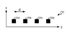
FIG. 2 shows an exemplary design of a
The access point 290 (i.e., another device) may be located within the LOS coverage of the
In general, the
The
The antenna element may be formed on a plane corresponding to the surface of the wireless device and may be used to transmit and / or receive signals. The antenna element may have a particular antenna beam pattern and a particular maximum antenna gain, which may be dependent on the design and implementation of the antenna element. Multiple antenna elements may be formed on the same plane and used to improve antenna gain. The higher antenna gain is more advantageous because (i) it is difficult to efficiently generate high power at the mm-wave frequency, and (ii) the attenuation loss is greater at the mm-wave frequency, , ≪ / RTI > Each antenna element may have a limited LOS coverage area due to the directivity of its antenna element. An antenna system composed of a plurality of antenna elements may also have a limited LOS coverage area. Areas outside the LOS coverage area may be covered by the reflected signals, but the signal strength may be weak in the NLOS coverage area. For this reason, it is desirable to have a larger LOS coverage area if possible.
In an aspect, a wireless device may include a 3-D antenna system to improve LOS coverage and enhance performance. A 3-D antenna system may include antenna elements formed on a plurality of planes pointing to different spatial orientations. Next, the 3-D antenna system may have a plurality of antenna beams corresponding to a plurality of planes where the antenna elements are formed. The antenna beam for each plane may cover different LOS coverage areas. The multiple antenna beams may provide a larger overall LOS coverage area for the wireless device. NLOS coverage can also be improved because antenna beams pointing to different spatial directions can result in reflected signals at higher power levels due to better signal reflection for some antenna beams.
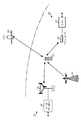
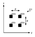
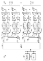
FIG. 3 shows an exemplary design of a
The access point 390 (i.e., another device) is within the LOS coverage of the
As shown in FIGS. 2 and 3, the LOS coverage of
The NLOS coverage of the
Figure 3 shows an exemplary design of a 3-D antenna system including two
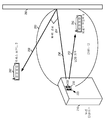
4A illustrates an exemplary design of a
4B shows an exemplary design of a
Figures 4A and 4B show two exemplary designs of a 3-D antenna system. The 3-D antenna system may also be implemented in other ways. For example, a 3-D antenna system may have antenna arrays on the front and two sides (but not the top), or antenna arrays on the front and rear (but not the top or sides) The antenna arrays on the front, rear, and two sides (but not the top), or antenna arrays on the front, rear, top, and two sides. The 3-D antenna system may also include other types of antennas (instead of patch antennas) and / or antennas arranged in different formations (instead of 2-D arrays).
In general, a 3-D antenna system may include any type or combination of antennas of any type. For example, a 3-D antenna system may include a plurality of antenna elements such as patch antennas, monopole antennas, dipole antennas, loop antennas, microstrip antennas, stripline antennas, printed dipole antennas, inverted F antennas, Planar inverted F antennas, polarized patches, plate antennas (which are irregularly shaped planar antennas without any ground plane), half-wave antennas, quarter-wave antennas And the like. The patch antenna is also referred to as a planar antenna. The dipole antenna is also referred to as a whip antenna. The appropriate type of antennas for use in a 3-D antenna system may be selected based on various factors such as the operating frequency of the wireless device, the desired performance, and so on. Some exemplary designs of patch antennas suitable for use at 60 GHz (e.g., for 802.11ad) are described below.
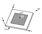
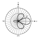
5A shows an exemplary design of a
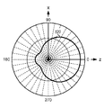
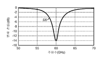
FIG. 5B shows a plot of the
FIG. 5C shows a
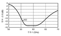
6A shows an exemplary design of a
FIG. 6B shows a plot of the
6C shows a
Figures 5A and 6A illustrate two exemplary patch antenna designs. The patch antenna may also be implemented with other shapes such as rectangular, circular, elliptical, H, O, T, V, W, X, Y, Z, The different shapes may be associated with different bandwidths and / or different antenna beam patterns. A suitable patch shape may be selected based on the desired performance, for example, the desired bandwidth. In general, various aspects of the antenna, such as antenna beam pattern, bandwidth, maximum antenna gain, etc., may depend on various factors such as the shape and dimensions of the antenna, the materials used to implement the antenna,
Multiple patch antennas may be arranged in various formations to form an antenna array. The different array formations may be associated with different antenna beam patterns and different maximum antenna gains.
7A shows an exemplary design of a
FIG. 7B shows a plot of the
FIG. 7C shows a plot of the
8A shows an exemplary design of a
FIG. 8B shows a plot of the
9 shows an exemplary design of an
Figures 7A, 8A, and 9 illustrate several exemplary antenna arrays. In general, multiple patch antennas may be arranged in any formation that can be selected based on various factors such as the desired antenna beam pattern, the desired maximum antenna gain, available space, and the like. The more patch antennas that are lined up in a given axis are the more focused narrow antenna beams, but they can provide higher antenna gain. In addition, a number of patch antennas line up in a given axis may be used for beamforming as described below.
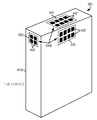
10 shows a side view of an exemplary design of a 3-
Antennas 1022 and 1032 are formed on the
Table 1 lists the different methods of forming antennas in a 3-D antenna system. As shown in Table 1, the antenna elements may be formed on an integrated circuit (IC) chip, on an IC package, on a circuit board, or on a glass substrate (e.g., as shown in FIG. 10). An on-chip implementation can provide for ease of integration, but can be costly due to the high cost per unit area of the IC chip. An on-package implementation may be compact, but may require a customized IC package. An on-board implementation (depending on the material used for the circuit board) can provide good performance and provide flexibility. On-glass implementations can have certain advantages such as lower cost, simple integration with microelectromechanical systems (MEMS) technology, and ease of 3-D fabrication. Based on MEMS or some other process technology, antenna elements may be formed on the glass. The antennas in the 3-D antenna system may be fabricated based on any one of the schemes listed in Table 1 or on any combination of the schemes and / or in other manners. In Table 1, smaller loss tangent is better and loss can be reduced.

In general, a wireless device may include antenna elements (e.g., patch antennas) formed on any number of planes in any size, spherical, or some other shape. In addition, any number of antenna elements may be formed on a given plane. The number of planes to use, the number of antenna elements on each plane, and the design of each antenna element can be flexibly selected based on the requirements of the wireless device.
In an exemplary design, beamforming can be used in a 3-D antenna system to improve LOS coverage and / or achieve other benefits. Beamforming may be performed on one or more antenna arrays in a 3-D antenna system. Beamforming can be used to steer the antenna beam of the antenna array in different spatial directions, which in turn can extend the LOS coverage of the antenna array. Beamforming may be performed on an array of antennas by applying complex gains to a plurality of signals transmitted over different antennas of the array.
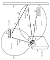
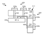
FIG. 11 shows a block diagram of an exemplary design of a
For data transmission,
Within
Each remaining transmission section 1152 similarly receives and processes its data signal using a set of complex gains for its associated antenna array 1130 to produce a set of scaled data signals . The scaled data signals are further processed and may be transmitted via the N antennas 1132 of the associated antenna array 1130.
For data reception,
Within receive
Controller /
All or a portion of the
The
In one exemplary design, the
In another exemplary design,
In general, the
As shown in FIG. 11, a set of complex gains or coefficients may be used for each antenna array 1130 to perform beamforming for that antenna array. The complex gain can be defined by (i) a real value A and an imaginary value B (i.e., A + jB) or (ii) an amplitude K and a phase θ (i.e., K ??). In one exemplary design, the complex gains for each antenna array 1130 may have different amplitudes and / or phases that may be selected to obtain the desired antenna beam. This exemplary design can provide more flexibility to define the antenna beam for the antenna array. In other exemplary designs, the complex gains for each antenna array 1130 have the same amplitude (e.g., 1.0), but may have different phases that can be selected to obtain the desired antenna beam. This exemplary design may allow the total transmit power to be utilized for each antenna 1132. [ In an exemplary design, one complex gain at a set of complex gains for the antenna array may have a fixed value (e.g., 1.0). This may allow one multiplier (e.g.,
Multiple sets of complex gains associated with different antenna beams may be available for the antenna array. In one exemplary design, the plurality of sets of complex gains can be determined (i) a priori by computer simulations, based on empirical measurements, and / or by other means, and (ii) Volatile memory (e.g., memory 1192). For example, M sets of complex gains for M antenna beams pointing to different spatial directions (e.g., evenly spaced from one another in the spatial domain) can be determined and stored, where M can be any integer value have. One set of complex gains can be applied at any given moment to obtain the antenna beam associated with the complex gains of the set.
In another exemplary design, the plurality of sets of complex gains for the antenna array may be adaptively determined. For example, an initial set of complex gains may be used for the antenna array, and a performance metric may be determined for this initial set. One or more complex gains of the initial set may be varied within a predetermined range to obtain a new set of complex gains. The complex gain (s) may be varied at random or based on a search algorithm. A performance metric can be determined for a new set of complex gains. The new set of complex gains can be maintained if the performance metric for the new set is better than the performance metric for the initial set. One or more complex gains may be repeatedly varied and evaluated in a similar manner until a best performance metric is obtained.
In an exemplary design, the device may include first and second sets of antenna elements, for example, as shown in Figs. 3 and 11. Fig. The device may be a wireless device, an antenna module, an IC chip, an IC package, a circuit board, or the like. A first set of antenna elements (e.g.,
In an exemplary design, for example, as shown in Figure 3, the first plane may correspond to the front surface of the wireless device and the second plane may correspond to the top surface of the wireless device. The first and second planes may also correspond to different surfaces of the wireless device.
In an exemplary design, the second set of antenna elements may be associated with a second antenna beam obtained, for example, by beamforming through a second set of complex gains for a second set of antenna elements. In general, beamforming may be performed only for the first set of antenna elements or for both the first and second sets of antenna elements. The beamforming may also be performed independently for the first and second sets of antenna elements, e.g., using different sets of complex gains for the two sets of antenna elements. Alternatively, beamforming may be performed jointly for two sets of antenna elements, for example, using the same set of complex gains for all of the sets of antenna elements.
In an exemplary design, a first set of antenna elements may emit an output signal through a first antenna beam, and a second set of antenna elements may also emit an output signal via a second antenna beam. In this exemplary design, the same output signal can be transmitted from both sets of antenna elements. In another exemplary design, different output signals may be transmitted from the first and second sets of antenna elements.
In an exemplary design, the same antenna beam may be used for both transmission and reception. In this exemplary design, the first set of antenna elements may receive a signal from another device via the first antenna beam. In other exemplary designs, different antenna beams may be used for transmission and reception. In this exemplary design, for example, as shown in FIG. 11, a first set of antenna elements may be coupled to another antenna element, such as, for example, another antenna element obtained by beamforming through a different set of complex gains for the first set of antenna elements The beam can receive signals from other devices.
The apparatus may further comprise first and second sets of power amplifiers, for example, as shown in FIG. A first set of power amplifiers (e.g.,
The apparatus may further comprise first and second sets of LNAs, for example, as shown in FIG. A first set of LNAs (e.g., LNAs 1170 of receive
In an exemplary design, the first set of antenna elements may form a first antenna array, and the second set of antenna elements may form a second antenna array. In an exemplary design, the first set of antenna elements may comprise a plurality of patch antennas that may be arranged in a 2-D array. In the exemplary design, as shown in FIG. 5A, each patch antenna may have a square shape. In another exemplary design, each patch antenna may have a non-square shape, i.e., any shape that is not a rectangle or a square. For example, as shown in FIG. 6A, each patch antenna may have an E shape.
In an exemplary design, a first set of antenna elements may be formed on a first surface of a glass substrate, for example, as shown in Figure 10, and a second set of antenna elements may be formed on a second surface of a glass substrate . The second surface may be perpendicular to the first surface. In other exemplary designs, as listed in Table 1, the first and second sets of antenna elements may be formed on an IC chip, an IC package, a circuit board, or the like.
In an exemplary design, the apparatus may further comprise a memory for storing a plurality of sets of complex gains associated with different antenna beams for a first set of antenna elements. The first set of complex gains for the first set of antenna elements may be one of a plurality of sets of complex gains. In an exemplary design, the first set of complex gains can have the same amplitude and varying phases (i.e., possibly different phases). In another exemplary design, the first set of complex gains may have variable amplitudes and variable phases (i.e., possibly different amplitudes and phases).
In an exemplary design, the first and second sets of antenna elements may operate at a millimeter wave frequency of 40 to 300 GHz. The first and second sets of antenna elements may also operate in different frequency ranges.
The device may also include one or more additional sets of antenna elements formed on one or more additional planes of the wireless device. Each set of antenna elements may be associated with a respective antenna beam pointing to a different spatial orientation. The first, second, and possibly additional sets of antenna elements may provide better LOS coverage and possibly better NLOS coverage for the wireless device.
12 shows an exemplary design of a
In an exemplary design, the first and second signals may comprise the same output signal. This exemplary design can improve the LOS coverage of the wireless device. In another exemplary design, the first and second signals may comprise different output signals. This exemplary design may enable a wireless device to transmit to multiple other devices simultaneously, for example, as shown in FIG.
In an exemplary design, a performance metric for a first set of antenna elements may be determined for each of a plurality of sets of complex gains corresponding to different antenna beams (block 1216). A set of complex gains can be selected from a plurality of sets of complex gains based on a performance metric for each of the plurality of sets of complex gains (block 1218). The complex gains of the selected set may be used for beamforming for the first set of antenna elements.
In an exemplary design, a third signal may be received via the first set of antenna elements. The third signal may be received, for example, by a first set of complex gains for a first set of antenna elements or by beamforming through a third set of complex gains. The fourth signal may be received via a second set of antenna elements. The fourth signal may be received, for example, by a second set of complex gains for a first set of antenna elements or a beamforming through a fourth set of complex gains. For each set of antenna elements, the same antenna beams may be used for both transmission and reception, or different antenna beams may be used for transmission and reception.
Certain portions of a wireless device with the 3-D antenna system described herein may be implemented on an IC, an analog IC, an RFIC, a mixed-signal IC, an ASIC, a printed circuit board (PCB) . Circuits that support the transmission and / or reception of signals through a 3-D antenna system may be implemented using various IC process technologies, such as complementary metal oxide semiconductor (CMOS), N-channel MOS (NMOS) Bipolar junction transistors (BJTs), bipolar junction transistors (BMOS), silicon germanium (SiGe), gallium arsenide (GaAs), heterojunction bipolar transistors (HBTs) Transistors, high electron mobility transistors (HEMTs), silicon-on-insulators (SOI), and the like.
An apparatus with the 3-D antenna system described herein may be a stand-alone device or may be part of a larger device. (I) a set of one or more ICs that may include (i) a standalone IC, (ii) memory ICs for storing data and / or instructions, (iii) an RF receiver (RFR) An RFIC such as a Radio Frequency Identification (RF) receiver (RTR), (iv) an ASIC such as a mobile station modem (MSM), (v) a module that may be embedded in other devices, (vi) a receiver, , (vii), and the like.
In one or more exemplary designs, the functions described may be implemented in hardware, software, firmware, or any combination thereof. When implemented in software, the functions may be stored on or transmitted via one or more instructions or code on a computer-readable medium. Computer-readable media includes both computer storage media and communication media including any medium that facilitates the transfer of computer programs from one place to another. The storage medium may be any available media that can be accessed by a computer. By way of example, and not limitation, such computer-readable media can be RAM, ROM, EEPROM, CD-ROM or other optical disk storage, magnetic disk storage or other magnetic storage devices, Or any other medium that can be used to carry or store the desired program code in the form of data structures. Also, any connection means is appropriately named as a computer-readable medium. For example, if software is transmitted from a website, server, or other remote source using wireless technologies such as coaxial cable, fiber optic cable, twisted pair, digital subscriber line (DSL), or infrared, radio and microwave, , Fiber optic cable, twisted pair, DSL, or wireless technologies such as infrared, radio and microwave are included within the definition of medium. As used herein, a disk and a disc may be referred to as a compact disc (CD), a laser disc, an optical disc, a digital versatile disc (DVD) A floppy disk and a blu-ray disc wherein the disks typically reproduce the data magnetically while the discs drive the data through the lasers optically . Combinations of the foregoing should also be included within the scope of computer-readable media.
The previous description of the disclosure is provided to enable any person skilled in the art to make or use the disclosure. Various modifications to the disclosure will be readily apparent to those skilled in the art, and the generic principles defined herein may be applied to other variations without departing from the scope of the disclosure. Accordingly, this disclosure is not intended to be limited to the examples and designs described herein, but is to be accorded the widest scope consistent with the principles and novel features disclosed herein.
Claims (20)
A first set of antenna elements formed on a first plane of the wireless device and associated with a first antenna beam obtained by beamforming; And
A second set of antenna elements formed on a second plane of the wireless device,
The first plane and the second plane pointing to different spatial orientations,
Device.
Wherein the beamforming is through a first set of complex gains for the first set of antenna elements,
Device.
The second set of antenna elements being associated with a second antenna beam obtained by beamforming through a second set of complex gains for the second set of antenna elements,
Device.
The first set of antenna elements radiating an output signal through the first antenna beam,
The second set of antenna elements emitting the output signal through a second antenna beam,
Device.
The first set of antenna elements receiving a signal from another device via the first antenna beam,
Device.
Configured to receive a first set of input signals generated based on a first output signal and to provide a first set of output radio frequency (RF) signals for transmission over the first set of antenna elements A first set of power amplifiers; And
Configured to receive a second set of input signals generated based on the first output signal or a second output signal and to provide a second set of output RF signals for transmission on the second set of antenna elements Further comprising two sets of power amplifiers,
Device.
A first set of low noise amplifiers (LNAs) configured to receive a first set of received radio frequency (RF) signals from the first set of antenna elements and to provide a first set of amplified signals, amplifiers); And
Further comprising a second set of LNAs configured to receive a second set of received RF signals from the second set of antenna elements and to provide a second set of amplified signals,
Device.
Wherein the first plane is perpendicular to the second plane,
Device.
The first set of antenna elements including a plurality of patch antennas,
Device.
Each of the plurality of patch antennas having a non-square shape or an E-
Device.
The first set of antenna elements being formed on a first surface of a glass substrate,
The second set of antenna elements being formed on a second surface of the glass substrate,
Device.
Further comprising a memory configured to store a plurality of sets of complex gains associated with different antenna beams for the first set of antenna elements,
Wherein the first set of complex gains is one of the plurality of sets of complex gains,
Device.
The complex gains in the first set having the same amplitude and varying phases,
Device.
Wherein the first set of antenna elements and the second set of antenna elements operate at a millimeter wave frequency of 40 to 300 gigahertz (GHz)
Device.
Transmitting a first signal by beamforming from a first set of antenna elements formed on a first plane of the wireless device; And
And transmitting a second signal from a second set of antenna elements formed on a second plane of the wireless device,
The first plane and the second plane pointing to different spatial orientations,
Way.
The first signal being transmitted by beamforming through a first set of complex gains for the first set of antenna elements,
The second signal being transmitted by beamforming through a second set of complex gains for the second set of antenna elements,
Way.
Determining a performance metric for the first set of antenna elements for each of a plurality of sets of complex gains corresponding to different antenna beams; And
Further comprising selecting a set of complex gains from the plurality of sets of complex gains based on the performance metric for each of the plurality of sets of complex gains,
Wherein the first signal is transmitted by beamforming through a selected set of complex gains,
Way.
Further comprising receiving a third signal by beamforming through the first set of antenna elements,
Way.
Means for transmitting a first signal by beamforming from a first set of antenna elements formed on a first plane of the wireless device; And
And means for transmitting a second signal from a second set of antenna elements formed on a second plane of the wireless device,
The first plane and the second plane pointing to different spatial orientations,
Device.
Means for determining a performance metric for the first set of antenna elements for each of a plurality of sets of complex gains corresponding to different antenna beams; And
Means for selecting a set of complex gains from the plurality of sets of complex gains based on the performance metric for each of the plurality of sets of complex gains,
Wherein the first signal is transmitted by beamforming through a selected set of complex gains,
Device.
Applications Claiming Priority (3)
| Application Number | Priority Date | Filing Date | Title |
|---|---|---|---|
| US13/223,127 US9905922B2 (en) | 2011-08-31 | 2011-08-31 | Wireless device with 3-D antenna system |
| US13/223,127 | 2011-08-31 | ||
| PCT/US2012/053545 WO2013033650A1 (en) | 2011-08-31 | 2012-08-31 | Wireless device with 3-d antenna system |
Related Child Applications (1)
| Application Number | Title | Priority Date | Filing Date |
|---|---|---|---|
| KR1020167022734A Division KR101874077B1 (en) | 2011-08-31 | 2012-08-31 | Wireless device with 3-d antenna system |
Publications (1)
| Publication Number | Publication Date |
|---|---|
| KR20140053396A true KR20140053396A (en) | 2014-05-07 |
Family
ID=46846021
Family Applications (2)
| Application Number | Title | Priority Date | Filing Date |
|---|---|---|---|
| KR1020147008379A KR20140053396A (en) | 2011-08-31 | 2012-08-31 | Wireless device with 3-d antenna system |
| KR1020167022734A KR101874077B1 (en) | 2011-08-31 | 2012-08-31 | Wireless device with 3-d antenna system |
Family Applications After (1)
| Application Number | Title | Priority Date | Filing Date |
|---|---|---|---|
| KR1020167022734A KR101874077B1 (en) | 2011-08-31 | 2012-08-31 | Wireless device with 3-d antenna system |
Country Status (7)
| Country | Link |
|---|---|
| US (1) | US9905922B2 (en) |
| EP (1) | EP2751869A1 (en) |
| JP (1) | JP5925894B2 (en) |
| KR (2) | KR20140053396A (en) |
| CN (1) | CN103765674B (en) |
| IN (1) | IN2014CN00435A (en) |
| WO (1) | WO2013033650A1 (en) |
Cited By (1)
| Publication number | Priority date | Publication date | Assignee | Title |
|---|---|---|---|---|
| KR20200025439A (en) * | 2018-08-30 | 2020-03-10 | 삼성전자주식회사 | Electronic device comprising 5g antenna module |
Families Citing this family (66)
| Publication number | Priority date | Publication date | Assignee | Title |
|---|---|---|---|---|
| EP2551695A1 (en) * | 2011-07-25 | 2013-01-30 | Fraunhofer-Gesellschaft zur Förderung der angewandten Forschung e.V. | Concept for determining an orientation of a mobile device |
| EP2956989B1 (en) * | 2013-02-06 | 2017-10-04 | Telefonaktiebolaget LM Ericsson (publ) | Antenna arrangement for multiple frequency band operation |
| GB2517770A (en) * | 2013-09-02 | 2015-03-04 | Nokia Technologies Oy | Apparatus and methods for wireless communication |
| KR102056411B1 (en) | 2014-02-28 | 2019-12-16 | 삼성전자주식회사 | Method and apparatus for beam coverage expansion in wireless communication system |
| US9799954B2 (en) * | 2014-08-29 | 2017-10-24 | Advanced Micro Devices, Inc. | Apparatus with multi-directional radiation capability using multiple antenna elements |
| US10615499B2 (en) | 2015-01-14 | 2020-04-07 | Skywave Mobile Communications Inc. | Dual role antenna assembly |
| US20160218426A1 (en) * | 2015-01-26 | 2016-07-28 | Nitero Pty Ltd. | Power management in wireless communications devices |
| US9653818B2 (en) | 2015-02-23 | 2017-05-16 | Qualcomm Incorporated | Antenna structures and configurations for millimeter wavelength wireless communications |
| CN104752832B (en) * | 2015-03-02 | 2018-08-10 | 联想(北京)有限公司 | A kind of Alignment Method and electronic equipment |
| JP6701724B2 (en) * | 2015-12-25 | 2020-05-27 | セイコーエプソン株式会社 | Display device, projector, and communication device |
| JP6872652B6 (en) * | 2016-02-12 | 2021-06-23 | パナソニック インテレクチュアル プロパティ コーポレーション オブ アメリカPanasonic Intellectual Property Corporation of America | Display method in wireless communication device and wireless communication device |
| JP6847581B2 (en) | 2016-02-12 | 2021-03-24 | パナソニック インテレクチュアル プロパティ コーポレーション オブ アメリカPanasonic Intellectual Property Corporation of America | Display method in wireless communication device and wireless communication device |
| JP6818757B2 (en) * | 2016-04-01 | 2021-01-20 | アップル インコーポレイテッドApple Inc. | Beamforming architecture for multi-beam multi-input multi-output (MIMO) |
| US9912061B2 (en) * | 2016-05-18 | 2018-03-06 | International Business Machines Corporation | Millimeter-wave communications on a multifunction platform |
| KR101852580B1 (en) * | 2016-08-31 | 2018-06-11 | 엘지전자 주식회사 | Antenna system loaded in vehicle |
| US10651551B2 (en) * | 2016-12-06 | 2020-05-12 | Commscope Technologies Llc | Antenna radome-enclosures and related antenna structures |
| USD873249S1 (en) | 2016-12-06 | 2020-01-21 | Commscope Technologies Llc | Antenna radome enclosure and a radome |
| EP3340378A1 (en) * | 2016-12-22 | 2018-06-27 | Centre National d'Etudes Spatiales | A simplified gnss receiver with improved precision in a perturbated environment |
| JP6572924B2 (en) * | 2017-03-02 | 2019-09-11 | Tdk株式会社 | Antenna device |
| EP3598579A4 (en) * | 2017-03-15 | 2020-03-04 | Sony Mobile Communications Inc. | Communication device |
| JP2019140658A (en) * | 2017-03-21 | 2019-08-22 | 京セラ株式会社 | Composite antenna, radio communication module, and radio communication equipment |
| CN110870136B (en) | 2017-03-24 | 2021-08-31 | 伊索电子股份有限公司 | Zero-steering antenna technique for advanced communication systems |
| JP6750738B2 (en) * | 2017-06-14 | 2020-09-02 | 株式会社村田製作所 | Antenna module and communication device |
| CN107317121A (en) * | 2017-06-29 | 2017-11-03 | 昆山睿翔讯通通信技术有限公司 | A kind of mobile terminal based on three-dimensional millimeter wave array antenna |
| US10665959B2 (en) | 2017-07-24 | 2020-05-26 | Apple Inc. | Millimeter wave antennas having dual patch resonating elements |
| EP3683891B1 (en) * | 2017-10-19 | 2024-04-10 | Sony Group Corporation | Antenna device |
| JP6606158B2 (en) * | 2017-11-20 | 2019-11-13 | アンリツ株式会社 | Wireless terminal measuring apparatus and wireless terminal measuring method |
| KR102426656B1 (en) * | 2017-11-28 | 2022-07-28 | 삼성전자주식회사 | The electronic device comprising an antenna |
| CN108232470A (en) * | 2017-12-13 | 2018-06-29 | 瑞声科技(南京)有限公司 | A kind of antenna system and mobile terminal |
| CN111433976A (en) * | 2017-12-14 | 2020-07-17 | 株式会社村田制作所 | Antenna device, antenna module, and wireless device |
| CN107946780A (en) * | 2017-12-18 | 2018-04-20 | 罗森伯格技术(昆山)有限公司 | A kind of integrated antenna for base station |
| WO2019146183A1 (en) * | 2018-01-26 | 2019-08-01 | ソニー株式会社 | Antenna device |
| CN108322229B (en) * | 2018-01-31 | 2021-06-22 | 深圳市盛路物联通讯技术有限公司 | Radio frequency receiving circuit, circuit board, chip and terminal of Internet of things |
| CN108418594B (en) * | 2018-01-31 | 2021-06-22 | 深圳市盛路物联通讯技术有限公司 | Multipurpose high signal-to-noise ratio type Internet of things radio frequency circuit, circuit board, chip and terminal |
| KR102472237B1 (en) | 2018-03-09 | 2022-11-30 | 삼성전자주식회사 | Electronic device for including antenna |
| CN108718203B (en) * | 2018-03-30 | 2021-06-22 | 深圳市盛路物联通讯技术有限公司 | Anti-interference type thing networking radio frequency circuit and terminal |
| CN108429558B (en) * | 2018-03-30 | 2021-06-22 | 深圳市盛路物联通讯技术有限公司 | Double-balanced mixing type radio frequency circuit based on PIFA antenna and terminal |
| CN108599800A (en) * | 2018-03-30 | 2018-09-28 | 深圳市盛路物联通讯技术有限公司 | Internet of Things radio circuit and terminal based on PIFA antennas and lumped parameter matching type |
| KR102468136B1 (en) | 2018-04-23 | 2022-11-18 | 삼성전자 주식회사 | Antenna device and electronic device comprising the same |
| KR102482148B1 (en) | 2018-05-16 | 2022-12-29 | 삼성전자주식회사 | Electronic device comprising antenna and method thereof |
| US20200021010A1 (en) * | 2018-07-13 | 2020-01-16 | Qualcomm Incorporated | Air coupled superstrate antenna on device housing |
| KR20200014601A (en) | 2018-08-01 | 2020-02-11 | 삼성전자주식회사 | Electronic device for including antenna array |
| WO2020031776A1 (en) * | 2018-08-06 | 2020-02-13 | 株式会社村田製作所 | Antenna module |
| EP3832798B1 (en) * | 2018-08-17 | 2023-10-11 | Huawei Technologies Co., Ltd. | Antenna assembly and antenna tuning-free method and device |
| KR20200024408A (en) * | 2018-08-28 | 2020-03-09 | 삼성전자주식회사 | Electronic device for including antenna array |
| JP2020065246A (en) * | 2018-10-16 | 2020-04-23 | 株式会社村田製作所 | Communication device |
| KR102341998B1 (en) * | 2018-10-30 | 2021-12-22 | 엘지전자 주식회사 | Antenna system mounted on a vehicle and a vehicle having the same |
| KR102562631B1 (en) | 2018-11-26 | 2023-08-02 | 삼성전자 주식회사 | Antenna and electronic device including the same |
| US11362421B2 (en) * | 2018-12-27 | 2022-06-14 | Qualcomm Incorporated | Antenna and device configurations |
| DE212019000431U1 (en) * | 2018-12-28 | 2021-07-05 | Murata Manufacturing Co., Ltd. | Communication device |
| KR20200084617A (en) * | 2019-01-03 | 2020-07-13 | 삼성전자주식회사 | Antenna using conductive side member and electronic device including the same |
| EP3891841B1 (en) | 2019-01-03 | 2024-03-06 | Huawei Technologies Co., Ltd. | Beam steering antenna structure and electronic device comprising said structure |
| US11171408B2 (en) * | 2019-05-23 | 2021-11-09 | Htc Corporation | Communication device |
| EP3772826B1 (en) * | 2019-08-05 | 2021-12-01 | Samsung Electronics Co., Ltd. | Antenna module and electronic device for using the antenna module |
| WO2021040892A1 (en) * | 2019-08-30 | 2021-03-04 | Commscope Technologies Llc | Base station antennas having low cost wideband cross-dipole radiating elements |
| KR20210056609A (en) | 2019-11-11 | 2021-05-20 | 부산대학교 산학협력단 | Simulation technique for GNSS-RO data based on wave optics |
| KR20210063763A (en) | 2019-11-25 | 2021-06-02 | 삼성전자주식회사 | Electronic device including antenna |
| US11404765B2 (en) | 2020-06-26 | 2022-08-02 | GlaiveRF, Inc. | Retractable phased array for mobile devices |
| US11303012B2 (en) | 2020-08-14 | 2022-04-12 | GlaiveRF, Inc. | Mobile device case with phased array antenna system |
| CN112448131B (en) * | 2020-11-12 | 2022-12-13 | 厦门亿联网络技术股份有限公司 | Antenna structure and radio base station |
| CN115642394A (en) * | 2021-07-19 | 2023-01-24 | Oppo广东移动通信有限公司 | Antenna module and communication equipment |
| CN113644400B (en) * | 2021-07-23 | 2024-04-12 | 荣耀终端有限公司 | Millimeter wave module circuit and terminal equipment |
| US11784418B2 (en) * | 2021-10-12 | 2023-10-10 | Qualcomm Incorporated | Multi-directional dual-polarized antenna system |
| WO2023157390A1 (en) * | 2022-02-16 | 2023-08-24 | 株式会社村田製作所 | Antenna module and communication device equipped with same |
| WO2023187895A1 (en) * | 2022-03-28 | 2023-10-05 | 日本電気株式会社 | Control device, terminal device, control method, and non-transitory computer-readable medium |
| US20240022281A1 (en) * | 2022-07-13 | 2024-01-18 | Qualcomm Incorporated | Antenna side combining or antenna side selection in an l-shaped antenna module |
Family Cites Families (20)
| Publication number | Priority date | Publication date | Assignee | Title |
|---|---|---|---|---|
| DE4321430A1 (en) * | 1993-06-28 | 1995-01-05 | Henkel Kgaa | Dishwashing detergent with biodegradable builder component II |
| EP0763264A1 (en) * | 1994-06-03 | 1997-03-19 | Telefonaktiebolaget Lm Ericsson | Microstrip antenna array |
| JP4435371B2 (en) | 2000-04-17 | 2010-03-17 | 国立大学法人横浜国立大学 | Directivity control wireless communication device |
| US6426726B1 (en) * | 2001-08-15 | 2002-07-30 | Northrop Grumman Corporation | Polarized phased array antenna |
| JP2005539458A (en) | 2002-09-17 | 2005-12-22 | アイピーアール ライセンシング インコーポレイテッド | Multi-pattern antenna |
| JP2005045598A (en) | 2003-07-23 | 2005-02-17 | Sony Corp | Portable information terminal device |
| US20060038738A1 (en) * | 2004-08-18 | 2006-02-23 | Video54 Technologies, Inc. | Wireless system having multiple antennas and multiple radios |
| US20060038739A1 (en) | 2004-08-21 | 2006-02-23 | I-Peng Feng | Spiral cylindrical ceramic circular polarized antenna |
| US7358912B1 (en) * | 2005-06-24 | 2008-04-15 | Ruckus Wireless, Inc. | Coverage antenna apparatus with selectable horizontal and vertical polarization elements |
| US20060276157A1 (en) | 2005-06-03 | 2006-12-07 | Chen Zhi N | Apparatus and methods for packaging antennas with integrated circuit chips for millimeter wave applications |
| US20070097009A1 (en) * | 2005-11-01 | 2007-05-03 | Torres Alfonso R | Planar slot antenna design using optically transmissive materials |
| US7884776B2 (en) | 2006-09-28 | 2011-02-08 | Farrokh Mohamadi | High power integrated circuit beamforming array |
| US7768457B2 (en) * | 2007-06-22 | 2010-08-03 | Vubiq, Inc. | Integrated antenna and chip package and method of manufacturing thereof |
| EP2068400A1 (en) | 2007-12-03 | 2009-06-10 | Sony Corporation | Slot antenna for mm-wave signals |
| DE102007061738A1 (en) * | 2007-12-20 | 2009-06-25 | Robert Bosch Gmbh | Antenna, in particular for radar signals, and method and use |
| EP2117078B1 (en) * | 2008-05-05 | 2017-07-05 | Nokia Solutions and Networks Oy | Patch antenna element array |
| JP5248233B2 (en) * | 2008-08-04 | 2013-07-31 | 日本信号株式会社 | Display panel and reader / writer system |
| IL194364A0 (en) * | 2008-09-25 | 2009-08-03 | Zeev Roth | A method and system for allocating wireless transmission resources |
| US8013784B2 (en) * | 2009-03-03 | 2011-09-06 | Toyota Motor Engineering & Manufacturing North America, Inc. | Butler matrix for 3D integrated RF front-ends |
| US20140225805A1 (en) | 2011-03-15 | 2014-08-14 | Helen K. Pan | Conformal phased array antenna with integrated transceiver |
-
2011
- 2011-08-31 US US13/223,127 patent/US9905922B2/en active Active
-
2012
- 2012-08-31 EP EP12758960.4A patent/EP2751869A1/en not_active Withdrawn
- 2012-08-31 CN CN201280042420.5A patent/CN103765674B/en active Active
- 2012-08-31 KR KR1020147008379A patent/KR20140053396A/en active Application Filing
- 2012-08-31 IN IN435CHN2014 patent/IN2014CN00435A/en unknown
- 2012-08-31 JP JP2014528677A patent/JP5925894B2/en active Active
- 2012-08-31 KR KR1020167022734A patent/KR101874077B1/en active IP Right Grant
- 2012-08-31 WO PCT/US2012/053545 patent/WO2013033650A1/en unknown
Cited By (2)
| Publication number | Priority date | Publication date | Assignee | Title |
|---|---|---|---|---|
| KR20200025439A (en) * | 2018-08-30 | 2020-03-10 | 삼성전자주식회사 | Electronic device comprising 5g antenna module |
| US11901610B2 (en) | 2018-08-30 | 2024-02-13 | Samsung Electronics Co., Ltd. | Electronic apparatus including antenna module |
Also Published As
| Publication number | Publication date |
|---|---|
| KR20160103158A (en) | 2016-08-31 |
| WO2013033650A1 (en) | 2013-03-07 |
| CN103765674A (en) | 2014-04-30 |
| JP5925894B2 (en) | 2016-05-25 |
| JP2014529971A (en) | 2014-11-13 |
| CN103765674B (en) | 2016-10-05 |
| IN2014CN00435A (en) | 2015-04-03 |
| EP2751869A1 (en) | 2014-07-09 |
| KR101874077B1 (en) | 2018-07-03 |
| US20130050056A1 (en) | 2013-02-28 |
| US9905922B2 (en) | 2018-02-27 |
Similar Documents
| Publication | Publication Date | Title |
|---|---|---|
| KR101874077B1 (en) | Wireless device with 3-d antenna system | |
| US11605904B2 (en) | Phased array antenna module and communication device including the same | |
| US9319155B2 (en) | Multiple input multiple output antenna module and associated method | |
| US9496617B2 (en) | Surface wave launched dielectric resonator antenna | |
| US20200021010A1 (en) | Air coupled superstrate antenna on device housing | |
| CN112753134B (en) | Antenna with gradient index metamaterial | |
| US11362421B2 (en) | Antenna and device configurations | |
| US20130016024A1 (en) | Wideband antenna system with multiple antennas and at least one parasitic element | |
| US11165136B2 (en) | Flex integrated antenna array | |
| US20070069962A1 (en) | Antenna system for a radiocommunication station, and radiocommunication station having such antenna system | |
| KR20170086532A (en) | Cavity backed aperture antenna | |
| WO2012008946A1 (en) | Multiple input - multiple output antenna module | |
| US20140170992A1 (en) | Diversity Antenna Module and Associated Method for a User Equipment (UE) Device | |
| EP2408062A1 (en) | Multiple input - multiple output antenna module | |
| US20180090853A1 (en) | Transmit Device and Method Thereof | |
| US7750855B2 (en) | Compact polarization-sensitive and phase-sensitive antenna with directionality and multi-frequency resonances | |
| US11108168B2 (en) | Antenna system for portable communication device for millimeter wave communication | |
| KR102502237B1 (en) | Phased array antenna module and communication device including the same | |
| US11594823B2 (en) | Discrete antenna module with via wall structure | |
| Elsakka et al. | On the use of focal-plane arrays in mm-wave 5G base stations | |
| Sadhu et al. | Phased arrays for 5G millimeter-wave communications | |
| Li et al. | A planar active antenna array for hybrid phased array-MIMO system | |
| US20220094075A1 (en) | Dual-feed dual-band interleaved antenna configuration | |
| Zhao et al. | Antenna system design and integration for 5G mmWave handset |
Legal Events
| Date | Code | Title | Description |
|---|---|---|---|
| A201 | Request for examination | ||
| E902 | Notification of reason for refusal | ||
| AMND | Amendment | ||
| E601 | Decision to refuse application | ||
| AMND | Amendment | ||
| A107 | Divisional application of patent |