KR20140051232A - Multi-chamber cvd processing system - Google Patents
Multi-chamber cvd processing system Download PDFInfo
- Publication number
- KR20140051232A KR20140051232A KR1020147000821A KR20147000821A KR20140051232A KR 20140051232 A KR20140051232 A KR 20140051232A KR 1020147000821 A KR1020147000821 A KR 1020147000821A KR 20147000821 A KR20147000821 A KR 20147000821A KR 20140051232 A KR20140051232 A KR 20140051232A
- Authority
- KR
- South Korea
- Prior art keywords
- substrate
- chamber
- substrate carrier
- enclosures
- deposition
- Prior art date
Links
- 238000012545 processing Methods 0.000 title claims abstract description 67
- 239000000758 substrate Substances 0.000 claims abstract description 390
- 238000000034 method Methods 0.000 claims abstract description 171
- 238000000151 deposition Methods 0.000 claims abstract description 152
- 230000008021 deposition Effects 0.000 claims abstract description 152
- 238000005229 chemical vapour deposition Methods 0.000 claims abstract description 122
- 230000008569 process Effects 0.000 claims abstract description 119
- 239000000969 carrier Substances 0.000 claims abstract description 118
- 230000032258 transport Effects 0.000 claims abstract description 55
- 230000007723 transport mechanism Effects 0.000 claims abstract description 48
- 238000006243 chemical reaction Methods 0.000 claims abstract description 32
- 238000007789 sealing Methods 0.000 claims abstract description 17
- 239000002243 precursor Substances 0.000 claims description 42
- 238000009826 distribution Methods 0.000 claims description 21
- 238000012625 in-situ measurement Methods 0.000 claims description 10
- 238000010438 heat treatment Methods 0.000 claims description 4
- 238000005424 photoluminescence Methods 0.000 claims description 4
- 238000005452 bending Methods 0.000 claims description 3
- 238000005401 electroluminescence Methods 0.000 claims description 2
- 230000007246 mechanism Effects 0.000 claims 2
- 241000269627 Amphiuma means Species 0.000 claims 1
- 238000004020 luminiscence type Methods 0.000 claims 1
- 239000007789 gas Substances 0.000 description 179
- 235000012431 wafers Nutrition 0.000 description 17
- 239000000463 material Substances 0.000 description 16
- 239000004065 semiconductor Substances 0.000 description 14
- 239000012159 carrier gas Substances 0.000 description 9
- 229910052751 metal Inorganic materials 0.000 description 8
- 239000002184 metal Substances 0.000 description 8
- 239000011261 inert gas Substances 0.000 description 7
- 238000010926 purge Methods 0.000 description 7
- 238000000429 assembly Methods 0.000 description 6
- 230000000712 assembly Effects 0.000 description 6
- 150000001875 compounds Chemical class 0.000 description 6
- 238000011065 in-situ storage Methods 0.000 description 6
- QGZKDVFQNNGYKY-UHFFFAOYSA-N Ammonia Chemical compound N QGZKDVFQNNGYKY-UHFFFAOYSA-N 0.000 description 5
- 239000000203 mixture Substances 0.000 description 5
- 239000006227 byproduct Substances 0.000 description 4
- 238000004140 cleaning Methods 0.000 description 4
- 150000004678 hydrides Chemical class 0.000 description 4
- 238000012986 modification Methods 0.000 description 4
- 230000004048 modification Effects 0.000 description 4
- -1 GaCl 2 Chemical compound 0.000 description 3
- 229910001218 Gallium arsenide Inorganic materials 0.000 description 3
- 229910000577 Silicon-germanium Inorganic materials 0.000 description 3
- 238000011109 contamination Methods 0.000 description 3
- 229910021478 group 5 element Inorganic materials 0.000 description 3
- 150000002739 metals Chemical class 0.000 description 3
- 229910003465 moissanite Inorganic materials 0.000 description 3
- 229910010271 silicon carbide Inorganic materials 0.000 description 3
- 229910002704 AlGaN Inorganic materials 0.000 description 2
- XKRFYHLGVUSROY-UHFFFAOYSA-N Argon Chemical compound [Ar] XKRFYHLGVUSROY-UHFFFAOYSA-N 0.000 description 2
- IJGRMHOSHXDMSA-UHFFFAOYSA-N Atomic nitrogen Chemical compound N#N IJGRMHOSHXDMSA-UHFFFAOYSA-N 0.000 description 2
- VEXZGXHMUGYJMC-UHFFFAOYSA-M Chloride anion Chemical compound [Cl-] VEXZGXHMUGYJMC-UHFFFAOYSA-M 0.000 description 2
- VEXZGXHMUGYJMC-UHFFFAOYSA-N Hydrochloric acid Chemical compound Cl VEXZGXHMUGYJMC-UHFFFAOYSA-N 0.000 description 2
- 229910000661 Mercury cadmium telluride Inorganic materials 0.000 description 2
- 229910007709 ZnTe Inorganic materials 0.000 description 2
- 230000003213 activating effect Effects 0.000 description 2
- 229910021529 ammonia Inorganic materials 0.000 description 2
- 238000000137 annealing Methods 0.000 description 2
- 230000004888 barrier function Effects 0.000 description 2
- 238000009529 body temperature measurement Methods 0.000 description 2
- 239000013626 chemical specie Substances 0.000 description 2
- XOYLJNJLGBYDTH-UHFFFAOYSA-M chlorogallium Chemical compound [Ga]Cl XOYLJNJLGBYDTH-UHFFFAOYSA-M 0.000 description 2
- 238000013461 design Methods 0.000 description 2
- 230000000694 effects Effects 0.000 description 2
- 239000012530 fluid Substances 0.000 description 2
- 150000004820 halides Chemical class 0.000 description 2
- 238000004519 manufacturing process Methods 0.000 description 2
- 230000003446 memory effect Effects 0.000 description 2
- 229910001510 metal chloride Inorganic materials 0.000 description 2
- 230000003071 parasitic effect Effects 0.000 description 2
- 230000002093 peripheral effect Effects 0.000 description 2
- 239000012071 phase Substances 0.000 description 2
- 239000010453 quartz Substances 0.000 description 2
- 238000011160 research Methods 0.000 description 2
- SBIBMFFZSBJNJF-UHFFFAOYSA-N selenium;zinc Chemical compound [Se]=[Zn] SBIBMFFZSBJNJF-UHFFFAOYSA-N 0.000 description 2
- VYPSYNLAJGMNEJ-UHFFFAOYSA-N silicon dioxide Inorganic materials O=[Si]=O VYPSYNLAJGMNEJ-UHFFFAOYSA-N 0.000 description 2
- 239000000126 substance Substances 0.000 description 2
- 238000012546 transfer Methods 0.000 description 2
- 238000011144 upstream manufacturing Methods 0.000 description 2
- 238000000927 vapour-phase epitaxy Methods 0.000 description 2
- XLOMVQKBTHCTTD-UHFFFAOYSA-N zinc oxide Inorganic materials [Zn]=O XLOMVQKBTHCTTD-UHFFFAOYSA-N 0.000 description 2
- 229910000962 AlSiC Inorganic materials 0.000 description 1
- OKTJSMMVPCPJKN-UHFFFAOYSA-N Carbon Chemical compound [C] OKTJSMMVPCPJKN-UHFFFAOYSA-N 0.000 description 1
- GYHNNYVSQQEPJS-UHFFFAOYSA-N Gallium Chemical compound [Ga] GYHNNYVSQQEPJS-UHFFFAOYSA-N 0.000 description 1
- 229910000673 Indium arsenide Inorganic materials 0.000 description 1
- 229910052782 aluminium Inorganic materials 0.000 description 1
- XAGFODPZIPBFFR-UHFFFAOYSA-N aluminium Chemical compound [Al] XAGFODPZIPBFFR-UHFFFAOYSA-N 0.000 description 1
- 229910052787 antimony Inorganic materials 0.000 description 1
- WATWJIUSRGPENY-UHFFFAOYSA-N antimony atom Chemical compound [Sb] WATWJIUSRGPENY-UHFFFAOYSA-N 0.000 description 1
- 238000013459 approach Methods 0.000 description 1
- 229910052786 argon Inorganic materials 0.000 description 1
- RBFQJDQYXXHULB-UHFFFAOYSA-N arsane Chemical compound [AsH3] RBFQJDQYXXHULB-UHFFFAOYSA-N 0.000 description 1
- 238000003877 atomic layer epitaxy Methods 0.000 description 1
- 230000015572 biosynthetic process Effects 0.000 description 1
- 229910052797 bismuth Inorganic materials 0.000 description 1
- JCXGWMGPZLAOME-UHFFFAOYSA-N bismuth atom Chemical compound [Bi] JCXGWMGPZLAOME-UHFFFAOYSA-N 0.000 description 1
- 230000015556 catabolic process Effects 0.000 description 1
- 238000012512 characterization method Methods 0.000 description 1
- 238000004891 communication Methods 0.000 description 1
- 238000001816 cooling Methods 0.000 description 1
- 239000000498 cooling water Substances 0.000 description 1
- 238000006731 degradation reaction Methods 0.000 description 1
- 230000001419 dependent effect Effects 0.000 description 1
- 230000006870 function Effects 0.000 description 1
- 229910052733 gallium Inorganic materials 0.000 description 1
- 239000011521 glass Substances 0.000 description 1
- 229910002804 graphite Inorganic materials 0.000 description 1
- 239000010439 graphite Substances 0.000 description 1
- 231100001261 hazardous Toxicity 0.000 description 1
- 239000001307 helium Substances 0.000 description 1
- 229910052734 helium Inorganic materials 0.000 description 1
- SWQJXJOGLNCZEY-UHFFFAOYSA-N helium atom Chemical compound [He] SWQJXJOGLNCZEY-UHFFFAOYSA-N 0.000 description 1
- 238000004050 hot filament vapor deposition Methods 0.000 description 1
- 239000001257 hydrogen Substances 0.000 description 1
- 229910052739 hydrogen Inorganic materials 0.000 description 1
- 125000004435 hydrogen atom Chemical class [H]* 0.000 description 1
- 229910052738 indium Inorganic materials 0.000 description 1
- RPQDHPTXJYYUPQ-UHFFFAOYSA-N indium arsenide Chemical compound [In]#[As] RPQDHPTXJYYUPQ-UHFFFAOYSA-N 0.000 description 1
- APFVFJFRJDLVQX-UHFFFAOYSA-N indium atom Chemical compound [In] APFVFJFRJDLVQX-UHFFFAOYSA-N 0.000 description 1
- 230000006698 induction Effects 0.000 description 1
- 238000002347 injection Methods 0.000 description 1
- 239000007924 injection Substances 0.000 description 1
- 238000005259 measurement Methods 0.000 description 1
- 238000002156 mixing Methods 0.000 description 1
- 150000004767 nitrides Chemical class 0.000 description 1
- 229910052757 nitrogen Inorganic materials 0.000 description 1
- 230000006911 nucleation Effects 0.000 description 1
- 238000010899 nucleation Methods 0.000 description 1
- 150000002902 organometallic compounds Chemical class 0.000 description 1
- 238000012805 post-processing Methods 0.000 description 1
- 239000012495 reaction gas Substances 0.000 description 1
- 238000002310 reflectometry Methods 0.000 description 1
- 229910052594 sapphire Inorganic materials 0.000 description 1
- 239000010980 sapphire Substances 0.000 description 1
- 229910001220 stainless steel Inorganic materials 0.000 description 1
- 239000010935 stainless steel Substances 0.000 description 1
- 238000012360 testing method Methods 0.000 description 1
Images


Classifications
-
- C—CHEMISTRY; METALLURGY
- C23—COATING METALLIC MATERIAL; COATING MATERIAL WITH METALLIC MATERIAL; CHEMICAL SURFACE TREATMENT; DIFFUSION TREATMENT OF METALLIC MATERIAL; COATING BY VACUUM EVAPORATION, BY SPUTTERING, BY ION IMPLANTATION OR BY CHEMICAL VAPOUR DEPOSITION, IN GENERAL; INHIBITING CORROSION OF METALLIC MATERIAL OR INCRUSTATION IN GENERAL
- C23C—COATING METALLIC MATERIAL; COATING MATERIAL WITH METALLIC MATERIAL; SURFACE TREATMENT OF METALLIC MATERIAL BY DIFFUSION INTO THE SURFACE, BY CHEMICAL CONVERSION OR SUBSTITUTION; COATING BY VACUUM EVAPORATION, BY SPUTTERING, BY ION IMPLANTATION OR BY CHEMICAL VAPOUR DEPOSITION, IN GENERAL
- C23C16/00—Chemical coating by decomposition of gaseous compounds, without leaving reaction products of surface material in the coating, i.e. chemical vapour deposition [CVD] processes
- C23C16/44—Chemical coating by decomposition of gaseous compounds, without leaving reaction products of surface material in the coating, i.e. chemical vapour deposition [CVD] processes characterised by the method of coating
- C23C16/458—Chemical coating by decomposition of gaseous compounds, without leaving reaction products of surface material in the coating, i.e. chemical vapour deposition [CVD] processes characterised by the method of coating characterised by the method used for supporting substrates in the reaction chamber
- C23C16/4582—Rigid and flat substrates, e.g. plates or discs
- C23C16/4583—Rigid and flat substrates, e.g. plates or discs the substrate being supported substantially horizontally
- C23C16/4584—Rigid and flat substrates, e.g. plates or discs the substrate being supported substantially horizontally the substrate being rotated
-
- C—CHEMISTRY; METALLURGY
- C23—COATING METALLIC MATERIAL; COATING MATERIAL WITH METALLIC MATERIAL; CHEMICAL SURFACE TREATMENT; DIFFUSION TREATMENT OF METALLIC MATERIAL; COATING BY VACUUM EVAPORATION, BY SPUTTERING, BY ION IMPLANTATION OR BY CHEMICAL VAPOUR DEPOSITION, IN GENERAL; INHIBITING CORROSION OF METALLIC MATERIAL OR INCRUSTATION IN GENERAL
- C23C—COATING METALLIC MATERIAL; COATING MATERIAL WITH METALLIC MATERIAL; SURFACE TREATMENT OF METALLIC MATERIAL BY DIFFUSION INTO THE SURFACE, BY CHEMICAL CONVERSION OR SUBSTITUTION; COATING BY VACUUM EVAPORATION, BY SPUTTERING, BY ION IMPLANTATION OR BY CHEMICAL VAPOUR DEPOSITION, IN GENERAL
- C23C16/00—Chemical coating by decomposition of gaseous compounds, without leaving reaction products of surface material in the coating, i.e. chemical vapour deposition [CVD] processes
- C23C16/44—Chemical coating by decomposition of gaseous compounds, without leaving reaction products of surface material in the coating, i.e. chemical vapour deposition [CVD] processes characterised by the method of coating
- C23C16/458—Chemical coating by decomposition of gaseous compounds, without leaving reaction products of surface material in the coating, i.e. chemical vapour deposition [CVD] processes characterised by the method of coating characterised by the method used for supporting substrates in the reaction chamber
- C23C16/4582—Rigid and flat substrates, e.g. plates or discs
-
- C—CHEMISTRY; METALLURGY
- C30—CRYSTAL GROWTH
- C30B—SINGLE-CRYSTAL GROWTH; UNIDIRECTIONAL SOLIDIFICATION OF EUTECTIC MATERIAL OR UNIDIRECTIONAL DEMIXING OF EUTECTOID MATERIAL; REFINING BY ZONE-MELTING OF MATERIAL; PRODUCTION OF A HOMOGENEOUS POLYCRYSTALLINE MATERIAL WITH DEFINED STRUCTURE; SINGLE CRYSTALS OR HOMOGENEOUS POLYCRYSTALLINE MATERIAL WITH DEFINED STRUCTURE; AFTER-TREATMENT OF SINGLE CRYSTALS OR A HOMOGENEOUS POLYCRYSTALLINE MATERIAL WITH DEFINED STRUCTURE; APPARATUS THEREFOR
- C30B25/00—Single-crystal growth by chemical reaction of reactive gases, e.g. chemical vapour-deposition growth
- C30B25/02—Epitaxial-layer growth
- C30B25/025—Continuous growth
-
- C—CHEMISTRY; METALLURGY
- C23—COATING METALLIC MATERIAL; COATING MATERIAL WITH METALLIC MATERIAL; CHEMICAL SURFACE TREATMENT; DIFFUSION TREATMENT OF METALLIC MATERIAL; COATING BY VACUUM EVAPORATION, BY SPUTTERING, BY ION IMPLANTATION OR BY CHEMICAL VAPOUR DEPOSITION, IN GENERAL; INHIBITING CORROSION OF METALLIC MATERIAL OR INCRUSTATION IN GENERAL
- C23C—COATING METALLIC MATERIAL; COATING MATERIAL WITH METALLIC MATERIAL; SURFACE TREATMENT OF METALLIC MATERIAL BY DIFFUSION INTO THE SURFACE, BY CHEMICAL CONVERSION OR SUBSTITUTION; COATING BY VACUUM EVAPORATION, BY SPUTTERING, BY ION IMPLANTATION OR BY CHEMICAL VAPOUR DEPOSITION, IN GENERAL
- C23C16/00—Chemical coating by decomposition of gaseous compounds, without leaving reaction products of surface material in the coating, i.e. chemical vapour deposition [CVD] processes
- C23C16/44—Chemical coating by decomposition of gaseous compounds, without leaving reaction products of surface material in the coating, i.e. chemical vapour deposition [CVD] processes characterised by the method of coating
- C23C16/54—Apparatus specially adapted for continuous coating
-
- C—CHEMISTRY; METALLURGY
- C30—CRYSTAL GROWTH
- C30B—SINGLE-CRYSTAL GROWTH; UNIDIRECTIONAL SOLIDIFICATION OF EUTECTIC MATERIAL OR UNIDIRECTIONAL DEMIXING OF EUTECTOID MATERIAL; REFINING BY ZONE-MELTING OF MATERIAL; PRODUCTION OF A HOMOGENEOUS POLYCRYSTALLINE MATERIAL WITH DEFINED STRUCTURE; SINGLE CRYSTALS OR HOMOGENEOUS POLYCRYSTALLINE MATERIAL WITH DEFINED STRUCTURE; AFTER-TREATMENT OF SINGLE CRYSTALS OR A HOMOGENEOUS POLYCRYSTALLINE MATERIAL WITH DEFINED STRUCTURE; APPARATUS THEREFOR
- C30B35/00—Apparatus not otherwise provided for, specially adapted for the growth, production or after-treatment of single crystals or of a homogeneous polycrystalline material with defined structure
-
- H—ELECTRICITY
- H01—ELECTRIC ELEMENTS
- H01L—SEMICONDUCTOR DEVICES NOT COVERED BY CLASS H10
- H01L21/00—Processes or apparatus adapted for the manufacture or treatment of semiconductor or solid state devices or of parts thereof
- H01L21/67—Apparatus specially adapted for handling semiconductor or electric solid state devices during manufacture or treatment thereof; Apparatus specially adapted for handling wafers during manufacture or treatment of semiconductor or electric solid state devices or components ; Apparatus not specifically provided for elsewhere
- H01L21/683—Apparatus specially adapted for handling semiconductor or electric solid state devices during manufacture or treatment thereof; Apparatus specially adapted for handling wafers during manufacture or treatment of semiconductor or electric solid state devices or components ; Apparatus not specifically provided for elsewhere for supporting or gripping
- H01L21/687—Apparatus specially adapted for handling semiconductor or electric solid state devices during manufacture or treatment thereof; Apparatus specially adapted for handling wafers during manufacture or treatment of semiconductor or electric solid state devices or components ; Apparatus not specifically provided for elsewhere for supporting or gripping using mechanical means, e.g. chucks, clamps or pinches
- H01L21/68714—Apparatus specially adapted for handling semiconductor or electric solid state devices during manufacture or treatment thereof; Apparatus specially adapted for handling wafers during manufacture or treatment of semiconductor or electric solid state devices or components ; Apparatus not specifically provided for elsewhere for supporting or gripping using mechanical means, e.g. chucks, clamps or pinches the wafers being placed on a susceptor, stage or support
- H01L21/68771—Apparatus specially adapted for handling semiconductor or electric solid state devices during manufacture or treatment thereof; Apparatus specially adapted for handling wafers during manufacture or treatment of semiconductor or electric solid state devices or components ; Apparatus not specifically provided for elsewhere for supporting or gripping using mechanical means, e.g. chucks, clamps or pinches the wafers being placed on a susceptor, stage or support characterised by supporting more than one semiconductor substrate
Abstract
멀티 챔버 CVD 시스템은, 각 기판 캐리어마다 하나 이상의 기판을 지지하도록 구성된 복수의 기판 캐리어를 포함한다. 복수의 인클로저의 각각은, 복수의 기판 캐리어중 하나를 밀폐하여 처리 단계를 수행하기 위한 독립적인 화학적 기상 증착 공정의 화학적 반응을 유지하는 증착 챔버를 형성하도록 구성된다. 수송 기구는, 미리 정해진 시간 동안 처리 단계들이 복수의 인클로저에서 수행될 수 있게 하는 이산적인 스텝으로 복수의 기판 캐리어의 각각을 복수의 인클로저의 각각으로 수송한다. 일부 실시예들에서, 기판 캐리어는 회전가능하다.A multi-chamber CVD system includes a plurality of substrate carriers configured to support one or more substrates for each substrate carrier. Each of the plurality of enclosures is configured to form a deposition chamber that maintains the chemical reaction of an independent chemical vapor deposition process for sealing one of the plurality of substrate carriers to perform the processing steps. The transport mechanism transports each of the plurality of substrate carriers to each of the plurality of enclosures in discrete steps that allow processing steps to be performed in a plurality of enclosures for a predetermined time. In some embodiments, the substrate carrier is rotatable.
Description
본 명세서에서 사용되는 섹션 항목들은 유기적인 구조를 나타내기 위한 것일 뿐이며 본 출원에서 설명하는 개시 내용을 어떠한 방식으로든 한정하는 것으로서 해석해서는 안 된다.The section items used herein are intended to describe an organic structure and should not be construed as limiting the disclosure in any way whatsoever in the present application.
관련 출원 섹션Related Application Section
본 출원은, "Continuous Feed Chemical Vapor Deposition System"이라는 명칭으로 2009년 6월 7일자로 출원한 미국 특허출원번호 제12/479,834호의 일부계속출원이다. 미국 특허출원번호 제12/479,834호의 전문은 본 명세서에 참고로 원용된다.This application is a continuation-in-part of U.S. Patent Application No. 12 / 479,834, filed June 7, 2009, entitled " Continuous Feed Chemical Vapor Deposition System ". The entire contents of U.S. Patent Application Serial No. 12 / 479,834 are hereby incorporated by reference.
화학적 기상 증착(CVD)은, 화학종들을 함유하는 하나 이상의 가스를 기판의 표면 상으로 향하게 하여 반응종들이 반응하여 기판의 표면 상에 막을 형성하는 것을 포함한다. 예를 들어, CVD는 결정성 반도체 기판 상에 화합물 반도체 재료를 성장시키는 데 사용될 수 있다. III-V 반도체 등의 화합물 반도체는, III족 금속의 소스와 V족 원소의 소스를 사용하여 기판 상에 반도체 재료들의 다양한 층들을 성장시킴으로써 흔히 형성된다. 때때로 염화물 공정이라 칭하는 하나의 CVD 공정에 있어서, III족 금속은 금속의 휘발성 할로겐화물로서 제공되며, 이는 GaCl2 등의 가장 흔한 염화물이며 V족 원소는 V족 원소의 수소화물로서 제공된다.Chemical vapor deposition (CVD) involves directing one or more gases containing chemical species onto the surface of a substrate such that reactive species react to form a film on the surface of the substrate. For example, CVD can be used to grow a compound semiconductor material on a crystalline semiconductor substrate. Compound semiconductors, such as III-V semiconductors, are often formed by growing various layers of semiconductor materials on a substrate using sources of group III metals and sources of group V elements. In one CVD process, sometimes referred to as a chloride process, a Group III metal is provided as a volatile halide of metal, which is the most common chloride, such as GaCl 2, and the Group V element is provided as a hydride of the Group V element.
CVD의 다른 유형은 금속 유기 화학적 기상 증착(MOCVD)이다. MOCVD는, III족 금속의 알킬, 예를 들어, 갈륨, 인듐, 알루미늄 등의 하나 이상의 금속 유기 화합물을 포함하는 화학종들을 사용한다. MOCVD는, 또한, NH3, AsH3, PH3 등의 V족 원소들 중 하나 이상의 수소화물 및 안티몬의 수소화물을 포함하는 화학종들을 사용한다. 이러한 공정들에 있어서, 가스들은, 사파이어, Si, SiC, SiGe, AlSiC, GaAs, InP, InAs, 또는 GaP의 기판 등의 기판의 표면에서 서로 반응하여 일반식 InXGaYAlZNAASBPCSbD의 III-V 화합물을 형성하고, 여기서, X+Y+Z는 약 1과 같고, A+B+C+D는 약 1과 같고, X, Y, Z, A, B, C의 각각은 0 내지 1일 수 있다. 일부 경우에는, 다른 III족 금속들 중 일부 또는 전부 대신에 비스무트를 사용할 수 있다. GaAs, GaN, GaAlAs, InGaAsSb, InP, AsP, ZnSe, ZnTe, HgCdTe, InAsSbP, InGaN, AlGaN, SiGe, SiC, ZnO, InGaAlP 등의 많은 화합물 반도체들은 MOCVD에 의해 성장되었다.Another type of CVD is metal organic chemical vapor deposition (MOCVD). MOCVD uses chemical species comprising one or more metal organic compounds, such as, for example, gallium, indium, aluminum, and the like, of Group III metals. The MOCVD also includes NH 3 , AsH 3 , PH 3 ≪ / RTI > and hydrides of antimony. In these processes, the gases react with each other on the surface of a substrate such as a substrate of sapphire, Si, SiC, SiGe, AlSiC, GaAs, InP, InAs, or GaP to form a compound represented by the general formula In X Ga Y Al Z N A AS B forming a III-V compound of P C Sb D, wherein, X + Y + Z is equal to about 1, a + B + C + D is equal to about 1, X, Y, Z, a, B, C Each may be 0 to 1. In some cases, bismuth may be used in place of some or all of the other Group III metals. Many compound semiconductors such as GaAs, GaN, GaAlAs, InGaAsSb, InP, AsP, ZnSe, ZnTe, HgCdTe, InAsSbP, InGaN, AlGaN, SiGe, SiC, ZnO and InGaAlP were grown by MOCVD.
CVD의 다른 유형은 할로겐화물 기상 에피택시(Halide Vapor Phase Epitaxy; HVPE)로서 알려져 있다. 하나의 HVPE 공정에 있어서, III족 질화물(예를 들어, GaN, AlN)은 고온 가스 금속 염화물(예를 들어, GaCl 또는 AlCl)을 암모니아 가스(NH3)와 반응시킴으로써 형성된다. 금속 염화물들은 고온 HCl 가스를 고온 III족 금속에 대하여 통과시킴으로써 생성된다. 모든 반응은 온도 제어 석영 로에서 행해진다. HVPE의 한 가지 특징은, 일부 최신 공정들에 있어서 최대 시간당 100㎛의 매우 높은 성장 속도를 가질 수 있다는 점이다. HVPE의 다른 특징은, 탄소 없는 환경에서 막이 성장되고 고온 HCl 가스가 자기 세척 효과를 제공하기 때문에, 비교적 고품질의 막을 증착하는 데 사용될 수 있다는 점이다.Another type of CVD is known as Halide Vapor Phase Epitaxy (HVPE). In one HVPE process, a Group III nitride (e.g., GaN, AlN) is formed by reacting a hot gas metal chloride (e.g., GaCl or AlCl) with ammonia gas (NH 3 ). Metal chlorides are produced by passing hot HCl gas through the high temperature Group III metal. All reactions are done in a temperature controlled quartz furnace. One feature of HVPE is that it can have a very high growth rate of up to 100 [mu] m per hour in some modern processes. Another feature of HVPE is that it can be used to deposit a relatively high quality film because the film is grown in a carbon-free environment and the hot HCl gas provides a self-cleaning effect.
본 교시는 멀티 챔버 CVD 처리 시스템에 관한 것으로서, 멀티 챔버 CVD 처리 시스템은, 각 기판 캐리어마다 하나 이상의 기판을 지지하도록 구성된 복수의 기판 캐리어, 각 복수의 인클로저마다 복수의 기판 캐리어 중 하나를 밀폐하여 처리 단계를 수행하기 위한 독립적 환경을 유지하는 증착 챔버를 형성하도록 구성된 복수의 인클로저(enclosure), 및 미리 정해진 시간 동안 복수의 인클로저에서 처리 단계들이 수행될 수 있게 하는 이산적 스텝(discrete step)으로 복수의 기판 캐리어의 각각을 복수의 인클로저의 각각으로 수송하는 수송 기구(transport mechanism)를 포함한다. 멀티 챔버 CVD 시스템은 복수의 가열기를 더 포함할 수 있고, 복수의 가열기의 각각은 복수의 인클로저의 각각에 대응한다. 멀티 챔버 CVD 처리 시스템은 복수의 인클로저 중 하나 이상에 배치된 현장내(in-situ) 측정 디바이스를 더 포함할 수 있다. 수송 기구는 복수의 가열기를 더 포함할 수 있고, 복수의 가열기의 각각은 복수의 기판 캐리어의 각각에 근접해 있다. 수송 기구는, 예를 들어, 레일, 트랙, 또는 컨베이어 시스템을 사용하는 선형 경로 또는 비선형 경로로 복수의 기판 캐리어의 각각을 수송할 수 있고, 여기서, 컨베이어 시스템은 벨트, 푸시로드, 및 자기 선형 모터 등의 자기적으로 결합된 드라이브도 포함할 수 있다. 일부 실시예들에서, 멀티 챔버 CVD 시스템의 복수의 기판 캐리어 중 하나 이상은 회전가능하다.The present teachings relate to a multi-chamber CVD processing system, wherein a multi-chamber CVD processing system includes a plurality of substrate carriers configured to support one or more substrates for each substrate carrier, and one of a plurality of substrate carriers for each of the plurality of enclosures A plurality of enclosures configured to form a deposition chamber that maintains an independent environment for performing the steps and a discrete step that allows processing steps to be performed in a plurality of enclosures for a predetermined time, And a transport mechanism for transporting each of the substrate carriers to each of the plurality of enclosures. The multi-chamber CVD system may further include a plurality of heaters, each of the plurality of heaters corresponding to each of the plurality of enclosures. The multi-chamber CVD processing system may further include an in-situ measuring device disposed in one or more of the plurality of enclosures. The transport mechanism may further include a plurality of heaters, each of the plurality of heaters being adjacent to each of the plurality of substrate carriers. The transport mechanism can transport each of the plurality of substrate carriers in a linear path or a non-linear path using, for example, a rail, track, or conveyor system, wherein the conveyor system includes a belt, a push rod, Or < / RTI > magnetically coupled drives. In some embodiments, at least one of the plurality of substrate carriers of the multi-chamber CVD system is rotatable.
또한, 본 교시는 멀티 챔버 CVD 공정 시스템에 관한 것으로서, 멀티 챔버 CVD 공정 시스템은, 각 기판 캐리어마다 하나 이상의 기판을 지지하도록 구성된 복수의 기판 캐리어, 각 복수의 인클로저마다 복수의 기판 캐리어 중 하나를 밀폐하여 처리 단계들을 수행하기 위한 독립적 환경을 유지하는 증착 챔버를 형성하도록 구성된 복수의 인클로저, 각 가열기마다 복수의 기판 중 대응하는 하나를 상기 처리 단계를 수행하기 위한 소망하는 공정 온도로 각각 가열하는 복수의 가열기, 및 미리 정해진 시간 동안 처리 단계들이 복수의 인클로저에서 수행될 수 있게 하는 이산적 스텝으로 복수의 기판 캐리어의 각각을 복수의 인클로저의 각각으로 수송하는 수송 기구를 포함한다. 수송 기구는 각 서셉터에 근접해 있는 복수의 가열기를 더 포함할 수 있다. 가열기들은 증착 챔버 내에 위치할 수 있고 또는 기판 캐리어와 함께 대응하여 병진 운동할 수 있다. 일부 실시예들에서, 멀티 챔버 CVD 시스템의 복수의 기판 캐리어 중 하나 이상은 회전가능하다.The present teachings also relate to a multi-chamber CVD process system, wherein a multi-chamber CVD process system includes a plurality of substrate carriers configured to support one or more substrates for each substrate carrier, a plurality of substrate carriers for each plurality of enclosures, A plurality of enclosures configured to form a deposition chamber that maintains an independent environment for performing the process steps, each of the plurality of enclosures configured to heat a corresponding one of the plurality of substrates for each heater to a desired process temperature for performing the process steps, And a transport mechanism for transporting each of the plurality of substrate carriers to each of the plurality of enclosures in a discrete step that allows the processing steps to be performed in a plurality of enclosures for a predetermined time. The transport mechanism may further include a plurality of heaters in proximity to each susceptor. The heaters can be located in the deposition chamber or can translate correspondingly with the substrate carrier. In some embodiments, at least one of the plurality of substrate carriers of the multi-chamber CVD system is rotatable.
또한, 본 교시는 멀티 챔버 화학적 기상 증착 시스템을 사용하여 기판 상에 다수의 에피택셜층들을 형성하는 방법에 관한 것으로서, 이 방법은, 제1 위치에서 하나 이상의 기판을 포함하는 제1 기판 캐리어를 밀폐하여 제1 독립적 환경을 유지하는 제1 증착 챔버를 형성하는 단계와, 제1 독립적 환경이 있는 제1 위치에서 제1 증착 챔버 내의 하나 이상의 기판 상에 제1 에피택셜층을 성장시키는 단계와, 제1 에피택셜층이 성장된 후 제1 기판 캐리어를 제2 위치로 수송하고 제1 기판 캐리어를 밀폐하여 제2 독립적 환경을 유지하는 제2 증착 챔버를 형성하는 단계와, 제2 독립적 환경이 있는 제2 위치에서 제2 증착 챔버 내의 제1 에피택셜층 상에 제2 에피택셜층을 성장시키는 단계를 포함한다. 이 방법은, 제1 위치에서 하나 이상의 기판을 포함하는 제2 기판 캐리어를 밀폐하여 제1 독립적 환경을 유지하는 제1 증착 챔버를 형성하는 단계와, 제1 독립적 환경이 있는 제1 위치에서 제1 증착 챔버 내의 제2 기판 캐리어 상의 하나 이상의 기판 상에 제1 에피택셜층을 성장시키는 단계를 더 포함할 수 있다.The present teachings also relate to a method of forming a plurality of epitaxial layers on a substrate using a multi-chamber chemical vapor deposition system, the method comprising: sealing a first substrate carrier comprising at least one substrate at a first location, Forming a first deposition chamber to maintain a first independent environment, growing a first epitaxial layer on at least one substrate in a first deposition chamber at a first location having a first independent environment, Forming a second deposition chamber to transport a first substrate carrier to a second location after the first epitaxial layer is grown and seal the first substrate carrier to maintain a second independent environment; And growing a second epitaxial layer on the first epitaxial layer in the second deposition chamber at the second position. The method includes the steps of: forming a first deposition chamber that maintains a first independent environment by sealing a second substrate carrier comprising at least one substrate at a first location; And growing a first epitaxial layer on at least one substrate on the second substrate carrier in the deposition chamber.
또한, 본 교시는 멀티 챔버 화학적 기상 증착 시스템에 관한 것으로서, 멀티 챔버 화학적 기상 증착 시스템은, 복수의 고정 위치에서 하나 이상의 기판을 지지하는 복수의 기판 캐리어를 밀폐하여 독립적 환경을 각각 유지하는 복수의 증착 챔버를 형성하기 위한 수단과, 독립적 환경을 각각 유지하고 있는 복수의 증착 챔버 내에서 복수의 기판 캐리어에 의해 지지되는 하나 이상의 기판 상에 에피택셜층을 성장시키기 위한 수단과, 이산적 스텝으로 복수의 증착 챔버 간에 복수의 기판 캐리어를 수송하기 위한 수단을 포함한다. 일부 실시예들에서, 멀티 챔버 화학적 기상 증착 시스템의 복수의 기판 캐리어 중 하나 이상은 회전가능하다.The present teachings also relate to a multi-chamber chemical vapor deposition system, wherein a multi-chamber chemical vapor deposition system includes a plurality of deposition systems that seal a plurality of substrate carriers supporting one or more substrates at a plurality of fixed locations, respectively, Means for forming a chamber, means for growing an epitaxial layer on at least one substrate supported by a plurality of substrate carriers in a plurality of deposition chambers each maintaining an independent environment, And means for transporting a plurality of substrate carriers between the deposition chambers. In some embodiments, at least one of the plurality of substrate carriers of the multi-chamber chemical vapor deposition system is rotatable.
본 명세서에서 설명하는 CVD 처리 시스템 내에서, 기판 캐리어들은, 예를 들어, 서셉터와 기판 캐리어 조립체, 서셉터 없는 캐리어, 또는 행성 운동형 캐리어를 포함할 수 있다.Within the CVD processing system described herein, substrate carriers may include, for example, a susceptor and a substrate carrier assembly, a susceptor-free carrier, or a planetary motion carrier.
바람직하고 예시적인 실시예들에 따른 본 교시와 추가 장점들을 이하의 상세한 설명에서 첨부 도면과 함께 더욱 구체적으로 설명한다. 당업자라면 후술하는 도면이 예시를 위한 것일 뿐이라는 점을 이해할 것이다. 도면은 반드시 일정한 비율로 되어 있지 않으며, 본 교시의 원리를 강조하도록 예시되어 있다. 도면은 출원인의 교시 범위를 어떠한 방식으로든 제한하려는 것이 아니다.
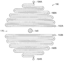
도 1은 본 교시에 따른 멀티 챔버 CVD 시스템의 일 실시예의 측면도.
도 2a는 기판 캐리어 위로 인클로저를 이동시킴으로써 증착 챔버가 형성되는 본 교시에 따른 증착 챔버의 일 실시예의 측면도.
도 2b는 기판 캐리어를 인클로저 내로 이동시킴으로써 증착 챔버가 형성되는 본 교시에 따른 증착 챔버의 일 실시예의 측면도.
도 3a, 3b, 3c, 3d는 본 시스템에서 유용한 가열기들의 서로 다른 실시예들을 도시하는 도.
도 4는 특정한 모드에 있는 도 1의 멀티 챔버 CVD 시스템의 실시예의 측면도.
도 5는 다른 특정한 모드에 있는 도 1의 멀티 챔버 CVD 시스템의 실시예의 측면도.
도 6은 또 다른 특정한 모드에 있는 본 교시에 따른 멀티 챔버 CVD 시스템의 실시예의 측면도.
도 7a는 공정 가스들이 증착 챔버 내로 수평으로 주입되는 본 교시에 따른 증착 챔버의 일 실시예의 측면도.
도 7b는 도 7a에 도시한 증착 챔버의 (A 방향으로의) 탑다운도(top-down view).
도 8은 본 교시에 따른 수평 흐름 가스 주입기 CVD 시스템의 다른 변형예의 상측 사시도.
도 9는 본 교시에 따른 수평 흐름 가스 주입기 CVD 시스템의 또 다른 변형예의 측면도.The present teachings and additional advantages in accordance with the preferred and illustrative embodiments are described in more detail in the following detailed description in conjunction with the accompanying drawings. Those skilled in the art will appreciate that the figures described below are for illustration only. The drawings are not necessarily to scale, and are illustrated to emphasize the principles of the present teachings. The drawings are not intended to limit the applicant's teaching scope in any way.
1 is a side view of an embodiment of a multi-chamber CVD system according to the present teachings.
2A is a side view of one embodiment of a deposition chamber according to the present teachings in which a deposition chamber is formed by moving an enclosure above a substrate carrier.
Figure 2B is a side view of one embodiment of a deposition chamber according to the present teachings in which a deposition chamber is formed by moving a substrate carrier into an enclosure.
Figures 3a, 3b, 3c, 3d show different embodiments of heaters useful in the present system.
Figure 4 is a side view of an embodiment of the multi-chamber CVD system of Figure 1 in a particular mode.
Figure 5 is a side view of an embodiment of the multi-chamber CVD system of Figure 1 in another specific mode.
6 is a side view of an embodiment of a multi-chamber CVD system in accordance with the present teachings in yet another particular mode.
7A is a side view of one embodiment of a deposition chamber according to the present teachings in which process gases are injected horizontally into a deposition chamber.
FIG. 7B is a top-down view (in the A direction) of the deposition chamber shown in FIG. 7A. FIG.
8 is a top perspective view of another variant of a horizontal flow gas injector CVD system according to the present teachings.
Figure 9 is a side view of another variant of a horizontal flow gas injector CVD system according to the present teachings.
명세서에서 "일 실시예" 또는 "한 실시예"라는 것은, 실시예와 함께 설명하는 구체적인 특징부, 구조, 또는 특징이 본 교시의 하나 이상의 실시예에 포함된다는 것을 의미한다. 본 명세서의 다양한 위치에서 보이는 "일 실시예에서"라는 구는 반드시 동일한 실시예를 가리키는 것은 아니다.In the specification, "one embodiment" or "an embodiment" means that a particular feature, structure, or characteristic described in connection with the embodiment is included in one or more embodiments of the present teachings. The phrase "in one embodiment" in various places in the specification is not necessarily referring to the same embodiment.
본 교시의 방법의 개별적인 단계들은 본 교시를 실시할 수 있는 한 임의의 순서 및/또는 동시에 수행될 수 있다는 점을 이해하기 바란다. 또한, 본 교시의 장치와 방법은 본 교시를 실시할 수 있는 한 설명한 실시예들의 임의의 개수 또는 모두를 포함할 수 있다는 점을 이해하기 바란다.It is to be understood that the individual steps of the method of the present teachings may be performed in any order and / or concurrently as long as the teachings can be practiced. It is also to be understood that the devices and methods of the present teachings can include any number or all of the described embodiments as long as the teachings herein can be practiced.
이제, 첨부 도면에 도시한 바와 같이 본 교시의 예시적인 실시예들을 참조하여 본 교시를 더욱 상세히 설명한다. 본 교시를 다양한 실시예들 및 예들과 함께 설명하지만, 본 교시를 이러한 실시예들로 한정하려는 것은 아니다. 오히려, 본 교시는, 당업자가 인식하듯이, 다양한 대안들, 수정예들, 균등물들을 포함한다. 당업자라면, 본 명세서에서 설명하는 바와 같이 본 명세서의 범위 내에 있는 다른 사용 분야들뿐만 아니라 추가 구현예들, 수정예들, 및 실시예들도 인식할 것이다.The present teaching will now be described in more detail with reference to exemplary embodiments of the present teachings, as shown in the accompanying drawings. Although the present teachings are described in conjunction with various embodiments and examples, it is not intended to limit the present teachings to such teachings. Rather, the teachings, as recognized by those skilled in the art, include various alternatives, modifications, and equivalents. Those skilled in the art will recognize additional embodiments, modifications, and embodiments as well as other fields of use within the scope of the present disclosure as described herein.
본 교시는 CVD, MOCVD, HVPE 등의 반응 가스 위상 처리를 위한 방법과 장치에 관한 것이다. 반도체 재료의 반응 가스 위상 처리에 있어서, 반도체 기판 또는 기판은 반응 챔버 내의 기판 캐리어에 장착된다. 가스 분배 주입기 또는 주입기 헤드는 기판 캐리어를 향하여 장착된다. 주입기 또는 주입기 헤드는 통상적으로 가스들의 조합을 수용하는 복수의 가스 입구를 포함한다. 주입기 또는 주입기 헤드는 화학적 기상 증착을 위한 반응 챔버 내로 가스들의 조합을 제공한다. 많은 가스 분배 주입기들은 헤드 상에 패턴으로 이격된 샤워헤드 디바이스들을 갖는다. 가스 분배 주입기들은, 전구체 가스들이 기판들에 가능한 가까워질수록 반응하고 이에 따라 기판 표면에서의 반응 공정들과 에피택셜 성장을 최대화하도록 기판 캐리어에서의 전구체 가스들을 제어한다.The present teachings relate to methods and apparatus for the treatment of reactive gas phases such as CVD, MOCVD, HVPE, and the like. In the reactive gas phase processing of the semiconductor material, the semiconductor substrate or the substrate is mounted to the substrate carrier in the reaction chamber. A gas distribution injector or injector head is mounted toward the substrate carrier. The injector or injector head typically includes a plurality of gas inlets that accept a combination of gases. The injector or injector head provides a combination of gases into the reaction chamber for chemical vapor deposition. Many gas distribution injectors have showerhead devices spaced apart in a pattern on the head. The gas distribution injectors react with the precursor gases as close to the substrates as possible and thus control the precursor gases in the substrate carrier to maximize reaction processes and epitaxial growth at the substrate surface.
일부 가스 분배 주입기들은, 화학적 기상 증착 공정(CVD Process) 동안 가스 층류(laminar gas flow)를 제공하는 것을 보조하는 슈라우드(shroud)를 제공한다. 또한, 하나 이상의 캐리어 가스(carrier gases)는 화학적 기상 증착 공정 동안 가스 층류를 제공하는 것을 보조하는 데 사용될 수 있다. 캐리어 가스는, 통상적으로, 어떠한 공정 가스(process gases)들과도 반응하지 않으며, 그 외에는 화학적 기상 증착 공정에 영향을 끼치지 않는다. 가스 분배 주입기는, 통상적으로, 전구체 가스들을 주입기의 가스 입구들로부터 기판들이 처리되는 반응 챔버의 소정의 타겟 영역들로 향하게 한다.Some gas distribution injectors provide a shroud that assists in providing laminar gas flow during a Chemical Vapor Deposition process (CVD Process). In addition, one or more carrier gases may be used to assist in providing gas laminar flow during the chemical vapor deposition process. Carrier gases typically do not react with any process gases and do not otherwise affect the chemical vapor deposition process. A gas distribution injector typically directs precursor gases from the gas inlets of the injector to certain target areas of the reaction chamber in which the substrates are to be processed.
예를 들어, MOCVD 공정에 있어서, 주입기는 암모니아나 아르신 등의 금속 유기물들과 수소화물들을 포함하는 전구체 가스들의 조합을 주입기를 통해 반응 챔버 내에 도입한다. 수소, 질소 등의 캐리어 가스, 또는 아르곤 또는 헬륨 등의 불활성 가스는 기판 캐리어에서의 층류(laminar flow)를 유지하는 것을 보조하도록 주입기를 통해 반응 장치 내로 종종 도입된다. 전구체 가스들은 반응 챔버 내에서 혼합되고 반응하여 기판 상에 막을 형성한다. GaAs, GaN, GaAlAs, InGaAsSb, InP, ZnSe, ZnTe, HgCdTe, InAsSbP, InGaN, AlGaN, SiGe, SiC, ZnO, InGaAlP 등의 많은 화합물 반도체들은 MOCVD에 의해 성장되었다.For example, in a MOCVD process, the injector introduces a combination of precursor gases, including metal organics and hydrides, such as ammonia or arsine, into the reaction chamber through an injector. Carrier gases such as hydrogen, nitrogen, or inert gases such as argon or helium are often introduced into the reactor through an injector to assist in maintaining the laminar flow in the substrate carrier. The precursor gases are mixed and reacted in the reaction chamber to form a film on the substrate. Many compound semiconductors such as GaAs, GaN, GaAlAs, InGaAsSb, InP, ZnSe, ZnTe, HgCdTe, InAsSbP, InGaN, AlGaN, SiGe, SiC, ZnO and InGaAlP were grown by MOCVD.
MOCVD와 HVPE 공정 모두에 있어서, 기판은 반응 챔버 내에서 상승된 온도에서 유지된다. 공정 가스들은 통상적으로 반응 챔버 내에 도입되면 약 50 내지 60℃ 이하의 비교적 저온에서 유지된다. 공정 가스들이 고온 기판에 도달하면, 공정 가스들의 온도 및 이에 따른 반응을 위해 이용가능한 에너지가 증가한다.In both the MOCVD and HVPE processes, the substrate is maintained at an elevated temperature in the reaction chamber. Process gases are typically maintained at relatively low temperatures of about 50 to 60 캜 when introduced into the reaction chamber. As the process gases reach the high temperature substrate, the temperature and the energy available for reaction to the process gases increases.
CVD 반응 장치의 가장 흔한 유형은 회전형 디스크 반응 장치이다. 이러한 반응 장치는 통상적으로 디스크형 기판 캐리어를 사용한다. 기판 캐리어는 취급할 하나 이상의 기판을 유지하도록 배열된 포켓들 또는 다른 특징부들을 갖는다. 캐리어는, 캐리어 상에 위치하는 기판들과 함께, 반응 챔버 내에 배치되며, 캐리어의 기판 담지면이 상류 방향으로 향하도록 유지된다. 캐리어는, 통상적으로 상류에서 하류로 향하는 방향으로 연장되는 축을 중심으로 분당 수백 회전의 회전 속도로 회전된다. 기판 캐리어의 회전은 증착된 반도체 재료의 균일성을 개선한다. 기판 캐리어는, 이 공정 동안 약 350℃ 내지 약 1600℃ 범위일 수 있는 소망하는 상승된 온도에서 유지된다.The most common type of CVD reactor is a rotary disk reactor. Such a reactor typically uses a disk-shaped substrate carrier. The substrate carrier has pockets or other features arranged to hold one or more substrates to be handled. The carrier is disposed in the reaction chamber together with the substrates positioned on the carrier, and the substrate-supporting surface of the carrier is maintained to be directed in the upstream direction. The carrier is typically rotated at a rotational speed of several hundred revolutions per minute about an axis extending in the direction from upstream to downstream. Rotation of the substrate carrier improves the uniformity of the deposited semiconductor material. The substrate carrier is maintained at the desired elevated temperature, which may range from about 350 [deg.] C to about 1600 [deg.] C during this process.
캐리어가 축을 중심으로 회전하는 동안, 반응 가스들이 캐리어 위의 흐름 입구 요소로부터 챔버 내로 도입된다. 흐르는 가스들은 바람직하게 마개 층류(laminar plug flow)로 캐리어와 기판들을 향하여 하향 이동한다. 가스들이 회전하고 있는 캐리어에 접근함에 따라, 점성 저항에 의해 가스들이 축을 중심으로 한 회전 내에 이끌려 캐리어의 표면 근처의 경계 영역에서, 가스들이 캐리어의 경계를 향하여 외측으로 축을 중심으로 흐른다. 가스들이 캐리어의 외측 가장자리 위로 흐름에 따라, 가스들은 캐리어 아래에 위치한 배기 포트들을 향하여 하향으로 흐른다. 가장 흔하게는, MOCVD 공정들은, 서로 다른 가스 조성으로 그리고 일부 경우에는 서로 다른 기판 온도에서 연속적으로 수행되어, 필요에 따라 조성이 서로 다른 반도체의 복수의 층을 증착하여 소망하는 반도체 디바이스를 형성한다.While the carrier rotates about the axis, reaction gases are introduced into the chamber from the flow inlet element on the carrier. The flowing gases preferably move downward toward the carrier and the substrates in a laminar plug flow. As the gases approach the carrier rotating, the gases are attracted by the rotation about the axis by the viscous resistance and the gases flow around the axis outwardly toward the boundary of the carrier, in the boundary region near the surface of the carrier. As the gases flow over the outer edge of the carrier, the gases flow downward toward the exhaust ports located below the carrier. Most often, the MOCVD processes are performed sequentially in different gas compositions and, in some cases, at different substrate temperatures, to deposit a plurality of layers of semiconductors of different compositions, if desired, to form the desired semiconductor device.
CVD 또는 MOCVD 반응 장치의 다른 유형으로는, 증착 및/또는 에피택셜층 성장 동안 반응 장치 내에서 회전하지 않는 디스크형 기판 캐리어들이 있다.Other types of CVD or MOCVD reaction devices include disc-shaped substrate carriers that do not rotate in the reactor during deposition and / or epitaxial layer growth.
본 교시의 장치와 방법은 선형 및 인라인 CVD 처리 시스템(CVD processing system)에 관한 것이다. 기판 수송과 관련하여 본 명세서에서 사용되는 바와 같은 "인라인"이라는 용어는 멀티 챔버 CVD 시스템의 한 챔버로부터 멀티 챔버 CVD 시스템의 다른 한 챔버로의 평면에서의 기판 수송을 가리킨다. 인라인 수송은 직선에서는 필요하지 않은 수송이다. 수송은 선형일 수 있고 또는 곡선을 따른 것일 수도 있다. 예를 들어, 상업적으로 이용가능한 인라인 시스템들은 여러 평행 라인들로, 원형으로, U 형상으로 배치되어 있으며, 또는 선형 또는 U 형상 구성으로 수직으로 적층된다. 또한, 수송은 동일한 시작점과 종료점을 갖는 폐쇄된 레일이나 트랙을 따른 것일 수 있고, 또는 한 방향으로만 향한 것일 수도 있다. 본 교시에 따른 수송 기구를 가리키는 경우의 "인라인"이라는 용어는, 두 개 이상의 롤러 주위로 회전하는 연속 벨트와 함께 그 두 개 이상의 롤러를 포함하는 컨베이어 벨트 등의 컨베이어형 수송 기구를 포함할 수 있다. 본 발명에서 유용한 시스템 처리 아키텍처(architectures)들의 다른 유형들은 ""System for Fabricating a Pattern on Magnetic Recording Media"라는 명칭으로 2009년 8월 26일자로 가출원한 미국 특허 가출원번호 제61/237,141호에서 찾을 수 있으며, 그 전문은 본 명세서에 참고로 원용된다.The apparatus and method of the present teachings relates to a linear and in-line CVD processing system. The term "in-line " as used herein in reference to substrate transport refers to substrate transport in a plane from one chamber of a multi-chamber CVD system to another chamber of a multi-chamber CVD system. Inline transport is a transport that is not needed in a straight line. The transport may be linear or may be along a curve. For example, commercially available inline systems are arranged in several parallel lines, circular, U-shaped, or vertically stacked in a linear or U-shaped configuration. The transport may also be along a closed rail or track with the same starting and ending points, or may be directed in one direction only. The term "in-line" when referring to a transport mechanism according to the present teachings may include a conveyor-type transport mechanism, such as a conveyor belt, that includes two or more rollers with a continuous belt rotating about two or more rollers . Other types of system processing architectures useful in the present invention can be found in U.S. Provisional Patent Application Serial No. 61 / 237,141, filed August 26, 2009, entitled "System for Fabricating a Pattern on Magnetic Recording Media & , The disclosure of which is incorporated herein by reference.
MOCVD와 HVPE 등의 CVD를 위한 알려져 있는 장치와 방법은 선형 및 인라인 처리 시스템에 적합하지 않다. 본 교시의 장치와 방법은 MOCVD와 HVPE 등의 CVD의 임의의 유형을 수행할 수 있다. 본 교시의 일 양태에서, 본 교시의 장치와 방법은 인라인 불연속 수송 기구를 사용한다. 본 명세서에서 언급하는 바와 같은 "불연속 수송 기구"라는 용어는 비연속적 스텝으로 기판들 및/또는 기판 캐리어들을 수송하는 수송 기구이다. 즉, 기판들 및/또는 기판 캐리어들은 멀티 챔버 CVD 처리 시스템의 하나의 CVD 처리 챔버로부터 그 멀티 챔버 CVD 처리 시스템의 다른 하나의 CVD 처리 챔버로 수송된 후, CVD 공정 단계가 수행되는 동안 미리 정해진 시간 동안 고정 위치에서 각자의 CVD 공정 챔버 내에 위치한다.Known devices and methods for CVD such as MOCVD and HVPE are not suitable for linear and inline processing systems. The apparatus and method of the present teachings can perform any type of CVD, such as MOCVD and HVPE. In one aspect of the present teachings, the apparatus and method of the present teachings use inline discrete transport mechanisms. The term "discontinuous transport mechanism " as referred to herein is a transport mechanism for transporting substrates and / or substrate carriers in discontinuous steps. That is, the substrates and / or substrate carriers are transported from one CVD processing chamber of a multi-chamber CVD processing system to another CVD processing chamber of the multi-chamber CVD processing system, and then a predetermined time Lt; RTI ID = 0.0 > CVD < / RTI >
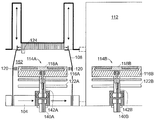
도 1은 본 교시에 따른 멀티 챔버 CVD 시스템(100)의 일 실시예의 측면도를 도시한다. CVD 시스템(100)은 미국 뉴욕주 플레인뷰에 소재하는 Veeco Instruments Inc.에 의해 제조된 자동화 기계적 취급 시스템 등의 기판 로딩 스테이션(102)을 포함한다. 기판 로딩 스테이션(102)은 통상적으로 CVD 처리를 위해 기판들이 삽입되는 기압에 개방되어 있다. 게이트 밸브는 기판 로딩 스테이션(102)을, 멀티 챔버 CVD 시스템(100)의 증착 챔버들(110, 152)을 형성하는 복수의 인클로저(108)를 포함하는 하우징(106) 내에 위치하는 기판 수송 기구(104)의 입력에 인터페이싱(interfacing)한다. 증착 챔버들(110, 152)의 상부에는 가스 흐름 플랜지(300)가 있다. 가스 흐름 플랜지(300)는 통상적으로 MOCVD 또는 CVD 공정 챔버들에서 찾을 수 있는 흐름 입구 요소이다. 이러한 가스 흐름 플랜지는 통상적으로 하나 이상의 반응 가스 소스를 갖고, 일부 경우에는, 캐리어 가스를 갖고, 기판 방향으로 향하는 적절한 가스 흐름을 보장하도록 매니폴드(manifolds), 배플(baffles), 가스 분배 챔버도 갖는다. 적절한 가스 흐름 플랜지의 일례는 미국 특허출원 공개번호 제2010/0143588호에서 알 수 있다. 증착 챔버들(110, 152)의 하부에는, 공정 조건들에 따라 또는 인클로저들(enclosures;108)이 오목부(170) 내로 이동하고 스핀들(140A, 140B)이 시스템(100) 내의 다음 정지부로 병진 운동할 수 있도록 증착 챔버들(110, 152)에서 반응 가스들이 퍼지(purge)되는지에 따라, 증착 챔버들(110, 152)을 가압하거나 배기하도록 적절한 펌프, 가스 소스, 및 배기 매니폴드가 구비될 수 있는 오리피스(160)가 있다. 스핀들(140A, 140B)은, 당업자에게 알려져 있는 다양한 커넥터들에 의해, 예를 들어, 기계적 커넥터(예를 들어, 너트와 볼트), 전자기계적 커넥터(예를 들어, 솔레노이드 핀), 자기 결합에 의해 기판 수송 시스템(104)에 연결될 수 있지만, 이러한 예로 한정되지는 않는다. 본 명세서에서 설명하는 다른 기판 수송 시스템과 스핀들도 마찬가지 방식으로 연결될 수 있다.1 illustrates a side view of one embodiment of a
처리된 기판들은, 복수의 인클로저(108)를 포함하는 하우징(106)의 단부에 위치하는 기판 언로딩 스테이션(substrate unloading station; 112)에 의해 멀티 챔버 CVD 시스템(100)으로부터 제거된다. 기판 언로딩 스테이션(112)은 미국 뉴욕주 플레인뷰에 소재하는 Veeco Instruments Inc.에 의해 제조된 자동화 기계적 취급 시스템일 수도 있다. 기판 언로딩 스테이션(112)은 통상적으로 CVD 처리 후에 기판들이 제거되는 기압에 개방되어 있다. 게이트 밸브는, 기판 언로딩 스테이션(112)을, 멀티 챔버 CVD 시스템(100)의 증착 챔버들(110, 152)을 형성하는 복수의 인클로저(108)를 포함하는 하우징(106) 내에 위치하는 기판 수송 기구(104)의 출력에 인터페이싱한다. 기판 로딩 스테이션(substrate loading station; 102)과 기판 언로딩 스테이션(112) 모두는 또한 시스템의 나머지 부분과는 독립적인 펌프 퍼지형일 수 있다.The processed substrates are removed from the
수송 기구(104)를 따라 이동가능한 복수의 기판 캐리어(114A, 114B)가 존재한다. 도 1에 도시한 멀티 챔버 CVD 시스템은 도면을 간략화하도록 두 개의 기판 캐리어만 도시하고 있다. 실제로, 본 교시에 따른 멀티 챔버 CVD 시스템은, 수많은 증착 챔버들(110, 152)을 형성하도록 인클로저들(108) 내에 밀폐된 수많은 기판 캐리어들(114A, 114B)을 포함한다. 일부 CVD 시스템들은 기판 상에서 성장된 각 층마다 하나의 증착 챔버를 갖도록 구성된다.There are a plurality of
복수의 기판 캐리어(114A, 114B)는, 기판들이 기판 로딩 스테이션(102)으로부터 인접하는 기판 캐리어들(114A, 114B)로 수송될 수 있도록 기판 로딩 스테이션(102)과 인터페이싱한다. 복수의 기판 캐리어(114A, 114B)의 각각은 서셉터(116A, 116B)와 기판 캐리어 조립체(118A, 118B)를 각각 포함한다. 서셉터(116A, 116B)는, 열적 에너지가 가열기들(122A, 122B)로부터 기판들로 쉽게 전달되도록 고온에서 높은 열 전도성을 갖는 재료로 된 베이스 구조를 포함한다. 기판 캐리어 조립체(118A, 118B)는, CVD에 의한 에피택셜층들의 성장 동안 반도체 웨이퍼 등의 하나 이상의 기판을 유지하기 위한 플래튼(platen), 및 서셉터(116A, 116B)를 지지하는 스핀들(140A, 140B)을 포함하고, 이러한 스핀들은, 본 명세서에서 개시한 바와 같이 일부 경우에는, 예를 들어 단일 지지 폴(pole)일 수 있거나 스핀들(140A, 140B) 주위의 슬리브(sleeve)일 수 있는 가열기 지지부(142A, 142B)에 의해 가열기들(122A, 122B)도 지지한다. 다른 실시예들에서, 서셉터 없는 웨이퍼 캐리어를 서셉터(116A, 116B)와 플래튼 대신에 사용할 수 있고, 이때, 열은 가열기들(122A, 122B)로부터, 열 에너지가 가열기들(122A, 122B)로부터 기판들로 쉽게 전달될 수 있도록 고온에서 높은 열 전도성을 갖는 재료로 형성된 웨이퍼 캐리어의 하부로 직접 전달된다. 서셉터 없는 웨이퍼 캐리어의 한 유형은 미국 특허번호 제6,685,774호에 개시되어 있다. 많은 실시예들에서, 복수의 기판 캐리어(114A, 114B)의 각각은 동시에 처리되는 복수의 기판을 지지하는 플래튼을 포함한다.The plurality of
본 교시에 따른 멀티 챔버 CVD 시스템은, 소망하는 성장 온도를 유지하도록 복수의 증착 챔버(110, 152)의 각각에 위치하는 기판들의 성장 표면에서의 온도를 제어하기 위한 복수의 가열기(122A, 122B)를 포함한다. 복수의 가열기(122A, 122B) 중 하나는 복수의 기판 캐리어(114A, 114B)의 각각과 열적으로 접촉하도록 위치한다. 복수의 증착 챔버(110, 152)의 각각의 성장 표면에서의 온도를 제어하는 데 사용될 수 있는 가열기들의 가능한 많은 유형들이 있다. 가열기들(122A, 122B)은 인클로저들(108)의 내부 및/또는 외부에 위치할 수 있다.The multi-chamber CVD system according to the present teachings includes a plurality of
예를 들어, 복수의 가열기(122A, 122B)는 흑연 가열기 등의 저항성 가열기들일 수 있다. 이러한 가열기들은 통상적으로 복수의 기판 캐리어(114A, 114B)의 각각과 열적 접촉하면서 이러한 기판 캐리어의 각각에 근접하여 증착 챔버들(110, 152) 내에 위치한다. 구체적인 일 실시예에서는, 선형 저항성 가열기들의 3개 뱅크(bank)가, 복수의 기판 캐리어(114A, 114B)를 지지하는 스핀들을 전달하기 위한 갭을 사이에 두는 이등분으로 배치된다. 또한, 복수의 가열기(122A, 122B)는, 복수의 증착 챔버(110, 152)의 기판들의 각각의 성장 표면에 RF 에너지를 전달하는 RF 가열기들일 수 있다. 이러한 가열기들은 인클로저들(108)의 내부 또는 외부에 위치하는 RF 유도 코일들을 갖는다. 예를 들어 석영 램프 등의 램프로부터의 방사 에너지를 가열 또는 온도 프로파일(temperature profile)의 미세 조절에 사용할 수도 있다.For example, the plurality of
본 교시에 따른 일부 멀티 챔버 CVD 시스템은, 복수의 기판 캐리어(114A, 114B)가 복수의 인클로저(108) 내외로 수송될 수 있는 갭 또는 통로를 형성하도록 성형된 고정형 저항성 가열기 요소들을 포함한다. 예를 들어, 구체적인 일 실시예에서, 고정형 저항성 가열기들은, 복수의 인클로저(108)가 복수의 증착 챔버(110, 152)의 내외로 전달되는 통로를 정의하는 두 개의 반원형 가열기 요소들을 정의하도록 형성된다. 통로는, 복수의 기판 캐리어가 수송 기구(104)로 수송될 때 복수의 기판 캐리어(114A, 114B)를 지지하는 스핀들이 두 개의 반원형 가열기 요소들 사이의 통로를 통해 자유롭게 통과할 정도로 넓다.Some multi-chamber CVD systems in accordance with the present teachings include stationary resistive heater elements molded to form gaps or passageways through which a plurality of
본 교시에 따른 다른 멀티 챔버 CVD 시스템은, 복수의 기판 캐리어(114A, 114B)가 복수의 인클로저(108) 내외로 수송되는 갭이나 통로를 정의하도록 성형된 고정형 저항성 가열기 요소들을 포함하는 제1 가열기, 및 기판 캐리어들(114A, 114B)에 부착된 제2 가열기를 포함한다. 이러한 가열기들은 독립적으로 제어가능하다. 기판 캐리어들(114A, 114B)에 부착된 가열기는, 기판들이 다음 증착 챔버로 수송되는 동안 기판들을 가열하거나 기판들의 소망 온도를 유지하는 데 사용될 수 있다. 두 개의 가열기를 사용하여 기판들이 소망 공정 온도를 얻는 데 걸리는 시간을 감소시킴으로써 처리량을 증가시킬 수 있다.Another multi-chamber CVD system according to the present teachings includes a first heater comprising stationary resistive heater elements shaped to define gaps or passages through which a plurality of
도 3a는 스핀들이 통과할 수 있는 두 개의 이등분 사이에 갭을 갖는 가열기(122)의 일례(상면도)를 도시한다. 가열기 요소(130A)와 가열기 요소(130B)는 브랫킷(160A와 162A 및 160B와 162B)에 의해 각각 챔버들(110, 152) 내의 임의의 비이동(non-moving) 표면에 연결된다. 적절한 와이어링 및 기타 가열기 제어부도 적절한 브랫킷을 통과한다. 갭(170)은 스핀들(140A, 140B)이 시스템 내의 서로 다른 챔버들을 통해 병진 운동할 때 스핀들(140A, 140B)이 관통 이동할 수 있을 정도로 충분히 넓다.Figure 3a shows an example (top view) of a
도 3b와 도 3c는 가열기 지지부(142)(도시하지 않음)를 사용하여 스핀들(140)에 연결될 수 있는 가열기(122)의 예들을 도시한다. 도 3b에서, 지지부들(147, 148)은 가열기(122)를 다른 지지부(도시하지 않음)에 연결한다. 적절한 와이어링 및 기타 제어부도 지지부들(147, 148)을 통해 이동할 수 있다. 도 3c에서, 브랫킷(146)은 가열기(122)를 가열기 지지부(도시하지 않음)에 연결하고 이때 적절한 와이어링과 기타 제어부가 가열기 지지부(142)(도시하지 않음)를 통해 브랫킷(146)으로 이동한다.Figures 3b and 3c illustrate examples of the
도 3d는 스핀들이 통과할 수 있는 두 개의 이등분 사이에 갭을 갖는 가열기(190)의 다른 일례(상면도)를 도시한다. 가열기 요소(196A)와 가열기 요소(196B)는 브랫킷들(192A와 194A 및 192B와 194B)에 의해 각각 챔버들(110, 152) 내의 임의의 비이동 표면에 연결된다. 적절한 와이어링과 기타 가열기 제어부도 대응하는 브랫키들을 관통한다. 갭(170)은, 스핀들(140A, 140B)이 시스템 내의 서로 다른 챔버들을 통해 병진 운동할 때 스핀들(140A, 140B)이 관통 이동할 수 있을 정도로 충분히 넓다.FIG. 3D shows another example (top view) of
다른 일 실시예에서는, 기판들 자체가 저항성 가열기로서 사용된다. 본 실시예에서, 기판들은, 저항성 가열에 적합한 저항성을 나타내는 두께의 재료로 이루어진다. 전원은 기판들에 전기적으로 연결된다. 전원에 의해 발생하는 전류는 기판들이 소망 처리 온도까지 가열되도록 조정된다. 당업자는, 기판들(104)을 가열하는 데 가열기의 다른 유형들을 사용할 수 있다는 점을 인식할 것이다. 또한, 본 교시에 따른 멀티 챔버 CVD 시스템은, 기판들의 성장 표면을 소망 처리 온도까지 가열하도록 증착 챔버들(110, 152) 내부에 및/또는 외부에 위치할 수 있는 가열기의 다수의 유형들을 포함할 수 있다.In another embodiment, the substrates themselves are used as resistive heaters. In this embodiment, the substrates are made of a material having a thickness that is resistant to resistive heating. The power source is electrically connected to the substrates. The current generated by the power source is adjusted so that the substrates are heated to the desired processing temperature. Those skilled in the art will appreciate that other types of heaters may be used to heat the
본 교시의 일부 실시예들에서, 복수의 기판 캐리어(114A, 114B) 중 하나 이상은 처리 동안 축을 중심으로 하나 이상의 기판을 회전시킨다. 회전 속도는 특정 공정에 의존한다. 일부 공정에서, 회전 속도는 최대 1500rpm에 이른다. 다른 실시예들에서, 복수의 기판 캐리어(114A, 114B) 중 하나 이상은 처리 동안 하나 이상의 기판을 병진 운동시킨다. 또 다른 실시예들에서, 복수의 기판 캐리어(114A, 114B) 중 하나 이상은 처리 동안 하나 이상의 기판을 회전시키고 병진 운동시킨다. 하나 이상의 기판이 그 축을 중심으로 회전하는 플래닛(planet) 상에 로딩되는 동안 기판 캐리어들은 정지 상태를 유지하거나 선형으로 병진 운동할 수도 있다. 기판 캐리어는, 기판들이나 플래닛들이 캐리어 상에 다양한 구성으로 배열되는 둥근형일 수 있고, 또는 캐리어가 회전하지 않는 경우에는 직사각형이나 정사각형일 수 있다. 캐리어 구성은 처리되는 기판 크기에 최적화된다. 이러한 방식으로, 둥근 형상, 정사각형, 또는 직사각형이며 2" 내지 12" 크기의 기판들은 통상적으로 적절한 크기와 구성의 캐리어를 사용함으로써 처리될 수 있다.In some embodiments of the present teachings, at least one of the plurality of
복수의 인클로저(108)의 각각은, 독립적 환경을 유지하도록 복수의 기판 캐리어(114A, 114B) 중 하나를 밀폐하는 복수의 증착 챔버(110, 152) 중 하나를 형성하도록 구성된다. 독립적 환경에서, 화학적 기상 증착 공정의 화학적 반응은 CVD 처리 단계로서 수행될 수 있다. 독립적 환경의 다른 예에서는, 어닐링 또는 다른 비화학적 기상 증착 공정의 화학적 반응 단계들이 수행될 수 있다. 본 교시에 따른 일부 시스템에서, 복수의 증착 챔버(110, 152)의 각각은 CVD 처리 단계들의 순서로 복수의 처리 단계들 중 하나를 수행하도록 설계되고 작동된다. 본 교시에 따른 다른 시스템에서, 복수의 증착 챔버(110, 152)의 각각은, 관련된 화학적 기상 증착 공정의 화학적 반응일 수 있고 아닐 수도 있는 하나 이상의 처리 단계를 수행한다.Each of the plurality of
많은 실시예들에서, 복수의 인클로저(108) 중 하나 이상은 스테인레스 스틸 인클로저 또는 글래스 벨 자(glass bell jar) 등의 물리적 인클로저를 포함한다. 당업자라면, 많은 유형의 재료를 사용하여 물리적 인클로저를 형성할 수 있음을 인식할 것이다. 많은 실시예들에서, 복수의 인클로저(108)의 각각은 증착 동안 발생하는 열을 제거하도록 유체 냉각된다. 물 또는 다른 유형의 유체를 쿨링하기 위한 도관들은 복수의 인클로저(108) 내에 또는 복수의 인클로저 주위에 형성될 수 있다.In many embodiments, one or more of the plurality of
다른 실시예들에서, 복수의 인클로저(108) 중 하나 이상은 대응하는 인클로저의 하나 이상의 경계를 형성하는 가스 커튼(또는 퍼지)을 포함한다. 이러한 실시예들에서, 인접하는 가스 커튼들은 진공 하의 영역에 의해 분리될 수 있다. 진공 하에 있는 영역들은, 분리된 공정 화학 반응들이 복수의 증착 챔버들(110, 152)의 각각 내에서 유지되도록 인접하는 증착 챔버들(110, 152) 사이의 공정 가스들을 제거한다. 가스 커튼(퍼지)은 통상적인 GaN형 반응 장치를 위한 H2, N2, NH3 및/또는 이들의 임의의 조합일 수 있다. 다른 III/V족 반응 장치를 위해서는, 수소화물 등의 가스(예를 들어, AsH3 또는 PH3)가 유용하다. 인클로저들 간의 공정 누화를 감소시키기 위해, 인클로저 내의 압력은 인클로저가 개방되기 전에 전체 챔버의 압력으로 평형화된다. 또한, 가스들은 캐리어가 하나의 스테이션으로부터 다른 하나의 스테이션으로 수송되고 있는 동안 원치 않는 기판 열화를 방지하는 데 필요한 가스 분위기를 유지하도록 각 주입기 내에 위치하는 선택된 주입기들을 통해 계속해서 흐를 수 있다.In other embodiments, at least one of the plurality of
다른 실시예들에서, 하나 이상의 가스 커튼들은 복수의 인클로저(108) 중 두 개 이상 사이에서 사용된다. 이러한 가스 커튼은, 복수의 증착 챔버(110, 152)의 각각 내에서 공정 화학적 반응들이 개별적으로 유지되도록 하나의 증착 챔버에서 사용되는 공정 가스들이 다른 하나의 증착 챔버에 유입되는 것을 방지하는 데 사용될 수 있다. 또 다른 실시예들에서, 가스 퍼지는 복수의 증착 챔버(110, 152) 중 두 개 이상 간의 영역들에서 사용될 수 있다. 가스 퍼지는, 잔여 공정 가스들이 가스 퍼지를 통해 다음 증착 챔버로 이동할 때 기판들로부터 그 잔여 공정 가스들을 제거하는 데 사용될 수 있다.In other embodiments, one or more gas curtains are used between two or more of the plurality of
인클로저들은 작동 모드에 따라 동기식으로 또는 비동기식으로 작동할 수 있다. 캐스케이드 모드에서, 캐리어는, 최종 스테이션으로부터의 캐리어가 제거된 후 최종 스테이션으로 이동할 수 있고, 공정이 스테이션들을 통해 진행된다. 다른 모드에서는, 모든 캐리어들이 하나의 스테이션으로부터 다른 하나의 스테이션으로 동기식으로 이동한다. 또 다른 모드에서는, 최종 스테이션이 언로딩되고, 이어서, 나머지 캐리어들이 다음 스테이션으로 동기식으로 연동된다. 캐리어들이 챔버들 간에 양방향으로 이동할 수 있는 다른 작동 모드들도 가능하며, 이에 따라 성장의 한 부분을 완료하는 데 연속되는 챔버들의 한 세트를 사용하는 한편 그 성장의 다른 한 부분을 완료하는 데 그 연속되는 챔버들의 다른 한 세트를 사용한다. 최적의 작동 모드는 공정과 처리량에 종속되는 것이다.Enclosures can operate synchronously or asynchronously depending on the mode of operation. In cascade mode, the carrier can move to the last station after the carrier from the last station is removed, and the process proceeds through the stations. In another mode, all carriers move synchronously from one station to another. In another mode, the last station is unloaded, and then the remaining carriers are synchronously interlocked to the next station. Other modes of operation in which the carriers can move in both directions between the chambers are also possible, thus using one set of successive chambers to complete a part of growth while continuing to successively complete another part of the growth Lt; RTI ID = 0.0 > chambers. ≪ / RTI > The optimal mode of operation is dependent on process and throughput.
복수의 인클로저의 각각은, 하나 이상의 가스 입력 포트가 하나 이상의 공정 가스를 각 증착 챔버들(110, 152) 내에 주입하도록 하나 이상의 CVD 공정 가스 소스에 결합된 그 하나 이상의 가스 입력 포트를 포함한다. 가스 흐름 플랜지(300)(도 2a와 도 2b)는, 본 교시에 따른 멀티 챔버 CVD 시스템과 함께 사용될 수 있는, 75℃를 넘는 온도에서 CVD 공정 가스들을 주입하는 데 사용될 수 있는 상승된 온도 가스 입력 포트들을 포함한 다수의 가스 입력 포트를 포함할 수 있다. 증착 챔버들(110, 152)의 벽들은 가스 입력 포트 온도 또는 가스 입력 포트 온도를 초과하는 온도로 가열될 수 있다. 상승된 가스 입력 포트 온도를 사용함으로써, 비교적 느린 기판 캐리어 회전 속도, 비교적 높은 작동 압력, 비교적 느린 유속, 또는 바람직한 기판 캐리어 회전 속도, 작동 압력, 가스 유속의 일부 조합을 사용할 수 있다. 각 인클로저 내에서 흐름 플랜지의 다른 구성을 이용할 수도 있다. 예를 들어, 다른 구성은, 디스크 반응 장치를 회전시키도록 구성된 흐름 플랜지, 밀착 결합된 샤워헤드 반응 장치, 교차 흐름 행성 운동형 반응 장치, 공간적 또는 시간 변조형 원자층 에피택시 반응 장치, 플라즈마, 또는 핫 와이어 CVD 반응 장치를 포함할 수 있다. 일반적으로, 인라인 구현예와 호환성 있는 임의의 반응 장치 유형을 사용할 수 있다. 이는, 특정한 성장 단계를 위해 가장 적합한 반응 장치 구성이 사용되는 맞춤(mix and match) 전략을 가능하게 한다. 본 발명에서 유용한 반응 장치 설계와 기판 캐리어 설계의 다른 유형은, "Metal-Organic Vapor Phase Epitaxy System and Process"라는 명칭으로 2011년 4월 7일자로 가출원한 미국 특허 가출원번호 제61/472,925호에서 찾을 수 있는 것들을 포함하며, 그 전문은 본 명세서에 참고로 원용된다.Each of the plurality of enclosures includes one or more gas input ports thereof coupled to one or more CVD process gas sources such that the one or more gas input ports inject one or more process gases into each of the deposition chambers 110,152. The gas flow flange 300 (FIGS. 2A and 2B) includes an elevated temperature gas input that can be used to inject CVD process gases at temperatures in excess of 75 DEG C, which can be used with the multi-chamber CVD system according to the present teachings And may include a plurality of gas input ports including ports. The walls of the
CVD 공정 가스들은 멀티 챔버 CVD 시스템(100)에 근접하여 위치할 수 있고, 또는 원격 위치에 있을 수도 있다. 많은 실시예들에서, MOCVD 가스 소스 등의 복수의 CVD 가스 소스들은, 가스 분배 매니폴드를 통해 복수의 증착 챔버(110, 152)의 각각의 가스 입력 포트들에 연결되도록 이용가능하다. 멀티 챔버 CVD 시스템(100)은 가스 분배 매니폴드를 구성함으로써 증착되는 재료 구조를 변경하도록 쉽게 구성될 수 있다. 가스 분배 매니폴드는 매니폴드에서 수동으로 구성될 수 있고 또는 전기적으로 작동하는 밸브와 솔레노이드를 활성화함으로써 원격으로 구성될 수 있다. 이러한 장치는, 증착되는 재료 구조를 변경하도록 쉽게 재구성되기 때문에, 연구와 유연성 있는 제조 환경에 매우 적합하다. 모든 증착 챔버들을 위한 소스 가스들을 제공하는 공유 조립체는 부품 카운트와 비용을 감소시키는 한편 모든 챔버들에 전달되는 소스 가스의 일관성을 개선한다. 이러한 조립체는 또한 인라인 정화 장치와 필터 등의 고가 부품들을 공유할 수 있게 한다. 또한, 시스템은 스테이션들 중 하나가 고장 나는 경우에 여분의 스테이션으로서 사용될 수 있는 소스 가스들로 충분히 구성된 여분의 스테이션을 포함할 수 있다. 여분의 스테이션은 시스템 내로 현재 로딩된 기판들 상에서의 모든 공정 단계들의 완료를 가능하게 한다. 재공품(WIP)이 세척된 후, 영향을 받은 스테이션이 서비스를 받을 수 있다. 수송 시스템은 고장 난 스테이션을 우회하는 수단을 포함할 수 있다. 스테이션들 중 하나가 고장 난 경우에 WIP를 복구하는 데 사용되는 알려져 있는 다른 많은 시스템 아키텍처 특징부들이 이 시스템에서 구현될 수 있다.The CVD process gases may be located in close proximity to the
가스 입력 포트들은, CVD 가스들이 복수의 기판의 표면에 도달할 때까지 CVD 가스들이 반응하는 것을 실질적으로 방지하는 가스 분배 노즐을 포함할 수 있다. 이러한 가스 분배 노즐은 공정 가스의 반응들이 증착 챔버들(110, 152) 내의 복수의 기판의 표면으로부터 멀어지면서 발생하는 것을 실질적으로 방지하고 이에 따라 처리되고 있는 기판의 표면 상에 증착된 재료 내에 반응 부산물이 매입되는 것을 방지하도록 구성된다. The gas input ports may include gas distribution nozzles that substantially prevent CVD gases from reacting until the CVD gases reach the surface of the plurality of substrates. These gas distribution nozzles substantially prevent reactions of the process gases from arising away from the surfaces of the plurality of substrates in the
또한, 복수의 인클로저(108)의 각각은 공정 가스들과 반응 부산물 가스들을 제거하기 위한 하나 이상의 배기 포트를 포함한다. 일 실시예에서, 링 형상의 배기 포트(120)는 공정 가스들과 반응 부산물 가스들을 제거하는 데 사용된다. 하나 이상의 배기 포트(120)는 배기 매니폴드에 결합된다. 진공 펌프는 배기 매니폴드에 결합된다. 진공 펌프는 배기 매니폴드를 배기하고, 이에 따라 복수의 증착 챔버(110, 152)로부터 공정 가스들과 반응 부산물 가스들을 제거하는 압력 차를 생성한다. 배기 포트들은 또한 공정 가스의 반응들이 증착 챔버들(110, 152) 내의 기판들의 표면으로부터 멀어지면서 반응하는 것을 실질적으로 방지하고 이에 따라 증착된 막의 오염을 방지하도록 구성된다. 각 챔버마다의 가스 로딩에 따라, 누화가 없고 배기되고 있는 가스들이 서로 호환가능하다면, 배기 펌프들은 또한 다수의 챔버들에 걸쳐 공유될 수 있다.In addition, each of the plurality of
수송 기구(104)는, 미리 정해진 시간 동안 복수의 인클로저(108)의 각각에서 하나 이상의 처리 단계들이 수행될 수 있게 하는 이산적인 스텝으로 복수의 기판 캐리어(114A, 114B)의 각각을 복수의 인클로저(108)의 각각으로 수송한다. 본 교시에 따른 수송 기구의 유형과 이산적인 스텝으로 복수의 증착 챔버(110, 152) 간에 복수의 기판 캐리어(114A, 114B)를 수송하기 위한 많은 수단들이 있다. 예를 들어, 본 교시에 따른 수송 기구의 한 유형은 복수의 기판 캐리어(114A, 114B)의 각각을 레일을 따라 복수의 인클로저(108)의 각각으로 수송한다. 본 교시에 따른 수송 기구의 다른 한 유형은 복수의 기판 캐리어(114A, 114B)의 각각을 트랙 상에서 복수의 인클로저(108)의 각각으로 수송한다. 본 교시에 따른 수송 기구의 또 다른 한 유형은, 복수의 기판 캐리어(114A, 114B)의 각각을, 예를 들어, 컨베이어 벨트를 사용하는 컨베이어 유형 수송 기구에 의해 복수의 인클로저(108)의 각각으로 수송한다. 이러한 수송 시스템에서, 벨트, 푸시로드, 및 자기 선형 모터 등의 자기적으로 결합된 드라이브를 포함할 수 있는 컨베이어 시스템, 레일, 또는 트랙은 복수의 가열기(122A, 122B)에 전력을 제공하도록 설계될 수 있다. 또한, 이러한 수송 시스템에서, 기판 캐리어들(114A, 114B)을 위한 회전 및/또는 병진 운동 조립체 등의 공압 작동식 부품들을 위한 가스는 레일, 트랙, 또는 컨베이어 시스템으로부터 제공될 수 있다.The
도 1에 도시한 수송 기구(104)는 제1 인클로저로부터 제2 인클로저로의 경로로 기판 캐리어들(114A, 114B)을 이동시킨다. 실제로, 통상적으로는, 2개보다 많은 증착 챔버(110, 152)를 형성하는 2개보다 많은 기판 캐리어(114A, 114B)와 인클로저(108)가 존재한다. 다양한 실시예들에서, 수송 기구(104)는 기판 캐리어들을 직선 방향으로 또는 곡선 방향으로 수송할 수 있다. 수송 기구가 복수의 기판 캐리어(114A, 114B)를 수송하는 경로는 시작과 종료가 서로 다른 물리적 위치에 있는 개방 경로 또는 시작 위치와 종료 위치 사이의 직선이나 곡선 경로일 수 있다. 대안으로, 수송 기구(104)가 복수의 기판 캐리어(114A, 114B)를 수송하는 경로는 경로의 종료점이 단일 위치에서의 시작점으로 복귀되는 폐쇄 경로일 수 있다. 다양한 실시예들에서, 폐쇄 경로는, 예를 들어, 원형, 타원형, 또는 연속 트랙(예를 들어, 탱크 트레드(tank tread)) 형상 등의 비선형 경로일 수 있지만, 이러한 예로 한정되지는 않는다.The
많은 실시예들에서, 수송 기구(104)는 한 방향으로 멀티 챔버 CVD 증착 시스템을 통해 기판 캐리어들(114A, 114B)을 수송한다. 그러나, 다른 실시예들에서, 수송 기구는, 제1 방향으로 멀티 챔버 CVD 증착 시스템을 통해 기판 캐리어들(114A, 114B)을 수송한 후 제1 방향의 반대인 제2 방향으로 다시 멀티 챔버 CVD 증착 시스템을 통해 수송한다.In many embodiments, the
도 1에 도시한 실시예에서는, 처리를 위해 기판들을 멀티 챔버 CVD 시스템(100) 내로 삽입하기 위한 한 개의 기판 로딩/언로딩 스테이션(102) 및 처리 후 처리된 기판들을 멀티 챔버 CVD 시스템(100)으로부터 제거하기 위한 다른 한 개의 기판 로딩/언로딩 스테이션(112)이 있다. 처리를 위해 기판들을 멀티 챔버 CVD 시스템(100) 내로 삽입하고 처리 후 멀티 챔버 CVD 시스템(100)으로부터 처리된 기판들을 제거하는 폐쇄 경로를 포함하는 본 교시에 따른 멀티 챔버 CVD 시스템(100)에서는, 단일 기판 로딩/언도링 스테이션이 존재할 수 있다. 많은 실시예들에서, 기판 로딩/언로딩 스테이션(102, 112)으로부터의 기판 취급은 로보틱 수송 기구에 의해 자동화된다. 기판 로딩 및 언로딩 스테이션들은, 또한, 공정 요건들에 따라 세척 또는 서비스 제공을 위해 그 시스템으로부터 캐리어들을 제거/추가하도록 기능을 할 수 있다. 예를 들어, As/P계 재료들의 MOCVD 성장을 위해, 세척이 필요하기 전에 캐리어를 여러 번 재사용할 수 있는 한편, 각 증착 사이클 후에는 GaN계 재료의 성장을 위해 세척이 필요하다. 또한, 제거/교체 및/또는 다른 임의의 종류의 조절을 위해 사용자가 플래튼 또는 웨이퍼 캐리어에 액세스할 수 있는 하나 이상의 액세스 스테이션이나 포트가 있을 수 있다.1, one substrate loading /
본 교시에 따른 일부 멀티 챔버 CVD 시스템들은, 기판 캐리어들(114A, 114B)에 밀접하게 위치하며 이 기판 캐리어들과 일체형이며 이에 따라 기판들의 성장 표면과 열적으로 연통하는 가열기들을 포함하는 수송 기구를 포함한다. 이러한 시스템들에서, 가열기들(122A, 122B)은 기판 캐리어들(114A, 114B)과 함께 이동한다. 기판 캐리어들(114A, 114B)과 일체형인 저항성 가열기들을 위한 전력은 수송 기구에 의해 제공될 수 있고 또는 이동가능한 전력 케이블에 의해 제공될 수 있다.Some multi-chamber CVD systems in accordance with the present teachings include a transport mechanism that is closely located to
본 교시에 따른 일부 시스템들에서, 복수의 인클로저 중 하나 이상은 하나 이상의 현장내 측정 디바이스(in-situ measurement device; 124)를 포함한다. 일부 시스템들에서, 복수의 인클로저 중 하나 이상은, 증착 동안 복수의 기판 캐리어(114A, 114B) 상에 위치하는 기판들의 성장 표면에서의 온도를 측정하는 고온계(pyrometer)를 포함할 수 있다. 그 결과로 얻는 온도 측정 결과를 이용하여, 기판들의 표면에서의 소망 성장 온도를 유지하도록 가열기 제어 회로에 피드백을 제공할 수 있다. 또한, 일부 시스템들에서, 복수의 인클로저(110, 152) 중 하나 이상은 증착된 막의 두께 및/또는 성장 속도를 측정하는 반사율계를 포함한다. 반사율계는, 기판의 성장 표면에서의 온도, 공정 가스 유속, 및 증착 챔버들(110, 152) 내의 압력 등의 다양한 증착 파라미터들을 제어하는 피드백 신호를 제공할 수 있다. 추가 현장내 측정 디바이스들(124)은, 예를 들어, 증착 동안 웨이퍼의 곡률을 측정하는 데 사용될 수 있는 휨 측정계(deflectometer), 편광 측정계(ellipsometer), 포토루미네센스 분광계(photoluminescence spectrometer), 반사율계(reflectometer), 결합된 고온계/반사율계(pyrometer/reflectometer), 결합된 휨 측정계/반사율계/온도 도구, 및 일렉트로루미네센스 분광계(electroluminescence spectrometer) 등을 포함하는, 반도체 산업에서 흔히 사용되는 다른 계량 도구들을 포함한다. 결합된 고온계/반사율계는, 예를 들어, 미국 특허번호 제6,349,270호에 개시된 것일 수 있다. 결합된 휨 측정계/반사율계/온도 도구는 Veeco Instruments의 DRT-210 현장내 공정 모니터(in-situ process monitor)로서 이용가능하다.In some systems according to the present teachings, at least one of the plurality of enclosures includes one or more in-situ measurement devices (124). In some systems, one or more of the plurality of enclosures may include a pyrometer that measures the temperature at the growth surface of the substrates positioned on the plurality of
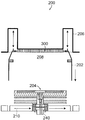
도 2a는 인클로저(202)를 기판 캐리어(204) 위로 이동시킴으로써 증착 챔버(200)가 형성되는 본 교시에 따른 증착 챔버(200)의 일 실시예의 측면도를 도시한다. 본 실시예에서, 기판 캐리어(204)는 수직 방향으로 고정된다. 예를 들어, 기판 캐리어(204)는 트랙, 레일, 또는 컨베이어형 수송 시스템에 부착될 수 있고, 이러한 컨베이어형 수송 시스템은, 또한, (스핀들(240)에 의해 지지되는) 기판 캐리어(204)를 멀티 챔버 증착 시스템(100)(도 1)을 통해 수평 방향으로 수송하는, 벨트, 푸시로드, 및 자기 선형 모터 등의 자기적으로 결합된 드라이브를 포함할 수 있다. 액추에이터(206)는 인클로저(202)를 기판 캐리어(204) 위로 수직 방향으로 병진 이동시켜 증착 챔버(208)를 형성한다. 인클로저(202)는 수송 시스템(210)과 인터페이싱하여 증착 챔버(208) 내의 공정 화학적 반응을 포함하는 밀봉부를 형성한다. 일부 시스템들에서, 수송 시스템(210)은 수송 시스템(104)의 상면 상에 또는 상면 내에 형성된 가스 밀봉부를 포함한다. 구체적인 일 실시예에서, 수송 시스템(210)은, 인클로저(202)의 하부 가장자리가 O-링형 그루브와 직접 접촉하여 O-링, 플랜지, 또는 가스켓을 가압하여 증착 챔버(208) 내에 공정 가스들을 상당히 함유하는 가스 밀봉부를 형성하는 상면 내에 형성된 O-링 그루브를 포함하는 컨베이어형 수송 시스템이다.2A shows a side view of one embodiment of a
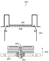
도 2b는, 기판 캐리어(252)를 인클로저(254) 내로 이동시킴으로써 증착 챔버(250)가 형성되는 본 교시에 따른 증착 챔버(250)의 일 실시예의 측면도를 도시한다. 본 실시예에서, 인클로저(254)는 가스 흐름 플랜지(300)에 의해 형성된 천정뿐만 아니라 비이동식 정면, 후면, 및 측벽들로 형성된다. 인클로저(254) 등의 인클로저들은 조립체 영역 내의 다양한 위치에 위치할 수 있고, 수직 및 수평이 되도록 수직 방향과 수평 방향으로 고정된다. 액추에이터(262)는 기판 캐리어(252)가 인클로저(254) 아래에 적절히 정렬될 때까지 기판 캐리어(252)를 수평 방향으로 병진 이동시킨다. 이어서, 액추에이터(256)는 기판 캐리어(252)를 수직 방향으로 인클로저(254) 내로 이동시켜 증착 챔버(258)를 형성한다. 일부 시스템들에서는, 기판 캐리어(252)를 지지하는 스핀들(260)을 수직 방향으로 인클로저(254) 내로 이동시켜 증착 챔버(258)를 형성한다. 이러한 시스템들에서, 수송 시스템(262)은 고정된 위치에 있을 수 있다. 또한, 일부 시스템들에서는, 기판 캐리어(252)를 지지하는 수송 시스템(262)을 수직 방향으로 이동시켜 기판 캐리어(252)를 인클로저(254) 내에 위치시켜 증착 챔버(258)를 형성한다. 인클로저(254)는 수송 시스템(260)과 인터페이싱하여 증착 챔버(258) 내의 공정 화학적 반응을 포함하는 밀봉부를 형성한다. 수송 시스템(260)은, 공정 가스들을 상당히 함유하는 수송 시스템(260)의 상면 상에 또는 상면 내에 형성된, O-링, 플랜지, 또는 가스켓 밀봉부 등의 가스 밀봉부를 포함한다.Figure 2B illustrates a side view of one embodiment of a
다시 도 1을 참조해 보면, 당업자라면, 복수의 인클로저(108)와 복수의 기판 캐리어(114A, 114B)가 인터페이싱하여 복수의 증착 챔버(110, 152)를 형성하는 본 교시에 따른 구성과 복수의 기판 캐리어(114A, 114B)를 밀폐하기 위한 다양한 다른 수단이 있다는 점을 인식할 것이다. 예를 들어, 한 구성에 있어서, 복수의 인클로저(108) 중 하나 이상과 복수의 기판 캐리어(114A, 114B) 중 대응하는 하나가, 복수의 증착 챔버(110, 152) 중 하나 이상을 형성하도록 서로에 대하여 이동가능하다.Referring again to Figure 1, one skilled in the art will appreciate that the configuration according to the present teachings, in which a plurality of
도 4는 인클로저들(108)이 오목부들(170) 내로 상승된 도 1에 도시한 실시예의 측면도를 도시한다. 이렇게 함으로써, 챔버들(110, 152)에서 반응 가스들이 퍼지되었고, 하우징(106) 내의 압력이 균일해졌으며, 이때, 기판 캐리어들(114A, 114B)은 각자의 해당 서셉터(116A, 116B), 기판 캐리어 조립체(118A, 118B), 스핀들(140A, 140B)과 함께, 일부 경우엔, 가열기들(122A, 122B)이 가열기 지지부들(142A, 142B)과 함께, 하우징(106) 내의 수송 기구(104)에 의해 소망하는 공정의 다음 단계로 이동될 수 있다.FIG. 4 shows a side view of the embodiment shown in FIG. 1 in which the
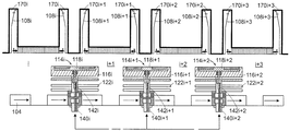
도 5는 다른 특정한 모드에 있는 도 1의 멀티 챔버 CVD 시스템의 실시예의 측면도를 도시한다. 이 측면도에서는, 기판 캐리어(114B)가, 해당 서셉터(116B), 기판 캐리어 조립체(118B), 스핀들(140B)과 함께, 그리고 일부 경우엔 가열기 지지부(142B)와 함께한 가열기(122B)도 함께 증착 챔버(152)로부터 기판 언로딩 스테이션(112)으로 이동하였음을 도시하고, 기판 캐리어(114A)가, 해당 서셉터(116A), 기판 캐리어 조립체(118A), 스핀들(140A)과 함께, 그리고 일부 경우엔 가열기 지지부(142A)와 함께한 가열기(122A)도 함께 추가 처리를 위해 증착 챔버(110)로부터 증착 챔버(152)로 이동하였음을 도시한다.Figure 5 shows a side view of an embodiment of the multi-chamber CVD system of Figure 1 in another particular mode. In this side view, the
도 6은, 증착 챔버들(i, i+1, i+2, i+3)에서 공정 가스들이 퍼지되었고 그러한 영역들 내의 압력이 균일해진 본 교시의 일 실시예의 측면도를 도시한다. 필요하다면, 캐리어(들)가 증착 챔버들 중 하나로부터 밖으로 이동되더라도 소정의 공정 조건들을 유지해야 하는 경우에 그 증착 챔버들(i와 i+1, i+1과 i+2, i+2와 i+3) 간에 가스 커튼을 사용할 수 있다. 복수의 기판 캐리어(114i, 114i+1, 114i+2)는, 해당하는 서셉터들(116i, 116i+1, 116i+2), 기판 캐리어 조립체들(118i, 118i+1, 118i+2), 스핀들(140i, 140i+1, 140i+2)과 함께, 그리고 일부 경우엔 가열기 지지부들(142i, 142i+1, 142i+2)과 함께한 가열기들(122i, 122i+1, 122i+2)도 함께, 기판 수송 기구(104)에 의해 증착 챔버들(i, i+1, i+2)로부터 각각 이동 중에 있다. 이 경우에, 인클로저들(108i, 108i+1, 108i+2, 108i+3)은 각자의 오목부들(170i, 170i+1, 170i+2, 170i+3) 내로 상승되어 있다. 일단 기판 캐리어들(114)이 자신의 다음 증착 챔버 내에 적절히 정렬되면, 예를 들어, 기판 캐리어(114i)가, 서셉터(116i), 기판 캐리어 조립체(118i), 스핀들(140i)과 함께 그리고 일부 경우엔 가열기 지지부(142i), 가열기(122i)도 함께 챔버(i+1) 내에 정렬되고, 기판 캐리어(114i+1)가, 서셉터(116i+1), 기판 캐리어 조립체(118i+1), 스핀들(140i+1)과 함께 그리고 일부 경우엔 가열기 지지부(142i+1), 가열기(122i+1)와 함께 챔버(i+2) 내에 정렬되고, 기판 캐리어(114i+2)가, 서셉터(116i+2), 기판 캐리어 조립체(118i+2), 스핀들(140i+2)과 함께 그리고 일부 경우엔 가열기 지지부(142i+2), 가열기(122i+2)도 함께 챔버(i+3) 내에 정렬되면, 인클로저들(108i, 108i+1, 108i+2, 108i+3)이 오목부들(170i, 170i+1, 170i+2, 170i+3)로부터 벗어나 하강되어 챔버들(i, i+1, i+2, i+3)을 밀봉하여 소망하는 공정에서의 다음 증착 단계가 수행될 수 있다.Figure 6 shows a side view of one embodiment of the present teachings wherein process gases in the deposition chambers (i, i + 1, i + 2, i + 3) have been purged and the pressure within those areas has become uniform. I and i + 1, i + 1 and i + 2, i + 2 and i + 1, i, j, i + 3). The plurality of
본 교시에 따른 CVD 처리 시스템에서 사용되는 공정 가스들은 기판 캐리어에 대한 임의의 각도로 증착 챔버 내로 주입될 수 있다. 본 교시에 따른 일부 CVD 처리 시스템들은 기판 캐리어의 표면에 대략 수직인 수직 방향으로 공정 가스들을 주입한다. 이러한 시스템들에서, 공정 가스들은 본 명세서에서 설명한 바와 같이 가스 흐름 플랜지(300)를 통해 주입될 수 있다. 본 교시에 따른 다른 CVD 공정 시스템들에서는, 공정 가스들이, 기판 캐리어의 표면에 대략 평행한 방향으로 가스들이 흐르는 수평 방향으로 주입된다. 예를 들어, 본 교시의 CVD 처리 시스템의 구체적인 일 실시예는 도 7a 또는 도 7b에 도시한 바와 같은 수평 또는 평행 가스 주입 시스템을 사용한다.The process gases used in the CVD processing system according to the present teachings can be injected into the deposition chamber at any angle relative to the substrate carrier. Some CVD processing systems according to the present teachings inject process gases in a vertical direction approximately perpendicular to the surface of the substrate carrier. In such systems, process gases may be injected through the
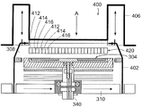
도 7a는 인클로저(402)를 기판 캐리어(304) 위로 이동시킴으로써 증착 챔버(400)가 형성되는 본 교시에 따른 증착 챔버(400)의 일 실시예의 측면도를 도시한다. 본 실시예에서, 기판 캐리어(304)는 수직 방향으로 고정된다. 예를 들어, 기판 캐리어(304)는, 트랙, 레일, 또는 컨베이어형 수송 시스템에 부착될 수 있고, 이러한 컨베이어형 수송 시스템은, 멀티 챔버 증착 시스템(100)(도 1)을 통해 수평 방향으로 (스핀들(340)에 의해 지지되는) 기판 캐리어(304)를 수송하는, 벨트, 푸시 로드, 자기 선형 모터 등의 자기 결합 드라이브도 포함할 수 있다. 액추에이터(406)는 기판 캐러어(304) 위로 수직 방향으로 인클로저(402)를 병진 운동시켜 증착 챔버(308)를 형성한다. 인클로저(402)는 수송 시스템(310)과 인터페이싱하여 증착 챔버(308) 내에 공정 화학 반응(process chemistry)을 함유하는 밀봉부를 형성한다. 일부 시스템에서, 수송 시스템(310)은 수송 시스템(310)의 상부에 또는 상면 내에 형성된 가스 밀봉부를 포함한다. 구체적인 일 실시예에서, 수송 시스템(310)은, O-링, 플랜지, 또는 가스켓을 압축하도록 인클로저(402)의 하부 에지가 O-링형 홈과 직접 접촉하는 상면 내에 형성된 O-링형 홈을 포함하는 컨베이어형 수송 시스템이며, 이에 따라 증착 챔버(308) 내에 공정 가스들을 상당히 함유하는 가스 밀봉부를 형성하게 된다.Figure 7A illustrates a side view of one embodiment of a
판(420)은 충분한 개수의 수평 장착 튜브들을 포함하며, 예를 들어, 기판 캐리어(308)의 상부로부터 적절한 거리에 위치할 수 있는 튜브들(412, 414, 416)(모든 튜브들이 식별된 것은 아님)을 포함한다. 챔버(308) 내의 구성에 따라, 튜브들(412, 414, 416)은, 챔버(308)에서 수행되는 MOCVD 공정에 따라, 각각 전구체 가스나 캐리어 가스를 반송할 수 있다. 많은 경우에, 불활성 가스를 반송하는 튜브는 캐리어 가스를 반송하는 튜브와 반응 가스를 반송하는 튜브 사이에 위치한다. 기판 캐리어(304)의 상면에 대면하는 튜브들의 하부에 위치하는 구멍이나 슬릿은 그 가스들이 캐리어(304)를 향하여 흐를 수 있게 한다.The
도 7b는 (많은 챔버 부품들이 제거되어 있는) 도 7a에 도시한 증착 챔버의 (도 7a에 도시한 바와 같이 A 방향으로의) 탑다운 도를 도시한다. 증착 챔버의 탑다운도는 튜브들(412, 414, 416)을 갖는 판(420)의 일 실시예를 예시한다. 튜브들(412, 414, 416)의 화살표들은 튜브 내의 가스 흐름의 일반적인 방향을 나타낸다. 당업자라면, 수행되는 구체적인 CVD 프로세스에 따라 가스들의 방향성 흐름이 변경될 수 있음을 인식할 것이다. 가스들은, 기판 캐리어(304)가 회전함에 따라 웨이퍼 상에 소망하는 에피택셜 구조가 성장되도록 적절한 유속으로 방출된다. 수평 모드에서 에피택셜 구조 성장의 균일성을 증가시키도록, 웨이퍼들은 일반적으로 행성 운동으로 자신의 축을 중심으로 회전해야 하며, 여기서 웨이퍼들이 장착되어 있는 웨이퍼 캐리어는, (웨이퍼 시트 내에서) 웨이퍼들을 웨이퍼 주위로 제2 속도로 회전시키는 동안 제1 속도로 회전하며, 이에 따라 웨이퍼 캐리어에서의 웨이퍼 들의 행성 운동을 생성한다. 이러한 시스템들은 행성 기어 시스템, 웨이퍼 캐리어를 회전시키는 모터 드라이버, 및 그 위에 배치된 웨이퍼를 이용하는 것으로 제안되어 왔다. 당업자라면, 소정의 상황에서 기판 캐리어(304)가 회전할 필요가 없음을 인식할 것이다.FIG. 7B shows a top down view (in the A direction as shown in FIG. 7A) of the deposition chamber shown in FIG. 7A (with many chamber parts removed). The top down view of the deposition chamber illustrates one embodiment of a
도 8은 본 교시에 따른 수평 흐름 가스 주입기 CVD 시스템(500)의 다른 변형예의 상측 사시도를 도시한다. 수평 흐름 가스 주입기(500)는, 판(420)과 튜브들(412, 414, 416)에 의해 제공되는 가스 흐름 대신에 또는 이러한 가스 흐름을 보충하도록 사용될 수 있다. CVD 시스템(500)은, 플래튼(510)의 평면에 전구체 가스들과 불활성 가스들(즉, 공정 챔버 내로의 수평 흐름)을 주입하는 원형 가스 주입기들(504, 506, 508)을 포함한다. 제1 원형 가스 주입기(504)는 제1 전구체 가스 소스(512)에 결합된다. 제2 원형 가스 주입기(506)는 불활성 가스 소스(514)에 결합된다. 제3 원형 가스 주입기(508)는 제2 전구체 가스 소스(516)에 결합된다. 일부 경우에는, 제1 및 제3 원형 가스 주입기들(504, 508)도 캐리어 가스 소스에 결합된다. 제1 원형 가스 주입기(504)는 제1 수평 영역(518)에 제1 전구체 가스를 주입한다. 제3 원형 가스 주입기(508)는 제2 수평 영역(520)에 제2 전구체 가스를 주입한다. 원형 전극(522)은, 제1 전구체 가스 분자들이 원형 전극(522)과 접하면서 또는 이러한 원형 전극에 근접하여 흐르도록 제1 수평 영역(518)에 위치한다. 원형 전극(522)을 제2 전구체 가스 분자들의 흐름으로부터 분리하도록 물리적 또는 화학적 배리어가 제1 및 제2 수평 영역들(518, 520) 사이에 위치할 수 있다.FIG. 8 shows a top perspective view of another variant of a horizontal flow gas
일부 경우에, 배플은, 제1 전구체 가스 분자들이 플래튼(510)으로 흐를 때 전극(522)에 의해 열적으로 활성화되는 것을 실질적으로 방지하도록 원형 전극(522) 위에 위치한다. 일부 경우에는, 가스 커튼을 사용하여 제1 및 제2 수평 영역들(518, 520)을 분리한다. 이러한 시스템들에서, 제2 원형 가스 주입기(506)는, 제2 전구체 가스 분자들이 원형 전극(522)에 의해 활성화되는 것을 실질적으로 방지하는 패턴으로 제1 및 제2 수평 영역들(518, 520) 사이에 불활성 가스를 주입한다.In some cases, the baffle is located above the
CVD 시스템(500)을 작동시키는 방법은, 제1 원형 가스 주입기(504)로 제1 전구체 가스를 주입하는 단계와 제3 원형 가스 주입기(508)로 제2 전구체 가스를 주입하는 단계를 포함한다. 불활성 가스는, 제2 원형 가스 주입기(506)에 의해 제1 및 제2 수평 영역들(518, 520) 사이에 주입되어, 제2 전구체 가스 분자들이 원형 전극(522)에 의해 활성화되는 것을 방지하는 화학적 배리어를 형성하게 된다. 전원(220)에 의해 원형 전극(522)이 전력을 공급받으면, 원형 전극(522)은, 제1 원형 가스 주입기(504)에 의해 주입되어 원형 전극(522)과 접촉하면서 흐르거나 이러한 원형 전극에 근접하여 흐르는 제1 전구체 가스 분자들을 열적으로 활성화시킨다. 이어서, 활성화된 제1 전구체 가스 분자들과 제2 전구체 가스 분자들은 기판들(524)의 표면 위로 흐르고, 이에 따라 반응하여 에피택셜층을 형성한다. 필요시 (예를 들어, 인클로저에 인접하여 또는 캐리어 아래에) 퍼지 가스들도 추가하여 이러한 영역들에 기생 증착이 없게 할 수 있다. 기생 증착으로 인해, 메모리 효과, 미립자 오염, 흐름 차단, 및 유해 축적이 발생할 수 있고, 이들 모두는 CVD 의 바람직하지 못한 부작용들이다.The method of operating the
도 9는 본 교시에 따른 수평 흐름 가스 주입기 CYD 시스템의 또 다른 변형예의 측면도를 도시한다. 기판 캐리어(182)는 서셉터(186)와 기판 캐리어 조립체(184)를 포함한다. 서셉터(186)와 기판 캐리어 조림체(184)를 포함하는 기판 캐리어(182)는, 전술한 바와 같이 행성형 캐리어이고, 통상적으로, 열 에너지가 가열기(192)로부터 기판으로 쉽게 전도되도록 고온에서 고 열 전도성을 갖는 재료로 되어 있다. 전술한 바와 같이, 스핀들(140)은 서셉터(186)를 지지하고, 스핀들(140)은 수송 기구(104)에 연결된다. 챔버(198)는, 기판 캐리어(184)를, 멀티존 샤워헤드(multi-zone showerhead; 188)에 의해 정의되는 비이동식 정면, 후면, 및 측벽들과 천정으로부터 형성되는 인클로저(190) 내로 이동시킴으로써 형성된다. 인클로저(190) 등의 인클로저들은 조립 영역 내의 다양한 위치에 위치할 수 있고, 수직 및 수평을 이루도록 수직 방향과 수평 방향으로 고정된다.Figure 9 shows a side view of another variant of the horizontal flow gas injector CYD system according to the present teachings. The
인클로저(190)는 형성된 위치에 있는 것으로 도시되어 있다. 도 2b에 도시한 실시예와 유사하게, 액추에이터(104)는, 기판 캐리어(182)가 인클로저(190) 아래에 적절히 정렬될 때까지 기판 캐리어(182)를 수평 방향으로 병진 운동시킨다. 이어서, 액추에이터(도시하지 않음)는 기판 캐리어(182)를 수직 방향으로 인클로저(190) 내로 이동시켜 증착 챔버(198)를 형성한다. 이 시스템은 또한 도 2b에 관하여 전술한 바와 같이 추가 방식으로 이동될 수도 있다. 적절한 밀봉부를 배치하여 공정 가스들의 누출을 방지한다.
이 시스템의 일부로서, 공정 가스들의 서로 다른 2개의 구성이 도시되어 있으며, 당업자라면, 공정 가스들을 챔버(198) 내에 수평으로 도입하기 위한 다른 많은 구성이 존재함을 인식할 것이다. 공정 가스들은, 주입기(222)에서 3개의 가스(A, B, C)를 함유하는 구성(194)으로부터 챔버에 유입될 수 있다. 배기부(180)는 챔버(198) 위의 중심에 위치하고, 가스 상 핵생성을 방지하거나 감소시키고 챔버 내의 가스 흐름 정체를 피하도록 가열된다. 공정 가스들은, 또한, 주입기(224)에서 3개의 가스(D, E, F)를 함유하는 구성(196)으로부터 챔버에 유입될 수 있다. 주입기들(222 또는 224)은, 공정 가스들의 제어식 예비 혼합, 암모니아와 기타 불활성 가스들의 예열을 제공할 수 있고 챔버 벽들로부터 챔버의 중심으로 가스들의 방사상 흐름을 제공할 수 있는 3개 존 주변형(three zone peripheral type) 주입기들이다.As part of this system, two different configurations of process gases are shown, and those skilled in the art will recognize that there are many other configurations for introducing process gases into the
일부 시스템들에서는, 캐리어 표면에 대략 수직인 방향으로 하나의 전구체 또는 캐리어 가스를 주입하고 캐리어 표면에 대략 평행한 방향으로 다른 하나의 전구체 또는 캐리어 가스를 주입하는 것이 유리할 수 있다.In some systems it may be advantageous to inject one precursor or carrier gas in a direction generally perpendicular to the carrier surface and another precursor or carrier gas in a direction approximately parallel to the carrier surface.
본 교시의 멀티 챔버 증착 시스템의 한 가지 특징은, 이 시스템이 매우 높은 처리량을 가질 수 있고, 따라서 대량 생산 예에 특히 적합하다는 점이다. 높은 처리량은, 복수의 증착 챔버의 각각이 특정한 층 구조를 특정한 두께로 성장시키도록 최적화될 수 있기 때문에, 얻어질 수 있다. 증착 챔버들(110, 152) 내에 또는 이러한 증착 챔버들에 근접하여 가열기들(122A, 122B)이 고정된 실시예들에서, 가열기들(122A, 122B)은, 기판들의 성장 표면들을 해당 소망 온도로 가열하는 좁은 온도 범위에서 작동될 수 있다. 이러한 시스템들에서는, 성장 표면들이 해당 소망 성장 온도에 도달하는 데 걸리는 시간을 최소화할 수 있다.One feature of the multi-chamber deposition system of the present teachings is that the system can have a very high throughput and is therefore particularly suitable for mass production examples. The high throughput can be obtained since each of the plurality of deposition chambers can be optimized to grow a particular layer structure to a specific thickness. In the embodiments in which the
본 교시의 멀티 챔버 증착 시스템의 다른 한 가지 특징은, 이 시스템이 서로 다른 재료 층 구조들을 증착하도록 쉽게 재구성되며 또한 연구 및 시험 환경에 매우 적합하다는 점이다. 본 교시의 멀티 챔버 증착 시스템의 또 다른 한 가지 특징은, 기판들의 각각이 대략 동일한 공정 조건들에 노출되기 때문에 이 시스템이 상당히 반복가능하다는 점이다. 각 챔버에 공정 단계들의 서브세트가 할당되므로, 각 챔버에 대한 진성 공정 안정성(intrinsic process stability)이 개선된다. 이전 단계로부터의 잔여 가스 오염에 민감한 이질적인 공정 단계들이 동일한 챔버에서 수행될 때 발생할 수 있는 누화 및 메모리 효과를, 본 교시의 인라인 아키텍처(in-line architecture)에서 본질적으로 피할 수 있다.Another feature of the multi-chamber deposition system of the present teachings is that the system is easily reconfigured to deposit different material layer structures and is also well suited for research and test environments. Another feature of the multi-chamber deposition system of the present teachings is that the system is significantly repeatable because each of the substrates is exposed to approximately the same process conditions. Since each chamber is assigned a subset of the process steps, the intrinsic process stability for each chamber is improved. Crosstalk and memory effects that can occur when heterogeneous process steps sensitive to residual gas contamination from previous steps are performed in the same chamber can be essentially avoided in the in-line architecture of the present teachings.
본 교시의 멀티 챔버 증착 시스템의 다른 한 가지 특징은, 이 시스템이 복수의 증착 챔버(110, 152) 내의 기판들 상에 증착되는 층들의 현장내 특징화를 수행하도록 쉽게 구성될 수 있다는 점이다. 당업자라면, 현장내 측정 디바이스의 다양한 유형들을 이용하여 복수의 증착 챔버(110) 내에서 또는 복수의 증착 챔버(110, 152) 사이에서 증착된 막들을 특징화할 수 있음을 인식할 것이다. 측정은, 또한, 현장내 측정 디바이스들을 포함하는 짧은 섹션을 포함함으로써 기판들이 다수의 챔버들에 걸쳐 이동하고 있을 때 수행될 수도 있다.Another feature of the multi-chamber deposition system of the present teachings is that this system can be easily configured to perform in-situ characterization of the layers deposited on the substrates in the plurality of
일반적으로, 본 교시에 따른 멀티 챔버 화학적 기상 증착 시스템을 이용하여 기판 상에 다수의 에피택셜층들을 형성하는 방법은, 제1 위치에서 적어도 하나의 기판을 포함하는 제1 회전가능 기판 캐리어를 밀폐하여 제1 독립적 환경을 유지하는 제1 증착 챔버를 형성하는 단계를 포함하고, 이 환경은 화학적 기상 증착 공정 화학 반응 환경(chemical vapor deposition process chemistry environment)이다. 제1 기판 캐리어를 밀폐하여 제1 증착 챔버를 형성하는 단계는, 제1 기판 캐리어 위로 인클로저를 이동시켜 제1 증착 챔버 내의 제1 화학적 기상 증착 공정 화학 반응(the first chemical vapor deposition process chemistry)을 분리하는 단계를 포함한다. 제1 기판 캐리어를 밀폐하여 제1 증착 챔버를 형성하는 단계는, 또한, 제1 기판 캐리어를 인클로저 또는 챔버 내로 이동시켜 제1 증착 챔버 내의 제1 화학적 기상 증착 공정 화학 반응을 분리하는 단계를 포함할 수 있다. 대안으로, 제1 기판 캐리어를 밀폐하여 제1 증착 챔버를 형성하는 단계는, 가스 커튼을 형성하여 제1 화학적 기상 증착 공정 화학 반응을 분리하는 단계를 포함할 수 있다.Generally, a method of forming a plurality of epitaxial layers on a substrate using a multi-chamber chemical vapor deposition system according to the present teachings comprises sealing a first rotatable substrate carrier comprising at least one substrate in a first position Forming a first deposition chamber that maintains a first independent environment, the environment being a chemical vapor deposition process chemistry environment. The step of sealing the first substrate carrier to form the first deposition chamber comprises moving the enclosure over the first substrate carrier to isolate the first chemical vapor deposition process chemistry in the first deposition chamber . The step of sealing the first substrate carrier to form the first deposition chamber also includes separating the first chemical vapor deposition process chemical reaction in the first deposition chamber by moving the first substrate carrier into the enclosure or chamber . Alternatively, the step of sealing the first substrate carrier to form the first deposition chamber may include forming a gas curtain to separate the first chemical vapor deposition process chemistry.
제1 에피택셜층은, 제1 독립적 화학적 기상 증착 공정 화학 반응(the first independent chemical vapor deposition process chemistry)에 의해 제1 위치에서 제1 증착 챔버의 적어도 하나의 기판 상에서 성장된다. 적어도 하나의 기판 상에 제1 에피택셜층을 성장시키기 위한 임의의 수단을 이용할 수 있다. 제1 증착 챔버의 내부 또는 외부에 위치하는 가열기를 이용하여 적어도 하나의 기판의 성장 표면을 가열한다. 화학적 기상 증착에 의해 소망하는 막이 증착되게 하는 유속으로 제1 증착 챔버에 적어도 하나의 CVD 공정 가스를 제공한다. 적어도 하나의 CVD 공정 가스는 적어도 하나의 MOCVD 가스일 수 있다.The first epitaxial layer is grown on at least one substrate of the first deposition chamber at a first location by a first independent chemical vapor deposition process chemistry. Any means for growing the first epitaxial layer on at least one substrate may be used. A heater is located inside or outside the first deposition chamber to heat the growth surface of the at least one substrate. Provides at least one CVD process gas to the first deposition chamber at a flow rate that causes the desired film to be deposited by chemical vapor deposition. The at least one CVD process gas may be at least one MOCVD gas.
제1 기판 캐리어는, 제1 에피택셜층이 제2 위치로 성장된 후에 수송된다. 일부 방법에서는, 제1 기판 캐리어에 연관된 가열기가 제1 기판 캐리어와 함께 수송된다. 제1 기판 캐리어는, 벨트, 푸시 로드, 및 자기 선형 모터 등의 자기적 결합 드라이브도 포함할 수 있는 컨베이어형 기구, 트랙, 또는, 레일을 따르는 트랜스포테이션 등의 많은 수단에 의해 수송될 수 있다. 이어서, 제1 기판 캐리어를 밀폐하여, 제2 독립적 화학적 기상 증착 공정 화학 반응(a second independent chemical vapor deposition process chemistry)을 유지하는 제2 증착 챔버를 형성한다.The first substrate carrier is transported after the first epitaxial layer has grown to the second location. In some methods, a heater associated with the first substrate carrier is transported with the first substrate carrier. The first substrate carrier may be transported by any number of means, such as a conveyor-type device, a track, or a transport along a rail, which may also include a magnetically coupled drive, such as a belt, pushrod, and magnetic linear motor . The first substrate carrier is then sealed to form a second deposition chamber that maintains a second independent chemical vapor deposition process chemistry.
제2 에피택셜층은, 제2 독립적 화학적 기상 증착 공정 화학 반응에 의해 제2 위치에서 제2 증착 챔버의 제1 에피택셜층 상부에 성장된다. 적어도 하나의 기판 상에 제2 에피택셜층을 성장시키기 위한 임의의 수단을 이용할 수 있다. 제2 증착 챔버의 내부 또는 외부에 위치하는 가열기를 이용하여 적어도 하나의 기판의 성장 표면과 CVD 공정 가스들을 가열한다.A second epitaxial layer is grown on the first epitaxial layer of the second deposition chamber at a second location by a second independent chemical vapor deposition process chemistry. Any means for growing a second epitaxial layer on at least one substrate may be used. A heater located inside or outside the second deposition chamber is used to heat the growth surface of the at least one substrate and the CVD process gases.
또한, 각 수송 시퀀스 내에서, 즉, (기판들이 로딩되어 있는) 기판 캐리어가 하나의 챔버로부터 다른 하나의 챔버로 이동되기 전에 각 챔버 내에서 다수의 에피텍셜층들 또는 층들의 스택을 증착할 수도 있다.It is also possible to deposit a plurality of epitaxial layers or stacks of layers within each chamber within each transport sequence, i. E., Before the substrate carrier (on which the substrates are loaded) is moved from one chamber to the other have.
적어도 하나의 CVD 공정 가스를, 소망하는 막이 화학적 기상 증착에 의해 증착되게 하는 유속으로 제2 증착 챔버에 제공한다. 이 적어도 하나의 CVD 공정 가스는 적어도 하나의 MOCVD 가스일 수 있다. 방법은, 소망하는 CVD 가스들을 제1 및 제2 증착 챔버들의 각각에 제공하도록 가스 분배 매니폴드를 구성하는 단계를 포함할 수 있다.At least one CVD process gas is provided to the second deposition chamber at a flow rate such that the desired film is deposited by chemical vapor deposition. The at least one CVD process gas may be at least one MOCVD gas. The method may include configuring a gas distribution manifold to provide desired CVD gases to each of the first and second deposition chambers.
멀티 챔버 화학적 기상 증착 시스템을 이용하여 기판 상에 다수의 에피택셜층들을 형성하는 방법은 제2 회전가능 기판 캐리어로 계속된다. 제1 위치에서 적어도 하나의 기판을 포함하는 제2 회전가능 기판 캐리어는, 제1 독립적 화학적 기상 증착 공정 화학 반응을 유지하는 제1 증착 챔버를 형성하도록 밀폐된다. 이어서, 제1 에피택셜층은, 제1 독립적 화학적 기상 증착 공정 화학 반응에 의해 제1 위치에서 제1 증착 챔버의 제2 기판 캐리어 상에 위치하는 기판들 상에서 성장된다. 제1 및 제2 기판 캐리어들 상의 적어도 하나의 기판은 통상적으로 제 시간에 동시 처리된다.A method of forming a plurality of epitaxial layers on a substrate using a multi-chamber chemical vapor deposition system continues with a second rotatable substrate carrier. A second rotatable substrate carrier comprising at least one substrate in a first position is sealed to form a first deposition chamber that maintains a first independent chemical vapor deposition process chemistry. The first epitaxial layer is then grown on the substrates positioned on the second substrate carrier of the first deposition chamber at a first location by a first independent chemical vapor deposition process chemistry. At least one substrate on the first and second substrate carriers is typically co-processed in time.
방법은, 제2 에피택셜층이 제3 위치로 성장된 후 수송되고 있는 제1 기판 캐리어로 계속된다. 이어서, 적어도 하나의 기판을 포함하는 제1 회전가능 기판 캐리어를 제3 위치에서 밀폐하여, 제3 독립적 화학적 기상 증착 공정 화학 반응(a third independent chemical vapor deposition process chemistry)을 유지하는 제3 증착 챔버를 형성한다. 일부 방법에서는, 제3 기판 캐리어에 연관된 가열기를 제3 기판 캐리어와 함께 수송한다. 제2 회전가능 기판 캐리어를, 제2 회전가능 기판 캐리어가 밀폐되어 제2 독립적 화학적 기상 증착 공정 화학 반응을 유지하는 제2 증착 챔버가 형성되는 제2 위치로 수송한다. 제3 회전가능 기판 캐리어를, 제3 회전가능 기판 캐리어가 밀폐되어 제1 독립적 화학적 기상 증착 공정 화학 반응을 유지하는 제1 증착 챔버가 형성되는 제1 위치로 수송한다. 제1, 제2, 및 제3 기판 캐리어들의 수송은 동시에 수행될 수 있다. 또한, 증착은 제1, 제2, 및 제3 증착 챔버들에서 동시에 수행될 수 있다. 이 방법은 제4 기판 캐리어 및 추가 기판 캐리어에 대하여 계속된다. 전술한 바와 같이, 모든 챔버들이 CVD 공정들에 대하여 유사하지 않을 수도 있고 또는 사용되지 않을 수도 있다. 일부 챔버들은, 캐리어의 베이킹/가열, 공정 단계 전의 또는 공정 단계 후의 어닐링, 공정 단계 전의 또는 공정 단계 후의 공정 시퀀스(process sequence)나 표면 개질 단계(surface modification step)의 종료시 냉각에만 배타적으로 해당될 수 있다.The method continues with the first substrate carrier being transported after the second epitaxial layer has been grown to the third location. A first rotatable substrate carrier comprising at least one substrate is then sealed in a third position to form a third deposition chamber that maintains a third independent chemical vapor deposition process chemistry . In some methods, the heater associated with the third substrate carrier is transported with the third substrate carrier. The second rotatable substrate carrier is transported to a second position where the second rotatable substrate carrier is sealed to form a second deposition chamber that maintains a second independent chemical vapor deposition process chemistry. The third rotatable substrate carrier is transported to a first position where the third rotatable substrate carrier is sealed to form a first deposition chamber that maintains a first independent chemical vapor deposition process chemistry. Transport of the first, second, and third substrate carriers may be performed simultaneously. Further, the deposition can be performed simultaneously in the first, second, and third deposition chambers. The method continues for a fourth substrate carrier and an additional substrate carrier. As described above, not all chambers may or may not be similar to CVD processes. Some chambers may exclusively be cooled exclusively during baking / heating of the carrier, annealing before or after the process step, cooling at the end of the process sequence or surface modification step before or after the process step have.
본 교시에 따른 다른 방법과 시스템에서, 기판 캐리어는 회전가능한 캐리어가 아니다. 당업자라면, 전술한 본 교시에 따른 방법들에 의해 또는 이러한 시스템에서 에피택셜층들을 어떻게 증착하고 성장시킬지를 인식할 것이다.In other methods and systems in accordance with the present teachings, the substrate carrier is not a rotatable carrier. One of ordinary skill in the art will recognize how to deposit and grow epitaxial layers in the system or in the system according to the above teachings.
본 교시에 따른 일부 방법들에 있어서, 증착된 재료 층 특성들의 현장내 측정은 증착 동안 수행된다. 예를 들어, 제1 및 제2 에피택셜층들 중 하나 이상을 성장시키는 동안 현장내 고온 측정을 수행하여 기판 표면에서의 성장 온도를 감시할 수 있다. 또한, 증착된 막들의 막 두께 및/또는 성장 속도를 측정하도록 현장내 반사율계를 미리 형성할 수 있다.In some methods according to the present teachings, in situ measurements of deposited material layer properties are performed during deposition. For example, in situ high temperature measurements may be performed during growth of one or more of the first and second epitaxial layers to monitor the growth temperature at the substrate surface. An in situ reflectance meter may also be preformed to measure the film thickness and / or growth rate of the deposited films.
균등물Equalization
다양한 실시예들로 출원인의 교시를 설명하였지만, 출원인의 교시를 이러한 실시예들로 한정하려는 것은 아니다. 오히려, 당업자라면 인식하듯이, 출원인의 교시는 다양한 대체예, 수정예, 균등물을 포함하며, 이는 본 교시의 사상과 범위를 벗어나지 않고서 행해질 수 있다.While the teachings of the applicant have been described in various embodiments, it is not intended to limit the applicant's teachings to such embodiments. Rather, those skilled in the art will recognize that the teachings of the applicants include various alternatives, modifications, and equivalents, which can be made without departing from the spirit and scope of the present teachings.
Claims (70)
a. 각 기판 캐리어마다 하나 이상의 기판을 지지하도록 구성된 복수의 기판 캐리어와,
b. 각 복수의 인클로저마다 상기 복수의 기판 캐리어 중 하나를 밀폐하여 처리 단계를 수행하기 위한 독립적 환경을 유지하는 증착 챔버를 형성하도록 구성된 복수의 인클로저(enclosure)와,
c. 상기 복수의 기판 캐리어의 각각을, 미리 정해진 시간 동안 상기 복수의 인클로저에서 처리 단계들이 수행될 수 있게 하는 이산적 스텝(discrete steps)으로 상기 복수의 인클로저의 각각으로 수송하는 수송 기구를 포함하는, 멀티 챔버 CVD 처리 시스템.A multi-chamber CVD processing system comprising:
a. A plurality of substrate carriers configured to support at least one substrate for each substrate carrier,
b. A plurality of enclosures configured to seal a respective one of the plurality of substrate carriers for each of the plurality of enclosures to form a deposition chamber that maintains an independent environment for performing processing steps;
c. And a transport mechanism for transporting each of the plurality of substrate carriers to each of the plurality of enclosures in discrete steps that allow processing steps in the plurality of enclosures to be performed for a predetermined period of time. Chamber CVD processing system.
a. 각 기판 캐리어마다 하나 이상의 기판을 지지하도록 구성된 복수의 기판 캐리어와,
b. 각 복수의 인클로저마다 상기 복수의 기판 캐리어 중 하나를 밀폐하여 처리 단계를 수행하기 위한 독립적 환경을 유지하는 증착 챔버를 형성하도록 구성된 복수의 인클로저와,
c. 각 가열기마다 상기 복수의 기판 중 대응하는 하나를 상기 처리 단계를 수행하기 위한 소망하는 공정 온도로 가열하는 복수의 가열기와,
d. 상기 복수의 기판 캐리어의 각각을, 미리 정해진 시간 동안 상기 복수의 인클로저에서 처리 단계들이 수행될 수 있게 하는 이산적 스텝으로 상기 복수의 인클로저의 각각으로 수송하는 수송 기구를 포함하는, 멀티 챔버 CVD 공정 시스템.As a multi-chamber CVD process system,
a. A plurality of substrate carriers configured to support at least one substrate for each substrate carrier,
b. A plurality of enclosures configured to seal the one of the plurality of substrate carriers for each of the plurality of enclosures to form a deposition chamber that maintains an independent environment for performing the processing steps,
c. A plurality of heaters for heating each corresponding one of the plurality of substrates to a desired processing temperature for performing the processing step for each heater,
d. And a transport mechanism that transports each of the plurality of substrate carriers to each of the plurality of enclosures in a discrete step that allows processing steps in the plurality of enclosures to be performed for a predetermined period of time. .
a. 제1 위치에서 하나 이상의 기판을 포함하는 제1 기판 캐리어를 밀폐하여 제1 독립적 환경을 유지하는 제1 증착 챔버를 형성하는 단계와,
b. 상기 제1 독립적 환경이 있는 상기 제1 위치에서 상기 제1 증착 챔버 내의 상기 하나 이상의 기판 상에 제1 에피택셜층을 성장시키는 단계와,
c. 상기 제1 에피택셜층이 성장된 후 상기 제1 기판 캐리어를 제2 위치로 수송하고, 상기 제1 기판 캐리어를 밀폐하여 제2 독립적 환경을 유지하는 제2 증착 챔버를 형성하는 단계와,
d. 상기 제2 독립적 환경이 있는 상기 제2 위치에서 상기 제2 증착 챔버 내에 상기 제1 에피택셜층 상에 제2 에피택셜층을 성장시키는 단계를 포함하는, 에피택셜층 형성 방법.A method of forming a plurality of epitaxial layers on a substrate using a multi-chamber chemical vapor deposition system,
a. Sealing a first substrate carrier comprising at least one substrate at a first location to form a first deposition chamber maintaining a first independent environment,
b. Growing a first epitaxial layer on the at least one substrate in the first deposition chamber at the first location having the first independent environment,
c. Transporting the first substrate carrier to a second location after the first epitaxial layer is grown and sealing the first substrate carrier to form a second deposition chamber maintaining a second independent environment;
d. And growing a second epitaxial layer on the first epitaxial layer in the second deposition chamber at the second location having the second independent environment.
a. 상기 제1 위치에서 하나 이상의 기판을 포함하는 제2 기판 캐리어를 밀폐하여 상기 제1 독립적 환경을 유지하는 상기 제1 증착 챔버를 형성하는 단계와,
b. 상기 제1 독립적 환경이 있는 상기 제1 위치에서 상기 제1 증착 챔버 내에 상기 제2 기판 캐리어의 상기 하나 이상의 기판 상에 상기 제1 에피택셜층을 성장시키는 단계를 더 포함하는, 에피택셜층 형성 방법.49. The method of claim 48,
a. Sealing the second substrate carrier comprising the one or more substrates at the first location to form the first deposition chamber maintaining the first independent environment,
b. Further comprising growing the first epitaxial layer on the at least one substrate of the second substrate carrier in the first deposition chamber at the first location having the first independent environment .
a. 복수의 고정 위치에서 하나 이상의 기판을 지지하는 복수의 기판 캐리어를 밀폐하여 독립적 환경을 각각 유지하는 복수의 증착 챔버를 형성하기 위한 수단과,
b. 상기 독립적 환경을 각각 유지하고 있는 상기 복수의 증착 챔버 내의 상기 복수의 기판 캐리어에 의해 지지되는 상기 하나 이상의 기판 상에 에피택셜층을 성장시키기 위한 수단과,
c. 상기 복수의 증착 챔버 간에 상기 복수의 기판 캐리어를 이산적 스텝으로 수송하기 위한 수단을 포함하는, 멀티 챔버 화학적 기상 증착 시스템.A multi-chamber chemical vapor deposition system comprising:
a. Means for forming a plurality of deposition chambers each holding an independent environment by sealing a plurality of substrate carriers supporting at least one substrate at a plurality of fixed positions,
b. Means for growing an epitaxial layer on said at least one substrate supported by said plurality of substrate carriers in said plurality of deposition chambers each maintaining said independent environment;
c. And means for transporting the plurality of substrate carriers between the plurality of deposition chambers in discrete steps.
Applications Claiming Priority (3)
| Application Number | Priority Date | Filing Date | Title |
|---|---|---|---|
| US13/185,450 | 2011-07-18 | ||
| US13/185,450 US20110290175A1 (en) | 2009-06-07 | 2011-07-18 | Multi-Chamber CVD Processing System |
| PCT/US2012/045179 WO2013012549A2 (en) | 2011-07-18 | 2012-07-02 | Multi-chamber cvd processing system |
Publications (1)
| Publication Number | Publication Date |
|---|---|
| KR20140051232A true KR20140051232A (en) | 2014-04-30 |
Family
ID=47558660
Family Applications (1)
| Application Number | Title | Priority Date | Filing Date |
|---|---|---|---|
| KR1020147000821A KR20140051232A (en) | 2011-07-18 | 2012-07-02 | Multi-chamber cvd processing system |
Country Status (7)
| Country | Link |
|---|---|
| US (1) | US20110290175A1 (en) |
| EP (1) | EP2735020A4 (en) |
| JP (1) | JP2014524151A (en) |
| KR (1) | KR20140051232A (en) |
| CN (1) | CN103703544A (en) |
| TW (1) | TW201309841A (en) |
| WO (1) | WO2013012549A2 (en) |
Families Citing this family (39)
| Publication number | Priority date | Publication date | Assignee | Title |
|---|---|---|---|---|
| EP2215282B1 (en) | 2007-10-11 | 2016-11-30 | Valence Process Equipment, Inc. | Chemical vapor deposition reactor |
| JP5088335B2 (en) * | 2009-02-04 | 2012-12-05 | 東京エレクトロン株式会社 | Substrate transfer apparatus and substrate processing system |
| US10689753B1 (en) * | 2009-04-21 | 2020-06-23 | Goodrich Corporation | System having a cooling element for densifying a substrate |
| US8354618B1 (en) * | 2010-06-30 | 2013-01-15 | Wd Media, Inc. | Load chamber with dual heaters |
| WO2012142408A2 (en) * | 2011-04-14 | 2012-10-18 | Veeco Instruments Inc. | Substrate holders and methods of substrate mounting |
| US8807318B2 (en) * | 2011-09-20 | 2014-08-19 | International Business Machines Corporation | Multi-generational carrier platform |
| US20130171350A1 (en) * | 2011-12-29 | 2013-07-04 | Intermolecular Inc. | High Throughput Processing Using Metal Organic Chemical Vapor Deposition |
| US20130192761A1 (en) * | 2012-01-31 | 2013-08-01 | Joseph Yudovsky | Rotary Substrate Processing System |
| US9478797B2 (en) * | 2013-01-25 | 2016-10-25 | Applejack 199 L.P. | System, method and apparatus for forming a thin film lithium ion battery |
| TWI683382B (en) * | 2013-03-15 | 2020-01-21 | 應用材料股份有限公司 | Carousel gas distribution assembly with optical measurements |
| US9093599B2 (en) * | 2013-07-26 | 2015-07-28 | First Solar, Inc. | Vapor deposition apparatus for continuous deposition of multiple thin film layers on a substrate |
| TWI650832B (en) * | 2013-12-26 | 2019-02-11 | 維克儀器公司 | Wafer carrier having thermal cover for chemical vapor deposition systems |
| CN104976297B (en) * | 2014-04-14 | 2017-12-05 | 睿励科学仪器(上海)有限公司 | The mechanical driving device of full automatic standard ellipsometer |
| CN103898475B (en) * | 2014-04-21 | 2017-01-18 | 清远先导材料有限公司 | Multi-chamber graphite deposition device and chemical vapor deposition furnace |
| JP6285305B2 (en) * | 2014-07-22 | 2018-02-28 | 住友化学株式会社 | Semiconductor manufacturing apparatus and semiconductor manufacturing method |
| US9390910B2 (en) * | 2014-10-03 | 2016-07-12 | Applied Materials, Inc. | Gas flow profile modulated control of overlay in plasma CVD films |
| US10954597B2 (en) * | 2015-03-17 | 2021-03-23 | Asm Ip Holding B.V. | Atomic layer deposition apparatus |
| JP2016219568A (en) * | 2015-05-19 | 2016-12-22 | 株式会社ニューフレアテクノロジー | Vapor growth apparatus and vapor growth method |
| CN105039931A (en) * | 2015-08-31 | 2015-11-11 | 清远先导材料有限公司 | Chemical vapor deposition furnace and chemical vapor deposition system |
| US10550469B2 (en) * | 2015-09-04 | 2020-02-04 | Lam Research Corporation | Plasma excitation for spatial atomic layer deposition (ALD) reactors |
| TWI729101B (en) | 2016-04-02 | 2021-06-01 | 美商應用材料股份有限公司 | Apparatus and methods for wafer rotation in carousel susceptor |
| TWI734770B (en) | 2016-04-24 | 2021-08-01 | 美商應用材料股份有限公司 | Apparatus for prevention of backside deposition in a spatial ald process chamber |
| US11015246B2 (en) | 2016-04-24 | 2021-05-25 | Applied Materials, Inc. | Apparatus and methods for depositing ALD films with enhanced chemical exchange |
| US11339478B2 (en) * | 2016-09-19 | 2022-05-24 | King Abdullah University Of Science And Technology | Susceptor |
| US10167558B1 (en) | 2017-10-13 | 2019-01-01 | International Business Machines Corporation | Phase shifted gas delivery for high throughput and cost effectiveness associated with atomic layer etching and atomic layer deposition |
| TWI802439B (en) | 2017-10-27 | 2023-05-11 | 美商應用材料股份有限公司 | Single wafer processing environments with spatial separation |
| USD860146S1 (en) | 2017-11-30 | 2019-09-17 | Veeco Instruments Inc. | Wafer carrier with a 33-pocket configuration |
| WO2019182260A1 (en) * | 2018-03-23 | 2019-09-26 | 홍잉 | Inline thin film processing device |
| USD863239S1 (en) | 2018-03-26 | 2019-10-15 | Veeco Instruments Inc. | Chemical vapor deposition wafer carrier with thermal cover |
| USD866491S1 (en) | 2018-03-26 | 2019-11-12 | Veeco Instruments Inc. | Chemical vapor deposition wafer carrier with thermal cover |
| USD854506S1 (en) | 2018-03-26 | 2019-07-23 | Veeco Instruments Inc. | Chemical vapor deposition wafer carrier with thermal cover |
| USD860147S1 (en) | 2018-03-26 | 2019-09-17 | Veeco Instruments Inc. | Chemical vapor deposition wafer carrier with thermal cover |
| USD858469S1 (en) | 2018-03-26 | 2019-09-03 | Veeco Instruments Inc. | Chemical vapor deposition wafer carrier with thermal cover |
| EA034967B1 (en) * | 2018-05-04 | 2020-04-13 | Общество С Ограниченной Ответственностью "Изовак Технологии" | Process line for vacuum formation of thin-film coatings (embodiments) |
| TWI754179B (en) * | 2018-10-29 | 2022-02-01 | 美商應用材料股份有限公司 | Spatial wafer processing with improved temperature uniformity |
| KR102264556B1 (en) * | 2019-07-18 | 2021-06-11 | 시너스텍 주식회사 | Atomic layer deposition apparatus |
| WO2021016493A1 (en) * | 2019-07-23 | 2021-01-28 | The Regents Of The University Of Michigan | Integrated electrohydrodynamic jet printing and spatial atomic layer deposition system for area-selective atomic layer deposition |
| WO2022123083A2 (en) * | 2020-12-11 | 2022-06-16 | Zadient Technologies SAS | Method and device for producing a sic solid material |
| CN117265650A (en) * | 2023-09-20 | 2023-12-22 | 江苏汉印机电科技股份有限公司 | Silicon carbide epitaxial chemical vapor deposition system |
Family Cites Families (10)
| Publication number | Priority date | Publication date | Assignee | Title |
|---|---|---|---|---|
| US6063248A (en) * | 1998-11-12 | 2000-05-16 | Hmt Technology Corporation | Process chamber isolation system in a deposition apparatus |
| US6349270B1 (en) * | 1999-05-27 | 2002-02-19 | Emcore Corporation | Method and apparatus for measuring the temperature of objects on a fast moving holder |
| US6631726B1 (en) * | 1999-08-05 | 2003-10-14 | Hitachi Electronics Engineering Co., Ltd. | Apparatus and method for processing a substrate |
| US6576062B2 (en) * | 2000-01-06 | 2003-06-10 | Tokyo Electron Limited | Film forming apparatus and film forming method |
| US20030079369A1 (en) * | 2001-10-29 | 2003-05-01 | Power Paper Ltd. | Process and apparatus for drying drying a thick film layer |
| US20040065255A1 (en) * | 2002-10-02 | 2004-04-08 | Applied Materials, Inc. | Cyclical layer deposition system |
| US20050115492A1 (en) * | 2003-11-28 | 2005-06-02 | Chia-Cheng Liu | Method and apparatus of the chemical metal organic vapor epitaxy for the multi-chamber epitaxy layer deposition |
| US7438175B2 (en) * | 2005-06-10 | 2008-10-21 | Applied Materials, Inc. | Linear vacuum deposition system |
| US20100310769A1 (en) * | 2009-06-07 | 2010-12-09 | Veeco Compound Semiconductor, Inc. | Continuous Feed Chemical Vapor Deposition System |
| WO2011031672A2 (en) * | 2009-09-09 | 2011-03-17 | Applied Materials, Inc. | Parallel system for epitaxial chemical vapor deposition |
-
2011
- 2011-07-18 US US13/185,450 patent/US20110290175A1/en not_active Abandoned
-
2012
- 2012-07-02 CN CN201280035420.2A patent/CN103703544A/en active Pending
- 2012-07-02 JP JP2014521643A patent/JP2014524151A/en active Pending
- 2012-07-02 WO PCT/US2012/045179 patent/WO2013012549A2/en active Application Filing
- 2012-07-02 KR KR1020147000821A patent/KR20140051232A/en not_active Application Discontinuation
- 2012-07-02 EP EP12815170.1A patent/EP2735020A4/en not_active Withdrawn
- 2012-07-09 TW TW101124661A patent/TW201309841A/en unknown
Also Published As
| Publication number | Publication date |
|---|---|
| EP2735020A2 (en) | 2014-05-28 |
| WO2013012549A3 (en) | 2013-04-18 |
| EP2735020A4 (en) | 2015-05-13 |
| CN103703544A (en) | 2014-04-02 |
| WO2013012549A2 (en) | 2013-01-24 |
| JP2014524151A (en) | 2014-09-18 |
| TW201309841A (en) | 2013-03-01 |
| US20110290175A1 (en) | 2011-12-01 |
Similar Documents
| Publication | Publication Date | Title |
|---|---|---|
| KR20140051232A (en) | Multi-chamber cvd processing system | |
| US20160160387A1 (en) | Linear Cluster Deposition System | |
| US11821083B2 (en) | Gas separation control in spatial atomic layer deposition | |
| KR100415475B1 (en) | Apparatus for growing thin films onto a substrate | |
| KR102403666B1 (en) | Apparatus and process containment for spatially separated atomic layer deposition | |
| US10236198B2 (en) | Methods for the continuous processing of substrates | |
| US20100310769A1 (en) | Continuous Feed Chemical Vapor Deposition System | |
| US20120225194A1 (en) | Apparatus And Process For Atomic Layer Deposition | |
| US20120225191A1 (en) | Apparatus and Process for Atomic Layer Deposition | |
| US20100310766A1 (en) | Roll-to-Roll Chemical Vapor Deposition System | |
| WO2009099721A2 (en) | Processing system for fabricating compound nitride semiconductor devices | |
| TW201809343A (en) | Device and method for sequentially depositing a multiplicity of layers on substrates, and receiving unit for use in a depositing device | |
| US20160145767A1 (en) | Deposition systems having access gates at desirable locations, and related methods | |
| JP2012049475A (en) | Film formation method, and substrate processing apparatus | |
| CN113604874B (en) | Vapor phase epitaxy system and maintenance operation method thereof | |
| CN113604875B (en) | Vapor phase epitaxy system and maintenance operation method thereof | |
| TWI586830B (en) | Deposition systems having access gates at desirable locations, and related methods | |
| KR20130050422A (en) | Chemical of vapor phase deposition system for continuous process |
Legal Events
| Date | Code | Title | Description |
|---|---|---|---|
| WITN | Application deemed withdrawn, e.g. because no request for examination was filed or no examination fee was paid |