KR20140019731A - Component module and method of manufacturing component module - Google Patents
Component module and method of manufacturing component module Download PDFInfo
- Publication number
- KR20140019731A KR20140019731A KR1020130075711A KR20130075711A KR20140019731A KR 20140019731 A KR20140019731 A KR 20140019731A KR 1020130075711 A KR1020130075711 A KR 1020130075711A KR 20130075711 A KR20130075711 A KR 20130075711A KR 20140019731 A KR20140019731 A KR 20140019731A
- Authority
- KR
- South Korea
- Prior art keywords
- base
- resin
- external connection
- lead
- buried
- Prior art date
Links
Images


Classifications
-
- G—PHYSICS
- G06—COMPUTING; CALCULATING OR COUNTING
- G06F—ELECTRIC DIGITAL DATA PROCESSING
- G06F3/00—Input arrangements for transferring data to be processed into a form capable of being handled by the computer; Output arrangements for transferring data from processing unit to output unit, e.g. interface arrangements
- G06F3/01—Input arrangements or combined input and output arrangements for interaction between user and computer
- G06F3/03—Arrangements for converting the position or the displacement of a member into a coded form
- G06F3/041—Digitisers, e.g. for touch screens or touch pads, characterised by the transducing means
-
- B—PERFORMING OPERATIONS; TRANSPORTING
- B29—WORKING OF PLASTICS; WORKING OF SUBSTANCES IN A PLASTIC STATE IN GENERAL
- B29C—SHAPING OR JOINING OF PLASTICS; SHAPING OF MATERIAL IN A PLASTIC STATE, NOT OTHERWISE PROVIDED FOR; AFTER-TREATMENT OF THE SHAPED PRODUCTS, e.g. REPAIRING
- B29C45/00—Injection moulding, i.e. forcing the required volume of moulding material through a nozzle into a closed mould; Apparatus therefor
- B29C45/17—Component parts, details or accessories; Auxiliary operations
- B29C45/26—Moulds
-
- B—PERFORMING OPERATIONS; TRANSPORTING
- B29—WORKING OF PLASTICS; WORKING OF SUBSTANCES IN A PLASTIC STATE IN GENERAL
- B29C—SHAPING OR JOINING OF PLASTICS; SHAPING OF MATERIAL IN A PLASTIC STATE, NOT OTHERWISE PROVIDED FOR; AFTER-TREATMENT OF THE SHAPED PRODUCTS, e.g. REPAIRING
- B29C33/00—Moulds or cores; Details thereof or accessories therefor
- B29C33/12—Moulds or cores; Details thereof or accessories therefor with incorporated means for positioning inserts, e.g. labels
- B29C33/14—Moulds or cores; Details thereof or accessories therefor with incorporated means for positioning inserts, e.g. labels against the mould wall
-
- B—PERFORMING OPERATIONS; TRANSPORTING
- B29—WORKING OF PLASTICS; WORKING OF SUBSTANCES IN A PLASTIC STATE IN GENERAL
- B29C—SHAPING OR JOINING OF PLASTICS; SHAPING OF MATERIAL IN A PLASTIC STATE, NOT OTHERWISE PROVIDED FOR; AFTER-TREATMENT OF THE SHAPED PRODUCTS, e.g. REPAIRING
- B29C45/00—Injection moulding, i.e. forcing the required volume of moulding material through a nozzle into a closed mould; Apparatus therefor
- B29C45/14—Injection moulding, i.e. forcing the required volume of moulding material through a nozzle into a closed mould; Apparatus therefor incorporating preformed parts or layers, e.g. injection moulding around inserts or for coating articles
- B29C45/14467—Joining articles or parts of a single article
-
- B—PERFORMING OPERATIONS; TRANSPORTING
- B29—WORKING OF PLASTICS; WORKING OF SUBSTANCES IN A PLASTIC STATE IN GENERAL
- B29C—SHAPING OR JOINING OF PLASTICS; SHAPING OF MATERIAL IN A PLASTIC STATE, NOT OTHERWISE PROVIDED FOR; AFTER-TREATMENT OF THE SHAPED PRODUCTS, e.g. REPAIRING
- B29C45/00—Injection moulding, i.e. forcing the required volume of moulding material through a nozzle into a closed mould; Apparatus therefor
- B29C45/14—Injection moulding, i.e. forcing the required volume of moulding material through a nozzle into a closed mould; Apparatus therefor incorporating preformed parts or layers, e.g. injection moulding around inserts or for coating articles
- B29C45/14639—Injection moulding, i.e. forcing the required volume of moulding material through a nozzle into a closed mould; Apparatus therefor incorporating preformed parts or layers, e.g. injection moulding around inserts or for coating articles for obtaining an insulating effect, e.g. for electrical components
-
- H—ELECTRICITY
- H01—ELECTRIC ELEMENTS
- H01L—SEMICONDUCTOR DEVICES NOT COVERED BY CLASS H10
- H01L23/00—Details of semiconductor or other solid state devices
- H01L23/12—Mountings, e.g. non-detachable insulating substrates
- H01L23/13—Mountings, e.g. non-detachable insulating substrates characterised by the shape
-
- H—ELECTRICITY
- H05—ELECTRIC TECHNIQUES NOT OTHERWISE PROVIDED FOR
- H05K—PRINTED CIRCUITS; CASINGS OR CONSTRUCTIONAL DETAILS OF ELECTRIC APPARATUS; MANUFACTURE OF ASSEMBLAGES OF ELECTRICAL COMPONENTS
- H05K13/00—Apparatus or processes specially adapted for manufacturing or adjusting assemblages of electric components
- H05K13/04—Mounting of components, e.g. of leadless components
-
- H—ELECTRICITY
- H05—ELECTRIC TECHNIQUES NOT OTHERWISE PROVIDED FOR
- H05K—PRINTED CIRCUITS; CASINGS OR CONSTRUCTIONAL DETAILS OF ELECTRIC APPARATUS; MANUFACTURE OF ASSEMBLAGES OF ELECTRICAL COMPONENTS
- H05K7/00—Constructional details common to different types of electric apparatus
-
- H—ELECTRICITY
- H01—ELECTRIC ELEMENTS
- H01L—SEMICONDUCTOR DEVICES NOT COVERED BY CLASS H10
- H01L21/00—Processes or apparatus adapted for the manufacture or treatment of semiconductor or solid state devices or of parts thereof
- H01L21/02—Manufacture or treatment of semiconductor devices or of parts thereof
- H01L21/04—Manufacture or treatment of semiconductor devices or of parts thereof the devices having at least one potential-jump barrier or surface barrier, e.g. PN junction, depletion layer or carrier concentration layer
- H01L21/48—Manufacture or treatment of parts, e.g. containers, prior to assembly of the devices, using processes not provided for in a single one of the subgroups H01L21/06 - H01L21/326
- H01L21/4814—Conductive parts
- H01L21/4846—Leads on or in insulating or insulated substrates, e.g. metallisation
-
- H—ELECTRICITY
- H01—ELECTRIC ELEMENTS
- H01L—SEMICONDUCTOR DEVICES NOT COVERED BY CLASS H10
- H01L21/00—Processes or apparatus adapted for the manufacture or treatment of semiconductor or solid state devices or of parts thereof
- H01L21/02—Manufacture or treatment of semiconductor devices or of parts thereof
- H01L21/04—Manufacture or treatment of semiconductor devices or of parts thereof the devices having at least one potential-jump barrier or surface barrier, e.g. PN junction, depletion layer or carrier concentration layer
- H01L21/50—Assembly of semiconductor devices using processes or apparatus not provided for in a single one of the subgroups H01L21/06 - H01L21/326, e.g. sealing of a cap to a base of a container
- H01L21/56—Encapsulations, e.g. encapsulation layers, coatings
- H01L21/565—Moulds
-
- H—ELECTRICITY
- H01—ELECTRIC ELEMENTS
- H01L—SEMICONDUCTOR DEVICES NOT COVERED BY CLASS H10
- H01L23/00—Details of semiconductor or other solid state devices
- H01L23/28—Encapsulations, e.g. encapsulating layers, coatings, e.g. for protection
- H01L23/31—Encapsulations, e.g. encapsulating layers, coatings, e.g. for protection characterised by the arrangement or shape
- H01L23/3107—Encapsulations, e.g. encapsulating layers, coatings, e.g. for protection characterised by the arrangement or shape the device being completely enclosed
-
- H—ELECTRICITY
- H01—ELECTRIC ELEMENTS
- H01L—SEMICONDUCTOR DEVICES NOT COVERED BY CLASS H10
- H01L23/00—Details of semiconductor or other solid state devices
- H01L23/48—Arrangements for conducting electric current to or from the solid state body in operation, e.g. leads, terminal arrangements ; Selection of materials therefor
- H01L23/488—Arrangements for conducting electric current to or from the solid state body in operation, e.g. leads, terminal arrangements ; Selection of materials therefor consisting of soldered or bonded constructions
- H01L23/498—Leads, i.e. metallisations or lead-frames on insulating substrates, e.g. chip carriers
- H01L23/49861—Lead-frames fixed on or encapsulated in insulating substrates
-
- H—ELECTRICITY
- H01—ELECTRIC ELEMENTS
- H01L—SEMICONDUCTOR DEVICES NOT COVERED BY CLASS H10
- H01L2924/00—Indexing scheme for arrangements or methods for connecting or disconnecting semiconductor or solid-state bodies as covered by H01L24/00
- H01L2924/0001—Technical content checked by a classifier
- H01L2924/0002—Not covered by any one of groups H01L24/00, H01L24/00 and H01L2224/00
-
- Y—GENERAL TAGGING OF NEW TECHNOLOGICAL DEVELOPMENTS; GENERAL TAGGING OF CROSS-SECTIONAL TECHNOLOGIES SPANNING OVER SEVERAL SECTIONS OF THE IPC; TECHNICAL SUBJECTS COVERED BY FORMER USPC CROSS-REFERENCE ART COLLECTIONS [XRACs] AND DIGESTS
- Y10—TECHNICAL SUBJECTS COVERED BY FORMER USPC
- Y10T—TECHNICAL SUBJECTS COVERED BY FORMER US CLASSIFICATION
- Y10T29/00—Metal working
- Y10T29/49—Method of mechanical manufacture
- Y10T29/49002—Electrical device making
- Y10T29/49117—Conductor or circuit manufacturing
- Y10T29/49124—On flat or curved insulated base, e.g., printed circuit, etc.
- Y10T29/4913—Assembling to base an electrical component, e.g., capacitor, etc.
Abstract
Description
본 발명은 부품 모듈 및 부품 모듈의 제조 방법에 관한 것이다.The present invention relates to a component module and a method for manufacturing the component module.
이 종류의 부품 모듈로서는, 필름과, 상기 필름 상에 형성된 수지부와, 상기 수지부 내에 매립된 기능 부품과, 전송 케이블을 구비하고 있는 것이 있다. 상기 전송 케이블은, 상기 기능 부품에 접속되어 있고 또한 해당 기능 부품과 함께 상기 수지부에 매립된 제1단부와, 상기 수지부로부터 해당 수지부의 두께 방향으로 돌출되는 상기 제1단부 이외의 부분을 지니고 있다(특허문헌 1의 도 3 참조).As this kind of component module, there are a film, a resin portion formed on the film, a functional component embedded in the resin portion, and a transmission cable. The transmission cable is connected to the functional part and includes a first end part embedded in the resin part together with the functional part, and a part other than the first end part protruding from the resin part in the thickness direction of the resin part. It has (refer FIG. 3 of patent document 1).
상기 수지부가 금형을 이용해서 상기 필름 상에 형성될 때, 상기 전송 케이블의 상기 제1단부 이외의 부분이 상기 금형의 수용 오목부에 수용된다. 이 수용 오목부는 상기 금형에 해당 금형의 공동(cavity)에 연통하도록 형성되어 있다. 또한, 수용 오목부의 내형(內形)은, 해당 수용 오목부 내에 수지가 침입하기 어렵도록, 상기 전송 케이블의 상기 제1단부 이외의 부분의 외형에 가까운 형상이 요구된다. 이 때문에, 상기 전송 케이블의 상기 제1단부 이외의 부분을 상기 금형의 수용 오목부에 삽입하는 것은 대단히 곤란하였다.When the resin portion is formed on the film using a mold, portions other than the first end of the transfer cable are accommodated in the receiving recesses of the mold. The receiving recess is formed in the mold so as to communicate with the cavity of the mold. Moreover, the shape close | similar to the external shape of parts other than the said 1st end of the said transmission cable is calculated | required so that resin may not penetrate into the said accommodation recessed part. For this reason, it was very difficult to insert parts other than the said 1st end part of the said transmission cable into the accommodating recess of the said metal mold | die.
본 발명은, 상기 사정을 감안해서 창안된 것으로, 그 목적으로 하는 바는, 외부 접속부의 일부를 금형의 수용 오목부에 삽입하지 않고 제조하는 것이 가능한 부품 모듈 및 부품 모듈의 제조 방법을 제공하는 것에 있다.The present invention has been made in view of the above circumstances, and an object thereof is to provide a component module and a method for manufacturing the component module which can be manufactured without inserting a part of the external connection portion into the receiving recess of the mold. have.
상기 과제를 해결하기 위하여, 본 발명의 부품 모듈은, 베이스와, 상기 베이스 상에 형성된 수지부와, 상기 베이스 상에 설치되고 또한 상기 수지부 내에 매립된 센서, 전자부품 또는 회로 기판인 부품과, 외부 접속부를 포함하고 있다. 상기 외부 접속부는 매몰부 및 도출부를 가지고 있다. 상기 매몰부는, 상기 부품에 접속되고, 상기 베이스 위를 따라서 뻗고 있으며 또한 상기 수지부에 매립되어 있다. 상기 도출부는, 상기 매몰부에 연속하고 있고 또한 상기 수지부로부터 도출되고 있다.In order to solve the above problems, the component module of the present invention includes a base, a resin portion formed on the base, a component that is provided on the base and embedded in the resin portion, and a component that is a sensor, an electronic component, or a circuit board; It includes an external connection. The external connection portion has a buried portion and a lead-out portion. The said buried part is connected to the said component, extends along the said base, and is embedded in the said resin part. The derivation portion is continuous with the buried portion and is led out of the resin portion.
이러한 양상의 부품 모듈에 의한 경우, 외부 접속부의 매몰부는, 수지부에 매립되어, 베이스 위를 따라서 뻗어 있다. 외부 접속부의 도출부는, 매몰부에 연속하고 있고 또한 수지부로부터 도출되어 있다. 이 때문에, 수지부에, 베이스와, 부품과, 외부 접속부의 매몰부를 매립할 때(수지성형 시), 베이스와, 부품과, 외부 접속부의 매몰부를 제1, 제2금형의 공동 내에 배치하는 동시에, 해당 제1, 제2금형 또는 제1금형과 베이스 사이에 외부 접속부의 도출부를 끼워 유지시킬 수 있다. 따라서, 상기 부품 모듈이, 외부 접속부의 도출부를 금형의 수용 오목부에 삽입하는 일 없이 제조된다. 게다가, 외부 접속부의 매몰부가 베이스 상에 위치하고, 외부 접속부의 도출부가 제1, 제2금형 또는 제1금형과 베이스 사이에 끼여 유지되어 있으므로, 공동 내에 사출되는 수지에 의해서, 외부 접속부가 눌려서, 외부 접속부가 이동하는 것을 억제할 수 있다.In the case of the component module of this aspect, the buried portion of the external connecting portion is embedded in the resin portion and extends along the base. The lead portion of the external connection portion is continuous with the buried portion and is led from the resin portion. Therefore, when embedding the base, the component, and the buried portion of the external connection portion in the resin portion (when resin molding), the base, the component, and the buried portion of the external connection portion are disposed in the cavity of the first and second molds. The lead portion of the external connection portion can be held between the first mold, the second mold, or the first mold and the base. Therefore, the said component module is manufactured without inserting the lead-out part of an external connection part to the accommodating recess of a metal mold | die. In addition, since the buried portion of the external connecting portion is located on the base and the lead portion of the external connecting portion is held between the first, second mold or the first mold and the base, the external connecting portion is pressed by the resin injected into the cavity, The movement of the connecting portion can be suppressed.
상기 베이스는, 상기 수지부에 고착된 베이스 본체와, 상기 베이스 본체에 연속하고 있고 또한 상기 수지부로부터 뻗어나온 고착부를 지니는 구성으로 하는 것이 가능하다. 상기 도출부는, 상기 고착부 상에 고착되고 또한 해당 고착부를 따라서 뻗는 구성으로 하는 것이 가능하다.The said base can be set as the structure which has the base main body adhered to the said resin part, and the fixed part which continued from the said base main body and extended from the said resin part. The derivation portion can be fixed on the fixing portion and can be configured to extend along the fixing portion.
이러한 양상의 부품 모듈에 의한 경우, 도출부가 고착부에 고착되어 있으므로, 도출부 및 고착부가 제1, 제2금형 사이에 끼여 유지된다. 따라서, 도출부가 고착부에 의해서, 제1, 제2금형 중 한쪽으로부터 보호된다.In the case of the component module of this aspect, since the lead-out part is fixed to the fixing part, the leading-out part and the fixing part are held between the first and second molds. Therefore, the lead-out part is protected from one of the first and second molds by the fixing part.
상기 수지부는, 상기 베이스가 고착된 수지부 본체와, 상기 수지부 본체에 연접된 돌출부를 가진 구성으로 하는 것이 가능하다. 상기 도출부는, 상기 돌출부에 고착되고 또한 상기 돌출부를 따라서 뻗는 고정 단부와, 상기 고정 단부에 연속한 자유 단부를 가진 구성으로 하는 것이 가능하다.The said resin part can be set as the structure which has the resin part main body to which the said base was fixed, and the protrusion part connected to the said resin part main body. The lead-out portion can be configured to have a fixed end fixed to the protrusion and extending along the protrusion, and a free end continuous to the fixed end.
상기 부품 모듈은, 보호부를 더 포함하는 구성으로 하는 것이 가능하다. 상기 보호부는, 상기 도출부에 설치되어 있고 또한 해당 도출부를 부분적으로 덮고 있다. 이러한 양상의 부품 모듈에 의한 경우, 도출부가 보호부에 부분적으로 덮여 있다. 따라서, 보호부에 의해 도출부가 보호된다.The component module can be configured to further include a protection part. The said protection part is provided in the said lead-out part, and partially covers the said lead-out part. In the case of a component module of this aspect, the lead-out part is partially covered by the protective part. Therefore, the lead-out part is protected by the protection part.
상기 보호부는, 상기 수지부에 연접 또는 고착된 구성으로 하는 것이 가능하다. 이러한 양상의 부품 모듈에 의한 경우, 보호부가 수지부에 연접 또는 고착되어 있으므로, 도출부의 인장 강도가 향상된다.The said protective part can be set as the structure joined or fixed to the said resin part. In the case of the component module of this aspect, since the protective part is connected or fixed to the resin part, the tensile strength of the lead-out part is improved.
상기 베이스는 필름 및 수지 중 적어도 한쪽을 가진 구성으로 하는 것이 가능하다.The said base can be made into the structure which has at least one of a film and resin.
상기 센서는 필름 센서로 하는 것이 가능하다. 상기 외부 접속부는 상기 센서에 일체적으로 설치된 필름 형태로 하는 것이 가능하다.The sensor can be a film sensor. The external connection portion can be in the form of a film integrally provided with the sensor.
본 발명의 제1부품 모듈의 제조 방법은, 센서, 전자부품 또는 회로 기판인 부품과, 도출부 및 상기 부품에 접속된 매몰부를 가진 외부 접속부와, 베이스를 준비하고, 상기 부품과, 상기 외부 접속부의 상기 매몰부를 상기 베이스 상에 고착시키며, 그 후, 상기 베이스와, 상기 부품과, 상기 외부 접속부의 상기 매몰부를 제1, 제2금형의 공동 내에 수용하는 동시에, 상기 외부 접속부의 상기 도출부를 상기 제1, 제2금형 또는 상기 제1금형과 베이스 사이에 끼워 유지시키고, 이 상태에서, 상기 공동 내의 상기 베이스 상에 수지를 사출시켜, 상기 부품과, 상기 외부 접속부의 상기 매몰부를 상기 수지에 삽입 성형시키도록 되어 있다.The manufacturing method of the 1st component module of this invention is equipped with the component which is a sensor, an electronic component, or a circuit board, an external connection part which has a lead-out part, and the buried part connected to the said component, the base, the said component, and the said external connection part Fixing the buried portion of the die on the base, and then receiving the base, the component, and the buried portion of the outer connecting portion in a cavity of the first and second molds, The first and second molds are sandwiched and held between the first mold and the base, and in this state, resin is injected onto the base in the cavity to insert the component and the buried portion of the external connection portion into the resin. It is intended to be molded.
이러한 양상의 제1부품 모듈의 제조 방법에 의한 경우, 외부 접속부의 매몰부가 베이스에 고착된 상태로 공동 내에 수용되어, 외부 접속부의 도출부가 제1, 제2금형 또는 제1금형과 베이스 사이에 끼여 유지된다. 이 때문에, 상기 제조 방법은, 외부 접속부의 도출부를 금형의 수용 오목부에 삽입하는 일 없이, 부품 모듈을 제조할 수 있다. 게다가, 매몰부가 베이스에 고착되고, 도출부가 제1, 제2금형 또는 제1금형과 베이스 사이에 끼여 유지되어 있다. 이 때문에, 공동 내에 사출되는 수지에 의해서, 외부 접속부가 눌려서, 외부 접속부가 이동하는 것을 억제할 수 있다.According to the manufacturing method of the first component module of this aspect, the buried portion of the external connecting portion is accommodated in the cavity fixed to the base so that the lead portion of the external connecting portion is sandwiched between the first, second mold or the first mold and the base. maintain. For this reason, the said manufacturing method can manufacture a component module, without inserting the lead part of an external connection part to the accommodating recess of a metal mold | die. In addition, the buried portion is fixed to the base, and the lead portion is held between the first, second mold or the first mold and the base. For this reason, it can suppress that an external connection part is pressed and the external connection part moves by resin inject | poured in a cavity.
상기 매몰부를 상기 베이스 상에 고착할 때, 상기 매몰부가, 상기 베이스 상의 상기 부품으로부터 상기 베이스의 단부에 뻗도록 고착하는 것이 가능하다. 이러한 양상의 제1부품 모듈의 제조 방법에 의한 경우, 매몰부가, 베이스 상의 상기 부품으로부터 베이스의 단부에 뻗도록 고착됨으로써, 도출부가 베이스의 단부로부터 돌출된다. 따라서, 도출부를 제1, 제2금형 또는 제1금형과 베이스 사이에 끼워 유지시키기 쉬워진다.When fixing the buried part on the base, it is possible to fix the buried part so as to extend from the part on the base to an end portion of the base. In the case of the manufacturing method of the first component module of this aspect, the buried portion is fixed to extend from the component on the base to the end of the base, whereby the lead portion protrudes from the end of the base. Therefore, the lead portion can be easily held between the first, second mold, or the first mold and the base.
상기 도출부가, 상기 매몰부에 연속하는 고정 단부와, 상기 고정 단부에 연속하는 자유 단부를 가질 경우, 상기 베이스와, 상기 부품과, 상기 외부 접속부의 상기 매몰부를 제1, 제2금형의 공동 내에 수용할 때, 상기 도출부의 고정 단부를 상기 공동의 벽면을 따라서 배치하고, 상기 도출부의 자유 단부를 상기 제1, 제2금형 사이에 끼워 유지시키는 것이 가능하다. 이 상태에서, 상기 공동 내의 상기 베이스 상에 수지를 사출하고, 상기 부품과, 상기 외부 접속부의 상기 매몰부와, 상기 외부 접속부의 상기 도출부의 고정 단부를 상기 수지에 삽입 성형시키는 것이 가능하다.When the lead-out portion has a fixed end continuous to the buried portion and a free end continuous to the fixed end, the base, the component, and the buried portion of the external connection portion are disposed in the first and second mold cavities. When receiving, it is possible to arrange the fixed end of the lead-out part along the wall surface of the cavity and to hold the free end of the lead-out part between the first and second molds. In this state, it is possible to inject resin onto the base in the cavity and insert-molded the component, the buried portion of the external connecting portion, and the fixed end of the lead-out portion of the external connecting portion to the resin.
이러한 양상의 제1부품 모듈의 제조 방법에 의한 경우, 외부 접속부의 일부(고정 단부)를 베이스 위 이외의 수지부에 고착시킬 수 있다. 따라서, 설계의 자유도가 향상된다.According to the manufacturing method of the 1st component module of this aspect, a part (fixed end) of an external connection part can be fixed to resin parts other than a base. Therefore, the degree of freedom of design is improved.
상기 도출부는, 상기 매몰부에 연속하는 고정 단부와, 상기 고정 단부에 연속하는 자유 단부를 가질 경우, 상기 베이스와, 상기 부품과, 상기 외부 접속부의 상기 매몰부를 제1, 제2금형의 공동 내에 수용할 때, 상기 도출부의 고정 단부를 상기 공동 내에 중공 배치하고, 상기 도출부의 자유 단부를 상기 제1, 제2금형 사이에 끼워 유지시키는 것이 가능하다. 이 상태에서, 상기 공동 내의 상기 베이스 상에 수지를 사출하고, 상기 부품과, 상기 외부 접속부의 상기 매몰부와, 상기 외부 접속부의 상기 도출부의 고정 단부를 상기 수지에 삽입 성형시키는 것이 가능하다.When the lead portion has a fixed end continuous to the buried portion and a free end continuous to the fixed end, the base, the component, and the buried portion of the external connection portion are located in the first and second mold cavities. When receiving, it is possible to hollow the fixed end of the lead-out part in the cavity and to hold the free end of the lead-out part between the first and second molds. In this state, it is possible to inject resin onto the base in the cavity and insert-molded the component, the buried portion of the external connecting portion, and the fixed end of the lead-out portion of the external connecting portion to the resin.
이러한 양상의 제1부품 모듈의 제조 방법에 의한 경우, 도출부의 고정 단부를 공동 내에 중공 배치하고, 수지에 삽입 성형시킬 수 있다. 즉, 외부 접속부의 일부(고정 단부)를 베이스 위 이외의 수지부 내에 매립할 수 있다. 따라서, 설계의 자유도가 향상된다.In the case of the manufacturing method of the first component module of this aspect, the fixed end of the lead-out part can be hollowly placed in the cavity and can be insert molded into the resin. That is, a part (fixed end) of an external connection part can be embedded in resin parts other than a base. Therefore, the degree of freedom of design is improved.
상기 외부 접속부의 상기 도출부가 상기 제1, 제2금형 사이에 끼여 유지될 때, 상기 제1금형과 상기 베이스 사이에도 끼여 유지되도록 하는 것이 가능하다.When the lead-out portion of the external connection is held between the first and second molds, it is possible to be held between the first mold and the base.
본 발명의 제2부품 모듈의 제조 방법은, 매몰부 및 도출부를 가지는 외부 접속부와, 상기 매몰부에 접속된 센서, 전자부품 또는 회로 기판인 부품과, 상기 도출부를 부분적으로 덮도록 해당 도출부에 설치된 보호부와, 베이스를 준비하고, 상기 베이스 상에, 상기 부품과, 상기 외부 접속부의 상기 매몰부를 고착시키며, 상기 베이스와, 상기 부품과, 상기 외부 접속부의 상기 매몰부를 제1, 제2금형의 공동 내에 수용하는 동시에, 상기 보호부를 상기 제1, 제2금형 또는 상기 제1금형과 상기 베이스 사이에 끼워 유지시키고, 이 상태에서, 상기 공동 내의 상기 베이스 상에 수지를 사출시켜, 상기 부품과, 상기 외부 접속부의 상기 매몰부를 상기 수지에 삽입 성형시키도록 되어 있다.The manufacturing method of the second component module of the present invention includes an external connection portion having a buried portion and a lead-out portion, a component which is a sensor, an electronic component or a circuit board connected to the buried portion, and the lead-out portion so as to partially cover the lead-out portion. The protection part and the base which were provided are prepared, and the said part and the said investment part of the said external connection part are fixed on the base, The said base, the said part, and the said investment part of the said external connection part are a 1st, 2nd mold The protective part is sandwiched between the first and second molds or the first mold and the base, and in this state, resin is injected onto the base in the cavity to And embedding the buried portion of the external connecting portion into the resin.
이러한 양상의 제2부품 모듈의 제조 방법에 의한 경우, 외부 접속부의 매몰부가 베이스에 고착된 상태로 공동 내에 수용된다. 외부 접속부의 도출부를 부분적으로 덮도록 해당 도출부에 설치된 보호부가, 제1, 제2금형 또는 제1금형과 베이스 사이 사이에 끼여 유지된다. 이 때문에, 상기 제조 방법은, 외부 접속부의 도출부를 금형의 수용 오목부에 삽입하는 일 없이, 부품 모듈을 제조할 수 있다. 게다가, 매몰부가 베이스에 고착되고, 도출부가 관통한 보호부가, 제1, 제2금형 또는 제1금형과 베이스 사이에 끼여 유지되어 있다. 이 때문에, 공동 내에 사출되는 수지에 의해서, 외부 접속부가 눌려서, 외부 접속부가 이동하는 것을 억제할 수 있다.In the case of the manufacturing method of the second component module of this aspect, the buried portion of the external connection portion is accommodated in the cavity while being fixed to the base. The protection part provided in the said lead-out part so that the lead-out part of an external connection part may be covered is hold | maintained between the 1st, 2nd mold or a 1st mold, and a base. For this reason, the said manufacturing method can manufacture a component module, without inserting the lead part of an external connection part to the accommodating recess of a metal mold | die. In addition, the buried portion is fixed to the base, and the protective portion penetrated through the lead portion is held between the first, second mold, or the first mold and the base. For this reason, it can suppress that an external connection part is pressed and the external connection part moves by resin inject | poured in a cavity.
상기 보호부가 상기 제1, 제2금형 또는 상기 제1금형과 상기 베이스 사이에 끼여 유지될 때, 상기 보호부의 일부를 상기 공동 내에 배치하고, 상기 공동 내에 사출되는 수지에, 상기 보호부의 일부를 고착시키는 것이 가능하다. 이러한 양상의 제2부품 모듈의 제조 방법에 의한 경우, 보호부를 용이하게 수지에 고착시킬 수 있다.When the protection part is held between the first and second molds or the first mold and the base, a part of the protection part is disposed in the cavity, and the part of the protection part is fixed to the resin injected into the cavity. It is possible to let. By the manufacturing method of the 2nd component module of this aspect, a protection part can be easily adhered to resin.
도 1은 본 발명의 실시예 1에 따른 부품 모듈의 개략적 단면도;
도 2는 상기 부품 모듈의 제조 공정을 나타낸 설명도;
도 3은 본 발명의 실시예 2에 따른 부품 모듈의 개략적 단면도;
도 4는 상기 부품 모듈의 제조 공정을 나타낸 설명도;
도 5는 본 발명의 실시예 3에 따른 부품 모듈의 개략적 단면도;
도 6은 상기 부품 모듈의 제조 공정을 나타낸 설명도;
도 7은 본 발명의 실시예 4에 따른 부품 모듈의 개략적 단면도;
도 8은 상기 부품 모듈의 제조 공정을 나타낸 설명도;
도 9는 본 발명의 실시예 5에 따른 부품 모듈의 개략적 단면도;
도 10은 상기 부품 모듈의 제조 공정을 나타낸 설명도;
도 11은 본 발명의 실시예 6에 따른 부품 모듈의 개략적 단면도;
도 12는 상기 부품 모듈의 제조 공정을 나타낸 설명도;
도 13은 본 발명의 실시예 7에 따른 부품 모듈의 개략적 단면도;
도 14는 상기 부품 모듈의 제조 공정을 나타낸 설명도;
도 15는 실시예 1에 따른 부품 모듈의 제1설계 변경예를 나타낸 개략적 단면도;
도 16은 실시예 1에 따른 부품 모듈의 제2설계 변경예를 나타낸 개략적 단면도;
도 17은 실시예 1에 따른 부품 모듈의 제3설계 변경예를 나타낸 개략적 단면도;
도 18은 실시예 1에 따른 부품 모듈의 제4설계 변경예를 나타낸 개략적 단면도;
도 19는 실시예 3에 따른 부품 모듈의 제1설계 변경예를 나타낸 개략적 단면도;
도 20은 실시예 7에 따른 부품 모듈의 제1설계 변경예를 나타낸 개략적 단면도;
도 21은 실시예 7에 따른 부품 모듈의 제2설계 변경예를 나타낸 개략적 단면도.1 is a schematic cross-sectional view of a component module according to Embodiment 1 of the present invention;
2 is an explanatory diagram showing a manufacturing process of the component module;
3 is a schematic cross-sectional view of a component module according to
4 is an explanatory diagram showing a manufacturing process of the component module;
5 is a schematic cross-sectional view of a component module according to Embodiment 3 of the present invention;
6 is an explanatory diagram showing a manufacturing process of the component module;
7 is a schematic cross-sectional view of a component module according to Embodiment 4 of the present invention;
8 is an explanatory diagram showing a manufacturing process of the component module;
9 is a schematic cross-sectional view of a component module according to
10 is an explanatory diagram showing a manufacturing process of the component module;
11 is a schematic cross-sectional view of a component module according to Embodiment 6 of the present invention;
12 is an explanatory diagram showing a step of manufacturing the component module;
13 is a schematic cross-sectional view of a component module according to Embodiment 7 of the present invention;
14 is an explanatory diagram showing a manufacturing process of the component module;
15 is a schematic sectional view showing a first design modification of the component module according to the first embodiment;
16 is a schematic sectional view showing a second modification of the component module according to the first embodiment;
17 is a schematic sectional view showing a third design change example of the component module according to the first embodiment;
18 is a schematic sectional view showing a fourth modification of the component module according to the first embodiment;
19 is a schematic sectional view showing a first design modification of the component module according to the third embodiment;
20 is a schematic sectional view showing a first design modification of the component module according to the seventh embodiment;
Fig. 21 is a schematic sectional view showing a second design modification of the part module according to the seventh embodiment;
이하, 본 발명의 실시예 1 내지 7에 대해서 설명한다.Hereinafter, Examples 1 to 7 of the present invention will be described.
실시예Example 1 One
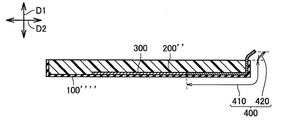
우선, 본 발명의 실시예 1에 따른 부품 모듈에 대해서 상기 도 1을 참조하면서 설명한다. 도 1에 나타낸 부품 모듈은 터치 입력장치이다. 이 부품 모듈은, 베이스(100)와, 수지부(200)와, 터치 센서(300)(부품)와, 외부 접속부(400)를 포함하고 있다. 이하, 상기 부품 모듈의 각 구성 요소에 대해서 상세히 설명한다. 또, 도 1에 나타낸 (D1)은 부품 모듈 및 수지부(200)의 두께 방향이며, (D2)는 부품 모듈의 길이 방향이다. (D1)은 (D2)와 직교하고 있다. 도시하지 않은 부품 모듈의 폭 방향(短手方向)은 (D1), (D2)와 직교하고 있다.First, a component module according to Embodiment 1 of the present invention will be described with reference to FIG. The component module shown in FIG. 1 is a touch input device. This component module includes a
베이스(100)는 가요성을 지니는 대략 직사각 형상의 투명 수지 필름(예를 들어, PET(폴리에틸렌테레프탈레이트) 필름이나 아크릴 필름 등)이다. 베이스(100)는, 베이스(100)의 내면인 제1면(101)과, 베이스(100)의 외면인 제2면(102)을 가지고 있다. 베이스(100)의 제1면(101)에는, 전체 영역 또는 일부의 영역(예를 들어, 외주 영역 또는 길이 방향(D2) 또는 폭 방향의 한 방향의 단부 등)에 장식 인쇄가 실시되어 있다.The
수지부(200)는, 베이스(100)의 제1면(101) 상에 형성된 단면(斷面)에서 보아서 대략 U자 형상의 절연성을 지니는 열가소성 수지 또는 열경화성 수지(예를 들어, PC(폴리카보네이트), PMMA(폴리메타크릴산메틸 수지), 에폭시 수지 등)이다. 수지부(200)가 베이스(100)의 제1면(101) 상에 설치됨으로써, 베이스(100)는, 일반적으로 수지부(200)에 밀착 또는 동화되어, 수지부(200)를 따라서 대략 역U자 형상으로 만곡된 상태로 경질화되어 있다(가요성을 상실하고 있다). 베이스(100)의 제2면(102)의 평탄한 중앙부가 부품 모듈의 터치 입력면이다.The
터치 센서(300)는 강성 또는 플렉시블(flexible)한(가요성을 지니는) 대략 직사각 형상의 시트 형상의 정전용량 방식 터치 패널로서, 베이스(100)의 터치 입력면에 접촉하는 손가락 등의 검출 대상을 검출가능하다. 터치 센서(300)는, 베이스(100)의 중앙부의 제1면(101) 상에 고착되는 동시에, 수지부(200)에 매립되어 있다. 터치 센서(300)는 베이스(100)의 터치 입력면에 대해서 대략 평행하다.The
터치 센서(300)가 강성의 투명 시트 형상일 경우, 하기 1) 내지 3)의 구성으로 하는 것이 가능하다. 터치 센서(300)가 플렉시블한 투명 시트 형상일 경우(즉, 필름 센서일 경우), 하기 4 내지 6)의 구성으로 하는 것이 가능하다.When the
1) 터치 센서(300)가, 두께 방향(D1)의 제1, 제2면을 지니는 제1투명 기판과, 상기 제1투명 기판의 제1면상에 형성된 복수의 제1투명 전극과, 상기 제1투명 기판의 제2면 상에 형성된 복수의 제2투명 전극을 가진 구성이다.1) The
2) 터치 센서(300)가, 제1투명 기판과, 이 제1투명 기판 상에 형성된 복수의 제1투명 전극과, 상기 제1투명 전극을 덮도록 상기 제1투명 기판 상에 형성된 절연층과, 이 절연층 상에 형성된 복수의 제2투명 전극을 가진 구성이다.2) The
3) 터치 센서(300)가, 제1면을 지니는 제1투명 기판과, 이 제1투명 기판의 제1면에 대향하는 제1면을 지니는 제2투명 기판과, 상기 제1투명 기판의 제1면에 설치된 복수의 제1투명 전극과, 상기 제2투명 기판의 제1면에 설치된 복수의 제2투명 전극을 가진 구성이다.3) The
4) 터치 센서(300)가, 두께 방향(D1)의 제1, 제2면을 지니는 플렉시블한 절연성을 지니는 제1투명 필름과, 상기 제1투명 필름의 제1면에 설치된 복수의 제1투명 전극과, 상기 제1투명 필름의 제2면에 설치된 복수의 제2투명 전극을 가진 구성이다.4) The
5) 터치 센서(300)가, 플렉시블한 절연성을 지니는 제1투명 필름과, 이 제1투명 필름 상에 형성된 복수의 제1투명 전극과, 상기 제1투명 전극을 덮도록 상기 제1투명 필름 상에 형성된 플렉시블한 절연성을 지니는 제2투명 필름과, 이 제2투명 필름 상에 형성된 복수의 제2투명 전극을 가진 구성이다.5) The
6) 터치 센서(300)가, 제1면을 지니는 플렉시블한 절연성을 지니는 제1투명 필름과, 제1투명 필름의 제1면에 대향하는 제1면을 지니는 플렉시블한 절연성을 지니는 제2투명 필름과, 상기 제1투명 필름의 제1면에 설치된 복수의 제1투명 전극과, 상기 제2투명 필름의 제1면에 설치된 복수의 제2투명 전극을 가진 구성이다.6) The
외부 접속부(400)는 가요성을 지니고 있다. 구체적으로는, 외부 접속부(400)는 플렉시블 인쇄 기판 또는 플렉시블한 절연성을 지니는 투명 필름이다. 외부 접속부(400)는 매몰부(410)와 도출부(420)를 가지고 있다. 매몰부(410)는, 외부 접속부(400)의 베이스(100)의 제1면(101) 상에 고착되고 또한 수지부(200) 내에 매립된 부분으로서, 외부 접속부(400)의 길이 방향의 제1단부를 가지고 있다. 외부 접속부(400)가 플렉시블 인쇄 기판일 경우, 외부 접속부(400)의 제1단부가 터치 센서(300)의 제1, 제2투명 기판 중 적어도 한쪽 또는 제1, 제2투명 필름 중 적어도 한쪽에 접속되어 있다. 플렉시블 인쇄 기판의 복수의 도전 라인은 제1, 제2투명 전극에 접속되어 있다. 외부 접속부(400)가 투명 필름일 경우, 외부 접속부(400)의 제1단부가 터치 센서(300)의 제1, 제2투명 기판 중 적어도 한쪽에 접속 또는 제1, 제2투명 필름 중 적어도 한쪽에 일체적으로 연접되어 있다. 투명 필름의 복수의 도전 라인은 제1, 제2투명 전극에 접속되어 있다. 매몰부(410)는 터치 센서(300)로부터 베이스(100)의 단부까지 해당 베이스(100)의 제1면(101) 상을 따라서 뻗고 있다. 도출부(420)는, 외부 접속부(400)의 매몰부(410) 이외의 부분으로서, 매몰부(410)에 연속하고 있다. 도출부(420)가 수지부(200)의 단부면(端面)으로부터 도출되고 있다. 또, 도출부(420)는 외부 접속부(400)의 길이 방향의 제2단부를 가지고 있다.The
이하, 전술한 부품 모듈의 제조에 이용되는 제1, 제2금형(10), (20)에 대해서 상기 도 2를 참조하면서 설명한다. 제1금형(10)은 볼록부(11)와 스풀(spool)(12)과 제1, 제2분할면(13), (14)을 가지고 있다. 볼록부(11)는 제1금형(20)에 두께 방향(D1)의 한쪽(도시한 아래쪽)으로 돌출 설치되어 있다. 스풀(12)은, 제1금형(10)을 두께 방향(D1)으로 관통하고 있다. 제1분할면(13)은 볼록부(11)의 길이 방향(D2)의 한쪽 측에 위치하고 있고, 제2분할면(14)은 볼록부(11)의 길이 방향(D2)의 다른 쪽 측에 위치하고 있다. 제2분할면(14)의 높이 위치가, 외부 접속부(400)의 도출부(420)의 두께 치수만큼, 제1분할면(13)의 높이 위치보다도 두께 방향(D1)의 다른 쪽(도시한 위쪽)에 위치하고 있다.Hereinafter, the 1st,
제2금형(20)은, 볼록부(11)가 삽입가능한 오목부(21)와, 제1, 제2분할면(22), (23)을 가지고 있다. 오목부(21)의 두께 방향(D1)의 치수(깊이 치수)는 볼록부(11)의 두께 방향(D1)의 치수(높이 치수)보다도 크다. 제1, 제2금형(10), (20)이 체결된(즉, 조합된) 상태에서, 볼록부(11)가 오목부(21)에 삽입되어, 볼록부(11)와 오목부(21)에 의해 공간이 구획된다. 해당 공간이 제1, 제2금형(10), (20)의 공동으로 된다. 공동의 형상은, 부품 모듈의 도출부(420)를 제외한 외형에 대응한 형상으로 되어 있다. 제1분할면(22)은 오목부(21)의 길이 방향(D2)의 한쪽 측에 위치하고 있고, 제2분할면(23)은 오목부(21)의 길이 방향(D2)의 다른 쪽 측에 위치하고 있다. 제1, 제2분할면(22), (23)의 높이 위치는 동일하다. 제1, 제2금형(10), (20)이 체결된 상태에서, 제1분할면(13), (22)이 서로 맞닿아, 제2분할면(14), (23) 사이에 도출부(420)의 두께 치수분의 간극(G)이 형성된다.The
이하, 상기 부품 모듈을 제1, 제2금형(10), (20)을 이용해서 제조하는 방법에 대해서 도 2를 참조하면서 설명한다. 우선, 베이스(100)와, 외부 접속부(400)가 접속된 터치 센서(300)를 준비한다. 터치 센서(300) 및 외부 접속부(400)의 매몰부(410)를 베이스(100)의 제1면(101) 상에 접착제로 고착시킨다. 이것에 의해, 매몰부(410)가 터치 센서(300)로부터 베이스(100)의 단부까지 베이스(100)를 따라서 배치되고, 도출부(420)가 베이스(100)의 단부로부터 돌출된다.Hereinafter, the method of manufacturing the said component module using the 1st,
그 후, 베이스(100), 터치 센서(300) 및 외부 접속부(400)의 매몰부(410)를 제2금형(20)의 오목부(21)에 삽입한다. 그러면, 베이스(100)가 오목부(21)의 벽면의 형상을 따라서 단면에서 보아서 대략 U자 형상으로 만곡되고, 이에 따라서 매몰부(410)도 만곡된다. 이와 함께, 외부 접속부(400)의 도출부(420)를 제1, 제2금형(10), (20)의 제2분할면(14), (23) 사이에 배치시킨다.Thereafter, the buried
그 후, 제1, 제2금형(10), (20)을 상대적으로 접근시켜, 제1, 제2금형(10), (20)을 체결한다. 그러면, 제1금형(10)의 볼록부(11)가 제2금형(20)의 오목부(21)에 삽입된다. 이것에 의해, 볼록부(11)와 오목부(21) 사이에 상기 공동이 형성되고, 해당 공동 내에 베이스(100), 터치 센서(300) 및 외부 접속부(400)의 매몰부(410)가 수용된다. 이때, 제1, 제2금형(10), (20)의 제1분할면(13), (22)이 서로 맞닿고, 외부 접속부(400)의 도출부(420)가 제1, 제2금형(10), (20)의 제2분할면(14), (23) 사이에 끼여 유지된다.Thereafter, the first and
그 후, 제1금형(10)의 스풀(12)을 통해서 수지(R)가 공동 내의 베이스(100) 상에 사출되어, 해당 공동 내에 충전된다. 이것에 의해, 터치 센서(300) 및 외부 접속부(400)의 매몰부(410)가 베이스(100) 상에서 수지(R)에 매립된다. 이 수지(R)를 경화시킨다. 경화된 수지(R)가 수지부(200)로 된다. 이때, 베이스(100)가 수지부(200)에 밀착 또는 동화되어, 경질화된다. 이와 같이 해서 베이스(100) 상의 수지부(200)에 터치 센서(300) 및 외부 접속부(400)의 매몰부(410)가 삽입 성형되고, 외부 접속부(400)의 도출부(420)가 수지부(200)의 단부면으로부터 도출된다. 그 후, 제1, 제2금형(10), (20)을 상대적으로 이반시켜, 전술한 바와 같이 제조된 부품 모듈을 꺼낸다.Thereafter, the resin R is injected onto the base 100 in the cavity through the
이상과 같은 부품 모듈에 의한 경우, 외부 접속부(400)의 매몰부(410)가, 수지부(200)에 매립되어, 터치 센서(300)로부터 베이스(100)의 단부까지 해당 베이스(100) 상을 따라서 뻗고 있다. 외부 접속부(400)의 도출부(420)가, 수지부(200)의 단부면으로부터 도출되고 있다. 이 때문에, 삽입 성형 시에 있어서, 베이스(100), 터치 센서(300) 및 외부 접속부(400)의 매몰부(410)를 제1, 제2금형(10), (20)의 공동 내에 배치하는 동시에, 해당 제1, 제2금형(10), (20)에 의해 외부 접속부(400)의 도출부(420)를 끼워 유지시킬 수 있다. 따라서, 상기 부품 모듈은, 외부 접속부(400)의 도출부(420)를 금형의 수용 오목부에 삽입하는 일 없이, 제조된다. 게다가, 터치 센서(300)와 외부 접속부(400)의 매몰부(410)가 베이스(100) 상에 고착되고, 외부 접속부(400)의 도출부(420)가 제1, 제2금형(10), (20) 사이에 끼여 유지되어 있으므로, 공동 내에 사출되는 수지(R)에 의해서, 외부 접속부(400)가 눌려서, 외부 접속부(400)가 이동하는 것을 억제할 수 있다.In the case of the component module as described above, the buried
실시예Example 2 2
다음에, 본 발명의 실시예 2에 따른 부품 모듈에 대해서 상기 도 3을 참조하면서 설명한다. 도 3에 나타낸 부품 모듈은, 베이스(100')의 형상이 베이스(100)의 형상과 상이한 이외에, 실시예 1의 부품 모듈과 같은 구성이다. 이하, 전술한 상위점에 대해서 상세히 설명하고, 실시예 1과 중복되는 설명에 대해서는 생략한다. 한편, 베이스에 대해서는 "'"를 붙여서 실시예 1의 베이스와 구별한다. 도 3에도 상기 (D1), (D2)가 표시되어 있다.Next, a component module according to
베이스(100')는, 가요성을 지니는 대략 직사각 형상의 투명 수지 필름(예를 들어, PET(폴리에틸렌테레프탈레이트) 필름이나 아크릴 필름 등)이다. 베이스(100')는, 제1, 제2면(101'), (102')과, 베이스 본체(110')와, 고착부(120')를 가지고 있다. 제1면(101')은 베이스(100')의 내면이다. 제2면(102')은 베이스(100')의 외면이다. 베이스 본체(110')는, 베이스(100')의 수지부(200)에 고정된 부분이다. 베이스 본체(110')의 제1면(101')에는, 전체 영역 또는 일부의 영역(예를 들어, 외주 영역 또는 길이 방향(D2) 또는 폭 방향의 한 방향의 단부 등)에 장식 인쇄가 실시되어 있다. 고착부(120')는 베이스(100')의 수지부(200)에 고정되지 않고 있는 부분이며, 베이스 본체(110')에 연속하고 있다. 즉, 고착부(120')는 수지부(200)로부터 뻗어 나오고 있다.The base 100 'is a substantially rectangular transparent resin film (eg, PET (polyethylene terephthalate) film, acrylic film, etc.) having flexibility. The base 100 'has first and second surfaces 101', 102 ', a base body 110', and a fixing portion 120 '. The first surface 101 'is the inner surface of the base 100'. The second surface 102 'is the outer surface of the base 100'. The base main body 110 'is a part fixed to the
베이스 본체(110')의 제1면(101') 상에는, 수지부(200)가 형성되어 있다. 이 수지부(200)가 베이스 본체(110')의 제1면(101') 상에 형성됨으로써, 베이스 본체(110')는, 일반적으로 수지부(200)에 밀착 또는 동화되어, 수지부(200)를 따라서 대략 역U자 형상으로 만곡된 상태로 경질화되고 있다(수지부(200)에 고정되어, 가요성을 상실하고 있다). 베이스 본체(110')의 제2면(102')의 평탄한 중앙부가 부품 모듈의 터치 입력면이다.The
베이스 본체(110')의 제1면(101')의 중앙부 상에는, 터치 센서(300)가 고착되고, 수지부(200)에 매립되어 있다. 터치 센서(300)는 터치 입력면에 대해서 대략 평행하다. 또, 베이스 본체(110')의 제1면(101') 상에는, 터치 센서(300)에 접속된 외부 접속부(400)의 매몰부(410)가 고착되고, 수지부(200)에 매립되어 있다. 매몰부(410)는 터치 센서(300)로부터 베이스 본체(110')와 고착부(120')의 경계까지 해당 베이스 본체(110')의 제1면(101') 상을 따라서 뻗고 있다. 도출부(420)는, 고착부(120')의 제1면(101') 상에 고착되고 또한 수지부(200)의 단부면으로부터 도출되고 있다. 도출부(420)는 고착부(120')의 제1면(101') 상을 따라서 뻗고 있다.On the central portion of the
전술한 부품 모듈의 제조에 이용하는 제1금형(10')은, 상기 도 4에 나타낸 바와 같이, 제2분할면(14')의 높이 위치가 후술하는 바와 같이 제2분할면(14)의 높이 위치와 상이한 이외에, 제1금형(10)과 같은 구성이다. 이하, 전술한 상위점에 대해서 상세히 설명하고, 실시예 1과 중복되는 설명에 대해서는 생략한다. 또, 제1금형에 대해서는 "'"를 붙여서 제1금형(10)과 구별한다. 또한, 제2금형(20)은 실시예 1과 같은 것이다. 제1, 제2금형(10'), (20)의 공동의 형상은, 부품 모듈의 도출부(420) 및 고착부(120')를 제외한 외형에 대응한 형상으로 되어 있다.As shown in FIG. 4, as for the 1st mold 10 'used for manufacture of a component module mentioned above, the height of the 2nd dividing surface 14' is high, as will be mentioned later. In addition to being different from the position, it is the same configuration as the
제2분할면(14')의 높이 위치는, 베이스(100')의 고착부(120') 및 외부 접속부(400)의 도출부(420)의 두께 치수만큼, 제1분할면(13)'의 높이 위치보다도 두께 방향(D1)의 다른 쪽(도시한 위쪽)에 위치하고 있다. 제1, 제2금형(10'), (20)이 체결된 상태에서, 제1분할면(13'), (22)이 서로 맞닿고, 제2분할면(14'), (23) 사이에 고착부(120') 및 도출부(420)의 두께 치수분의 간극(G')이 형성된다.The height position of the
이하, 상기 부품 모듈을 제1, 제2금형(10'), (20)을 이용해서 제조하는 방법에 대해서 도 4를 참조하면서 설명한다. 우선, 베이스(100')와, 외부 접속부(400)가 접속된 터치 센서(300)를 준비한다. 터치 센서(300) 및 외부 접속부(400)의 매몰부(410)를 베이스(100')의 베이스 본체(110')의 제1면(101') 상에 접착제로 고착시키는 동시에, 외부 접속부(400)의 도출부(420)를 베이스(100')의 고착부(120')의 제1면(101') 상에 접착제로 고착시킨다. 이것에 의해, 매몰부(410)가 터치 센서(300)로부터 상기 경계까지 베이스 본체(110')를 따라서 배치되고, 도출부(420)가 고착부(120')를 따라서 배치된다.Hereinafter, the method of manufacturing the said component module using the 1st,
그 후, 베이스(100')의 베이스 본체(110'), 터치 센서(300) 및 외부 접속부(400)의 매몰부(410)를 제2금형(20)의 오목부(21)에 삽입한다. 그러면, 베이스 본체(110')가 오목부(21)의 벽면의 형상을 따라서 단면에서 보아서 대략 U자 형상으로 만곡되고, 이에 따라서 매몰부(410)도 만곡된다. 이것과 함께, 베이스(100')의 고착부(120') 및 외부 접속부(400)의 도출부(420)를 제1, 제2금형(10'), (20)의 제2분할면(14'), (23) 사이에 배치시킨다.Thereafter, the base
그 후, 제1, 제2금형(10'), (20)을 상대적으로 접근시켜, 제1, 제2금형(10'), (20)을 체결한다. 그러면, 제1금형(10')의 볼록부(11')가 제2금형(20)의 오목부(21)에 삽입된다. 이것에 의해, 볼록부(11')와 오목부(21) 사이에 공동이 형성되고, 해당 공동 내에 베이스 본체(110'), 터치 센서(300) 및 외부 접속부(400)의 매몰부(410)가 수용된다. 이때, 제1, 제2금형(10'), (20)의 제1분할면(13'), (22)이 서로 맞닿고, 고착부(120') 및 도출부(420)가 제1, 제2금형(10'), (20)의 제2분할면(14'), (23) 사이에 끼여 유지된다.Thereafter, the first and
그 후, 제1금형(10')의 스풀(12')을 통해서 수지(R)가 공동 내의 베이스 본체(110') 상에 사출되어, 해당 공동 내에 충전된다. 이것에 의해, 터치 센서(300) 및 외부 접속부(400)의 매몰부(410)가 베이스 본체(110') 상에 수지(R)에 매립된다. 이 수지(R)를 경화시킨다. 경화된 수지(R)가 수지부(200)로 된다. 이때, 베이스 본체(110')가 수지부(200)에 밀착 또는 동화되어, 경질화된다. 이와 같이 해서 베이스 본체(110') 상의 수지부(200)에 터치 센서(300) 및 외부 접속부(400)의 매몰부(410)가 삽입 성형되어, 외부 접속부(400)의 도출부(420)가 수지부(200)의 단부면으로부터 도출된다. 그 후, 제1, 제2금형(10'), (20)을 상대적으로 이반시켜, 전술한 바와 같이 제조된 부품 모듈을 꺼낸다.Thereafter, the resin R is injected onto the base body 110 'in the cavity through the spool 12' of the first mold 10 'and filled in the cavity. Thereby, the embedding
이상과 같은 부품 모듈에 의한 경우, 외부 접속부(400)의 매몰부(410)가, 수지부(200)에 매립되어, 터치 센서(300)로부터 베이스 본체(110')와 고착부(120')과의 경계까지 해당 베이스 본체(110') 상을 따라서 뻗고 있다. 외부 접속부(400)의 도출부(420)가, 고착부(120')에 고착되고, 수지부(200)의 단부면으로부터 도출되고 있다. 이 때문에, 삽입 성형 시에 있어서, 베이스 본체(110'), 터치 센서(300) 및 외부 접속부(400)의 매몰부(410)를 제1, 제2금형(10'), (20)의 공동 내에 배치하는 동시에, 해당 제1, 제2금형(10'), (20) 사이에 고착부(120') 및 도출부(420)를 끼워 유지시킬 수 있다. 따라서, 상기 부품 모듈은, 외부 접속부(400)의 도출부(420)를 금형의 수용 오목부에 삽입하는 일 없이, 제조된다. 게다가, 터치 센서(300)와 외부 접속부(400)의 매몰부(410)가 베이스 본체(110') 상에 고착되고, 외부 접속부(400)의 도출부(420)가 제1, 제2금형(10'), (20) 사이에 끼여 유지되어 있으므로, 공동 내에 사출되는 수지(R)에 의해서, 외부 접속부(400)가 눌려서, 외부 접속부(400)가 이동하는 것을 억제할 수 있다. 또한, 도출부(420)가 고착부(120')와 함께, 제1, 제2금형(10'), (20) 사이에 끼여 유지되므로, 도출부(420)가 고착부(120')에 의해서 제2금형(20)으로부터 보호된다.In the case of the component module described above, the buried
실시예Example 3 3
다음에, 본 발명의 실시예 3에 따른 부품 모듈에 대해서 상기 도 5를 참조하면서 설명한다. 도 5에 나타낸 부품 모듈은, 베이스(100'')의 형상, 수지부(200')의 구성 및 외부 접속부(400')의 구성의 점에서, 실시예 1의 부품 모듈과 상이하다. 이외에 대해서는, 상기 부품 모듈은 실시예 1의 부품 모듈과 같은 구성이다. 이하, 전술한 상위점에 대해서 상세히 설명하고, 실시예 1과 중복되는 설명에 대해서는 생략한다. 또한, 베이스에 대해서는 "''"를 붙여서 실시예 1의 베이스와 구별한다. 수지부 및 외부 접속부에 대해서는 "'"를 붙여서 실시예 1의 수지부 및 외부 접속부와 구별한다. 도 5에도 상기 (D1), (D2)가 표시되어 있다.Next, a component module according to Embodiment 3 of the present invention will be described with reference to FIG. The component module shown in FIG. 5 differs from the component module of Example 1 by the point of the shape of the base 100 ", the structure of the resin part 200 ', and the structure of the external connection part 400'. In other respects, the component module has the same configuration as the component module of the first embodiment. Hereinafter, the above difference is demonstrated in detail, and the description overlapping with Example 1 is abbreviate | omitted. In addition, about a base, "" "is attached | subjected and it distinguishes from the base of Example 1. "'" Is attached | subjected about a resin part and an external connection part, and it distinguishes from the resin part and external connection part of Example 1. FIG. (D1) and (D2) are also shown in FIG.
베이스(100'')는 가요성을 지니는 대략 직사각 형상의 투명 수지 필름(예를 들어, PET(폴리에틸렌테레프탈레이트) 필름이나 아크릴 필름 등)이며, 길이 방향(D2)의 치수가 베이스(100)의 길이 방향(D2)의 치수보다도 짧다. 베이스(100'')는, 베이스(100'')의 내면인 제1면(101)과, 베이스(100'')의 외면인 제2면(102'')을 가지고 있다. 베이스(100'')의 제1면(101'')에는, 전체 영역 또는 일부의 영역(예를 들어, 외주 영역 또는 길이 방향(D2) 또는 폭 방향 중 한쪽의 단부 등)에 장식 인쇄가 실시되어 있다.The base 100 ″ is a substantially rectangular transparent resin film (eg, a PET (polyethylene terephthalate) film, an acrylic film, etc.) having flexibility, and the dimension in the longitudinal direction D2 is determined by the length of the
수지부(200')는 단면에서 보아서 대략 U자 형상의 절연성을 지니는 열가소성 수지 또는 열경화성 수지(예를 들어, PC(폴리카보네이트), PMMA(폴리메타크릴산메틸 수지), 에폭시 수지 등)이다. 수지부(200')는 수지부 본체(210')와 돌출부(220'), (230')를 가지고 있다. 수지부 본체(210')는 수지부(200')의 베이스(100'')의 제1면(101'') 상에 형성된 부분이다. 수지부 본체(210')가 베이스(100'')의 제1면(101'') 상에 설치됨으로써, 베이스(100'')는, 일반적으로 수지부 본체(210')에 밀착 또는 동화되어, 수지부 본체(210')를 따라서 대략 역U자 형상으로 만곡된 상태로 경질화되고 있다(가요성을 상실하고 있다). 베이스(100'')의 제1면(101'')의 중앙부 상에는, 터치 센서(300)가 고착되고, 수지부(200')의 수지부 본체(210')에 매립되어 있다. 베이스(100'')의 제2면(102'')의 평탄한 중앙부가 부품 모듈의 터치 입력면이다. 터치 센서(300)는 터치 입력면에 대해서 대략 평행하다. 돌출부(220'), (230')는, 수지부 본체(210')의 길이 방향(D2)의 양단부에 연접되어, 두께 방향(D1)으로 만곡되면서 뻗고 있다. 즉, 돌출부(220'), (230')는 수지부(200')의 베이스(100'')의 제1면(101'') 상에 설치되어 있지 않은 부분이다.The
외부 접속부(400')는, 도출부(420')의 구성의 점에서, 외부 접속부(400)와 상이하다. 이것 이외에 대해서는, 외부 접속부(400')는 외부 접속부(400)와 같은 구성이다. 이하, 전술한 상위점에 대해서 상세히 설명하고, 실시예 1과 중복되는 설명에 대해서는 생략한다. 매몰부(410')는 외부 접속부(400')의 베이스(100'')의 제1면(101'') 상에 고착되고 또한 수지부(200') 내에 매립된 부분이다. 도출부(420')는 외부 접속부(400')의 매몰부(410') 이외의 부분이다. 도출부(420')는, 매몰부(410')에 연속하는 고정 단부(421')와, 고정 단부(421')에 연속하는 자유 단부(422')를 가지고 있다. 고정 단부(421')는 수지부(200')의 돌출부(220')에 고착되고 또한 돌출부(220')를 따라서 뻗고 있다. 자유 단부(422')는 수지부(200')의 돌출부(220')의 단부면으로부터 돌출하고 있다.The external connection part 400 'differs from the
전술한 부품 모듈의 제조에 이용하는 제1금형(10)은 실시예 1과 같은 것이다. 제2금형(20')은, 상기 도 6에 나타낸 바와 같이, 오목부(21) 대신에 제1, 제2오목부(21a'), (2lb')를 지니는 점에서, 제2금형(20)과 상이한 이외에, 제2금형(20)과 같은 구성이다. 이하, 전술한 상위점에 대해서 상세히 설명하고, 실시예 1과 중복되는 설명에 대해서는 생략한다. 또한, 제2금형에 대해서는 "'"를 붙여서 제2금형(20)과 구별한다.The
제1오목부(21a')는 볼록부(11)가 삽입가능한 오목부이다. 제2오목부(2lb')는, 제1오목부(21a')의 밑부분에 형성된 오목부로서, 베이스(100'')에 대응한 형상으로 되어 있다. 제1오목부(21a') 및 제2오목부(2lb')의 두께 방향(D1)의 치수(깊이 치수)의 합은, 볼록부(11)의 두께 방향(D1)의 치수(높이 치수)보다도 크다. 제1금형(10), (20')이 체결된 상태에서, 볼록부(11)가 제1오목부(21a')에 삽입되어, 볼록부(11)와 제1, 제2오목부(21a'), (2lb')에 의해 공간이 구획된다. 해당 공간이 제1, 제2금형(10), (20')의 공동으로 된다. 제1, 제2금형(10), (20')의 공동의 형상은, 부품 모듈의 도출부(420')의 자유 단부(422')를 제외한 외형에 대응한 형상으로 되어 있다. 제1, 제2금형(10), (20')이 체결된 상태에서, 제1분할면(13), (22')이 서로 맞닿고, 제2분할면(14), (23') 사이에 도출부(420')의 두께 치수분의 간극(G)이 형성된다.The
이하, 상기 부품 모듈을 제1, 제2금형(10), (20')을 이용해서 제조하는 방법에 대해서 도 6을 참조하면서 설명한다. 우선, 베이스(100'')와, 외부 접속부(400')가 접속된 터치 센서(300)를 준비한다. 터치 센서(300) 및 외부 접속부(400')의 매몰부(410')를 베이스(100'')의 제1면(101'') 상에 접착제로 고착시킨다. 이것에 의해, 매몰부(410')가 터치 센서(300)로부터 베이스(100'')의 단부까지 베이스(100'')를 따라서 배치되고, 도출부(420'')가 베이스(100'')의 단부로부터 돌출된다.Hereinafter, the method of manufacturing the said component module using the 1st,
그 후, 베이스(100'')를 제2금형(20')의 제2오목부(2lb')에 삽입하고, 터치 센서(300) 및 외부 접속부(400')의 매몰부(410')를 제2금형(20')의 제1오목부(21a')에 삽입한다. 그러면, 베이스(100'')가 제2오목부(2lb')의 벽면의 형상을 따라서 단면에서 보아서 대략 U자 형상으로 만곡되고, 이에 따라서 매몰부(410')도 만곡된다. 이것과 함께, 외부 접속부(400')의 도출부(420')의 고정 단부(421')가 제1오목부(21a')의 벽면(공동의 벽면)의 형상을 따라서 만곡된다(상기 벽면을 따라서 배치한다). 이때, 도출부(420')의 자유 단부(422')를 제1, 제2금형(10), (20')의 제2분할면(14), (23') 사이에 배치한다.Thereafter, the base 100 '' is inserted into the second recess 2lb 'of the second mold 20', and the buried portion 410 'of the
그 후, 제1, 제2금형(10), (20')을 상대적으로 접근시켜, 제1, 제2금형(10), (20')을 체결한다. 그러면, 제1금형(10)의 볼록부(11)가 제2금형(20')의 제1오목부(21a')에 삽입된다. 이것에 의해, 볼록부(11)와 제1, 제2오목부(21a'), (2lb')에 의해 상기 공동이 형성되고, 해당 공동 내에 베이스(100''), 터치 센서(300), 외부 접속부(400')의 매몰부(410') 및 외부 접속부(400')의 도출부(420')의 고정 단부(421')가 수용된다. 이때, 제1, 제2금형(10), (20')의 제1분할면(13), (22')이 서로 맞닿고, 도출부(420')의 자유 단부(422')가 제1, 제2금형(10), (20')의 제2분할면(14), (23') 사이에 끼여 유지된다.Thereafter, the first and
그 후, 제1금형(10)의 스풀(12)을 통해서 수지(R)가 공동 내의 베이스(100'') 상에 사출되어, 해당 공동 내에 충전된다. 이것에 의해, 터치 센서(300) 및 외부 접속부(400')의 매몰부(410')가 베이스(100'') 상에 수지(R)에 매립된다. 이것과 함께, 외부 접속부(400')의 도출부(420')의 고정 단부(421')가 수지(R)에 밀착된다. 이 수지(R)를 경화시킨다. 경화된 수지(R)가 수지부(200')로 된다. 이때, 베이스(100'')가 수지부(200')에 밀착 또는 동화되어, 경질화되는 동시에, 외부 접속부(400')의 고정 단부(421')가 수지부(200')에 고착된다. 베이스(100'')가 고착된 부분이 수지부(200')의 수지부 본체(210')로 된다. 고정 단부(421')가 고착된 부분이 수지부(200')의 돌출부(220')로 된다. 수지부(200')의 나머지의 부분이 돌출부(230')로 된다. 이와 같이 해서 베이스(100'') 상의 수지부(200')의 수지부 본체(210')에 터치 센서(300) 및 외부 접속부(400')의 매몰부(410')가 삽입 성형되고, 외부 접속부(400')의 도출부(420')의 고정 단부(421')가 돌출부(220')에 고착되며, 자유 단부(422')가 돌출부(220')의 단부면으로부터 도출된다. 그 후, 제1, 제2금형(10), (20')을 상대적으로 이반시켜, 전술한 바와 같이 제조된 부품 모듈을 꺼낸다.Thereafter, the resin R is injected onto the base 100 ″ in the cavity through the
이상과 같은 부품 모듈에 의한 경우, 외부 접속부(400')의 매몰부(410')가 수지부(200')에 매립되고, 터치 센서(300)로부터 베이스(100'')의 단부까지 해당 베이스(100'') 상을 따라서 뻗고 있다. 외부 접속부(400')의 도출부(420')의 고정 단부(421')는, 수지부(200')의 돌출부(220')에 고착되고 또한 해당 돌출부(220')를 따라서 뻗고 있다. 외부 접속부(400')의 도출부(420')의 자유 단부(422')가 돌출부(220')의 단부면으로부터 도출되고 있다. 이 때문에, 삽입 성형 시에 있어서, 베이스(100''), 터치 센서(300) 및 매몰부(410')를 제1, 제2금형(10), (20')의 공동 내에 배치하고, 고정 단부(421')를 공동의 벽면(제2금형(20')의 제1오목부(21a')의 벽면)을 따라 배치하며, 해당 제1, 제2금형(10), (20') 사이에 도출부(420')의 자유 단부(422')를 끼워 유지시킬 수 있다. 따라서, 상기 부품 모듈은, 외부 접속부(400')의 도출부(420')를 금형의 수용 오목부에 삽입하는 일 없이, 제조된다. 게다가, 터치 센서(300)와 외부 접속부(400')의 매몰부(410')가 베이스(100'') 상에 고착되고, 고정 단부(421')가 공동의 벽면을 따라서 배치되어 있다. 자유 단부(422')는 제1, 제2금형(10), (20') 사이에 끼여 유지되어 있다. 이 때문에, 공동 내에 사출되는 수지(R)에 의해서, 외부 접속부(400')의 매몰부(410')가 눌려서, 외부 접속부(400')가 이동하는 것을 억제할 수 있다.In the case of the component module described above, the buried portion 410 'of the external connection portion 400' is embedded in the resin portion 200 ', and the base is extended from the
실시예Example 4 4
다음에, 본 발명의 실시예 4에 따른 부품 모듈에 대해서 상기 도 7을 참조하면서 설명한다. 도 7에 나타낸 부품 모듈은 터치 입력장치이다. 이 부품 모듈은, 베이스(500)와, 수지부(600)와, 터치 센서(300)(센서)와, 외부 접속부(700)를 구비하고 있다. 이하, 상기 부품 모듈의 각 구성 요소에 대해서 상세히 설명한다. 한편, 도 7에 나타낸 (D1)은 부품 모듈 및 수지부(600)의 두께 방향이며, (D2)는 부품 모듈의 길이 방향이다. (D1)은 (D2)와 직교하고 있다. 도시하지 않은 부품 모듈의 폭 방향은 (D1), (D2)와 직교하고 있다.Next, a component module according to Embodiment 4 of the present invention will be described with reference to FIG. The component module shown in FIG. 7 is a touch input device. This component module is provided with the
베이스(500)는 필름(510)과 수지 블록(520)을 가지고 있다. 필름(510)은 가요성을 지니는 대략 직사각 형상의 투명 수지 필름(예를 들어, PET(폴리에틸렌테레프탈레이트) 필름이나 아크릴 필름 등)이다. 필름(510)은 필름(510)의 내면인 제1면(511)과 필름(510)의 외면인 제2면(512)을 가지고 있다. 필름(510)의 제1면(511)에는 전체 영역 또는 일부의 영역(예를 들어, 외주 영역 또는 길이 방향(D2) 또는 폭 방향의 한 방향의 단부 등)에 장식 인쇄가 실시되어 있다.The
수지 블록(520)은, 필름(510)의 제1면(511) 상에 형성된 단면에서 보아서 대략 U자 형상의 절연성 및 투광성을 지니는 열가소성 수지 또는 열경화성 수지(예를 들어, PC(폴리카보네이트), PMMA(폴리메타크릴산메틸 수지), 에폭시 수지 등)이다. 수지 블록(520)이 필름(510)의 제1면(511) 상에 설치됨으로써, 필름(510)은, 일반적으로 수지 블록(520)에 밀착 또는 동화되어, 수지 블록(520)에 따라 대략 역U자 형상으로 만곡된 상태로 경질화되고 있다(가요성을 상실하고 있다). 필름(510)의 제2면(512)의 평탄한 중앙부가 부품 모듈의 터치 입력면이다. 수지 블록(520)은, 제1면(521)과, 제1면(521)의 반대측의 제2면(522)과, 제1, 제2면(521), (522)에 직교하는 단부면(523), (524)을 가지고 있다. 제2면(522)이 필름(510)에 고착되어 있다. 제1면(521)의 중앙부에는, 터치 센서(300)가 고착되고 또한 수지부(600)의 후술하는 수지부 본체(610)에 매립되어 있다. 터치 센서(300)는 베이스(100)의 터치 입력면에 대해서 대략 평행하다.The
수지부(600)는, 단면에서 보아서 대략 U자 형상의 절연성을 지니는 열가소성 수지 또는 열경화성 수지(예를 들어, PC(폴리카보네이트), PMMA(폴리메타크릴산메틸 수지), 에폭시 수지 등)이다. 수지부(600)는 수지부 본체(610)와 돌출부(620), (630)를 가지고 있다. 수지부 본체(610)는 수지부(600)의 수지 블록(520)의 제1면(521) 상에 형성된 부분이다. 돌출부(620), (630)는 수지부 본체(610)의 길이 방향(D2)의 양단부에 연접되어, 두께 방향(D1)으로 뻗고 있다(위쪽으로 뻗고 있다). 즉, 돌출부(620), (630)는 수지부(600)의 수지 블록(520) 제1면(521) 상에 설치되어 있지 않은 부분이다.The
외부 접속부(700)는 가요성을 지니고 있다. 구체적으로는, 외부 접속부(700)는 플렉시블 인쇄 기판 또는 플렉시블한 절연성을 지니는 투명 필름이다. 외부 접속부(700)는 매몰부(710)와 도출부(720)를 가지고 있다. 매몰부(710)는 외부 접속부(700)의 수지 블록(520)의 제1면(521) 상에 고착되고 또한 수지부(600)의 수지부 본체(610) 내에 매립된 부분으로서, 외부 접속부(700)의 길이 방향의 제1단부를 가지고 있다. 외부 접속부(700)의 제1단부는 실시예 1의 외부 접속부(400)의 제1단부와 같이 터치 센서(300)에 접속되어 있다. 매몰부(710)는 터치 센서(300)로부터 수지 블록(520)의 단부면(523)까지 해당 수지 블록(520)의 제1면(521) 상을 따라서 뻗고 있다.The
도출부(720)는 외부 접속부(700)의 매몰부(710) 이외의 부분이다. 도출부(720)는 고정 단부(721)와 자유 단부(722)를 가지고 있다. 고정 단부(721)는 매몰부(710)에 연속하고 있고 또한 수지부(600)의 수지부 본체(610)로부터 도출되어 있다. 이 고정 단부(721)는 수지부(600)의 돌출부(620)의 외면에 고착되고 또한 돌출부(620)를 따라서 뻗고 있다. 자유 단부(722)는 고정 단부(721)에 연속하고 있다. 또한, 자유 단부(722)는 외부 접속부(700)의 길이 방향의 제2단부를 가지고 있다.The
이하, 전술한 부품 모듈의 제조에 이용하는 제1, 제2금형(30), (40)에 대해서 상기 도 8을 참조하면서 설명한다. 제1금형(30)은 볼록부(31)와 스풀(32)과 제1, 제2분할면(33), (34)과 제1, 제2오목부(35), (36)를 가지고 있다. 볼록부(31)은 제1금형(40)에 두께 방향(D1)의 한쪽(도시한 아래쪽)에 돌출 설치되어 있다. 스풀(32)은 제1금형(30)을 두께 방향(D1)으로 관통하고 있다. 제1분할면(33)은 볼록부(31)의 길이 방향(D2)의 한쪽 측에 위치하고 있고, 제2분할면(34)은 볼록부(31)의 길이 방향(D2)의 다른 쪽 측에 위치하고 있다. 제2분할면(34)의 높이 위치가, 외부 접속부(700)의 도출부(720)의 두께 치수만큼, 제1분할면(33)의 높이 위치보다도 두께 방향(D1)의 다른 쪽(도시한 위쪽)에 위치하고 있다. 제1, 제2오목부(35), (36)는, 볼록부(31)와 제1, 제2분할면(33), (34) 사이에 형성되어, 두께 방향(D1)의 다른 쪽(도시한 위쪽)으로 뻗고 있다.Hereinafter, the 1st,
제2금형(40)은 볼록부(31)가 삽입가능한 오목부(41)과, 제1, 제2분할면(43), (23)을 가지고 있다. 오목부(41)의 두께 방향(D1)의 치수(깊이 치수)는 볼록부(31)의 두께 방향(D1)의 치수(높이 치수)보다도 크다. 제1, 제2금형(30), (40)이 조합된 상태(체결된 상태)에서, 볼록부(31)가 오목부(41)에 삽입되고 또한 제1, 제2오목부(35), (36)가 오목부(41)에 연통한다. 이 상태에서, 볼록부(31), 제1, 제2오목부(35), (36) 및 오목부(41)에 의해 공간이 구획된다. 해당 공간이 제1, 제2금형(30), (40)의 공동으로 된다. 공동의 형상은 부품 모듈의 도출부(720)를 제외한 외형에 대응한 형상으로 되어 있다. 제1분할면(42)은 오목부(41)의 길이 방향(D2)의 한쪽 측에 위치하고 있고, 제2분할면(43)은 오목부(41)의 길이 방향(D2)의 다른 쪽 측에 위치하고 있다. 제1, 제2분할면(42), (43)의 높이 위치는 동일하다. 제1, 제2금형(30), (40)이 체결된 상태에서, 제1분할면(33), (42)이 서로 맞닿고, 제2분할면(34), (43) 사이에 도출부(720)의 두께 치수분의 간극(G)이 형성된다.The
이하, 도시하지 않은 금형을 이용해서 베이스(500)를 작성하는 방법에 대해서 설명한다. 우선, 상기 금형의 공동 내에 필름(510)을 수용한다. 그 후, 공동 내의 필름(510) 상에 수지를 사출한다. 경화된 상기 수지가 수지 블록(520)으로 된다. 이때, 필름(510)이 수지 블록(520)에 밀착 또는 동화되어, 경질화된다. 이와 같이 해서 필름(510) 상에 수지 블록(520)이 수지성형된다.Hereinafter, the method of making the base 500 using the metal mold | die which is not shown in figure is demonstrated. First, the
이하, 상기 부품 모듈을 제1, 제2금형(30), (40)을 이용해서 제조하는 방법에 대해서 도 8을 참조하면서 설명한다. 우선, 베이스(500)와 외부 접속부(700)가 접속된 터치 센서(300)를 준비한다. 터치 센서(300) 및 외부 접속부(700)의 매몰부(710)를 베이스(500)의 수지 블록(520)의 제1면(521) 상에 접착제로 고착시킨다. 이것에 의해, 매몰부(710)가 터치 센서(300)로부터 수지 블록(520)의 단부까지 수지 블록(520)을 따라서 배치되고, 도출부(720)가 수지 블록(520)의 단부로부터 돌출된다.Hereinafter, the method of manufacturing the said component module using the 1st,
그 후, 베이스(500)를 제2금형(40)의 오목부(41)에 끼워맞춤시킨다. 이에 따라서, 베이스(500)에 고착된 터치 센서(300) 및 외부 접속부(700)의 매몰부(710)가 오목부(41)에 수용된다. 그러면, 베이스(500)의 수지 블록(520)의 단부면(524), (523)이 제1금형(30)의 제1, 제2분할면(33), (34)의 일부에 대향한다. 이때, 외부 접속부(700)의 도출부(720)를, 수지 블록(520)의 단부면(523)과 제1금형(30)의 제2분할면(34) 사이 및 제1, 제2금형(30), (40)의 제2분할면(34), (43) 사이에 배치시킨다.Thereafter, the
그 후, 제1, 제2금형(30), (40)을 상대적으로 접근시켜, 제1, 제2금형(30), (40)을 체결한다. 그러면, 제1금형(30)의 볼록부(31)가 제2금형(40)의 오목부(41)에 삽입되어, 제1, 제2오목부(35), (36)가 오목부(41)에 연통된다. 볼록부(31), 제1, 제2오목부(35), (36) 및 오목부(41)에 의해 상기 공동이 형성되고, 공동 내에 베이스(500), 터치 센서(300) 및 외부 접속부(700)의 매몰부(710)가 수용된다. 이때, 베이스(500)의 수지 블록(520)의 단부면(524)과 제1금형(30)의 제1분할면(33)의 일부가 맞닿고, 제1, 제2금형(30), (40)의 제1분할면(33), (42)이 서로 맞닿는다. 외부 접속부(700)의 도출부(720)의 고정 단부(721)가, 베이스(500)의 수지 블록(520)의 단부면(523)과 제1금형(30)의 제2분할면(34) 사이에 끼여 유지되고, 해당 도출부(720)의 자유 단부(722)가 제1, 제2금형(30), (40)의 제2분할면(34), (43) 사이에 끼여 유지된다.Thereafter, the first and
그 후, 제1금형(30)의 스풀(32)을 통해서 수지(R)가 공동 내의 베이스(500) 상에 사출되어, 해당 공동 내에 충전된다. 이것에 의해, 터치 센서(300) 및 외부 접속부(700)의 매몰부(710)가 베이스(500) 상에 수지(R)에 매립된다. 이 수지(R)를 경화시킨다. 경화된 수지(R)가 수지부(600)로 된다. 이와 같이 해서 베이스(500) 상의 수지부(600)에 터치 센서(300) 및 외부 접속부(700)의 매몰부(710)가 삽입 성형되어, 외부 접속부(700)의 도출부(720)가 수지부(600)로부터 도출된다. 그 후, 제1, 제2금형(30), (40)을 상대적으로 이반시켜, 전술한 바와 같이 제조된 부품 모듈을 꺼낸다. 그 후, 고정 단부(721)를 수지부(600)의 돌출부(620)의 외면에 접착제로 고착시킨다.Thereafter, the resin R is injected onto the base 500 in the cavity through the
이상과 같은 부품 모듈에 의한 경우, 외부 접속부(700)의 매몰부(710)가, 수지부(600)에 매립되고, 터치 센서(300)로부터 베이스(500)의 단부면(523)까지 해당 베이스(500) 상을 따라서 뻗고 있다. 외부 접속부(700)의 도출부(720)가 수지부(600)로부터 도출되고 있다. 이 때문에, 삽입 성형 시에 있어서, 베이스(500), 터치 센서(300) 및 외부 접속부(700)의 매몰부(710)를 제1, 제2금형(30), (40)의 공동 내에 배치하는 동시에, 외부 접속부(700)의 도출부(720)를 베이스(500)와 제1금형(30) 사이 및 제1, 제2금형(30), (40) 사이에서 끼워 유지시킬 수 있다. 따라서, 상기 부품 모듈은, 외부 접속부(700)의 도출부(720)를 금형의 수용 오목부에 삽입하는 일 없이, 제조된다. 게다가, 터치 센서(300)와 외부 접속부(700)의 매몰부(710)가 베이스(500) 상에 고착되고, 외부 접속부(700)의 도출부(720)가 베이스(500)와 제1금형 사이 및 제1, 제2금형(30), (40) 사이에서 끼여 유지되어 있으므로, 공동 내에 사출되는 수지(R)에 의해, 외부 접속부(700)가 눌려서, 외부 접속부(700)가 이동하는 것을 억제할 수 있다.In the case of the component module described above, the buried
실시예Example 5 5
다음에, 본 발명의 실시예 5에 따른 부품 모듈에 대해서 상기 도 9를 참조하면서 설명한다. 도 9에 나타낸 부품 모듈은 터치 입력장치이다. 이 부품 모듈은 베이스(500')와, 수지부(600')와 터치 센서(300)(센서)와 외부 접속부(700')를 구비하고 있다. 이하, 상기 부품 모듈의 각 구성 요소에 대해서 상세히 설명한다. 또한, 도 9에 나타낸 (D1)은 부품 모듈 및 수지부(600')의 두께 방향이며, (D2)는 부품 모듈의 길이 방향이다. (D1)은 (D2)와 직교하고 있다. 도시하지 않은 부품 모듈의 폭 방향은 (D1), (D2)와 직교하고 있다.Next, a component module according to
베이스(500')는, 단면에서 보아서 대략 U자 형상의 절연성 및 투광성을 지니는 열가소성 수지 또는 열경화성 수지(예를 들어, PC(폴리카보네이트), PMMA(폴리메타크릴산메틸 수지), 에폭시 수지 등)이다. 베이스(500')는, 제1면(501')과, 제1면(501')의 반대측의 제2면(502')과, 길이 방향의 제1, 제2단부(503'), (504')를 가지고 있다. 베이스(500')의 제1면(501')의 평탄한 중앙부에는, 터치 센서(300)가 고착되고 또한 수지부(600')에 매립되어 있다. 베이스(500')의 제2면(502')의 평탄한 중앙부가 부품 모듈의 터치 입력면이다. 터치 센서(300)는 터치 입력면에 대해서 대략 평행하다. 제1, 제2단부(503'), (504')의 단부면은, 위쪽에 대향하고 있고 또한 제1, 제2면(501'), (502')에 대해서 교차하고 있다.The base 500 'may be a thermoplastic resin or a thermosetting resin (eg, PC (polycarbonate), PMMA (methyl methacrylate resin), epoxy resin, etc.) having a substantially U-shaped insulation and light transmitting properties when viewed in cross section. to be. The base 500 'includes a first surface 501', a second surface 502 'opposite to the first surface 501', and first and second ends 503 'and a lengthwise direction. 504 '). The
수지부(600')는, 베이스(500')의 제1면(501') 상에 설치된 단면에서 보아서 대략 U자 형상의 절연성을 지니는 열가소성 수지 또는 열경화성 수지(예를 들어, PC(폴리카보네이트), PMMA(폴리메타크릴산메틸 수지), 에폭시 수지 등)이다. 수지부(600')는 길이 방향의 제1, 제2단부면(601'), (602')을 지니고 있다. 제1, 제2단부면(601'), (602')은 위쪽에 대향하고 있다. 제1, 제2단부면(601'), (602')의 높이 위치는 베이스(500')의 '단부(503'), (504')의 단부면의 높이 위치보다도 낮다.The resin part 600 'is a thermoplastic resin or thermosetting resin (for example, PC (polycarbonate)) having an approximately U-shaped insulation as seen in a cross section provided on the first surface 501' of the base 500 '. , PMMA (polymethyl methacrylate resin), epoxy resin, etc.). The resin portion 600 'has first and second end surfaces 601', 602 'in the longitudinal direction. The first and second end surfaces 601 ', 602' face upwards. The height positions of the first and second end surfaces 601 'and 602' are lower than the height positions of the end surfaces of the 'ends 503' and 504 'of the base 500'.
외부 접속부(700')는 가요성을 지니고 있다. 구체적으로는, 외부 접속부(700')는 플렉시블 인쇄 기판 또는 플렉시블한 절연성을 지니는 투명 필름이다. 외부 접속부(700')는 매몰부(710')와 도출부(720')를 가지고 있다. 매몰부(710')는, 외부 접속부(700')의 베이스(500')의 제1면(501') 상에 고착되고 또한 수지부(600') 내에 매립된 부분으로서, 외부 접속부(700')의 길이 방향의 제1단부를 가지고 있다. 외부 접속부(700')의 제1단부는 실시예 1의 외부 접속부(400)의 제1단부와 같이 터치 센서(300)에 접속되어 있다. 매몰부(710')는 터치 센서(300)로부터 수지부(600')의 제2단부면(602')까지 베이스(500')의 제1면(501') 상을 따라서 뻗고 있다. 도출부(720')는, 외부 접속부(700')의 매몰부(710') 이외의 부분으로서, 수지부(600')의 제2단부면(602')으로부터 도출되어 있다. 도출부(720')가 외부 접속부(700')의 길이 방향의 제2단부를 가지고 있다.The external connection 700 'is flexible. Specifically, the
이하, 전술한 부품 모듈의 제조에 이용하는 제1, 제2금형(30'), (40')에 대해서 상기 도 10을 참조하면서 설명한다. 제1금형(30')은 볼록부(31')와 스풀(32')과 제1, 제2분할면(33'), (34')과 오목부(35')를 가지고 있다. 볼록부(31')은 제1금형(40')에 두께 방향(D1)의 한쪽(도시한 아래쪽)에 돌출 설치되어 있다. 스풀(32')은 제1금형(30')을 두께 방향(D1)으로 관통하고 있다. 제1분할면(33')은 볼록부(31')의 길이 방향(D2)의 한쪽 측에 위치하고 있고, 제2분할면(34')은 볼록부(31')의 길이 방향(D2)의 다른 쪽 측에 위치하고 있다. 제2분할면(34')의 높이 위치가, 외부 접속부(700')의 도출부(720')의 두께 치수와 두께 방향(D1)에 있어서의 베이스(500')의 제2단부(504')의 단부면에서 제2단부면(602')까지의 거리와의 합만큼, 제1분할면(33')의 높이 위치보다도 두께 방향(D1)의 다른 쪽(도시한 위쪽)에 위치하고 있다. 오목부(35')는, 볼록부(31')와 제1분할면(33') 사이에 형성되고, 두께 방향(D1)의 다른 쪽(도시한 위쪽)으로 뻗고 있다. 오목부(35')의 형상은 베이스(500')의 제1단부(503')의 외형에 대응한 형상으로 되어 있다.Hereinafter, the 1st, 2nd mold 30 ', 40' used for manufacture of a component module mentioned above is demonstrated, referring FIG. The first mold 30 'has a convex portion 31', a spool 32 ', first and second dividing surfaces 33', 34 'and a concave portion 35'. The convex part 31 'is protruded in the 1st mold 40' at one side (lower part shown) of the thickness direction D1. The spool 32 'penetrates through the first mold 30' in the thickness direction D1. The first divided surface 33 'is located on one side of the longitudinal direction D2 of the convex portion 31', and the second divided surface 34 'is positioned on the one side of the longitudinal direction D2 of the convex portion 31'. It is located on the other side. The height position of the second dividing surface 34 'is the thickness dimension of the lead portion 720' of the external connection portion 700 'and the second end 504' of the base 500 'in the thickness direction D1. ) Is located on the other side (above shown) of the thickness direction D1 than the height position of the first dividing surface 33 'by the sum of the distance from the end surface to the second end surface 602'. The recessed part 35 'is formed between the convex part 31' and the 1st divided surface 33 ', and extends to the other side (upper part shown) of the thickness direction D1. The concave portion 35 'has a shape corresponding to the outer shape of the first end 503' of the base 500 '.
제2금형(40')은, 볼록부(31')가 삽입가능한 오목부(41')와, 제1, 제2분할면(42'), (43')을 가지고 있다. 오목부(41')의 두께 방향(D1)의 치수(깊이 치수)는, 볼록부(31')의 두께 방향(D1)의 치수(높이 치수)보다도 크고, 베이스(500')의 제1, 제2단부(503'), (504')를 제외한 두께 방향(D1)의 치수와 거의 같다. 제1, 제2금형(30'), (40')이 체결된 상태에서, 볼록부(31')가 오목부(41')에 삽입되어 또한 오목부(35')가 오목부(41')에 연통된다. 이 상태에서, 볼록부(31'), 오목부(35'), 오목부(41') 및 베이스(500')의 제2단부(504')에 의해 공간이 구획된다. 해당 공간이 제1, 제2금형(30'), (40')의 공동으로 된다. 공동의 형상은, 부품 모듈의 도출부(720')의 선단부 및 제2단부(504')를 제외한 외형에 대응한 형상으로 되어 있다. 제1분할면(42')은 오목부(41')의 길이 방향(D2)의 한쪽 측에 위치하고 있고, 제2분할면(43')은 오목부(41')의 길이 방향(D2)의 다른 쪽 측에 위치하고 있다. 제1, 제2분할면(42'), (43')의 높이 위치는 동일하다. 제1, 제2금형(30'), (40')이 체결된 상태에서, 제1분할면(33'), (42')이 서로 맞닿고, 제2분할면(34'), (43') 사이에 간극(G'')이 형성된다. 간극(G'')은, 외부 접속부(700')의 도출부(720')의 두께 치수와 두께 방향(D1)에 있어서의 베이스(500')의 제2단부(504')의 단부면에서 제2단부면(602')까지의 거리와의 합만큼에 상당한다.The second mold 40 'has a recess 41' into which the convex portion 31 'can be inserted, and first and second divided surfaces 42' and 43 '. The dimension (depth dimension) of the thickness direction D1 of the recessed part 41 'is larger than the dimension (height dimension) of the thickness direction D1 of the convex part 31', and the first, It is almost the same as the dimension of thickness direction D1 except the 2nd end part 503 ', 504'. In the state where the first and second molds 30 'and 40' are fastened, the convex portion 31 'is inserted into the recess 41' and the recess 35 'is recessed 41'. ). In this state, the space is partitioned by the convex portion 31 ', the concave portion 35', the concave portion 41 'and the second end portion 504' of the base 500 '. The space becomes a cavity of the first and second molds 30 'and 40'. The cavity has a shape corresponding to the external shape except for the front end and the second end 504 'of the lead-out part 720' of the component module. The first divided surface 42 'is located on one side of the longitudinal direction D2 of the recess 41', and the second divided surface 43 'is positioned in the longitudinal direction D2 of the recess 41'. It is located on the other side. The height positions of the first and second divided surfaces 42 'and 43' are the same. In a state where the first and second molds 30 'and 40' are fastened, the first divided surfaces 33 'and 42' abut each other, and the second divided surfaces 34 'and 43 A gap G '' is formed between the ')'. The gap G '' is at the end face of the thickness dimension of the lead portion 720 'of the external connection portion 700' and the second end portion 504 'of the base 500' in the thickness direction D1. It corresponds to the sum of the distance to the 2nd end surface 602 '.
이하, 상기 부품 모듈을 제1, 제2금형(30'), (40')을 이용해서 제조하는 방법에 대해서 도 10을 참조하면서 설명한다. 우선, 베이스(500')와, 외부 접속부(700')가 접속된 터치 센서(300)를 준비한다. 터치 센서(300) 및 외부 접속부(700')의 매몰부(710')를 베이스(500')의 제1면(501') 상에 접착제로 고착시킨다. 이것에 의해, 매몰부(710')가 베이스(500')를 따라서 배치된다.Hereinafter, the method of manufacturing the said component module using the 1st, 2nd mold 30 ', 40' is demonstrated, referring FIG. First, the
그 후, 베이스(500')를 제2금형(40')의 오목부(41')에 끼워맞춤시킨다. 그러면, 베이스(500')의 제1, 제2단부(503'), (504')가 오목부(41')로부터 돌출된다. 이것에 의해, 제1단부(503')가 제1금형(30')의 오목부(35')에 대향하고, 제2단부(504')가 제1금형(30')의 제2분할면(34')의 일부에 대향한다. 이때, 외부 접속부(700')의 도출부(720')의 후단부를 베이스(500')의 제2단부(504')의 내면을 따라서 배치하고, 외부 접속부(700')의 도출부(720')의 선단부를, 베이스(500')의 제2단부(504')와 제1금형(30')의 제2분할면(34) 사이 및 제1, 제2금형(30'), (40')의 제2분할면(34'), (43') 사이에 배치시킨다.Thereafter, the base 500 'is fitted to the recess 41' of the second mold 40 '. Then, the first and second ends 503 ', 504' of the base 500 'protrude from the recess 41'. As a result, the first end portion 503 'faces the concave portion 35' of the first mold 30 ', and the second end portion 504' faces the second divided surface of the first mold 30 '. Opposes part of 34 '. At this time, the rear end portion of the lead portion 720 'of the external connection portion 700' is disposed along the inner surface of the second end portion 504 'of the base 500', and the lead portion 720 'of the external connection portion 700' is disposed. ), Between the second end 504 'of the base 500' and the
그 후, 제1, 제2금형(30'), (40')을 상대적으로 접근시켜, 제1, 제2금형(30'), (40')을 체결한다. 그러면, 제1금형(30')의 볼록부(31')가 제2금형(40')의 오목부(41')에 삽입되고, 오목부(35')가 오목부(41')에 연통된다. 이것과 함께, 베이스(500')의 제1단부(503')가 제1금형(30')의 오목부(35')에 끼워맞춤되고, 제2단부(504')가 제1금형(30')의 제2분할면(34')의 일부에 맞닿는다. 볼록부(31'), 제1오목부(35'), 오목부(41') 및 제2단부(504')에 의해 상기 공동이 형성되고, 공동 내에 베이스(500')의 제2단부(504')를 제외한 부분, 터치 센서(300) 및 외부 접속부(700')의 매몰부(710')가 수용된다. 이때, 제1, 제2금형(30'), (40')의 제1분할면(33'), (42')이 서로 맞닿는다. 외부 접속부(700')의 도출부(720')의 후단부가 베이스(500')의 제2단부(504')와 제1금형(30') 사이에 끼여 유지된다. 도출부(720')의 선단부가 베이스(500')의 제2단부(504')와 제1금형(30')의 제2분할면(34') 사이에 부분적으로 끼여 유지된다.Thereafter, the first and second molds 30 'and 40' are brought close to each other and the first and second molds 30 'and 40' are fastened. Then, the convex portion 31 'of the first mold 30' is inserted into the recess 41 'of the second mold 40', and the recess 35 'communicates with the recess 41'. do. At the same time, the first end 503 'of the base 500' is fitted into the recess 35 'of the first mold 30', and the second end 504 'is fitted to the
그 후, 제1금형(30')의 스풀(32')을 통해서 수지(R)가 공동 내의 베이스(500') 상에 사출되어, 해당 공동 내에 충전된다. 이것에 의해, 터치 센서(300) 및 외부 접속부(700')의 매몰부(710')가 베이스(500') 상에 수지(R)에 매립된다. 이 수지(R)를 경화시킨다. 경화된 수지(R)가 수지부(600')로 된다. 이와 같이 해서 베이스(500') 상의 수지부(600')에 터치 센서(300) 및 외부 접속부(700')의 매몰부(710')가 삽입 성형되어, 외부 접속부(700')의 도출부(720')가 수지부(600')로부터 도출된다. 그 후, 제1, 제2금형(30'), (40')을 상대적으로 이반시켜, 전술한 바와 같이 제조된 부품 모듈을 꺼낸다.Thereafter, the resin R is injected onto the base 500 'in the cavity through the spool 32' of the first mold 30 'and filled in the cavity. Thereby, the buried
이상과 같은 부품 모듈에 의한 경우, 외부 접속부(700')의 매몰부(710')가, 수지부(600')에 매립되어, 터치 센서(300)로부터 수지부(600')의 제2단부면(602')까지 베이스(500') 상을 따라서 뻗고 있다. 외부 접속부(700')의 도출부(720')가 수지부(600')로부터 도출되고 있다. 이 때문에, 삽입 성형 시에 있어서, 베이스(500')의 제2단부(504')를 제외한 부분, 터치 센서(300) 및 외부 접속부(700')의 매몰부(710')를 제1, 제2금형(30'), (40')의 공동 내에 배치하는 동시에, 베이스(500')의 제2단부(504')와 제1금형(30') 사이에 외부 접속부(700')의 도출부(720')를 끼워 유지시킬 수 있다. 따라서, 상기 부품 모듈은, 외부 접속부(700')의 도출부(720')를 금형의 수용 오목부에 삽입하는 일 없이, 제조된다. 게다가, 터치 센서(300)와 외부 접속부(700')의 매몰부(710')가 베이스(500') 상에 고착되고, 외부 접속부(700')의 도출부(720')가 베이스(500')와 제1금형(30') 사이에서 끼여 유지되어 있으므로, 공동 내에 사출되는 수지(R)에 의해, 외부 접속부(700')가 눌려서, 외부 접속부(700')가 이동하는 것을 억제할 수 있다.In the case of the component module described above, the buried
실시예Example 6 6
다음에, 본 발명의 실시예 6에 따른 부품 모듈에 대해서 상기 도 11을 참조하면서 설명한다. 도 11에 나타낸 부품 모듈은, 수지부(200) 및 외부 접속부(400) 대신에, 수지부(800) 및 외부 접속부(900)를 구비하고 있는 점에서, 실시예 1의 부품 모듈과 상이하다. 그것 이외에 대해서는, 부품 모듈은 실시예 1의 부품 모듈과 같은 구성이다. 이하, 전술한 상위점에 대해서 상세히 설명하고, 실시예 1과 중복되는 설명에 대해서는 생략한다. 도 11에도 상기(D1), (D2)가 표시되어 있다.Next, a component module according to Embodiment 6 of the present invention will be described with reference to FIG. The component module shown in FIG. 11 differs from the component module of Example 1 in that the
수지부(800)는 절연성을 지니는 열가소성 수지 또는 열경화성 수지(예를 들어, PC(폴리카보네이트), PMMA(폴리메타크릴산메틸 수지), 에폭시 수지 등)이다. 수지부(800)는 수지부 본체(810)와 보호부(820)를 가지고 있다. 수지부 본체(810)는, 단면에서 보아서 대략 U자 형상으로서, 베이스(100)의 제1면(101) 상에 설치되어 있다. 수지부 본체(810)가 베이스(100)의 제1면(101) 상에 설치됨으로써, 베이스(100)는, 일반적으로 수지부 본체(810)에 밀착 또는 동화되어, 수지부 본체(810)를 따라서 대략 역U자 형상으로 만곡된 상태로 경질화되고 있다(가요성을 상실하고 있다). 베이스(100)의 중앙부의 제1면(101) 상에는, 터치 센서(300)가 고착되고, 수지부 본체(810)에 매립되어 있다. 베이스(100)의 제2면(102)의 평탄한 중앙부가 부품 모듈의 터치 입력면이다. 터치 센서(300)는 터치 센서(300)에 대해서 대략 평행하다. 보호부(820)는, 수지부 본체(810)의 길이 방향의 양단부 중 일단부에 연접되고 또한 길이 방향(D2)으로 뻗는 대략 직사각 형상의 블록이다.The
외부 접속부(900)는 가요성을 지니고 있다. 구체적으로는, 외부 접속부(900)는 플렉시블 인쇄 기판 또는 플렉시블한 절연성을 지니는 투명 필름이다. 외부 접속부(900)는 매몰부(910)와 도출부(920)를 가지고 있다. 매몰부(910)는, 외부 접속부(900)의 베이스(100)의 제1면(101) 상에 고착되고 또한 수지부(800)의 수지부 본체(810) 내에 매립된 부분으로서, 외부 접속부(900)의 길이 방향의 제1단부를 가지고 있다. 외부 접속부(900)의 제1단부는 실시예 1의 외부 접속부(400)의 제1단부와 같이 터치 센서(300)에 접속되어 있다. 매몰부(910)는 터치 센서(300)로부터 베이스(100)의 단부까지 해당 베이스(100)의 제1면(101) 상을 따라서 뻗고 있다.The
도출부(920)는, 외부 접속부(900)의 매몰부(910) 이외의 부분으로서, 보호부(820)를 관통하고 있다. 도출부(920)는 고정 단부(921)와 자유 단부(922)를 가지고 있다. 고정 단부(921)는 매몰부(910)에 연속하고 있고 또한 보호부(820)에 매립되어 있다. 즉, 보호부(820)는 도출부(920)의 고정 단부(921)를 덮도록 해당 고정 단부(921)에 설치되어 있다. 자유 단부(922)는 고정 단부(921)에 연속하고 또한 보호부(820)로부터 도출되고 있다. 또한, 자유 단부(922)는 외부 접속부(700)의 길이 방향의 제2단부를 가지고 있다.The lead-out
이하, 전술한 부품 모듈의 제조에 이용하는 제1, 제2금형(50), (60)에 대해서 상기 도 12를 참조하면서 설명한다. 제1금형(50)은 볼록부(51)와 스풀(52)과 제1, 제2분할면(53), (54)과 오목부(55)를 가지고 있다. 볼록부(51)는 제1금형(50)에 두께 방향(D1)의 한쪽(도시한 아래쪽)에 돌출 설치되어 있다. 스풀(52)은 제1금형(50)을 두께 방향(D1)으로 관통하고 있다. 제1분할면(53)은 볼록부(51)의 길이 방향(D2)의 한쪽 측에 위치하고 있고, 제2분할면(54)은 볼록부(51)의 길이 방향(D2)의 다른 쪽 측에 위치하고 있다. 제2분할면(54)의 높이 위치가, 외부 접속부(900)의 도출부(920)의 두께 치수만큼, 제1분할면(53)의 높이 위치보다도 두께 방향(D1)의 다른 쪽(도시한 위쪽)에 위치하고 있다. 오목부(55)는 볼록부(51)와 제2분할면(54) 사이에 형성되어 있다.Hereinafter, the 1st,
제2금형(60)은, 볼록부(51)가 삽입가능한 오목부(61)와, 제1, 제2분할면(62), (63)과, 오목부(64)를 가지고 있다. 오목부(61)의 두께 방향(D1)의 치수(깊이 치수)는, 볼록부(51)의 두께 방향(D1)의 치수(높이 치수)보다도 크다. 제1, 제2금형(50), (60)이 체결된 상태에서, 볼록부(51)가 오목부(61)에 삽입되고, 오목부(55) 및 (64)가 오목부(61)에 연통한다. 볼록부(51), 오목부(55), 오목부(61) 및 오목부(64)에 의해 공간이 구획된다. 해당 공간이 제1, 제2금형(50), (60)의 공동으로 된다. 공동의 형상은, 부품 모듈의 도출부(920)의 자유 단부(922)를 제외한 외형에 대응한 형상으로 되어 있다. 상기 공동 중 오목부(55) 및 오목부(64)에 의해 구획되는 공간이 보호부(820)의 외형에 대응하고 있다. 제1분할면(62)은 오목부(61)의 길이 방향(D2)의 한쪽 측에 위치하고 있고, 제2분할면(63)은 오목부(61)의 길이 방향(D2)의 다른 쪽 측에 위치하고 있다. 제1, 제2분할면(62), (63)의 높이 위치는 동일하다. 제1, 제2금형(50), (60)이 체결된 상태에서, 제1분할면(53), (62)이 서로 맞닿고, 제2분할면(54), (63) 사이에 도출부(920)의 두께 치수분의 간극(G)이 형성된다.The
이하, 상기 부품 모듈을 제1, 제2금형(50), (60)을 이용해서 제조하는 방법에 대해서 도 12을 참조하면서 설명한다. 우선, 베이스(100)와, 외부 접속부(900)가 접속된 터치 센서(300)를 준비한다. 터치 센서(300) 및 외부 접속부(900)의 매몰부(910)를 베이스(100)의 제1면(101) 상에 접착제로 고착시킨다. 이것에 의해, 매몰부(910)가 터치 센서(300)로부터 베이스(100)의 단부까지 베이스(100)를 따라서 배치되고, 도출부(920)가 베이스(100)의 단부로부터 돌출된다.Hereinafter, the method of manufacturing the said component module using the 1st,
그 후, 베이스(100), 터치 센서(300) 및 외부 접속부(900)의 매몰부(910)를 제2금형(60)의 오목부(61)에 삽입한다. 그러면, 베이스(100)가 오목부(61)의 벽면의 형상을 따라서 단면에서 보아서 대략 U자 형상으로 만곡되고, 이에 따라서 매몰부(910)도 만곡된다. 이것과 함께, 외부 접속부(900)의 도출부(920)의 고정 단부(921)를 오목부(55) 및 (64) 사이에, 자유 단부(922)를 제1, 제2금형(50), (60)의 제2분할면(54), (63) 사이에 배치시킨다.Thereafter, the buried
그 후, 제1, 제2금형(50), (60)을 상대적으로 접근시켜, 제1, 제2금형(50), (60)을 체결한다. 그러면, 제1금형(50)의 볼록부(51)가 제2금형(60)의 오목부(61)에 삽입되는 동시에, 오목부(55) 및 (64)가 오목부(61)에 연통된다. 볼록부(51), 오목부(55), 오목부(61) 및 오목부(64)가 상기 공동을 형성하고, 해당 공동 내에 베이스(100), 터치 센서(300) 및 외부 접속부(900)의 매몰부(910)가 수용된다. 이때, 제1, 제2금형(50), (60)의 제1분할면(53), (62)이 서로 맞닿는다. 외부 접속부(900)의 도출부(920)의 자유 단부(922)가, 제1, 제2금형(50), (60)의 제2분할면(54), (63) 사이에 끼여 유지되어, 고정 단부(921)가 공동의 오목부(55) 및 (64)가 구획하는 공간에 중공 배치된다.Thereafter, the first and
그 후, 제1금형(50)의 스풀(52)을 통해서 수지(R)가 공동 내의 베이스(100) 상에 사출되어, 해당 공동 내에 충전된다. 이것에 의해, 터치 센서(300) 및 외부 접속부(900)의 매몰부(910)가 베이스(100) 상에 수지(R)에 매립되는 동시에, 해당 수지(R)에 도출부(920)의 고정 단부(921)가 매립된다. 이 수지(R)를 경화시킨다. 경화된 수지(R)가 수지부(800)로 된다. 이때, 베이스(100)가 수지부(800)의 수지부 본체(810)에 밀착 또는 동화되어, 경질화된다. 이와 같이 해서 베이스(100) 상의 수지부(800)의 수지부 본체(810)에 터치 센서(300) 및 외부 접속부(900)의 매몰부(910)가 삽입 성형되어, 외부 접속부(900)의 도출부(920)가 수지부(800)의 보호부(820)를 관통한다. 그 후, 제1, 제2금형(50), (60)을 상대적으로 이반시켜, 전술한 바와 같이 제조된 부품 모듈을 꺼낸다.Thereafter, the resin R is injected onto the base 100 in the cavity through the
이상과 같은 부품 모듈에 의한 경우, 외부 접속부(900)의 매몰부(910)가, 수지부(800)에 매립되어, 터치 센서(300)로부터 베이스(100)의 단부까지 해당 베이스(100) 상을 따라서 뻗고 있다. 외부 접속부(900)의 도출부(920)가, 수지부(800)의 보호부(820)를 관통하여, 도출되고 있다. 이 때문에, 삽입 성형 시에 있어서, 베이스(100), 터치 센서(300), 외부 접속부(900)의 매몰부(910) 및 고정 단부(921)를 제1, 제2금형(50), (60)의 공동 내에 배치하는 동시에, 해당 제1, 제2금형(50), (60) 사이에 외부 접속부(900)의 도출부(920)의 자유 단부(922)를 끼워 유지시킬 수 있다. 따라서, 상기 부품 모듈은, 외부 접속부(900)의 도출부(920)를 금형의 수용 오목부에 삽입하는 일 없이, 제조된다. 게다가, 터치 센서(300)와 외부 접속부(900)의 매몰부(910)가 베이스(100) 상에 고착되고, 외부 접속부(900)의 도출부(920)가 제1, 제2금형(50), (60) 사이에 끼여 유지되어 있으므로, 공동 내에 사출되는 수지(R)에 의해, 외부 접속부(900)가 눌려서, 외부 접속부(900)가 이동하는 것을 억제할 수 있다. 또한, 도출부(920)의 고정 단부(921)가 보호부(820)에 매립되어 있으므로, 도출부(920)의 인장 강도가 향상된다.In the case of the component module as described above, the buried
실시예Example 7 7
다음에, 본 발명의 실시예 7에 따른 부품 모듈에 대해서 상기 도 13을 참조하면서 설명한다. 도 13에 나타낸 부품 모듈은, 다음의 2점에서, 실시예 6의 부품 모듈과 상이하다. 제1점은, 부품 모듈이 수지부(800) 및 외부 접속부(900) 대신에, 수지부(800') 및 외부 접속부(900')를 구비하고 있는 것이다. 제2점은, 부품 모듈이 보호부(1000)를 더욱 구비하고 있는 것이다. 이들 이외에 대해서는, 부품 모듈은 실시예 6의 부품 모듈과 같은 구성이다. 이하, 전술한 상위점에 대해서 상세히 설명하고, 실시예 6과 중복되는 설명에 대해서는 생략한다.Next, a component module according to Embodiment 7 of the present invention will be described with reference to FIG. The component module shown in FIG. 13 differs from the component module of Example 6 at the following two points. The 1st point is that a component module is equipped with the resin part 800 'and the external connection part 900' instead of the
수지부(800')는, 보호부(820) 대신에, 볼록부(820')가 설치되어 있는 점에서, 수지부(800)와 상이하다. 그 이외에 대해서는, 수지부(800')는 수지부(800)와 거의 같은 구성이다. 볼록부(820')는, 수지부 본체(810')의 길이 방향의 양단부 중 일단부에 연접되고 또한 위쪽으로 뻗고 있다. 보호부(1000)는 볼록부(820')에 고착된 직사각 형상의 절연성을 지니는 수지 블록이다.The resin part 800 'differs from the
외부 접속부(900')는, 도출부(920')가 보호부(1000)를 관통하고 있는 점에서, 외부 접속부(900)와 상이하다. 즉, 보호부(1000)는 도출부(920')의 고정 단부(921')를 덮도록 해당 고정 단부(921')에 설치되어 있다. 그 이외에 대해서는, 외부 접속부(900')는 외부 접속부(900)와 거의 같은 구성이다. 도출부(920')의 고정 단부(921')는 매몰부(910')에 연속하고 있고 또한 보호부(1000)에 매립되어 있다. 도출부(920')의 자유 단부(922')는 고정 단부(921')에 연속하고 또한 보호부(1000)로부터 도출되고 있다.The external connection portion 900 'is different from the
이하, 전술한 부품 모듈의 제조에 이용하는 제1, 제2금형(70), (80)에 대해서 상기 도 14를 참조하면서 설명한다. 제1금형(70)은, 제2분할면(74)의 높이 위치의 점에서, 제1금형(10)과 구성이 상이하다. 제2분할면(74)의 높이 위치가, 보호부(1000)의 두께 치수만큼, 제1분할면(73)의 높이 위치보다도 두께 방향(D1)의 다른 쪽(도시한 위쪽)에 위치하고 있다. 그 이외에 대해서는, 제1금형(70)은 제1금형(10)과 같은 구성이다. 제2금형(80)은 제2금형(20)과 같은 것이다. 제1, 제2금형(70), (80)이 체결된 상태에서, 제1분할면(73), (82)이 서로 맞닿고, 제2분할면(74), (83) 사이에 보호부(1000)의 두께 치수분의 간극(G''')이 형성된다. 한편, 제1, 제2금형(70), (80)의 공동의 형상은, 부품 모듈의 보호부(1000) 및 도출부(920')를 제외한 외형에 대응한 형상으로 되어 있다.Hereinafter, the 1st,
이하, 도시하지 않은 금형을 이용해서 외부 접속부(900')의 도출부(920')의 고정 단부(921')를 보호부(1000)에 매립하는 방법에 대해서 상세히 설명한다. 우선, 외부 접속부(900')를 준비한다. 이 외부 접속부(900')는, 터치 센서(300)에 접속되어 있어도 되고, 접속되어 있지 않아도 된다. 외부 접속부(900')의 도출부(920')의 고정 단부(921')를 상기 금형의 공동 내에 수용하고, 해당 금형의 공동에 수지를 사출한다. 이것에 의해, 외부 접속부(900')의 도출부(920')의 고정 단부(921')가 수지에 매립된다(삽입 성형된다). 경화된 상기 수지가 보호부(1000)로 된다. 이와 같이 해서 보호부(1000)가 도출부(920')를 부분적으로 덮도록 해당 도출부(920')에 설치된다.Hereinafter, the method of embedding the fixed end 921 'of the lead-out part 920' of the external connection part 900 'in the
이하, 상기 부품 모듈을 제1, 제2금형(70), (80)을 이용해서 제조하는 방법에 대해서 도 14를 참조하면서 설명한다. 우선, 베이스(100)와, 외부 접속부(900')가 접속된 터치 센서(300)와, 외부 접속부(900')의 도출부(920')에 설치된 보호부(1000)를 준비한다. 터치 센서(300) 및 외부 접속부(900')의 매몰부(910')를 베이스(100)의 제1면(101) 상에 접착제로 고착시킨다. 이것에 의해, 매몰부(910')가 터치 센서(300)로부터 베이스(100)의 단부까지 베이스(100)를 따라서 배치되고, 도출부(920')가 베이스(100)의 단부로부터 돌출된다. 보호부(1000)가 베이스(100)의 단부의 근방에 배치된다.Hereinafter, the method of manufacturing the said component module using the 1st,
그 후, 베이스(100), 터치 센서(300) 및 외부 접속부(900')의 매몰부(910')를 제2금형(80)의 오목부(81)에 삽입한다. 그러면, 베이스(100)가 오목부(81)의 벽면의 형상을 따라서 단면에서 보아서 대략 U자 형상으로 만곡되고, 이것에 따라 매몰부(910')도 만곡된다. 이것과 함께, 보호부(1000)를 제1, 제2금형(70), (80)의 제2분할면(74), (83) 사이에 배치시킨다.Thereafter, the buried portion 910 'of the
그 후, 제1, 제2금형(70), (80)을 상대적으로 접근시켜, 제1, 제2금형(70), (80)을 체결한다. 그러면, 제1금형(70)의 볼록부(71)가 제2금형(80)의 오목부(81)에 삽입된다. 이것에 의해, 볼록부(71) 및 오목부(81)가 상기 공동을 형성하고, 해당 공동 내에 베이스(100), 터치 센서(300) 및 외부 접속부(900')의 매몰부(910')가 수용된다. 이때, 제1, 제2금형(70), (80)의 제1분할면(73), (82)이 서로 맞닿는다. 보호부(1000)가 제1, 제2금형(70), (80)의 제2분할면(74), (83) 사이에 끼여 유지되는 동시에, 해당 보호부(1000)의 일부(도시된 좌측 단부)가 공동 내에 배치된다.Thereafter, the first and
그 후, 제1금형(70)의 스풀(72)을 통해서 수지(R)가 공동 내의 베이스(100) 상에 사출되어, 해당 공동 내에 충전된다. 이것에 의해, 터치 센서(300) 및 외부 접속부(900')의 매몰부(910')가 베이스(100) 상에 수지(R)에 매립되는 동시에, 해당 수지(R)에 보호부(1000)의 일부가 밀착된다. 이 수지(R)를 경화시킨다. 경화된 수지(R)가 수지부(800')로 된다. 이때, 베이스(100)가 수지부(800')의 수지부 본체(810)에 밀착 또는 동화되어, 경질화된다. 이와 같이 해서 베이스(100) 상의 수지부(800')의 수지부 본체(810')에 터치 센서(300) 및 외부 접속부(900')의 매몰부(910')가 삽입 성형된다. 수지부(800')의 볼록부(820')에 외부 접속부(900')의 도출부(920')가 관통된 보호부(1000)가 고착된다. 그 후, 제1, 제2금형(70), (80)을 상대적으로 이반시켜, 전술한 바와 같이 제조된 부품 모듈을 꺼낸다.Thereafter, the resin R is injected onto the base 100 in the cavity through the
이상과 같은 부품 모듈에 의한 경우, 외부 접속부(900')의 매몰부(910')가, 수지부(800')에 매립되어, 터치 센서(300)로부터 베이스(100)의 단부까지 해당 베이스(100) 상을 따라서 뻗고 있다. 외부 접속부(900')의 도출부(920')가, 수지부(800')에 고착된 보호부(1000)를 관통하여, 도출되고 있다. 이 때문에, 삽입 성형 시에 있어서, 베이스(100), 터치 센서(300) 및 외부 접속부(900')의 매몰부(910')를 제1, 제2금형(70), (80)의 공동 내에 배치하는 동시에, 해당 제1, 제2금형(70), (80) 사이에 보호부(1000)를 끼워 유지시킬 수 있다. 따라서, 상기 부품 모듈은, 외부 접속부(900')의 도출부(920')를 금형의 수용 오목부에 삽입하는 일 없이, 제조된다. 게다가, 터치 센서(300)와 외부 접속부(900')의 매몰부(910')가 베이스(100) 상에 고착되고, 외부 접속부(900')의 도출부(920')가 관통된 보호부(1000)가, 제1, 제2금형(70), (80) 사이에 끼여 유지되어 있으므로, 공동 내에 사출되는 수지(R)에 의해서, 외부 접속부(900')가 눌려서, 외부 접속부(900')가 이동하는 것을 억제할 수 있다. 또, 보호부(1000)가 제1, 제2금형(70), (80) 사이에 끼여 유지되므로, 외부 접속부(900')의 도출부(920')를 제1, 제2금형(70), (80)으로부터 보호할 수 있다. 또한, 도출부(920')의 고정 단부(921')가 보호부(1000)에 매립되고, 보호부(1000)가 수지부(800')에 고착되어 있으므로, 도출부(920')의 인장 강도가 향상된다.In the case of the component module described above, the buried portion 910 'of the external connection portion 900' is embedded in the resin portion 800 ', and the base (from the
또, 전술한 부품 모듈은, 상기 실시예로 한정되는 것은 아니고, 특허청구범위의 기재 범위에 있어서 임의로 설계 변경하는 것이 가능하다. 이하, 부품 모듈의 설계 변경예에 대해서 상기 도 15 내지 도 21을 참조하면서 설명한다.In addition, the above-mentioned component module is not limited to the said Example, It can design change arbitrarily in the description range of a claim. Hereinafter, a design change example of the component module will be described with reference to FIGS. 15 to 21.
상기 실시예 1 내지 3 및 6 내지 7에서는, 베이스는 투명 필름인 것으로 하였다. 상기 실시예 4에서는, 베이스는 필름 및 수지 블록을 가지는 구성인 것으로 하였다. 상기 실시예 5에서는, 베이스는 열가소성 수지 또는 열경화성 수지인 것으로 하였다. 그러나, 본 발명의 베이스는, 수지부가 형성되는 면을 지니고, 해당 면에 후술하는 부품이 설치되며, 외부 접속부의 매몰부가 상기 면을 따라서 뻗는 한 임의로 설계 변경하는 것이 가능하다. 예를 들어, 상기 실시예 1 내지 3 및 6 내지 7의 베이스를, 실시예 4 또는 5의 베이스로 치환하는 것이 가능하다. 반대로, 실시예 4 또는 5의 베이스를 상기 실시예 1 내지 3 및 6 내지 7의 베이스로 치환하는 것도 가능하다. 또한, 전술한 베이스는, 필름 또는 수지 블록에, 하드 코트, 접착층, 반사 방지층 및/또는 편광판이 부속된 구성으로 하는 것이 가능하다.In Examples 1 to 3 and 6 to 7, the base was a transparent film. In Example 4, the base was configured to have a film and a resin block. In Example 5, the base was made of a thermoplastic resin or a thermosetting resin. However, the base of the present invention has a surface on which the resin portion is formed, and a component described later is provided on the surface, and the design can be arbitrarily changed as long as the buried portion of the external connection portion extends along the surface. For example, it is possible to substitute the bases of Examples 1 to 3 and 6 to 7 with the bases of Examples 4 or 5. On the contrary, it is also possible to substitute the base of Example 4 or 5 with the base of Examples 1-3 and 6-7 above. In addition, the base mentioned above can be set as the structure which a hard coat, an adhesive layer, an antireflection layer, and / or a polarizing plate were attached to a film or a resin block.
또한, 상기 실시예 1 내지 3 및 6 내지 7에서는, 베이스는 단면에서 보아서 U자 형상인 것으로 하였다. 그러나, 베이스의 형상은 이것으로 한정되는 것은 아니다. 예를 들어, 도 15 및 도 16에 나타낸 베이스(100''')와 같이, 평탄한 형상으로 하는 것이 가능하다. 또한, 도 17에 나타낸 베이스(100'''')와 같이, 평탄한 수평부와, 상기 수평부의 양단부에 연접되어 해당 수평부에 대해서 직각으로 절곡된 1쌍의 수직부를 가지는 형상으로 하는 것이 가능하다. 또한, 상기 실시예 1 내지 3 및 6 내지 7의 베이스는, 원호 형상으로 설계 변경하는 것이 가능하다. 실시예 4 및 5의 베이스도, 평탄한 형상, 상기 수평부와 상기 수직부를 가지는 형상 또는 원호 형상으로 설계 변경하는 것이 가능하다. 또한, 베이스는, 수지부의 성형 후에 경질화되지 않는(가요성을 상실하지 않는) 필름으로 구성하는 것이 가능하다. 또한, 상기 실시예에서는, 베이스는, 장식 인쇄가 실시되어 있는 것으로 하였다. 그러나, 베이스는 장식 인쇄되어 있지 않은 양상으로 하는 것이 가능하다. 또한, 베이스는 불투명한 소재로 구성하는 것이 가능하다.In Examples 1 to 3 and 6 to 7, the base was U-shaped in cross section. However, the shape of the base is not limited to this. For example, as in the base 100 '' 'shown in Figs. 15 and 16, it is possible to have a flat shape. Further, as in the base 100 ″ ″ shown in FIG. 17, it is possible to have a shape having a flat horizontal portion and a pair of vertical portions connected to both ends of the horizontal portion and bent at right angles to the horizontal portion. . In addition, the base of the said Examples 1-3 and 6-7 can be changed into a circular arc shape. The base of Examples 4 and 5 can also be changed into a flat shape, a shape having the horizontal portion and the vertical portion, or an arc shape. In addition, the base can be constituted by a film that is not hardened (no loss of flexibility) after molding of the resin portion. In addition, in the said Example, it was assumed that the base is decorated with printing. However, it is possible to make the base into the aspect which is not decoratively printed. In addition, the base can be composed of an opaque material.
상기 실시예 4의 수지 블록 및 실시예 5의 베이스는, 투광성을 지니는 것으로 했지만, 투광성을 지니지 않는 수지로 구성하는 것도 가능하다.Although the resin block of Example 4 and the base of Example 5 were made to have light transmittance, it is also possible to comprise with resin which does not have light transmittance.
본 발명의 외부 접속부는, 후술하는 부품에 접속되어, 베이스 위를 따라서 뻗고 있고 또한 수지부에 매립된 매몰부와, 상기 매몰부에 연속하고 있고 또한 상기 수지부로부터 도출된 도출부를 가지는 한 임의로 설계 변경하는 것이 가능하다. 또한, 도출부는, 수지부의 단부면 이외의 부분으로부터 도출시키는 것이 가능하다. 예를 들어, 도 19에 나타낸 바와 같이, 도출부(420')를, 수지부(200')의 돌출부(220')의 외면에 고착시키지 않고, 해당 돌출부(220')의 만곡면으로부터 도출시키는 것이 가능하다.The external connection part of this invention is designed arbitrarily as long as it is connected to the component mentioned later and extends along the base, and it has the buried part embedded in the resin part, and the lead part which is continuous with the said buried part, and derived from the said resin part. It is possible to change. Moreover, the lead-out part can be led out from parts other than the end face of the resin part. For example, as shown in FIG. 19, the lead-out portion 420 'is drawn from the curved surface of the protrusion 220' without being fixed to the outer surface of the protrusion 220 'of the resin portion 200'. It is possible.
상기 실시예 1 내지 7 및 전술한 설계 변경예에서는, 외부 접속부는 플렉시블 인쇄 기판 또는 플렉시블한 절연성을 지니는 투명 필름인 것으로 하였다. 그러나, 외부 접속부는 이것으로 한정되는 것은 아니다. 예를 들어, 외부 접속부로서는, 리드 선, 헤더 핀 또는 강성 기판 등을 이용하는 것이 가능하다. 또한, 외부 접속부는, 실시예 1 내지 3 및 6 내지 7의 베이스로 연접된 필름과, 상기 베이스 및 상기 필름 상에 인쇄된 도전 라인을 가지는 구성으로 하는 것이 가능하다. 상기 베이스 상의 상기 도전 라인이 매몰부, 상기 필름 및 해당 필름 상의 도전 라인이 도출부로 된다.In Examples 1 to 7 and the above-described design modification examples, the external connection portion was assumed to be a flexible printed board or a transparent film having flexible insulation. However, the external connection is not limited to this. For example, it is possible to use a lead wire, a header pin, a rigid substrate, or the like as the external connection portion. Moreover, it is possible to set it as the structure which has the film connected by the base of Examples 1-3 and 6-7, and the said electroconductive line printed on the said base and the said film. The conductive line on the base is a buried portion, the film and the conductive line on the film are lead portions.
상기 실시예 1 내지 7에서는, 수지부는 절연성을 지니는 열가소성 수지 또는 열경화성 수지인 것으로 하였다. 그러나, 본 발명의 수지부는, 베이스 상에 형성되어, 베이스상의 센서, 전자부품 또는 회로 기판인 부품과, 외부 접속부의 매몰부를 매립할 수 있는 절연 수지인 한 임의로 설계 변경하는 것이 가능하다. 또한, 수지부의 형상은 단면에서 보아서 U자 형상으로 한정되지 않는다. 예를 들어, 수지부는 도 15 내지 도 17에 나타낸 수지부(200'')와 같은 평탄한 형상 또는 원호 형상으로 설계 변경하는 것이 가능하다.In the said Examples 1-7, the resin part was made into the thermoplastic resin or thermosetting resin which has insulation. However, the resin part of this invention can be arbitrarily designed and changed as long as it is formed on the base, and it is the insulated resin which can embed the component which is a sensor, an electronic component, or a circuit board on a base, and the buried part of an external connection part. In addition, the shape of a resin part is not limited to a U shape from a cross section. For example, it is possible to change the resin portion into a flat shape or an arc shape such as the
상기 실시예 6에서는, 보호부(820)는, 수지부 본체(810)의 일단부에 연접되어 있고 또한 도출부(920)가 관통한 수지 블록인 것으로 하였다. 또한, 상기 실시예 7에서는, 보호부(1000)는 도출부(920')가 관통된 수지 블록인 것으로 하였다. 그러나, 보호부는, 외부 접속부의 도출부에 설치되어 있고 또한 해당 도출부를 부분적으로 덮는 한 임의로 설계 변경하는 것이 가능하다. 예를 들어, 보호부는, 외부 접속부의 도출부가 관통가능한 엘라스토머 등의 수지, 금속 또는 세라믹으로 구성하는 것이 가능하다. 보호부에 형성된 관통 구멍에 도출부를 통과시킴으로써, 외부 접속부의 도출부가 보호부를 관통하는 구성으로 하는 것이 가능하다. 또한, 보호부는 도출부의 고정 단부에 설치된 필름재, 필름 코트재나 접착제로 구성하는 것도 가능하다. 또한, 보호부는 도출부의 고정 단부를 둘러싸도록 해당 고정 단부에 고착가능한 복수 파트(part)를 가지는 구성으로 하는 것이 가능하다. 또한, 보호부는, 도출부의 고정 단부의 한쪽의 면만을 덮는 구성으로 하는 것이 가능하다.In the sixth embodiment, the
상기 필름재(보호부(1000'))는, 도 20에 나타낸 바와 같이, 외부 접속부(900')의 도출부(920')의 고정 단부를 덮도록 해당 도출부(920')의 고정 단부에 설치된 첩착 또는 도포된 수지 필름 또는 구리박 등이다. 이 경우, 제1, 제2금형(70), (80)은, 체결된 상태에서, 보호부(1000)가 제2분할면(74), (83) 사이에 끼여 유지되도록, 해당 제2분할면(74), (83)의 간격을 설계 변경하면 된다.As shown in FIG. 20, the film member (protective portion 1000 ') is fixed to the fixed end of the lead portion 920' so as to cover the fixed end of the lead portion 920 'of the external connection portion 900'. It is an attached resin film or copper foil installed, or the like. In this case, the first and
상기 실시예 7에서는, 보호부(1000)는 도시한 좌측 단부가 수지부(800')의 볼록부(820')에 고착되어 있는 것으로 하였다. 그러나, 보호부가 수지부에 고착되는 양상은 임의로 설계 변경하는 것이 가능하다. 예를 들어, 도 21에 나타낸 바와 같이, 보호부(1000)의 외주가 수지부(800'')의 볼록부(820'')에 둘러싸이도록, 보호부(1000)의 일부가 볼록부(820'')에 매립된 구성으로 하는 것이 가능하다. 이 경우, 제1, 제2금형의 공동의 일부의 형상을 볼록부(820'')의 형상을 따라서 설계 변경하면 된다.In the seventh embodiment, the
상기 실시예 1 내지 7 및 전술한 설계 변경예에서는, 부품은 정전용량 방식의 터치 패널인 터치 센서인 것으로 하였다. 그러나, 본 발명의 부품은, 센서, 전자부품 또는 회로 기판인 한 임의로 설계 변경하는 것이 가능하다. 예를 들어, 상기 센서로서는, 정전용량 방식 이외의 터치 패널(예를 들어, 저항막 방식, 광학방식, 초음파 방식 또는 인셀(in-cell) 방식 등의 터치 패널), 터치 스위치(예를 들어, 정전용량 방식, 저항막 방식, 광학방식, 초음파 방식 또는 인셀 방식 등의 터치 스위치) 또는 터치 패널 및 터치 스위치 이외의 센서(예를 들어, 자기 센서, 광 센서, 명암 센서 등) 등을 이용하는 것이 가능하다. 상기 터치 패널 및 터치 스위치(터치 센서)는, 전극이 주지의 인쇄법에 의해 베이스 상에 형성된 구성으로 하는 것이 가능하다. 또한, 터치 패널 및 터치 스위치는 불투명으로 하는 것이 가능하다. 터치 패널 및 터치 스위치의 터치 입력면은 베이스의 제2면에 한정되지 않는다. 예를 들어, 베이스의 외면 측에 설치된 패널의 외면을 터치 입력면으로 하는 것이 가능하다. 또한, 상기 센서 대신에, 전자부품 또는 회로 기판이 수지부에 매립된 구성으로 하는 것이 가능하다. 전자부품으로서는, 능동부품(예를 들어, 반도체 등) 또는 수동부품(예를 들어, 저항기, 컨덴서 또는 코일 등)이 있다.In the above-mentioned Examples 1 to 7 and the above-described design modification example, the component is assumed to be a touch sensor which is a capacitive touch panel. However, the component of the present invention can be arbitrarily changed in design as long as it is a sensor, an electronic component, or a circuit board. For example, as the sensor, a touch panel other than a capacitive type (for example, a touch panel such as a resistive film type, an optical type, an ultrasonic type or an in-cell type), a touch switch (for example, Capacitive, resistive, optical, ultrasonic or in-cell touch switches, or touch panels and sensors other than touch switches (for example, magnetic sensors, light sensors, contrast sensors, etc.) Do. The said touch panel and a touch switch (touch sensor) can be set as the structure in which the electrode was formed on the base by a well-known printing method. In addition, the touch panel and the touch switch can be made opaque. The touch input surface of the touch panel and the touch switch is not limited to the second surface of the base. For example, it is possible to make the outer surface of the panel provided in the outer surface side of a base into a touch input surface. In addition, it is possible to set it as the structure in which an electronic component or a circuit board was embedded in the resin part instead of the said sensor. Electronic components include active components (for example, semiconductors) or passive components (for example, resistors, capacitors, or coils).
상기 실시예 1 내지 7에서는, 터치 센서가 베이스 상에 직접 고착되어 있는 것으로 하였다. 그러나, 부품은, 스페이서 등을 개재해서 베이스 상에 간접적으로 설치되는 구성으로 하는 것이 가능하다.In Examples 1 to 7, the touch sensor is assumed to be directly fixed on the base. However, the component can be configured to be indirectly provided on the base via a spacer or the like.
상기 실시예 1 내지 7 및 전술한 설계 변경예의 부품 모듈은 터치 입력장치인 것으로 하였다. 그러나, 부품 모듈은 도 18에 나타낸 바와 같이 터치 입력장치 패널(P)의 일부의 창부(窓部)를 구성하도록 설계 변경하는 것이 가능하다.The component modules of the first to seventh embodiments and the above-described design modifications are assumed to be touch input devices. However, the component module can be changed in design so as to constitute a window part of a part of the touch input device panel P as shown in FIG.
상기 실시예 1 내지 7의 부품 모듈의 제조 방법은, 터치 센서(300)를, 전술한 부품으로 치환하여, 부품 모듈을 제조하는 것이 가능하다. 상기 실시예 1 내지 7의 부품 모듈의 제조 방법은, 터치 센서 및 외부 접속부의 매몰부가 베이스 상에 고착되어 있는 것으로 하였다. 그러나, 상기 제조 방법은, 전술한 부품만을 베이스 상에 고착시키도록 설계 변경하는 것이 가능하다. 이 경우, 매몰부가 베이스 상에 설치되는 것뿐이다. 상기 실시예 1 내지 3의 부품 모듈의 제조 방법은, 외부 접속부의 도출부의 모두가 제1, 제2금형 사이에 끼여 유지되는 것으로 하였다. 그러나, 상기 제조 방법은 이것으로 한정되는 것은 아니다. 예를 들어, 상기 제조 방법은, 실시예 4와 같이 도출부가 베이스와 제1금형 사이 및 제1, 제2금형 사이에 끼여 유지되도록 설계 변경하는 것이 가능하다. 또한, 상기 제조 방법은, 실시예 5와 같이, 도출부가 베이스와 제1금형 사이에 끼여 유지되도록 설계 변경하는 것이 가능하다. 상기 제조 방법은, 실시예 6과 같이 도출부의 일부가 공동 내에 배치되고, 상기 도출부의 나머지를 제1, 제2금형 사이에 끼워 유지되도록 설계 변경하는 것이 가능하다. 또, 상기 제조 방법은, 도출부를 베이스와 제1금형 및/또는 제1, 제2금형 사이에 끼워 유지시키는 것이 아니라, 도출부를 부분적으로 덮도록 해당 도출부에 설치된 보호부를, 베이스와 제1금형 및/또는 제1, 제2금형 사이에 끼워 유지시키도록 설계 변경하는 것이 가능하다. 또한, 상기 제조 방법은, 보호부를 공동 내에 배치하지 않고, 보호부가 공동 내에 사출되는 수지에 고착되지 않도록 설계 변경하는 것이 가능하다.In the manufacturing method of the component module of the said Embodiment 1-7, it is possible to manufacture the component module by replacing the
상기 실시예 1 내지 7의 부품 모듈의 제조 방법은, 터치 센서에 접속된 외부 접속부의 매몰부를 베이스 상에 고착시키는 것으로 하였다. 그러나, 상기 제조 방법은, 전술한 부품을 베이스에 고착시킨 후, 외부 접속부의 매몰부를 상기 부품에 접속하는 동시에, 베이스 상에 고착 또는 설치시키도록 설계 변경하는 것이 가능하다.The manufacturing method of the component module of the said Examples 1-7 was made to fix the buried part of the external connection part connected to the touch sensor on the base. However, in the manufacturing method, after fixing the above-mentioned parts to the base, it is possible to change the design so as to connect the buried part of the external connection portion to the above-mentioned parts and to fix or install on the base.
제1, 제2금형의 공동의 형상은, 부품 모듈의 도출부의 적어도 일부를 제외한 외형, 부품 모듈의 수지부의 일부 및 도출부를 제외한 외형 또는 부품 모듈의 보호부 및 도출부를 제외한 외형에 따라서 적절하게 설계 변경하는 것이 가능하다. 예를 들어, 제1, 제2금형에 형성된 오목부가, 제1, 제2금형이 체결된 상태에서, 공동이 형성되도록 제1, 제2금형을 설계 변경하는 것이 가능하다. 또한, 제2금형에 형성된 볼록부가 제1금형에 형성된 오목부에 삽입되어, 상기 볼록부 및 오목부에 의해 공동이 형성되도록 제1, 제2금형을 설계 변경하는 것이 가능하다. 스풀은 제1, 제2금형 중 어느 한쪽에 설치되어 있으면 된다.The shape of the cavity of the first and second molds is suitably in accordance with the appearance except at least a part of the lead-out part of the component module, the part except the resin part of the component module and the lead-out part, or the appearance except the protective part and the lead-out part of the component module. It is possible to change the design. For example, it is possible to design-change the 1st, 2nd mold so that the recessed part formed in the 1st, 2nd mold may form a cavity in the state in which the 1st, 2nd mold was fastened. In addition, it is possible to design and change the first and second molds so that the convex portions formed in the second mold are inserted into the concave portions formed in the first mold so that the cavity is formed by the convex portions and the concave portions. The spool may be provided on either of the first and second molds.
상기 실시예 1 내지 7에서는, 간극(G), (G'), (G''), (G''')을 형성하기 위하여, 제1금형의 제2분할면의 높이 위치가, 해당 제1금형의 제1분할면의 높이 위치보다도 위쪽에 배치되어 있는 것으로 하였다. 그러나, 제2금형의 제2분할면의 높이 위치를, 해당 제2금형의 제1분할면의 높이 위치보다도 아래쪽에 배치함으로써, 간극(G), (G'), (G''), (G''')을 형성하는 것이 가능하다. 또한, 제1금형의 제2분할면의 높이 위치를, 제1금형의 제1분할면보다도 위쪽에 배치하는 동시에, 제2금형의 제2분할면의 높이 위치를, 제2금형의 제1분할면보다도 아래쪽으로 배치함으로써, 간극(G), (G'), (G''), (G''')을 형성하는 것이 가능하다.In Examples 1 to 7, in order to form the gaps G, G ', G' ', and G' '', the height position of the second divided surface of the first mold is defined as It is assumed that the mold is disposed above the height position of the first divided surface of the mold. However, by arranging the height position of the second division surface of the second mold below the height position of the first division surface of the second mold, the gaps G, (G '), (G' '), ( G '' '). Further, the height position of the second division surface of the first mold is disposed above the first division surface of the first mold, and the height position of the second division surface of the second mold is divided into the first division of the second mold. By arranging below the surface, it is possible to form the gaps G, G ', G' ', and G' ''.
또한, 상기 실시예 및 전술한 설계 변경예에 있어서의 부품 모듈 및 제1, 제2금형의 각 구성 요소를 구성하는 소재, 형상, 치수, 수 및 배치 등은 그 일례를 설명한 것으로, 마찬가지 기능을 실현할 수 있는 한 임의로 설계 변경하는 것이 가능하다.In addition, the raw material, shape, dimension, number, arrangement | positioning, etc. which comprise the component module and each component of the 1st, 2nd mold in the said embodiment and the above-mentioned design change example demonstrated the example, and it is the same function. It is possible to change the design arbitrarily as long as it can be realized.
실시예 1
10: 제1금형
20: 제2금형
R: 수지
100: 베이스
101: 제1면
102: 제2면
200: 수지부
300: 터치 센서(센서)
400: 외부 접속부
410: 매몰부
420: 도출부
실시예 2
10': 제1금형
20: 제2금형
R: 수지
100': 베이스
101': 제1면
102': 제2면
110': 베이스 본체
120': 고착부
200: 수지부
300: 터치 센서(센서)
400: 외부 접속부
410: 매몰부
420: 도출부
실시예 3
10: 제1금형
20': 제2금형
R: 수지
100'': 베이스
101''· 제1면
102''· 제2면
200': 수지부
210': 수지부 본체
220': 돌출부
230': 돌출부
300: 터치 센서(센서)
400': 외부 접속부
410': 매몰부
420': 도출부
421': 고정 단부
422': 자유 단부
실시예 4
30: 제1금형
40: 제2금형
R: 수지
500: 베이스
510: 필름
520: 블록
600: 수지부
610: 수지부 본체
620: 돌출부
630: 돌출부
300: 터치 센서(센서)
700: 외부 접속부
710: 매몰부
720: 도출부
721: 고정 단부
722: 자유 단부
실시예 5
30': 제1금형
40': 제2금형
R: 수지
500': 베이스
600': 수지부
300: 터치 센서(센서)
700': 외부 접속부
710': 매몰부
720': 도출부
실시예 6
50: 제1금형
60: 제2금형
R: 수지
100: 베이스
800: 수지부
810: 수지부 본체
820: 보호부
300: 터치 센서(센서)
900: 외부 접속부
910: 매몰부
920: 도출부
921: 고정 단부
922: 자유 단부
실시예 7
70: 제1금형
80: 제2금형
R: 수지
100: 베이스
800': 수지부
810': 수지부 본체
820': 볼록부
300: 터치 센서(부품)
900': 외부 접속부
910': 매몰부
920': 도출부
921'·고정 단부
922'·자유 단부
1000: 보호부Example 1
10: first mold
20: second mold
R: Resin
100: Base
101: first page
102: p. 2
200: resin
300: touch sensor (sensor)
400: external connection
410: investment
420: derivation unit
Example 2
10 ': first mold
20: second mold
R: Resin
100 ': base
101 ': Front page
102 ':
110 ': base body
120 ': fastening
200: resin
300: touch sensor (sensor)
400: external connection
410: investment
420: derivation unit
Example 3
10: first mold
20 ': 2nd mold
R: Resin
100 '': bass
101``First Page
102 '',
200 ': resin part
210 ': the resin body
220 ': overhang
230 ': overhang
300: touch sensor (sensor)
400 ': External connection
410 ': buried
420 ': derivation
421 ': fixed end
422 ': free end
Example 4
30: first mold
40: second mold
R: Resin
500: base
510 film
520: block
600: resin
610: resin body
620: protrusion
630: protrusion
300: touch sensor (sensor)
700: external connection
710: investment
720: derivation unit
721: fixed end
722: free end
Example 5
30 ': 1st mold
40 ': 2nd mold
R: Resin
500 ': base
600 ': resin part
300: touch sensor (sensor)
700 ': external connection
710 ': buried
720 ': lead-out
Example 6
50: first mold
60: second mold
R: Resin
100: Base
800: resin
810: resin body
820: protection
300: touch sensor (sensor)
900: external connection
910: buried
920: derivation unit
921: fixed end
922: free end
Example 7
70: first mold
80: second mold
R: Resin
100: Base
800 ': resin part
810 ': resin body
820 ': convex
300: touch sensor (part)
900 ': External connection
910 ': buried
920 ': lead-out
921 ', fixed end
922 'free end
1000: protection
Claims (15)
상기 베이스 상에 형성된 수지부;
상기 베이스 상에 설치되고 또한 상기 수지부 내에 매립된 센서, 전자부품 또는 회로 기판인 부품; 및
외부 접속부를 포함하되,
상기 외부 접속부는, 상기 부품에 접속되어, 상기 베이스 위를 따라서 뻗고 있고 또한 상기 수지부에 매립된 매몰부와,
상기 매몰부에 연속하고 있고 또한 상기 수지부로부터 도출된 도출부를 가지고 있는 것인 부품 모듈.Base;
A resin part formed on the base;
A component installed on the base and a sensor, an electronic component or a circuit board embedded in the resin portion; And
Including external connections,
The external connection portion is connected to the component, the buried portion extending along the base and embedded in the resin portion;
A component module which is continuous with the buried portion and has a lead portion derived from the resin portion.
상기 베이스는, 상기 수지부에 고착된 베이스 본체와,
상기 베이스 본체에 연속하고 있고 또한 상기 수지부로부터 뻗어나온 고착부를 가지고 있고,
상기 도출부는, 상기 고착부 상에 고착되고 또한 해당 고착부를 따라서 뻗고 있는 것인 부품 모듈.The method of claim 1,
The base is a base body fixed to the resin portion,
It has a fixing part which is continuous to the said base main body and extended from the said resin part,
And the lead-out part is fixed on the fixing part and extends along the fixing part.
상기 수지부는, 상기 베이스가 고착된 수지부 본체와,
상기 수지부 본체에 연접된 돌출부를 가지고 있고,
상기 도출부는, 상기 돌출부에 고착되고 또한 상기 돌출부를 따라 뻗는 고정 단부와,
상기 고정 단부에 연속한 자유 단부를 가지는 것인 부품 모듈.The method of claim 1,
The resin portion, the resin portion main body is fixed to the base,
Has a projecting portion connected to the resin portion main body,
The lead portion is fixed to the protrusion and extends along the protrusion,
The component module having a free end continuous to said fixed end.
상기 도출부에 설치되어 있고 또한 해당 도출부를 부분적으로 덮는 보호부를 더 포함하는 것인 부품 모듈.The method of claim 1,
And a protection part installed on the lead-out part and partially covering the lead-out part.
상기 보호부는 상기 수지부에 연접 또는 고착되어 있는 것인 부품 모듈.5. The method of claim 4,
The protection module is a component module that is connected or fixed to the resin portion.
상기 도출부는 상기 수지부의 외면에 부분적으로 고착되어 있는 것인 부품 모듈.The method of claim 1,
And the lead-out part is partially fixed to an outer surface of the resin part.
상기 베이스는 필름 및 수지 중 적어도 한쪽을 지니는 것인 부품 모듈.7. The method according to any one of claims 1 to 6,
And the base has at least one of a film and a resin.
상기 센서는 필름 센서이며, 상기 외부 접속부는 상기 센서에 일체적으로 설치된 필름 형태인 것인 부품 모듈.8. The method according to any one of claims 1 to 7,
The sensor is a film sensor, wherein the external connection is a component module that is in the form of a film integrally installed on the sensor.
상기 부품과, 상기 외부 접속부의 상기 매몰부를 상기 베이스 상에 고착시키는 단계;
그 후, 상기 베이스와, 상기 부품과, 상기 외부 접속부의 상기 매몰부를 제1, 제2금형의 공동 내에 수용하는 동시에, 상기 외부 접속부의 상기 도출부를 상기 제1, 제2금형 또는 상기 제1금형과 베이스 사이에 끼워 유지시키는 단계; 및
이 상태에서, 상기 공동 내의 상기 베이스 상에 수지를 사출하고, 상기 부품과, 상기 외부 접속부의 상기 매몰부를 상기 수지에 삽입 성형시키는 단계를 포함하는 부품 모듈의 제조 방법.Preparing a base which is a sensor, an electronic component or a circuit board, an external connection having a lead-out portion and a buried portion connected to the component, and a base;
Fixing the component and the buried portion of the external connection portion on the base;
Thereafter, the base, the component, and the buried portion of the external connection portion are accommodated in a cavity of the first and second molds, and the lead portion of the external connection portion is formed in the first, second mold, or the first mold. Keeping it sandwiched between the base and the base; And
In this state, injecting a resin onto the base in the cavity, and inserting the component and the buried portion of the external connection portion into the resin.
상기 매몰부를 상기 베이스 상에 고착시킬 때, 상기 매몰부가 상기 베이스 상의 상기 부품으로부터 상기 베이스의 단부에 뻗도록 고착되는 것인 부품 모듈의 제조 방법.10. The method of claim 9,
When fixing the buried part on the base, the buried part is fixed to extend from the part on the base to an end of the base.
상기 도출부는, 상기 매몰부에 연속하는 고정 단부와, 상기 고정 단부에 연속하는 자유 단부를 가지고 있고,
상기 베이스와, 상기 부품과, 상기 외부 접속부의 상기 매몰부를 제1, 제2금형의 공동 내에 수용할 때, 상기 도출부의 고정 단부를 상기 공동의 벽면을 따라서 배치하고, 상기 도출부의 자유 단부를 상기 제1, 제2금형 사이에 끼워 유지시키며,
이 상태에서, 상기 공동 내의 상기 베이스 상에 수지를 사출하여, 상기 부품과, 상기 외부 접속부의 상기 매몰부와, 상기 외부 접속부의 상기 도출부의 고정 단부를 상기 수지에 삽입 성형시키는 것인 부품 모듈의 제조 방법.10. The method of claim 9,
The derivation portion has a fixed end continuous to the buried portion and a free end continuous to the fixed end,
When accommodating the base, the component, and the buried portion of the external connection portion in a cavity of the first and second molds, a fixed end of the lead portion is disposed along the wall surface of the cavity, and the free end of the lead portion is It is held between the first and second molds,
In this state, resin is injected onto the base in the cavity to insert-molize the component, the buried portion of the external connecting portion, and the fixed end of the lead-out portion of the external connecting portion to the resin. Manufacturing method.
상기 도출부는, 상기 매몰부에 연속하는 고정 단부와, 상기 고정 단부에 연속하는 자유 단부를 가지고 있고,
상기 베이스와, 상기 부품과, 상기 외부 접속부의 상기 매몰부를 제1, 제2금형의 공동 내에 수용할 때, 상기 도출부의 고정 단부를 상기 공동 내에 중공 배치하고, 상기 도출부의 자유 단부를 상기 제1, 제2금형 사이에 끼워 유지시키며,
이 상태에서, 상기 공동 내의 상기 베이스 상에 수지를 사출하고, 상기 부품과, 상기 외부 접속부의 상기 매몰부와, 상기 외부 접속부의 상기 도출부의 고정 단부를 상기 수지에 삽입 성형시키는 것인 부품 모듈의 제조 방법.10. The method of claim 9,
The derivation portion has a fixed end continuous to the buried portion and a free end continuous to the fixed end,
When accommodating the base, the component, and the buried portion of the external connection portion in the cavity of the first and second molds, the fixed end of the lead portion is hollowed out in the cavity, and the free end of the lead portion is provided in the first portion. , And sandwiched between the second mold,
In this state, the resin is injected onto the base in the cavity, and the component, the buried portion of the external connecting portion, and the fixed end of the lead-out portion of the external connecting portion are inserted into the resin. Manufacturing method.
상기 외부 접속부의 상기 도출부가 상기 제1, 제2금형 사이에 끼여 유지될 때, 상기 제1금형과 상기 베이스 사이에도 끼여 유지되는 것인 부품 모듈의 제조 방법.10. The method of claim 9,
And when the lead portion of the external connection portion is held between the first and second molds, it is also held between the first mold and the base.
상기 베이스 상에, 상기 부품과, 상기 외부 접속부의 상기 매몰부를 고착시키는 단계;
상기 베이스와, 상기 부품과, 상기 외부 접속부의 상기 매몰부를 제1, 제2금형의 공동 내에 수용하는 동시에, 상기 보호부를 상기 제1, 제2금형 또는 상기 제1금형과 상기 베이스 사이에 끼워 유지시키는 단계; 및
이 상태에서, 상기 공동 내의 상기 베이스 상에 수지를 사출하여, 상기 부품과, 상기 외부 접속부의 상기 매몰부를 상기 수지에 삽입 성형시키는 단계를 포함하는, 부품 모듈의 제조 방법.Preparing an external connection having a buried portion and a lead portion, a component connected to the buried portion, a component which is a sensor, an electronic component or a circuit board, a protective portion provided at the lead portion to partially cover the lead portion, and a base;
Fixing the component and the buried portion of the external connection portion on the base;
The base, the component, and the buried portion of the external connection portion are accommodated in the cavity of the first and second molds, and the protection portion is held between the first and second molds or the first mold and the base. Making a step; And
In this state, injecting a resin onto the base in the cavity, and inserting the component and the buried portion of the external connection portion into the resin.
상기 보호부가 상기 제1, 제2금형 또는 상기 제1금형과 상기 베이스 사이에 끼여 유지될 때, 상기 보호부의 일부를 상기 공동 내에 배치하고,
상기 공동 내에 사출되는 수지에, 상기 보호부의 일부를 고착시키는 것인 부품 모듈의 제조 방법.15. The method of claim 14,
When the protection part is held between the first and second molds or between the first mold and the base, a part of the protection part is disposed in the cavity,
And a part of the protective part is fixed to the resin injected into the cavity.
Applications Claiming Priority (2)
| Application Number | Priority Date | Filing Date | Title |
|---|---|---|---|
| JPJP-P-2012-174791 | 2012-08-07 | ||
| JP2012174791A JP5484529B2 (en) | 2012-08-07 | 2012-08-07 | Component module and component module manufacturing method |
Publications (2)
| Publication Number | Publication Date |
|---|---|
| KR20140019731A true KR20140019731A (en) | 2014-02-17 |
| KR102063363B1 KR102063363B1 (en) | 2020-01-07 |
Family
ID=49118459
Family Applications (1)
| Application Number | Title | Priority Date | Filing Date |
|---|---|---|---|
| KR1020130075711A KR102063363B1 (en) | 2012-08-07 | 2013-06-28 | Component module and method of manufacturing component module |
Country Status (6)
| Country | Link |
|---|---|
| US (1) | US9872409B2 (en) |
| EP (2) | EP2695715B1 (en) |
| JP (1) | JP5484529B2 (en) |
| KR (1) | KR102063363B1 (en) |
| CN (1) | CN103568196B (en) |
| TW (1) | TWI577259B (en) |
Cited By (1)
| Publication number | Priority date | Publication date | Assignee | Title |
|---|---|---|---|---|
| WO2023287000A1 (en) * | 2021-07-13 | 2023-01-19 | 삼성전자 주식회사 | Electronic device including fingerprint sensor |
Families Citing this family (26)
| Publication number | Priority date | Publication date | Assignee | Title |
|---|---|---|---|---|
| DE102012109820B4 (en) | 2012-10-15 | 2014-09-18 | Leonhard Kurz Stiftung & Co. Kg | Body produced by in-mold process and process for its preparation |
| US9826637B2 (en) | 2012-10-15 | 2017-11-21 | Poly Ic Gmbh & Co. Kg | Film and body with such a film |
| DE102013105802B4 (en) | 2013-06-05 | 2016-09-15 | Polylc Gmbh & Co. Kg | Film body, method for injecting a film body and Hinterspritzwerkzeug thereto |
| GB2521669A (en) * | 2013-12-30 | 2015-07-01 | Nokia Technologies Oy | An apparatus for a touch sensor structure |
| FR3021134B1 (en) * | 2014-05-14 | 2023-01-06 | Lg Electronics Inc | MOBILE TERMINAL |
| DE102015210299A1 (en) * | 2015-06-03 | 2016-12-08 | Bayerische Motoren Werke Aktiengesellschaft | lighting device |
| JP2017056624A (en) * | 2015-09-16 | 2017-03-23 | 凸版印刷株式会社 | Production method of molding |
| DE102015117058A1 (en) * | 2015-10-07 | 2017-04-13 | Dr. Schneider Kunststoffwerke Gmbh | Electronic assembly and method for manufacturing an electronic assembly |
| CN105630249B (en) * | 2016-02-29 | 2019-07-23 | 武汉华星光电技术有限公司 | The manufacturing method of touch panel |
| CN105810573A (en) | 2016-03-15 | 2016-07-27 | 深圳市华星光电技术有限公司 | Manufacturing method of thin-film transistor |
| JP6382888B2 (en) * | 2016-06-09 | 2018-08-29 | Nissha株式会社 | Electrode pattern integrated molded product and manufacturing method thereof |
| TWI661248B (en) | 2016-10-04 | 2019-06-01 | 日商阿爾卑斯阿爾派股份有限公司 | Manufacturing method of input device |
| JP7117247B2 (en) | 2016-12-21 | 2022-08-12 | 株式会社カネカ | IN-MOLD FOAM UNIT AND METHOD FOR MANUFACTURING IN-MOLD FOAM MOLD UNIT |
| US10257925B2 (en) * | 2017-04-10 | 2019-04-09 | Tactotek Oy | Method for manufacturing an electronic assembly |
| FR3069476A1 (en) * | 2017-07-31 | 2019-02-01 | Commissariat A L'energie Atomique Et Aux Energies Alternatives | METHOD FOR MAKING A MOLDED PART WITH AT LEAST ONE ELECTROMECHANICAL DEVICE |
| JP6480989B2 (en) * | 2017-08-03 | 2019-03-13 | Nissha株式会社 | Molded product, electrical product, and method for producing molded product |
| JP2019040407A (en) * | 2017-08-25 | 2019-03-14 | ホシデン株式会社 | Resin laminate and touch input device provided with the same |
| BR112020013065A2 (en) * | 2017-12-28 | 2020-12-01 | Ethicon Llc | surgical instruments comprising button circuits |
| US20220009134A1 (en) * | 2018-12-04 | 2022-01-13 | Harima Chemicals, Incorporated | Hard coating layer-laminated mold resin and method of producing the same |
| JP7128791B2 (en) * | 2019-10-18 | 2022-08-31 | Nissha株式会社 | Molded products, electrical products and methods for manufacturing molded products |
| US20210188193A1 (en) * | 2019-12-24 | 2021-06-24 | Inteva Products, Llc | Vehicle interior trim part formed with intergrated electronics and method of making |
| CN111231217A (en) * | 2020-01-21 | 2020-06-05 | 东莞广华汽车饰件科技有限公司 | Manufacturing process of vehicle control switch |
| JP7039633B2 (en) | 2020-02-06 | 2022-03-22 | Nissha株式会社 | Molded products, electrical products and manufacturing methods for molded products |
| CN113829570B (en) * | 2020-06-23 | 2023-06-06 | 北京迈迪顶峰医疗科技有限公司 | Radio frequency pen processing method |
| JP7171848B1 (en) | 2021-07-21 | 2022-11-15 | Nissha株式会社 | Film roll with thick film print pattern and its manufacturing method |
| CN113888967A (en) * | 2021-08-30 | 2022-01-04 | 信利光电股份有限公司 | Method for splitting cover plate and display panel of electronic equipment |
Citations (4)
| Publication number | Priority date | Publication date | Assignee | Title |
|---|---|---|---|---|
| JP2008279688A (en) * | 2007-05-11 | 2008-11-20 | Auto Network Gijutsu Kenkyusho:Kk | Electronic unit and method of manufacturing electronic unit |
| KR20100017177A (en) * | 2007-04-20 | 2010-02-16 | 잉크-로직스, 엘엘씨 | In-molded capacitive switch |
| JP2011126236A (en) | 2009-12-21 | 2011-06-30 | Nissha Printing Co Ltd | Resin casing with functional component and method for manufacturing the same |
| JP2011522714A (en) * | 2008-04-18 | 2011-08-04 | インク‐ロジクス,リミテッド・ライアビリティ・カンパニー | In-mold resistance element and in-mold shield element |
Family Cites Families (48)
| Publication number | Priority date | Publication date | Assignee | Title |
|---|---|---|---|---|
| US4338621A (en) * | 1980-02-04 | 1982-07-06 | Burroughs Corporation | Hermetic integrated circuit package for high density high power applications |
| US4561006A (en) * | 1982-07-06 | 1985-12-24 | Sperry Corporation | Integrated circuit package with integral heating circuit |
| US4480262A (en) * | 1982-07-15 | 1984-10-30 | Olin Corporation | Semiconductor casing |
| US4582388A (en) * | 1983-04-18 | 1986-04-15 | Alden Research Foundation | High voltage snap on coupling |
| US4607276A (en) * | 1984-03-08 | 1986-08-19 | Olin Corporation | Tape packages |
| DE3675321D1 (en) * | 1985-08-16 | 1990-12-06 | Dai Ichi Seiko Co Ltd | SEMICONDUCTOR ARRANGEMENT WITH PACK OF PIN PLUG TYPE. |
| US4935174A (en) * | 1986-01-13 | 1990-06-19 | Canon Kabushiki Kaisha | Resin molded article bearing electric circuit patterns and process for producing the same |
| US4816426A (en) * | 1987-02-19 | 1989-03-28 | Olin Corporation | Process for manufacturing plastic pin grid arrays and the product produced thereby |
| US4827376A (en) * | 1987-10-05 | 1989-05-02 | Olin Corporation | Heat dissipating interconnect tape for use in tape automated bonding |
| US4894023A (en) * | 1988-09-06 | 1990-01-16 | Hall Harold E | Connector assembly for anode ring of cathode ray tube |
| US5103292A (en) * | 1989-11-29 | 1992-04-07 | Olin Corporation | Metal pin grid array package |
| US5828126A (en) * | 1992-06-17 | 1998-10-27 | Vlsi Technology, Inc. | Chip on board package with top and bottom terminals |
| US5319522A (en) * | 1992-12-17 | 1994-06-07 | Ford Motor Company | Encapsulated product and method of manufacture |
| TW344109B (en) * | 1994-02-10 | 1998-11-01 | Hitachi Ltd | Methods of making semiconductor devices |
| JPH07297575A (en) * | 1994-04-21 | 1995-11-10 | Mitsubishi Electric Corp | Power module device |
| US5554821A (en) * | 1994-07-15 | 1996-09-10 | National Semiconductor Corporation | Removable computer peripheral cards having a solid one-piece housing |
| US5710695A (en) * | 1995-11-07 | 1998-01-20 | Vlsi Technology, Inc. | Leadframe ball grid array package |
| US5793613A (en) * | 1995-12-29 | 1998-08-11 | Sgs-Thomson Microelectronics S.R.1. | Heat-dissipating and supporting structure for a plastic package with a fully insulated heat sink for an electronic device |
| US20100288632A1 (en) * | 1998-04-30 | 2010-11-18 | Abbott Diabetes Care Inc. | Analyte Monitoring Device and Methods of Use |
| US6433728B1 (en) * | 1999-01-22 | 2002-08-13 | Lear Automotive Dearborn, Inc. | Integrally molded remote entry transmitter |
| JP3794937B2 (en) * | 2001-05-30 | 2006-07-12 | 株式会社日立製作所 | Rotation detector |
| FI115342B (en) * | 2001-11-15 | 2005-04-15 | Filtronic Lk Oy | Method of making an internal antenna and antenna element |
| KR100457380B1 (en) * | 2002-05-06 | 2004-11-16 | 삼성전기주식회사 | Chip on board package for optical mouse and a lense cover used therefor |
| US6970160B2 (en) * | 2002-12-19 | 2005-11-29 | 3M Innovative Properties Company | Lattice touch-sensing system |
| FI116334B (en) * | 2003-01-15 | 2005-10-31 | Lk Products Oy | The antenna element |
| DE10325550B4 (en) * | 2003-06-05 | 2007-02-01 | Novar Gmbh | Electrical contacting method |
| JP4161860B2 (en) * | 2003-09-12 | 2008-10-08 | 国産電機株式会社 | Molded electronic control unit and manufacturing method thereof |
| US6868731B1 (en) * | 2003-11-20 | 2005-03-22 | Honeywell International, Inc. | Digital output MEMS pressure sensor and method |
| JP2005179942A (en) * | 2003-12-17 | 2005-07-07 | Denso Corp | Automobile wireless transmitter-receiver |
| US7146721B2 (en) * | 2004-03-15 | 2006-12-12 | Delphi Technologies, Inc. | Method of manufacturing a sealed electronic module |
| JP4478007B2 (en) * | 2004-12-16 | 2010-06-09 | 日立オートモティブシステムズ株式会社 | Electronic circuit device and manufacturing method thereof |
| US7166812B2 (en) * | 2005-01-03 | 2007-01-23 | Lear Corporation | Housing for a key fob |
| JP4473141B2 (en) * | 2005-01-04 | 2010-06-02 | 日立オートモティブシステムズ株式会社 | Electronic control unit |
| JP4595655B2 (en) * | 2005-04-28 | 2010-12-08 | 株式会社デンソー | Electronic circuit device and manufacturing method thereof |
| JP4867280B2 (en) * | 2005-10-18 | 2012-02-01 | 株式会社ジェイテクト | Coating agent application method |
| US7804450B2 (en) * | 2007-07-20 | 2010-09-28 | Laird Technologies, Inc. | Hybrid antenna structure |
| TW200927431A (en) * | 2007-09-12 | 2009-07-01 | Nissha Printing | A double-molded insert molding product and an electronic device using the double-molded insert molding product |
| CN101685717B (en) * | 2008-09-24 | 2013-02-20 | 深圳富泰宏精密工业有限公司 | Keypress and manufacturing method thereof |
| KR101053336B1 (en) * | 2010-03-15 | 2011-08-01 | 삼성전기주식회사 | Antenna pattern frame, case of electronic device and mould for manufacturing the same |
| JP5418668B2 (en) * | 2010-03-16 | 2014-02-19 | 富士電機株式会社 | Semiconductor device |
| CN102215646A (en) * | 2010-04-06 | 2011-10-12 | 铂邑科技股份有限公司 | Thin plastic shell with outer decorative coating film and manufacturing method thereof |
| JP5263215B2 (en) * | 2010-04-09 | 2013-08-14 | ソニー株式会社 | Molded article, electronic device and method for producing molded article |
| CN102299404A (en) | 2010-06-28 | 2011-12-28 | 深圳富泰宏精密工业有限公司 | Electronic device shell and manufacturing method thereof |
| JP5553696B2 (en) * | 2010-07-01 | 2014-07-16 | 日本写真印刷株式会社 | Manufacturing method of conductive circuit integrated molded product |
| KR20120013838A (en) * | 2010-08-06 | 2012-02-15 | 삼성전기주식회사 | Electronic device having antenna pattern embeded in case and method for manufacturing the same |
| DE102011117985B8 (en) * | 2011-11-09 | 2016-12-01 | Leonhard Kurz Stiftung & Co. Kg | Plastic part and method for producing a plastic part |
| JP5221784B2 (en) | 2012-02-16 | 2013-06-26 | アルプス電気株式会社 | External case for electronic equipment |
| US9135496B2 (en) * | 2012-05-18 | 2015-09-15 | Apple Inc. | Efficient texture comparison |
-
2012
- 2012-08-07 JP JP2012174791A patent/JP5484529B2/en active Active
-
2013
- 2013-06-18 TW TW102121553A patent/TWI577259B/en active
- 2013-06-28 KR KR1020130075711A patent/KR102063363B1/en active IP Right Grant
- 2013-07-25 EP EP13250087.7A patent/EP2695715B1/en active Active
- 2013-07-25 EP EP16020020.0A patent/EP3045284B1/en active Active
- 2013-08-05 US US13/958,926 patent/US9872409B2/en active Active
- 2013-08-06 CN CN201310339125.2A patent/CN103568196B/en active Active
Patent Citations (4)
| Publication number | Priority date | Publication date | Assignee | Title |
|---|---|---|---|---|
| KR20100017177A (en) * | 2007-04-20 | 2010-02-16 | 잉크-로직스, 엘엘씨 | In-molded capacitive switch |
| JP2008279688A (en) * | 2007-05-11 | 2008-11-20 | Auto Network Gijutsu Kenkyusho:Kk | Electronic unit and method of manufacturing electronic unit |
| JP2011522714A (en) * | 2008-04-18 | 2011-08-04 | インク‐ロジクス,リミテッド・ライアビリティ・カンパニー | In-mold resistance element and in-mold shield element |
| JP2011126236A (en) | 2009-12-21 | 2011-06-30 | Nissha Printing Co Ltd | Resin casing with functional component and method for manufacturing the same |
Cited By (1)
| Publication number | Priority date | Publication date | Assignee | Title |
|---|---|---|---|---|
| WO2023287000A1 (en) * | 2021-07-13 | 2023-01-19 | 삼성전자 주식회사 | Electronic device including fingerprint sensor |
Also Published As
| Publication number | Publication date |
|---|---|
| EP3045284A1 (en) | 2016-07-20 |
| US20140043772A1 (en) | 2014-02-13 |
| CN103568196A (en) | 2014-02-12 |
| EP2695715A1 (en) | 2014-02-12 |
| CN103568196B (en) | 2017-04-12 |
| EP2695715B1 (en) | 2016-03-02 |
| TW201419968A (en) | 2014-05-16 |
| TWI577259B (en) | 2017-04-01 |
| JP2014035806A (en) | 2014-02-24 |
| US9872409B2 (en) | 2018-01-16 |
| JP5484529B2 (en) | 2014-05-07 |
| KR102063363B1 (en) | 2020-01-07 |
| EP3045284B1 (en) | 2020-09-02 |
Similar Documents
| Publication | Publication Date | Title |
|---|---|---|
| KR102063363B1 (en) | Component module and method of manufacturing component module | |
| KR102138943B1 (en) | Component module and method of manufacturing component module | |
| KR102340625B1 (en) | Electronic assembly manufacturing method and electronic assembly | |
| EP3085528A1 (en) | Touch panel and method of its manufacturing | |
| US10455702B2 (en) | Method for manufacturing a multilayer structure for hosting electronics | |
| KR100697131B1 (en) | Optical device, optical connector, electronic device and electronic apparatus | |
| CN112640308A (en) | Integrated multilayer structure for sensing applications and method of manufacturing the same | |
| KR102051148B1 (en) | Component module and manufacturing method thereof | |
| EP2627003B1 (en) | Input device | |
| CN108139834B (en) | Input device and method for manufacturing input device | |
| KR20130092433A (en) | Component module | |
| CN110832446B (en) | Touch sensor structure and information terminal housing | |
| JP2012004214A (en) | Flexible circuit board with waterproof member and method of manufacturing the same | |
| CN103543860A (en) | Manufacturing method and structure of touch module signal end |
Legal Events
| Date | Code | Title | Description |
|---|---|---|---|
| A201 | Request for examination | ||
| E902 | Notification of reason for refusal | ||
| E701 | Decision to grant or registration of patent right | ||
| GRNT | Written decision to grant |