KR20130135335A - Charged particle beam lens and exposure apparatus using the same - Google Patents
Charged particle beam lens and exposure apparatus using the same Download PDFInfo
- Publication number
- KR20130135335A KR20130135335A KR1020137026268A KR20137026268A KR20130135335A KR 20130135335 A KR20130135335 A KR 20130135335A KR 1020137026268 A KR1020137026268 A KR 1020137026268A KR 20137026268 A KR20137026268 A KR 20137026268A KR 20130135335 A KR20130135335 A KR 20130135335A
- Authority
- KR
- South Korea
- Prior art keywords
- region
- charged particle
- particle beam
- opening
- section
- Prior art date
Links
Images


Classifications
-
- H—ELECTRICITY
- H01—ELECTRIC ELEMENTS
- H01J—ELECTRIC DISCHARGE TUBES OR DISCHARGE LAMPS
- H01J37/00—Discharge tubes with provision for introducing objects or material to be exposed to the discharge, e.g. for the purpose of examination or processing thereof
- H01J37/02—Details
- H01J37/04—Arrangements of electrodes and associated parts for generating or controlling the discharge, e.g. electron-optical arrangement, ion-optical arrangement
- H01J37/10—Lenses
- H01J37/12—Lenses electrostatic
-
- H—ELECTRICITY
- H01—ELECTRIC ELEMENTS
- H01J—ELECTRIC DISCHARGE TUBES OR DISCHARGE LAMPS
- H01J2237/00—Discharge tubes exposing object to beam, e.g. for analysis treatment, etching, imaging
- H01J2237/04—Means for controlling the discharge
- H01J2237/049—Focusing means
- H01J2237/0492—Lens systems
- H01J2237/04924—Lens systems electrostatic
-
- H—ELECTRICITY
- H01—ELECTRIC ELEMENTS
- H01J—ELECTRIC DISCHARGE TUBES OR DISCHARGE LAMPS
- H01J2237/00—Discharge tubes exposing object to beam, e.g. for analysis treatment, etching, imaging
- H01J2237/10—Lenses
- H01J2237/12—Lenses electrostatic
- H01J2237/1205—Microlenses
-
- H—ELECTRICITY
- H01—ELECTRIC ELEMENTS
- H01J—ELECTRIC DISCHARGE TUBES OR DISCHARGE LAMPS
- H01J2237/00—Discharge tubes exposing object to beam, e.g. for analysis treatment, etching, imaging
- H01J2237/10—Lenses
- H01J2237/12—Lenses electrostatic
- H01J2237/1207—Einzel lenses
-
- H—ELECTRICITY
- H01—ELECTRIC ELEMENTS
- H01J—ELECTRIC DISCHARGE TUBES OR DISCHARGE LAMPS
- H01J2237/00—Discharge tubes exposing object to beam, e.g. for analysis treatment, etching, imaging
- H01J2237/30—Electron or ion beam tubes for processing objects
- H01J2237/317—Processing objects on a microscale
- H01J2237/3175—Lithography
- H01J2237/31774—Multi-beam
Abstract
정전 하전 입자 빔 렌즈는 광축 방향으로 연장되는 법선을 갖는 제1 표면 및 제1 표면의 반대편의 제2 표면을 갖는 평판을 포함하는 전극을 포함하며, 그 전극은 제1 표면으로부터 제2 표면으로 연장되는 관통-홀을 갖는다. 개구 단면이 법선에 수직인 면을 따라 취해진 관통-홀의 단면으로서 정의되고, 대표 직경이 개구 단면의 회귀 분석을 수행함으로써 획득되는 원의 직경으로서 정의되는 경우, 제1 표면 측의 제1 영역에 있는 개구 단면의 대표 직경 및 제2 표면 측의 제2 영역에 있는 개구 단면의 대표 직경은 각각 제1 표면과 제2 표면 사이에 배치된 전극의 영역인 제3 영역의 개구 단면의 대표 직경보다 더 작다.The electrostatically charged particle beam lens comprises an electrode comprising a plate having a first surface having a normal extending in the optical axis direction and a plate having a second surface opposite the first surface, the electrode extending from the first surface to the second surface. Have through-holes. If the opening cross section is defined as the cross section of the through-hole taken along a plane perpendicular to the normal, and the representative diameter is defined as the diameter of the circle obtained by performing a regression analysis of the opening cross section, The representative diameter of the opening cross section and the representative diameter of the opening cross section in the second region on the second surface side are respectively smaller than the representative diameter of the opening cross section of the third region, which is the region of the electrode disposed between the first surface and the second surface. .
Description
본 발명은 전자 빔과 같은 하전 입자 빔을 사용하는 장치들에 사용되는 전자 광학계 기술 분야에 관한 것이다. 특히, 본 발명은 노광 장치에 사용되는 전자 광학계에 관한 것이다. 본 발명에서, “광”이라는 용어는 가시광뿐 아니라 전자 빔 등과 같은 전자기 복사를 지칭한다.FIELD OF THE INVENTION The present invention relates to the field of electro-optical systems used in devices that use charged particle beams such as electron beams. In particular, the present invention relates to an electro-optical system used in an exposure apparatus. In the present invention, the term “light” refers to electromagnetic radiation, such as electron beams, as well as visible light.
반도체 디바이스의 생산에서, 전자 빔 노광 기술은 0.1마이크로미터 이하의 폭을 갖는 미세 패턴의 노광을 가능하게 하는 유망한 리소그래피 기술이다. 전자 빔 노광 장치에서, 전자 빔의 광학 특성을 제어하는데 전자 광학 소자가 사용된다. 전자 렌즈들은 전자기 타입과 정전 타입으로 분류된다. 정전 전자 렌즈의 구조는 전자기 전자 렌즈의 구조보다 간단한데, 그 이유는 정전 전자 렌즈는 코일 코어를 갖지 않기 때문이다. 그러므로, 정전 타입은 소형화에 유리하다. 전자 빔 노광 기술에 관해, 마스크를 사용하는 대신에 복수의 전자 빔을 동시에 사용함으로써 패턴을 형성하는 멀티 빔 시스템들이 제안되었다. 멀티 빔 시스템은 전자 렌즈들이 1차원 또는 2차원으로 배열되어 있는 전자 렌즈 어레이를 포함한다. 전자 빔 리소그래피 기술에서, 미세 가공의 한계는 전자 빔의 회절(diffraction) 한계에 의해 결정되지 않고, 전자 광학 소자의 광학 수차들에 의해 결정된다. 그러므로, 수차가 작은 전자 광학 소자를 실현하는 것이 중요하다.In the production of semiconductor devices, electron beam exposure techniques are promising lithography techniques that enable the exposure of fine patterns having a width of 0.1 micrometers or less. In the electron beam exposure apparatus, an electro-optical element is used to control the optical characteristics of the electron beam. Electronic lenses are classified into electromagnetic and electrostatic types. The structure of the electrostatic electronic lens is simpler than that of the electromagnetic electronic lens because the electrostatic electronic lens does not have a coil core. Therefore, the electrostatic type is advantageous for miniaturization. Regarding the electron beam exposure technique, multi-beam systems have been proposed that form a pattern by simultaneously using a plurality of electron beams instead of using a mask. Multi-beam systems include electronic lens arrays in which electronic lenses are arranged in one or two dimensions. In electron beam lithography techniques, the limit of microfabrication is not determined by the diffraction limit of the electron beam, but by the optical aberrations of the electro-optical element. Therefore, it is important to realize an electro-optical element with a small aberration.
예를 들어, 일본 특허 공개공보 제2007-123599호는 2차원적으로 배열되고, 동일한 전압이 모든 렌즈에 인가되는 경우 상이한 굴절력을 갖는 적어도 2개의 그룹으로 분할되는 복수의 하전 입자 빔 렌즈를 포함하는 하전 입자 빔 렌즈 어레이를 개시한다.For example, Japanese Patent Laid-Open No. 2007-123599 includes a plurality of charged particle beam lenses arranged two-dimensionally and divided into at least two groups having different refractive powers when the same voltage is applied to all the lenses. A charged particle beam lens array is disclosed.
정전 하전 입자 빔 렌즈는 전자기 렌즈보다 간단한 구조를 갖는다. 그러나, 정전 하전 입자 빔 렌즈의 광학 수차는 렌즈의 개구의 가공 오차에 매우 민감하다. 특히, 개구가 원형인 경우, 렌즈의 비점 수차는 개구의 진원도(circularity)(완벽한 원으로부터의 원형 형상의 편차)와 같은 개구의 형상의 대칭성에 민감하다. 비대칭 개구의 영향 하에서 수렴되는 전자 빔은 비점수차 또는 다른 고위수차(high order aberration)를 갖는다.Electrostatic charged particle beam lenses have a simpler structure than electromagnetic lenses. However, the optical aberration of the electrostatically charged particle beam lens is very sensitive to the processing error of the aperture of the lens. In particular, when the opening is circular, the astigmatism of the lens is sensitive to the symmetry of the shape of the opening, such as the circularity of the opening (deviation of the circular shape from a perfect circle). Converging electron beams under the influence of asymmetric apertures have astigmatism or other high order aberrations.
특히, 이러한 문제는 상이한 비점수차를 갖는 복수의 전자 빔이 사용되는 경우에 중요한데, 그 이유는 이러한 비점 수차들이 일반적인 비점 수차 보정기를 사용함으로써 보정될 수 없기 때문이다.In particular, this problem is important when a plurality of electron beams having different astigmatisms are used because these astigmatisms cannot be corrected by using a general astigmatism corrector.
더구나, 전극의 강도(rigidity)가 낮으면, 전극은 전자 광학 특성을 제어하는 전압으로 인해 생성되는 정전 인력에 의해 변형될 수 있다. 전극이 변형되면, 렌즈의 초점 거리에 오차가 생긴다.Moreover, if the rigidity of the electrode is low, the electrode can be deformed by the electrostatic attraction generated due to the voltage controlling the electro-optical properties. If the electrode is deformed, an error occurs in the focal length of the lens.
특히, 이는 복수의 전자 빔을 제어하는 전자 렌즈 어레이의 경우에 중요한 문제인데, 그 이유는 어레이처럼 배열될 수 있도록 개구가 큰 면적을 가져서 전극의 강도가 감소되기 때문이다.In particular, this is an important problem in the case of an electron lens array controlling a plurality of electron beams, since the opening has a large area so that it can be arranged like an array, and the strength of the electrode is reduced.
본 발명의 일 양태에 따르면, 정전 하전 입자 빔 렌즈는 광축 방향으로 연장되는 법선을 갖는 제1 표면 및 제1 표면의 반대편의 제2 표면을 갖는 평판을 포함하는 전극을 포함하며, 그 전극은 제1 표면으로부터 제2 표면으로 연장되는 관통-홀을 갖는다. 개구 단면이 법선에 수직인 면을 따라 취해진 관통-홀의 단면으로서 정의되고, 대표 직경이 개구 단면의 회귀 분석을 수행함으로써 획득되는 원의 직경으로서 정의되는 경우, 제1 표면 측의 제1 영역에 있는 개구 단면의 대표 직경 및 제2 표면 측의 제2 영역에 있는 개구 단면의 대표 직경은 각각 제1 표면과 제2 표면 사이에 배치된 전극의 영역인 제3 영역의 개구 단면의 대표 직경보다 더 작다.According to one aspect of the invention, an electrostatically charged particle beam lens comprises an electrode comprising a flat plate having a first surface having a normal extending in the optical axis direction and a second surface opposite the first surface, the electrode comprising: It has a through-hole extending from one surface to the second surface. If the opening cross section is defined as the cross section of the through-hole taken along a plane perpendicular to the normal, and the representative diameter is defined as the diameter of the circle obtained by performing a regression analysis of the opening cross section, The representative diameter of the opening cross section and the representative diameter of the opening cross section in the second region on the second surface side are respectively smaller than the representative diameter of the opening cross section of the third region, which is the region of the electrode disposed between the first surface and the second surface. .
본 발명에 따른 하전 입자 빔 렌즈를 이용하는 경우, 전극의 비점수차는 가공 정밀도를 개선하지 않고 감소될 수 있다. 또한, 제1 영역 및 제2 영역의 두께가 작을 수 있다. 그러므로, 개구들이 렌즈 수차에 대한 기여율(contribution)이 높은 제1 영역 및 제2 영역에 쉽게 형성될 수 있고, 진원도가 좋은 개구가 저비용으로 형성될 수 있다. 또한, 제3 영역은 두께가 더 클 수 있는데, 이로써 전극 전체의 강도가 증가될 수 있다. 수차에 대한 제3 영역의 기여율이 낮기 때문에, 가공 정밀도를 개선시키지 않고 기여율의 증가가 억제될 수 있다.When using the charged particle beam lens according to the present invention, astigmatism of the electrode can be reduced without improving processing accuracy. In addition, the thickness of the first region and the second region may be small. Therefore, the openings can be easily formed in the first region and the second region having a high contribution to lens aberration, and an opening having good roundness can be formed at low cost. In addition, the third region may have a larger thickness, thereby increasing the strength of the entire electrode. Since the contribution ratio of the third region to the aberration is low, an increase in the contribution ratio can be suppressed without improving the machining precision.
도 1a는 본 발명의 제1 실시예에 따른 하전 입자 빔 렌즈의 단면도이다.
도 1b는 본 발명의 제1 실시예에 따른 하전 입자 빔 렌즈의 상면도이다.
도 2a는 도 1a의 파선 M에 의해 둘러싸인 부위의 확대 단면도이다.
도 2b는 직경 D1 및 직경 D2가 동일한 경우의 개구의 단면도이다.
도 3a는 도 2a의 파선 Y에 의해 둘러싸인 부위의 확대 단면도이다.
도 3b는 수학식 1의 계수 Kf의 변화를 나타내는 그래프이다.
도 3c는 계수 Kf의 미분 계수의 변화를 나타내는 그래프이다.
도 4는 본 발명에 따른 제1 영역 및 제2 영역의 두께 및 수차에 대한 기여율을 나타내는 그래프이다.
도 5는 제1 실시예에 따른 실제 설계를 나타낸 표이다.
도 6은 하전 입자 빔 렌즈가 전자 빔을 수렴하는 메커니즘을 나타낸 개념도이다.
도 7은 하전 입자 빔 렌즈의 개수 근처의 전위 분포를 나타낸 도면이다.
도 8은 기존의 기술에 따른 하전 입자 빔 렌즈의 개념도이다.
도 9는 기존의 기술에 따른 개구의 개념도이다.
도 10은 제1 실시예에 따른 제3 영역의 설계예를 나타낸 그래프이다.
도 11a는 개구 단면의 진원도의 정의를 나타낸 개념도이다.
도 11b는 개구 단면의 진원도의 정의를 나타낸 개념도이다.
도 11c는 개구 단면의 진원도의 정의를 나타낸 개념도이다.
도 11d는 개구 단면의 진원도의 정의를 나타낸 개념도이다.
도 11e는 개구 단면의 진원도의 정의를 나타낸 개념도이다.
도 11f는 개구 단면의 진원도의 정의를 나타낸 개념도이다.
도 12는 본 발명의 제2 실시예에 따른 하전 입자 빔 렌즈 어레이의 단면도이다.
도 13a는 개구 단면의 대표 직경 및 대표 반경의 정의를 나타낸 개념도이다.
도 13b는 개구 단면의 대표 직경 및 대표 반경의 정의를 나타낸 개념도이다.
도 13c는 개구 단면의 대표 직경 및 대표 반경의 정의를 나타낸 개념도이다.
도 14는 두께 방향에 따른 대표 직경의 정의를 나타낸 개념도이다.
도 15는 본 발명의 제1 실시예에 따른 개구의 단면이다.
도 16은 본 발명의 제1 실시예에 따른 제3 영역의 수차의 기여율을 나타낸 그래프이다.
도 17a는 제3 영역의 진원도의 분포를 예시한 그래프이다.
도 17b는 제3 영역의 수차의 기여율을 나타낸 그래프이다.
도 18은 제3 영역의 직경 및 수차 분포를 나타낸 그래프이다.
도 19는 본 발명의 제3 실시예에 따른 하전 입자 빔을 사용하여 리소그래피 시스템을 나타낸 개념도이다.1A is a cross-sectional view of a charged particle beam lens according to a first embodiment of the present invention.
1B is a top view of the charged particle beam lens according to the first embodiment of the present invention.
FIG. 2A is an enlarged cross-sectional view of a portion surrounded by the broken line M in FIG. 1A.
2B is a cross-sectional view of the opening when the diameter D1 and the diameter D2 are the same.
FIG. 3A is an enlarged cross-sectional view of a portion surrounded by the broken line Y in FIG. 2A.
3B is a graph showing a change in coefficient K f of
3C is a graph showing the change of the derivative coefficient of the coefficient K f .
4 is a graph showing the contribution rate to the thickness and aberration of the first region and the second region according to the present invention.
5 is a table showing an actual design according to the first embodiment.
6 is a conceptual diagram illustrating a mechanism by which a charged particle beam lens converges an electron beam.
7 is a diagram showing a potential distribution near the number of charged particle beam lenses.
8 is a conceptual diagram of a charged particle beam lens according to a conventional technique.
9 is a conceptual diagram of an opening according to a conventional technique.
10 is a graph showing a design example of the third region according to the first embodiment.
11A is a conceptual diagram showing the definition of roundness in an opening section.
11B is a conceptual diagram showing the definition of roundness in the opening section.
11C is a conceptual diagram showing the definition of roundness in the opening cross section.
11D is a conceptual diagram showing the definition of roundness in the opening cross section.
11E is a conceptual diagram showing the definition of roundness in the opening cross section.
11F is a conceptual diagram showing the definition of roundness in the opening cross section.
12 is a cross-sectional view of a charged particle beam lens array according to a second embodiment of the present invention.
13A is a conceptual diagram illustrating the definition of a representative diameter and a representative radius of an opening cross section.
13B is a conceptual diagram illustrating the definition of a representative diameter and a representative radius of the opening cross section.
13C is a conceptual diagram illustrating the definition of a representative diameter and a representative radius of an opening cross section.
14 is a conceptual diagram showing the definition of a representative diameter along the thickness direction.
15 is a cross-sectional view of the opening according to the first embodiment of the present invention.
16 is a graph showing the contribution rate of the aberration of the third region according to the first embodiment of the present invention.
17A is a graph illustrating the distribution of roundness in the third region.
17B is a graph showing the contribution ratio of the aberration of the third region.
18 is a graph showing a diameter and aberration distribution of the third region.
19 is a conceptual diagram illustrating a lithography system using a charged particle beam according to a third embodiment of the present invention.
본 발명에서, “제1 표면" 및 “제2 표면”은 각각 본 발명에 따른 하전 입자 빔 렌즈의 전극의 표면 중 하나의 표면(전면) 및 나머지 표면(후면)을 지칭한다. “제1 영역”, “제2 영역, 및 "제3 영역”이라는 용어는 두께 방향으로 소정의 두께를 갖는 전극의 3개의 분할 영역을 지칭한다.In the present invention, "first surface" and "second surface" respectively refer to the surface (front) and the remaining surface (rear) of one of the surfaces of the electrodes of the charged particle beam lens according to the present invention. The terms "second region," and "third region" refer to three divided regions of the electrode having a predetermined thickness in the thickness direction.
본 발명에서, "X번째 표면으로부터 Y번째 표면으로 연장되는 관통-홀”이라는 구문(여기서, X 및 Y는 1 내지 6까지의 정수임)은 X번째 표면 및 Y번째 표면이 서로 연결되는 관통-홀을 지칭한다. 관통-홀이 어느 방향으로 형성되는지는 중요하지 않다. 즉, 관통-홀은 X번째 표면으로부터, Y번째 표면으로부터, 또는 이들 표면 모두로부터 형성될 수 있다.In the present invention, the phrase "through-hole extending from the Xth surface to the Yth surface" (where X and Y are integers from 1 to 6) is a through-hole in which the Xth and Yth surfaces are connected to each other. It is not important in which direction the through-hole is formed, ie the through-hole can be formed from the X-th surface, from the Y-th surface, or from both of them.
본 발명에 따른 하전 입자 빔 렌즈에서, 개구는 제1 영역, 제2 영역, 및 제3 영역으로 분할되는데, 이로써 제3 영역의 대표 직경은 제1 영역 및 제2 영역의 직경보다 크다. 이에 따라, 제2 영역 및 제3 영역의 개구 단면의 기여율은 감소될 수 있다. 그러므로, 가공 정밀도를 증가시키지 않고 전극의 수차가 감소될 수 있다. 더구나, 제1 영역 및 제2 영역의 두께는 감소될 수 있다. 그러므로, 렌즈의 수차에 대한 기여율이 높은 제1 영역 및 제2 영역의 개구들은 용이하게 형성될 수 있으며, 이로써 진원도가 우수한 개구가 저비용으로 형성될 수 있다. 또한, 제3 영역의 두께를 증가시킴으로써 전극 전체의 강도가 증가될 수 있다. 두께가 큰 제3 영역은 수차에 대한 기여율이 낮기 때문에, 수차의 증가가 억제될 수 있다. 즉, 수차의 증가가 제3 영역의 가공 정밀도를 증가시키지 않고 억제될 수 있다.In the charged particle beam lens according to the present invention, the opening is divided into a first region, a second region, and a third region, whereby the representative diameter of the third region is larger than the diameter of the first region and the second region. Accordingly, the contribution ratio of the opening cross section of the second region and the third region can be reduced. Therefore, the aberration of the electrode can be reduced without increasing the processing precision. Moreover, the thickness of the first region and the second region can be reduced. Therefore, the openings of the first region and the second region having a high contribution ratio to the aberration of the lens can be easily formed, whereby the opening having excellent roundness can be formed at low cost. In addition, the strength of the entire electrode can be increased by increasing the thickness of the third region. Since the third region having a large thickness has a low contribution rate to the aberration, an increase in the aberration can be suppressed. That is, the increase in aberration can be suppressed without increasing the processing precision of the third region.
본 발명에 따른 하전 입자 빔 렌즈에서, (후술될 본 발명에 따른 진원도에 대응하는) 제1 영역 및 제2 영역의 개구들의 형상 오차(shape error)는 제3 영역의 개수의 형상 오차보다 작을 수 있다. 이러한 구조를 이용하면, 렌즈 전체의 수차에 대한 기여율이 높은 제1 영역 및 제2 영역에서의 개구 단면은 높은 정밀도로 형성되며, 제3 영역의 개수를 형성할 때의 오차 허용범위는 증가될 수 있다. 또한, 제3 영역의 두께를 증가시킴으로써 렌즈 전체의 두께 및 강도가 증가될 수 있다.In the charged particle beam lens according to the present invention, the shape error of the openings of the first region and the second region (corresponding to the roundness according to the present invention to be described later) may be smaller than the shape error of the number of the third regions. have. With such a structure, the opening cross sections in the first region and the second region having a high contribution ratio to the aberration of the entire lens are formed with high precision, and the error tolerance in forming the number of the third regions can be increased. have. In addition, by increasing the thickness of the third region, the thickness and intensity of the entire lens can be increased.
본 발명에 따른 하전 입자 빔 렌즈에서, 직경 D1 및 D2의 비 D1/D2는 0.4 이상 1.0 이하일 수 있다. 이러한 구조를 이용하면, 제1 영역 및 제2 영역의 개수의 모든 변형 및 가공 오차로 인한 변형의 변동이 감소될 수 있다. 그러므로, 변형으로 인한 제1 영역 및 제2 영역의 개구들의 진원도의 변동 및 유효 직경 D1의 변동이 감소될 수 있다.In the charged particle beam lens according to the present invention, the ratio D1 / D2 of the diameters D1 and D2 may be 0.4 or more and 1.0 or less. With this structure, variations in deformation due to all deformations and machining errors in the number of the first and second regions can be reduced. Therefore, the variation in the roundness of the openings of the first region and the second region due to the deformation and the variation of the effective diameter D1 can be reduced.
본 발명에 따른 하전 입자 빔 렌즈에서, 제1 영역 및 제2 영역의 두께는 제3 영역의 두께보다 작을 수 있다. 이러한 구조를 이용하면, 제1 영역 및 제2 영역의 개수들의 가공 정밀도가 제3 영역보다 더 높아질 수 있다. 두꺼운(깊은) 관통-홀이 오차 허용범위가 더 큰 제3 영역에 형성될 수 있기 때문에, 기판에 관통-홀을 형성하는 난이도 및 비용이 감소될 수 있다.In the charged particle beam lens according to the present invention, the thickness of the first region and the second region may be smaller than the thickness of the third region. Using this structure, the machining precision of the numbers of the first region and the second region can be higher than that of the third region. Since thick (deep) through-holes can be formed in the third region with greater tolerance, the difficulty and cost of forming the through-holes in the substrate can be reduced.
본 발명에 따른 하전 입자 빔 렌즈는 제1 영역 및 제2 영역의 개구들의 수차의 합산이 전극 전체의 수차의 80%를 결정하도록 구성될 수 있다. 이 경우, 제3 영역의 개구의 진원도가 제1 및 제2 영역의 진원도의 2배 이상이 된다. 제3 영역의 개수의 진원도를 제1 영역 및 제2 영역의 진원도의 2배 이상이 되도록 함으로써, 실제 가공이 제3 영역의 두께가 제1 영역 및 제2 영역의 두께보다 두꺼운 경우에도 용이하게 수행될 수 있다.The charged particle beam lens according to the present invention may be configured such that the sum of the aberrations of the openings of the first and second regions determines 80% of the aberrations of the entire electrode. In this case, the roundness of the opening of the third region is twice or more than the roundness of the first and second regions. By making the roundness of the number of the third regions more than twice the roundness of the first region and the second region, actual machining is easily performed even when the thickness of the third region is thicker than the thickness of the first region and the second region. Can be.
본 발명에 따른 하전 입자 빔 렌즈를 이용하면, 더 높은 정밀도가 요구되는 제1 영역 및 제2 영역의 개구들을 형성하는 단계가 제3 영역의 개구를 형성하는 단계와 별도로 수행될 수 있다. 이 경우, 반도체 제조 기술들을 사용함으로써, 에칭 조건의 제어성 및 수율을 개선하면서 미세하고 높은 정밀도의 개구들이 형성될 수 있다. 특히, 포토리소그래피 또는 드라이 에칭과 같은 미세 가공 기술을 사용하고 평탄성이 높은 실리콘 웨이퍼를 통한 웨이퍼 접합에 의해 미세한 개구를 갖는 전극이 높은 정밀도로 형성될 수 있다. 이에 따라, 직경이 대략 수십 마이크로 미터이고, 진원도가 대략 수 나노미터인 개구를 갖는 정전 하전 입자 빔 렌즈가 형성될 수 있다. 필요에 따라, 전극은 복수의 웨이터가 접합된 층상 구조를 가질 수 있다. 예를 들어, 개구를 형성하는 정밀도가 웨이터의 두께가 증가함에 따라 일반적으로 감소하기 때문에, 단일 웨이퍼의 두께는 요구되는 정밀도에 따라 결정될 수 있다(높은 정밀도가 요구되면 두께가 감소됨). 이 경우, 전극 전체의 두께가 불충분해지면, 복수의 웨이퍼가 적층될 수 있다. 웨이퍼들을 적층하는 것 대신에, 예를 들어, 스퍼터링법, CVD법, 기체상 또는 액체상 에피택셜 성장법, 또는 도금법을 사용하여 필요한 층들을 증착함으로써 형성될 수 있다.Using the charged particle beam lens according to the present invention, the steps of forming the openings of the first area and the second area, which require higher precision, can be performed separately from the forming of the openings of the third area. In this case, by using semiconductor manufacturing techniques, fine and high precision openings can be formed while improving the controllability and yield of etching conditions. In particular, electrodes having fine openings can be formed with high precision by using a microfabrication technique such as photolithography or dry etching and by wafer bonding through a highly flat silicon wafer. Accordingly, an electrostatically charged particle beam lens can be formed having an opening of approximately tens of micrometers in diameter and having a roundness of approximately several nanometers. If necessary, the electrode may have a layered structure in which a plurality of waiters are joined. For example, since the precision for forming the opening generally decreases as the thickness of the waiter increases, the thickness of a single wafer can be determined according to the required precision (the thickness decreases if higher precision is required). In this case, when the thickness of the whole electrode is insufficient, a plurality of wafers may be stacked. Instead of stacking wafers, it may be formed by depositing the necessary layers using, for example, sputtering, CVD, gas phase or liquid phase epitaxial growth, or plating.
본 발명에 따른 하전 입자 빔 렌즈를 이용하면, 필요에 따라 도전성 막으로 전극 전체를 덮음으로써 의도하지 않은 대전으로 인한 하전 입자 빔의 요동(fluctuation)이 방지될 수 있으며, 이로써 전극 전위가 일정하게 유지된다.By using the charged particle beam lens according to the present invention, fluctuation of the charged particle beam due to unintended charging can be prevented by covering the entire electrode with a conductive film as necessary, thereby keeping the electrode potential constant. do.
본 발명에 따른 하전 입자 빔 렌즈는 복수의 개수를 갖는 전극을 포함하는 하전 입자 빔 렌즈 어레이로서 형성될 수 있다. 렌즈의 수차에 대한 기여율이 높은 제1 영역 및 제2 영역의 개구 단면이 고정밀도로 제조될 수 있기 때문에, 렌즈 어레이의 개별 렌즈들의 개구 단면의 진원도 변동이 감소될 수 있다. 렌즈 어레이의 경우, 진원도가 불규칙 오차(random error)를 갖기 때문에 개별 렌즈 각각의 진원도를 보정하는 것은 어렵다. 그러나, 개구 단면의 진원도의 변동이 본 발명을 사용함으로써 감소될 수 있기 때문에, 대형 렌즈 어레이의 경우에도 개별 보정에 대한 필요성이 제거되거나 상당히 감소될 수 있다. 더구나, 접합 구조를 갖는 전극이 사용되는 경우, 개구 단면의 변동이 충분히 감소될 수 있다. 접합의 정렬 정밀도가 낮으면, 제1 영역 및 제2 영역의 개구 사이의 위치 변화가 일어난다. 그러나, 이러한 위치 변화는 렌즈 어레이 전체에서의 대칭적 위치 변화이기 때문에 용이하게 보정될 수 있다. 그러므로, 이러한 구조는 대형 렌즈 어레이에 알맞다.The charged particle beam lens according to the present invention may be formed as a charged particle beam lens array including a plurality of electrodes. Since the opening cross sections of the first region and the second region having a high contribution ratio to the aberration of the lens can be manufactured with high precision, the roundness variation of the opening cross sections of the individual lenses of the lens array can be reduced. In the case of lens arrays, it is difficult to correct the roundness of each individual lens because the roundness has a random error. However, since the variation in the roundness of the opening cross section can be reduced by using the present invention, even in the case of a large lens array, the need for individual correction can be eliminated or significantly reduced. Moreover, when an electrode having a junction structure is used, the variation of the opening cross section can be sufficiently reduced. If the alignment accuracy of the junction is low, a change in position occurs between the openings in the first region and the second region. However, this position change can be easily corrected because it is a symmetrical position change throughout the lens array. Therefore, this structure is suitable for large lens arrays.
본 발명에 따른 노광 장치는 작은 수차를 갖는 본 발명에 따른 하전 입자 빔 렌즈를 포함하는데, 이로써 노광 장치는 고정밀도로 미세 패턴을 형성할 수 있다.The exposure apparatus according to the present invention includes the charged particle beam lens according to the present invention having a small aberration, whereby the exposure apparatus can form a fine pattern with high precision.
본 발명에 따른 본 발명에 따른 노광 장치는 작은 수차를 갖는 본 발명에 따른 하전 입자 빔 렌즈를 사용함으로써 복수의 하전 입자 빔을 사용할 수 있으며, 이로써 노광 장치는 단시간 내에 고정밀도로 미세 패턴을 형성할 수 있다.The exposure apparatus according to the present invention according to the present invention can use a plurality of charged particle beams by using the charged particle beam lens according to the present invention having a small aberration, whereby the exposure apparatus can form a fine pattern with high precision in a short time. have.
실시예Example
이하, 본 발명의 실시예들이 상세히 설명될 것이다. 그러나, 본 발명은 이들 실시예로 한정되지 않는다.Hereinafter, embodiments of the present invention will be described in detail. However, the present invention is not limited to these embodiments.
[제1 실시예][First Embodiment]
본 발명의 제1 실시예가 설명될 것이다.A first embodiment of the present invention will be described.
도 1a는 도 1b의 선 IA-IA를 따라 절취된 본 발명에 따른 하전 입자 빔 렌즈의 단면도이다. 도 1b는 하전 입자 빔 렌즈의 상면도이다.FIG. 1A is a cross sectional view of a charged particle beam lens according to the invention taken along line IA-IA in FIG. 1B. FIG. 1B is a top view of a charged particle beam lens.
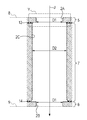
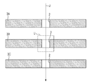
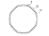
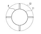
도 1a에 예시된 바와 같이, 본 발명에 따른 하전 입자 빔 렌즈는 3개의 전극(3A, 3B, 및 3C)을 포함한다. 3개의 전극 각각은 법선으로서 광축(J)을 갖고, 제1 표면 및 제1 표면의 반대편의 제2 표면을 포함하는 평판이다. 전극들은 서로 전기적으로 절연된다. 제1 표면은 통상적으로 전면이며, 제2 표면은 통상적으로 후면이다. 여기서, “전” 및 “후”라는 용어는 편의상 상대적 관계를 표시하기 위해서만 사용된다. 전극들(3A, 3B, 및 3C) 각각은 전극 패드(10)를 포함하며, 이를 통해 전극의 전위가 제어된다. 빔원(미도시)으로부터 방출되는 하전 입자가 하전 입자 빔은 화살표로 표시된 방향으로 광축(J)을 따라 통과한다. 광축(J) 방향의 전극 길이는 두께라고 지칭될 것이다.As illustrated in FIG. 1A, the charged particle beam lens according to the present invention comprises three
3개의 전극 각각은 소정의 두께를 갖는 3개의 영역을 포함하는데, 이들 영역은 제1 영역(5), 제2 영역(6), 제1 영역과 제2 영역 사이에 배치된 제3 영역(7)이다. 여기서, 전극의 두께가 광축(J) 방향의 전극 길이라고 가정된다. 도 1a에 예시된 바와 같이, 제1 영역(5)은 광축(J) 방향에 대해 빔원 측의 전극의 전체 표면을 포함하며, 소정의 두께를 갖는다. 마찬가지로, 제2 영역은 광축(J) 방향에 대해 빔원 측의 반대측에 있는 전극의 전체 표면을 포함하며, 소정의 두께를 갖는다. 제1 영역과 제2 영역 사이에 배치된 제3 영역은 전극의 나머지 영역으로서 소정의 두께를 갖는다.Each of the three electrodes includes three regions having a predetermined thickness, which regions are the
제1 영역(5), 제2 영역(6), 및 제3 영역(7)은 개구(2A), 개구(2B), 및 개구(2C)를 각각 포함한다. 도 1a에 예시된 바와 같이, 개구(2A, 2B, 및 2C)는 두께 방향으로 전극을 관통하여 연장되는 관통-홀들이다. 하전 입자 빔이 개구들(및 관통-홀)을 통과할 수 있다. 도 1b에 예시된 바와 같이, 개구(2A)는 원형이다. 마찬가지로, 개구 단면이 법선으로서 광축(J)을 갖는 평면을 따라 절취된 개구의 단면으로서 정의되는 경우, 개구(2B 및 2C)의 개구 단면은 개구(2A)의 원형과 동심인 원형이다. 개구(2C)의 개구 단면의 직경은 개구(2A 및 2B)의 개구 단면의 직경보다 더 크다. 그러므로, 도 1a에 예시된 바와 같이, 전극(3A, 3B, 및 3C) 각각에 형성된 관통-홀은 그 직경이 출입 시에 더 작아지도록 프로파일을 갖는다. 여기에서, 광축은 전자 빔이 통과하는 방향으로 연장된다.The
예를 들어, 전극(3A 및 3C)의 전위가 접지 전위로 유지되는 동안 전극(3B)에 음의 정전압을 인가함으로써 소위 단독(einzel) 정전 렌즈가 형성된다. 본 발명에서, “단독 정전 렌즈”라는 용어는 복수의(통상 3개의) 전극이 소정의 간격으로 배열되고, 최외각 전극들의 전위가 접지 전위로 유지되고, 양전위 또는 음전위가 다른 전극에 인가되는 정전 렌즈를 지칭한다. 3개의 전극이 사용되는 경우, 하전 입자 빔의 입사 측으로부터의 제1 전극 및 제3 전극이 접지 전위로 유지되고, 양전위 및 음전위가 제2 전극에 인가된다. 빔이 전극(3A, 3B, 및 3C)의 개구들을 순차적으로 통과하는 동안 하전 입자 빔이 렌즈 효과를 받는다. 동시에, 전극(3A와 3B) 사이 또는 전극(3B와 3C) 사이에 정전 인력이 생성된다.For example, a so-called einzel electrostatic lens is formed by applying a negative constant voltage to the
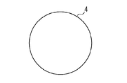
우선, 도 11a 내지 도 11f를 참조하면, 본 발명에 따른 하전 입자 빔 렌즈를 설명하는데 필요한 개구 단면의 대칭성의 정의가 설명된다. 정전 하전 입자 빔 렌즈의 렌즈 효과를 생성하는 정전기장이 개구 단면에 의해 형성된다. 특히, 비점 수차 및 고위 수차가 광축(J) 주위의 회전 비대칭성으로 인해 생성되기 때문에, 완벽한 원으로부터의 편차가 중요한 지표이다.First, referring to Figs. 11A to 11F, the definition of the symmetry of the opening cross section required for explaining the charged particle beam lens according to the present invention is explained. An electrostatic field is created by the aperture cross section that creates the lens effect of the electrostatically charged particle beam lens. In particular, since astigmatism and high order aberrations are generated due to rotational asymmetry around the optical axis J, deviation from a perfect circle is an important indicator.
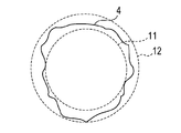
도 11a는 이상적으로 원형(완벽한 원)인 개구 단면(4)을 나타낸다. 여기에서, 개구 단면이 법선으로서 광축(J)을 갖는 평면 및 개구의 교차 부분인 폐곡선이다. 두께 방향을 따라 임의의 위치에 개구 단면이 정의될 수 있다. 도 11b는 타원형인 개구 단면(4)을 나타낸다. 다음의 지표는 본 발명에 따른 전하 빔 렌즈 빔의 비점 수차 및 고위 수차들에 영향을 미치는 형상 오차의 측정치로서 정의된다. 도 11b에 예시된 타원형의 개구 단면(4)은 동심 원들과 접촉하기 위해 2개의 동심 원 사이에 배치된다. 내측원은 내접원(11)이라고 지칭될 것이고, 외측원은 외접원(12)이라고 지칭될 것이다. 상이한 중심 주변에 그려질 수 있는 이러한 동심 원들의 여러 조합 중에, 반지름의 차이가 가장 작은 내접원과 외접원 쌍이 선택된다. 진원도는 이러한 방식으로 선택되는 내접원과 외접원의 반경 차이의 절반으로서 정의된다. 도 11a에 예시된 완벽한 원형인 개구 단면(4)의 경우, 그 이유는 외접원 및 내접원이 서로 일치하기 때문에 진원도가 0이다.11a shows an
도 11c에 예시된 바와 같이, 진원도는 타원형 이외의 임의의 형상에 대해 유사한 방식으로 정의된다.As illustrated in FIG. 11C, roundness is defined in a similar manner for any shape other than elliptical.
설계 측면에서 이상적인 형상은 원형이 아니라 도 11d에 예시된 바와 같이 다각형 형상일 수 있다(다음의 설명에서 예시로서 8각형이 사용됨). 이 경우, 진원도, 대표 반경(이하 설명됨), 및 대표 직경(이하 설명됨)은 다음의 방법으로 정의된다. 즉, 개구의 크기 및 이상적인 8각형으로부터의 대칭성의 편차는 진원도, 대표 반경, 및 대표 직경에 의해 비교될 수 있다. 도 11d는 이상적인 8각형의 외접원(12) 및 내접원(11)을 나타낸다. 8각형의 경우, 진원도는 이상적인 상태에서도 0 이상이다. 도 11e는 형상 오차를 갖고 정8각형으로부터 이탈된 8각형의 외접원(12) 및 내접원(11)을 나타낸다. 그러므로, 도 11e의 경우의 진원도는 정8각형의 경우인 도 11d의 진원도보다 크다.In design terms, the ideal shape may be a polygonal shape as illustrated in FIG. 11D rather than circular (an octagon is used as an example in the following description). In this case, roundness, representative radius (described below), and representative diameter (described below) are defined in the following manner. That is, the size of the aperture and the deviation of symmetry from the ideal octagon can be compared by roundness, representative radius, and representative diameter. 11D shows an ideal octagonal circumscribed
진원도는 단면 형상을 실제 측정함으로써 정의될 수 있다. 선택 형상은 둘레를 가능한 한 충분히 많은 개수의 분할 영역으로 나누고, 영상 처리를 통해 외접원(12) 및 내접원(11)을 획득함으로써 계산될 수 있다.Roundness can be defined by actually measuring the cross-sectional shape. The selection shape can be calculated by dividing the circumference into as many partitions as possible and obtaining the circumscribed
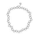
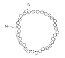
대표 직경 및 대표 반경은 다음과 같이 정의된다. 도 13a 내지 도 13c는 도 11c의 개구 단면(4)의 대표 직경을 정의하는 단계들을 나타낸다. 도 13a의 개구 단면(4)의 윤곽선은 도 13b에 예시된 충분히 작은 간격으로 서로 이격된 이산 측정 지점 세트(13)로서 측정된다. 그 간격은 개구 단면(4)의 요철의 대표 주기의 절반보다 작을 수 있다. 이러한 방법으로 측정된 측정 지점(13)을 사용함으로써, 대표 원(14)이 도 13c에 예시된 바와 같이 유일하게 결정된다. 원의 방정식에 기하학적으로 맞도록 측정 지점들(13)을 사용함으로써 회귀 분석이 수행된다. 회귀 분석은 최우법(maximum likelihood method)을 사용함으로써 수행될 수 있다. 측정 지점(13)이 충분히 작은 간격으로 측정되면, 최소자승법이 사용될 수 있다. 대표 직경 및 대표 반경이 이러한 방식으로 결정되는 대표 원(14)의 직경 및 반경으로서 정의된다. 대표 원의 대표 직경 및 대표 반경이 광축에 또는 광축 부근의 전위 분포를 판단하는 대표 형상으로서 중요한데, 그 이유는 하전 입자 빔이 개구의 중심으로 통과하기 때문이다.Representative diameters and representative radii are defined as follows. 13a-c show the steps of defining the representative diameter of the
도 11f는 대부분이 원형이고 나머지가 돌출 형상인 개구 단면(4)을 예시한다. 이 경우에도, 대표 직경 및 대표 반경은 전술한 방법을 사용함으로써 광축의 근처의 전기장에 기여하는 대표 형상인 대표 원을 결정함으로써 판단될 수 있다. 이러한 원이 획득되는 경우, 외접원(12) 및 내접원(11)이 기하학적 맞춤을 수행함으로써 획득되었던 원과 동심인 원들을 그려서 정의된다.11F illustrates the
전술된 정의에 기반하여 진원도, 대표 반경, 및 대표 직경이 임의의 개구 단면에 대해 정의된다. 이하, 개구 단면의 이상적인 형상으로서 원이 사용된다. 그러나, 이상적인 형상은 8각형 또는 임의의 다른 곡선일 수 있다. 또한, 이러한 경우, 진원도, 대표 반경, 및 대표 직경은 본 발명에서 정의 및 사용될 수 있다.Roundness, representative radius, and representative diameter are defined for any opening cross section based on the above definition. Hereinafter, a circle is used as an ideal shape of an opening cross section. However, the ideal shape may be an octagon or any other curve. Also in this case, roundness, representative radius, and representative diameter can be defined and used in the present invention.
다음으로, 수차에 대한 개구 단면의 진원도의 효과가 설명될 것이다.Next, the effect of the roundness of the opening cross section on the aberration will be explained.
우선, 도 6을 참조하면, 정전 하전 입자 빔 렌즈가 하전 입자 빔을 수렴하는 메커니즘이 설명될 것이다. 도 6에서, R축은 렌즈의 반경 방향으로 연장되고, J축은 광축 방향으로 연장되고, “O”는 원점을 지칭한다. 도 6은 J-축에 평행한 평면을 따라 절취된 단독 렌즈의 단면도이다. 단독 렌즈는 3개의 전극(3A, 3B, 및 3C)을 포함한다. 전극들(3A 및 3C)의 전위는 접지 전위로 유지되고, 음전위가 전극(3B)에 인가된다. 하전 입자 빔이 음 전하를 갖는다. 3개의 전극(3A, 3B, 및 3C)은 각각이 법선으로서 광축(J)을 갖는 평판이다.First, referring to FIG. 6, the mechanism by which the electrostatic charged particle beam lens converges the charged particle beam will be described. In Fig. 6, the R axis extends in the radial direction of the lens, the J axis extends in the optical axis direction, and “O” refers to the origin. 6 is a cross-sectional view of a single lens cut along a plane parallel to the J-axis. The single lens comprises three
이 상태에서 전속선(electric flux line)들이 실선 화살표 H에 의해 예시된다. X 방향으로의 3개의 전극(3A, 3B, 및 3C)의 중간면들 및 3개의 전극 사이의 공간들의 중간면들이 파선으로 예시되어 있다. J축을 따른 파선들 사이의 간격들은 구간 I, 구간 II, 구간 III, 및 구간 IV라고 지칭될 것이다. 단독 렌즈의 주요 렌즈 효과의 설명의 편의를 위해, 구간 I의 원점 O 측에서의 간격 및 원점 O의 반대측의 구간 IV의 일측의 구간에 전위가 제공되지 않는다.Electric flux lines in this state are illustrated by the solid arrow H. Intermediate planes of the three
R > 0인 영역에서 구간 I, 구간 II, 구간 III, 및 구간 IV의 전기장 방향은 화살표(f1, f2, f3, 및 f4)에 의해 각각 표시된다. 구간 I, 구간 II, 구간 III, 및 구간 IV의 전기장 방향은 각각 음, 양, 양, 및 음이다. 그러므로, 영상 높이 r0를 통과하는 하전 입자 빔의 경로는 화살표 E로 표시되는 바와 같다. 즉, 하전 입자 빔은 구간 I에서 발산되고, 구간 II에서 수렴되고, 구간 III에서 수렴되고, 구간 IV에서 발산된다. 이는 X축 방향으로 배열된 오목 렌즈, 볼록 렌즈, 볼록 렌즈, 및 오목 렌즈와 광학적으로 등가이다.In the region where R> 0, the electric field directions of the sections I, II, III and IV are indicated by arrows f1, f2, f3 and f4, respectively. The electric field directions of sections I, II, III and IV are negative, positive, positive and negative, respectively. Therefore, the path of the charged particle beam through the image height r0 is as indicated by arrow E. That is, the charged particle beam diverges in section I, converges in section II, converges in section III, and diverges in section IV. This is optically equivalent to the concave lens, the convex lens, the convex lens, and the concave lens arranged in the X-axis direction.
하전 입자 빔은 다음의 2가지 이유로 수렴된다. 첫번째 이유는 더 강한 힘이 더 큰 영상 높이에서 하전 입자 빔에 인가되기 때문에 구간 II 및 구간 III에서의 수렴의 효과는 구간 I 및 구간 IV에서의 발산의 효과보다 더 크다. 두번째 이유는 하전 입자 빔이 구간 I에서보다 더 오랜 시간 동안 구간 II에서 이동하며, 구간 IV에서보다 더 오랜 시간 동안 구간 III에서 이동한다는 점이다. 모멘텀의 변화가 임펄스와 동일하기 때문에, 전자 빔이 이동하는데 오랜 시간이 걸리는 간격으로 전자 빔에서 더 큰 효과가 생긴다.The charged particle beam converges for two reasons: The first reason is that the effect of convergence in sections II and III is greater than the effect of divergence in sections I and IV because stronger forces are applied to the charged particle beam at larger image heights. The second reason is that the charged particle beam travels in section II for a longer time than in section I and travels in section III for a longer time than in section IV. Since the change in momentum is equal to the impulse, there is a greater effect on the electron beam at intervals that take longer to move the electron beam.
수렴 효과는 전술한 이유 때문에 생성된다. 하전 입자 빔은 양전위가 전극(3B)에 인가되는 경우 유사한 방식으로 수렴된다. 양 전하를 갖는 하전 입자 빔이 더 수렴된다. 수렴 효과는 전극(3B)의 양/음 전위 및 하전 입자 빔의 양/음 전하의 임의의 조합에 대해 생긴다. 구간 I 내지 구간 IV에서 전기장을 형성하는 개구(2)의 형상 오차로 인해 수렴 필드의 대칭성이 파괴되면, 정전 렌즈는 비점 수차와 같은 고위 수차를 갖는다. 그러므로, 개구의 형상이 정확하게 형성되는 것이 필요한데, 그 이유는 정전 하전 입자 빔의 수차가 전극에 형성된 개구의 형상 오차에 의해 민감하게 영향을 받기 때문이다.The convergence effect is created for the reasons mentioned above. The charged particle beam converges in a similar manner when a positive potential is applied to the
개구가 형성될 전극이 두꺼울수록, 개구의 형상 오차를 감소시키는 것은 더 어렵다. 전극의 두께가 큰 경우, 전극의 내부를 관통하여 전면 및 후면에 있는 개구의 형상 오차를 제어하는 것은 어렵다. 그 결과, 요구되는 정밀도가 높아지면, 가공 비용이 증가하거나 제조가 어려워질 수 있다. 가공 난이도를 감소시키기 위해, 더 얇은 전극이 사용될 수 있다. 그러나, 단순히 전극의 두께가 감소되면, 전극에 인가된 전압에 의해 생성되는 정전 인력으로 인해 전극이 변형될 수 있다. 정전 렌즈의 수차를 감소시키기 위해, 렌즈의 초점 거리를 감소시킴으로써 구면 수차를 감소시는 것 또한 필요하다. 그러나, 이 경우, 전극 사이에 강한 자기장이 생성되며, 이로써 정전 인력으로 인한 전극의 변형이 중대한 문제점을 일으킨다. 전극의 변형이 일어나면, 전극 사이의 거리 오차가 발생하며, 개구가 광축(J)에 대해 기울어질 수 있으며, 이로써 하전 입자 빔의 렌즈 효과에 영향을 미치는 개구 형상의 대칭성이 후술되는 바와 같이 파괴될 수 있다. 그 결과, 구면 수차가 감소됨에도 불구하고, 고위 수차들이 증가하거나, 하나의 전극에 복수의 개구를 갖는 렌즈 어레이의 경우 개별 렌즈의 초점 거리의 변동이 일어날 수 있다.The thicker the electrode on which the opening is to be formed, the more difficult it is to reduce the shape error of the opening. When the thickness of the electrode is large, it is difficult to control the shape error of the openings in the front and back through the inside of the electrode. As a result, the higher the required precision, the higher the processing cost or the more difficult the manufacture may be. Thinner electrodes may be used to reduce processing difficulty. However, if the thickness of the electrode is simply reduced, the electrode may deform due to the electrostatic attraction generated by the voltage applied to the electrode. In order to reduce the aberration of the electrostatic lens, it is also necessary to reduce the spherical aberration by reducing the focal length of the lens. In this case, however, a strong magnetic field is generated between the electrodes, which causes a serious problem of deformation of the electrode due to electrostatic attraction. If the deformation of the electrode occurs, a distance error between the electrodes occurs, and the opening can be inclined with respect to the optical axis J, whereby the symmetry of the opening shape which affects the lens effect of the charged particle beam will be destroyed as described below. Can be. As a result, although spherical aberration is reduced, high order aberrations may increase, or in the case of a lens array having a plurality of openings in one electrode, variations in the focal length of individual lenses may occur.
그러므로, 개구가 큰 두께로 연장되는 부위의 개구 단면의 진원도의 기여율이 감소될 수 있으며, 관통-홀을 형성하는 난이도를 증가시키지 않고 렌즈의 수차가 감소될 수 있다.Therefore, the contribution of the roundness of the opening cross section of the portion where the opening extends to a large thickness can be reduced, and the aberration of the lens can be reduced without increasing the difficulty of forming the through-hole.
본 발명에 따른 하전 입자 빔 렌즈에서, 하전 입자 렌즈가 통과하는 개구는 제1 영역의 개구(2A), 제2 영역의 개구(2B), 및 제3 영역의 개구(2C)로 분할되며, 개구(2C)의 대표 직경은 개구(2A) 및 개구(2B)의 대표 직경보다 크다. 개구의 이러한 분할을 이용하면, 수차에 대한 개구(2C)의 기여를 감소시키고, 이 부위의 개구 단면이 좋지 않으면 렌즈의 수차에 대한 이러한 부위의 영향이 감소될 수 있다.In the charged particle beam lens according to the present invention, the opening through which the charged particle lens passes is divided into an
다음으로, 도 2a, 도 2b, 및 도 4를 참조하면, 전체 비점 수차에 대한 제3 영역의 개구(2C)의 진원도의 영향이 본 발명에 따른 대표 직경 사이의 관계를 사용함으로써 감소될 수 있다는 사실이 설명될 것이다.2A, 2B, and 4, the effect of the roundness of the
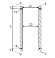
도 2a는 도 1a의 파선 M에 의해 둘러싸인 본 발명에 따른 전극(3B)의 부위의 확대 단면도이다. 도 2a에 예시된 바와 같이, 제1 영역(5)의 개구(2A), 제2 영역의 개구(2B), 및 제3 영역의 개구(2C)는 각각 대표 지름 D1, D1 및 D2를 갖는다. 여기에서, 자유 표면 측의 제1 영역(5)의 표면은 전극(3B)의 제1 표면이고, 자유 표면 측의 제2 영역(6)의 표면은 제2 표면이다. 즉, 전극(3B)은 제1 표면 및 제1 표면의 반대편인 제2 표면을 갖는다. 전술한 바와 같이, D1 < D2이다. 두께는 각각 t, t, 및 t'이다. 전극(3B)은 제1 계면(13) 및 제2 계면(14)을 통해 접합된 구조를 갖는다. 제1 영역(5)은 법선으로서 광축(J)을 갖는 전극(2B)의 최외각 표면에 대응하는 제1 표면(8)을 포함한다. 제2 영역은 제1 표면(8)의 반대 측에서 법선으로서 광축(J)을 갖는 전극(2B)의 최외각 표면에 대응하는 제2 표면(9)을 포함한다. 도 2b는 대표 직경 D1 및 D2가 동일한 경우로서 종래 기술의 경우를 예시한다. 도면에 예시된 바와 같이, 도 2b는 대표 직경 D1 및 D2 사이의 관계를 제외하고 도 2a와 동일한 구조를 예시한다.FIG. 2A is an enlarged cross-sectional view of a portion of the
도 4는 도 2a 및 도 2b의 경우에서 렌즈의 비점 수차에서의 개구들(2A 및 2B)의 수차의 합산의 비율(기여율)을 예시한다. 수평축은 개구들(2A 및 2B)의 직경 D1과 두께 t의 비를 표현한다. 속이 찬(solid) 원들은 직경 D1 및 D2가 동일한 경우를 표현한다.4 illustrates the ratio (contribution rate) of the sum of the aberrations of the
직경 D1 및 D2이 동일한 경우, 개구들(2A 및 2B)이 두께 t는 직경 D1의 1/8이고, 개구들(2A 및 2B)의 수차들의 합이 전체 수차의 80%를 차지할 수 있다. 개구들(2A 및 2B) 사이에 작은 차이가 존재하기 때문에, 개구들(2A, 2B, 및 2C)의 기여율은 각각 44%, 36%, 및 20%이다.When the diameters D1 and D2 are the same, the thicknesses t of
도 4의 속이 빈(open) 원들은 직경 D1이 직경 D2의 0.8배인 본 발명의 경우를 표현한다. 직경 D1이 직경 D2의 0.8배인 경우, 직경 D1 및 D2가 동일한 경우에 비해, 두께 t가 작은 경우에도 개구들(2A 및 2B)의 기여율이 높다. 두께 t가 직경 D1의 1/8인 경우, 기여율은 약 94%이다. 두께 t가 직경 D1의 1/5인 경우, 기여율은 96%이다. 이에 따라, 특히, D1 < D2인 영역에서, 개구(2A 및 2B)의 기여율은 더 증가될 수 있다.The open circles in FIG. 4 represent the case of the present invention in which the diameter D1 is 0.8 times the diameter D2. When the diameter D1 is 0.8 times the diameter D2, the contribution ratio of the
기여율 사이의 관계는 개구(2C)의 두께 t'가 변하는 경우에도 변하지 않는다. 그러므로, 개구(2C)의 두께를 증가시킴으로써, 기여율 사이의 관계를 유지하면서 전극 전체의 두께는 증가될 수 있다. 이 경우, 수차에 대한 개구들(2A 및 2B)의 기여율이 높기 때문에, 렌즈의 전체의 수차에 대한 영향은 개구(2C)가 큰 제조 오차를 갖는 경우에도 감소될 수 있다.The relationship between the contribution ratios does not change even when the thickness t 'of the
이후, 개구들(2A 및 2B)과 같이 수차에 대한 기여율이 표면 근처 위치의 개구 단면에 의해 상당한 영향을 받는 메커니즘, 및 개구가 형성되는 평판의 두께와 개구 단면의 진원도 사이의 관계가 순서대로 설명될 것이다.Then, the mechanism in which the contribution to aberration is significantly influenced by the opening cross section at the position near the surface, such as the
도 7을 참조하면, 수차에 대한 개구의 형상의 기여율은 위치가 개구들(2A 및 2B)에서의 위치들과 같은 제1 영역 및 제2 영역의 표면 근처의 위치로부터 관통-홀에서 더 깊게 이동함에 따라 감소한다. 도 7은 도 6의 파선 Z에 의해 둘러싸인 부위의 확대 단면도이다. 곡선 K, L, 및 M은 전극(3B)의 개구(2)의 표면 근처의 공간의 등전위선(equipotential line)들을 표현한다. 곡선 H는 개구(2)의 최외각 표면에 대응하는 전속선들을 표현한다. 도 7에 예시된 바와 같이, 곡선 K, L, 및 M은 전속선 H의 외부 영역의 전극(3B)의 표면(즉, 개구(2)가 형성되지 않은 측면)에 실질적으로 평행하다. 그러므로, 이 영역에서의 전속선들은 전극의 법선에 실질적으로 평행이다. 그러므로, 렌즈 효과를 생성하는 R 방향으로의 전기장에 대한 이 영역에서의 전극의 형상의 영향(도 6의 f1, f2, f3, 및 f4 참조)은 무시할 수 있을 정도로 작다.Referring to FIG. 7, the contribution of the shape of the opening to the aberration moves more deeply in the through-hole from the position near the surface of the first region and the second region, such as the positions in the
한편, 등전위선 K, L, 및 M은 전속선 H의 내부 영역(즉, 개구(2)가 형성된 측면)에서 개구(2)의 내부를 향해 구부러진다. 그러므로, 전속선 H 및 전속선 H 내부의 전속선들은 R 방향으로 전기장을 형성하는데, 이는 도 6을 참조하여 설명되는 바와 같이 렌즈 효과를 생성한다. 3차원적으로, 하전 입자 빔이 도 6에 예시된 전기장에 의해 R 방향으로 영향을 받으며, 법선으로서 광축(J)을 갖는 평면에서 광축(J)의 중심 주변의 모든 원주 방향으로 렌즈 효과를 생성한다. 광축(J) 주변의 원주 방향의 전속선 H 및 전속선 H 내부의 전속선의 대칭성(즉, 원형의 진원도)은 법선으로서 광축(J)을 갖는 평면을 따라 절취된 개구(2)의 단면의 형상의 대칭성에 의해 영향을 받는다. 등전위선 K, L, 및 M 사이의 거리는 개구(2)의 광축(J)을 향해 증가한다. 전속선 밀도는 전속선 H로부터의 내부 방향, 및 두께 방향의 더 깊은 방향으로 감소한다. 그러므로, 전극의 최외각 표면에서의 개구(2)의 단면 형상은 하전 입자 빔의 수렴에 가장 크게 영향을 미치고, 이 영향은 두께 방향으로의 깊이가 증가할수록 감소한다.On the other hand, the equipotential lines K, L, and M are bent toward the inside of the
여기에서, 도 6의 구간 II에서의 전기장 방향 f2가 상세히 설명되었다. 동일한 이유로 인해, 구간 I, III, 및 IV에서의 전기장 방향 f1, f3, 및 f4 각각에 관해, 전극의 최외각 표면의 개구(2)의 단면 형상은 하전 입자 빔의 수렴에 가장 크게 영향을 미친다. 그러므로, 그 영향은 최외각 표면으로부터의 거리가 증가함에 따라 감소한다.Here, the electric field direction f2 in the section II of FIG. 6 has been described in detail. For the same reason, for each of the electric field directions f1, f3, and f4 in the sections I, III, and IV, the cross-sectional shape of the
개구의 깊이가 증가하는 경우라도, 표면 근처의 개구 단면의 기여율은 변하지 않는다. 즉, 수차에 대한 개구(2A 및 2B)의 기여율을 변경시키지 않고 개구(2C)의 두께가 증가될 수 있다. 개구(2C)의 개구 단면의 진원도가 본 발명의 대표 직경 사이의 관계 D1 < D2으로 인해 수차에 대해 작은 기여율만을 갖기 때문에, 수차의 증가를 억제하면서 전체 전극의 두께 및 강도가 증가될 수 있다.Even when the depth of the opening increases, the contribution ratio of the opening cross section near the surface does not change. That is, the thickness of the opening 2C can be increased without changing the contribution ratio of the
도 8 및 도 9를 참조하면, 평판에서의 관통-홀을 형성하는 프로세스와 진원도 사이의 관계가 설명될 것이다. 도 8은 전극들(3A, 3B, 및 3C)로서 단결정 실리콘의 평판을 포함하는 하전 입자 빔 렌즈의 단면도이다. 도 1a의 경우에서와 같이, 각각의 전극은 하전 입자 빔이 통과하는 개구(2)를 갖는다. 도 9는 도 8의 파선 U에 의해 둘러싸인 부위의 확대 단면도이다.Referring to Figures 8 and 9, the relationship between the roundness and the process of forming the through-holes in the plate will be described. 8 is a cross-sectional view of a charged particle beam lens comprising a flat plate of single crystal silicon as the
도 9는 개구가 화살표 N 방향으로 기판을 통해 연장되도록 단결정 실리콘의 딥 드라이 에칭(deep dry etching)을 수행함으로써 형성되는 단면 형상을 예시한다. 딥 드라이 에칭 프로세스에서, 에칭 가스 및 보호 가스를 교대로 공급하면서 에칭이 수행된다. 그러므로, 도 9에 예시된 바와 같이, 스캘럽(scallop)이라고 지칭되는 소형 요철이 측면에 형성된다. 에칭 프로세스로서, 에칭 가스와 보호 가스의 공급 및 배출 및 화학 반응으로 인한 열과 같은 요철에 영향을 미치는 오차 요인들이 증가한다. 그러므로, 요철의 깊이 및 피치(pitch)가 위치에 따라 변하며, 이로써 진원도가 더 악화될 수 있다. 더구나, 개구가 기판을 관통하여 연장되기 직전에 개구가 형성되고 있는 방향으로의 계면의 존재로 인해 에칭 가스의 경로가 휘어지며, 이로써 “파선 S로 둘러싸인 영역에 의해 도시된 바와 같이 개구가 넓어지는 “노칭(notching)”이라고 지칭되는 현상이 일어난다고 알려져 있다. 이 효과로 인해, 이러한 개구의 진원도가 화살표 N 방향으로 더 악화된다. 그러므로, 파선 S에 의해 둘러싸인 영역의 진원도가 가장 악화되어 있다. 개구에서의 에칭 깊이가 깊어질수록, 에칭 개시면(화살표 N의 뒷부분 근처의 표면)에서의 에칭 마스크의 에지 부위(미도시)에서 사이드 에칭(side etching)이 더 자주 일어나며, 이로써 에칭 마스크의 개구 형상이 변형된다. 그러므로, 진원도가 악화된다. 전술한 바와 같이, 평판에서의 개구를 형성할 때, 평판의 두께가 커질수록 진원도가 악화된다.9 illustrates a cross-sectional shape formed by performing deep dry etching of single crystal silicon such that the opening extends through the substrate in the direction of arrow N. FIG. In the deep dry etching process, etching is performed while alternately supplying an etching gas and a protective gas. Therefore, as illustrated in Fig. 9, small irregularities called scallops are formed on the side. As an etching process, error factors that affect the unevenness such as heat due to supply and discharge of etching gas and protective gas and chemical reactions are increased. Therefore, the depth and pitch of the unevenness change with the position, whereby the roundness may be worsened. Furthermore, the presence of the interface in the direction in which the opening is being formed immediately before the opening extends through the substrate causes the path of the etching gas to bend, thereby expanding the opening as shown by the area enclosed by the broken line S. A phenomenon called "notching" is known to occur. Due to this effect, the roundness of this opening is further worsened in the arrow N direction. Therefore, the roundness of the area | region enclosed by the broken line S is the worst. The deeper the etch depth at the opening, the more often side etching occurs at the edge region (not shown) of the etching mask at the etching start surface (surface near the back of arrow N), thereby opening the etching mask. The shape is deformed. Therefore, roundness deteriorates. As described above, when forming the opening in the flat plate, the larger the thickness of the flat plate, the worse the roundness.
본 발명을 이용하면, 개구(2C)의 두께가 증가되는 경우에도, 수차에 대한 이 부위에서의 개구 단면의 기여율이 낮다. 그러므로, 높은 진원도를 갖는 개구를 형성하는 정밀도가 두께 증가로 인해 개선될 수 없는 경우에도 렌즈의 수차의 증가가 억제될 수 있다.With the present invention, even when the thickness of the opening 2C is increased, the contribution ratio of the opening cross section at this site to aberration is low. Therefore, even if the accuracy of forming the opening with high roundness cannot be improved due to the increase in thickness, the increase in the aberration of the lens can be suppressed.
다음으로, 두께 방향으로의 제1 영역 내지 제3 영역의 개구 단면의 진원도가 설명될 것이다. 도 14는 도 2a의 제3 영역(7)에서 도 9에 도시된 바와 같은 실리콘의 딥 드라이 에칭을 수행함으로써 형성되는 관통-홀을 예시한다. 도 14는 제3 영역(7)만을 예시한다. 도 14에서의 화살표 T1 내지 화살표 T5에 의해 표시되는 바와 같이, 개구 단면들은 깊이 방향을 따라 임의의 위치에서 정의될 수 있다. 전술한 대표 직경 및 진원도는 이들 개구 단면 각각에 대해 정의될 수 있다. 여기에서, 제3 영역(7)의 대표 직경 및 진원도는 개구의 깊이 방향으로 임의의 위치에서 이러한 방식으로 정의될 수 있다. 최외각 표면(자유 표면이라고도 지칭됨) 이외의 영역의 일부의 대표 직경 및 진원도는 개구를 도금 등을 이용하여 일시적으로 매립하고, 연마한 후, 개구를 관찰함으로써 측정될 수 있다. 대안으로서, 이러한 직접적인 측정을 수행하는 대신, 최외각 표면의 측정이 대표 값으로서 사용될 수 있다. 최외각 표면 이외에 제1 영역 내지 제3 영역의 부분들은 수차에 더 적게 기여하는 부분들이다. 그러므로, 최외각 표면들에 비해, 동일한 자릿수에서의 이들 부분의 대표 직경 및 진원도의 변화가 수차에 더 적게 영향을 미친다. 그러므로, 두께 방향으로의 개구의 여러 섹션에서의 대표 직경 및 진원도의 측정값들이 상이한 자릿수를 갖는 이상점(outlier)들을 포함하는 값들의 분포를 갖지 않으면, 최외측 표면들(즉, 도 14에서 위치 T1 및 T5)에서의 대표 직경 및 진원도의 평균이 대표 값으로서 사용될 수 있다.Next, the roundness of the opening cross section of the first to third regions in the thickness direction will be described. FIG. 14 illustrates a through-hole formed by performing a deep dry etch of silicon as shown in FIG. 9 in the
다음으로, 도 3을 참조하면, 더 알맞은 직경 범위 D1 < D2가 설명될 것이다. 도 3a는 도 2a의 파선 Y에 의해 둘러싸인 영역의 확대 단면도이다. 도 1a에 예시된 전극들(3A 및 3C)은 접지 전위로 유지되고, 음전위가 전극(3B)에 인가된다. 그러므로, 제1 영역(5)의 상부 표면에 정전 인력이 생성된다. 이하, 이러한 정전 인력은 근사치로서 분포 하중(distributed load) w로 간주될 것이다.Next, referring to FIG. 3, a more suitable diameter range D1 <D2 will be described. 3A is an enlarged cross-sectional view of a region surrounded by the broken line Y in FIG. 2A. The
D1 < D2인 경우, 도 3a에 예시된 바와 같이 제1 영역(5)은 제3 영역을 향해 고리 형상으로 돌출된 돌출부를 갖는다. 돌출부는 정전 인력을 받으면 분포 하중 w 방향으로 변형된다. (단면도인 도 3a의 선분 PQ에 의해 표현된) 돌출부의 끝면(end face)의 분포 하중 방향 변형 y가 다음의 수학식으로 표현될 수 있다.When D1 <D2, as illustrated in FIG. 3A, the


(E는 영률(Young's modulus)이고, v는 푸아송 비(Poisson's ratio)임)(E is Young's modulus, v is Poisson's ratio)
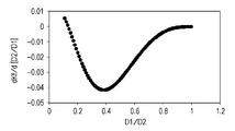
수학식 1의 계수 Kf는 직경 D1과 직경 D2의 비의 함수이고, 고리 형상의 돌출부의 강도에서 직경 D1 및 D2의 형상 인자의 계수이다. 계수 Kf는 위치 변화 y의 비례 계수이다. 그러므로, 계수 Kf가 클수록, 강도가 낮아진다.The coefficient K f in equation (1) is a function of the ratio of the diameter D1 to the diameter D2, and is a coefficient of the shape factor of the diameters D1 and D2 in the strength of the annular protrusion. The coefficient K f is a proportional coefficient of the position change y. Therefore, the larger the coefficient K f , the lower the strength.
도 3b는 직경 D1 및 D2의 비의 함수로서 계수 Kf를 나타내다. D1/D2가 1에 접근함에 따라(즉, 돌출부가 더 작아짐에 따라), 강도가 증가한다. 도 3c는 D1/D2에 관해 계수 Kf의 도함수를 나타낸다. 계수 Kf의 미분 계수는 D1/D2 = 0.4 근처의 최소값을 갖는다.3b shows the coefficient K f as a function of the ratio of diameters D1 and D2. As D1 / D2 approaches 1 (ie, as the protrusions become smaller), the strength increases. 3C shows the derivative of the coefficient Kf with respect to D1 / D2. The derivative of the coefficient K f has a minimum value near D1 / D2 = 0.4.
미분 계수 Kf의 최소 지점 근처에서는 D1/D2의 변화에 대한 계수 변화의 비가 최대이다. 즉, 가공 오차로 인한 D1/D2가 변하면, 강도가 크게 변한다. 그러므로, 돌출부의 위치 변화 y가 크게 변한다. 이와 같이 가공 오차로 인해 위치 변화가 달라지면, 개구(2A)의 진원도가 달라질 수 있으며, 또한 유효 직경 D1이 변형에 따라 달라질 수 있다. 복수의 개수를 갖는 전극을 포함하는 렌즈 어레이의 경우, 개구들의 변형 사이의 차이는 더 커질 수 있다.Near the minimum point of the derivative coefficient K f , the ratio of the coefficient change to the change of D1 / D2 is maximum. That is, when D1 / D2 changes due to a machining error, the intensity changes significantly. Therefore, the positional change y of the protrusion largely changes. As such, when the position change is changed due to the machining error, the roundness of the
그러므로, D1/D2는 0.4보다 크고, 1.0보다 작을 수 있다. 이 범위에서, 계수 Kf 및 계수 Kf의 미분 계수의 절대값은 그 범위에서 작으며, 이로써 돌출부의 변형 및 개구의 가공 오차로 인한 변형의 변동 모두가 감소될 수 있다.Therefore, D1 / D2 may be greater than 0.4 and less than 1.0. In this range, the absolute value of the differential coefficients of the coefficient K f and the coefficient K f is small in that range, whereby both the deformation of the protrusion and the variation of the deformation due to the machining error of the opening can be reduced.
D1/D2가 0.8 이상이고 1.0 미만이면, 변형 및 그 변형의 변동은 더 감소될 수 있다. 특히, D1/D2가 0.8 이상이고 1.0 미만인 범위에서, D1/D2 = 0.8는 수차를 최소로 만들 수 있는 값이다.If D1 / D2 is greater than 0.8 and less than 1.0, the strain and variations in that strain can be further reduced. In particular, in the range where D1 / D2 is greater than 0.8 and less than 1.0, D1 / D2 = 0.8 is a value that can minimize aberration.
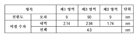
다음으로, 본 실시예의 물질 및 치수들의 특정 예들이 설명될 것이다. 전극들(3A, 3B, 및 3C) 각각의 제1 영역, 제2 영역, 및 제3 영역은 단결정 실리콘으로부터 만들어진다. 제1 영역, 제2 영역, 및 제3 영역의 두께는 각각 6마이크로미터, 6마이크로미터, 및 90마이크로미터이다. 개구들(2A 및 2B)의 직경 D1은 30마이크로미터이고, 개구(2C)의 직경(D2)은 36마이크로미터이다. 전극 패드(10)는 실리콘에 대한 접착력이 우수하고, 도전성이 높고, 내산화성이 높은 금속막으로 만들어진다. 예를 들어, 티타늄, 백금, 및 금으로 만들어진 다층막이 사용될 수 있다. 계면(13 및 14)에 실리콘 산화막이 형성된다. 전극들(3A, 3B, 및 3C)의 제1 표면(8)과 제2 표면(9) 및 개구들(2A, 2B, 및 2C)의 내벽면(inner wall)이 금속막에 의해 덮힐 수 있다. 이 경우, 산화에 대한 내성이 있는 백금과 같은 금속 또는 도전성을 갖는 몰리브덴 산화물이 사용될 수 있다. 전극(3A, 3B, 및 3C)은 서로 400마이크로미터의 거리만큼 서로 이격되고, 광축 J 및 법선을 갖는 평면에 평행하도록 배치된다. 전극들은 서로 전기적으로 절연된다. 전지 전위가 전극(3A 및 3C)에 인가되고, -3.7KV의 전위가 전극(3B)에 인가되며, 이로써 전극들이 단독 렌즈 역할을 한다. 도 5는 전자 빔이 하전 입자 빔으로서 사용되고 가속 전압이 5keV인 경우 본 실시예에 따른 전극(3B)의 비점 수차를 도시한 표이다. 개구들(2A 및 2B)의 진원도는 9nm이고, 개구(2C)의 진원도는 90nm이다. 표에 예시된 바와 같이, 비점수차의 내역은 2.14nm, 2.94nm, 및 1.74nm이다. 개구(2C)의 진원도가 개구(2A 및 2B)의 10배임에도 불구하고, 전제 전극(3B)의 비점 수차는 4.0nm이다(비점 수차의 값은 모두 가우시안 분포의 1/e 반경으로서 표현됨). 이는 개구들(2A, 2B, 및 2C)의 직격이 모두 30마이크로미터인 경우의 비점 수차에 대응하고, 100마이크로미터의 전체 두께에 걸친 단면 형상의 진원도는 9nm이다.Next, specific examples of materials and dimensions of the present embodiment will be described. The first, second, and third regions of each of the
(9nm의 진원도에 대응하는) 높은 진원도가 요구되는 개구의 부위들은 6마이크로미터의 두께의 박판으로 형성될 수 있다. 그러므로, 가공의 난이도가 감소될 수 있으며, 9nm 정도의 진원도의 오차를 갖는 원형 개구가 개구를 따라 형성될 수 있다. 개구(2C)의 영역에 90마이크로미터의 두께를 갖는 관통-홀을 형성하는 것이 필요함에도 불구하고, 이 부위의 진원도가 10배 악화될 수 있기 때문에 가공의 난이도가 증가되지 않는다.Portions of the opening where high roundness is required (corresponding to roundness of 9 nm) can be formed into a sheet of 6 micrometers thick. Therefore, the difficulty of processing can be reduced, and a circular opening with an error of roundness on the order of 9 nm can be formed along the opening. Although it is necessary to form a through-hole having a thickness of 90 micrometers in the region of the
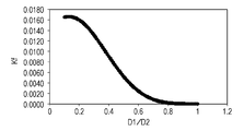
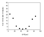
도 10을 참조하면, 제3 영역(7)의 개구(2C)의 지름이 증가함에 따라 비점 수차가 감소한다는 사실이 설명될 것이다. 도 10은 개구(2C)의 직경과 비점 수차의 변화 사이의 관계를 예시한다. 비점 수차는 개구(2C)의 개구 단명의 진원도가 10nm인 경우에 대응한다. 도 10은 개구들(2A 및 2B)이 이상적인 원형인 경우 개구(2C)로 인한 비점 수차의 값들을 예시한다. 도 10으로부터 알 수 있듯이, D2가 증가함에 따라 비점 수차가 감소한다. 그러므로, D1 < D2를 유지하는 동안 D2의 값을 증가시킴으로써, 개구(2C)의 진원도에 대한 비점 수차의 민감도가 감소될 수 있다. 이에 따라, 개구(2C)에서의 개구 단면의 진원도가 악화된 경우에도, 관계 D1 < D2를 유지하면서 D2를 설정함으로써, 수차가 작은 하전 입자 빔 렌즈가 제조될 수 있다.Referring to FIG. 10, it will be explained that the astigmatism decreases as the diameter of the
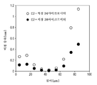
다음으로, 두께 방향으로의 제3 영역(7)의 진원도의 분포와 수차 기여율 사이의 관계가 설명될 것이다. 전술된 설계예에서 전극(2B)의 개구를 예시하는 도 15에 예시된 바와 같이, 제3 영역(7)은 각각이 두께 방향으로 10마이크로미터의 길이를 갖는 영역 S1 내지 영역 S9로 분할된다. 이들 영역이 상이한 진원도를 갖는 경우, 진원도에 대한 비점 수차의 민감도가 분석된다. 도 16에서, 수평축은 깊이 방향(각 영역의 중심에서의 깊이가 대표 위치로서 사용됨)의 영역 S1 내지 영역 S9의 위치를 나타내며, 수직축은 제3 영역(7) 전체의 수차에 대한 영역의 수차의 비율(기여율)을 나타낸다. 즉, 도 16은 이들 영역의 진원도가 동일한 경우 비점 수차에 대한 영역 S1 내지 영역 S9의 영향을 도시한다. 도 16으로부터 알 수 있는 바와 같이, 수차의 약 84%가 최외각 표면으로부터 20마이크로미터 내에 배치된 영역 S1, S2, S8, 및 S9에 의해 결정된다. 두께 방향으로 중간에 위치하는 영역들 S4, S5, 및 S6 각각의 기여율은 2% 이하인데 이것이 한계이다.Next, the relationship between the distribution of the roundness of the
다음으로, 진원도가 실제로 분포를 갖는 경우 수차의 크기 사이의 관계가 설명될 것이다. 도 17a는 영역 S1 내지 영역 S9의 진원도의 분포를 예시한다. 속이 빈 삼각형들은 영역 S1 내지 영역 S9가 동일한 진원도를 갖는 경우의 분포를 나타내고, 속이 빈 원들은 영역 S1 내지 영역 S9가 가장 작은 진원도를 갖고 진원도가 영역 S5를 향해 증가하는 경우의 분포를 나타내고, 속이 찬 원들은 진원도가 영역 S1으로부터 영역 S9으로 증가하는 경우의 분포를 나타낸다.Next, the relationship between the magnitudes of the aberrations will be described when the roundness is actually distributed. 17A illustrates the distribution of roundness in regions S1 to S9. The hollow triangles show the distribution when the regions S1 to S9 have the same roundness, and the hollow circles show the distribution when the regions S1 to S9 have the smallest roundness and the roundness increases toward the region S5. The circles represent the distribution when the roundness increases from the area S1 to the area S9.
실리콘이 도 9에 예시된 하나의 방향으로부터 딥 드라이 에칭된 경우에, 진원도는 속이 찬 원으로 표현된 분포를 가질 것이다. 실리콘이 전면 및 후면으로부터 딥 드라이 에칭되는 경우, 진원도는 속이 빈 원들로 표현된 분포를 가질 것이다. 이들 2개의 경우는 이들 분포가 실제 가공에 통상적으로 일어나기 때문에 중요하다. 도 17b는 비점 수차의 기여율을 예시한다. 도 17b의 지점들의 타입은 도 17a의 지점들의 타입에 대응한다. 속이 찬 원들의 경우, 최외각 표면 근처의 영역 S1 및 S2이 기여율은 낮고, 최외각 표면 반대편 근처의 영역 S8 및 S9의 기여율은 높다. 그 결과, 수차의 약 84%가 최외각 표면으로부터 20마이크로미터 내의 영역 S1, S2, S8, 및 S9에 의해 결정된다. 속이 빈 원들의 경우, 중간 영역 S4, S5, 및 S6의 기여율이 더 높다. 그러나, 이들 영역의 기여율이 여전히 낮기 때문에 총 수차에 대한 영향은 작다. 그 결과, 수차의 약 76%가 최외각 표면으로부터 20마이크로미터 내에 배치된 영역 S1, S2, S8, 및 S9에 의해 결정된다.In the case where silicon is deep dry etched from one direction illustrated in FIG. 9, the roundness will have a distribution expressed as a solid circle. If the silicon is deep dry etched from the front and back sides, the roundness will have a distribution expressed in hollow circles. These two cases are important because these distributions usually occur in actual processing. 17B illustrates the contribution of astigmatism. The type of points in FIG. 17B corresponds to the type of points in FIG. 17A. For solid circles, regions S1 and S2 near the outermost surface have a low contribution, and regions S8 and S9 near the outermost surface are high. As a result, about 84% of the aberrations are determined by regions S1, S2, S8, and S9 within 20 micrometers from the outermost surface. For the hollow circles, the contributions of the middle regions S4, S5, and S6 are higher. However, the contribution to the total aberration is small because the contribution rate of these areas is still low. As a result, about 76% of the aberration is determined by the regions S1, S2, S8, and S9 disposed within 20 micrometers from the outermost surface.
전술한 바와 같이, 진원도 분포의 경우 각각에서, 제3 영역(7)의 총 두께가 100마이크로미터라고 하더라도, 수차의 대부분이 최외각 표면으로부터 20마이크로미터 내의 영역들에 의해 결정된다. 특히, 최외각 표면들의 기여율이 높다. 진원도가 두께 내에서 몇 배씩 달라지는 도 17a의 속이 빈 원들의 경우에, 최외각 표면들의 영향이 가장 크다. 두께 방향의 영역의 개구의 프로파일에서 형상 또는 표면 조건의 변화가 과도하지 않으면, 전면 및 후면 최외각 표면에서의 진원도만이 측정될 수 있으며, 진원도의 평균값이 영역의 평균 진원도로서 사용될 수 있다. 이러한 측정에 기반하여 결정된 대표 진원도가 충분히 우수한 근사치로 수차를 검사하는데 사용될 수 있다. 그러므로, 두께 방향의 진원도의 분포를 측정하는 것이 어려운 경우, 측정 방법이 이러한 방식으로 간략화될 수 있으며, 이로써 본 발명에 따른 개구 단면의 형상이 검사될 수 있다.As mentioned above, in each case of the roundness distribution, even if the total thickness of the
도 18은 제3 영역(7)의 직경이 34마이크로미터 및 38마이크로미터인 경우에 대해 진원도 분포가 도 17a의 속이 찬 원으로 표현된다고 가정하고 획득된 실제 비점 수차의 값들을 도시한다. 전술한 바와 같이, 직경이 클수록, 수차는 작아진다. 특히, 최외각 표면으로부터 20마이크로미터 내의 영역의 비점 수차의 차이가 크다. 이로 인해, 직격 변화에 관해, 최외각 표면들의 영향이 가장 크다. 그러므로, 진원도와 마찬가지로, 두께 방향으로의 영역 내의 개구의 프로파일에서 형상 또는 표면 조건의 변화가 과도하지 않으면, 전면 및 후면 최외각 표면에서의 대표 직경들의 평균은 영역의 평균 대표 직경으로서 사용될 수 있다.FIG. 18 shows the values of the actual astigmatism obtained, assuming that the roundness distribution is represented by the solid circle of FIG. 17A for the case where the diameter of the
다음으로, 본 실시예를 제조하는 방법이 설명될 것이다. 제1 영역, 제2 영역, 및 제3 영역은 제1 계면(13) 및 제2 계면(14)을 통해 서로 접합된다. 각각이 제1 영역 및 제2 영역이 될 두께가 6마이크로미터인 디바이스 층, 임베디드 산화막 층, 및 핸들 층(handle layer)을 갖는 실리콘-온-인슐레이터(SOI) 기판들이 준비된다. 우선, 고정밀도 포토리소그래피 및 실리콘의 드라이 에칭을 수행함으로써 개구들(2A 및 2B)이 디바이스 층에 형성된다. 그 후, 기판 전체가 열적 산화된다. 포토리소그래피 및 실리콘의 딥 드라이 에칭을 수행함으로써, 제3 영역과 동일한 88마이크로미터의 두께를 갖는 실리콘 기판에 개구(2C)가 형성된다. 그 후, 개구(2A 및 2B)가 형성된 SOI 기판의 디바이스 층들은 열적 산화막을 통해 개구(2C)가 형성된 실리콘 기판의 전면 및 후면에 직접 접합된다. 그 후, 2장의 SOI 웨이퍼의 핸들 층 및 임베디드 산화막 층, 개구(2A 및 2B의 접합 계면 이외의 열적 산화막을 차례로 제거함으로써, 각각이 제1 영역, 제2 영역, 및 제3 영역을 갖는 전극들(3A, 3B, 및 3C)이 형성될 수 있다. 본 실시예는 계면(13 및 14)을 통해 접합되는 접합 구조뿐 아니라, 다른 위치에 계면을 갖거나 계면을 갖지 않는 구조에서도 동일한 효과를 갖는다. 그러나, 특히, 계면(13 및 14)을 통해 영역들이 접합된 경우에 형상의 정밀도가 요구되는 개구들(2A 및 2B)을 형성하는 단계 및 개구(2C)를 형성하는 단계가 별도로 수행될 수 있다. 그러므로, 에칭 조건들의 제어가 정밀하게 수행될 수 있고, 수율이 개선될 수 있다. 특히, 거의 완벽한 진원도가 요구되는 개구들(2A 및 2B)의 두께가 감소될 수 있으며, 이로써 그 개구들이 고정밀도로 형성될 수 있다. 더구나, 개구(2C)가 비교적 낮은 정밀도를 갖는 프로세스를 이용하여 형성될 수 있어서, 제조 비용 및 단계의 개수가 줄어들며 수율이 개선된다. 또한, 단결정 실리콘을 사용함으로써 포토리소그래피 또는 드라이 에칭과 같은 고정밀도 개구를 형성하는 프로세스 및 평탄도가 높은 표면을 통한 웨이퍼 접합에 의해 본 발명에 따른 전극이 높은 정밀도로 형성될 수 있다. 이에 따라, 이 설계예에서와 같이, 대략 수십 마이크로미터의 직경을 갖는 개구가 대략 수 나노미터의 진원도로 형성될 수 있다.Next, a method of manufacturing this embodiment will be described. The first region, the second region, and the third region are bonded to each other through the
접합이 수행되어 개구들(2A 및 2B) 및 개구(2C)가 계면(13 및 14)에서 서로 접촉하는 경우, D1 < D2를 충족시키는 직격이 서로 상이하기 때문에 개구들의 에지는 동일한 위치에 위치하지 않는다. 그러므로, 접합 전에 개구들(2A 및 2C)을 열적 산화하는 경우, 열적 산화막의 두께가 분포를 갖기 때문에 돌출부가 에지 부위에 형성됨에도 불구하고, 접합 프로세스는 이들 돌출부에 의해 방해받지 않는다.When the joining is performed such that the
제2 실시예Second Embodiment
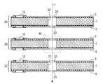
도 12를 참조하여, 본 발명의 제2 실시예가 설명될 것이다. 도 11은 하전 입자 빔 렌즈의 단면도이다. 제1 실시예서와 동일한 기능을 갖는 부위는 동일한 도면부호로 표시될 것이며, 제1 실시예와 동일한 효과의 설명은 생략될 것이다. 본 실시예 및 제1 실시예에서, 전극(3A, 3B, 및 3C) 각각은 복수의 개구(2A), 복수의 개구(2B), 복수의 개구(2C)를 갖는다. 본 실시예에서, 도 11에 예시된 바와 같이, 하전 입자 빔 렌즈는 5개의 개구가 전극 각각에 형성된 렌즈 어레이이다.Referring to Fig. 12, a second embodiment of the present invention will be described. 11 is a sectional view of a charged particle beam lens. The parts having the same functions as those in the first embodiment will be denoted by the same reference numerals, and the description of the same effects as in the first embodiment will be omitted. In this embodiment and the first embodiment, each of the
개구(2C)의 직경은 개구(2A)의 직경보다 더 크다. 개구(2C)의 직경이 인접 개구 사이의 피치(pitch)보다 작기 때문에, 인접 개구(2C)들은 제3 영역에서 서로 연결되지 않는다. 그러므로, 전극 전체의 강도를 감소시키지 않고 렌즈 어레이가 형성될 수 있다.The diameter of the opening 2C is larger than the diameter of the
더구나, 개구 단면이 고정밀도로 형성될 수 있기 때문에, 렌즈 어레이의 개별 렌즈들의 개구 단면의 진원도 변동이 줄어들 수 있다. 렌즈 어레이의 개별 렌즈의 진원도는 불규칙 오차를 갖기 때문에, 개별적으로 진원도를 보정하는 것은 매우 어렵다. 그러므로, 개구 단면의 진원도의 변동을 감소시킴으로써, 대형 렌즈 어레이가 형성될 수 있다.Moreover, since the opening cross section can be formed with high precision, the roundness variation of the opening cross section of the individual lenses of the lens array can be reduced. Since the roundness of the individual lenses of the lens array has an irregular error, it is very difficult to correct the roundness individually. Therefore, by reducing the variation in the roundness of the opening cross section, a large lens array can be formed.
특히, 전극이 제1 실시예와 동일한 방법으로 제조될 수 있는 접합 구조를 갖는 경우, 개구 단면들의 변동이 충분히 감소될 수 있다. 접합의 정렬 정밀도가 낮으면, 개구(2A 및 2B) 사이의 위치 변화가 일어난다. 그러나, 이러한 위치 변화는 렌즈 어레이 전체에서의 위치 변화가 균일하기 때문에 용이하게 보정될 수 있다. 그러므로, 이러한 구조는 대형 렌즈 어레이에 알맞다.In particular, when the electrode has a junction structure that can be manufactured in the same manner as in the first embodiment, the variation of the opening cross sections can be sufficiently reduced. If the alignment accuracy of the joint is low, a position change between the
제3 실시예Third Embodiment
도 19는 본 발명에 따른 하전 입자 빔 렌즈를 사용한 멀티 하전 입자 빔 노광 장치를 예시한다. 본 실시예는 개별적으로 투영계(projection system)를 갖는 소위 멀티-컬럼 타입이다.19 illustrates a multi charged particle beam exposure apparatus using a charged particle beam lens according to the present invention. This embodiment is a so-called multi-column type with a projection system individually.
전자원(108)으로부터 애노드 전극(110)을 통해 방출된 방사 전자빔이 크로스오버 조정 광학계(111)로 인해 조사 광학계 크로스오버(112)를 형성한다.The radiation electron beam emitted from the
전자원(108)으로서 LaB6 또는 BaO/W(디스펜서 캐소드) 등 이른바 열이온 전자원(thermionic electron source)이 사용된다.As the
크로스오버 조정 광학계(111)는 2단 정전 렌즈를 포함한다. 제1 단 및 제2 단의 정전 렌즈 각각은 음의 전압이 중간 전극에 인가되고 상위 전극 및 하위 전극은 접지되어 있는 3개의 전극을 포함하는 이른바 단독 정전 렌즈이다.The crossover adjustment
조사 광학계 크로스오버(112)로부터 광각으로 확산되는 전자 빔은 콜리메이터(collimator) 렌즈(115)에 의해 평행하게 되어, 애퍼처 어레이(117)에 평행해진 빔이 조사된다. 애퍼처 어레이(117)는 전자 빔을 멀티 전자 빔(118)으로 분할한다. 집속 렌즈 어레이(119)가 멀티 전자 빔(118)을 블랭커 어레이(blanker array)(122)로 개별적으로 집속한다.The electron beam diffused from the irradiation
집속 렌즈 어레이(119)는 음의 전압이 중간 전극에 인가되고 상위 전극 및 하위 전극은 접지되어 있는 다수의 개구를 갖는 3개의 전극을 포함하는 단독 정전 렌즈 어레이이다.The focusing
애퍼처 어레이(117)는 애퍼처 어레이(117)가 NA(집속의 반각(half-angle of focus))를 정의하는 역할을 하도록 집속 렌즈 어레이(119)의 동공면(pupil plane)의 위치(집속 렌즈 어레이(119)의 전방 포커스의 위치)에 배치된다.The
독립적인 편향 전극을 갖는 디바이스인 블랭커 어레이(122)는 리소그래픽 패턴 생성 회로(102), 비트맵 변환 회로(103), 및 귀선 소거(blanking) 지령 회로(106)에 의해 생성되는 귀선 소거 신호에 기반한 리소그래픽 패턴에 따라 개별적인 빔들의 온/오프 제어를 수행한다.The
빔-온 상태에서는 블랭커 어레이(122)의 편향 전극에 전압이 인가되지 않는다. 빔-오프 상태에서는 블랭커 어레이(122)의 편향 전극에 전압이 인가되어 멀티 전자 빔들이 편향된다. 블랭커 어레이(122)에 의해 편향된 멀티 전자 빔(125)이 블랭커 어레이(122) 뒤에 배치된 스톱 애퍼처 어레이(123)에 의해 차단되어 그 빔이 중단된다.In the beam-on state, no voltage is applied to the deflection electrode of the
본 실시예에서, 블랭커 어레이는 각각 블랭커 어레이(122) 및 스톱 애퍼처 어레이(123)과 동일한 구조를 갖는 제2 블랭커 어레이(127) 및 제2 스톱 애퍼처 어레이(128)가 제2 단에 배치되는 2단 구조를 갖는다.In the present embodiment, the blanker array includes a second
블랭커 어레이(122)를 통과한 멀티 전자 빔은 제2 집속 렌즈 어레이(126)에 의해 제2 블랭커 어레이(127)에 집속된다. 그 후, 멀티 전자 빔들은 제3 집속 렌즈 및 제4 집속 렌즈에 의해 웨이퍼(133)에 집속된다. 집속 렌즈 어레이(119)와 마찬가지로, 제2 집속 렌즈 어레이(126), 제3 집속 렌즈 어레이(130), 및 제4 집속 렌즈 어레이(132) 각각이 단독 정전 렌즈 어레이이다.The multi electron beam passing through the
특히, 제4 집속 렌즈 어레이(132)는 축소율이 100인 대물 렌즈이다. 이에 따라, (FWHM에서 스팟 직경이 2마이크로미터인) 블랭커 어레이(122)의 중간 촬상 면의 전자 빔(121)은 웨이퍼(133)의 표면에서 1/100로 축소되어 FWHM에서 약 20nm의 스팟 직경을 갖는 멀티 전자 빔의 영상을 형성한다. 제4 집속 렌즈 어레이(132)는 본 발명의 제2 실시예에 따른 하전 입자 빔 렌즈 어레이이다.In particular, the fourth focusing
웨이퍼에 대한 멀티 전자 빔의 스캔이 편향기(131)를 사용함으로써 수행될 수 있다. 편향기(131)는 4단 대향 전극을 포함하는데, 이로써 x 및 y 방향의 2-스테이지 편향이 수행될 수 있다(간단히, 2단 편향기들이 하나의 유닛으로 예시됨). 편향기(131)는 편향 신호 생성 회로(104)에 의해 생성된 신호에 따라 구동된다.Scanning of the multiple electron beams onto the wafer can be performed by using the
패턴이 형성되면서, 웨이퍼(133)는 스테이지(134)에 의해 X 방향으로 연속적으로 이동된다. 웨이퍼에 대한 전자 빔(135)이 레이저 길이 측정 기계에 의해 획득된 실시간 측정 결과에 기반하여 편향기(131)에 의해 Y 방향으로 편향된다. 리소그래픽 패턴에 따라 블랭커 어레이(122) 및 제2 블랭커 어레이(127)에 의해 빔의 온/오프 제어가 개별적으로 수행된다. 이로 인해, 원하는 패턴이 고속으로 웨이퍼(133)에 형성될 수 있다.As the pattern is formed, the
본 발명에 따른 하전 입자 빔 렌즈를 이용함으로써, 수차가 작은 집속이 실현된다. 그 때문에, 미세한 패턴을 형성할 수 있는 멀티 하전 입자 빔 노광 장치가 실현될 수 있다. 또한, 큰 면적에서 멀티 빔이 통과하는 개구가 형성되는 경우조차 전극은 큰 두께를 가질 수 있으며, 이로써 멀티 빔의 개수가 증가될 수 있다. 그래서, 고속으로 패턴을 형성하는 하전 입자 빔 노광 장치가 실현될 수 있다.By using the charged particle beam lens according to the present invention, focusing with small aberration is realized. Therefore, a multi-charged particle beam exposure apparatus capable of forming a fine pattern can be realized. In addition, even in the case where an opening through which the multi-beams pass in a large area is formed, the electrode may have a large thickness, thereby increasing the number of multi-beams. Thus, a charged particle beam exposure apparatus that forms a pattern at high speed can be realized.
본 발명에 따른 하전 입자 빔 렌즈 어레이는 집속 렌즈 어레이(119), 제2 집속 렌즈 어레이(126), 및 제3 집속 렌즈 어레이(130) 중 어느 하나로서 사용될 수 있다.The charged particle beam lens array according to the present invention may be used as any one of the focusing
본 발명에 따른 하전 입자 빔 렌즈는 도 19에 예시된 복수의 빔을 사용하는 것 대신에 단일 빔을 사용하는 하전 입자 빔 리소그래피 장치로서 사용될 수 있다. 이 경우에도, 작은 수차만 갖는 렌즈를 사용함으로써, 미세한 패턴을 형성하는 하전 입자 빔 노광 장치가 실현될 수 있다.The charged particle beam lens according to the present invention can be used as a charged particle beam lithography apparatus using a single beam instead of using the plurality of beams illustrated in FIG. 19. Even in this case, by using a lens having only a small aberration, a charged particle beam exposure apparatus for forming a fine pattern can be realized.
본 발명은 예시적인 실시예들을 참조하여 설명되었지만, 개시된 실시예들로 제한되지 않는다는 점이 이해되어야 한다. 다음의 청구항의 범위는 이러한 모든 변형예 및 균등 구조 및 기능을 포괄하도록 최광의로 해석되어야 한다.Although the present invention has been described with reference to exemplary embodiments, it should be understood that it is not limited to the disclosed embodiments. The scope of the following claims is to be accorded the broadest interpretation so as to encompass all such modifications and equivalent structures and functions.
본 출원은 2011년 3월 15일에 출원된 일본 특허출원 제2011-056813호에 대한 우선권을 주장하며, 그 내용은 전체적으로 참조로서 원용된다.This application claims the priority of Japanese Patent Application No. 2011-056813 for which it applied on March 15, 2011, The content is taken in into consideration as a whole.
Claims (10)
광축 방향으로 연장되는 법선을 갖는 제1 표면 및 상기 제1 표면의 반대 측의 제2 표면을 갖는 평판을 포함하는 전극 - 상기 전극은 상기 제1 표면으로부터 상기 제2 표면으로 연장되는 관통-홀을 가짐 - 을 포함하며,
상기 법선에 수직인 평면을 따라 절취된 상기 관통-홀의 단면으로서 개구 단면이 정의되고, 상기 개구 단면의 회귀 분석을 수행함으로써 획득되는 원의 직경으로서 대표 직경이 정의되는 경우, 상기 제1 표면 측에 있는 제1 영역의 개구 단면의 대표 직경과 상기 제2 표면 측에 있는 제2 영역의 개구 단면의 대표 직경은 각각 상기 제1 표면과 상기 제2 표면 사이에 배치된 전극의 영역인 제3 영역의 개구 단면의 대표 직경보다 작은 정전 하전 입자 빔 렌즈.Electrostatic charged particle beam lens,
An electrode comprising a flat surface having a first surface having a normal extending in the optical axis direction and a second surface opposite the first surface, the electrode having a through-hole extending from the first surface to the second surface; Contains-,
If an opening cross section is defined as a cross section of the through-hole cut along a plane perpendicular to the normal, and a representative diameter is defined as a diameter of a circle obtained by performing a regression analysis of the opening cross section, The representative diameter of the opening cross section of the first region in which the first region is located and the representative diameter of the opening cross section of the second region on the side of the second surface are respectively the regions of the electrode disposed between the first surface and the second surface. Electrostatic charged particle beam lens smaller than the representative diameter of the opening cross section.
Applications Claiming Priority (3)
| Application Number | Priority Date | Filing Date | Title |
|---|---|---|---|
| JPJP-P-2011-056813 | 2011-03-15 | ||
| JP2011056813A JP2012195096A (en) | 2011-03-15 | 2011-03-15 | Charged particle beam lens and exposure apparatus using the same |
| PCT/JP2012/001773 WO2012124319A1 (en) | 2011-03-15 | 2012-03-14 | Charged particle beam lens and exposure apparatus using the same |
Publications (1)
| Publication Number | Publication Date |
|---|---|
| KR20130135335A true KR20130135335A (en) | 2013-12-10 |
Family
ID=45932473
Family Applications (1)
| Application Number | Title | Priority Date | Filing Date |
|---|---|---|---|
| KR1020137026268A KR20130135335A (en) | 2011-03-15 | 2012-03-14 | Charged particle beam lens and exposure apparatus using the same |
Country Status (4)
| Country | Link |
|---|---|
| US (1) | US20140151570A1 (en) |
| JP (1) | JP2012195096A (en) |
| KR (1) | KR20130135335A (en) |
| WO (1) | WO2012124319A1 (en) |
Families Citing this family (1)
| Publication number | Priority date | Publication date | Assignee | Title |
|---|---|---|---|---|
| JP6720861B2 (en) * | 2016-12-28 | 2020-07-08 | 株式会社ニューフレアテクノロジー | Multi-beam aperture set and multi-charged particle beam drawing device |
Family Cites Families (28)
| Publication number | Priority date | Publication date | Assignee | Title |
|---|---|---|---|---|
| US3899711A (en) * | 1973-05-09 | 1975-08-12 | Gen Electric | Laminated multi-apertured electrode |
| US4200794A (en) * | 1978-11-08 | 1980-04-29 | Control Data Corporation | Micro lens array and micro deflector assembly for fly's eye electron beam tubes using silicon components and techniques of fabrication and assembly |
| JPS58500306A (en) * | 1981-02-27 | 1983-02-24 | ベ−コ インスツルメンツ インコ−ポレイテツド | Method for manufacturing screen lens array plate |
| US4533794A (en) * | 1983-05-23 | 1985-08-06 | Beveridge Harold N | Electrode for electrostatic transducer |
| US4902898A (en) * | 1988-04-26 | 1990-02-20 | Microelectronics Center Of North Carolina | Wand optics column and associated array wand and charged particle source |
| US5155412A (en) * | 1991-05-28 | 1992-10-13 | International Business Machines Corporation | Method for selectively scaling a field emission electron gun and device formed thereby |
| JPH0562611A (en) * | 1991-09-05 | 1993-03-12 | Hitachi Ltd | Cathode-ray tube provided with plate electrode for electron gun |
| DE69204629T2 (en) * | 1991-11-29 | 1996-04-18 | Motorola Inc | Manufacturing method of a field emission device with integral electrostatic lens arrangement. |
| JPH0814881A (en) * | 1994-06-28 | 1996-01-19 | Nippon Steel Corp | Method of calculating diameter value by use of three-dimensionally measuring unit |
| JPH08241688A (en) * | 1995-03-03 | 1996-09-17 | Hitachi Ltd | Pattern ion beam projecting device |
| JP2000188068A (en) * | 1998-12-22 | 2000-07-04 | Hitachi Ltd | Color cathode ray tube |
| JP2001283756A (en) * | 2000-03-31 | 2001-10-12 | Canon Inc | Electron optical system array, charged particle beam exposure device using it and device manufacturing method |
| US6741016B2 (en) * | 2001-06-14 | 2004-05-25 | Hewlett-Packard Development Company, L.P. | Focusing lens for electron emitter with shield layer |
| KR100496643B1 (en) * | 2003-10-25 | 2005-06-20 | 한국전자통신연구원 | Self-aligned multi-layer metal film electro-lens of a micro-column electron beam apparatus and method for fabricating same |
| US7045794B1 (en) * | 2004-06-18 | 2006-05-16 | Novelx, Inc. | Stacked lens structure and method of use thereof for preventing electrical breakdown |
| JP4625317B2 (en) * | 2004-12-03 | 2011-02-02 | ナガヤマ アイピー ホールディングス リミテッド ライアビリティ カンパニー | Phase plate for phase contrast electron microscope, method for producing the same, and phase contrast electron microscope |
| US7515253B2 (en) * | 2005-01-12 | 2009-04-07 | Kla-Tencor Technologies Corporation | System for measuring a sample with a layer containing a periodic diffracting structure |
| EP1941528B9 (en) * | 2005-09-06 | 2011-09-28 | Carl Zeiss SMT GmbH | Particle-optical arrangement with particle-optical component |
| JP5159035B2 (en) | 2005-10-28 | 2013-03-06 | キヤノン株式会社 | Lens array and charged particle beam exposure apparatus including the lens array |
| WO2008090380A1 (en) * | 2007-01-25 | 2008-07-31 | Nfab Limited | Improved particle beam generator |
| WO2010037832A2 (en) * | 2008-10-01 | 2010-04-08 | Mapper Lithography Ip B.V. | Electrostatic lens structure |
| JP5428682B2 (en) | 2009-09-10 | 2014-02-26 | 株式会社リコー | Image forming apparatus and image forming system |
| KR101041369B1 (en) * | 2009-11-19 | 2011-06-15 | 한국기초과학지원연구원 | High throughput apparatus and method for multiple sample analysis |
| JP2012195097A (en) * | 2011-03-15 | 2012-10-11 | Canon Inc | Charged particle beam lens and exposure apparatus using the same |
| JP5669636B2 (en) * | 2011-03-15 | 2015-02-12 | キヤノン株式会社 | Charged particle beam lens and exposure apparatus using the same |
| JP5744579B2 (en) * | 2011-03-15 | 2015-07-08 | キヤノン株式会社 | Charged particle beam lens and exposure apparatus using the same |
| JP5886663B2 (en) * | 2012-03-21 | 2016-03-16 | 株式会社日立ハイテクノロジーズ | Electron beam application device and lens array |
| JP2013239667A (en) * | 2012-05-17 | 2013-11-28 | Canon Inc | Electrode of charged particle beam electrostatic lens and manufacturing method of the same, charged particle beam electrostatic lens, and charged particle beam exposure device |
-
2011
- 2011-03-15 JP JP2011056813A patent/JP2012195096A/en not_active Abandoned
-
2012
- 2012-03-14 WO PCT/JP2012/001773 patent/WO2012124319A1/en active Application Filing
- 2012-03-14 US US14/004,845 patent/US20140151570A1/en active Granted
- 2012-03-14 KR KR1020137026268A patent/KR20130135335A/en not_active Application Discontinuation
Also Published As
| Publication number | Publication date |
|---|---|
| WO2012124319A1 (en) | 2012-09-20 |
| US20140151570A1 (en) | 2014-06-05 |
| JP2012195096A (en) | 2012-10-11 |
Similar Documents
| Publication | Publication Date | Title |
|---|---|---|
| WO2012124324A1 (en) | Charged particle beam lens and exposure apparatus using the same | |
| JP3763446B2 (en) | Electrostatic lens, electron beam drawing apparatus, charged beam application apparatus, and device manufacturing method | |
| US20220392734A1 (en) | Certain improvements of multi-beam generating and multi-beam deflecting units | |
| JP5439375B2 (en) | Standard member for calibration, scanning electron microscope using the same, and calibration method for scanning electron microscope | |
| US8963099B2 (en) | Electrode of electrostatic lens and method of manufacturing the same | |
| JP2013004216A (en) | Electric charge particle beam lens | |
| TW200952022A (en) | Projection lens arrangement | |
| TW201248674A (en) | Drawing apparatus and method of manufacturing article | |
| JP2009505384A (en) | Particle optics | |
| JP2013004680A (en) | Charged particle beam lens | |
| WO2012124322A1 (en) | Charged particle beam lens and exposure apparatus using the same | |
| US6768118B2 (en) | Electron beam monitoring sensor and electron beam monitoring method | |
| US20140091229A1 (en) | Electrode for a charged particle beam lens | |
| JP4615816B2 (en) | Electron lens, charged particle beam exposure apparatus using the electron lens, and device manufacturing method | |
| KR20130135335A (en) | Charged particle beam lens and exposure apparatus using the same | |
| JP2007123599A (en) | Charged particle beam lens array and charged particle beam exposure device using the same | |
| JP5669636B2 (en) | Charged particle beam lens and exposure apparatus using the same | |
| US20140349235A1 (en) | Drawing apparatus, and method of manufacturing article | |
| JP2006049703A (en) | Electrically charged particle beam lens array and electrically charged particle beam exposure device using the same | |
| JP4627454B2 (en) | Deflector and multi-charged particle beam writing apparatus using the same | |
| JP2005116719A (en) | Device for multielectron beam drawing apparatus and its manufacturing method | |
| JP2013030567A (en) | Charged particle beam lens array | |
| JP2013165234A (en) | Charged particle optical system, charged particle beam device, and method of manufacturing article | |
| JP2012204624A (en) | Lithography apparatus and method of manufacturing article |
Legal Events
| Date | Code | Title | Description |
|---|---|---|---|
| A201 | Request for examination | ||
| E902 | Notification of reason for refusal | ||
| E902 | Notification of reason for refusal | ||
| E601 | Decision to refuse application |