KR20130111280A - Optoelectric hybrid substrate - Google Patents
Optoelectric hybrid substrate Download PDFInfo
- Publication number
- KR20130111280A KR20130111280A KR1020130022798A KR20130022798A KR20130111280A KR 20130111280 A KR20130111280 A KR 20130111280A KR 1020130022798 A KR1020130022798 A KR 1020130022798A KR 20130022798 A KR20130022798 A KR 20130022798A KR 20130111280 A KR20130111280 A KR 20130111280A
- Authority
- KR
- South Korea
- Prior art keywords
- light
- insulating layer
- opto
- core
- layer
- Prior art date
Links
Images


Classifications
-
- G—PHYSICS
- G02—OPTICS
- G02B—OPTICAL ELEMENTS, SYSTEMS OR APPARATUS
- G02B6/00—Light guides; Structural details of arrangements comprising light guides and other optical elements, e.g. couplings
- G02B6/10—Light guides; Structural details of arrangements comprising light guides and other optical elements, e.g. couplings of the optical waveguide type
-
- G—PHYSICS
- G02—OPTICS
- G02B—OPTICAL ELEMENTS, SYSTEMS OR APPARATUS
- G02B6/00—Light guides; Structural details of arrangements comprising light guides and other optical elements, e.g. couplings
- G02B6/24—Coupling light guides
- G02B6/42—Coupling light guides with opto-electronic elements
- G02B6/4201—Packages, e.g. shape, construction, internal or external details
- G02B6/4204—Packages, e.g. shape, construction, internal or external details the coupling comprising intermediate optical elements, e.g. lenses, holograms
- G02B6/4214—Packages, e.g. shape, construction, internal or external details the coupling comprising intermediate optical elements, e.g. lenses, holograms the intermediate optical element having redirecting reflective means, e.g. mirrors, prisms for deflecting the radiation from horizontal to down- or upward direction toward a device
-
- G—PHYSICS
- G02—OPTICS
- G02B—OPTICAL ELEMENTS, SYSTEMS OR APPARATUS
- G02B6/00—Light guides; Structural details of arrangements comprising light guides and other optical elements, e.g. couplings
- G02B6/24—Coupling light guides
- G02B6/42—Coupling light guides with opto-electronic elements
- G02B6/4201—Packages, e.g. shape, construction, internal or external details
- G02B6/4204—Packages, e.g. shape, construction, internal or external details the coupling comprising intermediate optical elements, e.g. lenses, holograms
- G02B6/4206—Optical features
-
- H—ELECTRICITY
- H05—ELECTRIC TECHNIQUES NOT OTHERWISE PROVIDED FOR
- H05K—PRINTED CIRCUITS; CASINGS OR CONSTRUCTIONAL DETAILS OF ELECTRIC APPARATUS; MANUFACTURE OF ASSEMBLAGES OF ELECTRICAL COMPONENTS
- H05K1/00—Printed circuits
- H05K1/02—Details
-
- H—ELECTRICITY
- H05—ELECTRIC TECHNIQUES NOT OTHERWISE PROVIDED FOR
- H05K—PRINTED CIRCUITS; CASINGS OR CONSTRUCTIONAL DETAILS OF ELECTRIC APPARATUS; MANUFACTURE OF ASSEMBLAGES OF ELECTRICAL COMPONENTS
- H05K1/00—Printed circuits
- H05K1/02—Details
- H05K1/0274—Optical details, e.g. printed circuits comprising integral optical means
-
- G—PHYSICS
- G02—OPTICS
- G02B—OPTICAL ELEMENTS, SYSTEMS OR APPARATUS
- G02B6/00—Light guides; Structural details of arrangements comprising light guides and other optical elements, e.g. couplings
- G02B6/24—Coupling light guides
- G02B6/42—Coupling light guides with opto-electronic elements
- G02B6/4201—Packages, e.g. shape, construction, internal or external details
- G02B6/4274—Electrical aspects
- G02B6/4283—Electrical aspects with electrical insulation means
-
- G—PHYSICS
- G02—OPTICS
- G02B—OPTICAL ELEMENTS, SYSTEMS OR APPARATUS
- G02B6/00—Light guides; Structural details of arrangements comprising light guides and other optical elements, e.g. couplings
- G02B6/24—Coupling light guides
- G02B6/42—Coupling light guides with opto-electronic elements
- G02B6/43—Arrangements comprising a plurality of opto-electronic elements and associated optical interconnections
-
- H—ELECTRICITY
- H05—ELECTRIC TECHNIQUES NOT OTHERWISE PROVIDED FOR
- H05K—PRINTED CIRCUITS; CASINGS OR CONSTRUCTIONAL DETAILS OF ELECTRIC APPARATUS; MANUFACTURE OF ASSEMBLAGES OF ELECTRICAL COMPONENTS
- H05K2201/00—Indexing scheme relating to printed circuits covered by H05K1/00
- H05K2201/10—Details of components or other objects attached to or integrated in a printed circuit board
- H05K2201/10007—Types of components
- H05K2201/10121—Optical component, e.g. opto-electronic component
Landscapes
- Physics & Mathematics (AREA)
- General Physics & Mathematics (AREA)
- Optics & Photonics (AREA)
- Engineering & Computer Science (AREA)
- Microelectronics & Electronic Packaging (AREA)
- Optical Integrated Circuits (AREA)
- Optical Couplings Of Light Guides (AREA)
Abstract
Description
본 발명은 광학 소자가 실장된 전기 회로 기판과 광도파로가 적층된 광전기 혼재 기판에 관한 것이다. The present invention relates to an electric circuit board on which an optical element is mounted and an opto-electric hybrid board on which an optical waveguide is laminated.
최근의 전자 기기 등에서는, 전송 정보량의 증가에 수반하여, 전기 배선에 더하여, 광 배선이 채용되고 있다. 그러한 것으로서, 예컨대 도 7에 도시하는 바와 같이, 절연층(51)의 표면에 전기 배선(52)이 형성되어 이루어지는 전기 회로 기판(Eo)과, 이 전기 회로 기판(Eo)의 상기 절연층(51)의 이면[전기 배선(52)의 형성면과 반대측의 면]에 적층된 광도파로(광 배선)(Wo)[언더클래드층(56), 코어(57), 오버클래드층(58)]와, 상기 전기 배선(52)의 형성면 중, 상기 광도파로(Wo)의 양단부에 대응하는 부분에 실장된 발광 소자(11) 및 수광 소자(12)를 포함하는 광전기 혼재 기판이 제안되어 있다(예컨대, 특허문헌 1 참조). 그리고, 상기 광도파로(Wo)의 양단부는, 상기 전기 회로 기판(Eo)에 대하여 45˚ 경사진 경사면으로 형성되고, 그 경사면에 위치하는 코어(57) 부분이 광 반사면(57a)으로 되어 있다. 또한, 상기 발광 소자(11) 및 수광 소자(12)에 대응하는 상기 절연층(51)의 부분에, 광로용의 관통 구멍(55)이 형성되고, 상기 발광 소자(11)와 일단부의 광 반사면(57a) 사이 및 상기 수광 소자(12)와 타단부의 광 반사면(57a) 사이에서, 상기 관통 구멍(55)을 통해 광(L)이 전파 가능하게 되어 있다.Background Art In recent years, optical wirings have been adopted in addition to electrical wirings in connection with an increase in the amount of transmission information. As such, for example, as shown in FIG. 7, the electric circuit board E o , in which the
상기 광전기 혼재 기판에서의 광(L)은 다음과 같이 전파된다. 우선, 발광 소자(11)로부터 광(L)이 일단부의 광 반사면(57a)을 향해 발광한다. 그 광(L)은 상기 절연층(51)에 형성된 광로용의 관통 구멍(55)을 통과한 후, 광도파로(Wo)의 일단부(도 7에서는 좌단부)의 언더클래드층(56)을 빠져 나가, 코어(57) 일단부의 광 반사면(57a)에서 반사되어(광로가 90˚ 변환하여), 코어(57) 내에서, 축방향으로 진행한다. 그리고, 그 광(L)은 코어(57)의 타단부(도 7에서는 우단부)의 광 반사면(57a)에서 반사되어(광로가 90˚ 변환하여), 수광 소자(12)를 향해 진행한다. 계속해서, 그 광(L)은 타단부의 언더클래드층(56)을 빠져 나가 출사되고, 광로용의 관통 구멍(55)을 통과한 후, 수광 소자(12)에서 수광된다. Light L in the opto-electric hybrid substrate is propagated as follows. First, the light L is emitted from the
그러나, 상기 발광 소자(11)로부터 발광된 광(L), 및 타단부의 광 반사면(57a)에서 반사된 광(L)은 도 7에 도시하는 바와 같이 확산한다. 이 때문에 광(L)의 전파 효율이 낮다. 그래서, 도 8에 도시하는 바와 같이, 상기 광로용의 관통 구멍(55)의 개구면에 렌즈(60)를 부착하여, 그 관통 구멍(55)을 통과하는 광(L)을, 상기 렌즈(60)의 작용에 의해, 평행광 내지 집속광으로 하는 것이 제안되어 있다(예컨대, 특허문헌 2 참조). 이것의 경우, 상기한 바와 같이 광(L)을 평행광 내지 집속광으로 함으로써, 광(L)의 전파가 효율적이게 된다.However, the light L emitted from the
그러나, 상기 렌즈(60)는 부착되는 것이기 때문에, 렌즈(60)의 부착 공정이 필요하게 되어, 생산성이 저하된다고 하는 문제가 있다. 또한, 그 부착 때문에, 부착 위치의 정밀도에 변동이 생긴다고 하는 문제도 있다. However, since the
본 발명은 이러한 사정을 감안하여 이루어진 것으로, 생산성을 저하시키지 않고, 또한 안정된 위치 정밀도로, 광학 소자와 코어 사이의 광로에서의 렌즈를 형성할 수 있는 광전기 혼재 기판의 제공을 그 목적으로 한다. This invention is made | formed in view of such a situation, Comprising: It aims at providing the opto-electric hybrid board which can form the lens in the optical path between an optical element and a core with a stable positional precision, without reducing productivity.
상기한 목적을 달성하기 위해, 본 발명의 광전기 혼재 기판은, 절연층 표면에 전기 배선이 형성되어 이루어지는 전기 회로 기판과, 이 전기 회로 기판의 전기 배선 형성면에 실장된 광학 소자와, 상기 전기 회로 기판의 상기 절연층의 이면측에 형성된 광도파로를 구비하고, 그 광도파로의 코어의 단부에, 광을 반사하여 상기 코어와 상기 광학 소자 사이의 광 전파를 가능하게 하는 반사부가 형성된 광전기 혼재 기판으로서, 상기 절연층은 투광성 재료로 이루어지고, 상기 코어에 형성된 상기 반사부와 상기 광학 소자 사이의 광로에 대응하는 상기 절연층의 부분은 렌즈부로 형성되는 구성을 취한다. In order to achieve the above object, the opto-electric hybrid board of the present invention includes an electric circuit board on which an electric wiring is formed on an insulating layer surface, an optical element mounted on an electric wiring forming surface of the electric circuit board, and the electric circuit. An opto-electric hybrid substrate having an optical waveguide formed on the back side of the insulating layer of a substrate, and having a reflecting portion at the end of the core of the optical waveguide for reflecting light to enable light propagation between the core and the optical element. The insulating layer is made of a light-transmissive material, and the portion of the insulating layer corresponding to the optical path between the reflecting portion and the optical element formed in the core is formed of a lens portion.
본 발명의 광전기 혼재 기판은, 절연층이 투광성 재료로 이루어지기 때문에, 코어에 형성된 반사부와 광학 소자 사이의 광로에 대응하는 상기 절연층의 부분에, 광로용의 관통 구멍을 형성할 필요가 없다. 또한, 상기 광로가 되는 절연층의 부분이 렌즈부로 형성되기 때문에, 그 렌즈부는, 절연층의 일부이며, 별개 부재의 렌즈를 부착할 필요가 없다. 이와 같이, 본 발명의 광전기 혼재 기판은, 절연층에 광로용의 관통 구멍을 형성하는 공정 및 광로 부분에 렌즈를 부착하는 공정을 필요로 하지 않는 것이기 때문에, 생산성을 향상시킬 수 있다. 또한, 상기한 바와 같이, 절연층에 별개 부재의 렌즈를 부착할 필요가 없기 때문에, 부착 위치의 변동이 생기지 않아, 상기 렌즈부를 안정된 위치 정밀도로 형성할 수 있다. In the opto-electric hybrid board of the present invention, since the insulating layer is made of a light-transmissive material, it is not necessary to form through-holes for the optical path in the portion of the insulating layer corresponding to the optical path between the reflecting portion formed in the core and the optical element. . Moreover, since the part of the insulating layer which becomes the said optical path is formed by the lens part, the lens part is a part of an insulating layer, and it is not necessary to attach the lens of a separate member. As described above, the opto-electric hybrid substrate of the present invention does not require a step of forming a through hole for an optical path in the insulating layer and a step of attaching a lens to the optical path portion, thereby improving productivity. In addition, as described above, since it is not necessary to attach the lens of the separate member to the insulating layer, the variation of the attachment position does not occur, and the lens portion can be formed with stable position accuracy.
특히, 상기 절연층의 투광성 재료가 감광성 수지이며, 상기 렌즈부가 포토리소그래피법일 때의 계조 노광에 의해 형성된 것인 경우에는, 한번의 포토리소그래피법에 의해, 렌즈부를 갖는 절연층이 형성될 수 있기 때문에, 생산성 및 렌즈부의 위치 정밀도가 우수하게 된다.In particular, when the light-transmissive material of the insulating layer is a photosensitive resin and the lens portion is formed by gradation exposure when the photolithography method is used, the insulating layer having the lens portion can be formed by one photolithography method. The productivity and the positional accuracy of the lens section are excellent.
또한, 상기 절연층에, 상기 전기 배선의 위치 결정용 얼라인먼트 마크가 형성되고, 상기 전기 배선이 상기 얼라인먼트 마크를 안표로 하여 형성되어 있는 경우에는, 상기 전기 배선의 위치 정밀도도 우수하게 된다.Moreover, when the alignment mark for positioning of the said electrical wiring is formed in the said insulating layer, and the said electrical wiring is formed with the alignment mark as the eye mark, the positional accuracy of the said electrical wiring becomes also excellent.
또한, 상기 절연층에, 상기 광학 소자의 위치 결정용 얼라인먼트 마크가 형성되고, 상기 광학 소자가 상기 얼라인먼트 마크를 안표로 하여 실장되어 있는 경우에는, 상기 광학 소자의 위치 정밀도도 우수하게 된다.Moreover, when the alignment mark for positioning of the optical element is formed in the insulating layer, and the optical element is mounted with the alignment mark as the eye mark, the positional accuracy of the optical element is also excellent.
그리고, 상기 절연층이 파장 600 ㎚ 이상의 광의 투과율이 70% 이상인 경우에는, 상기 절연층을 투과하는 광이 많아지기 때문에, 광의 결합 손실이 적어지게 된다.In the case where the insulating layer has a transmittance of 70% or more of light having a wavelength of 600 nm or more, the light passing through the insulating layer increases, so that the coupling loss of the light decreases.
또한, 상기 절연층이 150℃ 이상의 내열성을 갖는 내열층인 경우에는, 상기 광학 소자를 실장할 때의 열로 상기 렌즈부의 변형이 발생하지 않기 때문에, 적정한 렌즈의 집광 효과를 발휘하게 된다.Moreover, when the said insulating layer is a heat resistant layer which has heat resistance of 150 degreeC or more, since the deformation | transformation of the said lens part does not generate | occur | produce by the heat at the time of mounting the said optical element, the condensing effect of a suitable lens is exhibited.
도 1은 본 발명의 광전기 혼재 기판의 제1 실시형태를 모식적으로 도시하는 종단면도이다.
도 2의 (a)∼(d)는 상기 광전기 혼재 기판의 전기 회로 기판의 제작 공정을 모식적으로 도시하는 설명도이며, (e)는 상기 광전기 혼재 기판의 금속층의 에칭 공정을 모식적으로 도시하는 설명도이다.
도 3의 (a)∼(d)는 상기 광전기 혼재 기판의 광도파로의 제작 공정을 모식적으로 도시하는 설명도이다.
도 4는 본 발명의 광전기 혼재 기판의 제2 실시형태를 모식적으로 도시하는 종단면도이다.
도 5는 본 발명의 광전기 혼재 기판의 제3 실시형태를 모식적으로 도시하는 종단면도이다.
도 6은 본 발명의 광전기 혼재 기판의 제4 실시형태를 모식적으로 도시하는 종단면도이다.
도 7은 종래의 광전기 혼재 기판을 모식적으로 도시하는 종단면도이다.
도 8은 종래의 광 배선 기판을 모식적으로 도시하는 종단면도이다. 1 is a longitudinal cross-sectional view schematically showing a first embodiment of the opto-electric hybrid board of the present invention.
(A)-(d) is explanatory drawing which shows typically the manufacturing process of the electric circuit board of the said opto-electric hybrid board | substrate, (e) shows the etching process of the metal layer of the said opto-electric hybrid board | substrate typically. It is explanatory drawing to say.
FIG.3 (a)-(d) are explanatory drawing which shows typically the manufacturing process of the optical waveguide of the said optoelectronic mixed substrate.
4 is a longitudinal sectional view schematically showing a second embodiment of the opto-electric hybrid board of the present invention.
5 is a longitudinal cross-sectional view schematically showing a third embodiment of the opto-electric hybrid board of the present invention.
6 is a longitudinal cross-sectional view schematically showing a fourth embodiment of the opto-electric hybrid board of the present invention.
7 is a longitudinal sectional view schematically showing a conventional opto-electric hybrid board.
8 is a longitudinal sectional view schematically showing a conventional optical wiring board.
이어서, 본 발명의 실시형태를 도면에 기초하여 자세히 설명한다. Next, embodiment of this invention is described in detail based on drawing.
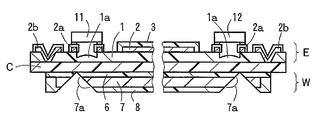
도 1은 본 발명의 광전기 혼재 기판의 제1 실시형태를 모식적으로 도시하는 종단면도이다. 이 실시형태의 광전기 혼재 기판은 절연층(1)의 표면에 전기 배선(2)이 형성되어 이루어지는 전기 회로 기판(E)과, 이 전기 회로 기판(E)의 전기 배선(2)의 형성면에 실장된 발광 소자(11) 및 수광 소자(12)와, 이 전기 회로 기판(E)의 절연층(1)의 이면에 형성된 광도파로(W)와, 이 광도파로(W)와 상기 전기 회로 기판(E)의 절연층(1)의 이면 사이에 형성된 금속층(M)을 구비한, 좌우 방향으로 연장되는 밴드형의 것으로 되어 있다. 또한, 상기 발광 소자(11) 및 수광 소자(12)에 대응하는 금속층(M)의 부분에, 광로용의 관통 구멍(5)이 형성되어 있다. 또한, 상기 발광 소자(11) 및 수광 소자(12)에 대응하는 광도파로(W)의 양단부에는, 역V자형의 절결부가 형성되고, 이 역V자의 경사면은 광도파로(W)의 코어(7)의 길이 방향에 대하여 45˚ 경사진 면으로 형성되어 있다. 이 경사면은, 광을 반사하여, 발광 소자(11)와 코어(7) 사이의 광 전파 및 수광 소자(12)와 코어(7) 사이의 광 전파를 가능하게 하는 반사면(7a)으로 되어 있다. 1 is a longitudinal cross-sectional view schematically showing a first embodiment of the opto-electric hybrid board of the present invention. The opto-electric hybrid board of this embodiment has an electrical circuit board (E) in which electrical wirings (2) are formed on the surface of the insulating layer (1), and the formation surface of the electrical wiring (2) of the electrical circuit boards (E). The mounted
그리고, 상기 절연층(1)은 투명한 합성 수지 등의 투광성 재료로 이루어지고, 상기 코어(7)의 일단부의 반사면(7a)과 상기 발광 소자(11) 사이의 광로에 대응하는 상기 절연층(1)의 부분이, 상기 발광 소자(11)측으로 팽창된 볼록형의 곡면을 갖는 렌즈부(1a)로 형성되어 있다. 상기 코어(7)의 타단부의 반사면(7a)과 상기 수광 소자(12) 사이의 광로에 대응하는 상기 절연층(1) 부분도, 마찬가지로 렌즈부(1a)로 형성되어 있다. 본 발명은 이와 같이 상기 절연층(1) 자체를 투광성 재료로 구성하고, 광로에 대응하는 상기 절연층(1)의 부분을 렌즈부(1a)로 형성한 것이 큰 특징이다. The
상기 광전기 혼재 기판에서의 광 전파는, 다음와 같이 하여 행해진다. 즉, 상기 발광 소자(11)로부터, 코어(7)의 일단부(도 1에서는 좌단부)의 반사면(7a)에 대하여, 확산형으로 광(L)이 발광한다. 그 광(L)은 우선, 상기 절연층(1)의 렌즈부(1a)를 통과한다. 이 통과시, 상기 렌즈부(1a)의 작용에 의해, 상기 확산된 광(L)을 평행광 내지 집속광으로 한다(도면에서는 평행광). 이어서, 그 광(L)은 금속층(M)에 형성된 광로용의 관통 구멍(5)을 통과한 후, 코어(7) 일단부의 반사면(7a)에서 반사되고, 코어(7) 내에서 축방향으로 진행한다. 그리고, 그 광(L)은 코어(7)의 타단부(도 1에서는 우단부)의 반사면(7a)에서 반사되고, 금속층(M)에 형성된 광로용의 관통 구멍(5)을 통과한 후, 상기 절연층(1)의 렌즈부(1a)를 통과한다. 이 통과시, 상기 렌즈부(1a)의 작용에 의해, 상기 광(L)을 집속광으로 한다. 그리고, 그 광은 수광 소자(12)에서 수광된다. 이와 같이, 발광 소자(11)로부터 출사되어 코어(7)의 일단부에 입사하는 광(L), 및 코어(7) 타단부의 반사면(7a)에서 반사되어 수광 소자(12)에 의해 수광되는 광(L)이 상기 절연층(1)의 렌즈부(1a)의 작용에 의해, 평행광 내지 집속광이 되기 때문에, 광(L)의 전파가 효율적이게 된다.Light propagation in the opto-electric hybrid board is performed as follows. That is, the light L emits light from the
또한, 상기 절연층(1)의 렌즈부(1a)는 절연층의 일부이기 때문에, 별개 부재의 렌즈를 부착할 필요가 없다. 이 때문에, 렌즈를 부착하는 공정이 불필요할 수 있고, 그 부착에 수반하는 부착 위치의 변동도 생기지 않는다. 즉, 상기 광전기 혼재 기판은 생산성이 우수하고, 렌즈부(1a)의 위치 정밀도도 우수하다. In addition, since the
또한, 이 실시형태에서는, 상기 전기 회로 기판(E)은 그 길이 방향의 양단부에서, 상기 절연층(1) 표면에, 광학 소자 실장용 패드(2a)가 노출된 상태로 형성되어 있고, 상기 절연층(1)을 관통하여 이면의 금속층(M)에 접촉하는 어스용 전극(2b)이 노출된 상태로 형성되어 있다. 이들 광학 소자 실장용 패드(2a) 및 어스용 전극(2b)은 상기 전기 배선(2)의 일부이며, 이들 이외의 전기 배선(2)의 부분은 커버레이(3)에 의해 피복되어 절연 보호되어 있다. Moreover, in this embodiment, the said electric circuit board E is formed in the state in which the optical
또한, 상기 광도파로(W)는, 언더클래드층(6)과, 이 언더클래드층(6)의 표면(도 1에서는 하면)에 정해진 패턴 형성된 코어(7)와, 이 코어(7)를 피복한 상태로 상기 언더클래드층(6) 표면에 형성된 오버클래드층(8)을 구비한다. 그리고, 상기 언더클래드층(6)은 그 이면[코어(7)의 형성면과 반대측의 면]에서 상기 금속층(M)에 접하고, 상기 금속층(M)에 형성된 광로용의 관통 구멍(5)에 들어가 매립되어 있다.The optical waveguide W covers the under
다음에, 상기 광전기 혼재 기판의 제조 방법에 대해서 설명한다[도 2의 (a)∼(e), 도 3의 (a)∼(d) 참조]. Next, the manufacturing method of the said opto-electric hybrid board | substrate is demonstrated (refer FIG.2 (a)-(e), FIG.3 (a)-(d)).
우선, 평탄형의 상기 금속층(M)[도 2의 (a) 참조]을 준비한다. 이 금속층(M)의 형성 재료로서는, 스테인리스, 42 알로이 등을 들 수 있고, 그 중에서도, 치수 정밀도 등의 관점에서, 스테인리스가 바람직하다. 또한, 상기 금속층(M)의 두께는 예컨대 10 ㎛∼100 ㎛의 범위 내로 설정된다. First, the flat metal layer M (see FIG. 2A) is prepared. Examples of the material for forming the metal layer M include stainless steel and 42 alloys. Among them, stainless steel is preferred from the viewpoint of dimensional accuracy and the like. In addition, the thickness of the said metal layer M is set in the range of 10 micrometers-100 micrometers, for example.
이어서, 도 2의 (a)에 도시하는 바와 같이, 상기 금속층(M) 표면에, 감광성 절연 수지를 도포하고, 포토리소그래피법으로 정해진 패턴의 절연층(1)을 형성한다. 이 실시형태에서는, 절연층(1)의 정해진 부분을 계조 노광에 의해 상기 렌즈부(1a)로 형성한다. 이와 동시에, 길이 방향의 양단부에, 금속층(M)에 접촉하는 어스용 전극(2b)을 형성하기 위해, 상기 금속층(M)의 표면을 노출시키는 구멍부(1b)를 형성한다. 이와 같이, 이 광전기 혼재 기판의 제조 방법에서는, 절연층(1)의 형성과 동시에, 그 절연층(1)의 정해진 부분을 렌즈부(1a)로 형성하기 때문에, 별개 부재의 렌즈를 부착하는 공정이 불필요하고, 생산성이 우수하며, 렌즈부(1a)를 형성하는 위치 정밀도도 우수하다. Next, as shown to Fig.2 (a), the photosensitive insulating resin is apply | coated to the said metal layer M surface, and the insulating
상기 절연층(1)의 형성 재료로서는, 예컨대 폴리이미드, 폴리에테르니트릴, 폴리에테르술폰, 폴리에틸렌테레프탈레이트, 폴리에틸렌나프탈레이트, 폴리염화비닐 등의 합성 수지, 실리콘계 졸겔 재료 등을 들 수 있다. 그 중에서도, 내열성 및 절연성이 우수하고, 파장 600 ㎚ 이상에서 전(全)광선 투과율 70% 이상을 갖는 감광성 폴리이미드가 바람직하다. 또한, 상기 발광 소자(11) 및 수광 소자(12)를 실장할 때의 열로 상기 렌즈부(1a)에 변형이 발생하지 않도록 하는 관점에서, 상기 절연층에 있어서, 150℃ 이상의 내열성을 갖는 형성 재료를 이용하는 것이 바람직하다. 상기 절연층(1)의 두께는, 예컨대 3 ㎛∼100 ㎛의 범위 내로 설정된다. 또한, 상기 전광선 투과율은 JIS K7105 「플라스틱의 광학적 특성 시험 방법」 5.5 「광선 투과율 및 전광선 반사율」에서 규정하는 적분식 광선 투과율 측정 장치 및 측정법에 따른 값이다. Examples of the material for forming the insulating
다음에, 도 2의 (b)에 도시하는 바와 같이, 상기 전기 배선[광학 소자 실장용 패드(2a) 및 어스용 전극(2b)을 포함함](2)을, 예컨대 세미애디티브법(semi-additive)으로 형성한다. 이 방법은 우선, 상기 절연층(1) 표면에, 스퍼터링 또는 무전해 도금 등에 의해, 구리나 크롬 등으로 이루어지는 금속막(도시 생략)을 형성한다. 이 금속막은 나중에 전해 도금을 행할 때의 시드층(전해 도금층 형성의 바탕이 되는 층)이 된다. 이어서, 상기 금속층(M), 절연층(1) 및 시드층을 포함하는 적층체의 양면에, 감광성 레지스트(도시 생략)를 라미네이트한 후, 상기 시드층이 형성되어 있는 측의 감광성 레지스트에, 포토리소그래피법으로, 상기 전기 배선[광학 소자 실장용 패드(2a) 및 어스용 전극(2b)을 포함함](2)의 패턴의 구멍부를 형성하고, 그 구멍부의 바닥에 상기 시드층의 표면 부분을 노출시킨다. 이어서, 전해 도금에 의해, 상기 구멍부의 바닥에 노출된 상기 시드층의 표면 부분에, 구리 등으로 이루어지는 전해 도금층을 적층 형성한다. 그리고, 상기 감광성 레지스트를 수산화나트륨 수용액 등에 의해 박리한다. 그 후, 상기 전해 도금층이 형성되어 있지 않은 시드층의 부분을 소프트 에칭에 의해 제거한다. 잔존한 시드층과 전해 도금층을 포함하는 적층 부분이 상기 전기 배선[광학 소자 실장용 패드(2a) 및 어스용 전극(2b)을 포함함](2)이다. 여기서는, 상기 세미애디티브법을 설명했지만, 서브트랙티브법이어도 좋다. Next, as shown in Fig. 2B, the electric wiring (including the optical
그리고, 도 2의 (c)에 도시하는 바와 같이, 상기 전기 배선[광학 소자 실장용 패드(2a) 및 어스용 전극(2b)을 포함함](2)의 표면에, 니켈 등으로 이루어지는 무전해 도금층(도시 생략)을 형성한 후, 상기 광학 소자 실장용 패드(2a) 및 어스용 전극(2b)을 제외한 전기 배선(2)의 부분에, 폴리이미드 수지 등으로 이루어지는 감광성 절연 수지를 도포하고, 포토리소그래피법에 의해, 커버레이(3)를 형성한다. As shown in Fig. 2C, an electroless made of nickel or the like is formed on the surface of the electrical wiring (including the optical
이어서, 도 2의 (d)에 도시하는 바와 같이, 상기 광학 소자 실장용 패드(2a) 및 어스용 전극(2b)에 형성된 상기 무전해 도금층(도시 생략)을 에칭에 의해 제거한 후, 그 제거 흔적에, 금이나 니켈 등으로 이루어지는 전해 도금층(4)을 형성한다. 이와 같이 하여, 상기 금속층(M)의 표면에, 전기 회로 기판(E)이 형성된다. Subsequently, as shown in Fig. 2 (d), after removing the electroless plating layer (not shown) formed on the optical
다음에, 상기 금속층(M)과 전기 회로 기판(E)을 포함하는 적층체의 양면에, 감광성 레지스트(도시 생략)를 라미네이트한다. 그 후, 상기 금속층(M)의 이면측[전기 회로 기판(E)과 반대측의 면측]의 감광성 레지스트 중, 광로용의 관통 구멍 형성 예정부에 대응하는 부분에, 포토리소그래피법에 의해, 구멍부를 형성하고, 그 구멍부의 바닥(도면에서는 상면)에 상기 금속층(M)의 이면 부분을 노출시킨다. Next, photosensitive resist (not shown) is laminated on both surfaces of the laminate including the metal layer M and the electric circuit board E. FIG. Subsequently, in the photosensitive resist on the back surface side (surface side opposite to the electric circuit board E) of the metal layer M, the portion corresponding to the through hole formation scheduled portion for the optical path is formed by the photolithography method. It forms and exposes the back surface part of the said metal layer M in the bottom (upper surface in drawing) of the said hole part.
그리고, 도 2의 (e)에 도시하는 바와 같이, 상기 구멍부의 바닥에 노출된 상기 금속층(M) 부분을, 그 금속층(M)의 금속 재료에 따른 에칭용 수용액(예컨대, 스테인리스층의 경우는, 염화 제2철 수용액)을 이용하여 에칭함으로써 제거하고, 그 제거 흔적(R)의 바닥(도면에서는 상면)에 상기 절연층(1)을 노출시킨다. 그 후, 상기 감광성 레지스트를 수산화나트륨 수용액 등에 의해 박리한다. 상기 제거 흔적(R)은 광로용의 관통 구멍(5)이다. As shown in FIG. 2E, the metal layer M portion exposed to the bottom of the hole portion is etched in an aqueous solution for etching according to the metal material of the metal layer M (eg, in the case of a stainless steel layer). It removes by etching using a ferric chloride aqueous solution, and exposes the said insulating
그리고, 상기 금속층(M)의 이면에 광도파로(W)[도 3의 (d) 참조]를 형성하기 위해, 우선, 도 3의 (a)에 도시하는 바와 같이, 상기 금속층(M)의 이면(도면에서는 하면)에, 언더클래드층(6)의 형성 재료인 감광성 수지를 도포한 후, 그 도포층을 조사선에 의해 노광하고 경화시켜, 언더클래드층(6)을 형성한다. 이 언더클래드층(6)은 상기 금속층(M) 중, 에칭 제거된 광로용의 관통 구멍(5)[제거 흔적(R)]에 들어가 매립된 상태로 형성된다. 상기 언더클래드층(6)의 두께[절연층(1)의 이면으로부터의 두께]는, 예컨대 5 ㎛∼200 ㎛의 범위 내로 설정된다. 또한, 광도파로(W)의 형성시[상기 언더클래드층(6), 하기 코어(7), 하기 오버클래드층(8)의 형성시]에는, 상기 금속층(M)의 이면은 위로 향해진다.Then, in order to form the optical waveguide W (see FIG. 3 (d)) on the back surface of the metal layer M, first, as shown in FIG. 3A, the back surface of the metal layer M is shown. After applying the photosensitive resin which is a forming material of the
이어서, 도 3의 (b)에 도시하는 바와 같이, 상기 언더클래드층(6)의 표면(도면에서는 하면)에, 포토리소그래피법으로, 정해진 패턴의 코어(7)를 형성한다. 또한, 상기 코어(7)의 두께는 5 ㎛∼200 ㎛의 범위 내로 설정되고, 폭은 5 ㎛∼200 ㎛의 범위 내로 설정된다. 상기 코어(7)의 형성 재료로서는, 예컨대 상기 언더클래드층(6)과 같은 감광성 수지를 들 수 있고, 상기 언더클래드층(6) 및 하기 오버클래드층(8)[도 3의 (c) 참조]의 형성 재료보다 굴절율이 큰 재료가 이용된다. 이 굴절율의 조정은, 예컨대 상기 언더클래드층(6), 코어(7), 오버클래드층(8)의 각 형성 재료의 종류의 선택이나 조성 비율을 조정하여 이루어질 수 있다. Subsequently, as shown in FIG. 3B, the
다음에, 도 3의 (c)에 도시하는 바와 같이, 상기 코어(7)를 피복하도록, 상기 언더클래드층(6) 표면(도면에서는 하면)에, 포토리소그래피법으로, 오버클래드층(8)을 형성한다. 이 오버클래드층(8)의 두께[언더클래드층(6)의 표면으로부터의 두께]는 상기 코어(7)의 두께 이상이고, 200 ㎛ 이하로 설정된다. 상기 오버클래드층(8)의 형성 재료로서는, 예컨대 상기 언더클래드층(6)과 같은 감광성 수지를 들 수 있다. Next, as shown in FIG. 3C, the
그리고, 도 3의 (d)에 도시하는 바와 같이, 상기 전기 회로 기판(E)의 광학 소자 실장용 패드(2a)에 대응하는 (도면에서는 아래쪽에 위치하는)광도파로(W) 부분(양단부)을, 레이저 가공 또는 끼인각 90˚의 회전날 등을 이용한 절삭 가공 등에 의해, 코어(7)의 길이 방향에 대하여 45˚ 경사진 경사면으로 형성한다. 이 경사면의 코어(7)의 부분이 광 반사면(7a)으로서 작용한다. 이와 같이 하여, 상기 금속층(M)의 이면에, 광도파로(W)가 형성된다. As shown in Fig. 3D, the optical waveguide W portion (both ends) (corresponding to the bottom in the drawing) corresponding to the
그 후, 상기 광학 소자 실장용 패드(2a)에, 발광 소자(11) 및 수광 소자(12)(도 1 참조)를 실장하고, 도 1에 도시하는 광전기 혼재 기판을 얻는다. Thereafter, the
도 4는 본 발명의 광전기 혼재 기판의 제2 실시형태를 모식적으로 도시하는 종단면도이다. 이 실시형태의 광전기 혼재 기판은 상기 제1 실시형태의 광전기 혼재 기판(도 1 참조)에 있어서, 금속층(M)이 설치되지 않은 것이다. 그 이외의 부분은 상기 제1 실시형태와 마찬가지이며, 같은 부분에는, 동일한 부호를 붙이고 있다. 4 is a longitudinal sectional view schematically showing a second embodiment of the opto-electric hybrid board of the present invention. In the opto-electric hybrid substrate of this embodiment, the metal layer M is not provided in the opto-electric hybrid substrate (see FIG. 1) of the first embodiment. The other part is the same as that of the said 1st Embodiment, and the same code | symbol is attached | subjected to the same part.
이 실시형태의 광전기 혼재 기판은, 예컨대 박리성 기대(基臺) 위에, 상기 제1 실시형태와 마찬가지로 하여, 전기 회로 기판(E)을 형성한 후, 그 박리성 기대를 박리하고, 상기 전기 회로 기판(E)의 절연층(1)의 이면[전기 배선(2)의 형성면과 반대측의 면]에, 상기 제1 실시형태와 마찬가지로 하여, 광도파로(W)를 형성함으로써 제작된다.In the photovoltaic mixed substrate of this embodiment, for example, on the peelable base, the electrical circuit board E is formed in the same manner as in the first embodiment, and then the peelable base is peeled off, and the electrical circuit It is produced by forming the optical waveguide W on the back surface (surface opposite to the formation surface of the electrical wiring 2) of the insulating
도 5는 본 발명의 광전기 혼재 기판의 제3 실시형태를 모식적으로 도시하는 종단면도이다. 이 실시형태의 광전기 혼재 기판은 상기 제1 실시형태의 광전기 혼재 기판(도 1 참조)에 있어서, 금속층(M)과 광도파로(W)가 투광성을 갖는 접착 시트(C)에 의해 접착되어 있는 것이며, 금속층(M)에 형성된 광로용의 관통 구멍(5)에 언더클래드층(6)은 들어가 매립되지 않는다. 그 이외의 부분은 상기 제1 실시형태와 마찬가지이며, 같은 부분에는, 동일한 부호를 붙이고 있다. 5 is a longitudinal cross-sectional view schematically showing a third embodiment of the opto-electric hybrid board of the present invention. In the opto-electric hybrid substrate of this embodiment, the metal layer M and the optical waveguide W are adhered to each other by the adhesive sheet C having light transparency in the opto-electric hybrid substrate (see FIG. 1) of the first embodiment. The under
이 실시형태의 광전기 혼재 기판은, 상기 제1 실시형태와 마찬가지로 하여, 금속층(M) 표면에, 전기 회로 기판(E)을 형성한 후, 그 금속층(M) 이면에, 다른 공정에서 제작된 광도파로(W)를, 상기 투광성을 갖는 접착 시트(C)에 의해 접착함으로써 제작된다. 또한, 이 투광성을 갖는 접착 시트(C)의 형성 재료로서는, 예컨대 에폭시 수지, 아크릴 수지, 페놀 수지 등을 들 수 있다. 또한 그 접착 시트(C)의 두께는, 예컨대 1 ㎛∼200 ㎛의 범위 내로 설정된다. The photovoltaic mixed substrate of this embodiment is similar to the first embodiment, and after the electric circuit board E is formed on the surface of the metal layer M, the light produced in another process on the back surface of the metal layer M is formed. It is produced by adhering the waveguide W to the light-transmitting adhesive sheet C. Moreover, an epoxy resin, an acrylic resin, a phenol resin etc. are mentioned as a formation material of the adhesive sheet (C) which has this light transmittance, for example. In addition, the thickness of the adhesive sheet C is set in the range of 1 micrometer-200 micrometers, for example.
도 6은 본 발명의 광전기 혼재 기판의 제4 실시형태를 모식적으로 도시하는 종단면도이다. 이 실시형태의 광전기 혼재 기판은 상기 제2 실시형태의 광전기 혼재 기판(도 4 참조)에 있어서, 전기 회로 기판(E)과 광도파로(W)가 상기 제3 실시형태와 같은 투광성을 갖는 접착 시트(C)에 의해 접착되어 있는 것이다. 그 이외의 부분은 상기 제2 실시형태와 마찬가지이며, 같은 부분에는, 동일한 부호를 붙이고 있다. 6 is a longitudinal cross-sectional view schematically showing a fourth embodiment of the opto-electric hybrid board of the present invention. In the opto-electric hybrid board of this embodiment, in the opto-electric hybrid board (see FIG. 4) of the second embodiment, the electric circuit board E and the optical waveguide W have the same transparency as in the third embodiment. It is bonded by (C). The other part is the same as that of the said 2nd Embodiment, and the same code | symbol is attached | subjected to the same part.
이 실시형태의 광전기 혼재 기판은, 각각 다른 공정에서 제작된 전기 회로 기판(E)과 광도파로(W)를, 상기 투광성을 갖는 접착 시트(C)에 의해 접착함으로써 제작된다. The opto-electric hybrid board of this embodiment is produced by adhering the electric circuit board E and the optical waveguide W produced at different processes with the adhesive sheet C having the light-transmitting property.
또한, 상기 각 실시형태에서는, 렌즈부(1a)를 갖는 절연층(1)을 포토리소그래피법에 의해 형성했지만, 레이저 에칭 또는 금형 성형에 의해 형성하여도 좋다. In addition, in each said embodiment, although the insulating
또한, 상기 각 실시형태에서는, 절연층(1) 중, 발광 소자(11)에 대응하는 부분과 수광 소자(12)에 대응하는 부분 양부분에, 렌즈부(1a)를 형성했지만, 광(L)의 전파 효율이 충분한 경우 등에서는, 경우에 따라, 어느 한쪽에만 렌즈부(1a)를 형성하여도 좋다. Moreover, in each said embodiment, although the
또한, 상기 각 실시형태에서는, 절연층(1)에 형성하는 렌즈부(1a)를 볼록 렌즈로 했지만, 확산하는 광을 억제 내지 집속할 수 있으면, 오목 렌즈 등, 다른 렌즈여도 좋다. In addition, in each said embodiment, although the
또한, 상기 각 실시형태에서, 절연층(1)을 형성할 때에, 그 절연층(1) 표면에, 상기 포토리소그래피법, 레이저 에칭, 또는 금형 성형에 의해, 전기 배선(2)의 위치 결정용 얼라인먼트 마크를 형성하여도 좋다. 이와 같이 하면, 절연층(1)에서의 전기 배선(2)의 형성 위치 정밀도가 향상된다. 또한, 상기 얼라인먼트 마크의 위치는, 예컨대 절연층(1)의 상하, 좌우, 네 코너 등에 설정된다. In each of the above embodiments, when the insulating
그리고, 상기 각 실시형태에서, 절연층(1)을 형성할 때에, 그 절연층(1) 표면에, 상기 포토리소그패리법, 레이저 에칭, 또는 금형 성형에 의해, 발광 소자(11) 및 수광 소자(12)의 위치 결정용 얼라인먼트 마크를 형성하여도 좋다. 이와 같이 하면, 절연층(1)에서의 발광 소자(11) 및 수광 소자(12)의 실장 위치 정밀도가 향상된다. 또한, 상기 얼라인먼트 마크의 위치는, 예컨대 광학 소자 실장용 패드(2a) 근방에 설정된다.In each of the above embodiments, when the insulating
또한, 상기 각 실시형태에서, 절연층(1)을 형성할 때에, 그 절연층(1)에, 상기 포토리소그래피법, 레이저 에칭, 또는 금형 성형에 의해, 비아(비아홀)를 형성하여도 좋다. In each of the above embodiments, when the insulating
다음에, 실시예에 대해서 비교예와 함께 설명한다. 단, 본 발명은 실시예에 한정되는 것은 아니다. Next, examples will be described together with comparative examples. However, the present invention is not limited to the embodiments.
[실시예][Example]
[실시예 1∼4][Examples 1 to 4]
상기 제1 실시형태를 실시예 1로 하고, 상기 제2 실시형태를 실시예 2로 하며, 상기 제3 실시형태를 실시예 3으로 하고, 상기 제4 실시형태를 실시예 4로 하였다. 모두, 두께 20 ㎛의 스테인리스박(SUS304H-TA: 금속층)의 표면에, 포토리소그래피법으로, 렌즈부를 갖는 폴리이미드 수지제의 절연층을 형성하였다. 그 포토리소그래피법에 이용한 포토마스크는 렌즈부에 대응하는 부분의 평균 투과율이 다른 부분의 80%이고, 단계적으로 내린 것으로 하였다. 상기 절연층은 파장 600 ㎚에서 전광선 투과율이 70%였다. The said 1st Embodiment was made into Example 1, the said 2nd Embodiment was made into Example 2, the said 3rd Embodiment was made into Example 3, and the said 4th Embodiment was made into Example 4. In each case, the insulating layer made of polyimide resin which has a lens part was formed in the surface of the stainless steel foil (SUS304H-TA: metal layer) of thickness 20micrometer by the photolithographic method. The photomask used in the photolithography method is assumed to have a stage in which the average transmittance of the portion corresponding to the lens portion is 80% of the other portion. The insulating layer had a total light transmittance of 70% at a wavelength of 600 nm.
[비교예][Comparative Example]
상기 실시예 1에서, 절연층에 렌즈부를 형성하지 않는 것을 비교예로 하였다. 그 이외의 부분은 상기 실시예 1과 마찬가지로 하였다. In Example 1, the lens was not formed in the insulating layer as a comparative example. The other part was the same as that of the said Example 1.
[광의 결합 손실][Coupling loss of light]
발광 소자로서, VCSEL(Ulm Photonics사 제조, 850-05-1×1)을 준비하고, 수광 소자로서, PD(Roithner laser Technik사 제조, TPD-8D12-014)를 준비하였다. 그리고, 상기 VCSEL로부터 발광된 광을 직접, 상기 PD로 수광했을 때의 광량(Io)을 측정하였다. 이어서, 상기 VCSEL 및 PD를 실장한 후, 상기 VCSEL로부터 발광된 광을, 상기 광전기 혼재 기판의 광도파로의 코어에 통과시켜 상기 PD로 수광했을 때의 광량(I)을 측정하였다. 그리고, 그 비(Io/I)를 산출하고, 그 값을 상기 광전기 혼재 기판에서의 광의 전파 손실로 하였다. 한편, 컷 백(cut back)법으로 구한, 상기 광도파로의 중간부에서의 광의 전파 손실은 0.1 dB/㎝였다. 이 값과 상기 광전기 혼재 기판에서의 광의 전파 손실로부터 상기 광전기 혼재 기판에서의 결합 손실을 산출하였다. 그리고, 그 결과를 하기의 표 1에 함께 표기하였다.As a light emitting element, VCSEL (made by Ulm Photonics, 850-05-1x1) was prepared, and PD (Roithner laser Technik make, TPD-8D12-014) was prepared as a light receiving element. The light amount I o when the light emitted from the VCSEL was directly received by the PD was measured. Subsequently, after mounting the VCSEL and the PD, the light amount I when the light emitted from the VCSEL was passed through the core of the optical waveguide of the opto-electric hybrid substrate and received by the PD was measured. And the ratio (I o / I) was calculated and the value was made into the propagation loss of the light in the said optoelectronic hybrid substrate. On the other hand, the propagation loss of light in the middle of the optical waveguide, which was obtained by the cut back method, was 0.1 dB / cm. The coupling loss in the opto-electric hybrid substrate was calculated from this value and the propagation loss of light in the opto-electric hybrid substrate. And, the results are shown together in Table 1 below.

상기 표 1의 결과로부터, 절연층에 렌즈부가 형성된 실시예 1∼4는 결합 손실이 작고, 절연층에 렌즈부가 형성되어 있지 않은 비교예는 결합 손실이 큰 것을 알 수 있다. From the results in Table 1, it can be seen that Examples 1 to 4 in which the lens portion was formed in the insulating layer had a small coupling loss, and that in Comparative Examples in which the lens portion was not formed in the insulating layer had a large coupling loss.
본 발명의 광전기 혼재 기판은 광학 소자와 코어 사이의 결합 손실을 작게 할 경우에 이용 가능하다. The opto-electric hybrid board of the present invention can be used when the coupling loss between the optical element and the core is reduced.
E: 전기 회로 기판 W: 광도파로
L: 광 1: 절연층
1a: 렌즈부 2: 전기 배선
7: 코어 7a: 반사면
11: 발광 소자 12: 수광 소자E: electric circuit board W: optical waveguide
L: light 1: insulation layer
1a: lens unit 2: electrical wiring
7:
11: light emitting element 12: light receiving element
Claims (6)
상기 절연층은 투광성 재료로 이루어지고, 상기 코어에 형성된 상기 반사부와 상기 광학 소자 사이의 광로에 대응하는 상기 절연층의 부분은 렌즈부로 형성되어 있는 것을 특징으로 하는 광전기 혼재 기판. An electrical circuit board having electrical wiring formed on the surface of the insulating layer, an optical element mounted on the electrical wiring forming surface of the electrical circuit board, and an optical waveguide formed on the rear surface side of the insulating layer of the electrical circuit board; A photovoltaic hybrid substrate having a reflector formed at an end of a core of the optical waveguide to reflect light to enable light propagation between the core and the optical element.
And the insulating layer is made of a light-transmissive material, and a portion of the insulating layer corresponding to the optical path between the reflecting portion and the optical element formed in the core is formed of a lens portion.
Applications Claiming Priority (2)
| Application Number | Priority Date | Filing Date | Title |
|---|---|---|---|
| JPJP-P-2012-077272 | 2012-03-29 | ||
| JP2012077272A JP5877749B2 (en) | 2012-03-29 | 2012-03-29 | Manufacturing method of opto-electric hybrid board |
Publications (2)
| Publication Number | Publication Date |
|---|---|
| KR20130111280A true KR20130111280A (en) | 2013-10-10 |
| KR102094552B1 KR102094552B1 (en) | 2020-03-27 |
Family
ID=47884156
Family Applications (1)
| Application Number | Title | Priority Date | Filing Date |
|---|---|---|---|
| KR1020130022798A KR102094552B1 (en) | 2012-03-29 | 2013-03-04 | Optoelectric hybrid substrate |
Country Status (6)
| Country | Link |
|---|---|
| US (1) | US9335497B2 (en) |
| EP (1) | EP2645142A1 (en) |
| JP (1) | JP5877749B2 (en) |
| KR (1) | KR102094552B1 (en) |
| CN (1) | CN103364893A (en) |
| TW (1) | TWI578040B (en) |
Cited By (3)
| Publication number | Priority date | Publication date | Assignee | Title |
|---|---|---|---|---|
| KR20170076655A (en) * | 2014-10-24 | 2017-07-04 | 닛토덴코 가부시키가이샤 | Optical/electric hybrid substrate, and production method therefor |
| KR20170076685A (en) * | 2014-10-28 | 2017-07-04 | 닛토덴코 가부시키가이샤 | Optical-electric hybrid circuit board |
| WO2024058376A1 (en) * | 2022-09-16 | 2024-03-21 | 주식회사 엘지에너지솔루션 | Optical communication device using conformal coating layer as optical waveguide |
Families Citing this family (16)
| Publication number | Priority date | Publication date | Assignee | Title |
|---|---|---|---|---|
| EP2809358B1 (en) | 2012-01-31 | 2022-07-13 | Surfacide, LLC | Hard surface disinfection system and method |
| JP2014041181A (en) * | 2012-08-21 | 2014-03-06 | Hitachi Chemical Co Ltd | Substrate with lens and production method therefor, and optical waveguide with lens |
| JP2014238491A (en) * | 2013-06-07 | 2014-12-18 | 日東電工株式会社 | Opto-electric hybrid module |
| TW201506481A (en) | 2013-07-02 | 2015-02-16 | Sumitomo Bakelite Co | Optical module member, optical module, and electronic equipment |
| JP6319762B2 (en) * | 2013-10-31 | 2018-05-09 | 日東電工株式会社 | Opto-electric hybrid board and manufacturing method thereof |
| CN103763855B (en) * | 2014-01-28 | 2016-08-24 | 华进半导体封装先导技术研发中心有限公司 | Photoelectricity printed board and preparation method thereof |
| US9829663B2 (en) * | 2014-02-25 | 2017-11-28 | Empire Technology Development Llc | Silicon chip with refractive index gradient for optical communication |
| JP6525240B2 (en) * | 2014-10-24 | 2019-06-05 | 日東電工株式会社 | Opto-electric hybrid board and its manufacturing method |
| CN105629401A (en) * | 2014-10-28 | 2016-06-01 | 富士康(昆山)电脑接插件有限公司 | Photoelectric conversion device |
| JP6674691B2 (en) * | 2014-12-10 | 2020-04-01 | 日東電工株式会社 | Opto-electric hybrid board |
| CN104777564B (en) * | 2015-04-24 | 2017-08-11 | 华进半导体封装先导技术研发中心有限公司 | A kind of chip support plate and preparation method thereof |
| CN104793288A (en) * | 2015-04-30 | 2015-07-22 | 上海美维科技有限公司 | Manufacturing method of printed circuit boards with optical waveguide couplers |
| JP6623344B2 (en) | 2016-03-22 | 2019-12-25 | 日東電工株式会社 | Optical waveguide laminate and manufacturing method thereof |
| JP6713922B2 (en) * | 2016-12-21 | 2020-06-24 | 日本特殊陶業株式会社 | Wiring board for optical element mounting |
| US10025044B1 (en) * | 2017-01-17 | 2018-07-17 | International Business Machines Corporation | Optical structure |
| US11768338B2 (en) * | 2021-05-27 | 2023-09-26 | Taiwan Semiconductor Manufacturing Company, Ltd. | Optical interconnect structure, package structure and fabricating method thereof |
Citations (5)
| Publication number | Priority date | Publication date | Assignee | Title |
|---|---|---|---|---|
| JP2002258081A (en) | 2001-02-28 | 2002-09-11 | Fujitsu Ltd | Optical wiring board, manufacturing method of the same, and multi-layer optical wiring |
| JP2003255166A (en) * | 2002-02-28 | 2003-09-10 | Matsushita Electric Ind Co Ltd | Solid optical waveguide and its manufacturing method, optical module, and optical transmission system |
| JP2004361858A (en) * | 2003-06-06 | 2004-12-24 | Sharp Corp | Optical waveguide with micro lens and its manufacturing method |
| KR20090112585A (en) * | 2008-04-24 | 2009-10-28 | 닛토덴코 가부시키가이샤 | Optical/electrical hybrid substrate producing method |
| JP2009288341A (en) | 2008-05-27 | 2009-12-10 | Nitto Denko Corp | Opto-electric hybrid module and manufacturing method thereof |
Family Cites Families (15)
| Publication number | Priority date | Publication date | Assignee | Title |
|---|---|---|---|---|
| US5101454A (en) * | 1991-02-20 | 1992-03-31 | At&T Bell Laboratories | Light emitting diode with multifaceted reflector to increase coupling efficiency and alignment tolerance |
| JP2002189137A (en) * | 2000-12-20 | 2002-07-05 | Nippon Telegr & Teleph Corp <Ntt> | Optical wiring board |
| JP2004302188A (en) * | 2003-03-31 | 2004-10-28 | Hitachi Cable Ltd | Electric wiring substrate with optical waveguide |
| KR100558438B1 (en) * | 2003-06-25 | 2006-03-10 | 삼성전기주식회사 | Optical Switch manufacturing method |
| JP2005017678A (en) * | 2003-06-26 | 2005-01-20 | Ricoh Co Ltd | Optical semiconductor device and, method for manufacturing optical semiconductor device, optical semiconductor system and method for manufacturing optical semiconductor system, and optical interconnection module |
| JP2005181645A (en) * | 2003-12-19 | 2005-07-07 | Sony Corp | Optical waveguide, manufacturing method therefor, and optical information processor |
| JP2006038958A (en) * | 2004-07-22 | 2006-02-09 | Sharp Corp | Condensing element and its manufacturing method, and photoelectric wiring board and its manufacturing method |
| JP2006052992A (en) * | 2004-08-10 | 2006-02-23 | Fuji Xerox Co Ltd | Inspection method of optical waveguide wiring board or photoelectric mixed mounting circuit board |
| JP2006208527A (en) * | 2005-01-26 | 2006-08-10 | Fuji Xerox Co Ltd | Circuit module with optical waveguide and method of manufacturing the same |
| KR20100102698A (en) * | 2008-02-08 | 2010-09-24 | 히다치 가세고교 가부시끼가이샤 | Manufacturing method of optical wiring printed board and optical wiring printed circuit board |
| JP2010204504A (en) * | 2009-03-05 | 2010-09-16 | Sekisui Chem Co Ltd | Method of manufacturing mask for etching for preparing molding die, and method of manufacturing molding die |
| JP2011081071A (en) * | 2009-10-05 | 2011-04-21 | Hitachi Cable Ltd | Optical module |
| JP5853351B2 (en) * | 2010-03-25 | 2016-02-09 | ソニー株式会社 | SEMICONDUCTOR DEVICE, SEMICONDUCTOR DEVICE MANUFACTURING METHOD, AND ELECTRONIC DEVICE |
| JP5278366B2 (en) * | 2010-04-06 | 2013-09-04 | 住友ベークライト株式会社 | Optical waveguide structure and electronic device |
| JP2012037818A (en) * | 2010-08-11 | 2012-02-23 | Hitachi Ltd | Photoelectric composite wiring module and manufacturing method thereof |
-
2012
- 2012-03-29 JP JP2012077272A patent/JP5877749B2/en active Active
-
2013
- 2013-03-04 CN CN2013100668456A patent/CN103364893A/en active Pending
- 2013-03-04 KR KR1020130022798A patent/KR102094552B1/en active IP Right Grant
- 2013-03-04 TW TW102107502A patent/TWI578040B/en active
- 2013-03-04 EP EP13157566.4A patent/EP2645142A1/en not_active Withdrawn
- 2013-03-05 US US13/785,553 patent/US9335497B2/en active Active
Patent Citations (5)
| Publication number | Priority date | Publication date | Assignee | Title |
|---|---|---|---|---|
| JP2002258081A (en) | 2001-02-28 | 2002-09-11 | Fujitsu Ltd | Optical wiring board, manufacturing method of the same, and multi-layer optical wiring |
| JP2003255166A (en) * | 2002-02-28 | 2003-09-10 | Matsushita Electric Ind Co Ltd | Solid optical waveguide and its manufacturing method, optical module, and optical transmission system |
| JP2004361858A (en) * | 2003-06-06 | 2004-12-24 | Sharp Corp | Optical waveguide with micro lens and its manufacturing method |
| KR20090112585A (en) * | 2008-04-24 | 2009-10-28 | 닛토덴코 가부시키가이샤 | Optical/electrical hybrid substrate producing method |
| JP2009288341A (en) | 2008-05-27 | 2009-12-10 | Nitto Denko Corp | Opto-electric hybrid module and manufacturing method thereof |
Cited By (3)
| Publication number | Priority date | Publication date | Assignee | Title |
|---|---|---|---|---|
| KR20170076655A (en) * | 2014-10-24 | 2017-07-04 | 닛토덴코 가부시키가이샤 | Optical/electric hybrid substrate, and production method therefor |
| KR20170076685A (en) * | 2014-10-28 | 2017-07-04 | 닛토덴코 가부시키가이샤 | Optical-electric hybrid circuit board |
| WO2024058376A1 (en) * | 2022-09-16 | 2024-03-21 | 주식회사 엘지에너지솔루션 | Optical communication device using conformal coating layer as optical waveguide |
Also Published As
| Publication number | Publication date |
|---|---|
| EP2645142A1 (en) | 2013-10-02 |
| JP5877749B2 (en) | 2016-03-08 |
| TW201400896A (en) | 2014-01-01 |
| CN103364893A (en) | 2013-10-23 |
| JP2013205767A (en) | 2013-10-07 |
| US9335497B2 (en) | 2016-05-10 |
| KR102094552B1 (en) | 2020-03-27 |
| US20130259430A1 (en) | 2013-10-03 |
| TWI578040B (en) | 2017-04-11 |
Similar Documents
| Publication | Publication Date | Title |
|---|---|---|
| KR102094552B1 (en) | Optoelectric hybrid substrate | |
| KR101560407B1 (en) | Optical electric combination module and manufacturing method thereof | |
| KR102576475B1 (en) | Photoelectric hybrid substrate | |
| JP6202566B2 (en) | Opto-electric hybrid board and manufacturing method thereof | |
| KR102116143B1 (en) | Optoelectric hybrid substrate and method for producing the same | |
| US20090208167A1 (en) | Manufacturing method of opto-electric hybrid board and opto-electric hybrid board obtained thereby | |
| JP5014855B2 (en) | Opto-electric integrated wiring board, manufacturing method thereof, and opto-electric integrated wiring system | |
| KR102523319B1 (en) | Optical/electric hybrid substrate, and production method therefor | |
| JP6525240B2 (en) | Opto-electric hybrid board and its manufacturing method | |
| KR102012050B1 (en) | Optoelectric hybrid substrate and manufacturing method thereof | |
| KR100871252B1 (en) | Photoelectronic wired flexible printed circuit board using optical fiber | |
| TWI519220B (en) | Optical printed circuit board and method of manufacturing the same | |
| KR102552544B1 (en) | Opto-electric hybrid substrate and method for producing same | |
| US8737794B2 (en) | Two-layer optical waveguide and method of manufacturing the same | |
| JP2005099521A (en) | Optical transmission device | |
| KR102576473B1 (en) | opto-electric hybrid board | |
| JP2011137892A (en) | Optical transmission substrate and optical module | |
| JP2015087712A (en) | Optical waveguide, opto-electric hybrid substrate, and electronic apparatus |
Legal Events
| Date | Code | Title | Description |
|---|---|---|---|
| A201 | Request for examination | ||
| E902 | Notification of reason for refusal | ||
| E90F | Notification of reason for final refusal | ||
| E701 | Decision to grant or registration of patent right | ||
| GRNT | Written decision to grant |