KR20130097655A - Ultrasonic transducer element chip, probe, electronic instrument, and ultrasonic diagnostic device - Google Patents
Ultrasonic transducer element chip, probe, electronic instrument, and ultrasonic diagnostic device Download PDFInfo
- Publication number
- KR20130097655A KR20130097655A KR1020130015736A KR20130015736A KR20130097655A KR 20130097655 A KR20130097655 A KR 20130097655A KR 1020130015736 A KR1020130015736 A KR 1020130015736A KR 20130015736 A KR20130015736 A KR 20130015736A KR 20130097655 A KR20130097655 A KR 20130097655A
- Authority
- KR
- South Korea
- Prior art keywords
- partition wall
- ultrasonic transducer
- transducer element
- probe
- ultrasonic
- Prior art date
Links
- 239000000523 sample Substances 0.000 title claims abstract description 40
- 239000000758 substrate Substances 0.000 claims abstract description 47
- 238000005192 partition Methods 0.000 claims description 99
- 238000000034 method Methods 0.000 claims description 14
- 230000008569 process Effects 0.000 claims description 3
- 239000002184 metal Substances 0.000 claims 1
- 238000001514 detection method Methods 0.000 abstract description 8
- 238000003745 diagnosis Methods 0.000 abstract 2
- 230000003014 reinforcing effect Effects 0.000 description 17
- 230000002787 reinforcement Effects 0.000 description 14
- 235000012431 wafers Nutrition 0.000 description 14
- 239000004020 conductor Substances 0.000 description 13
- XUIMIQQOPSSXEZ-UHFFFAOYSA-N Silicon Chemical compound [Si] XUIMIQQOPSSXEZ-UHFFFAOYSA-N 0.000 description 12
- 229910052710 silicon Inorganic materials 0.000 description 12
- 239000010703 silicon Substances 0.000 description 12
- 230000005540 biological transmission Effects 0.000 description 11
- 239000012528 membrane Substances 0.000 description 11
- VYPSYNLAJGMNEJ-UHFFFAOYSA-N Silicium dioxide Chemical compound O=[Si]=O VYPSYNLAJGMNEJ-UHFFFAOYSA-N 0.000 description 6
- 229910052814 silicon oxide Inorganic materials 0.000 description 6
- 239000010936 titanium Substances 0.000 description 6
- 230000009471 action Effects 0.000 description 5
- 230000007423 decrease Effects 0.000 description 5
- BASFCYQUMIYNBI-UHFFFAOYSA-N platinum Chemical compound [Pt] BASFCYQUMIYNBI-UHFFFAOYSA-N 0.000 description 5
- 230000001681 protective effect Effects 0.000 description 5
- RTAQQCXQSZGOHL-UHFFFAOYSA-N Titanium Chemical compound [Ti] RTAQQCXQSZGOHL-UHFFFAOYSA-N 0.000 description 4
- 229910052741 iridium Inorganic materials 0.000 description 4
- GKOZUEZYRPOHIO-UHFFFAOYSA-N iridium atom Chemical compound [Ir] GKOZUEZYRPOHIO-UHFFFAOYSA-N 0.000 description 4
- 239000000463 material Substances 0.000 description 4
- 239000011159 matrix material Substances 0.000 description 4
- RVTZCBVAJQQJTK-UHFFFAOYSA-N oxygen(2-);zirconium(4+) Chemical compound [O-2].[O-2].[Zr+4] RVTZCBVAJQQJTK-UHFFFAOYSA-N 0.000 description 4
- 229910052719 titanium Inorganic materials 0.000 description 4
- 229910001928 zirconium oxide Inorganic materials 0.000 description 4
- 230000015572 biosynthetic process Effects 0.000 description 3
- 229910052451 lead zirconate titanate Inorganic materials 0.000 description 3
- 238000000206 photolithography Methods 0.000 description 3
- 239000000853 adhesive Substances 0.000 description 2
- 230000001070 adhesive effect Effects 0.000 description 2
- 230000006870 function Effects 0.000 description 2
- 238000012986 modification Methods 0.000 description 2
- 230000004048 modification Effects 0.000 description 2
- 229910052697 platinum Inorganic materials 0.000 description 2
- 229910004298 SiO 2 Inorganic materials 0.000 description 1
- 238000003491 array Methods 0.000 description 1
- 238000005452 bending Methods 0.000 description 1
- 238000010586 diagram Methods 0.000 description 1
- 230000000694 effects Effects 0.000 description 1
- 230000008030 elimination Effects 0.000 description 1
- 238000003379 elimination reaction Methods 0.000 description 1
- 238000005530 etching Methods 0.000 description 1
- HFGPZNIAWCZYJU-UHFFFAOYSA-N lead zirconate titanate Chemical compound [O-2].[O-2].[O-2].[O-2].[O-2].[Ti+4].[Zr+4].[Pb+2] HFGPZNIAWCZYJU-UHFFFAOYSA-N 0.000 description 1
- 238000004519 manufacturing process Methods 0.000 description 1
- 230000010355 oscillation Effects 0.000 description 1
- 230000002093 peripheral effect Effects 0.000 description 1
- 230000005855 radiation Effects 0.000 description 1
- 229920002050 silicone resin Polymers 0.000 description 1
- 230000009466 transformation Effects 0.000 description 1
- 238000002604 ultrasonography Methods 0.000 description 1
- XLYOFNOQVPJJNP-UHFFFAOYSA-N water Substances O XLYOFNOQVPJJNP-UHFFFAOYSA-N 0.000 description 1
Images


Classifications
-
- H—ELECTRICITY
- H04—ELECTRIC COMMUNICATION TECHNIQUE
- H04R—LOUDSPEAKERS, MICROPHONES, GRAMOPHONE PICK-UPS OR LIKE ACOUSTIC ELECTROMECHANICAL TRANSDUCERS; DEAF-AID SETS; PUBLIC ADDRESS SYSTEMS
- H04R17/00—Piezoelectric transducers; Electrostrictive transducers
-
- B—PERFORMING OPERATIONS; TRANSPORTING
- B06—GENERATING OR TRANSMITTING MECHANICAL VIBRATIONS IN GENERAL
- B06B—METHODS OR APPARATUS FOR GENERATING OR TRANSMITTING MECHANICAL VIBRATIONS OF INFRASONIC, SONIC, OR ULTRASONIC FREQUENCY, e.g. FOR PERFORMING MECHANICAL WORK IN GENERAL
- B06B1/00—Methods or apparatus for generating mechanical vibrations of infrasonic, sonic, or ultrasonic frequency
- B06B1/02—Methods or apparatus for generating mechanical vibrations of infrasonic, sonic, or ultrasonic frequency making use of electrical energy
- B06B1/06—Methods or apparatus for generating mechanical vibrations of infrasonic, sonic, or ultrasonic frequency making use of electrical energy operating with piezoelectric effect or with electrostriction
- B06B1/0607—Methods or apparatus for generating mechanical vibrations of infrasonic, sonic, or ultrasonic frequency making use of electrical energy operating with piezoelectric effect or with electrostriction using multiple elements
- B06B1/0622—Methods or apparatus for generating mechanical vibrations of infrasonic, sonic, or ultrasonic frequency making use of electrical energy operating with piezoelectric effect or with electrostriction using multiple elements on one surface
- B06B1/0629—Square array
-
- A—HUMAN NECESSITIES
- A61—MEDICAL OR VETERINARY SCIENCE; HYGIENE
- A61B—DIAGNOSIS; SURGERY; IDENTIFICATION
- A61B8/00—Diagnosis using ultrasonic, sonic or infrasonic waves
-
- A—HUMAN NECESSITIES
- A61—MEDICAL OR VETERINARY SCIENCE; HYGIENE
- A61B—DIAGNOSIS; SURGERY; IDENTIFICATION
- A61B8/00—Diagnosis using ultrasonic, sonic or infrasonic waves
- A61B8/44—Constructional features of the ultrasonic, sonic or infrasonic diagnostic device
- A61B8/4427—Device being portable or laptop-like
-
- A—HUMAN NECESSITIES
- A61—MEDICAL OR VETERINARY SCIENCE; HYGIENE
- A61B—DIAGNOSIS; SURGERY; IDENTIFICATION
- A61B8/00—Diagnosis using ultrasonic, sonic or infrasonic waves
- A61B8/44—Constructional features of the ultrasonic, sonic or infrasonic diagnostic device
- A61B8/4444—Constructional features of the ultrasonic, sonic or infrasonic diagnostic device related to the probe
-
- A—HUMAN NECESSITIES
- A61—MEDICAL OR VETERINARY SCIENCE; HYGIENE
- A61B—DIAGNOSIS; SURGERY; IDENTIFICATION
- A61B8/00—Diagnosis using ultrasonic, sonic or infrasonic waves
- A61B8/44—Constructional features of the ultrasonic, sonic or infrasonic diagnostic device
- A61B8/4483—Constructional features of the ultrasonic, sonic or infrasonic diagnostic device characterised by features of the ultrasound transducer
- A61B8/4488—Constructional features of the ultrasonic, sonic or infrasonic diagnostic device characterised by features of the ultrasound transducer the transducer being a phased array
-
- A—HUMAN NECESSITIES
- A61—MEDICAL OR VETERINARY SCIENCE; HYGIENE
- A61B—DIAGNOSIS; SURGERY; IDENTIFICATION
- A61B8/00—Diagnosis using ultrasonic, sonic or infrasonic waves
- A61B8/44—Constructional features of the ultrasonic, sonic or infrasonic diagnostic device
- A61B8/4483—Constructional features of the ultrasonic, sonic or infrasonic diagnostic device characterised by features of the ultrasound transducer
- A61B8/4494—Constructional features of the ultrasonic, sonic or infrasonic diagnostic device characterised by features of the ultrasound transducer characterised by the arrangement of the transducer elements
-
- B—PERFORMING OPERATIONS; TRANSPORTING
- B06—GENERATING OR TRANSMITTING MECHANICAL VIBRATIONS IN GENERAL
- B06B—METHODS OR APPARATUS FOR GENERATING OR TRANSMITTING MECHANICAL VIBRATIONS OF INFRASONIC, SONIC, OR ULTRASONIC FREQUENCY, e.g. FOR PERFORMING MECHANICAL WORK IN GENERAL
- B06B1/00—Methods or apparatus for generating mechanical vibrations of infrasonic, sonic, or ultrasonic frequency
- B06B1/02—Methods or apparatus for generating mechanical vibrations of infrasonic, sonic, or ultrasonic frequency making use of electrical energy
- B06B1/06—Methods or apparatus for generating mechanical vibrations of infrasonic, sonic, or ultrasonic frequency making use of electrical energy operating with piezoelectric effect or with electrostriction
- B06B1/0607—Methods or apparatus for generating mechanical vibrations of infrasonic, sonic, or ultrasonic frequency making use of electrical energy operating with piezoelectric effect or with electrostriction using multiple elements
- B06B1/0622—Methods or apparatus for generating mechanical vibrations of infrasonic, sonic, or ultrasonic frequency making use of electrical energy operating with piezoelectric effect or with electrostriction using multiple elements on one surface
-
- G—PHYSICS
- G01—MEASURING; TESTING
- G01N—INVESTIGATING OR ANALYSING MATERIALS BY DETERMINING THEIR CHEMICAL OR PHYSICAL PROPERTIES
- G01N29/00—Investigating or analysing materials by the use of ultrasonic, sonic or infrasonic waves; Visualisation of the interior of objects by transmitting ultrasonic or sonic waves through the object
- G01N29/22—Details, e.g. general constructional or apparatus details
- G01N29/24—Probes
-
- H—ELECTRICITY
- H10—SEMICONDUCTOR DEVICES; ELECTRIC SOLID-STATE DEVICES NOT OTHERWISE PROVIDED FOR
- H10N—ELECTRIC SOLID-STATE DEVICES NOT OTHERWISE PROVIDED FOR
- H10N30/00—Piezoelectric or electrostrictive devices
- H10N30/80—Constructional details
- H10N30/88—Mounts; Supports; Enclosures; Casings
Abstract
Description
본 발명은, 초음파 트랜스듀서 소자 칩 및 그것을 이용한 프로브, 및 그러한 프로브를 이용한 전자 기기 및 초음파 진단 장치 등에 관한 것이다.The present invention relates to an ultrasonic transducer element chip, a probe using the same, an electronic device, an ultrasonic diagnostic apparatus, and the like using the probe.
예를 들면 특허문헌 1에 개시된 바와 같이, 초음파 트랜스듀서 소자 칩은 기판을 구비한다. 기판에는 복수의 개구가 형성된다. 개개의 개구에 초음파 트랜스듀서 소자가 설치된다. 초음파 트랜스듀서 소자는 진동막을 구비한다. 진동막은 기판의 표면으로부터 개구를 덮는다.For example, as disclosed in
기판에 개구가 형성되면, 기판의 강도는 저하된다. 기판의 두께 방향의 힘에 대해 강도가 부족하다. 초음파 트랜스듀서 소자 칩이 피검체에 압박되면, 초음파 트랜스듀서 소자가 파손되는 경우도 있었다.When openings are formed in the substrate, the strength of the substrate is lowered. The strength is insufficient for the force in the thickness direction of the substrate. When the ultrasonic transducer element chip is pressed against the subject, the ultrasonic transducer element may be damaged.
본 발명의 적어도 하나의 양태에 따르면, 박형이고, 또한 기판의 두께 방향으로 충분한 강도를 갖는 초음파 트랜스듀서 소자 칩이 제공될 수 있다.According to at least one aspect of the present invention, an ultrasonic transducer element chip which is thin and has sufficient strength in the thickness direction of a substrate can be provided.
(1) 본 발명의 일 양태는, 복수의 개구가 어레이 형상으로 배치된 기판과, 개개의 상기 복수의 개구에 설치되는 초음파 트랜스듀서 소자와, 상기 기판의 상기 초음파 트랜스듀서 소자가 설치되는 면과는 반대측의 면에 고정되고, 상기 기판의 두께 방향으로부터의 평면에서 보아 상기 복수의 개구 중 적어도 1개 이상을 덮는 판 형상 부재를 구비하고, 상기 복수의 개구 사이의 구획 벽부에서는, 벽 두께가 벽 높이보다 작은 초음파 트랜스듀서 소자 칩에 관한 것이다.(1) One aspect of the present invention is a substrate in which a plurality of openings are arranged in an array, an ultrasonic transducer element provided in each of the plurality of openings, and a surface on which the ultrasonic transducer element of the substrate is provided; Has a plate-like member which is fixed to a surface on the opposite side and covers at least one or more of the plurality of openings in a plan view from the thickness direction of the substrate, and in the partition wall portion between the plurality of openings, the wall thickness is a wall. It relates to an ultrasonic transducer element chip smaller than the height.
이러한 초음파 트랜스듀서 소자 칩에서는 초음파 트랜스듀서 소자는 박형으로 형성될 수 있다. 초음파 트랜스듀서 소자는 박형의 기판에 형성될 수 있다. 판 형상 부재가 기판에 고정되어도, 초음파 트랜스듀서 소자 칩은 박형으로 형성될 수 있다. 동시에, 판 형상 부재는 기판의 강도를 보강한다. 특히, 구획 벽부에서 벽 두께가 벽 높이보다도 작다는 점에서, 단면계수의 관계상 구획 벽부에서는 기판의 두께 방향으로 충분한 강성이 확보될 수 있다. 기판의 두께 방향의 힘은 구획 벽부를 타고 판 형상 부재에 의해 지지될 수 있다. 이와 같이 하여 초음파 트랜스듀서 소자 칩은 기판의 두께 방향으로 충분한 강도를 가질 수 있다. 여기서, 구획 벽부는, 인접하는 개구의 공간끼리의 사이에 끼워지는 기판의 부위에 상당한다. 벽 두께는 구획 벽부의 두께, 즉 개구끼리의 거리에 상당한다. 구획 벽부의 벽면이 평면으로 구성되는 경우에는, 벽 두께는 그 벽면에 직교하는 수선의 길이로 규정될 수 있다. 벽 높이는 기판의 두께 방향으로 규정되는 벽면의 길이로 규정될 수 있다.In such an ultrasonic transducer element chip, the ultrasonic transducer element may be formed thin. The ultrasonic transducer element may be formed on a thin substrate. Even if the plate-shaped member is fixed to the substrate, the ultrasonic transducer element chip can be formed thin. At the same time, the plate-shaped member reinforces the strength of the substrate. In particular, since the wall thickness is smaller than the wall height in the partition wall portion, sufficient rigidity in the thickness direction of the substrate can be secured in the partition wall portion in view of the cross-sectional coefficient. The force in the thickness direction of the substrate may be supported by the plate-shaped member aboard the partition wall portion. In this way, the ultrasonic transducer element chip may have sufficient strength in the thickness direction of the substrate. Here, the partition wall portion corresponds to a portion of the substrate sandwiched between the spaces of the adjacent openings. The wall thickness corresponds to the thickness of the partition wall portion, that is, the distance between the openings. If the wall surface of the partition wall portion consists of a plane, the wall thickness can be defined by the length of the water line perpendicular to the wall surface. The wall height may be defined as the length of the wall surface defined in the thickness direction of the substrate.
(2) 상기 판 형상 부재는 개개의 상기 구획 벽부에 적어도 1개소의 접합 영역에서 접합될 수 있다. 구획 벽부가 판 형상 부재에 접합되면, 구획 벽부의 움직임은 판 형상 부재에 의해 구속된다. 따라서, 구획 벽부의 진동은 방지될 수 있다. 그 결과, 초음파 트랜스듀서 소자끼리의 크로스토크는 방지될 수 있다. 또한, 이와 같이 하여 구획 벽부의 움직임이 구속되면, 초음파 트랜스듀서 소자의 초음파 진동에 대해 구획 벽부의 진동의 작용은 회피될 수 있다. 초음파 트랜스듀서 소자에서는 클리어한 진동 모드의 초음파 진동이 얻어진다. 이와 같이 하여 구획 벽부의 진동이 회피되면, 초음파 진동의 진폭의 저하도 억제될 수 있다.(2) The said plate-shaped member can be joined in at least 1 joining area | region to each said partition wall part. When the partition wall portion is joined to the plate-shaped member, the movement of the partition wall portion is constrained by the plate-shaped member. Thus, vibration of the partition wall portion can be prevented. As a result, crosstalk between the ultrasonic transducer elements can be prevented. Further, when the movement of the partition wall portion is constrained in this manner, the action of the vibration of the partition wall portion on the ultrasonic vibration of the ultrasonic transducer element can be avoided. Ultrasonic vibration of the cleared oscillation mode is obtained in the ultrasonic transducer element. In this way, if the vibration of the partition wall portion is avoided, a decrease in the amplitude of the ultrasonic vibration can also be suppressed.
(3) 상기 개구의 윤곽은 사각형으로 규정될 수 있다. 사각형 윤곽끼리의 개구가 인접하면, 구획 벽부는 균일한 벽 두께로 형성된다. 특히, 초음파 트랜스듀서 소자의 밀집도가 높아지면 높아질수록, 구획 벽부의 벽 두께는 균일하게 감소한다. 따라서, 구획 벽부의 강성은 현저하게 약해진다. 이와 같은 때에 구획 벽부가 판 형상 부재에 연결되면, 구획 벽부의 진동은 효과적으로 방지될 수 있다.(3) The contour of the opening may be defined by a rectangle. When the openings of the rectangular contours are adjacent to each other, the partition wall portion is formed to have a uniform wall thickness. In particular, as the density of the ultrasonic transducer element increases, the wall thickness of the partition wall portion decreases uniformly. Thus, the rigidity of the partition wall portion is significantly weakened. If the partition wall portion is connected to the plate-like member at this time, the vibration of the partition wall portion can be effectively prevented.
(4) 상기 사각형은 대향하는 2변의 긴 변을 가질 수 있고, 상기 구획 벽부의 상기 접합 영역은 상기 긴 변의 중앙 위치를 포함하는 영역일 수 있다. 이와 같이 하여 구획 벽부 중 진동 진폭이 큰 부위가 판 형상 부재에 접합된다. 그 결과, 구획 벽부의 진동은 효과적으로 방지될 수 있다.(4) The quadrangle may have two long sides opposite to each other, and the joining region of the partition wall portion may be an area including a central position of the long side. In this way, the part with large vibration amplitude among the partition wall parts is joined to a plate-shaped member. As a result, vibration of the partition wall portion can be effectively prevented.
(5) 상기 구획 벽부의 상기 접합 영역은 상기 긴 변의 전체 길이를 포함하는 영역일 수 있다. 이와 같이 하여 긴 변의 전체 길이에 걸쳐 구획 벽부가 판 형상 부재에 접합되면, 구획 벽부의 진동은 확실하게 방지될 수 있다.(5) The joining region of the partition wall portion may be an area including the entire length of the long side. In this way, when the partition wall portion is joined to the plate-shaped member over the entire length of the long side, vibration of the partition wall portion can be reliably prevented.
(6) 상기 구획 벽부는 상기 긴 변의 전체 길이에 걸쳐 상기 개구끼리의 사이의 전체면에서 면접합될 수 있다. 이와 같이 하여 긴 변의 전체 길이에 걸쳐 개구끼리의 사이에서 전체면에서 구획 벽부가 판 형상 부재에 면접합되면, 구획 벽부의 진동은 확실하게 방지될 수 있다.(6) The said partition wall part can be joined in the whole surface between the said openings over the full length of the said long side. In this manner, when the partition wall portion is joined to the plate-shaped member on the entire surface between the openings over the entire length of the long side, the vibration of the partition wall portion can be reliably prevented.
(7) 상기 구획 벽부의 상기 접합 영역은 상기 사각형의 각 변에 적어도 1개소씩 배치될 수 있다. 이와 같이 하여 사각형의 각 변에서 구획 벽부가 판 형상 부재에 접합되면, 구획 벽부의 진동은 확실하게 방지될 수 있다.(7) The said joining area | region of the said partition wall part may be arrange | positioned at least 1 place in each side of the said rectangle. In this way, when the partition wall portion is joined to the plate-shaped member at each side of the quadrangle, vibration of the partition wall portion can be reliably prevented.
(8) 상기 구획 벽부의 상기 접합 영역은 상기 사각형을 도중에 끊기는 일 없이 둘러쌀 수 있다. 이와 같이 하여 사각형의 전역에서 구획 벽부가 판 형상 부재에 접합되면, 구획 벽부의 진동은 확실하게 방지될 수 있다.(8) The said joining area | region of the said partition wall part can enclose the said rectangle without breaking | interrupting on the way. In this way, when the partition wall portion is joined to the plate-shaped member in the entire area of the quadrangle, vibration of the partition wall portion can be reliably prevented.
(9) 상기 구획 벽부는 상기 사각형의 전체 둘레에 걸쳐 상기 개구끼리의 사이의 전체면에서 면접합될 수 있다. 이와 같이 하여 사각형의 전체 둘레에 걸쳐 개구끼리의 사이에서 전체면에서 구획 벽부가 판 형상 부재에 면접합되면, 구획 벽부의 진동은 확실하게 방지될 수 있다.(9) The said partition wall part can be joined in the whole surface between the openings over the perimeter of the said rectangle. In this way, when the partition wall portion is joined to the plate-shaped member on the entire surface between the openings over the entire circumference of the quadrangle, vibration of the partition wall portion can be reliably prevented.
(10) 초음파 트랜스듀서 소자 칩은 프로브에 내장되어 이용될 수 있다. 프로브는, 초음파 트랜스듀서 소자 칩과, 상기 초음파 트랜스듀서 소자 칩을 지지하는 케이스를 구비할 수 있다.(10) The ultrasonic transducer element chip can be used embedded in the probe. The probe may include an ultrasonic transducer element chip and a case for supporting the ultrasonic transducer element chip.
(11) 프로브는 전자 기기에 내장되어 이용될 수 있다. 전자 기기는, 프로브와, 상기 프로브에 접속되어, 상기 초음파 트랜스듀서 소자의 출력을 처리하는 처리 회로를 구비할 수 있다.(11) The probe may be used in an electronic device. The electronic device may include a probe and a processing circuit connected to the probe to process an output of the ultrasonic transducer element.
(12) 마찬가지로 프로브는 초음파 진단 장치에 내장되어 이용될 수 있다. 초음파 진단 장치는, 프로브와, 상기 프로브에 접속되어, 상기 초음파 트랜스듀서 소자의 출력을 처리하고, 화상을 생성하는 처리 회로와, 상기 화상을 표시하는 표시 장치를 구비할 수 있다.(12) Similarly, the probe may be used in the ultrasonic diagnostic apparatus. The ultrasonic diagnostic apparatus may include a probe, a processing circuit connected to the probe, processing an output of the ultrasonic transducer element, generating an image, and a display device displaying the image.
(13) 초음파 트랜스듀서 소자 칩은 프로브 헤드에 내장되어 이용될 수 있다. 프로브 헤드는, 초음파 트랜스듀서 소자 칩과, 상기 초음파 트랜스듀서 소자 칩을 지지하는 케이스를 구비할 수 있다.(13) The ultrasonic transducer element chip can be used embedded in the probe head. The probe head may include an ultrasonic transducer element chip and a case for supporting the ultrasonic transducer element chip.
도 1은 일 실시 형태에 따른 전자 기기의 일 구체예, 즉 초음파 진단 장치를 개략적으로 도시하는 외관도.
도 2는 초음파 프로브의 확대 정면도.
도 3은 초음파 트랜스듀서 소자 칩의 확대 평면도.
도 4는 도 3의 4-4선을 따른 단면도.
도 5는 기체(基體)의 이면의 평면도.
도 6은 초음파 진단 장치의 회로 구성을 개략적으로 도시하는 블록도.
도 7은 실리콘 웨이퍼 상에 형성된 가요막 및 하부 전극을 개략적으로 도시하는 부분 확대 수직 단면도.
도 8은 하부 전극 상에 형성된 압전체막 및 상부 전극을 개략적으로 도시하는 부분 확대 수직 단면도.
도 9는 실리콘 웨이퍼를 덮는 도전막을 개략적으로 도시하는 부분 확대 수직 단면도.
도 10은 실리콘 웨이퍼에 형성된 개구 및 보강판용의 웨이퍼를 개략적으로 도시하는 부분 확대 수직 단면도.BRIEF DESCRIPTION OF THE DRAWINGS Fig. 1 is an external view schematically showing a specific example of an electronic device, that is, an ultrasonic diagnostic apparatus, according to an embodiment.
2 is an enlarged front view of the ultrasonic probe;
3 is an enlarged plan view of an ultrasonic transducer element chip;
4 is a cross-sectional view taken along line 4-4 of FIG.
5 is a plan view of the back side of the substrate.
6 is a block diagram schematically showing a circuit configuration of an ultrasonic diagnostic apparatus.
7 is a partially enlarged vertical sectional view schematically showing a flexible film and a lower electrode formed on a silicon wafer.
8 is a partially enlarged vertical sectional view schematically showing a piezoelectric film and an upper electrode formed on a lower electrode;
9 is a partially enlarged vertical sectional view schematically showing a conductive film covering a silicon wafer.
10 is a partially enlarged vertical cross-sectional view schematically showing a wafer for openings and reinforcement plates formed in a silicon wafer;
이하, 첨부 도면을 참조하면서 본 발명의 일 실시 형태를 설명한다. 또한, 이하에 설명하는 본 실시 형태는, 특허청구범위에 기재된 본 발명의 내용을 부당하게 한정하는 것은 아니고, 본 실시 형태에서 설명되는 구성의 전부가 본 발명의 해결 수단으로서 필수적이라고 할 수는 없다.EMBODIMENT OF THE INVENTION Hereinafter, one Embodiment of this invention is described, referring an accompanying drawing. In addition, the present embodiment described below does not unduly limit the content of the present invention described in the claims, and all of the configurations described in this embodiment can not be said to be essential as the solution means of the present invention .
(1) 초음파 진단 장치의 전체 구성(1) the overall configuration of the ultrasonic diagnostic apparatus
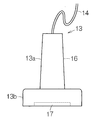
도 1은 본 발명의 일 실시 형태에 따른 전자 기기의 일 구체예, 즉 초음파 진단 장치(11)의 구성을 개략적으로 도시한다. 초음파 진단 장치(11)는 장치 단말기(12)와 초음파 프로브(프로브)(13)를 구비한다. 장치 단말기(12)와 초음파 프로브(13)는 케이블(14)로 서로 접속된다. 장치 단말기(12)와 초음파 프로브(13)는 케이블(14)을 통하여 전기 신호를 교환한다. 장치 단말기(12)에는 디스플레이 패널(표시 장치)(15)이 조립된다. 디스플레이 패널(15)의 화면은 장치 단말기(12)의 표면에서 노출된다. 장치 단말기(12)에서는, 후술되는 바와 같이, 초음파 프로브(13)에 의해 검출된 초음파에 기초하여 화상이 생성된다. 화상화된 검출 결과가 디스플레이 패널(15)의 화면에 표시된다.Fig. 1 schematically shows a configuration of an electronic device according to an embodiment of the present invention, that is, the configuration of the ultrasonic
도 2에 도시된 바와 같이, 초음파 프로브(13)는 케이스(16)를 갖는다. 케이스(16) 내에는 초음파 트랜스듀서 소자 칩(이하 「소자 칩」이라 함)(17)이 수용된다. 소자 칩(17)의 표면은 케이스(16)의 표면에서 노출될 수 있다. 소자 칩(17)은 표면으로부터 초음파를 출력하는 동시에 초음파의 반사파를 수신한다. 그 외, 초음파 프로브(13)는, 프로브 본체(13a)에 착탈 가능하게 연결되는 프로브 헤드(13b)를 구비할 수 있다. 이때, 소자 칩(17)은 프로브 헤드(13b)의 케이스(16) 내에 내장될 수 있다.As shown in FIG. 2, the
(2) 초음파 트랜스듀서 소자 칩의 구성(2) Configuration of Ultrasonic Transducer Element Chip
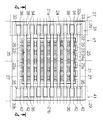
도 3은 일 실시 형태에 따른 소자 칩(17)의 평면도를 개략적으로 도시한다. 소자 칩(17)은 기판(21)을 구비한다. 기판(21)의 표면에는 소자 어레이(22)가 형성된다. 소자 어레이(22)는 초음파 트랜스듀서 소자(이하 「소자」라 함)(23)의 배열로 구성된다. 배열은 복수행 복수열의 매트릭스로 형성된다. 개개의 소자(23)는 압전 소자부를 구비한다. 압전 소자부는 하부 전극(24), 상부 전극(25) 및 압전체막(26)으로 구성된다. 개개의 소자(23)마다 하부 전극(24) 및 상부 전극(25)의 사이에 압전체막(26)이 끼워 넣어진다.3 schematically shows a plan view of an
하부 전극(24)은 복수개의 제1 도전체(24a)를 갖는다. 제1 도전체(24a)는 배열의 행방향으로 서로 평행하게 연장된다. 1행의 소자(23)마다 1개의 제1 도전체(24a)가 할당된다. 1개의 제1 도전체(24a)는 배열의 행방향으로 배열되는 소자(23)의 압전체막(26)에 공통으로 배치된다. 제1 도전체(24a)의 양단은 1쌍의 인출 배선(27)에 각각 접속된다. 인출 배선(27)은 배열의 열 방향으로 서로 평행하게 연장된다. 따라서, 모든 제1 도전체(24a)는 동일 길이를 갖는다. 이와 같이 하여 매트릭스 전체의 소자(23)에 공통적으로 하부 전극(24)은 접속된다.The
상부 전극(25)은 복수개의 제2 도전체(25a)를 갖는다. 제2 도전체(25a)는 배열의 열 방향으로 서로 평행하게 연장된다. 1열의 소자(23)마다 1개의 제2 도전체(25a)가 할당된다. 1개의 제2 도전체(25a)는 배열의 열 방향으로 배열되는 소자(23)의 압전체막(26)에 공통적으로 배치된다. 열마다 소자(23)의 통전은 절환된다. 이와 같은 통전의 절환에 따라 라인 스캔이나 섹터 스캔은 실현된다. 1열의 소자(23)는 동시에 초음파를 출력하는 점에서, 1열의 개수, 즉 배열의 행수는 초음파의 출력 레벨에 따라 결정될 수 있다. 행수는, 예를 들면 10∼15행 정도로 설정되면 된다. 도면에서는 생략되어 5행이 나타나 있다. 배열의 열수는 스캔의 범위의 넓이에 따라 결정될 수 있다. 열수는, 예를 들면 128열이나 256열로 설정되면 된다. 도면에서는 생략되어 8열이 나타나 있다. 그 외, 배열로는 지그재그 배치가 확립되어도 된다. 지그재그 배치에서는 짝수열의 소자(23)군은 홀수열의 소자(23)군에 대해 행 피치의 2분의 1로 어긋나게 되면 된다. 홀수열 및 짝수열의 한쪽의 소자수는 다른 쪽의 소자수에 비해 1개 적어도 된다. 또한, 하부 전극(24) 및 상부 전극(25)의 역할은 교체되어도 된다. 즉, 매트릭스 전체의 소자(23)에 공통적으로 상부 전극이 접속되는 한편, 배열의 열마다 공통적으로 소자(23)에 하부 전극이 접속되어도 된다.The
기판(21)의 외연은, 서로 평행한 1쌍의 직선(29)으로 구획되어 대향하는 제1 변(21a) 및 제2 변(21b)을 갖는다. 소자 어레이(22)의 윤곽과 기판(21)의 외연과의 사이에 넓어지는 주연 영역(31)에는, 제1 변(21a)과 소자 어레이(22)의 윤곽과의 사이에 1라인의 제1 단자 어레이(32a)가 배치되고, 제2 변(21b)과 소자 어레이(22)의 윤곽 사이에 1라인의 제2 단자 어레이(32b)가 배치된다. 제1 단자 어레이(32a)는 제1 변(21a)에 평행하게 1라인을 형성할 수 있다. 제2 단자 어레이(32b)는 제2 변(21b)에 평행하게 1라인을 형성할 수 있다. 제1 단자 어레이(32a)는 1쌍의 하부 전극 단자(33) 및 복수의 상부 전극 단자(34)로 구성된다. 마찬가지로, 제2 단자 어레이(32b)는 1쌍의 하부 전극 단자(35) 및 복수의 상부 전극 단자(36)로 구성된다. 1개의 인출 배선(27)의 양단에 각각 하부 전극 단자(33, 35)는 접속된다. 인출 배선(27) 및 하부 전극 단자(33, 35)는 소자 어레이(22)를 이등분하는 수직면에서 면대칭으로 형성되면 된다. 1개의 제2 도전체(25a)의 양단에 각각 상부 전극 단자(34, 36)는 접속된다. 제2 도전체(25a) 및 상부 전극 단자(34, 36)는 소자 어레이(22)를 이등분하는 수직면에서 면대칭으로 형성되면 된다.The outer edge of the board |
기판(21)에는 제1 플렉시블 프린트 기판(이하 「제1 플렉시블」이라 함)(37)이 연결된다. 제1 플렉시블(37)은 제1 단자 어레이(32a)에 덮인다. 제1 플렉시블(37)의 일단에는 하부 전극 단자(33) 및 상부 전극 단자(34)에 개별로 대응하여 도전선, 즉 제1 신호선(38)이 형성된다. 제1 신호선(38)은 하부 전극 단자(33) 및 상부 전극 단자(34)에 개별로 마주 보게 되어 개별로 접합된다. 마찬가지로, 기판(21)에는 제2 플렉시블 프린트 기판(이하 「제2 플렉시블」이라 함)(41)이 덮인다. 제2 플렉시블(41)은 제2 단자 어레이(32b)에 덮인다. 제2 플렉시블(41)의 제1 단부(41a)에는 하부 전극 단자(35) 및 상부 전극 단자(36)에 개별로 대응하여 도전선, 즉 제2 신호선(42)이 형성된다. 제2 신호선(42)은 하부 전극 단자(35) 및 상부 전극 단자(36)에 개별로 마주 보게 되어 개별로 접합된다.A first flexible printed circuit board (hereinafter referred to as "first flexible") 37 is connected to the
도 4에 도시된 바와 같이, 개개의 소자(23)는 진동막(43)을 갖는다. 진동막(43)의 구축에 있어서 기판(21)의 기체(44)에는 개개의 소자(23)마다 개구(45)가 형성된다. 개구(45)는 기체(44)에 대해 어레이 형상으로 배치된다. 기체(44)의 표면에는 가요막(46)이 일면에 형성된다. 가요막(46)은, 기체(44)의 표면에 적층되는 산화실리콘(SiO2)층(47)과, 산화실리콘층(47)의 표면에 적층되는 산화지르코늄(ZrO2)층(48)으로 구성된다. 가요막(46)은 개구(45)에 접한다. 이와 같이 하여 개구(45)의 윤곽에 대응하여 가요막(46)의 일부가 진동막(43)으로서 기능한다. 산화실리콘층(47)의 막 두께는 공진 주파수에 기초하여 결정될 수 있다.As shown in FIG. 4, the
진동막(43)의 표면에 하부 전극(24), 압전체막(26) 및 상부 전극(25)이 순서대로 적층된다. 하부 전극(24)에는, 예를 들면 티타늄(Ti), 이리듐(Ir), 백금(Pt) 및 티타늄(Ti)의 적층막이 이용될 수 있다. 압전체막(26)은, 예를 들면 지르콘산티탄산납(PZT)으로 형성될 수 있다. 상부 전극(25)은, 예를 들면 이리듐(Ir)으로 형성될 수 있다. 하부 전극(24) 및 상부 전극(25)에는 그 외의 도전재가 이용되어도 되고, 압전체막(26)에는 그 외의 압전 재료가 이용되어도 된다. 여기서는, 상부 전극(25) 아래에서 압전체막(26)은 완전하게 하부 전극(24)을 덮는다. 압전체막(26)의 작용으로 상부 전극(25)과 하부 전극(24)과의 사이에서 단락은 회피될 수 있다.The
기판(21)의 표면에는 보호막(49)이 적층된다. 보호막(49)은, 예를 들면 전체면에 걸쳐 기판(21)의 표면에 덮인다. 그 결과, 소자 어레이(22)나 제1 및 제2 단자 어레이(32a, 32b), 제1 및 제2 플렉시블(37, 41)의 제1 단부(37a, 41a)는 보호막(49)으로 덮인다. 보호막(49)에는, 예를 들면 실리콘 수지막이 이용될 수 있다. 보호막(49)은, 소자 어레이(22)의 구조나, 제1 단자 어레이(32a) 및 제1 플렉시블(37)의 접합, 제2 단자 어레이(32b) 및 제2 플렉시블(41)의 접합을 보호한다.The
매트릭스의 행 방향 및 열 방향에 인접하는 개구(45)끼리의 사이에는 구획벽(51)이 구획된다. 개구(45)끼리는 구획벽(51)으로 구획된다. 구획벽(51)의 벽 두께 t는 개구(45)의 공간끼리의 간격에 상당한다. 구획벽(51)은 서로 평행하게 넓어지는 평면 내에 2개의 벽면을 규정한다. 벽 두께 t는 벽면끼리의 거리에 상당한다. 즉, 벽 두께 t는 벽면에 직교하여 벽면끼리의 사이에 있는 수선의 길이로 규정될 수 있다. 구획벽(51)의 벽 높이 H는 개구(45)의 깊이에 상당한다. 개구(45)의 깊이는 기체(44)의 두께에 상당한다. 따라서, 구획벽(51)의 벽 높이 H는 기체(44)의 두께 방향으로 규정되는 벽면의 길이로 규정될 수 있다. 기체(44)는 균일한 두께를 가지므로, 구획벽(51)은 전체 길이에 걸쳐 일정한 벽 높이 H를 가질 수 있다. 구획벽(51)의 벽 두께 t가 축소되면, 진동막(43)의 배치 밀도는 높아진다. 소자 칩(17)의 소형화에 기여할 수 있다. 벽 두께 t에 비해 구획벽(51)의 벽 높이 H가 크면, 소자 칩(17)의 굽힘 강성은 높아질 수 있다. 이와 같이 하여 개구(45)끼리의 간격은 개구(45)의 깊이보다도 작게 설정된다.The
기체(44)의 이면에는 보강판(판 형상 부재)(52)이 고정된다. 보강판(52)의 표면에 기체(44)의 이면이 겹쳐진다. 보강판(52)의 표면은 가상 평면 HP 내에서 넓어진다. 기체(44)의 이면도 가상 평면 HP 내에서 넓어지는 점에서, 기체(44)의 이면은 최대한 넓은 면적에서 보강판(52)의 표면에 접할 수 있다. 보강판(52)은 소자 칩(17)의 이면에서 개구(45)를 폐쇄한다. 보강판(52)은 기체(44)의 두께 방향으로부터의 평면에서 보아 개구(45)를 덮는다. 보강판(52)은 리지드(rigid)한 기재를 구비할 수 있다. 보강판(52)은, 예를 들면 실리콘 기판으로 형성될 수 있다. 기체(44)의 판 두께는, 예를 들면 100㎛ 정도로 설정되고, 보강판(52)의 판 두께는, 예를 들면 100∼150㎛ 정도로 설정된다. 여기서는, 구획벽(51)은 보강판(52)에 결합된다. 보강판(52)은 개개의 구획벽(51)에 적어도 1개소의 접합 영역에서 접합된다. 접합에 있어서 접착제는 이용될 수 있다.The reinforcing plate (plate-shaped member) 52 is fixed to the back surface of the
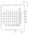
도 5에 도시된 바와 같이, 개구(45)는 제1 방향 D1로 열을 형성한다. 개구(45)의 윤곽 형상의 도형 중심(55)은 제1 방향 D1의 1직선(56) 상에서 등 피치로 배치된다. 개구(45)는 1개의 윤곽 형상의 복사로 본떠지는 점에서, 동일 형상의 개구(45)가 일정한 피치로 반복 배치된다. 개구(45)의 윤곽(45a)은, 예를 들면 사각형으로 규정된다. 구체적으로는 사각형으로 형성된다. 사각형의 긴 변은 제1 방향 D1에 맞추어진다. 이와 같이 하여 개구(45)는 사각형의 윤곽(45a)을 가지므로, 구획벽(51)은 전체 길이에 걸쳐 일정한 벽 두께 t를 가질 수 있다. 이때, 구획벽(51)의 접합 영역은 긴 변의 중앙 위치를 포함하는 영역이면 된다. 특히, 구획벽(51)의 접합 영역은 긴 변의 전체 길이를 포함하는 영역이면 된다. 구획벽(51)은 긴 변의 전체 길이에 걸쳐 개구(45)끼리의 사이의 전체면에서 보강판(52)에 면접합될 수 있다. 또한, 구획벽(51)의 접합 영역은 사각형의 각 변에 적어도 1개소씩 배치될 수 있다. 구획벽(51)의 접합 영역은 사각형을 도중에 끊기는 일 없이 둘러쌀 수 있다. 구획벽(51)은 사각형의 전체 둘레에 걸쳐 개구(45)끼리의 사이의 전체면에서 보강판(52)에 면접합될 수 있다.As shown in FIG. 5, the
(3) 초음파 진단 장치의 회로 구성(3) Circuit configuration of the ultrasonic diagnostic device
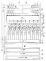
도 6에 도시된 바와 같이, 집적 회로는 멀티플렉서(61) 및 송수신 회로(62)를 구비한다. 멀티플렉서(61)는 소자 칩(17)측의 포트군(61a)과 송수신 회로(62)측의 포트군(61b)을 구비한다. 소자 칩(17)측의 포트군(61a)에는 제1 배선(54) 경유로 제1 신호선(38) 및 제2 신호선(42)이 접속된다. 이와 같이 하여 포트군(61a)은 소자 어레이(22)에 연결된다. 여기서는, 송수신 회로(62)측의 포트군(61b)에는 집적 회로 칩(55) 내의 규정수의 신호선(63)이 접속된다. 규정수는 스캔에 있어서 동시에 출력되는 소자(23)의 열수에 상당한다. 멀티플렉서(61)는 케이블(14)측의 포트와 소자 칩(17)측의 포트와의 사이에서 상호 접속을 관리한다.As shown in FIG. 6, the integrated circuit includes a
송수신 회로(62)는 규정수의 절환 스위치(64)를 구비한다. 개개의 절환 스위치(64)는 각각 개별로 대응의 신호선(63)에 접속된다. 송수신 회로(62)는 개개의 절환 스위치(64)마다 송신 경로(65) 및 수신 경로(66)를 구비한다. 절환 스위치(64)에는 송신 경로(65)와 수신 경로(66)가 병렬로 접속된다. 절환 스위치(64)는 멀티플렉서(61)에 선택적으로 송신 경로(65) 또는 수신 경로(66)를 접속한다. 송신 경로(65)에는 펄서(pulser; 67)가 내장된다. 펄서(67)는 진동막(52)의 공진 주파수에 따른 주파수로 펄스 신호를 출력한다. 수신 경로(66)에는 앰프(68), 로우 패스 필터(LPF)(69) 및 아날로그 디지털 변환기(ADC)(71)가 내장된다. 개개의 소자(23)의 검출 신호는 증폭되어 디지털 신호로 변환된다.The transmission /
송수신 회로(62)는 구동/수신 회로(72)를 구비한다. 송신 경로(65) 및 수신 경로(66)는 구동/수신 회로(72)에 접속된다. 구동/수신 회로(72)는 스캔의 형태에 따라 동시에 펄서(67)를 제어한다. 구동/수신 회로(72)는 스캔의 형태에 따라 검출 신호의 디지털 신호를 수신한다. 구동/수신 회로(72)는 제어선(73)으로 멀티플렉서(61)에 접속된다. 멀티플렉서(61)는 구동/수신 회로(72)로부터 공급되는 제어 신호에 기초하여 상호 접속의 관리를 실시한다.The transmit / receive
장치 단말기(12)에는 처리 회로(74)가 내장된다. 처리 회로(74)는, 예를 들면 중앙 연산 처리 장치(CPU)나 메모리를 구비할 수 있다. 초음파 진단 장치(11)의 전체 동작은 처리 회로(74)의 처리에 따라서 제어된다. 유저로부터 입력되는 지시에 따라 처리 회로(74)는 구동/수신 회로(72)를 제어한다. 처리 회로(74)는 소자(23)의 검출 신호에 따라 화상을 생성한다. 화상은 묘화 데이터로 특정된다.The
장치 단말기(12)에는 묘화 회로(75)가 내장된다. 묘화 회로(75)는 처리 회로(74)에 접속된다. 묘화 회로(75)에는 디스플레이 패널(15)이 접속된다. 묘화 회로(75)는 처리 회로(74)에서 생성된 묘화 데이터에 따라 구동 신호를 생성한다. 구동 신호는 디스플레이 패널(15)에 보내진다. 그 결과, 디스플레이 패널(15)에 화상이 투영된다.The drawing
(4) 초음파 진단 장치의 동작(4) operation of the ultrasonic diagnostic apparatus
다음으로 초음파 진단 장치(11)의 동작을 간단히 설명한다. 처리 회로(74)는 구동/수신 회로(72)에 초음파의 송신 및 수신을 지시한다. 구동/수신 회로(72)는 멀티플렉서(61)에 제어 신호를 공급함과 함께 개개의 펄서(67)에 구동 신호를 공급한다. 펄서(67)는 구동 신호의 공급에 따라 펄스 신호를 출력한다. 멀티플렉서(61)는 제어 신호의 지시에 따라서 포트군(61b)의 포트에 포트군(61a)의 포트를 접속한다. 펄스 신호는 포트의 선택에 따라 하부 전극 단자(33, 35) 및 상부 전극 단자(34, 36)를 통하여 열마다 소자(23)에 공급된다. 펄스 신호의 공급에 따라 진동막(43)은 진동한다. 그 결과, 대상물(예를 들면, 인체의 내부)을 향해 원하는 초음파는 발하게 된다.Next, the operation of the ultrasonic
초음파의 송신 후, 절환 스위치(64)는 절환된다. 멀티플렉서(61)는 포트의 접속 관계를 유지한다. 절환 스위치(64)는 송신 경로(65) 및 신호선(63)의 접속 대신에 수신 경로(66) 및 신호선(63)의 접속을 확립한다. 초음파의 반사파는 진동막(43)을 진동시킨다. 그 결과, 소자(23)로부터 검출 신호가 출력된다. 검출 신호는 디지털 신호로 변환되어 구동/수신 회로(72)에 보내진다.After transmission of the ultrasonic waves, the change-
초음파의 송신 및 수신은 반복된다. 반복에 있어서 멀티플렉서(61)는 포트의 접속 관계를 변경한다. 그 결과, 라인 스캔이나 섹터 스캔은 실현된다. 스캔이 완료되면, 처리 회로(74)는 검출 신호의 디지털 신호에 기초하여 화상을 형성한다. 형성된 화상은 디스플레이 패널(15)의 화면에 표시된다.The transmission and reception of the ultrasound is repeated. In repetition, the
소자 칩(17)에서는 소자(23)는 박형으로 형성될 수 있다. 소자(23)는 박형의 기판(21)에 형성될 수 있다. 보강판(52)이 기판(21)에 고정되어도, 소자 칩(17)은 박형으로 형성될 수 있다. 동시에, 보강판(52)은 기판(21)의 강도를 보강한다. 특히, 구획벽(51)에서 벽 두께 t가 벽 높이 H보다도 작다는 점에서, 단면계수의 관계상 구획벽(51)에서는 기판(21)의 두께 방향으로 충분한 강성이 확보될 수 있다. 기판(21)의 두께 방향의 힘은 구획벽(51)을 타고 보강판(52)에 의해 지지될 수 있다. 이와 같이 하여 소자 칩(17)은 기판(21)의 두께 방향으로 충분한 강도를 가질 수 있다. 그리고, 기판(21)의 판 두께가, 예를 들면 100㎛ 정도로 설정되어도, 보강판(52)은 기판(21)의 파손을 방지할 수 있다. 한편, 벌크형의 초음파 트랜스듀서 소자로 소자 어레이가 구성되는 경우에는, 기판의 판 두께는 수㎜ 정도로 설정된다. 가령 보강판(52)이 접합되어도, 본 실시 형태에 따른 소자 칩(17)의 두께는, 벌크형의 초음파 트랜스듀서 소자로 소자 어레이가 구성되는 경우에 비해 확실하게 축소될 수 있다. 더하여, 진동막(43)의 음향 임피던스는 벌크형의 초음파 트랜스듀서 소자에 비해 인체의 그것에 가까운 점에서, 소자 칩(17)에서는 벌크형의 초음파 트랜스듀서 소자에 비해 음향 임피던스의 정합층이 생략될 수 있다. 이러한 정합층의 생략은 소자 칩(17)의 박형화에 더욱 기여할 수 있다.In the
보강판(52)은 개개의 구획벽(51)에 적어도 1개소의 접합 영역에서 접합된다. 구획벽(51)이 보강판(52)에 접합되면, 구획벽(51)의 작용은 보강판(52)에 의해 구속된다. 따라서, 구획벽(51)의 진동은 방지될 수 있다. 그 결과, 소자(23)끼리의 크로스토크는 방지될 수 있다. 또한, 이와 같이 하여 구획벽(51)의 작용이 구속되면, 소자(23)의 초음파 진동에 대해 구획벽(51)의 진동의 작용은 회피될 수 있다. 소자(23)에서는 클리어한 진동 모드의 초음파 진동이 얻어진다. 이와 같이 하여 구획벽(51)의 진동이 회피되면, 초음파 진동의 진폭의 저하도 억제될 수 있다. 한편, 구획벽(51)이 작용하면, 진동막(43)의 상하 진동 모드보다도 낮은 주파수의 왜곡된 진동 모드가 나타난다. 또한, 구획벽(51)이 작용하는 분만큼 진동막(43)의 운동 에너지가 감소하고 진동의 진폭이 저하되어 버린다.The
사각형 윤곽끼리의 개구(45)가 인접하면, 구획벽(51)은 균일한 벽 두께 t로 형성될 수 있다. 따라서, 소자(23)의 밀집도는 높아질 수 있다. 이와 같이 하여 소자(23)의 밀집도가 높아지면 높아질수록, 구획벽(51)의 벽 두께 t는 균일하게 감소한다. 따라서, 구획벽(51)의 강성은 현저하게 약해진다. 이와 같은 때에 구획벽(51)이 보강판(52)에 연결되면, 구획벽(51)의 진동은 효과적으로 방지될 수 있다.When the
구획벽(51)의 접합 영역은 긴 변의 중앙 위치를 포함하는 영역일 수 있다. 구획벽(51) 중 진동 진폭이 큰 부위가 보강판(52)에 접합된다. 그 결과, 구획벽(51)의 진동은 효과적으로 방지될 수 있다. 또한, 구획벽(51)의 접합 영역은 긴 변의 전체 길이를 포함하는 영역일 수 있다. 이와 같이 하여 긴 변의 전체 길이에 걸쳐 구획벽(51)이 보강판(52)에 접합되면, 구획벽(51)의 진동은 확실하게 방지될 수 있다. 또한, 구획벽(51)은 긴 변의 전체 길이에 걸쳐 개구(45)끼리의 사이의 전체면에서 면접합될 수 있다. 이와 같이 하여 긴 변의 전체 길이에 걸쳐 개구(45)끼리의 사이에서 전체면에서 구획벽(51)이 보강판(52)에 면접합되면, 구획벽(51)의 진동은 확실하게 방지될 수 있다.The junction area of the
구획벽(51)의 접합 영역은 사각형의 각 변에 적어도 1개소씩 배치되면 된다. 이와 같이 하여 사각형의 각 변에서 구획벽(51)이 보강판(52)에 접합되면, 구획벽(51)의 진동은 확실하게 방지될 수 있다. 또한, 구획벽(51)의 접합 영역은 사각형을 도중에 끊기는 일 없이 둘러쌀 수 있다. 이와 같이 하여 사각형의 전역에서 구획벽(51)이 보강판(52)에 접합되면, 구획벽(51)의 진동은 확실하게 방지될 수 있다. 게다가, 구획벽(51)은 사각형의 전체 둘레에 걸쳐 개구(45)끼리의 사이의 전체면에서 면접합될 수 있다. 이와 같이 하여 사각형의 전체 둘레에 걸쳐 개구(45)끼리의 사이에서 전체면에서 구획벽(51)이 보강판(52)에 면접합되면, 구획벽(51)의 진동은 확실하게 방지될 수 있다.The joining region of the
(5) 초음파 트랜스듀서 소자 칩의 제조 방법(5) Manufacturing method of ultrasonic transducer element chip
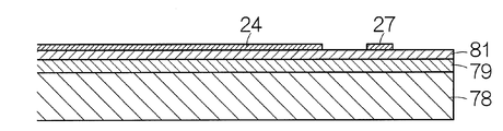
도 7에 도시된 바와 같이, 실리콘 웨이퍼(78)의 표면에서 개개의 소자 칩(17)마다 하부 전극(24), 인출 배선(27) 및 하부 전극 단자(33, 35)(도 7 이후에서는 도시되지 않음)가 형성된다. 하부 전극(24), 인출 배선(27) 및 하부 전극 단자(33, 35)의 형성에 앞서 실리콘 웨이퍼(78)의 표면에는 산화실리콘막(79) 및 산화지르코늄막(81)이 잇달아 형성된다. 산화지르코늄막(81)의 표면에는 도전막이 형성된다. 도전막은 티타늄, 이리듐, 백금 및 티타늄의 적층막으로 구성된다. 포토리소그래피 기술에 기초하여 도전막으로부터 하부 전극(24), 인출 배선(27) 및 하부 전극 단자(33, 35)는 성형된다.As shown in FIG. 7, the
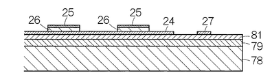
도 8에 도시된 바와 같이, 하부 전극(24)의 표면에서 개개의 소자(23)마다 압전체막(26) 및 상부 전극(25)이 형성된다. 압전체막(26) 및 상부 전극(25)의 형성에 있어서 실리콘 웨이퍼(78)의 표면에는 압전 재료막 및 도전막이 성막된다. 압전 재료막은 PZT막으로 구성된다. 도전막은 이리듐막으로 구성된다. 포토리소그래피 기술에 기초하여 개개의 소자(23)마다 압전 재료막 및 도전막으로 압전체막(26) 및 상부 전극(25)이 성형된다.As shown in FIG. 8, a
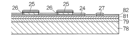
계속해서, 도 9에 도시된 바와 같이, 실리콘 웨이퍼(78)의 표면에 도전막(82)이 성막된다. 도전막(82)은 개개의 소자 칩(17) 내에서 열마다에 상부 전극(25)을 서로 접속한다. 그리고, 포토리소그래피 기술에 기초하여 도전막(82)으로부터 상부 전극(25) 및 상부 전극 단자(34, 36)가 성형된다.Subsequently, as shown in FIG. 9, a
그 후, 도 10에 도시된 바와 같이, 실리콘 웨이퍼(78)의 이면으로부터 어레이 형상의 개구(45)가 형성된다. 개구(45)의 형성에 있어서 에칭 처리가 실시된다. 산화실리콘막(79)은 에칭 스톱층으로서 기능한다. 산화실리콘막(79) 및 산화지르코늄막(81)에 진동막(43)은 구획된다. 개구(45)의 형성 후, 실리콘 웨이퍼(78)의 이면에 보강판용의 웨이퍼(83)의 표면이 서로 겹쳐진다. 웨이퍼(83)에는, 예를 들면 리지드한 절연성 기판이 이용될 수 있다. 절연성 기판에는 실리콘 웨이퍼가 이용될 수 있다. 접합에 있어서, 예를 들면 접착제가 이용될 수 있다. 접합 후, 실리콘 웨이퍼(78)로부터 개개의 소자 칩(17)은 잘라내어진다.Thereafter, as shown in FIG. 10, an array-shaped
또한, 상기한 바와 같이 본 실시 형태에 대해 상세하게 설명하였지만, 본 발명의 신규 사항 및 효과로부터 실체적으로 일탈하지 않는 많은 변형이 가능한 것은 당업자는 용이하게 이해할 수 있을 것이다. 따라서, 이와 같은 변형예는 전부 본 발명의 범위에 포함된다. 예를 들면, 명세서 또는 도면에 있어서, 적어도 한번, 보다 광의 또는 동의의 상이한 용어와 함께 기재된 용어는, 명세서 또는 도면의 어떠한 개소에 있어서도, 그 상이한 용어로 치환할 수 있다. 또한, 초음파 진단 장치(11), 초음파 프로브(13), 소자 칩(17), 소자(23) 등의 구성 및 동작도 본 실시 형태에서 설명한 것으로 한정되지 않고, 다양한 변형이 가능하다.In addition, although the present embodiment has been described in detail as described above, those skilled in the art will readily appreciate that many modifications are possible without departing substantially from the novelty and effects of the present invention. Therefore, all such modifications are included in the scope of the present invention. For example, in a specification or drawing, the term described with the different terms of broader or more synonymous at least once may be substituted by the different terminus in any part of a specification or drawing. In addition, the structure and operation | movement of the ultrasonic
11 : 전자 기기(초음파 진단 장치)
13 : 프로브(초음파 프로브)
13b : 프로브 헤드
15 : 표시 장치(디스플레이 패널)
16 : 케이스
17 : 초음파 트랜스듀서 소자 칩
21 : 기판
23 : 초음파 트랜스듀서 소자
45 : 개구
51 : 구획 벽부(구획벽)
52 : 판 형상 부재(보강판)11: electronic device (ultrasonic diagnostic device)
13: probe (ultrasonic probe)
13b: probe head
15: display device (display panel)
16: Case
17: ultrasonic transducer element chip
21: substrate
23: ultrasonic transducer element
45: opening
51: partition wall (compartment wall)
52: plate-shaped member (reinforcement plate)
Claims (13)
개개의 상기 복수의 개구에 설치되는 초음파 트랜스듀서 소자와,
상기 기판의 상기 초음파 트랜스듀서 소자가 설치되는 면과는 반대측의 면에 고정되며, 상기 기판의 두께 방향으로부터의 평면에서 보아 상기 복수의 개구 중 적어도 1개 이상을 덮는 판 형상 부재
를 구비하고,
상기 복수의 개구의 사이의 구획 벽부에서는, 벽 두께가 벽 높이보다 작은 것을 특징으로 하는 초음파 트랜스듀서 소자 칩.A substrate having a plurality of openings arranged in an array shape;
An ultrasonic transducer element provided in each of said plurality of openings;
The plate-shaped member which is fixed to the surface on the opposite side to the surface in which the said ultrasonic transducer element of the said board | substrate is installed, and covers at least 1 or more of the said some opening in plan view from the thickness direction of the said board | substrate.
And,
An ultrasonic transducer element chip, characterized in that the wall thickness is smaller than the wall height in the partition wall portion between the plurality of openings.
상기 판 형상 부재는 개개의 상기 구획 벽부에 적어도 1개소의 접합 영역에서 접합되는 것을 특징으로 하는 초음파 트랜스듀서 소자 칩.The method of claim 1,
The plate-shaped member is bonded to at least one joining region of each of the partition wall portions. An ultrasonic transducer element chip.
상기 개구의 윤곽은 사각형으로 규정되는 것을 특징으로 하는 초음파 트랜스듀서 소자 칩.3. The method according to claim 1 or 2,
And the contour of the opening is defined by a square.
상기 사각형은 대향하는 2변의 긴 변을 가지며, 상기 구획 벽부의 상기 접합 영역은 상기 긴 변의 중앙 위치를 포함하는 영역인 것을 특징으로 하는 초음파 트랜스듀서 소자 칩.The method of claim 3,
The quadrangle has two opposite sides of the long side, and the joining area of the partition wall is an area including a central position of the long side.
상기 구획 벽부의 상기 접합 영역은 상기 긴 변의 전체 길이를 포함하는 영역인 것을 특징으로 하는 초음파 트랜스듀서 소자 칩.5. The method of claim 4,
And the joining region of the partition wall portion is an area including the entire length of the long side.
상기 구획 벽부는 상기 긴 변의 전체 길이에 걸쳐 상기 개구끼리의 사이의 전체면에서 면접합되는 것을 특징으로 하는 초음파 트랜스듀서 소자 칩.The method of claim 5,
And the partition wall portion is bonded to the entire surface between the openings over the entire length of the long side.
상기 구획 벽부의 상기 접합 영역은 상기 사각형의 각 변에 적어도 1개소씩 배치되는 것을 특징으로 하는 초음파 트랜스듀서 소자 칩.The method of claim 3,
And the joining region of the partition wall portion is disposed at least at each side of the quadrangle.
상기 구획 벽부의 상기 접합 영역은 상기 사각형을 도중에서 끊김없이 둘러싸는 것을 특징으로 하는 초음파 트랜스듀서 소자 칩.The method of claim 7, wherein
And the joining region of the partition wall portion surrounds the quadrilateral seamlessly.
상기 구획 벽부는 상기 사각형의 전체 둘레에 걸쳐 상기 개구끼리의 사이의 전체면에서 면접합되는 것을 특징으로 하는 초음파 트랜스듀서 소자 칩.9. The method of claim 8,
And the partition wall portion is bonded to the entire surface between the openings over the entire circumference of the quadrangle.
상기 초음파 트랜스듀서 소자 칩을 지지하는 케이스
를 구비하는 것을 특징으로 하는 프로브 헤드.The ultrasonic transducer element chip of any one of Claims 1-9,
A case supporting the ultrasonic transducer element chip
Wherein the probe head is made of a metal.
Applications Claiming Priority (2)
| Application Number | Priority Date | Filing Date | Title |
|---|---|---|---|
| JP2012038402A JP5990930B2 (en) | 2012-02-24 | 2012-02-24 | Ultrasonic transducer element chip and probe, electronic device and ultrasonic diagnostic apparatus |
| JPJP-P-2012-038402 | 2012-02-24 |
Publications (1)
| Publication Number | Publication Date |
|---|---|
| KR20130097655A true KR20130097655A (en) | 2013-09-03 |
Family
ID=49002733
Family Applications (1)
| Application Number | Title | Priority Date | Filing Date |
|---|---|---|---|
| KR1020130015736A KR20130097655A (en) | 2012-02-24 | 2013-02-14 | Ultrasonic transducer element chip, probe, electronic instrument, and ultrasonic diagnostic device |
Country Status (5)
| Country | Link |
|---|---|
| US (3) | US9099635B2 (en) |
| JP (1) | JP5990930B2 (en) |
| KR (1) | KR20130097655A (en) |
| CN (2) | CN103286056B (en) |
| TW (1) | TWI599237B (en) |
Families Citing this family (26)
| Publication number | Priority date | Publication date | Assignee | Title |
|---|---|---|---|---|
| JP5990930B2 (en) * | 2012-02-24 | 2016-09-14 | セイコーエプソン株式会社 | Ultrasonic transducer element chip and probe, electronic device and ultrasonic diagnostic apparatus |
| JP6102075B2 (en) | 2012-03-30 | 2017-03-29 | セイコーエプソン株式会社 | Ultrasonic transducer element chip and probe, electronic device and ultrasonic diagnostic apparatus |
| JP5900107B2 (en) * | 2012-03-30 | 2016-04-06 | セイコーエプソン株式会社 | Ultrasonic transducer element chip and probe, electronic device and ultrasonic diagnostic apparatus |
| JP6175780B2 (en) * | 2013-01-28 | 2017-08-09 | セイコーエプソン株式会社 | Ultrasonic device, ultrasonic probe, electronic device and ultrasonic imaging apparatus |
| JP6206033B2 (en) * | 2013-09-24 | 2017-10-04 | セイコーエプソン株式会社 | Ultrasonic transducer device and ultrasonic measurement apparatus |
| JP6442821B2 (en) * | 2013-09-30 | 2018-12-26 | セイコーエプソン株式会社 | Ultrasonic device and electronic equipment |
| JP6229431B2 (en) * | 2013-10-28 | 2017-11-15 | セイコーエプソン株式会社 | Ultrasonic device, ultrasonic probe head, ultrasonic probe, electronic device and ultrasonic imaging apparatus |
| JP2015097733A (en) * | 2013-11-20 | 2015-05-28 | セイコーエプソン株式会社 | Ultrasound device and method of producing the same and electronic apparatus and ultrasonic image device |
| JP6281262B2 (en) * | 2013-11-29 | 2018-02-21 | セイコーエプソン株式会社 | Ultrasonic device and probe, electronic apparatus and ultrasonic imaging apparatus |
| JP6326833B2 (en) * | 2014-01-31 | 2018-05-23 | セイコーエプソン株式会社 | Ultrasonic device, method for manufacturing ultrasonic device, probe, electronic device, ultrasonic imaging apparatus |
| CN106664494A (en) * | 2014-07-04 | 2017-05-10 | 精工爱普生株式会社 | Ultrasonic sensor |
| JP6299511B2 (en) * | 2014-07-31 | 2018-03-28 | セイコーエプソン株式会社 | Ultrasonic device and probe and electronic equipment |
| JP2016033970A (en) | 2014-07-31 | 2016-03-10 | セイコーエプソン株式会社 | Ultrasonic device and method for manufacturing the same, and probe and electronic equipment |
| JP6402983B2 (en) * | 2014-08-29 | 2018-10-10 | セイコーエプソン株式会社 | Ultrasonic device, method for manufacturing ultrasonic device, ultrasonic probe, ultrasonic measuring device, electronic equipment |
| JP6314777B2 (en) * | 2014-09-30 | 2018-04-25 | セイコーエプソン株式会社 | Ultrasonic sensor and probe and electronic equipment |
| JP6536792B2 (en) * | 2015-03-25 | 2019-07-03 | セイコーエプソン株式会社 | Ultrasonic sensor and method of manufacturing the same |
| JP6610058B2 (en) * | 2015-07-29 | 2019-11-27 | セイコーエプソン株式会社 | Ultrasonic device and electronic equipment |
| JP2017046811A (en) * | 2015-08-31 | 2017-03-09 | セイコーエプソン株式会社 | Ultrasonic device, ultrasonic module, and ultrasonic measuring apparatus |
| JP6610883B2 (en) | 2015-12-17 | 2019-11-27 | セイコーエプソン株式会社 | Piezoelectric devices for ultrasonic sensors |
| JP6693154B2 (en) * | 2016-02-04 | 2020-05-13 | セイコーエプソン株式会社 | Ultrasonic transducer, ultrasonic probe, ultrasonic device, method of manufacturing ultrasonic transducer, and vibration device |
| JP2018129402A (en) | 2017-02-08 | 2018-08-16 | セイコーエプソン株式会社 | Piezoelectric element and manufacturing method therefor |
| CN109087999A (en) * | 2018-08-22 | 2018-12-25 | 京东方科技集团股份有限公司 | Flexible substrates and preparation method thereof, flexible organic light-emitting diode display substrate |
| WO2020188866A1 (en) * | 2019-03-18 | 2020-09-24 | 株式会社村田製作所 | Piezoelectric device |
| JP1650087S (en) * | 2019-05-23 | 2020-01-20 | ||
| USD941168S1 (en) * | 2019-10-22 | 2022-01-18 | Kabushiki Kaisha Toshiba | Vibration sensor |
| JP2022117116A (en) * | 2021-01-29 | 2022-08-10 | 株式会社ディスコ | Peeling device |
Citations (4)
| Publication number | Priority date | Publication date | Assignee | Title |
|---|---|---|---|---|
| JP2005051687A (en) * | 2003-07-31 | 2005-02-24 | Matsushita Electric Works Ltd | Piezoelectric ultrasonic sensor and resonance frequency adjustment method thereof |
| JP2008535643A (en) * | 2005-03-02 | 2008-09-04 | リサーチ・トライアングル・インスティチュート | Piezoelectric micromachined ultrasonic transducer with cavity supported by air |
| KR20100137842A (en) * | 2009-06-23 | 2010-12-31 | (주)메디슨 | Transducer for ultrasonic diagnosis device and method for manufaturing the same |
| KR20110129813A (en) * | 2010-05-26 | 2011-12-02 | 가부시끼가이샤 도시바 | Ultrasound probe and method of manufactureing the same |
Family Cites Families (21)
| Publication number | Priority date | Publication date | Assignee | Title |
|---|---|---|---|---|
| JP2794720B2 (en) * | 1988-08-23 | 1998-09-10 | 松下電器産業株式会社 | Composite piezoelectric vibrator |
| JP2000233158A (en) * | 1999-02-12 | 2000-08-29 | Omron Corp | Spraying device |
| TW449486B (en) * | 2000-07-24 | 2001-08-11 | Ind Tech Res Inst | Composite ultrasonic therapeutic energy converter and method for making the same |
| EP1671589A4 (en) * | 2003-10-02 | 2009-07-15 | Hitachi Medical Corp | Ultrasonic probe, ultrasonogrphic device, and ultrasonographic method |
| JP4575108B2 (en) * | 2004-10-15 | 2010-11-04 | 株式会社東芝 | Ultrasonic probe |
| WO2006121034A1 (en) * | 2005-05-09 | 2006-11-16 | Hitachi Medical Corporation | Ultrasonograph |
| EP1912748B1 (en) * | 2005-08-05 | 2015-07-08 | Koninklijke Philips N.V. | Curved two-dimensional array transducer |
| US8279712B2 (en) * | 2007-11-06 | 2012-10-02 | Akrion Systems Llc | Composite transducer apparatus and system for processing a substrate and method of constructing the same |
| WO2010044312A1 (en) * | 2008-10-17 | 2010-04-22 | コニカミノルタエムジー株式会社 | Array-type ultrasonic vibrator |
| FR2940579B1 (en) * | 2008-12-23 | 2012-09-28 | Ixsea | ACOUSTIC WAVE TRANSDUCER AND SONAR ANTENNA OF ENHANCED DIRECTIVITY. |
| JP5434109B2 (en) | 2009-02-06 | 2014-03-05 | セイコーエプソン株式会社 | Ultrasonic sensor unit |
| JP5310119B2 (en) | 2009-03-06 | 2013-10-09 | セイコーエプソン株式会社 | Ultrasonic sensor unit |
| JP2010233609A (en) * | 2009-03-30 | 2010-10-21 | Fujifilm Corp | Ultrasonic diagnostic apparatus and method of determining contact state |
| JP4947115B2 (en) | 2009-09-30 | 2012-06-06 | 株式会社村田製作所 | Ultrasonic transducer |
| JP2011082624A (en) | 2009-10-02 | 2011-04-21 | Asahi Kasei Electronics Co Ltd | Proximity ultrasonic sensor |
| JP5671876B2 (en) | 2009-11-16 | 2015-02-18 | セイコーエプソン株式会社 | Ultrasonic transducer, ultrasonic sensor, method for manufacturing ultrasonic transducer, and method for manufacturing ultrasonic sensor |
| CN102933318A (en) * | 2010-01-29 | 2013-02-13 | 三角形研究学会 | Methods for forming piezoelectric ultrasonic transducers, and associated apparatuses |
| CN202037116U (en) * | 2011-05-05 | 2011-11-16 | 重庆市伟岸测器制造股份有限公司 | Ultrasonic transducer |
| JP5990930B2 (en) * | 2012-02-24 | 2016-09-14 | セイコーエプソン株式会社 | Ultrasonic transducer element chip and probe, electronic device and ultrasonic diagnostic apparatus |
| JP6102075B2 (en) * | 2012-03-30 | 2017-03-29 | セイコーエプソン株式会社 | Ultrasonic transducer element chip and probe, electronic device and ultrasonic diagnostic apparatus |
| JP5900107B2 (en) * | 2012-03-30 | 2016-04-06 | セイコーエプソン株式会社 | Ultrasonic transducer element chip and probe, electronic device and ultrasonic diagnostic apparatus |
-
2012
- 2012-02-24 JP JP2012038402A patent/JP5990930B2/en active Active
-
2013
- 2013-02-14 KR KR1020130015736A patent/KR20130097655A/en not_active Application Discontinuation
- 2013-02-17 CN CN201310053151.9A patent/CN103286056B/en active Active
- 2013-02-17 CN CN201710088584.6A patent/CN106964531B/en active Active
- 2013-02-19 US US13/770,115 patent/US9099635B2/en active Active
- 2013-02-19 TW TW102105767A patent/TWI599237B/en active
-
2015
- 2015-06-29 US US14/753,121 patent/US9592534B2/en active Active
-
2017
- 2017-01-27 US US15/417,799 patent/US20170136497A1/en not_active Abandoned
Patent Citations (4)
| Publication number | Priority date | Publication date | Assignee | Title |
|---|---|---|---|---|
| JP2005051687A (en) * | 2003-07-31 | 2005-02-24 | Matsushita Electric Works Ltd | Piezoelectric ultrasonic sensor and resonance frequency adjustment method thereof |
| JP2008535643A (en) * | 2005-03-02 | 2008-09-04 | リサーチ・トライアングル・インスティチュート | Piezoelectric micromachined ultrasonic transducer with cavity supported by air |
| KR20100137842A (en) * | 2009-06-23 | 2010-12-31 | (주)메디슨 | Transducer for ultrasonic diagnosis device and method for manufaturing the same |
| KR20110129813A (en) * | 2010-05-26 | 2011-12-02 | 가부시끼가이샤 도시바 | Ultrasound probe and method of manufactureing the same |
Non-Patent Citations (1)
| Title |
|---|
| 일본 공표특허공보 특표2008-535643호(2008.09.04.) 1부. * |
Also Published As
| Publication number | Publication date |
|---|---|
| US20150298172A1 (en) | 2015-10-22 |
| US20130223191A1 (en) | 2013-08-29 |
| JP2013175879A (en) | 2013-09-05 |
| CN106964531A (en) | 2017-07-21 |
| TW201336325A (en) | 2013-09-01 |
| US20170136497A1 (en) | 2017-05-18 |
| CN103286056A (en) | 2013-09-11 |
| CN106964531B (en) | 2019-07-09 |
| CN103286056B (en) | 2017-03-01 |
| TWI599237B (en) | 2017-09-11 |
| US9592534B2 (en) | 2017-03-14 |
| US9099635B2 (en) | 2015-08-04 |
| JP5990930B2 (en) | 2016-09-14 |
Similar Documents
| Publication | Publication Date | Title |
|---|---|---|
| JP5990930B2 (en) | Ultrasonic transducer element chip and probe, electronic device and ultrasonic diagnostic apparatus | |
| KR101649436B1 (en) | Ultrasonic transducer element chip and probe, and electronic device and ultrasound diagnostic equipment | |
| JP6078994B2 (en) | Ultrasonic transducer element unit, probe, probe head, electronic device, and ultrasonic diagnostic apparatus | |
| US9692524B2 (en) | Ultrasonic transducer device, probe, electronic instrument, and ultrasonic diagnostic device | |
| KR101595690B1 (en) | Ultrasonic transducer element chip and probe, and electronic device and ultrasound diagnostic equipment | |
| JP6442821B2 (en) | Ultrasonic device and electronic equipment | |
| JP6047936B2 (en) | Ultrasonic transducer element package, probe, probe head, electronic device, ultrasonic diagnostic apparatus, and method of manufacturing ultrasonic transducer element package | |
| KR102106653B1 (en) | Ultrasonic transducer device, probe, electronic instrument, and ultrasonic image device | |
| JP6252279B2 (en) | ULTRASONIC TRANSDUCER DEVICE AND PROBE, ELECTRONIC DEVICE, AND ULTRASONIC IMAGING DEVICE | |
| JP6365726B2 (en) | Ultrasonic transducer device and electronic equipment | |
| JP2017000792A (en) | Ultrasonic transducer element chip, probe, electronic device, and ultrasonic diagnostic device | |
| JP6311815B2 (en) | Ultrasonic transducer element chip and probe, electronic device and ultrasonic diagnostic apparatus | |
| JP6222259B2 (en) | Ultrasonic transducer element chip and probe, electronic device and ultrasonic diagnostic apparatus |
Legal Events
| Date | Code | Title | Description |
|---|---|---|---|
| E902 | Notification of reason for refusal |