KR20130086052A - Electronic component and method for producing an electronic component - Google Patents
Electronic component and method for producing an electronic component Download PDFInfo
- Publication number
- KR20130086052A KR20130086052A KR1020137013568A KR20137013568A KR20130086052A KR 20130086052 A KR20130086052 A KR 20130086052A KR 1020137013568 A KR1020137013568 A KR 1020137013568A KR 20137013568 A KR20137013568 A KR 20137013568A KR 20130086052 A KR20130086052 A KR 20130086052A
- Authority
- KR
- South Korea
- Prior art keywords
- electrode
- electronic component
- layer
- dielectric layer
- layer structure
- Prior art date
Links
Images
Classifications
-
- H—ELECTRICITY
- H10—SEMICONDUCTOR DEVICES; ELECTRIC SOLID-STATE DEVICES NOT OTHERWISE PROVIDED FOR
- H10K—ORGANIC ELECTRIC SOLID-STATE DEVICES
- H10K50/00—Organic light-emitting devices
- H10K50/80—Constructional details
- H10K50/85—Arrangements for extracting light from the devices
- H10K50/856—Arrangements for extracting light from the devices comprising reflective means
-
- H—ELECTRICITY
- H10—SEMICONDUCTOR DEVICES; ELECTRIC SOLID-STATE DEVICES NOT OTHERWISE PROVIDED FOR
- H10K—ORGANIC ELECTRIC SOLID-STATE DEVICES
- H10K50/00—Organic light-emitting devices
- H10K50/80—Constructional details
- H10K50/85—Arrangements for extracting light from the devices
- H10K50/852—Arrangements for extracting light from the devices comprising a resonant cavity structure, e.g. Bragg reflector pair
-
- H—ELECTRICITY
- H10—SEMICONDUCTOR DEVICES; ELECTRIC SOLID-STATE DEVICES NOT OTHERWISE PROVIDED FOR
- H10K—ORGANIC ELECTRIC SOLID-STATE DEVICES
- H10K71/00—Manufacture or treatment specially adapted for the organic devices covered by this subclass
-
- H—ELECTRICITY
- H10—SEMICONDUCTOR DEVICES; ELECTRIC SOLID-STATE DEVICES NOT OTHERWISE PROVIDED FOR
- H10K—ORGANIC ELECTRIC SOLID-STATE DEVICES
- H10K71/00—Manufacture or treatment specially adapted for the organic devices covered by this subclass
- H10K71/861—Repairing
Abstract
다양한 예시적인 실시예들에서, 전자 컴포넌트(100)는 제 1 전극(104); 상기 제 1 전극(104) 상의 또는 위의 유기 기능층 구조(106); 상기 유기 기능층 구조(106) 상의 또는 위의 제 2 전극(112); 상기 제 2 전극(112) 상의 또는 위의 유전체층(114); 및 상기 유전체층(114) 상의 또는 위의 반사층 구조(116)를 포함한다.In various example embodiments, the electronic component 100 may include a first electrode 104; An organic functional layer structure (106) on or above the first electrode (104); A second electrode 112 on or above the organic functional layer structure 106; A dielectric layer 114 on or above the second electrode 112; And a reflective layer structure 116 on or above the dielectric layer 114.
Description
본 발명은 전자 컴포넌트 및 전자 컴포넌트를 제조하기 위한 방법에 관한 것이다.The present invention relates to an electronic component and a method for manufacturing the electronic component.
서로 광학적으로 결합된 2개의 미세공동(microcavity)들(결합된 미세공동들)을 갖는 유기 발광 다이오드는, M. Mazzeo 등의 Shaping white light through electroluminescent fully organic coupled-microcavities, Advanced Materials, Doi10.1002/adma.201001631, September 2010에 기술되어 있다. 유기 발광 다이오드(OLED)에 의해 형성된, 어쨌든 통상적인 미세공동에 부가하여 제 2 미세공동의 도움으로, OLED의 방출 스펙트럼에 영향을 미치는 것이 가능하고, 그 결과 특히, 높은 연색 평가 지수(color rendering index)가 달성될 수 있다. 상기 부가적인 미세공동은 2개의 금속성 미러들 사이에 배열되는 투명한 유기층에 의해 형성되고 ― 여기서 2개의 미세공동들 사이에 놓이는 미러는 반투명함 ―, 따라서 2개의 미세공동들 사이의 광학 결합이 초래된다.Organic light-emitting diodes having two microcavities (coupled microcavities) optically coupled to each other include Shaping white light through electroluminescent fully organic coupled-microcavities, such as M. Mazzeo, Advanced Materials, Doi 10.1002 / adma. 201001631, September 2010. With the help of a second microcavity anyway in addition to the conventional microcavities formed by an organic light emitting diode (OLED), it is possible to influence the emission spectrum of the OLED, and as a result, in particular, a high color rendering index. ) Can be achieved. The additional microcavity is formed by a transparent organic layer arranged between two metallic mirrors, wherein the mirror lying between the two microcavities is translucent, thus resulting in optical coupling between the two microcavities. .
본 발명자는, 서로 광학적으로 결합된 2개의 미세공동들을 갖는 이러한 OLED는, 달성가능한 연색 평가 지수, 그리고 또한 달성가능한 OLED의 효율성과 관련하여, 물질들의 증착(deposition) 동안, 심지어 매우 작은 층 두께 변동들에도 매우 민감하다는 것을 확인하였다. 유기층들을 적용하기 위한 종래의 기상 증착 방법들은 통상적으로, 예를 들어, ±5% 범위의 층 두께 변동들을 초래하다. 결과적으로, 서로 광학적으로 결합된 2개의 미세공동들을 갖는 OLED들(결합된-미세공동 OLED들)의 산업적 규모의 실현은 매우 큰 어려움을 갖고서만 가능하다.The present inventors have found that such OLEDs having two microcavities optically coupled to one another, with respect to the color rendering index achievable, and also to the efficiency of the achievable OLED, even during deposition of materials, even very small layer thickness variations It was confirmed that they are also very sensitive. Conventional vapor deposition methods for applying organic layers typically result in layer thickness variations in the range of, for example, ± 5%. As a result, the industrial scale realization of OLEDs (combined-microcavity OLEDs) with two microcavities optically coupled to each other is only possible with very great difficulty.
그러므로, 다루어지는 문제점은, 이러한 단점을 극복하며, 서로 광학적으로 결합된 2개의 미세공동들을 갖는 OLED들의 산업적 규모의 실현을 가능하게 하는 구조 및 방법을 구체화하는 것이다.Therefore, the problem addressed is to overcome this drawback and to specify a structure and method which allows the realization of the industrial scale of OLEDs having two microcavities optically coupled to each other.
이러한 문제점은 독립 특허 청구항들에서 청구되는 바와 같은 전자 컴포넌트 및 전자 컴포넌트를 제조하기 위한 방법에 의해 해결된다.This problem is solved by an electronic component and a method for manufacturing the electronic component as claimed in the independent patent claims.
광전자 반도체 컴포넌트의 그리고 광전자 반도체 컴포넌트를 제조하기 위한 방법의 전개들 및 유리한 구성들은 종속 특허 청구항들에서 특정된다.Developments and advantageous configurations of the optoelectronic semiconductor component and of a method for manufacturing the optoelectronic semiconductor component are specified in the dependent patent claims.
다양한 실시예들은, 전자 컴포넌트, 예를 들어 발광 전자 컴포넌트, 전자 컴포넌트, 예를 들어 발광 전자 컴포넌트를 제조하기 위한 방법을 제공하며, 이는 결합된-미세공동 OLED와 비교하여 신뢰적으로 달성가능한 높은 연색 평가 지수를 보장하며, 이는 또한 이러한 전자 컴포넌트의 제조 및 산업적 규모의 실현을 가능하게 한다.Various embodiments provide a method for manufacturing an electronic component, for example a light emitting electronic component, an electronic component, for example a light emitting electronic component, which is a high color rendering index that is reliably achievable in comparison to a bonded-microcavity OLED. It ensures an evaluation index, which also enables the manufacture of such electronic components and the realization of industrial scale.
다양한 실시예들은, 전자 컴포넌트, 예를 들어 발광 전자 컴포넌트를 제공한다. 전자 컴포넌트는 제 1 전극; 제 1 전극 상의 또는 위의 유기 기능층 구조; 유기 기능층 구조 상의 또는 위의 제 2 전극; 제 2 전극 상의 또는 위의 유전체층; 및 유전체층 상의 또는 위의 반사층 구조를 포함할 수 있다.Various embodiments provide an electronic component, for example a light emitting electronic component. The electronic component includes a first electrode; An organic functional layer structure on or above the first electrode; A second electrode on or above the organic functional layer structure; A dielectric layer on or above the second electrode; And a reflective layer structure on or above the dielectric layer.
종래의 결합된-미세공동 OLED 내에 일반적으로 제공되는 제 2 유기층 대신에 다양한 실시예들에 따라 제공되는 유전체층은, 적용되는 유전체층의 두께와 관련하여 유전체층이 더욱 정확하게 적용되는 것을 가능하게 한다. 다양한 실시예들에 따라, 적용되는 유전체층은, 이를테면 유기층의 적용 동안 발생하는, 상술된 상당한 층 두께 변동들을 겪지 않는다. 결과적으로, 다양한 실시예들에 따라, 더 정확한 층 두께 제어가 달성되며, 이에 의해, 심지어 산업적 규모의 실현의 경우에서도 달성가능한 높은 연색 평가 지수가 신뢰적으로 보장될 수 있다.The dielectric layer provided in accordance with various embodiments instead of the second organic layer generally provided in conventional combined-microcavity OLEDs allows the dielectric layer to be applied more accurately with respect to the thickness of the dielectric layer applied. According to various embodiments, the applied dielectric layer does not suffer from the significant layer thickness variations described above, such as occurring during application of the organic layer. As a result, according to various embodiments, more accurate layer thickness control is achieved, whereby a high color rendering index can be reliably ensured, even in the case of industrial scale realization.
결과적으로, 다양한 실시예들은 명확하게, 하나의 유기 기능층 구조만이 제공되고 그후에 유전체층에 결합, 예를 들어 광학적으로 결합되는 결합된-미세공동 OLED를 제공하며, 이에 의해 연색 평가 지수를 상승시키기 위한 결합 효과를 달성한다.As a result, the various embodiments clearly provide a bonded-microcavity OLED, in which only one organic functional layer structure is provided and then bonded to, eg, optically coupled to, the dielectric layer, thereby raising the color rendering index. To achieve a combined effect.
더욱이, 다양한 실시예들에서, 형성되는 발광 전자 컴포넌트의 캡슐화(encapsulation) 효과가 유기층 대신에 유전체층에 의해 제공된다는 것이 주목된다. 종래의 결합된-미세공동 OLED의 경우에 일반적으로, 형성되는 결합된-미세공동 OLED가 또한, 예를 들어, 이른바 게터(getter)를 갖는 공동 글래스 캡슐화 또는 결합된-미세공동 OLED, 예를 들어 ALD 층들(ALD: 원자층 증착) 상에 부가적으로 적용되는 층들과 같은 부가적인 대책들에 의해 산소 및 물로부터 보호될 필요가 있다.Moreover, it is noted that in various embodiments, the encapsulation effect of the light emitting electronic component formed is provided by the dielectric layer instead of the organic layer. In the case of conventional bonded-microcolied OLEDs, in general, the bonded-micro-colied OLEDs formed are also, for example, co-glass encapsulated or combined-micro-colied OLEDs with so-called getters, for example There is a need to be protected from oxygen and water by additional measures such as layers applied additionally on ALD layers (ALD: atomic layer deposition).
결과적으로, 유전체층의 이용은 명백하게, 층 두께 변동들의 상술된 문제점이, 그와 동시에 달성되는 캡슐화 효과와 함께 해결되는 결합된-미세공동 OLED 구조를 제공한다. 물론, 다양한 실시예들에서, 원한다면, 발광 전자 컴포넌트를 부가적으로 캡슐화하기 위한 부가적인 층들 또는 대책들이 또한 제공될 수 있다는 것이 주목되어야 한다.As a result, the use of a dielectric layer obviously provides a bonded-microcavity OLED structure in which the above-mentioned problem of layer thickness variations is solved with the encapsulation effect achieved at the same time. Of course, it should be noted that in various embodiments, additional layers or countermeasures for additionally encapsulating the light emitting electronic component may also be provided, if desired.
다양한 실시예들에서, "캡슐화하는" 또는 "캡슐화"라는 표현은, 예를 들어 습기 및/또는 산소에 대한 장벽이 제공되어, 이러한 물질들이 유기 기능층 구조를 통해 침투할 수 없다는 것을 의미하는 것으로 이해된다.In various embodiments, the expression “encapsulating” or “encapsulating” means that a barrier to moisture and / or oxygen, for example, is provided such that these materials cannot penetrate through the organic functional layer structure. I understand.
하나의 구성에서, 제 2 전극은 유전체층이 유기 기능층 구조에 광학적으로 결합되는 방식으로 설계될 수 있다.In one configuration, the second electrode can be designed in such a way that the dielectric layer is optically coupled to the organic functional layer structure.
더욱이, 제 2 전극은 유기 기능층 구조에 의해 방출되는 방사에 관하여 반투명할 수 있다.Moreover, the second electrode can be translucent with respect to radiation emitted by the organic functional layer structure.
하나의 전개에서, 유전체층은 380㎚ 내지 780㎚의 파장 범위의 적어도 일부 범위의 방사에 투명한 층이다.In one development, the dielectric layer is a layer that is transparent to radiation in at least some range in the wavelength range of 380 nm to 780 nm.
유전체층은, 화학 기상 증착(CVD) 방법; 물리 기상 증착(PVD) 방법; 스핀 코팅 방법; 프린팅; 블레이드 코팅; 스프레잉; 및 딥 코팅 방법 중 하나에 의해 적용되는 층일 수 있다.The dielectric layer may comprise a chemical vapor deposition (CVD) method; Physical vapor deposition (PVD) methods; Spin coating method; Printing; Blade coating; Spraying; And a layer applied by one of the dip coating methods.
다양한 실시예들에서, 플라즈마 강화 화학 기상 증착(PE-CVD) 방법이 CVD 방법으로서 이용될 수 있다. 이러한 경우에, 플라즈마는, 적용될 층이 적용되도록 의도되는 엘리먼트 위 및/또는 주변의 볼륨 내에서 발생될 수 있으며, 적어도 2개의 기체(gaseous) 시작 화합물들이 상기 볼륨에 공급되고, 상기 2개의 기체 시작 화합물들은 플라즈마에서 이온화되어 서로 반응하도록 여기된다. 플라즈마의 발생은, 유전체층을 제조하는 것이 가능하게 하기 위해 엘리먼트의 표면이 가열되게 하는 온도가, 예를 들어 무플라즈마(plasmaless) CVD 방법과 비교하여 감소될 수 있는 것을 가능하게 할 수 있다. 이는, 예를 들어, 형성될 엘리먼트, 예를 들어 발광 전자 컴포넌트가, 최대 온도를 초과하는 온도에서 손상되는 경우에 유리할 수 있다. 최대 온도는, 예를 들어 다양한 실시예들에 따라 형성되는 발광 전자 컴포넌트의 경우에 대략 120℃일 수 있어서, 유전체층이 적용되는 온도는, 예를 들어 120℃와 동등하거나 그 미만, 예를 들어 80℃와 동등하거나 그 미만일 수 있다.In various embodiments, a plasma enhanced chemical vapor deposition (PE-CVD) method can be used as the CVD method. In this case, the plasma can be generated in a volume above and / or around the element to which the layer to be applied is intended to be applied, at least two gaseous starting compounds are supplied to the volume and the two gas starting The compounds are ionized in the plasma and excited to react with each other. The generation of the plasma may enable the temperature at which the surface of the element is heated to make it possible to manufacture a dielectric layer, for example, can be reduced compared to the plasmas CVD method. This may be advantageous, for example, if the element to be formed, for example a light emitting electronic component, is damaged at a temperature above the maximum temperature. The maximum temperature may be approximately 120 ° C., for example in the case of a light emitting electronic component formed in accordance with various embodiments, such that the temperature at which the dielectric layer is applied is for example equal to or less than 120 ° C., for example 80 It may be less than or equal to ° C.
대안적으로, 유전체층은 물리 기상 증착(PVD) 방법에 의해, 예를 들어 스퍼터링, 이온 보조 증착 방법, 또는 열 증발(evaporation)에 의해 증착될 수 있다.Alternatively, the dielectric layer may be deposited by physical vapor deposition (PVD) methods, for example by sputtering, ion assisted deposition methods, or thermal evaporation.
다양한 구성들에서, 유전체층은 원자층 증착 층일 수 있으며, 바꾸어 말하면, 원자층 증착(ALD) 방법에 의해 적용되는 층일 수 있다.In various configurations, the dielectric layer may be an atomic layer deposition layer, in other words, a layer applied by an atomic layer deposition (ALD) method.
상이한 CVD 방법과 비교하여 원자층 증착 방법은, 먼저, 적어도 2개의 가스 시작 화합물 중 제 1 시작 화합물이 볼륨에 공급되고, 상기 볼륨 내에서 엘리먼트의 표면에 ALD 방법에 의해 층이 적용되도록 의도되는 엘리먼트가 제공되는 방법을 의미하는 것으로 이해될 수 있다. 제 1 시작 화합물은 표면 상에, 예를 들어 규칙적으로 또는 불규칙적으로(그리고 그 다음으로 장범위 규칙(long-range order) 없이) 흡착될 수 있다. 표면이 완전히 또는 사실상 완전히 제 1 시작 화합물로 커버된 후에, 적어도 2개의 시작 화합물들 중 제 2 시작 화합물이 그 안에 공급될 수 있다. 제 2 시작 화합물은, 예를 들어 불규칙적으로, 그러나 예를 들어 그 영역을 완전히 커버하는 방식으로 표면에 흡착된 제 1 시작 화합물과 반응할 수 있으며, 그 결과, 제 2 층의 일분자층(monolayer)이 형성될 수 있다. 상이한 CVD 방법에서와 같이, 실온을 초과하는 온도까지 표면을 가열하기 위한 제공이 이루어질 수 있다. 결과적으로, 일분자층을 형성하기 위한 반응이 열적으로 개시될 수 있다. 제공될 표면 온도는 시작 물질들, 다시 말하면 제 1 시작 화합물 및 제 2 시작 화합물에 의존할 수 있다. 따라서, 이러한 프로세스들의 반복을 이용하여, 복수의 일분자층들이 연속적으로 층층이 적용될 수 있으며, 이는 ALD 방법에 의해 적용될 층의 원하는 층 두께의 매우 정확한(재현가능한) 설정을 가능하게 한다.Compared with the different CVD methods, an atomic layer deposition method is an element in which a first starting compound of at least two gas starting compounds is first supplied to a volume and the layer is intended to be applied by the ALD method to the surface of the element within the volume. It can be understood to mean how is provided. The first starting compound may be adsorbed onto the surface, for example, regularly or irregularly (and then without long-range order). After the surface is completely or substantially completely covered with the first starting compound, a second of the at least two starting compounds can be supplied therein. The second starting compound may react with the first starting compound adsorbed to the surface, for example irregularly, but in a manner that completely covers the area, for example, so that the monolayer of the second layer Can be formed. As in the different CVD methods, provision may be made to heat the surface to a temperature above room temperature. As a result, the reaction for forming the monomolecular layer can be thermally initiated. The surface temperature to be provided may depend on the starting materials, ie the first starting compound and the second starting compound. Thus, using an iteration of these processes, a plurality of monomolecular layers can be applied in succession, which allows for a very accurate (reproducible) setting of the desired layer thickness of the layer to be applied by the ALD method.
유전체층은 대략 50㎚ 내지 대략 2㎛의 범위의, 예를 들어 대략 70㎚ 내지 대략 200㎚의 범위의 층 두께를 가질 수 있다.The dielectric layer may have a layer thickness in the range of about 50 nm to about 2 μm, for example in the range of about 70 nm to about 200 nm.
유전체층은, 물질 또는 물질들의 혼합물 또는 물질들의 층들의 스택을 포함할 수 있으며, 예를 들어 Al2O3; ZrO2; TiO2; Ta2O5; SiO2; ZnO; 및/또는 HfO2이다. 이는, 유전체층이, 예를 들어 하나의 물질 또는 복수의 물질들로 이루어진 개개의 층에 의해, 또는 층층히 스택되고 동일한 또는 상이한 물질들로 이루어진, 예를 들어 상술된 바와 같은 물질들로 이루어진 복수의 층들로 형성될 수 있다는 것을 의미한다. 본질적으로, 달성가능한 층 두께 변동에 관하여 충분히 높은 정확도로 적용될 수 있는, 예를 들어 증착될 수 있는 임의의 적합한 물질/모든 적합한 물질들이 이용될 수 있다.The dielectric layer may comprise a material or a mixture of materials or a stack of layers, for example Al 2 O 3 ; ZrO 2; TiO 2 ; Ta 2 O 5 ; SiO 2 ; ZnO; And / or HfO 2 . This means that the dielectric layer is for example made of one material or of a plurality of materials, or a plurality of materials made of the same or different materials and stacked, for example, of a plurality of materials as described above. It can be formed into layers. In essence, any suitable material / all suitable materials that can be applied, for example to be deposited, can be used that can be applied with high enough accuracy with respect to achievable layer thickness variations.
유전체층을 적용하기 위한 원자층 증착 방법의 이용에 따라, 층 두께 제어에 있어서 특히 높은 정확도가 달성될 수 있는데, 그 이유 때문에 예를 들어 원자층 증착 방법에 의해 증착될 수 있는 모든 물질들이 이용될 수 있고, 이는 상술된 물질들에 대해서도 사실이다.With the use of an atomic layer deposition method for applying a dielectric layer, particularly high accuracy in layer thickness control can be achieved, for which reason all materials that can be deposited by, for example, an atomic layer deposition method can be used. This is true for the materials described above.
ALD 방법의 이용시, 다양한 실시예들에서, 유전체층을 위한 제 1 시작 화합물 및/또는 제 2 시작 화합물은 유기금속(organometallic) 화합물, 예를 들어 트리메틸 금속 화합물들 및 산소-함유 화합물들일 수 있거나 또는 이를 포함할 수 있다. 예로서, Al2O3을 포함하는 유전체층의 ALD 증착에 있어서, 제 1 시작 화합물로서 트리메틸알루미늄을 그리고 제 2 시작 화합물로서 물(H2O) 또는 N2O를 제공하는 것이 가능하다. 이에 대한 대안으로서, 예를 들어 제 1 시작 화합물로서 물(H2O) 또는 N2O를 제공하는 것이 가능하다.In the use of the ALD method, in various embodiments, the first starting compound and / or the second starting compound for the dielectric layer may be or may be an organometallic compound, such as trimethyl metal compounds and oxygen-containing compounds. It may include. For example, in ALD deposition of a dielectric layer comprising Al 2 O 3 , it is possible to provide trimethylaluminum as the first starting compound and water (H 2 O) or N 2 O as the second starting compound. As an alternative to this, it is possible, for example, to provide water (H 2 O) or N 2 O as the first starting compound.
다양한 실시예들에서, ALD 방법의 변형으로서, 무플라즈마 ALD 방법(무플라즈마 원자층 증착, PLALD 방법)이 제공될 수 있으며, 여기서 플라즈마가 발생되지 않고, 오히려 일분자층들을 형성하기 위해, 상술된 시작 화합물들의 반응은 코팅될 표면의 온도에 의해서만 개시된다. 다양한 실시예들에서, 층이 증착되도록 의도되는 표면의 온도는, 60℃와 동등하거나 그보다 더 높거나 및/또는 PLALD 방법에서 120℃와 동등하거나 그 미만일 수 있다.In various embodiments, as a variant of the ALD method, a plasma free ALD method (Plasma Atomic Layer Deposition, PLALD method) may be provided, wherein no plasma is generated, rather the starting compounds described above to form monomolecular layers. Reaction is initiated only by the temperature of the surface to be coated. In various embodiments, the temperature of the surface at which the layer is intended to be deposited may be equal to or higher than 60 ° C. and / or equal to or lower than 120 ° C. in the PLALD method.
다양한 실시예들에서, ALD 방법의 변형으로서, 플라즈마 강화 ALD 방법(플라즈마 강화 원자층 증착, PEALD 방법)이 제공될 수 있으며, 여기서 플라즈마가 동시에 발생되는 동안 제 2 시작 화합물이 공급되고, 그 결과, PECVD 방법의 경우에서와 같이, 제 2 시작 화합물이 여기되는 것이 가능할 수 있다. 결과적으로, PLALD 방법과 비교하여, 표면이 가열될 온도가 감소될 수 있고, 그럼에도 불구하고 시작 화합물들 사이의 반응은 플라즈마의 발생에 의해 개시될 수 있다. 이러한 경우에, 일분자층들은, 예를 들어 120℃ 미만의 온도에서, 예를 들어 80℃와 동등한 또는 그 미만의 온도에서 적용될 수 있다. 추가의 일분자층들을 제조하기 위해, 제 1 시작 화합물에서의 공급 그리고 그 다음으로 제 2 시작 화합물에서의 공급의 프로세스들이 반복될 수 있다.In various embodiments, as a variant of the ALD method, a plasma enhanced ALD method (plasma enhanced atomic layer deposition, PEALD method) can be provided, wherein a second starting compound is supplied while the plasma is simultaneously generated, and as a result, As in the case of the PECVD method, it may be possible for the second starting compound to be excited. As a result, compared to the PLALD method, the temperature at which the surface is to be heated can be reduced and nevertheless the reaction between the starting compounds can be initiated by the generation of a plasma. In this case, the monomolecular layers can be applied, for example, at a temperature below 120 ° C., for example at a temperature equivalent to or below 80 ° C. To prepare additional monolayers, the processes of feeding at the first starting compound and then feeding at the second starting compound can be repeated.
다양한 실시예들은 전자 컴포넌트, 예를 들어 발광 전자 컴포넌트를 제조하기 위한 방법을 제공한다. 방법은 제 1 전극을 형성하는 단계; 제 1 전극 상에 또는 위에 유기 기능층 구조를 형성하는 단계; 유기 기능층 구조 상에 또는 위에 제 2 전극을 형성하는 단계; 제 2 전극 상에 또는 위에 유전체층을 형성하는 단계; 및 유전체층 상에 또는 위에 반사층 구조를 형성하는 단계를 포함할 수 있다.Various embodiments provide a method for manufacturing an electronic component, such as a light emitting electronic component. The method includes forming a first electrode; Forming an organic functional layer structure on or over the first electrode; Forming a second electrode on or over the organic functional layer structure; Forming a dielectric layer on or over the second electrode; And forming a reflective layer structure on or over the dielectric layer.
제 2 전극은, 유전체층이 유기 기능층 구조에 광학적으로 결합되는 방식으로 형성될 수 있다.The second electrode can be formed in such a way that the dielectric layer is optically coupled to the organic functional layer structure.
더욱이, 제 2 전극은 유기 기능층 구조에 의해 방출되는 방사에 관하여 반투명하게 형성될 수 있다.Moreover, the second electrode can be formed translucent with respect to radiation emitted by the organic functional layer structure.
일 구성에서, 유전체층은, 380㎚ 내지 780㎚의 파장 범위의 적어도 부분 범위의 방사에 투명한 층으로서 형성될 수 있다.In one configuration, the dielectric layer may be formed as a layer that is transparent to radiation in at least a partial range of the wavelength range of 380 nm to 780 nm.
다른 구성에서, 유전체층은, 화학 기상 증착(CVD) 방법; 물리 기상 증착(PVD) 방법; 스핀 코팅 방법; 프린팅; 블레이드 코팅; 스프레잉; 및 딥 코팅 방법 중 하나에 의해 형성될 수 있다.In another configuration, the dielectric layer may comprise a chemical vapor deposition (CVD) method; Physical vapor deposition (PVD) methods; Spin coating method; Printing; Blade coating; Spraying; And a dip coating method.
더욱이, 유전체층은 원자층 증착 방법에 의해 적용될 수 있다.Moreover, the dielectric layer can be applied by an atomic layer deposition method.
다른 전개에 따라, 유전체층은, 대략 50㎚ 내지 대략 2㎛의 범위의, 예를 들어 대략 70㎚ 내지 대략 200㎚의 범위의 층 두께로 형성될 수 있다.According to another development, the dielectric layer may be formed with a layer thickness in the range of about 50 nm to about 2 μm, for example in the range of about 70 nm to about 200 nm.
다른 전개에 따라, 유전체층은, Al2O3; ZrO2; TiO2; Ta2O5; SiO2; ZnO; 및/또는 HfO2로 이루어진 그룹으로부터 선택된 물질 또는 물질들의 혼합물 또는 물질들의 층들의 스택으로 형성될 수 있다.According to another development, the dielectric layer is Al 2 O 3 ; ZrO 2; TiO 2 ; Ta 2 O 5 ; SiO 2 ; ZnO; And / or a stack of layers of materials or a mixture of materials or materials selected from the group consisting of HfO 2 .
본 발명의 실시예들은 도면들에서 예시되고 아래에서 더 상세하게 설명된다.Embodiments of the invention are illustrated in the drawings and described in more detail below.
도 1은 일 실시예에 따른 발광 전자 컴포넌트를 도시하고,
도 2는 일 실시예에 따른 발광 전자 컴포넌트를 제조하기 위한 방법을 예시하는 흐름도를 도시한다.1 illustrates a light emitting electronic component according to one embodiment,
2 shows a flowchart illustrating a method for manufacturing a light emitting electronic component according to one embodiment.
아래의 상세한 설명에서, 첨부 도면들에 대한 참조가 이루어지며, 상기 첨부 도면들은 상세한 설명의 일부분을 형성하며, 예시 목적들을 위해, 본 발명이 구현될 수 있는 특정 실시예들을 도시한다. 이와 관련하여, 예를 들어 "최상측에서(at the top)", "at the bottom(바닥측에서)", "at the front(전방에서)", "at the back(후방에서)", "front(전방)", "rear(후방)" 등과 같은 방향성 용어는 기술되는 도면(들)의 배향과 관련하여 이용된다. 실시예들의 컴포넌트들이 다수의 상이한 배향들로 위치될 수 있기 때문에, 방향성 용어는 예시 목적들로 작용하며 어떠한 방식으로도 제한적이지 않다. 본 발명의 보호의 범주로부터 벗어남이 없이 다른 실시예들이 이용될 수 있고, 구조적인 또는 논리적인 변화들이 이루어질 수 있다는 것은 말할 필요가 없다. 구체적으로 다르게 지시되지 않는 한, 본 명세서에 기술되는 다양한 실시예들의 특징들은 서로 조합될 수 있다는 것은 말할 필요가 없다. 그러므로, 아래의 상세한 설명은 제한적인 의미로 해석되지 않아야 하며, 본 발명의 보호의 범주는 첨부된 청구항들에 의해 규정된다.In the following detailed description, reference is made to the accompanying drawings, which form a part of the description, and for the purpose of illustration, illustrate specific embodiments in which the invention may be implemented. In this regard, for example, "at the top", "at the bottom", "at the front", "at the back", " Directional terms such as "front", "rear", and the like are used with reference to the orientation of the figure (s) described. Since components of the embodiments may be located in a number of different orientations, the directional term serves for illustrative purposes and is not limiting in any way. It goes without saying that other embodiments may be utilized and structural or logical changes may be made without departing from the scope of protection of the present invention. It goes without saying that the features of the various embodiments described herein can be combined with each other, unless specifically indicated otherwise. Therefore, the following detailed description should not be construed in a limiting sense, and the scope of protection of the present invention is defined by the appended claims.
이러한 설명의 맥락에서, 용어 "접속된(connected)" 및 "결합된(coupled)"은 직접적 및 간접적 접속, 및 직접적 또는 간접적 결합 모두를 설명하기 위해 이용된다. 도면들에서, 동일한 또는 유사한 엘리먼트들에는 동일한 참조 부호들로 제공되는 것이 편리한 한에 있어서는, 동일한 참조 부호들이 제공된다.In the context of this description, the terms "connected" and "coupled" are used to describe both direct and indirect connections, and direct or indirect coupling. In the drawings, the same reference numerals are provided wherever it is convenient to be provided with the same reference numerals for the same or similar elements.
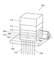
도 1은 다양한 실시예들에 따른 전자 컴포넌트(100), 예를 들어 발광 전자 컴포넌트(100)를 도시한다.1 illustrates an
다양한 실시예들에서, 전자 컴포넌트(100)는 유기 발광 다이오드(OLED)로서, 유기 포토다이오드(OPD)로서, 유기 태양 전지(OSC)로서, 또는 유기 트랜지스터로서, 예를 들어 유기 박막 트랜지스터(OTFT)로서 구현될 수 있다. 다양한 실시예들에서, 발광 전자 컴포넌트(100)는 집적 회로의 부분일 수 있다. 더욱이, 복수의 (예를 들어, 발광) 전자 컴포넌트들(100)이, 예를 들어 공통 하우징 내에 수용되는 방식으로 제공될 수 있다.In various embodiments, the
(예를 들어, 발광) 전자 컴포넌트(100)는 기판(102)을 가질 수 있다. 기판(102)은, 예를 들어 전자 엘리먼트들 또는 층들, 예를 들어 광전자 엘리먼트들을 위한 캐리어 엘리먼트로서 기능할 수 있다. 예로서, 기판(102)은 유리, 석영, 및/또는 반도체 물질 또는 임의의 다른 적합한 물질로 형성되거나 또는 포함할 수 있다. 더욱이, 기판(102)은 플라스틱 필름 또는 하나의 플라스틱 필름을 포함하는 또는 복수의 플라스틱 필름들을 포함하는 라미네이트로 형성되거나 또는 포함할 수 있다. 플라스틱은 하나 또는 둘 이상의 폴리올레핀(polyolefin)들(예를 들어, 고밀도 또는 저밀도 폴리에틸렌(PE) 또는 폴리프로필렌(PP))로 형성되거나 또는 포함할 수 있다. 더욱이, 플라스틱은 폴리비닐 염화물(PVC), 폴리스티렌(PS), 폴리에스터 및/또는 폴리카보네이트(PC), 폴리에틸렌 테레프탈레이트(PET), 폴리에테르 설폰(PES) 및/또는 폴리에틸렌 나프탈레이트(PEN)로 형성되거나 또는 포함할 수 있다. 더욱이, 기판(102)은, 예를 들어 금속 필름, 예를 들어 알루미늄 필름, 하이-그레이드 스틸 필름, 구리 필름 또는 조합 또는 그에 대한 층 스택을 포함할 수 있다. 기판(102)은 상술된 물질들 중 하나 또는 둘 이상을 포함할 수 있다. 기판(102)은 투명하게, 부분적으로 투명하게, 또는 불투명하게 구현될 수 있다.The electronic component 100 (eg, light emitting) can have a
제 1 전극(104)은 기판(102) 상에 또는 위에 적용될 수 있다. 제 1 전극(104)(이하에서 바닥측 전극(104)으로 또한 지시됨)은, 예를 들어 금속 또는 투명한 전도성 산화물(TCO), 또는 동일한 또는 상이한 금속 또는 금속들 및/또는 동일한 또는 상이한 TCO들의 복수의 층들을 포함하는 층 스택과 같은 전기적으로 전도성의 물질로 형성되거나 또는 그러한 물질일 수 있다. 투명한 전도성 산화물들은, 투명한 전도성 물질들, 예를 들어 아연 산화물, 주석 산화물, 카드뮴 산화물, 티타늄 산화물, 인듐 산화물, 또는 인듐 주석 산화물(ITO)과 같은, 예를 들어 금속 산화물들이다. 예를 들어, ZnO, SnO2, 또는 In2O3과 같은 2원 금속-산소 화합물들, 예를 들어 Zn2SnO4, CdSnO3, ZnSnO3, MgIn2O4, GaInO3, Zn2In2O5 또는 In4Sn3O12와 같은 3원 금속-산소 화합물들, 또는 상이한 투명한 전도성 산화물들의 혼합물들은 또한 함께 TCO들의 그룹에 속한다. 더욱이, TCO들은 화학량론적 조성에 반드시 대응하지는 않으며, 더욱이 p-도핑되거나 또는 n-도핑될 수 있다. 제 1 전극(104)은 애노드로서, 즉 정공-주입(hole-injecting) 물질로서 구현될 수 있다.The
다양한 실시예들에서, 제 1 전극(104)은 TCO의 층 상에 금속 층의 조합의 층 스택에 의해 형성될 수 있으며, 그 반대도 가능하다. 일 예는 인듐 주석 산화물 층(ITO) 상에 적용되는 실버 층(ITO 상의 Ag)이다. 다양한 실시예들에서, 제 1 전극(104)은 금속(예를 들어, Ag, Pt, Au, Mg)을 포함할 수 있거나 또는 기술된 물질들의 금속 합금(예를 들어, AgMg 합금)을 포함할 수 있다. 다양한 실시예들에서, 제 1 전극(104)은 AlZnO 또는 유사한 물질들을 포함할 수 있다.In various embodiments, the
다양한 실시예들에서, 제 1 전극(104)은 금속을 포함할 수 있으며, 이는, 예를 들어 캐소드 물질로서, 즉 전자-주입 물질로서 기능할 수 있다. 다양한 실시예들에서, 특히, 예를 들어 Al, Ba, In, Ag, Au, Mg, Ca 또는 Li 및 이러한 물질들의 화합물들, 조합들 또는 합금들이 캐소드 물질로서 제공될 수 있다.In various embodiments, the
발광 전자 컴포넌트(100)가 바닥측 이미터로서 설계되는 경우에 있어서, 제 1 전극(104)은, 예를 들어 대략 25㎚와 동등한 또는 그 미만의 층 두께, 예를 들어 대략 20㎚와 동등한 또는 그 미만의 층 두께, 예를 들어 대략 18㎚와 동등한 또는 그 미만의 층 두께를 가질 수 있다. 더욱이, 제 1 전극(104)은, 예를 들어 대략 10㎚와 동등한 또는 그보다 큰 층 두께, 예를 들어 대략 15㎚와 동등한 또는 그보다 큰 층 두께를 가질 수 있다. 다양한 실시예들에서, 제 1 전극(104)은 대략 10㎚ 내지 대략 25㎚의 범위의 층 두께, 예를 들어 대략 10㎚ 내지 대략 18㎚의 범위의 층 두께, 예를 들어 대략 15㎚ 내지 대략 18㎚의 범위의 층 두께를 가질 수 있다.In the case where the light emitting
발광 전자 컴포넌트(100)가 최상측 이미터로서 설계되는 경우에 있어서, 제 1 전극(104)은, 예를 들어 대략 40㎚와 동등한 또는 그보다 큰 층 두께, 예를 들어 대략 50㎚와 동등한 또는 그보다 큰 층 두께를 가질 수 있다.In the case where the light emitting
더욱이, (예를 들어, 발광) 전자 컴포넌트(100)는 제 1 전극(104) 상에 또는 위에 적용된 또는 적용되는 유기 기능층 구조(106)를 가질 수 있다.Furthermore, (eg, light emitting)
유기 기능층 구조(106)는, 예를 들어 형광성의 및/또는 인광성의 이미터들을 포함하는 하나의 또는 복수의 이미터 층들(108), 및 하나의 또는 복수의 정공-전도 층들(110)을 포함할 수 있다.The organic
이미터 층(들)(108)을 위한 다양한 실시예들에 따라, 다양한 실시예들에 따른 전자 컴포넌트에서 이용될 수 있는 이미터 물질들의 예들은, 비-폴리머성(non-polymeric) 이미터들로서, 금속 착물(metal complex)들, 예를 들어 청색 인광성 FIrPic (bis(3,5-difluoro-2-(2-pyridyl)phenyl-(2-carboxypyridyl)-iridium III), 녹색 인광성 Ir(ppy)3 (tris(2-phenylpyridine)iridium III), 적색 인광성 Ru (dtb-bpy)3*2(PF6) (tris[4,4'-di-tert-butyl-(2,2')-bipyridine]ruthenium (III) complex) 및 청색 형광성 DPAVBi (4,4-bis[4-(di-p-tolylamino)styryl]biphenyl), 녹색 형광성 TTPA (9,10-bis[N,N-di-(p-tolyl)-amino]anthracene) 및 적색 형광성 DCM2 (4-dicyanomethylene)-2-methyl-6-julolidyl-9-enyl-4H-pryane)과 같은 이리듐 착물들과, 폴리플루오렌, 폴리티오펜 및 폴리페닐렌(예를 들어, 2- 또는 2,5-치환 폴리-p-페닐렌 비닐렌(2- or 2,5-substituted poly-p-phenylene vinylene))의 유도체들과 같은 유기 또는 유기금속 화합물들을 포함한다. 이러한 비-폴리머성 이미터들은, 예를 들어 열 증발에 의해 증착될 수 있다. 더욱이, 예를 들어 특히, 스핀 코팅과 같은 습식-화학 방법들에 의해 증착될 수 있는 폴리머 이미터들을 이용하는 것이 가능하다.According to various embodiments for emitter layer (s) 108, examples of emitter materials that may be used in an electronic component in accordance with various embodiments are as non-polymeric emitters. Metal complexes, for example blue phosphorescent FIrPic (bis (3,5-difluoro-2- (2-pyridyl) phenyl- (2-carboxypyridyl) -iridium III), green phosphorescent Ir (ppy) ) 3 (tris (2-phenylpyridine) iridium III), red phosphorescent Ru (dtb-bpy) 3 * 2 (PF 6 ) (tris [4,4'-di-tert-butyl- (2,2 ')- bipyridine] ruthenium (III) complex) and blue fluorescent DPAVBi (4,4-bis [4- (di-p-tolylamino) styryl] biphenyl), green fluorescent TTPA (9,10-bis [N, N-di- ( iridium complexes such as p-tolyl) -amino] anthracene) and red fluorescent DCM2 (4-dicyanomethylene) -2-methyl-6-julolidyl-9-enyl-4H-pryane), polyfluorene, polythiophene and Derivatives of polyphenylene (e.g., 2- or 2,5-substituted poly-p-phenylene vinylene); Same organic or organometallic compounds. Such non-polymeric emitters can be deposited, for example, by thermal evaporation. Moreover, it is possible to use polymer emitters which can be deposited, for example, by wet-chemical methods, in particular, spin coating.
이미터 물질들은 적합한 방식으로 매트릭스 물질 내에 매립될 수 있다.Emitter materials may be embedded in the matrix material in a suitable manner.
전자 컴포넌트(100)의 이미터 층(들)(108)의 이미터 물질들은, 예를 들어 전자 컴포넌트(100)가 백색 광을 방출하도록 선택될 수 있다. 이미터 층(들)(108)은 상이한 색들(예를 들어, 청색 및 황색, 또는 청색, 녹색, 및 적색)로 방출하는 복수의 이미터 물질들을 포함할 수 있으며; 대안적으로, 이미터 층(들)(108)은 또한, 청색 형광성 이미터 층(108) 또는 청색 인광성 이미터 층(108), 녹색 인광성 이미터 층(108), 및 적색 인광성 이미터 층(108)과 같은 복수의 부분 층들로 구성될 수 있다. 상이한 색들을 혼합함으로써, 백색의 색 인상(color impression)을 갖는 광의 방출이 초래될 수 있다. 대안적으로, 상기 층들에 의해 발생된 1차 방출의 빔 경로 내에 컨버터 물질을 배열하기 위한 제공이 또한 이루어질 수 있으며, 상기 컨버터 물질은 1차 방사를 적어도 부분적으로 흡수하고 상이한 파장을 갖는 2차 방사를 방출하여, (아직 백색이 아닌) 1차 방사로부터, 1차 방사와 2차 방사의 조합에 의해, 백색의 색 인상이 초래된다.The emitter materials of the emitter layer (s) 108 of the
유기 기능층 구조(106)는 일반적으로 하나의 또는 복수의 기능층들을 포함할 수 있다. 하나의 또는 복수의 기능층들은 유기 폴리머들, 유기 올리고머(oligomer)들, 유기 모노머(monomer)들, 유기 작은 비-폴리머 분자들("소분자(small molecule)들") 또는 이들 물질들의 조합을 포함할 수 있다. 예로서, 유기 기능층 구조(106)는 정공 수송층(110)으로서 구현되는 하나의 또는 복수의 기능층들을 포함할 수 있어서, 예를 들어 OLED의 경우에, 전자발광 영역 또는 전자발광 층 내로의 효율적인 정공 주입을 가능하게 한다. 예로서, 3차 아민(tertiary amine)들, 카바조(carbazo) 유도체들, 전도성 폴리아닐린, 또는 폴리에틸렌 디옥시티오펜은 정공 수송층(110)을 위한 물질로서 이용될 수 있다. 다양한 실시예들에서, 하나의 또는 복수의 기능층들은 전자발광 층으로서 구현될 수 있다.The organic
다양한 실시예들에서, 정공 수송층(110)은 제 1 전극(104) 상에 또는 위에 적용, 예를 들어 증착될 수 있으며, 이미터 층(108)은 정공 수송층(110) 상에 또는 위에 적용, 예를 들어 증착될 수 있다.In various embodiments, the
전자 컴포넌트(100)는 일반적으로, 전자 컴포넌트(100)의 기능성을, 따라서 효율성을 더 개선하도록 기능하는 추가의 유기 기능층들을 포함할 수 있다.
발광 전자 컴포넌트(100)는 "바닥측 이미터" 및/또는 "최상측 이미터"로서 구현될 수 있다.The light emitting
다양한 실시예들에서, 유기 기능층 구조(106)는, 최대 대략 1.5㎛의 층 두께, 예를 들어 최대 대략 1.2㎛의 층 두께, 예를 들어 최대 대략 1㎛의 층 두께, 예를 들어 최대 대략 800㎚의 층 두께, 예를 들어 최대 대략 500㎚의 층 두께, 예를 들어 최대 대략 400㎚의 층 두께, 예를 들어 최대 대략 300㎚의 층 두께를 가질 수 있다. 다양한 실시예들에서, 유기 기능층 구조(106)는, 예를 들어 직접적으로(directly) 층층이 배열된 복수의 OLED들의 스택을 가질 수 있고, 각각의 OLED는, 예를 들어 최대 대략 1.5㎛의 층 두께, 예를 들어 최대 대략 1.2㎛의 층 두께, 예를 들어 최대 대략 1㎛의 층 두께, 예를 들어 최대 대략 800㎚의 층 두께, 예를 들어 최대 대략 500㎚의 층 두께, 예를 들어 최대 대략 400㎚의 층 두께, 예를 들어 최대 대략 300㎚의 층 두께를 가질 수 있다. 다양한 실시예들에서, 유기 기능층 구조(106)는, 예를 들어 직접적으로 층층이 배열된 3개 또는 4개의 OLED들의 스택을 가질 수 있으며, 이러한 경우에 예를 들어, 유기 기능층 구조(106)는 최대 대략 3㎛의 층 두께를 가질 수 있다.In various embodiments, the organic
제 2 전극(112)은 유기 기능층 구조(106) 상에 또는 위에 적용될 수 있다.The
제 2 전극(112)은, 제 2 전극(112) 상에 또는 위에 적용된 유전체층(114)이 유기 기능층 구조(106)에 광학적으로 결합되는 방식으로 설계될 수 있다. 제 2 전극(112)은 유기 기능층 구조(106)에 의해 방출되는 방사에 관하여 반투명할 수 있다. 다양한 실시예들에서, 제 2 전극(112)은, 유기 기능층 구조(106)와 유전체층(114) 사이의 충분한 결합 강도(제 2 전극(112)의 층 두께가 더 클수록, 결합 강도는 더 낮아짐), 발광 컴포넌트(100)의 달성가능한 효율성, 그리고 따라서 연색 평가 지수(제 2 전극(112)의 층 두께가 더 클수록, 효율성은 더 커짐) 사이에서, 원하는 절충안(compromise)이 선택되는 방식으로 층 두께를 가질 수 있다. 다양한 실시예들에서, 제 2 전극(112)은 제 1 전극(104)과 동일한 물질들로 형성되거나 포함할 수 있으며, 다양한 실시예들에서 금속들이 특히 적합하다.The
다양한 실시예들에서, 제 2 전극(112)은, 예를 들어 대략 50㎚와 동등한 또는 그 미만의 층 두께, 예를 들어 대략 45㎚와 동등한 또는 그 미만의 층 두께, 예를 들어 대략 40㎚와 동등한 또는 그 미만의 층 두께, 예를 들어 대략 35㎚와 동등한 또는 그 미만의 층 두께, 예를 들어 대략 30㎚와 동등한 또는 그 미만의 층 두께, 예를 들어 대략 25㎚와 동등한 또는 그 미만의 층 두께, 예를 들어 대략 20㎚와 동등한 또는 그 미만의 층 두께, 예를 들어 대략 15㎚와 동등한 또는 그 미만의 층 두께, 예를 들어 대략 10㎚와 동등한 또는 그 미만의 층 두께를 가질 수 있다.In various embodiments, the
유전체층(114)(또한 이하에서 (투명한) 중간층으로서 지시됨)은 제 2 전극(112) 상에 또는 위에 있을 수 있거나 또는 적용될 수 있다.The dielectric layer 114 (also referred to hereinafter as a (transparent) intermediate layer) may be on or over the
유전체층(114)은, 380㎚ 내지 780㎚의 파장 범위의 적어도 부분 범위의 방사에 투명한 층일 수 있다. 예를 들어, 발광 단색성(monochrome) 또는 방출-스펙트럼-제한된 전자 컴포넌트가 제공되도록 의도되는 경우에 있어서, 유전체층(114)은, 원하는 단색성 광의 파장 범위의 적어도 부분 범위의 방사에 또는 제한된 방출 스펙트럼에 대해 투명하기에 충분하다.The
다양한 실시예들에서, 유전체층(114)은 ALD 방법에 의해 증착되고, 이에 의해 유전체층(114)은 원자층 증착 층으로서 형성된다. 다양한 실시예들에서, 유전체층(114)은, 대략 50㎚ 내지 대략 2㎛의 범위의, 예를 들어 대략 70㎚ 내지 대략 200㎚의 범위의, 예를 들어 대략 100㎚ 내지 대략 120㎚의 범위의 층 두께로 증착된다. 이러한 층 두께들의 경우에, 캡슐화 효과가 보장되고 결합된 미세공동의 두께는 예를 들어, 매우 정확하게 설정될 수 있다. 유전체층(114)은, 예를 들어 SiO2; Si3N4; SiON(이들 물질들은, 예를 들어 CVD 방법에 의해 증착됨); Al2O3; ZrO2; TiO2; Ta2O5; SiO2; ZnO; 및/또는 HfO2(이들 물질들은, 예를 들어 ALD 방법에 의해 증착됨); 또는 이러한 물질들의 조합과 같은 물질 또는 물질들의 혼합물 또는 물질들의 층들의 스택을 포함할 수 있다.In various embodiments,
반사층 구조(116)는 유전체층(114) 상에 또는 위에 있을 수 있거나 또는 적용될 수 있다.
반사층 구조(116)는 제 1 전극(102)과 동일한 물질들로 형성될 수 있으며, 발광 전자 컴포넌트(100)가 최상측 이미터로서 설계되는 경우에, 반사층 구조(116)가, 예를 들어 대략 25㎚와 동등한 또는 그 미만의 층 두께, 예를 들어 대략 20㎚와 동등한 또는 그 미만의 층 두께, 예를 들어 대략 18㎚와 동등한 또는 그 미만의 층 두께를 가질 수 있는 방식으로 층 두께가 선택될 수 있다. 더욱이, 제 1 전극(104)은, 예를 들어 대략 10㎚와 동등한 또는 그보다 큰 층 두께, 예를 들어 대략 15㎚와 동등한 또는 그보다 큰 층 두께를 가질 수 있다. 다양한 실시예들에서, 반사층 구조(116)는 대략 10㎚ 내지 대략 25㎚의 범위의 층 두께, 예를 들어 대략 10㎚ 내지 대략 18㎚의 범위의 층 두께, 예를 들어 대략 15㎚ 내지 대략 18㎚의 범위의 층 두께를 가질 수 있다.The
발광 전자 컴포넌트(100)가 바닥측 이미터로서 설계되는 경우에 있어서, 반사층 구조(116)는 예를 들어 대략 40㎚와 동등한 또는 그보다 큰 층 두께, 예를 들어 대략 50㎚와 동등한 또는 그보다 큰 층 두께를 가질 수 있다.In the case where the light emitting
반사층 구조(116)는 하나의 또는 복수의 미러들을 가질 수 있다. 반사층 구조(116)가 복수의 미러들을 갖는 경우, 각각의 미러들은 각각의 유전체층에 의해 서로 분리된다.
도 1에 예시된 발광 전자 컴포넌트(100)는, 광 빔들(118)에 의해 상징되는 바와 같이 바닥측 이미터로서 설계된다.The light emitting
발광 전자 컴포넌트(100)를 제조할 때 ALD 방법 및 CVD 방법의 도움으로, 유전체층(114)은, 매우 정확하게 설정될 수 있는 층 두께로, ALD 방법에 의해 증착될 수 있다. 다양한 실시예들에서, 서로 광학적으로 결합된 2개의 미세공동들을 갖는 종래의 유기 발광 다이오드에 제공되는 제 2 유기층은, 하나의 조밀한 유전체층에 의해 확실하게 대체된다.With the aid of the ALD method and the CVD method in manufacturing the light emitting
다양한 실시예들에서, 적용된 유전체층(114)은 캡슐화 효과를 가져서, 형성되는 전자 컴포넌트, 그리고 이러한 경우에 예를 들어, 유기 기능층 구조(106)는 공기 또는 물의 침투로부터 보호된다.In various embodiments, the applied
기술적 지시들에 의해 지배되는 방식에서, ALD 방법은, 유기 물질들의 기상 증착보다 상당히 더 적은 층 두께 변동을 가지며, 그 결과, 다양한 실시예들에 따라, 예를 들어 결합된-미세공동 OLED들의 산업적 규모의 이용이 가능해진다. 예로서, 이는, 예를 들어 유전체층(114)의 층 두께의 설정에 의해 유기층들의 층 두께 변동들을 또한 보상할 가능성을 제공하며, 이는 산업적 규모의 설비들에서의 수율을 증가시킬 수 있다.In a manner governed by technical instructions, the ALD method has significantly less layer thickness variation than vapor deposition of organic materials, and as a result, according to various embodiments, for example, industrial of combined-microcavity OLEDs. The scale can be used. By way of example, this offers the possibility to also compensate for the layer thickness variations of the organic layers, for example by setting the layer thickness of the
다양한 실시예들에서, 다양한 실시예들에 따른 복수의 또는 다수의 발광 전자 컴포넌트들(100)을 갖는 조명 디바이스 또는 디스플레이 디바이스가 제공될 수 있다. 조명 디바이스 또는 디스플레이 디바이스는 대면적 방식(large-area fashion)으로 구현되는 활성 루미너스 영역을 가질 수 있다. 다양한 실시예들에서, "대면적 방식으로"는, 루미너스 영역이 수 제곱 밀리미터와 동등한 또는 그보다 큰, 예를 들어 수 제곱 센티미터와 동등한 또는 그보다 큰, 예를 들어 수 제곱 데시미터와 동등한 또는 그보다 큰 면적을 갖는다는 것을 의미할 수 있다.In various embodiments, an illumination device or display device may be provided having a plurality or a plurality of light emitting
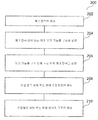
도 2는 일 실시예에 따른 발광 전자 컴포넌트를 제조하기 위한 방법을 예시하는 흐름도(200)를 도시한다.2 shows a
202에서 제 1 전극이 형성되고, 204에서 제 1 전극 상에 또는 위에 유기 기능층 구조가 형성된다. 더욱이, 206에서 유기 기능층 구조 상에 또는 위에 제 2 전극이 형성되고, 208에서 제 2 전극 상에 또는 위에 유전체층이 형성된다. 마지막으로, 210에서 유전체층 상에 또는 위에 반사층 구조가 형성된다.A first electrode is formed at 202 and an organic functional layer structure is formed on or over the first electrode at 204. Moreover, a second electrode is formed on or over the organic functional layer structure at 206, and a dielectric layer is formed on or over the second electrode at 208. Finally, at 210 a reflective layer structure is formed on or over the dielectric layer.
Claims (16)
제 1 전극(104);
상기 제 1 전극(104) 상의 또는 위의 유기 기능층 구조(106);
상기 유기 기능층 구조(106) 상의 또는 위의 제 2 전극(112);
상기 제 2 전극(112) 상의 또는 위의 유전체층(114); 및
상기 유전체층(114) 상의 또는 위의 반사층 구조(116)
를 포함하며,
상기 유기 기능층 구조(106)는 상기 제 1 전극(104)과 상기 제 2 전극(112) 사이에 제 1 미세공동(microcavity)을 형성하고, 상기 유전체층(114)은 상기 제 2 전극(112)과 상기 반사층 구조(116) 사이에 제 2 미세공동을 형성하는,
전자 컴포넌트.As electronic component 100,
First electrode 104;
An organic functional layer structure (106) on or above the first electrode (104);
A second electrode 112 on or above the organic functional layer structure 106;
A dielectric layer 114 on or above the second electrode 112; And
Reflective layer structure 116 on or above the dielectric layer 114.
Including;
The organic functional layer structure 106 forms a first microcavity between the first electrode 104 and the second electrode 112, and the dielectric layer 114 forms the second electrode 112. And forming a second microcavity between the reflective layer structure 116,
Electronic component.
상기 제 2 전극(112)은, 상기 제 1 미세공동이 상기 제 2 전극(112)을 통해 상기 제 2 미세공동에 광학적으로 결합되는 방식으로 설계되는,
전자 컴포넌트.The method of claim 1,
The second electrode 112 is designed in such a way that the first microcavity is optically coupled to the second microcavity through the second electrode 112.
Electronic component.
상기 제 2 전극(112)은 상기 유기 기능층 구조(106)에 의해 방출되는 방사에 관하여 반투명한,
전자 컴포넌트.3. The method of claim 2,
The second electrode 112 is translucent with respect to radiation emitted by the organic functional layer structure 106,
Electronic component.
상기 유전체층(114)은, 380㎚ 내지 780㎚의 파장 범위의 적어도 부분 범위의 방사에 투명한 층인,
전자 컴포넌트.The method according to any one of claims 1 to 3,
The dielectric layer 114 is a layer that is transparent to radiation in at least a partial range of the wavelength range of 380 nm to 780 nm,
Electronic component.
상기 유전체층(114)은,
화학 기상 증착 방법;
물리 기상 증착 방법;
스핀 코팅 방법;
프린팅;
블레이드 코팅;
스프레잉; 및
딥 코팅 방법 중 하나의 방법에 의해 적용된 층인,
전자 컴포넌트.The method according to any one of claims 1 to 4,
The dielectric layer 114,
Chemical vapor deposition methods;
Physical vapor deposition method;
Spin coating method;
Printing;
Blade coating;
Spraying; And
A layer applied by one of the dip coating methods,
Electronic component.
상기 유전체층(114)은 원자층 증착 층인,
전자 컴포넌트.6. The method according to any one of claims 1 to 5,
The dielectric layer 114 is an atomic layer deposition layer,
Electronic component.
상기 유전체층(114)은 대략 50㎚ 내지 대략 2㎛의 범위의, 바람직하게 대략 70㎚ 내지 대략 200㎚의 범위의 층 두께를 갖는,
전자 컴포넌트.7. The method according to any one of claims 1 to 6,
The dielectric layer 114 has a layer thickness in the range of about 50 nm to about 2 μm, preferably in the range of about 70 nm to about 200 nm,
Electronic component.
상기 유전체층(114)은, SiO2; Si3N4; SiON; Al2O3; ZrO2; TiO2; Ta2O5; SiO2; ZnO; 및 HfO2; 또는 상기 물질들의 조합으로 이루어진 그룹으로부터 선택된 물질 또는 물질들의 혼합물 또는 물질들의 층들의 스택을 포함하는,
전자 컴포넌트.The method according to any one of claims 1 to 7,
The dielectric layer 114 may be SiO 2 ; Si 3 N 4 ; SiON; Al 2 O 3 ; ZrO 2; TiO 2 ; Ta 2 O 5 ; SiO 2 ; ZnO; And HfO 2 ; Or a stack of layers of materials or a mixture of materials or a material selected from the group consisting of combinations of the above materials,
Electronic component.
제 1 전극(104)을 형성하는 단계(202);
상기 제 1 전극(104) 상에 또는 위에 유기 기능층 구조(106)를 형성하는 단계(204);
상기 유기 기능층 구조(106) 상에 또는 위에 제 2 전극(112)을 형성하는 단계(206);
상기 제 2 전극(112) 상에 또는 위에 유전체층(114)을 형성하는 단계(208); 및
상기 유전체층(114) 상에 또는 위에 반사층 구조(116)를 형성하는 단계(210)
를 포함하여서,
상기 유기 기능층 구조(106)는 상기 제 1 전극(104)과 상기 제 2 전극(112) 사이에 제 1 미세공동을 형성하고,
상기 유전체층(114)은 상기 제 2 전극(112)과 상기 반사층 구조(116) 사이에 제 2 미세공동을 형성하는,
전자 컴포넌트를 제조하기 위한 방법.As a method 200 for manufacturing an electronic component 100,
Forming (202) a first electrode (104);
Forming (204) an organic functional layer structure (106) on or over the first electrode (104);
Forming (206) a second electrode (112) on or above the organic functional layer structure (106);
Forming (208) a dielectric layer (114) on or over the second electrode (112); And
Forming 210 a reflective layer structure 116 on or over the dielectric layer 114
Including,
The organic functional layer structure 106 forms a first microcavity between the first electrode 104 and the second electrode 112,
The dielectric layer 114 forms a second microcavity between the second electrode 112 and the reflective layer structure 116,
Method for manufacturing an electronic component.
상기 제 2 전극(112)은, 상기 제 1 미세공동이 상기 제 2 미세공동에 광학적으로 결합되는 방식으로 형성되는,
전자 컴포넌트를 제조하기 위한 방법.The method of claim 9,
The second electrode 112 is formed in such a manner that the first microcavity is optically coupled to the second microcavity.
Method for manufacturing an electronic component.
상기 제 2 전극(112)은 상기 유기 기능층 구조(106)에 의해 방출되는 방사에 관하여 반투명하게 형성되는,
전자 컴포넌트를 제조하기 위한 방법.11. The method of claim 10,
The second electrode 112 is formed translucent with respect to radiation emitted by the organic functional layer structure 106,
Method for manufacturing an electronic component.
상기 유전체층(114)은, 380㎚ 내지 780㎚의 파장 범위의 적어도 부분 범위의 방사에 투명한 층으로서 형성되는,
전자 컴포넌트를 제조하기 위한 방법.12. The method according to any one of claims 9 to 11,
The dielectric layer 114 is formed as a layer transparent to radiation in at least a partial range of the wavelength range of 380 nm to 780 nm,
Method for manufacturing an electronic component.
상기 유전체층(114)은,
화학 기상 증착 방법;
물리 기상 증착 방법;
스핀 코팅 방법;
프린팅;
블레이드 코팅;
스프레잉; 및
딥 코팅 방법 중 하나의 방법에 의해 형성되는,
전자 컴포넌트를 제조하기 위한 방법.13. The method according to any one of claims 9 to 12,
The dielectric layer 114,
Chemical vapor deposition methods;
Physical vapor deposition method;
Spin coating method;
Printing;
Blade coating;
Spraying; And
Formed by one of the dip coating methods,
Method for manufacturing an electronic component.
상기 유전체층(114)은 원자층 증착 방법에 의해 적용되는,
전자 컴포넌트를 제조하기 위한 방법.14. The method according to any one of claims 9 to 13,
The dielectric layer 114 is applied by an atomic layer deposition method,
Method for manufacturing an electronic component.
상기 유전체층(114)은 대략 50㎚ 내지 대략 2㎛의 범위의, 바람직하게 대략 70㎚ 내지 대략 200㎚의 범위의 층 두께로 형성되는,
전자 컴포넌트를 제조하기 위한 방법.15. The method according to any one of claims 9 to 14,
The dielectric layer 114 is formed with a layer thickness in the range of about 50 nm to about 2 μm, preferably in the range of about 70 nm to about 200 nm,
Method for manufacturing an electronic component.
상기 유전체층(114)은, SiO2; Si3N4; SiON; Al2O3; ZrO2; TiO2; Ta2O5; SiO2; ZnO; 및 HfO2; 또는 상기 물질들의 조합으로 이루어진 그룹으로부터 선택된 물질 또는 물질들의 혼합물 또는 물질들의 층들의 스택으로 형성되는,
전자 컴포넌트를 제조하기 위한 방법.16. The method according to any one of claims 9 to 15,
The dielectric layer 114 may be SiO 2 ; Si 3 N 4 ; SiON; Al 2 O 3 ; ZrO 2; TiO 2 ; Ta 2 O 5 ; SiO 2 ; ZnO; And HfO 2 ; Or a stack of layers of materials or a mixture of materials or a material selected from the group consisting of combinations of the above materials,
Method for manufacturing an electronic component.
Applications Claiming Priority (3)
| Application Number | Priority Date | Filing Date | Title |
|---|---|---|---|
| DE102010042982A DE102010042982A1 (en) | 2010-10-27 | 2010-10-27 | Electronic component and method for manufacturing an electronic component |
| DE102010042982.1 | 2010-10-27 | ||
| PCT/EP2011/067643 WO2012055694A1 (en) | 2010-10-27 | 2011-10-10 | Electronic component and method for producing an electronic component |
Publications (1)
| Publication Number | Publication Date |
|---|---|
| KR20130086052A true KR20130086052A (en) | 2013-07-30 |
Family
ID=45531621
Family Applications (1)
| Application Number | Title | Priority Date | Filing Date |
|---|---|---|---|
| KR1020137013568A KR20130086052A (en) | 2010-10-27 | 2011-10-10 | Electronic component and method for producing an electronic component |
Country Status (7)
| Country | Link |
|---|---|
| US (1) | US20130270536A1 (en) |
| EP (1) | EP2633568A1 (en) |
| JP (1) | JP2013545230A (en) |
| KR (1) | KR20130086052A (en) |
| CN (1) | CN103210518A (en) |
| DE (1) | DE102010042982A1 (en) |
| WO (1) | WO2012055694A1 (en) |
Families Citing this family (6)
| Publication number | Priority date | Publication date | Assignee | Title |
|---|---|---|---|---|
| CN103545449A (en) * | 2012-07-10 | 2014-01-29 | 群康科技(深圳)有限公司 | Organic light emitting diode (OLED), display panel with OLED and display equipment with OLED |
| CN109427988B (en) * | 2017-08-21 | 2021-02-12 | 上海和辉光电股份有限公司 | Display panel and display device |
| CN108365115B (en) * | 2017-08-29 | 2019-07-19 | 广东聚华印刷显示技术有限公司 | Electroluminescent device, display panel and preparation method thereof |
| JP6816780B2 (en) * | 2019-01-09 | 2021-01-20 | セイコーエプソン株式会社 | Organic electroluminescence equipment, manufacturing method of organic electroluminescence equipment, head-mounted display and electronic equipment |
| CN111628102A (en) * | 2020-05-18 | 2020-09-04 | 武汉华星光电半导体显示技术有限公司 | Microcavity electrode structure and organic electroluminescent device |
| CN116487401A (en) * | 2022-01-17 | 2023-07-25 | 华为技术有限公司 | Display panel and electronic device |
Family Cites Families (14)
| Publication number | Priority date | Publication date | Assignee | Title |
|---|---|---|---|---|
| CA2277654A1 (en) * | 1999-07-19 | 2001-01-19 | Luxell Technologies Inc. | Electroluminescent display packaging and method therefor |
| WO2003105248A1 (en) * | 2002-06-11 | 2003-12-18 | Luxell Technologies Inc. | Oled display with contrast enhancing interference members |
| EP1403939B1 (en) * | 2002-09-30 | 2006-03-01 | Kabushiki Kaisha Toyota Jidoshokki | Light-emitting device, display and lighting unit |
| JP4155569B2 (en) * | 2003-08-27 | 2008-09-24 | 株式会社日立製作所 | High efficiency organic light emitting device |
| US20050093437A1 (en) * | 2003-10-31 | 2005-05-05 | Ouyang Michael X. | OLED structures with strain relief, antireflection and barrier layers |
| TWI231723B (en) * | 2004-04-16 | 2005-04-21 | Ind Tech Res Inst | Organic electroluminescence display device |
| JP4363365B2 (en) * | 2004-07-20 | 2009-11-11 | 株式会社デンソー | Color organic EL display and manufacturing method thereof |
| US20060109397A1 (en) * | 2004-11-24 | 2006-05-25 | Organic Lighting Technologies Llc | Organic light emitting diode backlight inside LCD |
| KR100715500B1 (en) * | 2004-11-30 | 2007-05-07 | (주)케이디티 | Light source with micro-cavity organic light emitting diode and photoluminescent layer |
| US20060197436A1 (en) * | 2005-03-01 | 2006-09-07 | Sharp Laboratories Of America, Inc. | ZnO nanotip electrode electroluminescence device on silicon substrate |
| JP2008047340A (en) * | 2006-08-11 | 2008-02-28 | Dainippon Printing Co Ltd | Organic electroluminescence device |
| US7728512B2 (en) * | 2007-03-02 | 2010-06-01 | Universal Display Corporation | Organic light emitting device having an external microcavity |
| JP5141894B2 (en) * | 2008-04-17 | 2013-02-13 | 住友金属鉱山株式会社 | Dielectric multilayer mirror and manufacturing method thereof |
| FR2933538B1 (en) * | 2008-07-07 | 2012-09-21 | Commissariat Energie Atomique | DISPLAY, LIGHTING OR SIGNALING ELECTROLUMINESCENT DEVICE AND METHOD FOR MANUFACTURING THE SAME |
-
2010
- 2010-10-27 DE DE102010042982A patent/DE102010042982A1/en not_active Withdrawn
-
2011
- 2011-10-10 KR KR1020137013568A patent/KR20130086052A/en not_active Application Discontinuation
- 2011-10-10 US US13/881,761 patent/US20130270536A1/en not_active Abandoned
- 2011-10-10 EP EP11772918.6A patent/EP2633568A1/en not_active Ceased
- 2011-10-10 JP JP2013535348A patent/JP2013545230A/en active Pending
- 2011-10-10 WO PCT/EP2011/067643 patent/WO2012055694A1/en active Application Filing
- 2011-10-10 CN CN2011800518797A patent/CN103210518A/en active Pending
Also Published As
| Publication number | Publication date |
|---|---|
| JP2013545230A (en) | 2013-12-19 |
| WO2012055694A1 (en) | 2012-05-03 |
| US20130270536A1 (en) | 2013-10-17 |
| EP2633568A1 (en) | 2013-09-04 |
| CN103210518A (en) | 2013-07-17 |
| DE102010042982A1 (en) | 2012-05-03 |
Similar Documents
| Publication | Publication Date | Title |
|---|---|---|
| US8963143B2 (en) | Organic electroluminescent device | |
| US9130196B2 (en) | Light-emitting component and method for producing a light-emitting component | |
| US9887379B2 (en) | Electrode and optoelectronic component and method for producing an optoelectronic component | |
| US20150027541A1 (en) | Electronic component with moisture barrier layer | |
| US9172057B2 (en) | Encapsulation structure for an opto-electronic component | |
| KR101650029B1 (en) | Light-emitting components and method for producing a light-emitting component | |
| US10361396B2 (en) | Optoelectronic component with multilayer encapsulant CTE matched to electrode | |
| US20140225086A1 (en) | Organic light-emitting component and method for producing an organic light-emitting component | |
| US9419244B2 (en) | Organic light-emitting element and method of producing an organic light-emitting element | |
| US20160329515A1 (en) | Organic light-emitting component and method for producing an organic light-emitting component | |
| US20130270536A1 (en) | Electronic component and method for producing an electronic component | |
| KR101572114B1 (en) | Method for producing an optoelectronic component, and optoelectronic component | |
| KR20110092582A (en) | Organic light emitting diode device and method for manufacturing the same | |
| WO2016188042A1 (en) | Electroluminescent component, manufacturing method therefor, display substrate, and display device | |
| US20140319482A1 (en) | Light-emitting component and method for producing a light-emitting component | |
| US9431635B2 (en) | Light-emitting component and method for producing a light-emitting component | |
| US9818982B2 (en) | Optoelectronic assembly and method for producing an optoelectronic assembly | |
| KR102304282B1 (en) | Optoelectronic component and a method for producing an optoelectronic component | |
| US20160372699A1 (en) | Optoelectronic component and method for the production thereof | |
| US20130270542A1 (en) | Method for producing an optoelectronic component and optoelectronic component | |
| US9257492B2 (en) | Method for producing a passive electronic component, method for producing an optoelectronic assembly and passive electronic component | |
| KR20120025148A (en) | Passive matrix organic light emitting diode having anti-oxidant and anti-scattering layer and its manufacturing method |
Legal Events
| Date | Code | Title | Description |
|---|---|---|---|
| A201 | Request for examination | ||
| E902 | Notification of reason for refusal | ||
| E601 | Decision to refuse application | ||
| J201 | Request for trial against refusal decision | ||
| N231 | Notification of change of applicant | ||
| J301 | Trial decision |
Free format text: TRIAL DECISION FOR APPEAL AGAINST DECISION TO DECLINE REFUSAL REQUESTED 20150421 Effective date: 20151130 Free format text: TRIAL NUMBER: 2015101002197; TRIAL DECISION FOR APPEAL AGAINST DECISION TO DECLINE REFUSAL REQUESTED 20150421 Effective date: 20151130 |