JP2013545230A - Electronic device and method for manufacturing electronic device - Google Patents
Electronic device and method for manufacturing electronic device Download PDFInfo
- Publication number
- JP2013545230A JP2013545230A JP2013535348A JP2013535348A JP2013545230A JP 2013545230 A JP2013545230 A JP 2013545230A JP 2013535348 A JP2013535348 A JP 2013535348A JP 2013535348 A JP2013535348 A JP 2013535348A JP 2013545230 A JP2013545230 A JP 2013545230A
- Authority
- JP
- Japan
- Prior art keywords
- electrode
- electronic device
- layer
- dielectric layer
- organic functional
- Prior art date
- Legal status (The legal status is an assumption and is not a legal conclusion. Google has not performed a legal analysis and makes no representation as to the accuracy of the status listed.)
- Pending
Links
- 238000000034 method Methods 0.000 title claims description 57
- 238000004519 manufacturing process Methods 0.000 title claims description 7
- 239000010410 layer Substances 0.000 claims abstract description 186
- 239000002346 layers by function Substances 0.000 claims abstract description 42
- 239000000463 material Substances 0.000 claims description 48
- 238000005229 chemical vapour deposition Methods 0.000 claims description 13
- -1 Si 3 N 4 Inorganic materials 0.000 claims description 12
- 238000003877 atomic layer epitaxy Methods 0.000 claims description 10
- 238000005240 physical vapour deposition Methods 0.000 claims description 10
- 229910004298 SiO 2 Inorganic materials 0.000 claims description 8
- 239000000203 mixture Substances 0.000 claims description 7
- 229910018072 Al 2 O 3 Inorganic materials 0.000 claims description 6
- 229910010413 TiO 2 Inorganic materials 0.000 claims description 5
- 238000000151 deposition Methods 0.000 claims description 5
- 238000004528 spin coating Methods 0.000 claims description 5
- 238000003618 dip coating Methods 0.000 claims description 4
- 239000007921 spray Substances 0.000 claims description 4
- 229910052814 silicon oxide Inorganic materials 0.000 claims description 3
- GEIAQOFPUVMAGM-UHFFFAOYSA-N ZrO Inorganic materials [Zr]=O GEIAQOFPUVMAGM-UHFFFAOYSA-N 0.000 claims 2
- 239000007858 starting material Substances 0.000 description 22
- 238000000231 atomic layer deposition Methods 0.000 description 18
- 229910052751 metal Inorganic materials 0.000 description 12
- 239000002184 metal Substances 0.000 description 12
- XLOMVQKBTHCTTD-UHFFFAOYSA-N Zinc monoxide Chemical compound [Zn]=O XLOMVQKBTHCTTD-UHFFFAOYSA-N 0.000 description 10
- 230000015572 biosynthetic process Effects 0.000 description 8
- 239000000758 substrate Substances 0.000 description 8
- 239000012044 organic layer Substances 0.000 description 7
- 238000006243 chemical reaction Methods 0.000 description 6
- 239000011787 zinc oxide Substances 0.000 description 5
- 238000011161 development Methods 0.000 description 4
- 230000018109 developmental process Effects 0.000 description 4
- 238000005538 encapsulation Methods 0.000 description 4
- 230000005525 hole transport Effects 0.000 description 4
- XLYOFNOQVPJJNP-UHFFFAOYSA-N water Substances O XLYOFNOQVPJJNP-UHFFFAOYSA-N 0.000 description 4
- QVGXLLKOCUKJST-UHFFFAOYSA-N atomic oxygen Chemical compound [O] QVGXLLKOCUKJST-UHFFFAOYSA-N 0.000 description 3
- 238000000295 emission spectrum Methods 0.000 description 3
- 230000005693 optoelectronics Effects 0.000 description 3
- 229910052760 oxygen Inorganic materials 0.000 description 3
- 239000001301 oxygen Substances 0.000 description 3
- 238000000623 plasma-assisted chemical vapour deposition Methods 0.000 description 3
- 229920000642 polymer Polymers 0.000 description 3
- 239000004065 semiconductor Substances 0.000 description 3
- 229910052709 silver Inorganic materials 0.000 description 3
- 239000002356 single layer Substances 0.000 description 3
- FWXNJWAXBVMBGL-UHFFFAOYSA-N 9-n,9-n,10-n,10-n-tetrakis(4-methylphenyl)anthracene-9,10-diamine Chemical compound C1=CC(C)=CC=C1N(C=1C2=CC=CC=C2C(N(C=2C=CC(C)=CC=2)C=2C=CC(C)=CC=2)=C2C=CC=CC2=1)C1=CC=C(C)C=C1 FWXNJWAXBVMBGL-UHFFFAOYSA-N 0.000 description 2
- 108010043121 Green Fluorescent Proteins Proteins 0.000 description 2
- 239000004743 Polypropylene Substances 0.000 description 2
- 229910045601 alloy Inorganic materials 0.000 description 2
- 239000000956 alloy Substances 0.000 description 2
- 229910052782 aluminium Inorganic materials 0.000 description 2
- 239000010406 cathode material Substances 0.000 description 2
- 239000003086 colorant Substances 0.000 description 2
- 150000001875 compounds Chemical class 0.000 description 2
- 239000004020 conductor Substances 0.000 description 2
- 230000008021 deposition Effects 0.000 description 2
- ZUOUZKKEUPVFJK-UHFFFAOYSA-N diphenyl Chemical compound C1=CC=CC=C1C1=CC=CC=C1 ZUOUZKKEUPVFJK-UHFFFAOYSA-N 0.000 description 2
- 239000011521 glass Substances 0.000 description 2
- AMGQUBHHOARCQH-UHFFFAOYSA-N indium;oxotin Chemical compound [In].[Sn]=O AMGQUBHHOARCQH-UHFFFAOYSA-N 0.000 description 2
- 238000002347 injection Methods 0.000 description 2
- 239000007924 injection Substances 0.000 description 2
- UEEXRMUCXBPYOV-UHFFFAOYSA-N iridium;2-phenylpyridine Chemical compound [Ir].C1=CC=CC=C1C1=CC=CC=N1.C1=CC=CC=C1C1=CC=CC=N1.C1=CC=CC=C1C1=CC=CC=N1 UEEXRMUCXBPYOV-UHFFFAOYSA-N 0.000 description 2
- 150000002739 metals Chemical class 0.000 description 2
- 150000002902 organometallic compounds Chemical class 0.000 description 2
- 150000002927 oxygen compounds Chemical class 0.000 description 2
- 229920003023 plastic Polymers 0.000 description 2
- 239000004033 plastic Substances 0.000 description 2
- 239000002985 plastic film Substances 0.000 description 2
- 229920000139 polyethylene terephthalate Polymers 0.000 description 2
- 239000005020 polyethylene terephthalate Substances 0.000 description 2
- 229920001155 polypropylene Polymers 0.000 description 2
- 238000007740 vapor deposition Methods 0.000 description 2
- 239000011701 zinc Substances 0.000 description 2
- ZNJRONVKWRHYBF-VOTSOKGWSA-N 4-(dicyanomethylene)-2-methyl-6-julolidyl-9-enyl-4h-pyran Chemical compound O1C(C)=CC(=C(C#N)C#N)C=C1\C=C\C1=CC(CCCN2CCC3)=C2C3=C1 ZNJRONVKWRHYBF-VOTSOKGWSA-N 0.000 description 1
- OSQXTXTYKAEHQV-WXUKJITCSA-N 4-methyl-n-[4-[(e)-2-[4-[4-[(e)-2-[4-(4-methyl-n-(4-methylphenyl)anilino)phenyl]ethenyl]phenyl]phenyl]ethenyl]phenyl]-n-(4-methylphenyl)aniline Chemical compound C1=CC(C)=CC=C1N(C=1C=CC(\C=C\C=2C=CC(=CC=2)C=2C=CC(\C=C\C=3C=CC(=CC=3)N(C=3C=CC(C)=CC=3)C=3C=CC(C)=CC=3)=CC=2)=CC=1)C1=CC=C(C)C=C1 OSQXTXTYKAEHQV-WXUKJITCSA-N 0.000 description 1
- TXNLQUKVUJITMX-UHFFFAOYSA-N 4-tert-butyl-2-(4-tert-butylpyridin-2-yl)pyridine Chemical compound CC(C)(C)C1=CC=NC(C=2N=CC=C(C=2)C(C)(C)C)=C1 TXNLQUKVUJITMX-UHFFFAOYSA-N 0.000 description 1
- RYGMFSIKBFXOCR-UHFFFAOYSA-N Copper Chemical compound [Cu] RYGMFSIKBFXOCR-UHFFFAOYSA-N 0.000 description 1
- 229910017911 MgIn Inorganic materials 0.000 description 1
- MVMBITSRQNHOLP-UHFFFAOYSA-N OC(=O)C1=NC=CC=C1[Ir]C1=CC(F)=CC(F)=C1C1=CC=CC=N1 Chemical compound OC(=O)C1=NC=CC=C1[Ir]C1=CC(F)=CC(F)=C1C1=CC=CC=N1 MVMBITSRQNHOLP-UHFFFAOYSA-N 0.000 description 1
- 229920001609 Poly(3,4-ethylenedioxythiophene) Polymers 0.000 description 1
- 229920012266 Poly(ether sulfone) PES Polymers 0.000 description 1
- 239000004698 Polyethylene Substances 0.000 description 1
- 229920000265 Polyparaphenylene Polymers 0.000 description 1
- 239000004793 Polystyrene Substances 0.000 description 1
- BQCADISMDOOEFD-UHFFFAOYSA-N Silver Chemical compound [Ag] BQCADISMDOOEFD-UHFFFAOYSA-N 0.000 description 1
- 229910006404 SnO 2 Inorganic materials 0.000 description 1
- 229910000831 Steel Inorganic materials 0.000 description 1
- 102000003978 Tissue Plasminogen Activator Human genes 0.000 description 1
- 108090000373 Tissue Plasminogen Activator Proteins 0.000 description 1
- GWEVSGVZZGPLCZ-UHFFFAOYSA-N Titan oxide Chemical compound O=[Ti]=O GWEVSGVZZGPLCZ-UHFFFAOYSA-N 0.000 description 1
- 229910007717 ZnSnO Inorganic materials 0.000 description 1
- HDGNFKSZZTUTIF-UHFFFAOYSA-N [Ru+3].CC(C)(C)C1=CC=NC(C=2N=CC=C(C=2)C(C)(C)C)=C1.CC(C)(C)C1=CC=NC(C=2N=CC=C(C=2)C(C)(C)C)=C1.CC(C)(C)C1=CC=NC(C=2N=CC=C(C=2)C(C)(C)C)=C1 Chemical compound [Ru+3].CC(C)(C)C1=CC=NC(C=2N=CC=C(C=2)C(C)(C)C)=C1.CC(C)(C)C1=CC=NC(C=2N=CC=C(C=2)C(C)(C)C)=C1.CC(C)(C)C1=CC=NC(C=2N=CC=C(C=2)C(C)(C)C)=C1 HDGNFKSZZTUTIF-UHFFFAOYSA-N 0.000 description 1
- 230000002411 adverse Effects 0.000 description 1
- XAGFODPZIPBFFR-UHFFFAOYSA-N aluminium Chemical compound [Al] XAGFODPZIPBFFR-UHFFFAOYSA-N 0.000 description 1
- 229910052788 barium Inorganic materials 0.000 description 1
- 230000004888 barrier function Effects 0.000 description 1
- 235000010290 biphenyl Nutrition 0.000 description 1
- 239000004305 biphenyl Substances 0.000 description 1
- CXKCTMHTOKXKQT-UHFFFAOYSA-N cadmium oxide Inorganic materials [Cd]=O CXKCTMHTOKXKQT-UHFFFAOYSA-N 0.000 description 1
- CFEAAQFZALKQPA-UHFFFAOYSA-N cadmium(2+);oxygen(2-) Chemical compound [O-2].[Cd+2] CFEAAQFZALKQPA-UHFFFAOYSA-N 0.000 description 1
- 229910052791 calcium Inorganic materials 0.000 description 1
- 239000002775 capsule Substances 0.000 description 1
- 125000000609 carbazolyl group Chemical class C1(=CC=CC=2C3=CC=CC=C3NC12)* 0.000 description 1
- 239000003153 chemical reaction reagent Substances 0.000 description 1
- 239000011248 coating agent Substances 0.000 description 1
- 238000000576 coating method Methods 0.000 description 1
- 229910052802 copper Inorganic materials 0.000 description 1
- 239000010949 copper Substances 0.000 description 1
- 230000008878 coupling Effects 0.000 description 1
- 230000001808 coupling effect Effects 0.000 description 1
- 238000010168 coupling process Methods 0.000 description 1
- 238000005859 coupling reaction Methods 0.000 description 1
- 230000007423 decrease Effects 0.000 description 1
- 230000001419 dependent effect Effects 0.000 description 1
- 238000010586 diagram Methods 0.000 description 1
- 239000003989 dielectric material Substances 0.000 description 1
- 230000000694 effects Effects 0.000 description 1
- 239000007789 gas Substances 0.000 description 1
- 229910052737 gold Inorganic materials 0.000 description 1
- 229920001903 high density polyethylene Polymers 0.000 description 1
- 239000004700 high-density polyethylene Substances 0.000 description 1
- 238000005286 illumination Methods 0.000 description 1
- 229910052738 indium Inorganic materials 0.000 description 1
- 229910003437 indium oxide Inorganic materials 0.000 description 1
- PJXISJQVUVHSOJ-UHFFFAOYSA-N indium(iii) oxide Chemical compound [O-2].[O-2].[O-2].[In+3].[In+3] PJXISJQVUVHSOJ-UHFFFAOYSA-N 0.000 description 1
- 238000000869 ion-assisted deposition Methods 0.000 description 1
- 150000002503 iridium Chemical class 0.000 description 1
- 229910052744 lithium Inorganic materials 0.000 description 1
- 229920001684 low density polyethylene Polymers 0.000 description 1
- 239000004702 low-density polyethylene Substances 0.000 description 1
- 229910052749 magnesium Inorganic materials 0.000 description 1
- 239000011159 matrix material Substances 0.000 description 1
- 150000002736 metal compounds Chemical class 0.000 description 1
- 229910001092 metal group alloy Inorganic materials 0.000 description 1
- 239000000178 monomer Substances 0.000 description 1
- 230000003287 optical effect Effects 0.000 description 1
- 150000002894 organic compounds Chemical class 0.000 description 1
- 239000011368 organic material Substances 0.000 description 1
- 229920000620 organic polymer Polymers 0.000 description 1
- 229910052697 platinum Inorganic materials 0.000 description 1
- 229920000767 polyaniline Polymers 0.000 description 1
- 239000004417 polycarbonate Substances 0.000 description 1
- 229920000515 polycarbonate Polymers 0.000 description 1
- 229920000728 polyester Polymers 0.000 description 1
- 229920000573 polyethylene Polymers 0.000 description 1
- 239000011112 polyethylene naphthalate Substances 0.000 description 1
- 229920002098 polyfluorene Polymers 0.000 description 1
- 229920000098 polyolefin Polymers 0.000 description 1
- 229920000123 polythiophene Polymers 0.000 description 1
- 239000004800 polyvinyl chloride Substances 0.000 description 1
- 239000010453 quartz Substances 0.000 description 1
- 230000005855 radiation Effects 0.000 description 1
- 238000000926 separation method Methods 0.000 description 1
- 238000007493 shaping process Methods 0.000 description 1
- VYPSYNLAJGMNEJ-UHFFFAOYSA-N silicon dioxide Inorganic materials O=[Si]=O VYPSYNLAJGMNEJ-UHFFFAOYSA-N 0.000 description 1
- 239000004332 silver Substances 0.000 description 1
- 150000003384 small molecules Chemical class 0.000 description 1
- 238000004544 sputter deposition Methods 0.000 description 1
- 239000010959 steel Substances 0.000 description 1
- 125000005504 styryl group Chemical group 0.000 description 1
- 239000000126 substance Substances 0.000 description 1
- 150000003512 tertiary amines Chemical class 0.000 description 1
- 238000002207 thermal evaporation Methods 0.000 description 1
- 239000010409 thin film Substances 0.000 description 1
- XOLBLPGZBRYERU-UHFFFAOYSA-N tin dioxide Chemical compound O=[Sn]=O XOLBLPGZBRYERU-UHFFFAOYSA-N 0.000 description 1
- 229910001887 tin oxide Inorganic materials 0.000 description 1
- OGIDPMRJRNCKJF-UHFFFAOYSA-N titanium oxide Inorganic materials [Ti]=O OGIDPMRJRNCKJF-UHFFFAOYSA-N 0.000 description 1
- 239000012780 transparent material Substances 0.000 description 1
- JLTRXTDYQLMHGR-UHFFFAOYSA-N trimethylaluminium Chemical compound C[Al](C)C JLTRXTDYQLMHGR-UHFFFAOYSA-N 0.000 description 1
Images
Classifications
-
- H—ELECTRICITY
- H10—SEMICONDUCTOR DEVICES; ELECTRIC SOLID-STATE DEVICES NOT OTHERWISE PROVIDED FOR
- H10K—ORGANIC ELECTRIC SOLID-STATE DEVICES
- H10K50/00—Organic light-emitting devices
- H10K50/80—Constructional details
- H10K50/85—Arrangements for extracting light from the devices
- H10K50/856—Arrangements for extracting light from the devices comprising reflective means
-
- H—ELECTRICITY
- H10—SEMICONDUCTOR DEVICES; ELECTRIC SOLID-STATE DEVICES NOT OTHERWISE PROVIDED FOR
- H10K—ORGANIC ELECTRIC SOLID-STATE DEVICES
- H10K50/00—Organic light-emitting devices
- H10K50/80—Constructional details
- H10K50/85—Arrangements for extracting light from the devices
- H10K50/852—Arrangements for extracting light from the devices comprising a resonant cavity structure, e.g. Bragg reflector pair
-
- H—ELECTRICITY
- H10—SEMICONDUCTOR DEVICES; ELECTRIC SOLID-STATE DEVICES NOT OTHERWISE PROVIDED FOR
- H10K—ORGANIC ELECTRIC SOLID-STATE DEVICES
- H10K71/00—Manufacture or treatment specially adapted for the organic devices covered by this subclass
-
- H—ELECTRICITY
- H10—SEMICONDUCTOR DEVICES; ELECTRIC SOLID-STATE DEVICES NOT OTHERWISE PROVIDED FOR
- H10K—ORGANIC ELECTRIC SOLID-STATE DEVICES
- H10K71/00—Manufacture or treatment specially adapted for the organic devices covered by this subclass
- H10K71/861—Repairing
Abstract
種々異なる実施例において、電子素子(100)は、第1電極(104)を有しており、さらに第1電極(104)上またはこれを覆う有機機能層構造体(106)と、有機機能層構造体(106)上またはこれを覆う第2電極(112)と、第2電極(112)上またはこれを覆う誘電体層(114)と、誘電体層(114)上またはこれを覆う反射層構造体(116)とを有する。 In various different embodiments, the electronic device (100) includes a first electrode (104), an organic functional layer structure (106) on or covering the first electrode (104), and an organic functional layer. A second electrode (112) on or covering the structure (106), a dielectric layer (114) on or covering the second electrode (112), and a reflective layer on or covering the dielectric layer (114) Structure (116).
Description
本発明は、電子素子および電子素子を作製する方法に関する。 The present invention relates to an electronic device and a method for manufacturing the electronic device.
互いに光結合される2つのマイクロキャビティ(英語:coupled microcavities)を有する有機発光ダイオードは、M.Mazzeo等による"Shaping white light through electroluminescent fully organic coupled-microcavities", Advanced Materials, Doil 0.1002/adma.201001631, 2010年9月に記載されている。いずれにせよ有機発光ダイオード(OLED)によって構成される一般的なマイクロキャビティに加え、第2のマイクロキャビティにより、OLEDの放射スペクトルに影響を及ぼすことができ、これにより、例えば、高い色再現指標を達成することができる。この付加的なマイクロキャビティは、2つの金属製ミラーの間に配置される透明な有機層によって構成され、これらの2つのマイクロキャビティ間に配置されるこのミラーは半透明であるため、2つのマイクロキャビティ間で光結合が行われる。 Organic light-emitting diodes with two microcavities that are optically coupled to each other are described in "Shaping white light through electroluminescent fully organic coupled-microcavities" by M. Mazzeo et al., Advanced Materials, Doil 0.1002 / adma.201001631, Listed in September 2010. In any case, in addition to the general microcavity constituted by organic light emitting diodes (OLEDs), the second microcavity can affect the emission spectrum of the OLED, which, for example, provides a high color reproduction index. Can be achieved. This additional microcavity is constituted by a transparent organic layer placed between two metal mirrors, and since this mirror placed between these two microcavities is translucent, Optical coupling occurs between the cavities.
本発明の発明者によって確認されたのは、互いに光結合される2つのマイクロキャビティを有するこのようなOLEDは、達成可能な色再現指標もOLEDの達成可能な効率も共に、材料をデポジッションする際の極めてわずかな層厚のばらつきに対して脆弱なことである。有機層を被着するための従来の蒸着法によれば、例えば、一般的に±5%の範囲の層厚のばらつきが発生する。これにより、互いに光結合された2つのマイクロキャビティを有するOLED(Coupled-Microcavity OLED)の商品としての実現は極めて困難である。 The inventors of the present invention have confirmed that such OLEDs having two microcavities that are optically coupled to each other deposit materials, both achievable color reproduction index and achievable efficiency of the OLED. It is vulnerable to very slight variations in layer thickness. According to the conventional vapor deposition method for depositing the organic layer, for example, a variation in layer thickness generally in the range of ± 5% occurs. Accordingly, it is extremely difficult to realize an OLED (Coupled-Microcavity OLED) having two microcavities optically coupled to each other as a product.
したがって上記の欠点を克服し、また互いに光結合される2つのマイクロキャビティを有するOLEDを商品として実現可能にする構造または方法を提供するという課題が生じるのである。 Thus, the problem arises of providing a structure or method that overcomes the above disadvantages and that makes it possible to commercialize OLEDs having two microcavities that are optically coupled to each other.
この課題は、本願発明の独立請求項に記載した電子素子および電子素子を作製する方法によって解決される。 This problem is solved by the electronic device and the method for manufacturing the electronic device described in the independent claims of the present invention.
オプトエレクトロニクス半導体コンポーネントを作製する方法およびオプトエレクトロニクス半導体コンポーネントの発展形態および有利な実施形態は、従属請求項に記載されている。 Developments and advantageous embodiments of the optoelectronic semiconductor component and the optoelectronic semiconductor component are described in the dependent claims.
種々異なる実施例において、例えば発光電子素子のような電子素子と、例えば発光電子素子のような電子素子を作製する方法とが提供され、ここではこの方法により、結合形マイクロキャビティOLEDに匹敵しかつ高い信頼性で達成可能な色再現指標が保証され、またこのような電子素子の商品としての実現および作製も可能になる。 In different embodiments, an electronic device, such as a light emitting electronic device, and a method of making an electronic device, such as a light emitting electronic device, are provided, which are comparable to a coupled microcavity OLED and A color reproduction index that can be achieved with high reliability is assured, and the realization and production of such an electronic device as a product are also possible.
種々異なる実施例において、例えば発光電子素子のような電子素子が提供される。上記の電子素子は、第1電極と、第1電極上のまたは第1電極を覆う有機機能層構造体と、この有機機能層構造体上のまたは有機機能層構造体を覆う第2電極と、この第2電極上のまたは第2電極を覆う誘電体層と、この誘電体層上のまたは誘電体層を覆う反射層構造体とを有することが可能である。 In different embodiments, electronic devices such as light emitting electronic devices are provided. The electronic device includes a first electrode, an organic functional layer structure on or covering the first electrode, a second electrode on the organic functional layer structure or covering the organic functional layer structure, It is possible to have a dielectric layer on or covering the second electrode and a reflective layer structure on or covering the dielectric layer.
従来の結合形マイクロキャビティOLEDにおいて一般的に設けられている第2有機層に代わる、種々異なる実施例において設けられている上記の誘電体層により、被着される誘電体層の厚さに関して、この誘電体層を正確に被着することができる。種々異なる実施例によれば、上記の被着される誘電体層は、有機層を被着する場合に発生するような上で説明した大きな層厚のばらつきの悪影響を受けることはない。したがって種々異なる実施例によれば、一層正確な層厚制御が可能になり、これにより、商品として実現する場合であっても、達成可能な高い色再現指標を高い信頼性で保証することができるのである。 With respect to the thickness of the dielectric layer deposited by the above-described dielectric layer provided in different embodiments, replacing the second organic layer typically provided in conventional coupled microcavity OLEDs, This dielectric layer can be deposited accurately. According to different embodiments, the deposited dielectric layer is not adversely affected by the large layer thickness variations described above as would occur when depositing an organic layer. Therefore, according to various embodiments, it is possible to control the layer thickness more accurately, thereby ensuring a high color reproduction index that can be achieved with high reliability even when the product is realized as a product. It is.
したがって容易にわかるように種々異なる実施例において1つの結合形マイクロキャビティOLEDが提供され、このOLEDでは、ただ1つの有機機能層構造体が設けられておりかつ誘電体層に結合されているため、例えば光結合されているため、色再現指標を増大させる結合作用が得られる。 Thus, as will be readily appreciated, in one of the various embodiments, a single coupled microcavity OLED is provided, in which only one organic functional layer structure is provided and coupled to the dielectric layer, For example, since it is optically coupled, a coupling action that increases the color reproduction index can be obtained.
さらに、種々異なる実施例において、形成される上記の発光電子素子のカプセリング作用が上記の有機層に代わる誘電体層により、得られることを指摘しておく。従来の結合形マイクロキャビティOLEDにおいて一般的に必要であるのは、付加的な手段により、例えば、結合形マイクロキャビティOLEDに付加的に被着される複数の層により、例えばALD層(原子層エピタキシデポジション、英語Atomic Layer Deposition)またはいわゆるゲッタを有するキャビティガラスカプセリングの層により、形成した結合形マイクロキャビティOLEDをさらに酸素および水から保護することである。 Furthermore, it should be pointed out that in various embodiments, the encapsulation action of the light emitting electronic device formed can be obtained by a dielectric layer instead of the organic layer. What is generally required in conventional coupled microcavity OLEDs is that by additional means, for example by multiple layers additionally applied to the coupled microcavity OLED, for example ALD layers (atomic layer epitaxy). It is the further protection of the combined microcavity OLED formed from oxygen and water by a layer of cavity glass encapsulation with deposition, English Atomic Layer Deposition) or so-called getters.
したがって容易にわかるように上記の誘電体層を使用することにより、上記の層厚のばらつきの問題が解決されると同時にカプセリング作用が得られる結合形マイクロキャビティOLED構造が得られるのである。ここで指摘しておきたいのは、種々異なる実施例において、当然のことながら、発光電子素子を付加的にカプセリングするため、必要な場合にはさらに付加的な層または手段を設けられることである。 Therefore, as can be easily understood, by using the above dielectric layer, it is possible to obtain a coupled microcavity OLED structure which solves the above-mentioned problem of variation in layer thickness and at the same time obtains a capsule action. It should be pointed out here that in different embodiments, it will be appreciated that additional layers or means may be provided if necessary to additionally encapsulate the light emitting electronic device. .
種々異なる実施例において、「カプセル化」または「カプセリング」という表現は、例えば、湿気および/または酸素に対するバリアを提供して、上記の有機機能層構造体をこれら物質が貫通できないようにすることである。 In different embodiments, the expression “encapsulation” or “encapsulation” means, for example, providing a barrier to moisture and / or oxygen so that these materials cannot penetrate the organic functional layer structure described above. is there.
1つの実施形態において、上記の誘電体層と有機機能層構造体とが光結合されるように第2電極を構成することができる。 In one embodiment, a 2nd electrode can be comprised so that said dielectric material layer and organic functional layer structure may be optically coupled.
さらに、上記の有機機能層構造体から放射されるビームに対して第2電極を半透明とすることが可能である。 Furthermore, the second electrode can be made semitransparent to the beam emitted from the organic functional layer structure.
1つの発展形態において、上記の誘電体層は、380nmから780nmの波長領域の少なくとも1つの部分領域におけるビームに対して透明な層である。 In one development, the dielectric layer is a layer that is transparent to the beam in at least one partial region of the wavelength region from 380 nm to 780 nm.
上記の誘電体層は、以下の方法のうちの1つによって被着される層とすることが可能である。すなわち、化学気相デポジット法(CVD chemical vapor deposition)、物理気相デポジット法(PVD physical vapor deposition)、遠心分離法(スピンコーティング)、印刷法、スキージ法、スプレー法およびディップコーティング法のうちの1つによって被着される層とすることが可能である。 The dielectric layer can be a layer deposited by one of the following methods. That is, one of a chemical vapor deposition method (CVD chemical vapor deposition), a physical vapor deposition method (PVD physical vapor deposition), a centrifugal separation method (spin coating), a printing method, a squeegee method, a spray method, and a dip coating method. It can be a layer deposited by one.
種々異なる実施例において、CVD法としてプラズマ支援の化学気相デポジット法(PE-CVD plasma enhanced chemical vapor deposition,)を使用することができる。容器において、被着すべき層を被着しようとする素子を覆っておよび/またはこれの周りを取り囲んでプラズマを形成する。ここではこの容器に少なくとも2つの気相の出発化合物を供給し、これらをプラズマにおいてイオン化して互いの反応のために活発化させる。プラズマを形成することによって可能になり得るのは、例えば上記の誘電体層の形成を可能にするために上記の素子の表面を加熱すべき温度を、プラズマレスのCVD法に比べて低減できることである。例えばこれが有利になり得るのは、例えば形成すべき発光電子素子のような上記の素子が、最大温度以上の温度で損傷するおそれがある場合である。この最大温度は、例えば、種々異なる実施例において形成すべき発光電子素子において、例えば約120℃になることがあるため、例えば上記の誘電体層が被着される温度は、120℃以下の、例えば80℃以下にすることができる。 In various embodiments, a plasma-assisted chemical vapor deposition (PE-CVD) can be used as the CVD method. In the vessel, a plasma is formed over and / or surrounding the element to be deposited with the layer to be deposited. Here, the vessel is fed with at least two gas phase starting compounds, which are ionized in a plasma and activated for mutual reaction. What can be made possible by forming plasma is that, for example, the temperature at which the surface of the element should be heated to enable formation of the dielectric layer can be reduced compared to plasmaless CVD. is there. This can be advantageous, for example, when the above-mentioned elements, such as light-emitting electronic elements to be formed, can be damaged at temperatures above the maximum temperature. This maximum temperature may be, for example, about 120 ° C. in a light-emitting electronic device to be formed in different embodiments, for example, the temperature at which the dielectric layer is deposited is 120 ° C. or less, For example, it can be set to 80 ° C. or lower.
択一的には上記の誘電体層を物理気相デポジット法(PVD physical vapor deposition)を用いてデポジットすることができ、例えば、スパッタリング、イオン支援デポジット法または加熱蒸着によってデポジットすることができる。 Alternatively, the dielectric layer can be deposited using physical vapor deposition (PVD physical vapor deposition), such as sputtering, ion assisted deposition, or heat deposition.
種々異なる実施形態において上記の誘電体層は、原子層エピタキシ層、言い換えれば、原子層エピタキシ法(ALD atomic layer deposition)によって被着される層とすることができる。 In different embodiments, the dielectric layer can be an atomic layer epitaxy layer, in other words a layer deposited by atomic layer epitaxy (ALD atomic layer deposition).
原子層エピタキシ法とは、別のCVD法と異なり、まず少なくとも2つのガス状の出発化合物のうちの第1出発化合物を容器に供給し、この容器に、ALD法を用いて表面に層を形成しようとしている素子を準備する方法のことであると理解することができる。上記の第1出発化合物は上記の表面において吸収され、例えば均一または不均一に(しかもこの場合に長距離秩序なしに)吸収され得る。第1出発化合物によって上記の表面を完全にまたはほぼ完全にコーティングした後、上記の少なくとも2つの出発化合物のうちの第2出発化合物を供給することができる。この第2出発化合物は、上記の表面において例えば不均一ではあるが例えば完全に平坦に面を覆うように吸収された第1出発化合物と反応することができ、これによって第2層の単分子層を形成することができる。他のCVD法の場合と同様に、上記の表面を室温以上の温度に加熱することができる。これにより、単分子層を形成するための反応を温度的に誘導することができる。設定すべき表面温度は、試薬に依存し、言い換えると第1出発化合物および第2出発化合物に依存し得る。したがってこのプロセスを繰り返せば順次に複数の単分子層を上下に被着することができ、これにより、ALD法によって被着すべき層の所望の層厚を極めて正確に(再現可能に)調整することができるのである。 Unlike the CVD method, which is different from the atomic layer epitaxy method, first, a first starting compound of at least two gaseous starting compounds is supplied to a container, and a layer is formed on the surface of the container using the ALD method. It can be understood that it is a method of preparing the element to be prepared. The first starting compound can be absorbed at the surface, for example, uniformly or non-uniformly (and in this case without long-range order). After completely or nearly completely coating the surface with the first starting compound, the second starting compound of the at least two starting compounds can be provided. This second starting compound can react with the first starting compound absorbed, for example, in a non-uniform manner on the surface, for example, so as to completely cover the surface, whereby a monolayer of the second layer Can be formed. As with other CVD methods, the surface can be heated to a temperature above room temperature. Thereby, the reaction for forming a monomolecular layer can be induced in temperature. The surface temperature to be set depends on the reagent, in other words it can depend on the first starting compound and the second starting compound. Therefore, by repeating this process, it is possible to deposit a plurality of monomolecular layers one above the other in sequence, thereby adjusting the desired layer thickness to be deposited by the ALD method very accurately (reproducibly). It can be done.
上記の誘電体層は、約50nmから約2μmの範囲の、例えば約70nmから約200nmの範囲の層厚を有することが可能である。 The dielectric layer can have a layer thickness in the range of about 50 nm to about 2 μm, for example in the range of about 70 nm to about 200 nm.
上記の誘電体層は、例えばAl2O3,ZrO2,TiO2,Ta2O5,SiO2,ZnOおよび/またはHfO2のような材料、または材料の混合物またはこれらの材料からなる層の積層体を有することができる。このことが意味するのは、上記の誘電体層が、例えば、1つの材料または複数の材料からなる個別の層によって、または例えば上記の材料からなる同じないしは種々異なる材料からなる上下に積層された多数の層からなる個別の層によって形成され得ることである。基本的には、達成可能な層厚のばらつきに関して、十分に高い精度で被着可能な、例えばデポジット可能な任意の適切な材料/またはすべての材料を使用することができる。 The dielectric layer is a material such as Al 2 O 3 , ZrO 2 , TiO 2 , Ta 2 O 5 , SiO 2 , ZnO and / or HfO 2 , or a mixture of materials or a layer made of these materials. It can have a laminate. This means that the dielectric layers described above are stacked on top of each other, for example by individual layers of one or more materials, or by the same or different materials, for example of the above materials It can be formed by individual layers consisting of multiple layers. In principle, any suitable material / or all materials that can be deposited with sufficiently high accuracy, eg depositable, can be used with regard to the achievable layer thickness variations.
層厚制御における殊に高い精度は、誘電体層を被着するために原子層エピタキシ法を使用すれば得られるため、例えば、原子層エピタキシ法を用いてデポジット可能なすべての材料を使用することでき、上記の材料ではこれが満たされている。 Particularly high accuracy in layer thickness control can be obtained by using atomic layer epitaxy to deposit the dielectric layer, for example using all materials that can be deposited using atomic layer epitaxy. Yes, the above materials do this.
種々異なる実施例においてALD法を使用する際には誘電体層用の第1出発化合物および/または第2出発化合物は、例えばトリメチル金属化合物ならびに酸素含有化合物のような有機金属化合物とするかこれを含むことができる。例えば、Al2O3を有する誘電体層をALDデポジットするため、トリメチルアルミニウムを第1出発化合物とし、ならびに水(H2O)またはN2Oを第2出発材料とすることが可能である。これとは択一的に、例えば水(H2O)またはN2Oを第1出発化合物とすることが可能である。 When using the ALD method in different embodiments, the first starting compound and / or the second starting compound for the dielectric layer may be an organometallic compound such as a trimethyl metal compound and an oxygen-containing compound. Can be included. For example, to ALD deposit a dielectric layer having Al 2 O 3 , trimethylaluminum can be the first starting compound and water (H 2 O) or N 2 O can be the second starting material. As an alternative, for example, water (H 2 O) or N 2 O can be used as the first starting compound.
種々異なる実施例において、ALD法の変形実施形態として、プラズマレスALD法(plasmaless atomic layer deposition, PLALD)を使用することも可能であり、この方法に対してはプラズマは形成されず、単分子層を形成する際には、コーティングすべき表面の温度だけによって上記の出発化合物の反応を誘導する。上記の層をデポジットしようとしている上記の表面の温度は、PLALD法では、種々異なる実施例において60℃以上および/または120℃以下とすることが可能である。 In different examples, it is also possible to use a plasmaless atomic layer deposition (PLAL) as a modified embodiment of the ALD method, for which no plasma is formed and a monolayer is formed. In the reaction, the reaction of the starting compounds is induced only by the temperature of the surface to be coated. The temperature of the surface on which the layer is to be deposited can be 60 ° C. or higher and / or 120 ° C. or lower in different embodiments in the PLALD method.
種々異なる実施例において、ALD法の変形実施形態としてプラズマ支援ALD法(plasma enhanced atomic layer deposition, PEALD法)を使用することができ、ここでは第2出発化合物は、プラズマの形成と同時に供給され、これによってPECVD法の場合と同様に、第2出発化合物を活発化させることができる。これにより、PLALD法と比較して、上記の表面を加熱すべき温度を下げることができるのにもかかわらず、プラズマ形成によって出発材料間の反応を誘導することができるのである。例えば、上記の単分子層は、120℃未満の、例えば80℃以下の温度でデポジットすることができる。別の複数の単分子層を形成するためには、第1出発材料の供給のプロセスと、その後の第2出発材料の供給のプロセスとを繰り返すことができる。 In different examples, a plasma-assisted ALD method (plasma enhanced atomic layer deposition, PEALD method) can be used as a variant embodiment of the ALD method, wherein the second starting compound is fed simultaneously with the formation of the plasma, As a result, the second starting compound can be activated as in the case of the PECVD method. As a result, the reaction between the starting materials can be induced by plasma formation, although the temperature at which the surface should be heated can be lowered as compared with the PLALD method. For example, the above monolayer can be deposited at a temperature of less than 120 ° C., for example, 80 ° C. or less. To form another plurality of monolayers, the process of supplying the first starting material and the subsequent process of supplying the second starting material can be repeated.
種々異なる実施例において、例えば発光電子素子のような電子素子を作製する方法が提供される。この方法は、つぎを有し得る。すなわち、第1電極の形成と、第1電極上のまたはこれを覆う有機機能層構造体の形成と、有機機能層構造体上のまたはこれを覆う第2電極の形成と、第2電極上のまたはこれを覆う誘電体層の形成と、誘電体層上のまたはこれを覆う反射層構造体の形成とを有し得るのである。 In different embodiments, a method of making an electronic device, such as a light emitting electronic device, is provided. This method may include: That is, formation of the first electrode, formation of the organic functional layer structure on or covering the first electrode, formation of the second electrode on or covering the organic functional layer structure, and on the second electrode Alternatively, it can have the formation of a dielectric layer covering it and the formation of a reflective layer structure on or covering the dielectric layer.
第2電極は、上記の誘電体層と有機機能層構造体とが光結合されるように形成することができる。 The second electrode can be formed so that the dielectric layer and the organic functional layer structure are optically coupled.
さらに第2電極は、上記の有機機能層構造体から放射されるビームに対して半透明に構成することができる。 Furthermore, the second electrode can be configured to be translucent with respect to the beam emitted from the organic functional layer structure.
1つの実施形態では、380nmから780nmの波長領域の少なくとも1つの部分領域のビームに対して透明な層として上記の誘電体層を構成することが可能である。 In one embodiment, the above dielectric layer can be configured as a layer that is transparent to the beam in at least one partial region in the wavelength region from 380 nm to 780 nm.
別の実施形態において上記の誘電体層は、以下の方法のうちの1つを用いて、すなわち、化学気相デポジット法(CVD,chemical vapor deposition)、物理気相デポジット法(PVD,physical vapor deposition)、スピンコーティング(spin coating)、印刷法、スキージ法、スプレー法およびディップコーティング法のうちの1つを用いて形成することができる。 In another embodiment, the dielectric layer is formed using one of the following methods: chemical vapor deposition (CVD), physical vapor deposition (PVD). ), Spin coating, printing method, squeegee method, spray method and dip coating method.
さらに原子層エピタキシ法を用いて上記の誘電体層を被着することができる。 Furthermore, the dielectric layer can be deposited using atomic layer epitaxy.
別の1つの発展形態によれば、上記の誘電体層は、約50nmから約2μmの範囲の、例えば約70nmから200nmの範囲の層厚で形成することができる。 According to another development, the dielectric layer can be formed with a layer thickness in the range of about 50 nm to about 2 μm, for example in the range of about 70 nm to 200 nm.
さらに別の1つの発展形態によれば、上記の誘電体層を、Al2O3,ZrO2,TiO2,Ta2O5,SiO2,ZnOおよび/またはHfO2からなるグループから選択される材料または材料の混合物または複数の材料の層の積層体から形成することができる。 According to yet another development, the dielectric layer is selected from the group consisting of Al 2 O 3 , ZrO 2 , TiO 2 , Ta 2 O 5 , SiO 2 , ZnO and / or HfO 2. It can be formed from a material or a mixture of materials or a stack of layers of materials.
本発明の実施例を図面に示し、以下で詳しく説明する。 Embodiments of the invention are shown in the drawings and are described in detail below.
以下の詳細な説明では、この説明の一部を構成しかつ説明を目的として、特定の実施形態を示した添付の図面を参照しており、ここでこれらの実施形態には本発明を適用可能である。このような観点において方向を示す語、例えば「上」、「下」、「前方」、「後方」、「前方のもの」、「後方のもの」などは、上記の1つまたは複数の図の向きを基準にして使用している。実施形態のコンポーネントは、いくつかの種々異なる向きに位置決めすることができるため、上記の方向を示す語は、説明のためのものであり、まったく制限的なものではない。本発明の保護範囲を逸脱することなく、別の実施形態を利用し、構造的または論理的な変更を行い得ることは自明のことである。ここで説明する種々異なる例示的な実施形態の特徴的構成は、特に断らない限り、互いに組み合わせることができることは明らかである。したがって以下の詳細な説明は、制限という意味で捉えるべきではなく、本発明の権利保護範囲は添付の特許請求の範囲によって定められるのである。 In the following detailed description, reference is made to the accompanying drawings that form a part hereof and in which are shown by way of illustration specific embodiments, to which the invention may be applied. It is. Words indicating directions in this respect, such as “up”, “down”, “front”, “rear”, “front”, “rear”, etc. The direction is used as a reference. Since the components of the embodiments can be positioned in a number of different orientations, the above terminology terms are for illustrative purposes and are not limiting in any way. Obviously, other embodiments may be utilized to make structural or logical changes without departing from the protection scope of the present invention. It will be appreciated that the features of the different exemplary embodiments described herein can be combined with each other, unless expressly stated otherwise. The following detailed description is, therefore, not to be taken in a limiting sense, and the scope of protection of the present invention is defined by the appended claims.
上記の説明の枠内において「接続する」、「結線する」ならびに「結合する」という語は、直接的な接続も間接的な接続も示すため、直接的または間接的な結線を示すため、ならびに、直接的または間接な結合を示すために使用されている。複数の図面において理にかなっている限りにおいて、同じまたは類似の要素には同じ参照符号が付されている。 Within the context of the above description, the terms “connect”, “connect” and “couple” refer to both direct and indirect connections, to indicate direct or indirect connections, and Used to indicate direct or indirect binding. As long as it makes sense in more than one drawing, the same or similar elements are provided with the same reference signs.
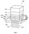
図1には種々異なる実施例にしたがい、例えば発光電子素子100のような電子素子100が示されている。
FIG. 1 shows an
電子素子100は、種々異なる実施例において、有機発光ダイオード(OLED,organic light emitting diode)として、有機フォトダイオード(OPD,organic photodiode)として、有機太陽電池(OSC,organic solar cell)として、または有機トランジスタとして、例えば有機薄膜トランジスタ(OTFT,organic thin film transistor)として形成することができる。発光電子素子100は、種々異なる実施例において集積回路の一部分とすることが可能である。さらに多数の(例えば発光)電子素子100を設けることができ、これらは例えば共通の1つのケーシング内に収容される。
In various embodiments, the
(例えば発光)電子素子100は、基板102を有し得る。例えば基板102は、電子素子または層、例えばオプトエレクトロニクス素子用の支持体素子として使用することができる。例えば基板102は、ガラス、石英および/または半導体材料または他の任意の有利な材料を有し得るかまたはこのような材料から構成することが可能である。さらに基板102は、1つのプラスチックシート、または、1つまたは複数のプラスチックシートを備えた1つの積層体を有するか、またはこのようなものから構成することが可能である。このプラスチックは、1つまたは複数のポリオレフィン(例えば、低密度または高密度のポリエチレン(PE)またはポリプロピレン(PP))を有するかまたはこのようなものから構成することが可能である。さらに上記のプラスチックは、ポリ塩化ビニル(PVC)、ポリスチロール(PS)、ポリエステルおよび/またはポリカーボネート(PC)、ポリエチレンテレフタラート(PET)、ポリエーテルサルフォン(PES)および/またはポリエチレンナフタレート(PEN)を有するかまたはこれらから構成することができる。さらに基板102は、例えば金属製シートを有することができ、例えば、アルミニウムシート、特殊鋼シート、銅シートまたはこれらの組み合わせまたはシート積層体を有し得る。基板102は、上で挙げた材料のうちの1つまたはいくつかを有し得る。基板102は、透明または部分的に透明に実施することができ、または不透明に実施することも可能である。
The (eg light emitting)
基板102上またはこれを覆って第1電極層104を被着することができる。第1電極104(以下では下側電極104とも称する)は、導電性材料から構成するかまたはこのようなものとすることが可能であり、例えば、金属または透明導電酸化物(TCO,transparent conductive oxide)から、または同じ金属または種々異なる金属および/または同じTCOまたは種々異なるTCOの複数の層からなる積層体から構成するかまたはこのようなものとすることが可能である。透明導電酸化物は、例えば、すず酸化物、亜鉛酸化物、カドミウム酸化物、チタン酸化物、インジウム酸化物またはインジウムすず酸化物(ITO)のような透明かつ導電性の材料である。例えばZnO,SnO2またはIn2O3のような2元の金属酸素化合物の他に、例えばZn2SnO4,CdSnO3,ZnSnO3,MgIn2O4,GaInO3,Zn2In2O5またはIn4Sn3O12のような3元の金属酸素化合物、または種々異なる透明導電酸化物の混合物もTCOのグループに属する。さらにTCOは、必ずしも化学量論的な組成に相応する必要はなく、さらにpドーピングまたはnドーピングすることができる。第1電極104は、アノードとして、すなわち正孔注入材料として形成することが可能である。
A
種々異なる実施例において第1電極104は、TCOの層上の金属の層の組み合わせまたはこの逆の組み合わせの積層体によって構成することができる。1つの例は、インジウムすず酸化層(ITO)上に被着される銀層(ITO上のAg)である。種々異なる実施例において第1電極104は、金属(例えばAg,Pt,Au,Mg)を有することができるかまたは上記の材料の金属合金(例えばAgMg合金)を有することができる。種々異なる実施例において第1電極104は、AlZnOまたは類似の材料を有し得る。
In different embodiments, the
種々異なる実施形態において第1電極104は、例えば、カソード材料、すなわち電子注入材料として使用可能な金属を有することができる。カソード材料として、殊に、例えばAl,Ba,In,Ag,Au,Mg,CaまたはLi、ならびに、これらの材料の化合物、組み合わせまたは合金を種々異なる実施例において使用することができる。
In various embodiments, the
発光電子素子100をボトムエミッタとして構成する場合、第1電極104は、例えば、約25nm以下の層厚を有することができ、例えば、約20nm以下の層厚、例えば約18nm以下の層厚を有することができる。さらに第1電極104は、例えば約10nm以上の層厚を、例えば約15nm以上の層厚を有し得る。種々異なる実施例において第1電極104は、約10nmから約25nmの範囲の層厚を、例えば約10nmから約18nmの範囲の層厚を、例えば約15nmから約18nmの範囲の層厚を有することができる。
When the light emitting
発光電子素子100をトップエミッタとして構成する場合、第1電極104は、例えば約40nm以上の層厚を、例えば約50nm以上の層厚を有し得る。
When the light emitting
さらに(例えば発光)電子素子100は、第1電極104上にまたはこれ覆って被着されているかまたは被着される有機機能層構造体106を有することができる。
Further (e.g., light emitting)
有機機能層構造体106は、例えば、蛍光性および/またはりん光性のエミッタを備えた1つまたは複数のエミッタ層108と、1つまたは複数の正孔ガイド層110を有し得る。
The organic
1つまたは複数のエミッタ層108についての種々異なる実施例の電子素子に使用可能なエミッタ材料の例には、ポリフルオレン、ポリチオフェンおよびポリフェニレン(例えば2−または2.5−置換ポリpフェニルビニレン)などの誘導体、ならびに金属錯体、例えば、青色のりん光性のFIrPic(ビス(3,5−ジフルオロ−2−(2−ピリジル)フェニル−(2−カルボキシピリジル)−イリジウムIII)のようなイリジウム錯体、緑色のりん光性のIr(ppy)3(トリス(2−フェニルピリジン)イリジウムIII)、赤色のりん光性Ru(dtb-bpy)3*2(PF6)(トリス[4,4'−ジ−t−ブチル−(2,2’)−ビピリジン]ルテニウム(III)錯体)ならびに青色の蛍光性のDPAVBi(4,4−ビス[4−(ジ−p−トリラミノ)スチリル]ビフェニル)、緑色の蛍光性のTTPA(9,10−ビス[N,N−ジ−(p−トリル)−アミノ]アントラセン)および赤色の蛍光性のDCM2(4−ジシアノメチレン)−2−メチル−6−ジュロリジル−9−エニル−4H−ピラン)のような有機または有機金属化合物が非ポリマエミッタとして含まれている。このような非ポリマエミッタは、例えば、熱蒸着によってデポジット可能である。さらに、例えばスピンコーティングなどの殊に湿式化学法によってデポジット可能なポリマエミッタを使用可能である。 Examples of emitter materials that can be used in electronic devices of different embodiments for one or more emitter layers 108 include polyfluorene, polythiophene, and polyphenylene (eg, 2- or 2.5-substituted poly p-phenyl vinylene). As well as metal complexes, for example iridium complexes such as blue phosphorescent FIrPic (bis (3,5-difluoro-2- (2-pyridyl) phenyl- (2-carboxypyridyl) -iridium III), Green phosphorescent Ir (ppy) 3 (Tris (2-phenylpyridine) iridium III), red phosphorescent Ru (dtb-bpy) 3 * 2 (PF 6 ) (Tris [4,4'-di -T-butyl- (2,2 ′)-bipyridine] ruthenium (III) complex) as well as blue fluorescent DPAVBi (4,4-bis [4- (di-p-trilamino) styryl] biphenyl) Green fluorescent TTPA (9,10-bis [N, N-di- (p-tolyl) -amino] anthracene) and red fluorescent DCM2 (4-dicyanomethylene) -2-methyl-6-julolidyl Organic or organometallic compounds such as (-9-enyl-4H-pyran) are included as non-polymer emitters. Such non-polymer emitters can be deposited, for example, by thermal evaporation. Furthermore, it is possible to use polymer emitters that can be deposited, in particular by wet chemical methods, such as spin coating.
上記のエミッタ材料は、適当な手法でマトリクス材料に埋め込むことができる。 The above emitter material can be embedded in the matrix material by any suitable technique.
電子素子100が白色光を放射するように電子素子100の1つまたは複数のエミッタ層108のエミッタ材料を選択することができる。1つまたは複数のエミッタ層108は、複数の異なる色(例えば、青色および黄色、または青色、緑色および赤色)を放射するエミッタ材料を有することができ、また択一的には1つまたは複数のエミッタ層108は、複数の部分層から形成することも可能であり、青色の蛍光エミッタ層108または青色のりん光エミッタ層108、緑色の蛍光エミッタ層108および赤色の蛍光エミッタ層108から形成することも可能である。これらの種々異なる色を混ぜることにより、白色の色印象を有する光の放射が得られる。択一的にはこれらの層によって形成される1次放射のビーム路に、1次ビームの少なくとも一部を吸収して別の波長の2次ビームを放射する変換材料を配置することも可能であり、これによって(まだ白色でない)1次ビームから、1次ビームと2次ビームとを組み合わせることによって白色の色印象が得られるのである。
The emitter material of one or more emitter layers 108 of the
有機機能層構造体106は一般的に1つまたは複数の機能層を有することができる。この1つまたは複数の機能層は、有機ポリマ、有機オリゴマ、有機モノマ、有機非ポリマ小分子("small molecues")またはこれらの材料の組み合わせを有し得る。例えば、有機機能層構造体106は、正孔輸送層110として実施される1つまたは複数の機能層を有し得るため、例えば、OLEDの場合にエレクトロルミネセンス層またはエレクトロルミネセンス領域に効果的に正孔を注入することができる。正孔輸送層110用の材料として、例えば、第3アミン、カルバゾル誘導体、導電性ポリアニリンまたはポリエチレンジオキシチオフェンを使用可能である。種々異なる実施例において上記の1つまたは複数の機能層は、エレクトロルミネセンス層として実施することができる。
The organic
種々異なる実施例において正孔輸送層110は、第1電極104上にまたはこれを覆って被着することができ、例えばデポジットすることができ、またエミッタ層108は正孔輸送層110上にまたはこれに覆って被着する、例えばデポジットすることができる。
In different embodiments, the
電子素子100は一般的に、電子素子100の機能性をさらに改善しひいてはその効率をさらに改善するために使用される別の有機機能層を有し得る。
The
発光電子素子100は、「ボトムエミッタ」および/または「トップエミッタ」として実施することができる。
The light emitting
種々異なる実施例において、有機機能層構造体106は、最大で約1.5μm、例えば最大で約1.2μm、例えば最大で約1μm、例えば最大で約800nm、例えば最大で約500nm、例えば最大で約400nm、例えば最大で約300nmの層厚を有し得る。種々異なる実施例において有機機能層構造体106は、例えば、上下に直接配置される複数のOLEDの積層体を有することができ、各OLEDは、例えば最大で約1.5μmの層厚、例えば最大で約1.2μmの層厚、例えば最大で約1μmの層厚、例えば最大で約800nmの層厚、例えば最大で約500nmの層厚、例えば最大で約400nmの層厚、例えば最大で約300nmの層厚を有し得る。種々異なる実施例において有機機能層構造体106は、例えば、上下に直接配置される3つまたは4つのOLEDの積層体を有することができ、この場合、例えば、有機機能層構造体106は、最大で約3μmの層厚を有し得る。
In various embodiments, the organic
有機機能層構造体106上にまたはこれを覆って、第2電極112を被着することができる。
A
第2電極112は、第2電極112上にまたはこれを覆って被着される誘電体層114と、有機機能層構造体106とが光結合されるように構成することができる。第2電極112は、有機機能層構造体106から放射されるビームに対して半透明に構成することができる。種々異なる実施例において、第2電極112は、有機機能層構造体106と誘電体層114との間の十分な結合強度(第2電極112の層厚が大きくなればなるほど結合強度は小さくなる)と、発光素子100の達成可能な効率(第2電極112の層厚が大きくなればなるほど効率は高くなる)およびこれに伴う色再現指標との間で、所望の妥協が選択されるような層厚を有することができる。種々異なる実施例において第2電極112は、第1電極104と同じ材料を有するかまたはこの材料から構成することができ、ここでは種々異なる実施例において金属が殊に有利である。
The
種々異なる実施例において第2電極112は、例えば約50nm以下の層厚、例えば約45nm以下の層厚、例えば約40nm以下の層厚、例えば約35nm以下の層厚、例えば約30nm以下の層厚、例えば約25nm以下の層厚、例えば約20nm以下の層厚、例えば約15nm以下の層厚、例えば約10nm以下の層厚を有し得る。
In various embodiments, the
第2電極112上またはこれを覆って(以下では(透明)中間層とも称する)誘電体層114が被着されるかまたは被着されていることが可能である。
A
誘電体層114は、380nmから780nmの波長領域の少なくとも1つの部分領域のビームに対して透過な層とすることができる。例えば、単色発光電子素子または放射スペクトルが制限された電子素子を提供しようとする場合には、誘電体層114が、所望の単色光の波長領域の少なくとも1つの部分領域におけるビームに対して少なくとも透過性を有するか、または上記の制限された放射スペクトルに対して透過性を有するかで十分である。
The
種々異なる実施例において誘電体層114は、ALD法によってデポジットされ、これによって誘電体層114は、原子層エピタキシ層として構成される。種々異なる実施例において誘電体層114は、約50nmから約2μmの範囲の層厚で、例えば約70nmから約200nmの範囲で、例えば約100nmから約120nmの範囲でデポジットされる。この層厚においてカプセリング作用が保証され、例えば結合形マイクロキャビティの厚さを極めて正確に調整することができる。誘電体層114は、例えばSiO2,Si3N4,SiON(これらの材料は、例えばCVD法によってデポジットされる),Al2O3;ZrO2; TiO2;Ta2O5;SiO2;ZnOおよび/またはHfO2(これらの材料は例えばALD法によってデポジットされる)などのような材料または材料の混合物または材料からなる層の積層体またはこれらの材料の組み合わせを有し得る。
In different embodiments, the
誘電体層114上またはこれを覆って反射層構造116が被着されているかまたはこれを被着することができる。
A
反射層構造体116は、第1電極102と同じ材料から構成することができ、ここで層厚は、発光電子素子100がトップエミッタとして構成される場合に、反射層構造体116が、例えば約25nm以下の層厚、例えば20nm以下の層厚、例えば18nm以下の層厚を有し得るように選択することができる。さらに第1電極104は、例えば約10nm以上の層厚、例えば約15nm以上の層厚を有し得る。種々異なる実施例において、反射層構造体116は、約10nmから約25nmの範囲の層厚を有することができ、例えば約10nmから約18nmの範囲の層厚を、例えば約15nmから約18nmの範囲の層厚を有し得る。
The
発光電子素子100がボトムエミッタとして構成される場合、反射層構造体116は、例えば約40nm以上の層厚、例えば約50nm以上の層厚を有し得る。
When the light emitting
反射層構造体116は、1つまたは複数のミラーを有し得る。反射層構造体116が複数のミラーを有する場合、各ミラーは各誘電体層によって互いに分離される。
The
図1に示した電子素子100は、光ビーム118によってシンボリックに示されているようにボトムエミッタとして構成されている。
The
発光電子素子100を作製する際のALD法およびCVD法により、ALD法を用いることによって極めて正確に調整可能な層厚で誘電体層114をデポジットすることができる。種々異なる実施例において、容易にわかるように、互いに光結合される2つのマイクロキャビティを有する慣用の有機発光ダイオードにおいて設けられる第2有機層を、密度の高い1つの誘電体層によって置き換えることができる。
The
種々異なる実施例において、上記のデポジットされる誘電体層114はカプセリング作用を有しているため、構成される電子素子および例えば有機機能層構造体106は、空気または水などの浸入から保護される。
In different embodiments, the deposited
技術的な条件に起因して、ALD法は、有機材料の蒸着に比べて格段に層厚のばらつきが小さく、これにより、種々異なる実施例によれば、例えば結合形マイクロキャビティOLEDを商品として利用可能になる。例えば、これにより、有機層の層厚のばらつきも、例えば誘電体層114の層厚の調整によって補償することができ、これによって商品としての装置における歩留まりを高めることができる。
Due to technical conditions, the ALD method has a much smaller variation in layer thickness compared to the vapor deposition of organic materials, so that, for example, according to different embodiments, coupled microcavity OLEDs are used as commercial products. It becomes possible. For example, it is possible to compensate for variations in the layer thickness of the organic layer, for example, by adjusting the layer thickness of the
種々異なる実施例において、種々異なる実施例による複数または多数の発光電子100を用いて照明装置または表示装置(ディスプレイ)を提供することができる。この照明装置または表示装置は、大面積に構成されるアクティブな発光面を有し得る。種々異なる実施例において「大面積」とは、上記の発光面が、数平方ミリメートル以上、例えば数平方センチメート以上、例えば数平方デシメートル以上の面積を有することを意味し得る。
In different embodiments, a lighting device or display device (display) can be provided using multiple or multiple
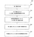
図2には流れ図200が示されており、ここでは発光電子素子を作製するための方法が1つの実施例にしたがって示されている。
FIG. 2 shows a
202では第1電極が形成され、また204では有機機能層構造体が第1電極上にまたはこれを覆って形成される。さらに206では第2電極が有機機能層構造体上にまたはこれを覆って形成され、208では誘電体層が第2電極上にまたはこれを覆って形成される。最後に210では反射層構造体が上記の誘電体層上にまたはこれを覆って形成される。 In 202, a first electrode is formed, and in 204, an organic functional layer structure is formed on or over the first electrode. Further, at 206, a second electrode is formed on or over the organic functional layer structure, and at 208, a dielectric layer is formed on or over the second electrode. Finally, at 210, a reflective layer structure is formed on or over the dielectric layer.
Claims (16)
該電子素子は、
− 第1電極(104)と、
− 該第1電極(104)上のまたは当該第1電極(104)を覆う有機機能層構造体(106)と、
− 該有機機能層構造体(106)上のまたは当該有機機能層構造体(106)を覆う第2電極(112)と、
− 当該第2電極(112)上のまたは当該第2電極(112)を覆う誘電体層(114)と、
− 当該誘電体層(114)上のまたは当該誘電体層(114)を覆う反射層構造体(116)とを有しており、
前記有機機能層構造体(106)は、前記第1電極(104)と前記第2電極(112)との間で第1マイクロキャビティを構成し、
前記誘電体層(114)は、前記第2電極(112)と前記反射構造体(116)との間で第2マイクロキャビティを構成する、
ことを特徴とする電子素子(100)。 In the electronic device (100),
The electronic element is
-A first electrode (104);
-An organic functional layer structure (106) on or covering the first electrode (104);
-A second electrode (112) on or covering said organic functional layer structure (106);
-A dielectric layer (114) on or covering said second electrode (112);
A reflective layer structure (116) on or covering the dielectric layer (114);
The organic functional layer structure (106) forms a first microcavity between the first electrode (104) and the second electrode (112),
The dielectric layer (114) forms a second microcavity between the second electrode (112) and the reflective structure (116).
An electronic device (100) characterized by the above.
前記第1マイクロキャビティが前記第2電極(112)を介して前記第2マイクロキャビティに光結合されるように前記第2電極(112)が構成されている、
ことを特徴とする電子素子(100)。 The electronic device (100) according to claim 1,
The second electrode (112) is configured such that the first microcavity is optically coupled to the second microcavity via the second electrode (112).
An electronic device (100) characterized by the above.
前記第2電極(112)は、前記有機機能層構造体(106)から放射されるビームに対して半透明である、
ことを特徴とする電子素子(100)。 The electronic device (100) according to claim 2,
The second electrode (112) is translucent to the beam emitted from the organic functional layer structure (106).
An electronic device (100) characterized by the above.
前記誘電体層(114)は、380nmから780nmの波長領域の少なくとも1つの部分領域におけるビームに対して透明である、
ことを特徴とする電子素子(100)。 The electronic device (100) according to any one of claims 1 to 3,
The dielectric layer (114) is transparent to the beam in at least one partial region of the wavelength region from 380 nm to 780 nm;
An electronic device (100) characterized by the above.
前記誘電体層(114)は、つぎの方法のうちの1つによって被着されている、すなわち、
− 化学気相デポジット法
− 物理気相デポジット法
− スピンコーティング法
− 印刷法
− スキージ法
− スプレー法
− ディップコーティング法のいずれかによって被着されている、
ことを特徴とする電子素子(100)。 In the electronic device (100) according to any one of claims 1 to 4,
The dielectric layer (114) is deposited by one of the following methods:
-Chemical vapor deposition method-physical vapor deposition method-spin coating method-printing method-squeegee method-spray method-applied by any of dip coating method,
An electronic device (100) characterized by the above.
前記誘電体層(114)は、原子層エピタキシ層である、
ことを特徴とする電子素子(100)。 Electronic device (100) according to any one of claims 1 to 5,
The dielectric layer (114) is an atomic layer epitaxy layer,
An electronic device (100) characterized by the above.
前記誘電体層(114)は、約50nmから約2μmの範囲の、有利には約70nmから約200nmの範囲の層厚を有する、
ことを特徴とする電子素子(100)。 The electronic device (100) according to any one of claims 1 to 6,
The dielectric layer (114) has a layer thickness in the range of about 50 nm to about 2 μm, preferably in the range of about 70 nm to about 200 nm.
An electronic device (100) characterized by the above.
前記誘電体層(114)は、SiO2,Si3N4,SiON,Al2O3,ZrO2,TiO2,Ta2O5,SiO2,ZnOおよびHfO2からなるグループから選択される材料または当該材料の混合物または当該材料の層の積層体を有するかまたは当該材料の組み合わせを有する、
ことを特徴とする電子素子(100)。 In the electronic device (100) according to any one of claims 1 to 7,
The dielectric layer (114) is a material selected from the group consisting of SiO 2 , Si 3 N 4 , SiON, Al 2 O 3 , ZrO 2 , TiO 2 , Ta 2 O 5 , SiO 2 , ZnO and HfO 2. Or a mixture of the materials or a stack of layers of the materials or a combination of the materials,
An electronic device (100) characterized by the above.
当該方法は、
− 第1電極(104)を形成するステップ(202)と、
− 当該第1電極(104)上にまたは当該第1電極(104)を覆って有機機能層構造体(106)を形成するステップ(204)と、
− 当該有機機能層構造体(106)上にまたは当該有機機能層構造体(106)を覆って第2電極(112)を形成するステップ(206)と、
− 当該第2電極(112)上にまたは当該第2電極(112)を覆って誘電体層(114)を形成するステップ(208)と、
− 前記有機機能層構造体(106)が前記第1電極(104)と前記第2電極(112)との間で第1マイクロキャビティを構成するように、かつ、前記誘電体層(114)が、前記第2電極(112)と前記反射層構造体(116)との間で第2マイクロキャビテを構成するように、
前記誘電体層(114)上にまたは当該誘電体層(114)を覆って反射層構造体(116)を形成するステップとを有する、
ことを特徴とする、電子素子(100)を作製する方法。 In a method (200) for making an electronic device (100),
The method is
-Forming a first electrode (104) (202);
-Forming (204) an organic functional layer structure (106) on or over the first electrode (104);
-Forming a second electrode (112) on the organic functional layer structure (106) or covering the organic functional layer structure (106) (206);
-Forming (208) a dielectric layer (114) on or over the second electrode (112);
The organic functional layer structure (106) forms a first microcavity between the first electrode (104) and the second electrode (112), and the dielectric layer (114) In order to form a second microcavity between the second electrode (112) and the reflective layer structure (116),
Forming a reflective layer structure (116) on or over the dielectric layer (114).
A method of manufacturing an electronic device (100), characterized in that
前記第1マイクロキャビティと前記第2マイクロキャビティとが光結合されるように前記第2電極(112)を構成する、
ことを特徴とする方法。 The method of claim 9, wherein
Configuring the second electrode (112) such that the first microcavity and the second microcavity are optically coupled;
A method characterized by that.
前記有機機能層構造体(106)から放射されるビームに対して半透明に前記第2電極(112)を構成する、
ことを特徴とする方法。 The method of claim 10, wherein
The second electrode (112) is configured to be translucent to the beam emitted from the organic functional layer structure (106).
A method characterized by that.
380nmから780nmの波長領域の少なくとも1つの部分領域におけるビームに対して透明である層として前記誘電体層(114)を形成する、
ことを特徴とする方法。 12. The method according to any one of claims 9 to 11, wherein
Forming the dielectric layer (114) as a layer that is transparent to the beam in at least one partial region of the wavelength region from 380 nm to 780 nm;
A method characterized by that.
前記誘電体層(114)をつぎの方法のうちの1つによって被着する、すなわち、
− 化学気相デポジット法
− 物理気相デポジット法
− スピンコーティング法
− 印刷法
− スキージ法
− スプレー法
− ディップコーティング法
のいずれか1つの方法によって被着する、
ことを特徴とする方法。 The method according to any one of claims 9 to 12,
The dielectric layer (114) is deposited by one of the following methods:
-Chemical vapor deposition method-Physical vapor deposition method-Spin coating method-Printing method-Squeegee method-Spray method-Dip coating method
A method characterized by that.
前記誘電体層(114)を原子層エピタキシ法によって被着する、
ことを特徴とする方法。 The method according to any one of claims 9 to 13, wherein
Depositing said dielectric layer (114) by atomic layer epitaxy;
A method characterized by that.
約50nmから約2μmの範囲の、有利には約70nmから約200nmの範囲の層厚で前記誘電体層(114)を形成する、
ことを特徴とする方法。 15. The method according to any one of claims 9 to 14, wherein
Forming said dielectric layer (114) with a layer thickness in the range of about 50 nm to about 2 μm, preferably in the range of about 70 nm to about 200 nm;
A method characterized by that.
前記誘電体層(114)を、SiO2,Si3N4,SiON,Al2O3,ZrO2,TiO2,Ta2O5,SiO2,ZnOおよびHfO2からなるグループから選択される材料または当該材料の混合物または当該材料の層の積層体から形成するか、または当該材料の組み合わせとする、
ことを特徴とする方法。 The method according to any one of claims 9 to 15, wherein
The material dielectric layer (114), which is selected from the group consisting of SiO 2, Si 3 N 4, SiON, Al 2 O 3, ZrO 2, TiO 2, Ta 2 O 5, SiO 2, ZnO and HfO 2 Or formed from a mixture of the materials or a stack of layers of the materials, or a combination of the materials,
A method characterized by that.
Applications Claiming Priority (3)
| Application Number | Priority Date | Filing Date | Title |
|---|---|---|---|
| DE102010042982A DE102010042982A1 (en) | 2010-10-27 | 2010-10-27 | Electronic component and method for manufacturing an electronic component |
| DE102010042982.1 | 2010-10-27 | ||
| PCT/EP2011/067643 WO2012055694A1 (en) | 2010-10-27 | 2011-10-10 | Electronic component and method for producing an electronic component |
Publications (2)
| Publication Number | Publication Date |
|---|---|
| JP2013545230A true JP2013545230A (en) | 2013-12-19 |
| JP2013545230A5 JP2013545230A5 (en) | 2014-11-20 |
Family
ID=45531621
Family Applications (1)
| Application Number | Title | Priority Date | Filing Date |
|---|---|---|---|
| JP2013535348A Pending JP2013545230A (en) | 2010-10-27 | 2011-10-10 | Electronic device and method for manufacturing electronic device |
Country Status (7)
| Country | Link |
|---|---|
| US (1) | US20130270536A1 (en) |
| EP (1) | EP2633568A1 (en) |
| JP (1) | JP2013545230A (en) |
| KR (1) | KR20130086052A (en) |
| CN (1) | CN103210518A (en) |
| DE (1) | DE102010042982A1 (en) |
| WO (1) | WO2012055694A1 (en) |
Cited By (1)
| Publication number | Priority date | Publication date | Assignee | Title |
|---|---|---|---|---|
| JP2020113384A (en) * | 2019-01-09 | 2020-07-27 | セイコーエプソン株式会社 | Organic electroluminescent device, method for manufacturing organic electroluminescent device, head-mounted display, and electronic apparatus |
Families Citing this family (5)
| Publication number | Priority date | Publication date | Assignee | Title |
|---|---|---|---|---|
| CN103545449A (en) * | 2012-07-10 | 2014-01-29 | 群康科技(深圳)有限公司 | Organic light emitting diode (OLED), display panel with OLED and display equipment with OLED |
| CN109427988B (en) * | 2017-08-21 | 2021-02-12 | 上海和辉光电股份有限公司 | Display panel and display device |
| CN108365115B (en) * | 2017-08-29 | 2019-07-19 | 广东聚华印刷显示技术有限公司 | Electroluminescent device, display panel and preparation method thereof |
| CN111628102A (en) * | 2020-05-18 | 2020-09-04 | 武汉华星光电半导体显示技术有限公司 | Microcavity electrode structure and organic electroluminescent device |
| CN116487401A (en) * | 2022-01-17 | 2023-07-25 | 华为技术有限公司 | Display panel and electronic device |
Citations (3)
| Publication number | Priority date | Publication date | Assignee | Title |
|---|---|---|---|---|
| JP2005071919A (en) * | 2003-08-27 | 2005-03-17 | Hitachi Ltd | Highly efficient organic light emitting element |
| JP2008047340A (en) * | 2006-08-11 | 2008-02-28 | Dainippon Printing Co Ltd | Organic electroluminescence device |
| JP2009258406A (en) * | 2008-04-17 | 2009-11-05 | Sumitomo Metal Mining Co Ltd | Dielectric multilayer film mirror and method of manufacturing the same |
Family Cites Families (11)
| Publication number | Priority date | Publication date | Assignee | Title |
|---|---|---|---|---|
| CA2277654A1 (en) * | 1999-07-19 | 2001-01-19 | Luxell Technologies Inc. | Electroluminescent display packaging and method therefor |
| WO2003105248A1 (en) * | 2002-06-11 | 2003-12-18 | Luxell Technologies Inc. | Oled display with contrast enhancing interference members |
| KR100567179B1 (en) * | 2002-09-30 | 2006-04-03 | 가부시키가이샤 도요다 지도숏키 | Light-emitting device, display unit and lighting unit |
| US20050093437A1 (en) * | 2003-10-31 | 2005-05-05 | Ouyang Michael X. | OLED structures with strain relief, antireflection and barrier layers |
| TWI231723B (en) * | 2004-04-16 | 2005-04-21 | Ind Tech Res Inst | Organic electroluminescence display device |
| JP4363365B2 (en) * | 2004-07-20 | 2009-11-11 | 株式会社デンソー | Color organic EL display and manufacturing method thereof |
| US20060109397A1 (en) * | 2004-11-24 | 2006-05-25 | Organic Lighting Technologies Llc | Organic light emitting diode backlight inside LCD |
| KR100715500B1 (en) * | 2004-11-30 | 2007-05-07 | (주)케이디티 | Light source with micro-cavity organic light emitting diode and photoluminescent layer |
| US20060197436A1 (en) * | 2005-03-01 | 2006-09-07 | Sharp Laboratories Of America, Inc. | ZnO nanotip electrode electroluminescence device on silicon substrate |
| US7728512B2 (en) * | 2007-03-02 | 2010-06-01 | Universal Display Corporation | Organic light emitting device having an external microcavity |
| FR2933538B1 (en) * | 2008-07-07 | 2012-09-21 | Commissariat Energie Atomique | DISPLAY, LIGHTING OR SIGNALING ELECTROLUMINESCENT DEVICE AND METHOD FOR MANUFACTURING THE SAME |
-
2010
- 2010-10-27 DE DE102010042982A patent/DE102010042982A1/en not_active Withdrawn
-
2011
- 2011-10-10 EP EP11772918.6A patent/EP2633568A1/en not_active Ceased
- 2011-10-10 CN CN2011800518797A patent/CN103210518A/en active Pending
- 2011-10-10 JP JP2013535348A patent/JP2013545230A/en active Pending
- 2011-10-10 KR KR1020137013568A patent/KR20130086052A/en not_active Application Discontinuation
- 2011-10-10 US US13/881,761 patent/US20130270536A1/en not_active Abandoned
- 2011-10-10 WO PCT/EP2011/067643 patent/WO2012055694A1/en active Application Filing
Patent Citations (3)
| Publication number | Priority date | Publication date | Assignee | Title |
|---|---|---|---|---|
| JP2005071919A (en) * | 2003-08-27 | 2005-03-17 | Hitachi Ltd | Highly efficient organic light emitting element |
| JP2008047340A (en) * | 2006-08-11 | 2008-02-28 | Dainippon Printing Co Ltd | Organic electroluminescence device |
| JP2009258406A (en) * | 2008-04-17 | 2009-11-05 | Sumitomo Metal Mining Co Ltd | Dielectric multilayer film mirror and method of manufacturing the same |
Cited By (1)
| Publication number | Priority date | Publication date | Assignee | Title |
|---|---|---|---|---|
| JP2020113384A (en) * | 2019-01-09 | 2020-07-27 | セイコーエプソン株式会社 | Organic electroluminescent device, method for manufacturing organic electroluminescent device, head-mounted display, and electronic apparatus |
Also Published As
| Publication number | Publication date |
|---|---|
| CN103210518A (en) | 2013-07-17 |
| US20130270536A1 (en) | 2013-10-17 |
| WO2012055694A1 (en) | 2012-05-03 |
| KR20130086052A (en) | 2013-07-30 |
| DE102010042982A1 (en) | 2012-05-03 |
| EP2633568A1 (en) | 2013-09-04 |
Similar Documents
| Publication | Publication Date | Title |
|---|---|---|
| US9530962B2 (en) | Patterning method for OLEDs | |
| US9252378B2 (en) | Organic light-emitting component | |
| US9224985B2 (en) | Optoelectronic component | |
| KR101084271B1 (en) | Organic light emitting diode device and method for manufacturing the same | |
| US9130196B2 (en) | Light-emitting component and method for producing a light-emitting component | |
| US20150027541A1 (en) | Electronic component with moisture barrier layer | |
| JP6038295B2 (en) | ORGANIC LIGHT EMITTING ELEMENT AND METHOD FOR PRODUCING ORGANIC LIGHT EMITTING ELEMENT | |
| KR101650029B1 (en) | Light-emitting components and method for producing a light-emitting component | |
| JP2013545230A (en) | Electronic device and method for manufacturing electronic device | |
| US10361396B2 (en) | Optoelectronic component with multilayer encapsulant CTE matched to electrode | |
| US10454050B2 (en) | Organic light-emitting device | |
| US20140225086A1 (en) | Organic light-emitting component and method for producing an organic light-emitting component | |
| KR20140021052A (en) | Optoelectronic component and method for producing an optoelectronic component | |
| WO2016188042A1 (en) | Electroluminescent component, manufacturing method therefor, display substrate, and display device | |
| KR102080630B1 (en) | Light-emitting component and method for producing a light-emitting component | |
| KR20140048266A (en) | Light-emitting component and method for producing a light-emitting component | |
| US9818982B2 (en) | Optoelectronic assembly and method for producing an optoelectronic assembly | |
| KR20170030637A (en) | Optoelectronic component and a method for producing an optoelectronic component | |
| US20130270542A1 (en) | Method for producing an optoelectronic component and optoelectronic component | |
| US20170005290A1 (en) | Optoelectronic component and method for producing an optoelectronic component | |
| WO2012105333A1 (en) | Production method for organic electroluminescence element and organic electroluminescence element | |
| KR20120025148A (en) | Passive matrix organic light emitting diode having anti-oxidant and anti-scattering layer and its manufacturing method |
Legal Events
| Date | Code | Title | Description |
|---|---|---|---|
| A131 | Notification of reasons for refusal |
Free format text: JAPANESE INTERMEDIATE CODE: A131 Effective date: 20140602 |
|
| A601 | Written request for extension of time |
Free format text: JAPANESE INTERMEDIATE CODE: A601 Effective date: 20140828 |
|
| A602 | Written permission of extension of time |
Free format text: JAPANESE INTERMEDIATE CODE: A602 Effective date: 20140904 |
|
| A521 | Request for written amendment filed |
Free format text: JAPANESE INTERMEDIATE CODE: A523 Effective date: 20141002 |
|
| A524 | Written submission of copy of amendment under article 19 pct |
Free format text: JAPANESE INTERMEDIATE CODE: A524 Effective date: 20141002 |
|
| A02 | Decision of refusal |
Free format text: JAPANESE INTERMEDIATE CODE: A02 Effective date: 20141027 |