KR20130076790A - Method for manufacturing silicon carbide semiconductor device and apparatus for manufacturing silicon carbide semiconductor device - Google Patents
Method for manufacturing silicon carbide semiconductor device and apparatus for manufacturing silicon carbide semiconductor device Download PDFInfo
- Publication number
- KR20130076790A KR20130076790A KR1020127010182A KR20127010182A KR20130076790A KR 20130076790 A KR20130076790 A KR 20130076790A KR 1020127010182 A KR1020127010182 A KR 1020127010182A KR 20127010182 A KR20127010182 A KR 20127010182A KR 20130076790 A KR20130076790 A KR 20130076790A
- Authority
- KR
- South Korea
- Prior art keywords
- oxide film
- silicon carbide
- carbide semiconductor
- forming
- semiconductor device
- Prior art date
Links
- 239000004065 semiconductor Substances 0.000 title claims abstract description 186
- 238000004519 manufacturing process Methods 0.000 title claims abstract description 88
- 238000000034 method Methods 0.000 title claims abstract description 72
- HBMJWWWQQXIZIP-UHFFFAOYSA-N silicon carbide Chemical compound [Si+]#[C-] HBMJWWWQQXIZIP-UHFFFAOYSA-N 0.000 title claims description 214
- 229910010271 silicon carbide Inorganic materials 0.000 title claims description 213
- 239000012298 atmosphere Substances 0.000 claims abstract description 82
- 230000008569 process Effects 0.000 claims abstract description 36
- 239000007789 gas Substances 0.000 claims description 71
- 230000015572 biosynthetic process Effects 0.000 claims description 42
- VEXZGXHMUGYJMC-UHFFFAOYSA-N Hydrochloric acid Chemical compound Cl VEXZGXHMUGYJMC-UHFFFAOYSA-N 0.000 claims description 7
- IXCSERBJSXMMFS-UHFFFAOYSA-N hydrogen chloride Substances Cl.Cl IXCSERBJSXMMFS-UHFFFAOYSA-N 0.000 claims description 7
- 229910000041 hydrogen chloride Inorganic materials 0.000 claims description 7
- 238000000859 sublimation Methods 0.000 claims description 7
- 230000008022 sublimation Effects 0.000 claims description 7
- UFHFLCQGNIYNRP-UHFFFAOYSA-N Hydrogen Chemical compound [H][H] UFHFLCQGNIYNRP-UHFFFAOYSA-N 0.000 claims description 5
- 238000005530 etching Methods 0.000 claims description 5
- SFZCNBIFKDRMGX-UHFFFAOYSA-N sulfur hexafluoride Chemical compound FS(F)(F)(F)(F)F SFZCNBIFKDRMGX-UHFFFAOYSA-N 0.000 claims description 5
- 229960000909 sulfur hexafluoride Drugs 0.000 claims description 5
- TXEYQDLBPFQVAA-UHFFFAOYSA-N tetrafluoromethane Chemical compound FC(F)(F)F TXEYQDLBPFQVAA-UHFFFAOYSA-N 0.000 claims description 5
- XUIMIQQOPSSXEZ-UHFFFAOYSA-N Silicon Chemical compound [Si] XUIMIQQOPSSXEZ-UHFFFAOYSA-N 0.000 claims description 4
- 229910052710 silicon Inorganic materials 0.000 claims description 4
- 239000010703 silicon Substances 0.000 claims description 4
- 235000012431 wafers Nutrition 0.000 description 78
- 239000012535 impurity Substances 0.000 description 54
- 239000002245 particle Substances 0.000 description 46
- 238000004140 cleaning Methods 0.000 description 23
- 239000000758 substrate Substances 0.000 description 23
- 238000005406 washing Methods 0.000 description 14
- 229910052760 oxygen Inorganic materials 0.000 description 13
- QVGXLLKOCUKJST-UHFFFAOYSA-N atomic oxygen Chemical compound [O] QVGXLLKOCUKJST-UHFFFAOYSA-N 0.000 description 11
- 239000001301 oxygen Substances 0.000 description 11
- 230000003647 oxidation Effects 0.000 description 10
- 238000007254 oxidation reaction Methods 0.000 description 10
- 238000010438 heat treatment Methods 0.000 description 9
- IJGRMHOSHXDMSA-UHFFFAOYSA-N Atomic nitrogen Chemical compound N#N IJGRMHOSHXDMSA-UHFFFAOYSA-N 0.000 description 8
- 238000000137 annealing Methods 0.000 description 8
- 238000005498 polishing Methods 0.000 description 7
- 239000000243 solution Substances 0.000 description 7
- XKRFYHLGVUSROY-UHFFFAOYSA-N Argon Chemical compound [Ar] XKRFYHLGVUSROY-UHFFFAOYSA-N 0.000 description 6
- MWUXSHHQAYIFBG-UHFFFAOYSA-N Nitric oxide Chemical compound O=[N] MWUXSHHQAYIFBG-UHFFFAOYSA-N 0.000 description 6
- CBENFWSGALASAD-UHFFFAOYSA-N Ozone Chemical compound [O-][O+]=O CBENFWSGALASAD-UHFFFAOYSA-N 0.000 description 6
- 239000004020 conductor Substances 0.000 description 6
- 230000000903 blocking effect Effects 0.000 description 5
- 239000007791 liquid phase Substances 0.000 description 5
- 238000001020 plasma etching Methods 0.000 description 5
- YCKRFDGAMUMZLT-UHFFFAOYSA-N Fluorine atom Chemical compound [F] YCKRFDGAMUMZLT-UHFFFAOYSA-N 0.000 description 4
- 230000015556 catabolic process Effects 0.000 description 4
- 238000006243 chemical reaction Methods 0.000 description 4
- 238000005229 chemical vapour deposition Methods 0.000 description 4
- 238000010586 diagram Methods 0.000 description 4
- 230000005669 field effect Effects 0.000 description 4
- 229910052731 fluorine Inorganic materials 0.000 description 4
- 239000011737 fluorine Substances 0.000 description 4
- 238000005468 ion implantation Methods 0.000 description 4
- 229910052757 nitrogen Inorganic materials 0.000 description 4
- LIVNPJMFVYWSIS-UHFFFAOYSA-N silicon monoxide Chemical group [Si-]#[O+] LIVNPJMFVYWSIS-UHFFFAOYSA-N 0.000 description 4
- 238000001947 vapour-phase growth Methods 0.000 description 4
- XLYOFNOQVPJJNP-UHFFFAOYSA-N water Substances O XLYOFNOQVPJJNP-UHFFFAOYSA-N 0.000 description 4
- PXHVJJICTQNCMI-UHFFFAOYSA-N Nickel Chemical compound [Ni] PXHVJJICTQNCMI-UHFFFAOYSA-N 0.000 description 3
- VYPSYNLAJGMNEJ-UHFFFAOYSA-N Silicium dioxide Chemical compound O=[Si]=O VYPSYNLAJGMNEJ-UHFFFAOYSA-N 0.000 description 3
- 229910052786 argon Inorganic materials 0.000 description 3
- 150000001875 compounds Chemical class 0.000 description 3
- 238000001312 dry etching Methods 0.000 description 3
- 239000011261 inert gas Substances 0.000 description 3
- 230000014759 maintenance of location Effects 0.000 description 3
- 239000002184 metal Substances 0.000 description 3
- 229910052751 metal Inorganic materials 0.000 description 3
- 230000001590 oxidative effect Effects 0.000 description 3
- 238000000197 pyrolysis Methods 0.000 description 3
- 238000007740 vapor deposition Methods 0.000 description 3
- KRHYYFGTRYWZRS-UHFFFAOYSA-N Fluorane Chemical compound F KRHYYFGTRYWZRS-UHFFFAOYSA-N 0.000 description 2
- QAOWNCQODCNURD-UHFFFAOYSA-N Sulfuric acid Chemical compound OS(O)(=O)=O QAOWNCQODCNURD-UHFFFAOYSA-N 0.000 description 2
- 230000004913 activation Effects 0.000 description 2
- 239000003795 chemical substances by application Substances 0.000 description 2
- 239000000356 contaminant Substances 0.000 description 2
- 238000011109 contamination Methods 0.000 description 2
- 230000006866 deterioration Effects 0.000 description 2
- 239000010408 film Substances 0.000 description 2
- 238000002248 hydride vapour-phase epitaxy Methods 0.000 description 2
- 238000002513 implantation Methods 0.000 description 2
- 230000006872 improvement Effects 0.000 description 2
- 230000007774 longterm Effects 0.000 description 2
- 239000000463 material Substances 0.000 description 2
- 229910044991 metal oxide Inorganic materials 0.000 description 2
- 150000004706 metal oxides Chemical class 0.000 description 2
- 239000012071 phase Substances 0.000 description 2
- 238000005554 pickling Methods 0.000 description 2
- 229910052814 silicon oxide Inorganic materials 0.000 description 2
- 239000000126 substance Substances 0.000 description 2
- 238000006467 substitution reaction Methods 0.000 description 2
- 238000005979 thermal decomposition reaction Methods 0.000 description 2
- 239000010936 titanium Substances 0.000 description 2
- 238000001039 wet etching Methods 0.000 description 2
- BLIQUJLAJXRXSG-UHFFFAOYSA-N 1-benzyl-3-(trifluoromethyl)pyrrolidin-1-ium-3-carboxylate Chemical compound C1C(C(=O)O)(C(F)(F)F)CCN1CC1=CC=CC=C1 BLIQUJLAJXRXSG-UHFFFAOYSA-N 0.000 description 1
- DDFHBQSCUXNBSA-UHFFFAOYSA-N 5-(5-carboxythiophen-2-yl)thiophene-2-carboxylic acid Chemical compound S1C(C(=O)O)=CC=C1C1=CC=C(C(O)=O)S1 DDFHBQSCUXNBSA-UHFFFAOYSA-N 0.000 description 1
- CRWSWMKELFKJMC-UHFFFAOYSA-N CC.F.F.F.F.F.F Chemical compound CC.F.F.F.F.F.F CRWSWMKELFKJMC-UHFFFAOYSA-N 0.000 description 1
- OKTJSMMVPCPJKN-UHFFFAOYSA-N Carbon Chemical compound [C] OKTJSMMVPCPJKN-UHFFFAOYSA-N 0.000 description 1
- MYMOFIZGZYHOMD-UHFFFAOYSA-N Dioxygen Chemical compound O=O MYMOFIZGZYHOMD-UHFFFAOYSA-N 0.000 description 1
- 229910017855 NH 4 F Inorganic materials 0.000 description 1
- 229910018503 SF6 Inorganic materials 0.000 description 1
- 229910004298 SiO 2 Inorganic materials 0.000 description 1
- RTAQQCXQSZGOHL-UHFFFAOYSA-N Titanium Chemical compound [Ti] RTAQQCXQSZGOHL-UHFFFAOYSA-N 0.000 description 1
- WGLPBDUCMAPZCE-UHFFFAOYSA-N Trioxochromium Chemical compound O=[Cr](=O)=O WGLPBDUCMAPZCE-UHFFFAOYSA-N 0.000 description 1
- 239000002253 acid Substances 0.000 description 1
- 239000000853 adhesive Substances 0.000 description 1
- 238000005275 alloying Methods 0.000 description 1
- 239000007864 aqueous solution Substances 0.000 description 1
- 239000012300 argon atmosphere Substances 0.000 description 1
- 229910052799 carbon Inorganic materials 0.000 description 1
- 229910000423 chromium oxide Inorganic materials 0.000 description 1
- 230000003749 cleanliness Effects 0.000 description 1
- 239000008119 colloidal silica Substances 0.000 description 1
- 238000004891 communication Methods 0.000 description 1
- 239000013078 crystal Substances 0.000 description 1
- 238000005520 cutting process Methods 0.000 description 1
- 238000000354 decomposition reaction Methods 0.000 description 1
- 229910003460 diamond Inorganic materials 0.000 description 1
- 239000010432 diamond Substances 0.000 description 1
- 229910001873 dinitrogen Inorganic materials 0.000 description 1
- 229910001882 dioxygen Inorganic materials 0.000 description 1
- 238000007599 discharging Methods 0.000 description 1
- 238000001035 drying Methods 0.000 description 1
- 230000000694 effects Effects 0.000 description 1
- 230000005684 electric field Effects 0.000 description 1
- 238000007716 flux method Methods 0.000 description 1
- 238000010574 gas phase reaction Methods 0.000 description 1
- 239000007792 gaseous phase Substances 0.000 description 1
- 238000000227 grinding Methods 0.000 description 1
- 239000001307 helium Substances 0.000 description 1
- 229910052734 helium Inorganic materials 0.000 description 1
- SWQJXJOGLNCZEY-UHFFFAOYSA-N helium atom Chemical compound [He] SWQJXJOGLNCZEY-UHFFFAOYSA-N 0.000 description 1
- 229910000040 hydrogen fluoride Inorganic materials 0.000 description 1
- QOSATHPSBFQAML-UHFFFAOYSA-N hydrogen peroxide;hydrate Chemical compound O.OO QOSATHPSBFQAML-UHFFFAOYSA-N 0.000 description 1
- 230000006698 induction Effects 0.000 description 1
- 230000001939 inductive effect Effects 0.000 description 1
- 238000002347 injection Methods 0.000 description 1
- 239000007924 injection Substances 0.000 description 1
- 229910052743 krypton Inorganic materials 0.000 description 1
- DNNSSWSSYDEUBZ-UHFFFAOYSA-N krypton atom Chemical compound [Kr] DNNSSWSSYDEUBZ-UHFFFAOYSA-N 0.000 description 1
- 239000010410 layer Substances 0.000 description 1
- 239000007788 liquid Substances 0.000 description 1
- 238000012423 maintenance Methods 0.000 description 1
- UNRFQJSWBQGLDR-UHFFFAOYSA-N methane trihydrofluoride Chemical compound C.F.F.F UNRFQJSWBQGLDR-UHFFFAOYSA-N 0.000 description 1
- 238000012986 modification Methods 0.000 description 1
- 230000004048 modification Effects 0.000 description 1
- 238000001451 molecular beam epitaxy Methods 0.000 description 1
- 239000002052 molecular layer Substances 0.000 description 1
- QKCGXXHCELUCKW-UHFFFAOYSA-N n-[4-[4-(dinaphthalen-2-ylamino)phenyl]phenyl]-n-naphthalen-2-ylnaphthalen-2-amine Chemical compound C1=CC=CC2=CC(N(C=3C=CC(=CC=3)C=3C=CC(=CC=3)N(C=3C=C4C=CC=CC4=CC=3)C=3C=C4C=CC=CC4=CC=3)C3=CC4=CC=CC=C4C=C3)=CC=C21 QKCGXXHCELUCKW-UHFFFAOYSA-N 0.000 description 1
- 229910052754 neon Inorganic materials 0.000 description 1
- GKAOGPIIYCISHV-UHFFFAOYSA-N neon atom Chemical compound [Ne] GKAOGPIIYCISHV-UHFFFAOYSA-N 0.000 description 1
- 229910052759 nickel Inorganic materials 0.000 description 1
- 150000002829 nitrogen Chemical class 0.000 description 1
- 125000004433 nitrogen atom Chemical group N* 0.000 description 1
- 239000005416 organic matter Substances 0.000 description 1
- 125000002524 organometallic group Chemical group 0.000 description 1
- 238000000206 photolithography Methods 0.000 description 1
- 238000012545 processing Methods 0.000 description 1
- 229910052704 radon Inorganic materials 0.000 description 1
- SYUHGPGVQRZVTB-UHFFFAOYSA-N radon atom Chemical compound [Rn] SYUHGPGVQRZVTB-UHFFFAOYSA-N 0.000 description 1
- 238000011160 research Methods 0.000 description 1
- 230000000630 rising effect Effects 0.000 description 1
- 238000004544 sputter deposition Methods 0.000 description 1
- 238000005092 sublimation method Methods 0.000 description 1
- 230000003746 surface roughness Effects 0.000 description 1
- 229910052719 titanium Inorganic materials 0.000 description 1
- JOHWNGGYGAVMGU-UHFFFAOYSA-N trifluorochlorine Chemical compound FCl(F)F JOHWNGGYGAVMGU-UHFFFAOYSA-N 0.000 description 1
- 229910021642 ultra pure water Inorganic materials 0.000 description 1
- 239000012498 ultrapure water Substances 0.000 description 1
- 238000000927 vapour-phase epitaxy Methods 0.000 description 1
- 229910052724 xenon Inorganic materials 0.000 description 1
- FHNFHKCVQCLJFQ-UHFFFAOYSA-N xenon atom Chemical compound [Xe] FHNFHKCVQCLJFQ-UHFFFAOYSA-N 0.000 description 1
Images


Classifications
-
- H—ELECTRICITY
- H01—ELECTRIC ELEMENTS
- H01L—SEMICONDUCTOR DEVICES NOT COVERED BY CLASS H10
- H01L21/00—Processes or apparatus adapted for the manufacture or treatment of semiconductor or solid state devices or of parts thereof
- H01L21/02—Manufacture or treatment of semiconductor devices or of parts thereof
- H01L21/02104—Forming layers
- H01L21/02107—Forming insulating materials on a substrate
- H01L21/02109—Forming insulating materials on a substrate characterised by the type of layer, e.g. type of material, porous/non-porous, pre-cursors, mixtures or laminates
- H01L21/02112—Forming insulating materials on a substrate characterised by the type of layer, e.g. type of material, porous/non-porous, pre-cursors, mixtures or laminates characterised by the material of the layer
- H01L21/02123—Forming insulating materials on a substrate characterised by the type of layer, e.g. type of material, porous/non-porous, pre-cursors, mixtures or laminates characterised by the material of the layer the material containing silicon
- H01L21/02167—Forming insulating materials on a substrate characterised by the type of layer, e.g. type of material, porous/non-porous, pre-cursors, mixtures or laminates characterised by the material of the layer the material containing silicon the material being a silicon carbide not containing oxygen, e.g. SiC, SiC:H or silicon carbonitrides
-
- H—ELECTRICITY
- H01—ELECTRIC ELEMENTS
- H01L—SEMICONDUCTOR DEVICES NOT COVERED BY CLASS H10
- H01L21/00—Processes or apparatus adapted for the manufacture or treatment of semiconductor or solid state devices or of parts thereof
- H01L21/02—Manufacture or treatment of semiconductor devices or of parts thereof
- H01L21/02041—Cleaning
- H01L21/02057—Cleaning during device manufacture
-
- H—ELECTRICITY
- H01—ELECTRIC ELEMENTS
- H01L—SEMICONDUCTOR DEVICES NOT COVERED BY CLASS H10
- H01L21/00—Processes or apparatus adapted for the manufacture or treatment of semiconductor or solid state devices or of parts thereof
- H01L21/02—Manufacture or treatment of semiconductor devices or of parts thereof
- H01L21/02104—Forming layers
- H01L21/02107—Forming insulating materials on a substrate
- H01L21/02225—Forming insulating materials on a substrate characterised by the process for the formation of the insulating layer
- H01L21/02227—Forming insulating materials on a substrate characterised by the process for the formation of the insulating layer formation by a process other than a deposition process
- H01L21/0223—Forming insulating materials on a substrate characterised by the process for the formation of the insulating layer formation by a process other than a deposition process formation by oxidation, e.g. oxidation of the substrate
- H01L21/02233—Forming insulating materials on a substrate characterised by the process for the formation of the insulating layer formation by a process other than a deposition process formation by oxidation, e.g. oxidation of the substrate of the semiconductor substrate or a semiconductor layer
- H01L21/02236—Forming insulating materials on a substrate characterised by the process for the formation of the insulating layer formation by a process other than a deposition process formation by oxidation, e.g. oxidation of the substrate of the semiconductor substrate or a semiconductor layer group IV semiconductor
-
- H—ELECTRICITY
- H01—ELECTRIC ELEMENTS
- H01L—SEMICONDUCTOR DEVICES NOT COVERED BY CLASS H10
- H01L21/00—Processes or apparatus adapted for the manufacture or treatment of semiconductor or solid state devices or of parts thereof
- H01L21/02—Manufacture or treatment of semiconductor devices or of parts thereof
- H01L21/02104—Forming layers
- H01L21/02107—Forming insulating materials on a substrate
- H01L21/02296—Forming insulating materials on a substrate characterised by the treatment performed before or after the formation of the layer
- H01L21/02299—Forming insulating materials on a substrate characterised by the treatment performed before or after the formation of the layer pre-treatment
- H01L21/02301—Forming insulating materials on a substrate characterised by the treatment performed before or after the formation of the layer pre-treatment in-situ cleaning
-
- H—ELECTRICITY
- H01—ELECTRIC ELEMENTS
- H01L—SEMICONDUCTOR DEVICES NOT COVERED BY CLASS H10
- H01L21/00—Processes or apparatus adapted for the manufacture or treatment of semiconductor or solid state devices or of parts thereof
- H01L21/02—Manufacture or treatment of semiconductor devices or of parts thereof
- H01L21/04—Manufacture or treatment of semiconductor devices or of parts thereof the devices having at least one potential-jump barrier or surface barrier, e.g. PN junction, depletion layer or carrier concentration layer
- H01L21/0445—Manufacture or treatment of semiconductor devices or of parts thereof the devices having at least one potential-jump barrier or surface barrier, e.g. PN junction, depletion layer or carrier concentration layer the devices having semiconductor bodies comprising crystalline silicon carbide
- H01L21/048—Making electrodes
- H01L21/049—Conductor-insulator-semiconductor electrodes, e.g. MIS contacts
-
- H—ELECTRICITY
- H01—ELECTRIC ELEMENTS
- H01L—SEMICONDUCTOR DEVICES NOT COVERED BY CLASS H10
- H01L29/00—Semiconductor devices adapted for rectifying, amplifying, oscillating or switching, or capacitors or resistors with at least one potential-jump barrier or surface barrier, e.g. PN junction depletion layer or carrier concentration layer; Details of semiconductor bodies or of electrodes thereof ; Multistep manufacturing processes therefor
- H01L29/66—Types of semiconductor device ; Multistep manufacturing processes therefor
- H01L29/66007—Multistep manufacturing processes
- H01L29/66053—Multistep manufacturing processes of devices having a semiconductor body comprising crystalline silicon carbide
- H01L29/66068—Multistep manufacturing processes of devices having a semiconductor body comprising crystalline silicon carbide the devices being controllable only by the electric current supplied or the electric potential applied, to an electrode which does not carry the current to be rectified, amplified or switched, e.g. three-terminal devices
-
- H—ELECTRICITY
- H01—ELECTRIC ELEMENTS
- H01L—SEMICONDUCTOR DEVICES NOT COVERED BY CLASS H10
- H01L29/00—Semiconductor devices adapted for rectifying, amplifying, oscillating or switching, or capacitors or resistors with at least one potential-jump barrier or surface barrier, e.g. PN junction depletion layer or carrier concentration layer; Details of semiconductor bodies or of electrodes thereof ; Multistep manufacturing processes therefor
- H01L29/66—Types of semiconductor device ; Multistep manufacturing processes therefor
- H01L29/68—Types of semiconductor device ; Multistep manufacturing processes therefor controllable by only the electric current supplied, or only the electric potential applied, to an electrode which does not carry the current to be rectified, amplified or switched
- H01L29/76—Unipolar devices, e.g. field effect transistors
- H01L29/772—Field effect transistors
- H01L29/78—Field effect transistors with field effect produced by an insulated gate
- H01L29/7801—DMOS transistors, i.e. MISFETs with a channel accommodating body or base region adjoining a drain drift region
- H01L29/7802—Vertical DMOS transistors, i.e. VDMOS transistors
-
- H—ELECTRICITY
- H01—ELECTRIC ELEMENTS
- H01L—SEMICONDUCTOR DEVICES NOT COVERED BY CLASS H10
- H01L29/00—Semiconductor devices adapted for rectifying, amplifying, oscillating or switching, or capacitors or resistors with at least one potential-jump barrier or surface barrier, e.g. PN junction depletion layer or carrier concentration layer; Details of semiconductor bodies or of electrodes thereof ; Multistep manufacturing processes therefor
- H01L29/02—Semiconductor bodies ; Multistep manufacturing processes therefor
- H01L29/12—Semiconductor bodies ; Multistep manufacturing processes therefor characterised by the materials of which they are formed
- H01L29/16—Semiconductor bodies ; Multistep manufacturing processes therefor characterised by the materials of which they are formed including, apart from doping materials or other impurities, only elements of Group IV of the Periodic System
- H01L29/1608—Silicon carbide
Abstract
본 발명에 따른 SiC 반도체 장치의 제조 방법은, SiC 반도체의 제1 표면에 제1 산화막을 형성하는 공정(S4)과, 제1 산화막을 제거하는 공정(S5)과, SiC 반도체에 있어서 제1 산화막이 제거됨으로써 노출된 제2 표면에, SiC 반도체 장치를 구성하는 제2 산화막을 형성하는 공정(S6)을 포함한다. 제1 산화막을 제거하는 공정(S4)과, 제2 산화막을 형성하는 공정(S6) 사이에서, SiC 반도체는 대기가 차단된 분위기 내에 배치된다.The manufacturing method of the SiC semiconductor device which concerns on this invention is a process (S4) of forming a 1st oxide film in the 1st surface of a SiC semiconductor, the process (S5) of removing a 1st oxide film, and a 1st oxide film in a SiC semiconductor. The step (S6) of forming the 2nd oxide film which comprises a SiC semiconductor device in the 2nd surface exposed by this removal is included. Between the step S4 of removing the first oxide film and the step S6 of forming the second oxide film, the SiC semiconductor is disposed in an atmosphere in which the atmosphere is blocked.
Description
본 발명은 탄화규소(SiC) 반도체 장치의 제조 방법 및 제조 장치에 관한 것으로, 보다 구체적으로는 산화막을 갖는 SiC 반도체 장치의 제조 방법 및 제조 장치에 관한 것이다.BACKGROUND OF THE INVENTION 1. Field of the Invention The present invention relates to a method for manufacturing a silicon carbide (SiC) semiconductor device and a manufacturing apparatus, and more particularly, to a method and a manufacturing apparatus for a SiC semiconductor device having an oxide film.
종래부터 반도체 디바이스의 제조 방법에 있어서, 표면에 부착해 있는 부착물을 제거하기 위해서 세정을 행하고 있다. 이러한 세정 방법으로서, 예를 들면, 일본 특허 공개 평성06-314679호 공보(특허문헌 1)에 개시된 기술을 들 수 있다. 이 특허문헌 1의 반도체 기판의 세정 방법은, 이하와 같이 행하는 것이 개시되어 있다. 우선, 실리콘(Si) 기판을 오존을 포함하는 초순수(超純水)로 세정하여 Si 산화막을 형성하고, 이 Si 산화막의 내부나 표면에 파티클 및 금속 불순물을 받아들인다. 다음에, 이 Si 기판을 희불산 수용액으로 세정하여 Si 산화막을 에칭 제거하고, 동시에 파티클 및 금속 불순물을 제거한다.Conventionally, in the manufacturing method of a semiconductor device, it wash | cleans in order to remove the deposit which adheres to the surface. As such a washing | cleaning method, the technique disclosed by Unexamined-Japanese-Patent No. 06-314679 (patent document 1) is mentioned, for example. The washing | cleaning method of the semiconductor substrate of this patent document 1 is performed as follows. First, a silicon (Si) substrate is washed with ultrapure water containing ozone to form an Si oxide film, and particles and metal impurities are taken into or inside the Si oxide film. Next, the Si substrate is washed with an aqueous solution of difluoric acid to etch away the Si oxide film and remove particles and metal impurities at the same time.
그러나, 상기 특허문헌 1에 개시된 세정 방법을 이용하여 SiC 반도체 장치를 제조하면, 이하의 문제가 있는 것을 본 발명자는 처음으로 밝혔다. SiC 반도체 장치로서, 예를 들면 MOSFET(Metal Oxide Semiconductor Field Effect Transistor: 전계 효과 트랜지스터)를 제조하는 경우에는, 예를 들면 SiC 기판 상에 SiC 에피택셜층을 형성하여, 이 에피택셜층의 표면을 세정하고, 이 표면 상에 게이트 산화막을 형성한다. 만약, 에피택셜층의 표면을 상기 특허문헌 1의 세정 방법에 의해 세정하더라도, 세정후의 표면에 불순물이 부착된다. 이 표면 상에 게이트 산화막을 형성하더라도, 에피택셜층과 게이트 산화막의 계면에 불순물이 존재하므로, SiC 반도체 장치의 특성이 나빠진다고 하는 문제가 있다.However, when manufacturing a SiC semiconductor device using the washing | cleaning method disclosed in the said patent document 1, this inventor first revealed that there exist the following problems. As a SiC semiconductor device, for example, when manufacturing a MOSFET (Metal Oxide Semiconductor Field Effect Transistor), for example, a SiC epitaxial layer is formed on a SiC substrate to clean the surface of the epitaxial layer. And a gate oxide film is formed on this surface. Even if the surface of the epitaxial layer is cleaned by the cleaning method of the patent document 1, impurities adhere to the surface after cleaning. Even when the gate oxide film is formed on this surface, impurities exist at the interface between the epitaxial layer and the gate oxide film, and thus there is a problem that the characteristics of the SiC semiconductor device are deteriorated.
따라서, 본 발명의 목적은, 특성을 향상시킬 수 있는 SiC 반도체 장치의 제조 방법 및 SiC 반도체 장치의 제조 장치를 제공하는 것이다.Therefore, the objective of this invention is providing the manufacturing method of the SiC semiconductor device which can improve a characteristic, and the manufacturing apparatus of a SiC semiconductor device.
본 발명자가 예의 연구한 결과, 상기 과제는, 세정후의 에피택셜층을 대기중 또는 청결도가 낮은 분위기에 배치하는 것에 기인하고 있는 것을 발견했다.As a result of intensive research by the present inventors, it has been found that the above-mentioned problems are attributable to disposing the epitaxial layer after washing in the atmosphere or in an atmosphere having low cleanliness.
그래서, 본 발명의 SiC 반도체 장치의 제조 방법은, SiC 반도체의 제1 표면에 제1 산화막을 형성하는 공정과, 제1 산화막을 제거하는 공정과, SiC 반도체에서 제1 산화막이 제거됨으로써 노출된 제2 표면에, SiC 반도체 장치를 구성하는 제2 산화막을 형성하는 공정을 포함하고, 제1 산화막을 제거하는 공정과, 제2 산화막을 형성하는 공정 사이에서, SiC 반도체는 대기가 차단된 분위기 내에 배치된다.Therefore, the manufacturing method of the SiC semiconductor device of this invention is a process which forms the 1st oxide film in the 1st surface of a SiC semiconductor, the process of removing a 1st oxide film, and the agent exposed by removing a 1st oxide film from a SiC semiconductor. On the second surface, a step of forming a second oxide film constituting the SiC semiconductor device, and between the step of removing the first oxide film and the step of forming the second oxide film, the SiC semiconductor is disposed in an atmosphere in which the atmosphere is blocked. do.
본 발명의 SiC 반도체 장치의 제조 방법에 따르면, 제1 산화막을 형성하는 공정에서, SiC 반도체의 제1 표면에 부착해 있었던 불순물, 파티클 등을 제1 산화막에 받아들일 수 있다. 제1 산화막을 제거하는 공정에 의해, SiC 반도체의 제1 표면에 부착해 있었던 불순물, 파티클 등을 제거함으로써 청정화된 제2 표면을 형성할 수 있다. 불순물, 파티클 등이 제거된 SiC 반도체를 대기가 차단된 분위기 내에 배치함으로써, 대기중의 불순물, 파티클 등이 SiC 반도체의 제2 표면에 재부착하는 것을 억제할 수 있기 때문에, SiC 반도체의 제2 표면을 청정하게 유지할 수 있다. 제2 산화막을 형성하는 공정에서, 청정하게 유지된 SiC 반도체의 제2 표면에, SiC 반도체 장치를 구성하는 제2 산화막을 형성할 수 있기 때문에, SiC 반도체의 제2 표면과 제2 산화막의 계면에 존재하는 불순물, 파티클 등을 저감할 수 있다. 따라서, 특성을 향상시킬 수 있는 SiC 반도체 장치를 제조할 수 있다. According to the manufacturing method of the SiC semiconductor device of this invention, in the process of forming a 1st oxide film, the impurity, particle, etc. which adhered to the 1st surface of a SiC semiconductor can be taken in to a 1st oxide film. By the process of removing a 1st oxide film, the 2nd surface cleaned can be formed by removing the impurity, particle, etc. which adhered to the 1st surface of a SiC semiconductor. By disposing the SiC semiconductor from which impurities, particles, and the like have been removed in an atmosphere in which the atmosphere is blocked, the second surface of the SiC semiconductor can be restrained from reattaching to the second surface of the SiC semiconductor. It can keep clean. In the step of forming the second oxide film, since the second oxide film constituting the SiC semiconductor device can be formed on the second surface of the SiC semiconductor which is kept clean, the interface between the second surface of the SiC semiconductor and the second oxide film. Existing impurities, particles, and the like can be reduced. Therefore, the SiC semiconductor device which can improve a characteristic can be manufactured.
상기 SiC 반도체 장치의 제조 방법에 있어서 바람직하게는, 제1 산화막을 형성하는 공정과, 제1 산화막을 제거하는 공정 사이에서, SiC 반도체는 대기가 차단된 분위기 내에 배치된다.In the manufacturing method of the said SiC semiconductor device, Preferably, between a process of forming a 1st oxide film and the process of removing a 1st oxide film, a SiC semiconductor is arrange | positioned in the atmosphere by which the atmosphere was interrupted | blocked.
이에 따라, 제1 산화막을 제거한 후뿐만 아니라, 제1 산화막을 형성한 후에도, 불순물, 파티클 등이 재부착하는 것을 억제할 수 있다. 이 때문에, SiC 반도체와 제2 산화막의 계면에 존재하는 불순물, 파티클 등을 보다 저감할 수 있다. 따라서, 보다 특성을 향상시킬 수 있는 SiC 반도체 장치를 제조할 수 있다.Thus, reattachment of impurities, particles, and the like can be suppressed not only after removing the first oxide film but also after forming the first oxide film. For this reason, the impurity, particle, etc. which exist in the interface of a SiC semiconductor and a 2nd oxide film can be reduced more. Therefore, the SiC semiconductor device which can improve a characteristic further can be manufactured.
상기 SiC 반도체 장치의 제조 방법에 있어서 바람직하게는, 제1 산화막을 형성하는 공정에서는, SiC 반도체의 제1 표면에 형성된 손상층을 산화한다.In the manufacturing method of the said SiC semiconductor device, Preferably, in the process of forming a 1st oxide film, the damage layer formed in the 1st surface of a SiC semiconductor is oxidized.
이에 따라, 제1 산화막을 제거하는 공정을 실시하면, SiC 반도체의 제1 표면에 형성된 손상층도 더불어 제거할 수 있다. 이 때문에, SiC 반도체의 특성을 향상시킬 수 있기 때문에, 특성을 더 향상시킬 수 있는 SiC 반도체를 제조할 수 있다.Accordingly, when the step of removing the first oxide film is performed, the damage layer formed on the first surface of the SiC semiconductor can also be removed. For this reason, since the characteristic of a SiC semiconductor can be improved, the SiC semiconductor which can further improve a characteristic can be manufactured.
상기 SiC 반도체 장치의 제조 방법에 있어서 바람직하게는, 제1 산화막을 제거하는 공정은, 산소(O)를 포함하지 않는 분위기로 1200℃ 이상 SiC의 승화 온도 이하에서 제1 산화막을 열분해하는 공정과, 1000℃ 이상 SiC의 승화 온도 이하에서 수소 가스(H2), 염화수소 가스(HCl), 불화유황 가스(SF6) 및 불화탄소 가스(CF4)로 이루어지는 군으로부터 선택되는 적어도 하나를 포함하는 가스를 이용하여 에칭하는 공정 중 적어도 어느 한쪽을 포함한다.In the manufacturing method of the said SiC semiconductor device, Preferably, the process of removing a 1st oxide film is a process of thermally decomposing a 1st oxide film at the temperature of 1200 degreeC or more and the sublimation temperature of SiC in the atmosphere which does not contain oxygen (O), A gas containing at least one selected from the group consisting of hydrogen gas (H 2 ), hydrogen chloride gas (HCl), sulfur fluoride gas (SF 6 ), and carbon fluoride gas (CF 4 ) at a temperature of at least 1000 ° C. or lower than SiC. At least one of the processes of using and etching is included.
이에 따라, 웨트 세정(액상을 포함하는 세정)을 하지 않고서 제1 산화막을 용이하게 제거할 수 있기 때문에, 웨트 세정에 의한 오염을 방지할 수 있다.As a result, since the first oxide film can be easily removed without performing wet cleaning (cleaning including a liquid phase), contamination by wet cleaning can be prevented.
상기 SiC 반도체 장치의 제조 방법에 있어서 바람직하게는, 제1 산화막을 제거하는 공정과 제2 산화막을 형성하는 공정 사이에서, SiC 반도체의 온도차를 500℃ 이하로 유지한다.In the manufacturing method of the said SiC semiconductor device, Preferably, the temperature difference of a SiC semiconductor is maintained at 500 degrees C or less between the process of removing a 1st oxide film, and the process of forming a 2nd oxide film.
제1 산화막을 제거하는 공정과 제2 산화막을 형성하는 공정 사이에서 온도가 저하하는 것을 억제함으로써, 승온 시간을 삭감할 수 있기 때문에, 작업 처리량을 향상시킬 수 있다.Since the temperature increase time can be reduced by suppressing the temperature drop between the step of removing the first oxide film and the step of forming the second oxide film, the throughput can be improved.
상기 SiC 반도체 장치의 제조 방법에 있어서 바람직하게는, 제2 산화막을 형성하는 공정에서는, 제1 산화막을 제거하는 공정에서 이용하는 장치를 이용하여, 제2 산화막을 형성한다.In the manufacturing method of the said SiC semiconductor device, Preferably, in the process of forming a 2nd oxide film, a 2nd oxide film is formed using the apparatus used in the process of removing a 1st oxide film.
동일한 장치를 이용하여, 제1 산화막을 제거할 수 있고, 제2 산화막을 형성할 수 있기 때문에, 제1 산화막을 제거하는 공정과 제2 산화막을 형성하는 공정 사이에서 온도가 저하하는 것을 억제할 수 있다. 이에 따라, 제1 산화막을 제거하는 공정과 제2 산화막을 형성하는 공정의 이행으로 인한 승온 시간을 삭감할 수 있기 때문에, 작업 처리량을 향상시킬 수 있다.By using the same apparatus, since the first oxide film can be removed and the second oxide film can be formed, the temperature drop can be suppressed between the step of removing the first oxide film and the step of forming the second oxide film. have. Thereby, since the temperature rising time by implementation of the process of removing a 1st oxide film and the process of forming a 2nd oxide film can be reduced, a throughput can be improved.
상기 SiC 반도체 장치의 제조 방법에 있어서 바람직하게는, 제1 산화막을 형성하는 공정과, 제1 산화막을 제거하는 공정과, 제2 산화막을 형성하는 공정의 각각 사이에서, SiC 반도체의 온도차를 500℃ 이하로 유지한다.In the manufacturing method of the said SiC semiconductor device, Preferably, the temperature difference of a SiC semiconductor is 500 degreeC between each of the process of forming a 1st oxide film, the process of removing a 1st oxide film, and the process of forming a 2nd oxide film. Keep it below.
이에 따라, 제1 산화막을 형성하는 공정, 제1 산화막을 제거하는 공정 및 제2 산화막을 형성하는 공정 사이에서 온도가 저하하는 것을 억제할 수 있기 때문에, 작업 처리량을 더 향상시킬 수 있다.Thereby, since a temperature fall can be suppressed between the process of forming a 1st oxide film, the process of removing a 1st oxide film, and the process of forming a 2nd oxide film, a throughput can be further improved.
상기 SiC 반도체 장치의 제조 방법에 있어서 바람직하게는, 제1 산화막을 형성하는 공정에서 이용하는 장치와, 제1 산화막을 제거하는 공정에서 이용하는 장치와, 제2 산화막을 형성하는 공정에서 이용하는 장치가 동일하다.In the manufacturing method of the said SiC semiconductor device, Preferably, the apparatus used at the process of forming a 1st oxide film, the apparatus used at a process of removing a 1st oxide film, and the apparatus used at the process of forming a 2nd oxide film are the same. .
동일한 장치를 이용하여, 제1 산화막을 형성하고, 또한 제1 산화막을 제거하고, 또한 제2 산화막을 형성할 수 있기 때문에, 제1 산화막을 형성하는 공정과, 제1 산화막을 제거하는 공정과, 제2 산화막을 형성하는 공정의 이행으로 인해 온도가 저하하는 것을 억제할 수 있다. 이 때문에, 작업 처리량을 더 향상시킬 수 있다.By using the same apparatus, since the first oxide film can be formed, the first oxide film can be removed, and the second oxide film can be formed, the step of forming the first oxide film, the step of removing the first oxide film, It is possible to suppress the temperature from dropping due to the implementation of the step of forming the second oxide film. For this reason, the throughput can be further improved.
본 발명의 일 양태에서의 SiC 반도체 장치의 제조 장치는, 제1 형성부와, 제거부와, 제2 형성부와, 제1 접속부를 구비하고 있다. 제1 형성부는, SiC 반도체의 제1 표면에 제1 산화막을 형성한다. 제거부는 제1 산화막을 제거한다. 제2 형성부는, 제거부에 의해, SiC 반도체에 있어서 제1 산화막이 제거됨으로써 노출된 제2 표면에, SiC 반도체 장치를 구성하는 제2 산화막을 형성한다. 제1 접속부는, SiC 반도체를 반송 가능하게, 제거부와 제2 형성부를 접속한다. 제1 접속부에 있어서 SiC 반도체를 반송시키는 영역은, 대기의 차단이 가능하다.The manufacturing apparatus of the SiC semiconductor device in one aspect of the present invention includes a first forming portion, a removing portion, a second forming portion, and a first connecting portion. The first forming portion forms a first oxide film on the first surface of the SiC semiconductor. The removal unit removes the first oxide film. The second forming unit forms a second oxide film constituting the SiC semiconductor device on the second surface exposed by removing the first oxide film in the SiC semiconductor by the removing unit. A 1st connection part connects a removal part and a 2nd formation part so that a SiC semiconductor can be conveyed. The area | region which conveys a SiC semiconductor in a 1st connection part can interrupt | block an atmosphere.
본 발명의 일 양태에서의 SiC 반도체의 제조 장치에 따르면, 제1 형성부에서, SiC 반도체의 제1 표면에 부착해 있었던 불순물, 파티클 등을 받아들이도록 제1 산화막을 형성할 수 있다. 제거부에서 제1 산화막을 제거함으로써, SiC 반도체의 제1 표면에 부착해 있었던 불순물, 파티클 등을 제거하는 것으로 청정화된 제2 표면을 형성할 수 있다. 제1 접속부에 의해, 불순물, 파티클 등이 제거된 제2 표면을 갖는 SiC 반도체를 대기가 차단된 분위기 내에 배치할 수 있기 때문에, 대기중의 불순물, 파티클 등이 SiC 반도체의 제2 표면에 재부착하는 것을 억제할 수 있고, SiC 반도체의 제2 표면을 청정하게 유지할 수 있다. 제2 형성부에서, 청정하게 유지된 SiC 반도체의 제2 표면에, SiC 반도체 장치를 구성하는 제2 산화막을 형성할 수 있기 때문에, SiC 반도체의 제2 표면과 제2 산화막의 계면에 존재하는 불순물, 파티클 등을 저감할 수 있다. 따라서, 특성을 향상시킬 수 있는 SiC 반도체 장치를 제조할 수 있다.According to the SiC semiconductor manufacturing apparatus in one aspect of the present invention, the first oxide film can be formed in the first forming portion so as to accept impurities, particles, and the like adhering to the first surface of the SiC semiconductor. By removing the first oxide film in the removal unit, it is possible to form a second surface that is cleaned by removing impurities, particles, and the like that have adhered to the first surface of the SiC semiconductor. Since the SiC semiconductor having the second surface from which impurities, particles and the like are removed by the first connection portion can be disposed in an atmosphere in which the atmosphere is blocked, impurities, particles, and the like in the atmosphere are reattached to the second surface of the SiC semiconductor. Can be suppressed and the second surface of the SiC semiconductor can be kept clean. In the second forming portion, since the second oxide film constituting the SiC semiconductor device can be formed on the second surface of the SiC semiconductor kept clean, impurities present at the interface between the second surface of the SiC semiconductor and the second oxide film. , Particles and the like can be reduced. Therefore, the SiC semiconductor device which can improve a characteristic can be manufactured.
상기 일 양태에서의 SiC 반도체의 제조 장치에 있어서 바람직하게는, SiC 반도체를 반송 가능하게 제1 형성부와 제거부를 접속하는 제2 접속부를 더 구비하고, 제2 접속부에서의 SiC 반도체를 반송시키는 영역은 대기의 차단이 가능하다.In the apparatus for producing a SiC semiconductor according to the above aspect, the region preferably further includes a second connection portion connecting the first formation portion and the removal portion so as to be able to transport the SiC semiconductor, and to transport the SiC semiconductor in the second connection portion. Can block the atmosphere.
이에 따라, 제2 접속부에 의해 제1 산화막을 형성한 후와, 제1 산화막을 제거한 후에, 불순물, 파티클 등이 재부착하는 것을 억제할 수 있다. 이 때문에, SiC 반도체와 제2 산화막의 계면에 존재하는 불순물, 파티클 등을 보다 저감할 수 있다. 따라서, 보다 특성을 향상시킬 수 있는 SiC 반도체 장치를 제조할 수 있다.As a result, after the first oxide film is formed by the second connecting portion and after the first oxide film is removed, reattachment of impurities, particles, and the like can be suppressed. For this reason, the impurity, particle, etc. which exist in the interface of a SiC semiconductor and a 2nd oxide film can be reduced more. Therefore, the SiC semiconductor device which can improve a characteristic further can be manufactured.
본 발명의 다른 양태에서의 SiC 반도체 장치의 제조 장치는, 제1 형성부와, 제2 형성부를 구비하고 있다. 제1 형성부는 SiC 반도체의 제1 표면에 제1 산화막을 형성한다. 제2 형성부는 제1 산화막을 제거하고, 또한 SiC 반도체에 있어서 제1 산화막이 제거됨으로써 노출된 제2 표면에, SiC 반도체 장치를 구성하는 제2 산화막을 형성한다.The manufacturing apparatus of the SiC semiconductor device in another aspect of the present invention includes a first forming portion and a second forming portion. The first forming portion forms a first oxide film on the first surface of the SiC semiconductor. The second forming portion removes the first oxide film and forms a second oxide film constituting the SiC semiconductor device on the second surface exposed by removing the first oxide film in the SiC semiconductor.
본 발명의 다른 양태에서의 SiC 반도체의 제조 장치에 따르면, 제1 형성부에서, SiC 반도체의 제1 표면에 부착해 있었던 불순물, 파티클 등을 받아들이도록 제1 산화막을 형성할 수 있다. 제2 형성부에서 제1 산화막을 제거함으로써, SiC 반도체의 제1 표면에 부착해 있었던 불순물, 파티클 등을 제거하는 것으로 청정화된 제2 표면을 형성할 수 있다. 동일한 제2 형성부에서 SiC 반도체 장치를 구성하는 제2 산화막을 형성할 수 있기 때문에, 제1 산화막을 제거하고 나서 제2 산화막을 형성하기까지의 사이에, 불순물, 파티클 등이 제거된 제2 표면을 갖는 SiC 반도체를 대기가 차단된 분위기 내에 배치할 수 있다. 이에 따라, 대기중의 불순물, 파티클 등이 SiC 반도체의 제2 표면에 재부착하는 것을 억제할 수 있고, SiC 반도체의 제2 표면을 청정하게 유지한 상태로 SiC 반도체 장치를 구성하는 제2 산화막을 형성할 수 있다. 이 때문에, SiC 반도체의 제2 표면과 제2 산화막의 계면에 존재하는 불순물, 파티클 등을 저감할 수 있다. 따라서, 특성을 향상시킬 수 있는 SiC 반도체 장치를 제조할 수 있다.According to the SiC semiconductor manufacturing apparatus in another aspect of the present invention, in the first forming portion, the first oxide film can be formed to accept impurities, particles, and the like that have adhered to the first surface of the SiC semiconductor. By removing the first oxide film in the second forming portion, a second surface that is cleaned by removing impurities, particles, and the like that have adhered to the first surface of the SiC semiconductor can be formed. Since the second oxide film constituting the SiC semiconductor device can be formed in the same second forming portion, the second surface from which impurities, particles, and the like are removed from the first oxide film until the second oxide film is formed. SiC semiconductors having a structure may be disposed in an atmosphere in which the atmosphere is blocked. As a result, the second oxide film constituting the SiC semiconductor device can be restrained from being reattached to the second surface of the SiC semiconductor by impurities in the atmosphere, particles, and the like. Can be formed. For this reason, the impurity, particle, etc. which exist in the interface of the 2nd surface of a SiC semiconductor and a 2nd oxide film can be reduced. Therefore, the SiC semiconductor device which can improve a characteristic can be manufactured.
상기 다른 양태에서의 SiC 반도체 장치의 제조 장치에 있어서 바람직하게는, 제1 형성부와 제2 형성부는 동일하다.In the manufacturing apparatus of the SiC semiconductor device in the said other aspect, Preferably, a 1st formation part and a 2nd formation part are the same.
이에 따라, 제1 산화막을 형성한 후와, 제1 산화막을 제거한 후에, 불순물, 파티클 등이 재부착하는 것을 억제할 수 있다. 이 때문에, SiC 반도체와 제2 산화막의 계면에 존재하는 불순물, 파티클 등을 보다 저감할 수 있다. 따라서, 보다 특성을 향상시킬 수 있는 SiC 반도체 장치를 제조할 수 있다.As a result, after the first oxide film is formed and after the first oxide film is removed, reattachment of impurities, particles, and the like can be suppressed. For this reason, the impurity, particle, etc. which exist in the interface of a SiC semiconductor and a 2nd oxide film can be reduced more. Therefore, the SiC semiconductor device which can improve a characteristic further can be manufactured.
이상 설명한 바와 같이, 본 발명의 SiC 반도체 장치의 제조 방법 및 제조 장치에 따르면, 세정후의 SiC 반도체는 대기가 차단된 분위기 내에 배치되기 때문에, SiC 반도체와 SiC 반도체 장치를 구성하는 산화막의 계면에 존재하는 불순물, 파티클 등을 저감할 수 있다. 따라서, 특성을 향상시킨 SiC 반도체를 제조할 수 있다.As described above, according to the manufacturing method and manufacturing apparatus of the SiC semiconductor device of the present invention, since the cleaned SiC semiconductor is disposed in an atmosphere in which the atmosphere is blocked, it is present at the interface between the SiC semiconductor and the oxide film constituting the SiC semiconductor device. Impurities, particles, and the like can be reduced. Therefore, the SiC semiconductor which improved the characteristic can be manufactured.
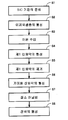
도 1은 본 발명의 실시예 1에 있어서의 SiC 반도체 장치의 제조 장치를 도시하는 모식도이다.
도 2는 본 발명의 실시예 1에 있어서의 SiC 반도체 장치의 제조 방법을 도시하는 플로우차트이다.
도 3은 본 발명의 실시예 1에 있어서의 SiC 반도체 장치의 각 제조 공정을 개략적으로 도시하는 단면도이다.
도 4는 본 발명의 실시예 1에 있어서의 SiC 반도체 장치의 각 제조 공정을 개략적으로 도시하는 단면도이다.
도 5는 본 발명의 실시예 1에 있어서의 SiC 반도체 장치의 각 제조 공정을 개략적으로 도시하는 단면도이다.
도 6은 본 발명의 실시예 1에 있어서의 SiC 반도체 장치의 각 제조 공정을 개략적으로 도시하는 단면도이다.
도 7은 본 발명의 실시예 1에 있어서의 SiC 반도체 장치의 각 제조 공정을 개략적으로 도시하는 단면도이다.
도 8은 본 발명의 실시예 1에 있어서의 SiC 반도체 장치의 각 제조 공정을 개략적으로 도시하는 단면도이다.
도 9는 본 발명의 실시예 1에 있어서의 SiC 반도체 장치의 각 제조 공정을 개략적으로 도시하는 단면도이다.
도 10은 본 발명의 실시예 1에 있어서의 SiC 반도체 장치의 각 제조 공정을 개략적으로 도시하는 단면도이다.
도 11은 본 발명의 실시예 2에 있어서의 SiC 반도체 장치의 제조 장치의 모식도이다.BRIEF DESCRIPTION OF THE DRAWINGS It is a schematic diagram which shows the manufacturing apparatus of the SiC semiconductor device in Example 1 of this invention.
FIG. 2 is a flowchart showing a method for manufacturing a SiC semiconductor device in Example 1 of the present invention. FIG.
3 is a cross-sectional view schematically showing each manufacturing step of the SiC semiconductor device in Example 1 of the present invention.
4 is a cross-sectional view schematically showing each manufacturing step of the SiC semiconductor device in Example 1 of the present invention.
5 is a cross-sectional view schematically showing each manufacturing step of the SiC semiconductor device in Example 1 of the present invention.
6 is a cross-sectional view schematically showing each manufacturing step of the SiC semiconductor device in Example 1 of the present invention.
7 is a cross-sectional view schematically showing each manufacturing step of the SiC semiconductor device in Example 1 of the present invention.
8 is a cross-sectional view schematically showing each manufacturing step of the SiC semiconductor device in Example 1 of the present invention.
9 is a cross-sectional view schematically showing each manufacturing step of the SiC semiconductor device in Example 1 of the present invention.
10 is a cross-sectional view schematically showing each manufacturing step of the SiC semiconductor device in Example 1 of the present invention.
It is a schematic diagram of the manufacturing apparatus of the SiC semiconductor device in Example 2 of this invention.
이하, 도면에 기초하여 본 발명의 실시예를 설명한다. 또한, 이하의 도면에 있어서 동일 또는 해당하는 부분에는 동일한 참조 부호를 붙이고, 그 설명은 반복하지 않는다.EMBODIMENT OF THE INVENTION Hereinafter, the Example of this invention is described based on drawing. In addition, in the following drawings, the same code | symbol is attached | subjected to the same or corresponding part, and the description is not repeated.
(실시예 1)(Example 1)
도 1은, 본 발명의 실시예 1에 있어서의 SiC 반도체 장치의 제조 장치를 도시하는 모식도이다. 도 1을 참조하여, 본 발명의 일 실시예에서의 SiC 반도체 장치의 제조 장치(10)를 설명한다.FIG. 1: is a schematic diagram which shows the manufacturing apparatus of the SiC semiconductor device in Example 1 of this invention. With reference to FIG. 1, the
도 1에 도시한 바와 같이 SiC 반도체 장치의 제조 장치(10)는, 제1 형성부(11)와, 제거부(12)와, 제2 형성부(13)와, 제1 접속부(14)와, 제2 접속부(15)를 구비하고 있다. 제거부(12)와 제2 형성부(13)는, 제1 접속부(14)에 의해 접속되어 있다. 제1 형성부(11)와 제거부(12)는, 제2 접속부(15)에 의해 접속되어 있다. 제거부(12), 제2 형성부(13) 및 제1 접속부(14)의 내부는 대기로부터 차단되어 있고, 내부는 상호 연통 가능하다. 제1 형성부(11), 제거부(12) 및 제2 접속부(15)의 내부는 대기로부터 차단되어 있고, 내부는 상호 연통 가능하다.As shown in FIG. 1, the
제1 형성부(11)는 SiC 반도체의 제1 표면에 제1 산화막을 형성한다. 제1 형성부(11)는, 예를 들면 열산화 장치, 플라즈마 발생 장치, 오존수 등의 산소를 포함하는 용액을 이용하여 제1 산화막을 형성하는 장치 등이 이용된다.The first forming
제거부(12)는 제1 형성부(11)에서 형성한 제1 산화막을 제거한다. 제거부(12)는, 예를 들면 열분해 장치, 가스를 이용한 에칭 장치, 플라즈마 발생 장치, 불화 수소(HF) 등의 용액을 이용하여 제1 산화막을 제거하는 장치 등이 이용된다.The
제1 형성부(11) 및 제거부(12)에서 이용하는 플라즈마 발생 장치는, 특별히 한정되지 않고, 예를 들면 평행 평판형 RIE(Reactive Ion Etching : 반응성 이온 에칭) 장치, ICP(Inductive Coupled Plasma : 유도 결합 플라즈마)형 RIE장치, ECR(Electron Cyclotron Resonance : 전자 사이클로트론 공명)형 RIE장치, SWP(Surface Wave Plasma : 표면파 플라즈마)형 RIE 장치 등이 이용된다.The plasma generating apparatus used in the first forming
제2 형성부(13)는, 제거부(12)에 의해, SiC 반도체에 있어서 제1 산화막이 제거됨으로써 노출된 제2 표면에, SiC 반도체 장치(도 9 참조)를 구성하는 제2 산화막을 형성한다. 제2 형성부(13)는, 예를 들면 열산화 장치, CVD(Chemical Vapor Deposition : 화학 증착) 장치 등이 이용된다.The second forming
제1 접속부(14)는, SiC 반도체를 반송 가능하게 제거부(12)와 제2 형성부(13)를 접속한다. 제2 접속부(15)는, SiC 반도체를 반송 가능하게 제1 형성부(11)와 제거부(12)를 접속한다. 제1 및 제2 접속부(14, 15)에 있어서 SiC 반도체를 반송시키는 영역(내부 공간)은 대기의 차단이 가능하다.The
여기서, 대기의 차단(대기를 차단한 분위기)이란, 대기가 혼입되지 않는 분위기를 의미하고, 예를 들면 불활성 가스나 질소 가스로 이루어지는 분위기, 진공이다. 구체적으로는, 대기를 차단한 분위기는, 예를 들면 질소(N), 헬륨(He), 네온(Ne), 아르곤(Ar), 크립톤(Kr), 크세논(Xe), 라돈(Rn), 또는 이들의 조합으로 이루어지는 가스가 충전된 분위기이다. 또한, 대기를 차단한 분위기는, 예를 들면 1 Pa 이하, 바람직하게는 0.1 Pa 이하이다.Here, the blocking of the atmosphere (atmosphere in which the atmosphere is blocked) means an atmosphere in which the atmosphere is not mixed, and is, for example, an atmosphere made of inert gas or nitrogen gas, and vacuum. Specifically, the atmosphere which cuts off the atmosphere is, for example, nitrogen (N), helium (He), neon (Ne), argon (Ar), krypton (Kr), xenon (Xe), radon (Rn), or It is an atmosphere filled with the gas which consists of these combinations. In addition, the atmosphere which cut off the atmosphere is 1 Pa or less, for example, Preferably it is 0.1 Pa or less.
본 실시예에서는, 제1 접속부(14)는 제거부(12)의 내부와 제2 형성부(13)의 내부를 연결하고 있다. 제1 접속부(14)는, 제거부(12)로부터 반출되는 SiC 반도체를 제2 형성부(13)로 반송하기 위한 공간을 내부에 갖는다. 즉, 제1 접속부(14)는 SiC 반도체를 대기에 개방하지 않도록, 제거부(12)로부터 제2 형성부(13)로 반송하기 위해서 설치되어 있다.In the present embodiment, the first connecting
마찬가지로, 제2 접속부(15)는 제1 형성부(11)의 내부와 제거부(12)의 내부를 연결하고 있다. 제2 접속부(15)는 제1 형성부(11)로부터 반출되는 SiC 반도체를 제거부(12)로 반송하기 위한 공간을 내부에 갖는다. 즉, 제2 접속부(15)는, SiC 반도체를 대기에 개방하지 않도록, 제1 형성부(11)로부터 제거부(12)로 반송하기 위해서 설치되어 있다. 또한, 제2 접속부(15)는 생략되더라도 좋다.Similarly, the second connecting
제1 및 제2 접속부(14, 15)는, 내부에서 SiC 반도체가 반송 가능한 크기를 갖는다. 또한 제1 및 제2 접속부(14, 15)는, SiC 반도체를 서셉터에 배치한 상태로 반송 가능한 크기를 갖고 있더라도 좋다. 제1 접속부(14)는, 예를 들면 제거부(12)의 출구와 제2 형성부(13)의 입구를 접속하는 로드록실이다. 제2 접속부(15)는, 예를 들면 제1 형성부(11)의 출구와, 제거부(12)의 입구를 연결하는 로드록실이다.The 1st and
또한, 제조 장치(10)는, 제1 접속부(14)의 내부에 배치되고, 제거부(12)로부터 제2 형성부(13)로 SiC 반도체를 반송하기 위한 제1 반송부를 더 구비하고 있더라도 좋다. 마찬가지로, 제조 장치(10)는, 제2 접속부(15)의 내부에 배치되고, 제1 형성부(11)로부터 제거부(12)로 SiC 반도체를 반송하기 위한 제2 반송부를 더 구비하고 있더라도 좋다. 제1 반송부와 제2 반송부는 같더라도 다르더라도 좋다.In addition, the
또한, 제조 장치(10)는 제1 및 제2 접속부(14, 15)를 덮는 단열 부재를 더 구비하고 있더라도 좋다. 또한, 제조 장치(10)는, 제1 및 제2 접속부(14, 15)의 외주에 배치되어, 제1 및 제2 접속부(14, 15)를 가열하는 가열부를 더 구비하고 있더라도 좋다. 이 경우, 제1 형성부(11), 제거부(12) 및 제2 형성부(13) 사이에서의 온도차를 저감할 수 있기 때문에, 반송으로 인한 SiC 반도체의 온도 저하를 억제할 수 있다.In addition, the
또한, 제조 장치(10)는, 제1 접속부(14) 내에 배치되고, 또한 제거부(12)의 내부와 제2 형성부(13)의 내부를 차단하기 위한 제1 차단부를 더 구비하고 있더라도 좋다. 또한 제조 장치(10)는, 제2 접속부(15) 내에 배치되고, 또한 제1 형성부(11)의 내부와 제거부(12)의 내부를 차단하기 위한 제2 차단부를 더 구비하고 있더라도 좋다. 제1 및 제2 차단부는, 예를 들면 각각의 연통부를 막는 것이 가능한 밸브나 도어 등을 이용할 수 있고, 복수로 마련되더라도 좋다.In addition, the
또한, 제조 장치(10)는, 내부의 분위기 가스를 배출하기 위한 진공 펌프나, 내부의 분위기 가스를 치환하기 위한 치환 가스봄베(가스통)를 더 구비하고 있더라도 좋다. 진공 펌프나 치환 가스봄베는, 제1 형성부(11), 제거부(12), 제2 형성부(13), 제1 접속부(14) 및 제2 접속부(15)의 각각에 접속되어 있더라도 좋고, 적어도 어느 하나에 접속되어 있더라도 좋다.In addition, the
또한, 제조 장치(10)는, 상기 이외의 여러 가지 요소를 포함하고 있더라도 좋지만, 설명의 편의상, 이들 요소의 도시 및 설명은 생략한다.In addition, although the
또한, 도 1에서는, 제1 접속부(14)는 제거부(12)와 제2 형성부(13)의 사이만을 연결하고, 제2 접속부(15)는 제1 형성부(11)와 제거부(12)의 사이만을 연결하는 형상을 나타냈지만, 특별히 이것에 한정되는 것은 아니다. 제1 및 제2 접속부(14, 15)로서, 예를 들면 대기를 차단한 챔버를 이용하고, 이 챔버 내에 제1 형성부(11), 제거부(12) 및 제2 형성부(13)가 배치되어 있더라도 좋다.In addition, in FIG. 1, the
도 2는, 본 발명의 실시예 1에서의 SiC 반도체 장치의 제조 방법을 도시하는 플로우차트이다. 도 3∼도 10은, 본 발명의 실시예 1에서의 SiC 반도체 장치의 각 제조 공정을 개략적으로 도시하는 단면도이다. 계속해서, 도 1∼도 10을 참조하여, 본 발명의 일 실시예에 있어서의 SiC 반도체 장치의 제조 방법을 설명한다. 본 실시예에서는, 도 1에 도시하는 SiC 반도체의 제조 장치(10)를 이용하여, SiC 반도체 장치의 일례로서 MOSFET(Metal Oxide Semiconductor Field Effect Transistor : 전계 효과 트랜지스터)를 제조한다.2 is a flowchart showing a method for manufacturing a SiC semiconductor device in Example 1 of the present invention. 3-10 is sectional drawing which shows roughly each manufacturing process of the SiC semiconductor device in Example 1 of this invention. Subsequently, with reference to FIGS. 1-10, the manufacturing method of the SiC semiconductor device in one Example of this invention is demonstrated. In this embodiment, a MOSFET (Metal Oxide Semiconductor Field Effect Transistor) is manufactured as an example of a SiC semiconductor device using the SiC
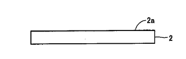
도 2 및 도 3에 도시한 바와 같이, 우선, 표면(2a)을 갖는 SiC 기판(2)을 준비한다(스텝 S1). SiC 기판(2)은, 특별히 한정되지 않지만, 예를 들면 이하의 방법에 의해 준비할 수 있다.As shown in FIG.2 and FIG.3, the
구체적으로는, 예를 들면, 승화법, CVD법, HVPE(Hydride Vapor Phase Epitaxy : 하이드라이드 기상 성장)법, MBE(Molecular Beam Epitaxy : 분자선 에피택시)법, OMVPE(Organo Metallic Vapor Phase Epitaxy : 유기 금속 기상 성장)법 등의 기상 성장법, 플럭스법, 고질소압용액법 등의 액상 성장법 등에 의해 성장된 SiC 잉곳을 준비한다. 그 후, SiC 잉곳으로부터 표면을 갖는 SiC 기판을 절출(切出)한다. 절출하는 방법은 특별히 한정되지 않고, SiC 잉곳으로부터 슬라이스 등에 의해 SiC 기판을 절출한다.Specifically, for example, the sublimation method, the CVD method, the hydride vapor phase epitaxy (HVPE) method, the molecular beam epitaxy (MBE) method, the organometallic vapor phase epitaxy (OMVPE) SiC ingots grown by a vapor phase growth method such as a vapor phase growth method, a flux method, a liquid phase growth method such as a high nitrogen pressure solution method, and the like are prepared. Thereafter, the SiC substrate having the surface is cut out from the SiC ingot. The method of cutting out is not specifically limited, A SiC substrate is cut out by a slice etc. from a SiC ingot.
계속해서, 절출한 SiC 기판의 표면을 연마한다. 연마하는 면은, 표면만이라도 좋고, 표면과 반대측의 이면을 추가로 연마하더라도 좋다. 연마하는 방법은 특별히 한정되지 않지만, 표면을 평탄하게 하고, 흠 등의 손상을 저감하기 위해서, 예를 들면 CMP(Chemical Mechanical Polishing : 화학 기계 연마)를 채용할 수 있다. CMP에서는, 연마제로서 콜로이드성의 실리카, 지립(砥粒)으로서 다이아몬드, 산화크롬, 고정제로서 접착제, 왁스 등을 이용한다. 또한, CMP와 더불어, 또는 대신해서, 전계 연마법, 화학 연마법, 기계 연마법 등의 다른 연마를 추가로 행하더라도 좋다. 또한 연마를 생략하더라도 좋다.Then, the surface of the cut SiC substrate is polished. The surface to be polished may be only the surface, or may further polish the back surface on the opposite side to the surface. Although the method of grinding | polishing is not specifically limited, In order to make a surface flat and reduce damage, such as a flaw, CMP (Chemical Mechanical Polishing) can be employ | adopted, for example. In CMP, colloidal silica is used as an abrasive, diamond, chromium oxide as an abrasive, an adhesive agent, wax, etc. are used as a fixing agent. In addition to or instead of CMP, other polishing such as an electric field polishing method, a chemical polishing method, and a mechanical polishing method may be further performed. Further, polishing may be omitted.
그 후, SiC 기판의 표면을 세정한다. 세정하는 방법은 특별히 한정되지 않지만, 예를 들면, 열산화 등에 의해 산화막을 형성한 후에, 그 산화막을 열분해, 열에칭 등에 의해 제거하는 것에 의한 세정을 채용할 수 있다. 또한 세정을 생략하더라도 좋다.Thereafter, the surface of the SiC substrate is cleaned. Although the method of washing | cleaning is not specifically limited, For example, after forming an oxide film by thermal oxidation etc., washing | cleaning by removing the oxide film by thermal decomposition, thermal etching etc. can be employ | adopted. In addition, cleaning may be omitted.
이에 따라, 도 3에 도시하는 표면(2a)을 갖는 SiC 기판(2)을 준비할 수 있다. 이러한 SiC 기판(2)으로서, 예를 들면 도전형이 n형이며, 저항이 0.02 Ω㎝인 기판을 이용한다.Thereby, the
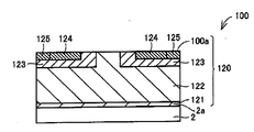
다음에, 도 2 및 도 4에 도시한 바와 같이, SiC 기판(2)의 표면(2a)상에 기상 성장법, 액상 성장법 등에 의해, 에피택셜층(120)을 형성한다(스텝 S2). 본 실시예에서는, 예를 들면 이하와 같이 에피택셜층(120)을 형성한다.Next, as shown in FIGS. 2 and 4, the
구체적으로는, 도 4에 도시한 바와 같이 SiC 기판(2)의 표면(2a) 상에, 버퍼층(121)을 형성한다. 버퍼층(121)은, 예를 들면 도전형이 n형인 SiC로 이루어지고, 예를 들면 두께가 0.5 ㎛의 에피택셜층이다. 또한 버퍼층(121)에서의 도전성 불순물의 농도는, 예를 들면 5×1017 cm-3이다.Specifically, as shown in FIG. 4, the
그 후, 도 4에 도시한 바와 같이 버퍼층(121) 상에 내압 유지층(122)을 형성한다. 내압 유지층(122)으로서, 기상 성장법, 액상 성장법 등에 의해 도전형이 n형인 SiC로 이루어지는 층을 형성한다. 내압 유지층(122)의 두께는, 예를 들면 15 ㎛이다. 또한 내압 유지층(122)에 있어서의 n형의 도전성 불순물의 농도는, 예를 들면 5×1015 cm-3이다.Thereafter, as shown in FIG. 4, the pressure
다음에, 도 2 및 도 5에 도시한 바와 같이 에피택셜층(120)에 이온 주입한다(스텝 S3). 본 실시예에서는, 도 5에 도시한 바와 같이 p형 웰 영역(123)과, n+소스 영역(124)과, p+ 컨택트 영역(125)을 이하와 같이 형성한다. 우선 도전형이 p형인 불순물을 내압 유지층(122)의 일부에 선택적으로 주입하는 것으로, 웰 영역(123)을 형성한다. 그 후, n형의 도전성 불순물을 소정의 영역에 선택적으로 주입함으로써 소스 영역(124)을 형성하고, 또한 도전형이 p형인 도전성 불순물을 소정의 영역에 선택적으로 주입함으로써 컨택트 영역(125)을 형성한다. 또 불순물의 선택적인 주입은, 예를 들면 산화막으로 이루어지는 마스크를 이용하여 행해진다. 이 마스크는, 불순물의 주입 후에 각각 제거된다.Next, as shown in FIGS. 2 and 5, ion implantation into the
이와 같이 이온 주입하는 스텝 S3 후에, 활성화 어닐링 처리가 행하여지더라도 좋다. 예를 들면, 아르곤 분위기 중, 가열 온도 1700℃로 30분간의 어닐링이 행해진다.Thus, after step S3 of ion implantation, an activation annealing process may be performed. For example, annealing for 30 minutes is performed at 1700 degreeC of heating temperature in argon atmosphere.
또한 이온 주입하는 스텝 S3 후에, 유기 세정, 산세정, RCA 세정 등의 표면 세정화를 추가로 행하더라도 좋다.In addition, after step S3 of ion implantation, surface cleaning such as organic cleaning, pickling, RCA cleaning, or the like may be further performed.
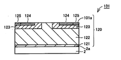
이들 공정에 의해, 도 5에 도시한 바와 같이 SiC 기판(2)과, SiC 기판(2) 상에 형성된 에피택셜층(120)을 구비한 에피택셜 웨이퍼(100)를 준비할 수 있다.By these processes, the
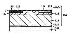
다음에, 에피택셜 웨이퍼(100)(SiC 반도체)의 표면(100a)(제1 표면)을 세정한다. 구체적으로는, 도 2 및 도 6에 도시한 바와 같이, 에피택셜 웨이퍼(100)의 표면(100a)에 제1 산화막(3)을 형성한다(스텝 S4). 제1 산화막(3)은, 예를 들면 산화 실리콘이다. 본 실시예의 스텝 S4에서는, 도 1에 도시하는 제조 장치(10)의 제1 형성부(11)에서 제1 산화막(3)을 형성한다.Next, the
제1 산화막(3)의 형성 방법은, 특별히 한정되지 않고, 예를 들면 O를 포함하는 용액, O 플라즈마, O 가스를 포함하는 분위기에서의 열산화 등을 이용하여, 에피택셜 웨이퍼(100)의 표면(100a)을 산화하는 방법이 이용된다.The formation method of the
O를 포함하는 용액이란, 산소를 포함하는 용액을 의미하며, 예를 들면 오존수를 들 수 있다. SiC가 안정된 화합물인 것을 고려하면, 예를 들면 30 ppm 이상의 농도를 갖는 오존수를 이용하는 것이 바람직하다. 이 경우, 오존의 분해를 억제할 수 있고, 에피택셜 웨이퍼(100)의 표면(100a)과 오존과의 반응 속도를 높일 수 있기 때문에, 표면(100a)에 제1 산화막(3)을 용이하게 형성할 수 있다.The solution containing O means the solution containing oxygen, and ozone water is mentioned, for example. Considering that SiC is a stable compound, it is preferable to use ozone water having a concentration of 30 ppm or more, for example. In this case, since decomposition of ozone can be suppressed and the reaction rate between the
또한, O 가스란 산소를 포함하는 가스를 의미하며, O 가스를 포함하는 열산화는, SiC가 안정된 화합물인 것을 고려하면, 예를 들면 700℃ 이상 온도의 드라이 분위기에서 행하는 것이 바람직하다. 또한, 드라이 분위기란 기상 중에서 제1 산화막(3)을 형성하는 것을 의미하며, 의도하지 않는 액상 성분을 포함하고 있더라도 좋다.In addition, O gas means the gas containing oxygen, and considering that thermal oxidation containing O gas is a compound which SiC is stable, it is preferable to carry out in dry atmosphere of temperature 700 degreeC or more, for example. In addition, a dry atmosphere means forming the
또한, O 플라즈마란 산소를 포함하는 가스로부터 생성되는 플라즈마를 의미하고, 예를 들면 산소 가스(O2)를 플라즈마 발생 장치에 공급함으로써 발생시킬 수 있다. 「O 플라즈마에 의해 제1 산화막(3)을 형성한다」라는 것은, 산소를 포함하는 가스를 이용한 플라즈마에 의해 제1 산화막(3)을 형성하는 것을 의미한다. 다시 말해서, 산소를 포함하는 가스로부터 생성되는 플라즈마에 의해서 처리됨으로써, 제1 산화막(3)을 형성하는 것을 의미한다.In addition, plasma is O can sense a plasma generated from a gas containing oxygen, and, for example, generated by supplying an oxygen gas (O 2) in the plasma generating device. "Forming the
이 스텝 S4에 있어서, 표면(100a)에 부착된 불순물, 파티클을 제거하는 것을 목적으로 하는 경우에는, 예를 들면 1분자층 이상 10 ㎚ 이하의 두께[표면(100a)에서 SiC 기판(2)을 향한 방향의 두께]의 제1 산화막(3)을 형성한다. 1분자층 이상의 두께를 갖는 제1 산화막(3)을 형성하는 것으로, 표면(100a)에 부착해 있는 불순물, 파티클 등을 제1 산화막(3)의 표면이나 내부에 받아들일 수 있다. 10 ㎚ 이하 두께의 산화막을 형성하는 것으로, 후술하는 스텝 S5에서 제1 산화막(3)은 쉽게 제거된다. 표면(100a)의 불순물, 파티클을 받아들여 산화하는 경우에는, 액상에 의한 세정(웨트 세정) 및 기상에 의한 세정(드라이 세정)을 이용할 수 있다.In this step S4, when it is aimed at removing the impurities and particles adhering to the
에피택셜 웨이퍼(100)에 이온 주입이나 활성화 어닐링 처리 등에 의해 표면(100a)이 손상을 받아, 에피택셜 웨이퍼(100)의 표면(100a)에 형성된 손상층을 제거하는 것을 목적으로 하는 경우에는, 이 스텝 S4에 있어서 손상층을 산화한다. 이 경우, 예를 들면 10 ㎚ 초과 100 ㎚ 이하의 두께를 갖는 제1 산화막(3)을 형성한다. 손상층을 산화함으로써, 표면(100a)에 부착된 불순물, 파티클 등을 제1 산화막(3)에 받아들일 수도 있다. 손상층을 산화하는 경우에는, 기상에 의한 세정(드라이 세정)을 채용한다. 여기서, 손상층은 다른 영역에 비교해서 표면 거침 등이 생기기 때문에, 예를 들면 SIMS 분석을 행함으로써, 비주입 영역에 비교해서 지나치게 규소 또는 탄소(C)가 존재하고 있는 것에 의해 특정된다.In the case where the
다음에, 도 1을 참조하여, 제1 형성부(11)에서 제1 산화막(3)을 형성한 에피택셜 웨이퍼(100)를, 제거부(12)로 반송한다. 이때, 에피택셜 웨이퍼(100)는 대기가 차단된 분위기인 제2 접속부(15) 내에서 반송된다. 다시 말해서, 제1 산화막(3)을 형성하는 스텝 S4와 제1 산화막(3)을 제거하는 스텝 S5 사이에서는, 에피택셜 웨이퍼(100)는 대기가 차단된 분위기 내에 배치된다. 이에 따라, 제1 산화막(3)이 형성된 후에, 에피택셜 웨이퍼(100)의 표면(101a)에 대기중에 포함되는 불순물이 부착하는 것을 억제할 수 있다.Next, with reference to FIG. 1, the
다음에, 도 2 및 도 7에 도시한 바와 같이, 제1 산화막(3)을 제거한다(스텝 S5). 본 실시예의 스텝 S5에서는, 도 1에 도시하는 제조 장치(10)의 제거부(12)에서 제1 산화막(3)을 제거한다.Next, as shown in FIG. 2 and FIG. 7, the
제1 산화막(3)의 제거 방법은, 특별히 한정되지 않고, 예를 들면 웨트 에칭, 드라이 에칭, 열 분해, F 플라즈마 등을 이용할 수 있다.The removal method of the
웨트 에칭은, 예를 들면 HF, NH4F(불화 암모늄) 등의 용액을 이용하여 제1 산화막(3)을 제거한다.Wet etching, for example, to remove the
드라이 에칭은, 800℃ 이상 SiC의 승화 온도 이하, 바람직하게는 1000℃ 이상 SiC의 승화 온도 이하에서, 수소 가스, 염화 수소 가스, 불화유황 가스 및 불화탄소 가스로 이루어지는 군으로부터 선택되는 적어도 하나를 포함하는 가스를 이용하여, 제1 산화막(3)을 제거하는 것이 바람직하다. 800℃ 이상의 수소 가스, 염화 수소 가스, 불화유황 가스 및 불화탄소 가스는 제1 산화막(3)을 환원하는 효과가 높다. 이러한 관점에서 1000℃ 이상이 보다 바람직하다. 제1 산화막이 SiOx인 경우, 수소 가스는 SiOx를 H2O와 SiHy로 분해하고, 염화 수소 가스는 SiOx를 H2O와 SiClz로 분해한다. SiC의 승화 온도 이하로 함으로써 에피택셜 웨이퍼(100)의 열화를 억제할 수 있다. 또한, 드라이 에칭은 반응을 촉진할 수 있는 관점에서, 감압하에서 행하는 것이 바람직하다.The dry etching includes at least one selected from the group consisting of hydrogen gas, hydrogen chloride gas, sulfur fluoride gas, and carbon fluoride gas at a sublimation temperature of SiC of at least 800 ° C or less, preferably of at least 1000 ° C or less of SiC. It is preferable to remove the
열분해는 산소를 포함하지 않는 분위기에서 1200℃ 이상 SiC의 승화 온도 이하에서, 제1 산화막(3)을 열분해하는 것이 바람직하다. 1200℃ 이상의 산소를 포함하지 않는 분위기에서 에피택셜 웨이퍼(100)의 표면(100a)에 형성된 제1 산화막(3)을 가열하면 제1 산화막(3)을 용이하게 열분해할 수 있다. SiC의 승화 온도 이하로 함으로써 에피택셜 웨이퍼(100)의 열화를 억제할 수 있다. 또한, 열분해는 반응을 촉진할 수 있는 관점에서, 감압하에서 행하는 것이 바람직하다.Pyrolysis is preferably pyrolyzing the
F 플라즈마란, 불소(F)를 포함하는 가스로부터 생성되는 플라즈마를 의미하며, 예를 들면 사불화 탄소 가스(CF4), 삼불화 메탄 가스(CHF3), 육불화 에탄 가스(C2F6), 육불화 유황 가스(SF6), 삼불화 질소 가스(NF3), 이불화 크세논 가스(XeF2), 불소 가스(F2) 및 삼불화 염소 가스(ClF3)의 단독 가스 또는 혼합 가스를 플라즈마 발생 장치에 공급함으로써 발생시킬 수 있다. 「F 플라즈마에 의해 제1 산화막(3)을 제거한다」라는 것은, 불소를 포함하는 가스를 이용한 플라즈마에 의해 제1 산화막(3)을 제거하는 것을 의미한다. 다시 말해서, 불소를 포함하는 가스로부터 생성되는 플라즈마에 의해서 처리됨으로써, 제1 산화막(3)을 제거하는 것을 의미한다.The F plasma means a plasma generated from a gas containing fluorine (F), and for example, carbon tetrafluoride gas (CF 4 ), methane trifluoride gas (CHF 3 ), and ethane hexafluoride gas (C 2 F 6). ), Single or mixed gas of sulfur hexafluoride gas (SF 6 ), nitrogen trifluoride gas (NF 3 ), xenon difluoride (XeF 2 ), fluorine gas (F 2 ) and chlorine trifluoride gas (ClF 3 ) Can be generated by supplying the plasma generator. "Removing the
이 스텝 S5를 실시함으로써, 스텝 S4에서 불순물, 파티클 등을 받아들인 제1 산화막(3)을 제거하기 때문에, 에피택셜 웨이퍼(100) 표면(100a)의 불순물, 파티클 등을 제거할 수 있다. 이에 따라, 도 7에 도시한 바와 같이, 불순물, 파티클 등이 저감된 표면(101a)(제2 표면)을 갖는 에피택셜 웨이퍼(101)를 형성할 수 있다.By performing this step S5, the
또한, 스텝 S4에서 손상층을 산화시킨 제1 산화막(3)을 형성한 경우에는, 스텝 S5를 실시함으로써, 손상층도 추가로 제거할 수 있다. 이에 따라, 도 7에 도시한 바와 같이, 불순물, 파티클 등이 저감된 표면(101a)을 갖는 에피택셜 웨이퍼(101)를 형성할 수 있다. 이에 따라, 도 7에 도시한 바와 같이, 불순물, 파티클 등이 저감되고, 또한 손상층이 제거된 표면(101a)을 갖는 에피택셜 웨이퍼(101)를 형성할 수 있다.In addition, when the
또한, 상기 스텝 S4 및 S5를 반복하더라도 좋다. 또한 필요에 따라, 다른 물약으로의 세정 공정, 순수한 물 린스 공정, 건조 공정 등을 추가하여 실시하더라도 좋다. 다른 물약은, 예를 들면 황산과 과산화수소수를 포함하는 SPM을 들 수 있다. 스텝 S2 전에 SPM으로 세정하는 경우에는 유기물을 제거할 수도 있다. 단, 제1 산화막(3)을 제거하는 스텝 S5와, 후술하는 게이트 산화막(126)을 형성하는 스텝 S6 사이에 다른 공정이 추가되는 경우에는, 다른 공정으로의 이행시에 있어서도 에피택셜 웨이퍼는 대기가 차단된 분위기 내에 배치된다.In addition, you may repeat said step S4 and S5. Moreover, you may add and perform a washing process with another potion, a pure water rinse process, a drying process, etc. as needed. Another potion is, for example, SPM containing sulfuric acid and hydrogen peroxide water. In the case of washing with SPM before step S2, the organic matter may be removed. However, if another step is added between step S5 for removing the
다음에, 도 1을 참조하여, 제거부(12)에서 제1 산화막(3)을 제거한 에피택셜 웨이퍼(101)를, 제2 형성부(13)로 반송한다. 이때, 에피택셜 웨이퍼(101)는 대기가 차단된 분위기인 제1 접속부(14) 내에서 반송된다. 다시 말해서, 제1 산화막(3)을 제거하는 스텝 S5와 제2 산화막으로서의 게이트 산화막을 형성하는 스텝 S6 사이에서는, 에피택셜 웨이퍼(101)는 대기가 차단된 분위기 내에 배치된다. 이에 따라, 제1 산화막(3)이 제거된 후에, 에피택셜 웨이퍼(101)의 표면(101a)에 대기중에 포함되는 불순물이 부착하는 것을 억제할 수 있다.Next, referring to FIG. 1, the
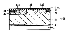
다음에, 도 2 및 도 8에 도시한 바와 같이, 에피택셜 웨이퍼(101)에 있어서 제1 산화막(3)이 제거됨으로써 노출된 표면(101a)(제2 표면)에, SiC 반도체 장치를 구성하는 제2 산화막으로서의 게이트 산화막(126)을 형성한다(스텝 S6). 구체적으로는, 도 8에 도시한 바와 같이 내압 유지층(122)과, 웰 영역(123)과, 소스 영역(124)과, 컨택트 영역(125)의 위를 덮도록, 게이트 산화막(126)을 형성한다. 이 형성은 예를 들면 열산화(드라이 산화)에 의해 행할 수 있다. 열산화는, 예를 들면 O2, O3, N2O 등의 산소를 포함하는 분위기 속에서 고온으로 가열한다. 열산화의 조건은, 예를 들면, 가열 온도가 1200℃이며, 또한 가열 시간이 30분이다. 또한, 게이트 산화막(126)의 형성은, 열산화에 한정되지 않고, 예를 들면 CVD법, 스퍼터링법 등에 의해 형성하더라도 좋다. 게이트 산화막(126)은, 예를 들면 50 ㎚의 두께를 갖는 실리콘 산화막으로 이루어진다.Next, as shown in FIGS. 2 and 8, the SiC semiconductor device is formed on the
제1 산화막(3)을 제거하는 스텝 S5와, 게이트 산화막(126)을 형성하는 스텝 S6 사이에서, 세정된 표면(101a)을 갖는 에피택셜 웨이퍼(101)의 온도차를 500℃ 이하로 유지하는 것이 바람직하다. 이 경우, 스텝 S5와 스텝 S6 사이에서의 에피택셜 웨이퍼의 온도차가 작기 때문에, 작업 처리량을 향상시킬 수 있다. 제1 산화막(3)을 형성하는 스텝 S4와, 제1 산화막(3)을 제거하는 스텝 S5와, 게이트 산화막(126)을 형성하는 스텝 S6의 각각의 사이에 있어서, 에피택셜 웨이퍼(100, 101)의 온도차를 500℃ 이하로 유지하는 것이 보다 바람직하다. 이 경우, 스텝 S4 개시로부터 스텝 S6 종료까지의 사이에 있어서, 에피택셜 웨이퍼의 온도차가 작기 때문에, 작업 처리량을 향상시킬 수 있다.Maintaining the temperature difference of the
또한, 제1 산화막(3)을 제거하는 스텝 S5와, 게이트 산화막(126)을 형성하는 스텝 S6 사이에 있어서, 세정된 표면(101a)을 갖는 에피택셜 웨이퍼(101)를 800℃ 이상으로 유지하는 것이 바람직하고, 1000℃ 이상으로 유지하는 것이 보다 바람직하다. 이 경우, 스텝 S5와 스텝 S6 사이에서의 에피택셜 웨이퍼의 온도 저하를 억제할 수 있기 때문에, 작업 처리량을 향상시킬 수 있다. 또한, 제1 산화막(3)을 형성하는 스텝 S4와, 제1 산화막(3)을 제거하는 스텝 S5와, 게이트 산화막(126)을 형성하는 스텝 S6의 각각의 사이에 있어서, 에피택셜 웨이퍼(100, 101)를 800℃ 이상으로 유지하는 것이 바람직하고, 1000℃ 이상으로 유지하는 것이 보다 바람직하다. 이 경우, 스텝 S4 개시로부터 스텝 S6 종료까지의 사이에 있어서, 에피택셜 웨이퍼의 온도의 저하를 억제할 수 있기 때문에, 작업 처리량을 향상시킬 수 있다.In addition, between step S5 of removing the
그 후, 질소 어닐링을 행한다(스텝 S7). 구체적으로는, 일산화질소(NO) 분위기 중에서의 어닐링 처리가 행하여진다. 이 처리의 조건은, 예를 들면 가열 온도가 1100℃이며, 가열 시간이 120분이다. 그 결과, 내압 유지층(122), 웰 영역(123), 소스 영역(124) 및 컨택트 영역(125)의 각각과, 게이트 산화막(126)의 계면 근방에, 질소 원자를 도입할 수 있다.Thereafter, nitrogen annealing is performed (step S7). Specifically, an annealing treatment in a nitrogen monoxide (NO) atmosphere is performed. As for the conditions of this process, a heating temperature is 1100 degreeC, for example, and a heat time is 120 minutes. As a result, nitrogen atoms can be introduced into each of the breakdown
또한, 이 일산화질소를 이용한 어닐링 공정 후, 추가로 불활성 가스인 아르곤 가스를 이용한 어닐링 처리를 하더라도 좋다. 이 처리의 조건은, 예를 들면, 가열 온도가 1100℃이며, 가열 시간이 60분이다.After the annealing step using nitrogen monoxide, annealing treatment using argon gas, which is an inert gas, may be further performed. As for the conditions of this process, a heating temperature is 1100 degreeC and a heating time is 60 minutes, for example.
이 질소 어닐링 공정(스텝 S7) 후, 유기 세정, 산세정, RCA 세정 등의 표면 세정화를 추가로 하더라도 좋다.After this nitrogen annealing step (step S7), surface cleaning such as organic cleaning, pickling, and RCA cleaning may be further performed.
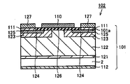
다음에, 도 2, 도 9 및 도 10에 도시한 바와 같이, 전극을 형성한다(스텝 S8). 우선, 도 9에 도시하는 소스 전극(111)을, 이하와 같이 형성한다. 구체적으로는, 게이트 산화막(126) 상에 포토리소그래피법을 이용하여, 패턴을 갖는 레지스트막을 형성한다. 이 레지스트막을 마스크로서 이용하여, 게이트 산화막(126) 중 소스 영역(124) 및 컨택트 영역(125) 상에 위치하는 부분을 에칭에 의해 제거한다. 이에 따라 게이트 산화막(126)에 개구부(126a)를 형성한다. 예를 들면 증착법에 의해, 이 개구부(126a)에서 소스 영역(124) 및 컨택트 영역(125)의 각각과 접촉하도록 도전체막을 형성한다. 다음에 레지스트막을 제거함으로써, 상기 도체막 중 레지스트막 상에 위치해 있었던 부분의 제거(리프트 오프)가 행하여진다. 이 도체막은, 금속막이라도 좋고, 예를 들면 니켈(Ni)로 이루어진다. 이 리프트 오프의 결과, 소스 전극(111)이 형성된다.Next, as shown in FIG. 2, FIG. 9, and FIG. 10, an electrode is formed (step S8). First, the
또한, 여기서 얼로이화를 위한 열처리가 행해지는 것이 바람직하다. 예를 들면, 불활성 가스인 아르곤(Ar) 가스의 분위기 속에서, 가열 온도 950℃로 2분의 열처리가 행해진다.In addition, it is preferable that heat processing for alloying is performed here. For example, heat treatment for 2 minutes is performed at the heating temperature of 950 degreeC in the atmosphere of argon (Ar) gas which is an inert gas.
그 후, 도 10에 도시한 바와 같이, 예를 들면 증착법에 의해 소스 전극(111) 상에 상부 소스 전극(127)을 형성한다. 또한, 예를 들면 증착법에 의해, SiC 기판(2)의 이면 상에 드레인 전극(112)을 형성한다.Then, as shown in FIG. 10, the
또한 게이트 전극(110)을 예를 들면 이하와 같이 형성한다. 미리 게이트 산화막(126) 상의 영역에 위치하는 개구 패턴을 갖는 레지스트막을 형성하고, 해당 레지스트막의 전체 면을 덮도록 게이트 전극을 구성하는 도전체막을 형성한다. 그리고, 레지스트막을 제거함으로써, 게이트 전극이 되어야 하는 도전체막의 부분 이외의 도전체막을 제거(리프트 오프)한다. 그 결과, 도 10에 도시한 바와 같이, 게이트 산화막(126) 상에 게이트 전극(110)을 형성할 수 있다.In addition, the
이상의 공정(스텝 S1∼S8)을 실시함으로써, 도 10에 도시하는 SiC 반도체 장치로서의 MOSFET(102)를 제조할 수 있다.By performing the above steps (steps S1 to S8), the
또한, 본 실시예에 있어서의 도전형이 교체된 구성, 즉 p형과 n형이 교체된 구성을 이용할 수도 있다.In addition, a configuration in which the conductive type is replaced in this embodiment, that is, a configuration in which the p-type and n-type are replaced may be used.
또한, MOSFET(102)를 제작하기 위해서 SiC 기판(2)을 이용하고 있지만, 기판의 재료는 SiC에 한정되지 않고, 다른 재료의 결정을 이용하여 제작되더라도 좋다. 또한, SiC 기판(2)이 생략되더라도 좋다.In addition, although the
이상 설명한 바와 같이, 본 실시예에 있어서의 SiC 반도체 장치의 일례로서의 MOSFET(102)의 제조 방법은, 제1 산화막(3)을 제거하는 스텝 S5와, 제2 산화막으로서의 MOSFET(102)를 구성하는 게이트 산화막(126)을 형성하는 스텝 S6의 사이에 있어서, SiC 반도체로서의 에피택셜 웨이퍼(101)는 대기가 차단된 분위기 내에 배치된다.As described above, the method of manufacturing the
본 실시예에 있어서의 SiC 반도체 장치의 일례로서의 MOSFET(102)의 제조 장치(10)는, 에피택셜 웨이퍼(101)를 반송 가능하게 제거부(12)와 제2 형성부(13)를 접속하는 제1 접속부(14)를 구비하고, 제1 접속부(14)에 있어서의 에피택셜 웨이퍼(101)를 반송시키는 영역은 대기의 차단이 가능하다.The
본 발명 MOSFET(102)의 제조 방법 및 제조 장치에 따르면, 제1 산화막을 형성하는 스텝 S4에 있어서, 에피택셜 웨이퍼(100)의 표면(100a)에 부착해 있었던 티탄(Ti) 등의 불순물, 파티클 등을 제1 산화막(3)에 받아들일 수 있다. 제1 산화막(3)을 제거하는 스텝 S5에 의해, 에피택셜 웨이퍼(100)의 표면(100a)에 부착해 있었던 불순물, 파티클 등을 제거할 수 있다. 불순물, 파티클 등이 제거된 표면(101a)을 갖는 에피택셜 웨이퍼(101)를 대기가 차단된 분위기 내(제1 접속부(14))에 배치하는 것으로, 대기중의 불순물, 파티클 등이 세정후의 에피택셜 웨이퍼(101)의 표면(101a)에 재부착하는 것을 억제할 수 있기 때문에, 게이트 산화막(126) 형성 전의 에피택셜 웨이퍼(101)의 표면(101a)을 청정하게 유지할 수 있다. 게이트 산화막(126)을 형성하는 스텝 S6에 있어서, 이 상태의 에피택셜 웨이퍼(101)의 표면(101a)에, SiC 반도체 장치를 구성하는 게이트 산화막(126)을 형성할 수 있기 때문에, 에피택셜 웨이퍼(101)와 게이트 산화막(126)의 계면에 존재하는 불순물, 파티클 등을 저감할 수 있다. 또한, 에피택셜 웨이퍼(101)의 표면(101a)을 청정하게 유지할 수 있기 때문에, 표면(101a) 상에 형성하는 게이트 산화막(126) 중에 존재하는 불순물, 파티클 등도 저감할 수 있다. 또한, 게이트 산화막(126)의 막질도 향상시킬 수 있다. 따라서, MOSFET(102)의 역방향 전압 인가시의 내압을 향상시킬 수 있고, 순방향 전압 인가시의 동작의 안정성 및 장기간 신뢰성을 향상시킬 수 있다. 따라서, 특성을 향상시킬 수 있는 MOSFET(102)를 제조할 수 있다.According to the manufacturing method and manufacturing apparatus of the
본 실시예에서는, 에피택셜 웨이퍼(100)의 표면에 제1 산화막(3)을 형성하고, 제1 산화막(3)을 제거함으로써 표면을 세정한 후에, 에피택셜 웨이퍼(101)가 대기에 노출되는 것에 기인한 재오염의 가능성을 저감하고 있다. SiC는 안정된 화합물이기 때문에, 에피택셜 웨이퍼(100)의 표면(100a)에 제1 산화막(3)을 형성하는 것은 Si와 비교해서 용이하지 않다. 이 때문에, SiC 반도체인 에피택셜 웨이퍼(100)의 표면(100a)을 세정한 후에, 에피택셜 웨이퍼(101)를 대기에 노출시키지 않고서 다음 스텝(게이트 산화막을 형성하는 스텝 S6)으로 반송하는 것은, 세정을 간략화할 수 있고, 제조하는 SiC 반도체 장치의 특성 향상에 크게 기여한다.In the present embodiment, after the
또한, 대기가 차단된 분위기의 제1 접속부(14) 내에 에피택셜 웨이퍼(101)를 배치하는 것에 의해, 제1 산화막(3)을 제거하는 제거부(12)와 제2 형성부(13) 사이에서 파티클, 불순물 등의 오염 물질이 서로 묻어 들어가기 어렵게 된다. 마찬가지로, 제1 산화막(3)을 제거하는 스텝 S5 및 게이트 산화막(126)을 형성하는 스텝 S6의 각 스텝 사이에서의 오염물이 묻어 들어갈 가능성을 저감할 수 있다. 따라서, 제거부(12) 및 제2 형성부(13)의 청정화를 유지할 수 있기 때문에, 제조하는 SiC 반도체 장치의 특성의 향상에 크게 기여한다.In addition, the
본 실시예에서의 SiC 반도체 장치의 일례인 MOSFET(102)의 제조 방법에 있어서 바람직하게는, 제1 산화막(3)을 형성하는 스텝 S4와, 제1 산화막(3)을 제거하는 스텝 S5와, 게이트 산화막(126)을 형성하는 스텝 S6 사이에 있어서, 에피택셜 웨이퍼(100, 101)는 대기가 차단된 분위기 내에 배치된다.In the method of manufacturing the
본 실시예에서의 SiC 반도체 장치의 일례인 MOSFET(102)의 제조 장치(10)에 있어서 바람직하게는, 에피택셜 웨이퍼(100)를 반송 가능하게 제1 형성부(11)와 제거부(12)를 접속하는 제2 접속부(15)를 더 구비하고, 제2 접속부(15)에 있어서의 에피택셜 웨이퍼(101)를 반송시키는 영역은 대기의 차단이 가능하다.In the
이에 따라, 세정 공정 개시로부터 종료까지 에피택셜 웨이퍼가 대기에 노출되는 것을 억제할 수 있고, 또한 세정 공정 종료에서 게이트 산화막 형성까지 에피택셜 웨이퍼(101)가 대기에 노출되는 것을 억제할 수 있다. 따라서, 세정 중과 세정 후의 에피택셜 웨이퍼(100, 101)의 표면(100a, 101a)이 재오염되는 것을 억제할 수 있기 때문에, 특성을 더 향상시킬 수 있는 SiC 반도체 장치를 제조할 수 있다.As a result, the exposure of the epitaxial wafer to the atmosphere from the start of the cleaning process to the end can be suppressed, and the exposure of the
또한, 본 실시예에서는, SiC 반도체 장치로서 MOSFET의 제조 방법을 예를 들어 설명했지만, 본 발명은 표면을 갖는 SiC 에피택셜 웨이퍼와, 이 표면에 형성되는 SiC 반도체 장치를 구성하는 산화막(SiC 반도체 장치로서 남는 산화막)을 구비한 반도체 장치에 적용할 수 있다. SiC 에피택셜 웨이퍼는, 표면에 이온 주입된 것과, 이온 주입되어 있지 않은 것을 포함한다. 즉, 본 발명은 예를 들면 MOSFET이나 IGBT(Insulated Gate Bipolar Transistor : 절연 게이트 바이폴라 트랜지스터) 등의 절연 게이트형 전계 효과부를 갖는 반도체 장치나, JFET(Junction Field-Effect Transistor : 접합 전계 효과 트랜지스터) 등의 산화막을 갖춘 SiC 반도체 장치 전반에 적용할 수 있다.In the present embodiment, a method of manufacturing a MOSFET is described as an SiC semiconductor device by way of example. However, the present invention provides an SiC epitaxial wafer having a surface and an oxide film (SiC semiconductor device) constituting a SiC semiconductor device formed on this surface. It can be applied to a semiconductor device having an oxide film remaining as a layer. SiC epitaxial wafers include those implanted on the surface and those not implanted. That is, the present invention is, for example, a semiconductor device having an insulated gate field effect unit such as a MOSFET or an Insulated Gate Bipolar Transistor (IGBT), or a Junction Field-Effect Transistor (JFET). It is applicable to the whole SiC semiconductor device provided with an oxide film.
(실시예 2)(Example 2)
도 11은 본 발명의 실시예 2에 있어서의 SiC 반도체 장치의 제조 장치의 모식도이다. 도 11 등을 참조하여, 본 실시예 2에 있어서의 SiC 반도체 장치의 제조 장치를 설명한다.It is a schematic diagram of the manufacturing apparatus of the SiC semiconductor device in Example 2 of this invention. With reference to FIG. 11 etc., the manufacturing apparatus of the SiC semiconductor device in Example 2 is demonstrated.
도 11에 도시한 바와 같이, 본 실시예의 제조 장치(20)는, 챔버(21)와, 제1 가스 공급부(22)와, 제2 가스 공급부(23)와, 진공 펌프(24)를 구비하고 있다. 제1 가스 공급부(22), 제2 가스 공급부(23) 및 진공 펌프(24)는 챔버(21)와 접속되어 있다.As shown in FIG. 11, the
챔버(21)는 내부에 에피택셜 웨이퍼(100, 101)(도 5∼도 7 참조)를 수용한다. 챔버(21)는, 예를 들면 플라즈마 발생 장치를 이용할 수 있다.The
제1 가스 공급부(22)는, 에피택셜 웨이퍼(100)에 제1 산화막(3)(도 6 참조)을 형성하기 위해, 그리고 SiC 반도체 장치[본 실시예에서는 MOSFET(102)]를 구성하는 산화막[본 실시예에서는 게이트 산화막(126)]을 형성하기(도 8 참조) 위해, 이용되는 가스를 챔버(21)에 공급한다. 제1 가스 공급부(22)는, 예를 들면 산소를 포함하는 가스를 공급한다.The first
제2 가스 공급부(23)는, 에피택셜 웨이퍼(100)에 형성한 제1 산화막(3)을 제거하기 위해서 이용되는 가스를 챔버(21)에 공급한다. 제2 가스 공급부(23)는, 예를 들면 H2 가스, HCl 가스 등의 규소(Si)와 산소를 환원하는 가스를 챔버(21)에 공급한다.The second
진공 펌프(24)는, 챔버(21)의 내부를 진공으로 한다. 이 때문에, 제1 가스 공급부(22)에 의해 에피택셜 웨이퍼(100)에 제1 산화막(3)을 형성한 후에, 챔버(21)의 내부를 진공으로 하고, 제2 가스 공급부(23)에 의해 제1 산화막(3)을 제거할 수 있다. 또한, 제1 산화막(3)을 제거한 후에, 챔버(21)의 내부를 진공으로 하고, 제1 가스 공급부(22)에 의해 SiC 반도체 장치를 구성하는 제2 산화막[게이트 산화막(126)]을 에피택셜 웨이퍼(101)에 형성할 수 있다. 또한, 진공 펌프(24)는 생략되더라도 좋다.The
또한, 도 11에 도시하는 제조 장치(20)는 상기 이외의 여러 가지 요소를 포함하고 있더라도 좋지만, 설명의 편의상, 이들 요소의 도시 및 설명은 생략한다.In addition, although the
본 실시예에 있어서의 SiC 반도체 장치의 제조 방법은, 도 9에 도시하는 MOSFET(102)를 제조하고, 기본적으로는 실시예 1과 마찬가지이지만, 도 11에 도시하는 제조 장치(20)를 이용하는 점에서 다르다. 이 때문에, 제1 산화막을 형성하는 스텝 S4와 제1 산화막을 제거하는 스텝 S5의 사이, 및 제1 산화막을 제거하는 스텝 S5와 게이트 산화막(126)을 형성하는 스텝 S6의 사이에 있어서, 에피택셜 웨이퍼는 챔버(21) 내에 배치되기 때문에, 대기가 차단된 분위기 내에 배치된다.The manufacturing method of the SiC semiconductor device in this embodiment manufactures the
또한, 제1 산화막(3)을 제거하는 스텝 S5에서 이용하는 장치를 이용하여 제2 산화막으로서의 게이트 산화막(126)을 형성할 수 있다. 다시 말해서, 제1 산화막(3)을 제거하는 스텝 S5와 게이트 산화막(126)을 형성하는 스텝 S6은 동일한 장치로 실시된다. 이 때문에, 제1 산화막을 제거하는 스텝 S5와 게이트 산화막을 형성하는 스텝 S6의 사이에 있어서, 에피택셜 웨이퍼의 온도를 가능한 한 내려가지 않도록(예를 들면 500℃ 이하로) 유지할 수도 있다. 또한, 제1 산화막을 제거하는 스텝 S5와 게이트 산화막을 형성하는 스텝 S6의 사이에 있어서, 에피택셜 웨이퍼의 온도를 800℃ 이상으로, 바람직하게는 1000℃ 이상으로 유지할 수도 있다.Further, the
또한, 본 실시예에서는, 제1 산화막(3)을 형성하는 스텝 S4와, 제1 산화막(3)을 제거하는 스텝 S5와, 게이트 산화막(126)을 형성하는 스텝 S6은, 동일한 장치로 실시된다. 이 때문에, 제1 산화막(3)을 형성하는 스텝 S4와 제1 산화막(3)을 제거하는 스텝 S5의 사이, 및 제1 산화막(3)을 제거하는 스텝 S5와 게이트 산화막(126)을 형성하는 스텝 S6의 사이에 있어서, 에피택셜 웨이퍼의 온도를 가능한 한 내려가지 않도록(예를 들면 500℃ 이하로) 유지할 수도 있다. 또한, 제1 산화막을 형성하는 스텝 S4와 제1 산화막을 제거하는 스텝 S5의 사이, 및 제1 산화막을 제거하는 스텝 S5와 게이트 산화막을 형성하는 스텝 S6의 사이에 있어서, 에피택셜 웨이퍼의 온도를 800℃ 이상, 바람직하게는 1000℃ 이상으로 유지할 수도 있다.In the present embodiment, step S4 of forming the
또한, 제1 산화막(3)을 형성하는 스텝 S4 종료 후와, 제1 산화막(3)을 제거하는 스텝 S5 종료 후에, 챔버(21)의 내부를 진공 펌프(24)로 진공 상태(예를 들면 0.1 Pa 이하까지 진공 상태)로 하는 것이 바람직하다. 다시 말해서, 제1 산화막(3)을 형성하는 스텝 S4와 제1 산화막(3)을 제거하는 스텝 S5 사이의 가스 전환시와, 제1 산화막(3)을 제거하는 스텝 S5와 게이트 산화막(126)을 형성하는 스텝 S6 사이의 가스 전환시에, 분위기의 압력을 감압(예를 들면 0.1 Pa 이하까지 감압)하는 것이 바람직하다. 이에 따라, 챔버(21) 내의 잔류 가스를 저감할 수 있기 때문에, 제2 또는 제1 가스 공급부(23, 22)를 이용한 치환 가스 도입시의 기상 반응에 의한 파티클의 발생을 저감할 수 있다. 예를 들면 제1 산화막(3)이 SiOx인 경우, 제1 산화막(3)을 제거하는 스텝 S5와 게이트 산화막(126)을 형성하는 스텝 S6의 전환시, 제1 산화막(3)을 제거하는 스텝 S5에서 분해된 Si를 저감함으로써, 이 잔류하는 Si와, 게이트 산화막(126)을 형성하기 위해서 도입하는 O2 가스가 반응하여 일어나는 SiO2 파티클의 발생을 저감할 수 있다. 이 때문에, 에피택셜 웨이퍼의 표면을 보다 청정하게 할 수 있다. 즉, 가스 전환에 따르는 파티클 발생을 억제할 수 있다.After the end of step S4 for forming the
이상으로부터, 본 실시예에 있어서의 SiC 반도체의 제조 장치(20)에 의하면, 제1 산화막(3)을 제거하고, 또한 에피택셜 웨이퍼(100)에 있어서 제1 산화막(3)이 제거됨으로써 노출된 표면에, SiC 반도체 장치로서의 MOSFET(102)를 구성하는 제2 산화막으로서의 게이트 산화막(126)을 형성하기 위한 챔버(21)를 갖추고 있다. 이 때문에, 불순물, 파티클 등이 제거된 에피택셜 웨이퍼(101)를 대기가 차단된 분위기 내[챔버(21) 내]에 배치함으로써, 대기중의 불순물, 파티클 등이 에피택셜 웨이퍼(101)의 표면(101a)에 재부착하는 것을 억제할 수 있기 때문에, 게이트 산화막(126) 형성 전의 에피택셜 웨이퍼(101)의 표면(101a)을 청정하게 유지할 수 있다. 게이트 산화막(126)을 형성하는 스텝 S6에 있어서, 이 상태의 에피택셜 웨이퍼(101)의 표면(101a)에, SiC 반도체 장치로서의 MOSFET(102)를 구성하는 게이트 산화막(126)을 형성할 수 있기 때문에, 에피택셜 웨이퍼(101)와 게이트 산화막(126)의 계면에 존재하는 불순물, 파티클 등을 저감할 수 있다. 또한, 에피택셜 웨이퍼(101)의 표면(101a)을 청정하게 유지할 수 있기 때문에, 게이트 산화막(126) 중에 존재하는 불순물, 파티클 등도 저감할 수 있다. 또한, 표면(101a) 상에 형성하는 게이트 산화막(126)의 막질도 향상될 수 있다. 따라서, MOSFET(102)의 역방향 전압 인가시의 내압을 향상시킬 수 있고, 순방향 전압 인가시의 동작의 안정성 및 장기간 신뢰성을 향상시킬 수 있다. 따라서, 특성을 향상시킬 수 있는 MOSFET(102)를 제조할 수 있다.As described above, according to the SiC
또한, 본 실시예에서는, 에피택셜 웨이퍼(100)의 표면(100a)에 제1 산화막(3)을 형성하기 위한 제1 형성부와, 제1 산화막(3)을 제거하고, 또한 에피택셜 웨이퍼(100)에 있어서 제1 산화막(3)이 제거됨으로써 노출된 표면(101a)에, MOSFET(102)를 구성하는 게이트 산화막(126)을 형성하기 위한 제2 형성부는 동일한 제조 장치(20)를 예로 들어 설명했다. 그러나, 본 발명은 제1 형성부와 제2 형성부는 다른 장치이더라도 좋다. 즉, 본 발명의 제조 장치는 제2 형성부가 도 11에 도시하는 구성이며, 제2 형성부와 다르게 제1 형성부가 배치되어 있더라도 좋다. 이 경우, 제조 장치는 SiC 반도체를 반송 가능하게 제1 형성부와 제2 형성부를 접속하는 접속부를 더 구비하고, 이 접속부에서의 SiC 반도체를 반송시키는 영역은, 대기의 차단이 가능한 것이 바람직하다.In the present embodiment, the first formation portion for forming the
이상과 같이 본 발명의 실시예에 관해서 설명을 했지만, 각 실시예의 특징을 적절하게 조합하는 것도 당초부터 예정하고 있다. 또한, 본원에 개시된 실시예는 모든 점에서 예시로서 제한적인 것은 아니라고 고려되어야 한다. 본 발명의 범위는 상기한 실시예가 아니라 청구의 범위에 의해서 나타내어지며, 청구의 범위와 균등한 의미 및 범위 내에서의 모든 변경이 포함되도록 되어 있다.As mentioned above, although the Example of this invention was described, it is planned from the beginning to combine the characteristic of each Example suitably. In addition, the embodiments disclosed herein are to be considered in all respects as illustrative and not restrictive. The scope of the present invention is shown not by the above-described embodiment but by the claims, and is intended to include all modifications within the scope and meaning equivalent to the claims.
2 : SiC 기판
2a, 100a, 101a : 표면
3 : 제1 산화막
10, 20 : 제조 장치
11 : 제1 형성부
12 : 제거부
13 : 제2 형성부
14 : 제1 접속부
15 : 제2 접속부
21 : 챔버
22 : 제1 가스 공급부
23 : 제2 가스 공급부
24 : 진공 펌프
100, 101 : 에피택셜 웨이퍼
102 : MOSFET
110 : 게이트 전극
111, 127 : 소스 전극
112 : 드레인 전극
120 : 에피택셜층
121 : 버퍼층
122 : 내압 유지층
123 : 웰 영역
124 : 소스 영역
125 : 컨택트 영역
126 : 게이트 산화막
126a : 개구부
129 : 드레인 영역
131 : p형 SiC층 2: SiC substrate
2a, 100a, 101a: surface
3: first oxide film
10, 20: manufacturing apparatus
11: first forming portion
12: remover
13: second formation part
14: first connection portion
15: second connection portion
21: chamber
22: first gas supply unit
23: second gas supply unit
24: vacuum pump
100, 101: epitaxial wafer
102: MOSFET
110: gate electrode
111, 127: source electrode
112: drain electrode
120 epitaxial layer
121: buffer layer
122: pressure resistant layer
123: well area
124: source area
125: contact area
126: gate oxide film
126a: opening
129 drain region
131 p-type SiC layer
Claims (12)
탄화규소 반도체의 제1 표면(100a)에 제1 산화막(3)을 형성하는 공정과,
상기 제1 산화막(3)을 제거하는 공정과,
상기 탄화규소 반도체에 있어서 상기 제1 산화막(3)이 제거됨으로써 노출된 제2 표면(101a)에, 상기 탄화규소 반도체 장치(102)를 구성하는 제2 산화막(126)을 형성하는 공정
을 포함하고, 상기 제1 산화막(3)을 제거하는 공정과, 상기 제2 산화막(126)을 형성하는 공정 사이에 있어서, 상기 탄화규소 반도체는 대기가 차단된 분위기 내에 배치되는 것을 특징으로 하는 탄화규소 반도체 장치(102)의 제조 방법.As a method of manufacturing the silicon carbide semiconductor device 102,
Forming a first oxide film 3 on the first surface 100a of the silicon carbide semiconductor,
Removing the first oxide film 3;
Forming a second oxide film 126 constituting the silicon carbide semiconductor device 102 on the second surface 101a exposed by removing the first oxide film 3 in the silicon carbide semiconductor.
And the step of removing the first oxide film 3 and forming the second oxide film 126, wherein the silicon carbide semiconductor is disposed in an atmosphere in which the atmosphere is blocked. The manufacturing method of the silicon semiconductor device 102.
탄화규소 반도체의 제1 표면(100a)에 제1 산화막(3)을 형성하기 위한 제1 형성부(11)와,
상기 제1 산화막(3)을 제거하기 위한 제거부(12)와,
상기 제거부(12)에 의해, 상기 탄화규소 반도체에 있어서 상기 제1 산화막(3)이 제거됨으로써 노출된 제2 표면(101a)에, 상기 탄화규소 반도체 장치(102)를 구성하는 제2 산화막(126)을 형성하기 위한 제2 형성부(13)와,
상기 탄화규소 반도체를 반송 가능하게 상기 제거부(12)와 상기 제2 형성부(13)를 접속하는 제1 접속부(14)
를 포함하고, 상기 제1 접속부(14)에 있어서의 상기 탄화규소 반도체를 반송시키는 영역은, 대기의 차단이 가능한 것을 특징으로 하는 탄화규소 반도체 장치(102)의 제조 장치.As the device 10 for manufacturing the silicon carbide semiconductor device 102,
A first forming portion 11 for forming the first oxide film 3 on the first surface 100a of the silicon carbide semiconductor,
A removal part 12 for removing the first oxide film 3,
The second oxide film constituting the silicon carbide semiconductor device 102 on the second surface 101a exposed by the removal of the first oxide film 3 in the silicon carbide semiconductor by the removal unit 12 ( Second forming portion 13 for forming 126,
First connection part 14 which connects the said removal part 12 and the said 2nd formation part 13 so that the said silicon carbide semiconductor can be conveyed.
And a region for conveying the silicon carbide semiconductor in the first connecting portion (14), wherein the atmosphere can be interrupted.
상기 제2 접속부(15)에 있어서의 상기 탄화규소 반도체를 반송시키는 영역은, 대기의 차단이 가능한 것을 특징으로 하는 탄화규소 반도체 장치(102)의 제조 장치(10).The method of claim 9, further comprising a second connecting portion 15 for connecting the first forming portion 11 and the removing portion 12 so as to be able to transport the silicon carbide semiconductor,
The area | region which conveys the said silicon carbide semiconductor in the said 2nd connection part 15 can interrupt | block an atmosphere, The manufacturing apparatus (10) of the silicon carbide semiconductor device (102) characterized by the above-mentioned.
탄화규소 반도체의 제1 표면(100a)에 제1 산화막(3)을 형성하기 위한 제1 형성부와,
상기 제1 산화막(3)을 제거하고, 상기 탄화규소 반도체에 있어서 상기 제1 산화막(3)이 제거됨으로써 노출된 제2 표면(101a)에, 상기 탄화규소 반도체 장치를 구성하는 제2 산화막(126)을 형성하기 위한 제2 형성부
를 포함하는 것을 특징으로 하는 탄화규소 반도체 장치의 제조 장치(20).As a device for manufacturing the silicon carbide semiconductor device 102,
A first forming portion for forming the first oxide film 3 on the first surface 100a of the silicon carbide semiconductor,
The second oxide film 126 constituting the silicon carbide semiconductor device on the second surface 101a exposed by removing the first oxide film 3 and removing the first oxide film 3 in the silicon carbide semiconductor. 2nd forming part for forming)
The manufacturing apparatus 20 of the silicon carbide semiconductor device characterized by including the.
Applications Claiming Priority (3)
| Application Number | Priority Date | Filing Date | Title |
|---|---|---|---|
| JP2010136870A JP5605005B2 (en) | 2010-06-16 | 2010-06-16 | Silicon carbide semiconductor device manufacturing method and silicon carbide semiconductor device manufacturing apparatus |
| JPJP-P-2010-136870 | 2010-06-16 | ||
| PCT/JP2011/054332 WO2011158533A1 (en) | 2010-06-16 | 2011-02-25 | Method for manufacturing silicon carbide semiconductor device and apparatus for manufacturing silicon carbide semiconductor device |
Publications (1)
| Publication Number | Publication Date |
|---|---|
| KR20130076790A true KR20130076790A (en) | 2013-07-08 |
Family
ID=45347945
Family Applications (1)
| Application Number | Title | Priority Date | Filing Date |
|---|---|---|---|
| KR1020127010182A KR20130076790A (en) | 2010-06-16 | 2011-02-25 | Method for manufacturing silicon carbide semiconductor device and apparatus for manufacturing silicon carbide semiconductor device |
Country Status (8)
| Country | Link |
|---|---|
| US (1) | US9184276B2 (en) |
| EP (1) | EP2584592A4 (en) |
| JP (1) | JP5605005B2 (en) |
| KR (1) | KR20130076790A (en) |
| CN (1) | CN102986009B (en) |
| CA (1) | CA2778197A1 (en) |
| TW (1) | TW201203386A (en) |
| WO (1) | WO2011158533A1 (en) |
Families Citing this family (10)
| Publication number | Priority date | Publication date | Assignee | Title |
|---|---|---|---|---|
| JPWO2013145022A1 (en) * | 2012-03-30 | 2015-08-03 | 株式会社日立製作所 | Method for manufacturing silicon carbide semiconductor device |
| DE112012005837T5 (en) * | 2012-03-30 | 2014-10-30 | Hitachi, Ltd. | A method of manufacturing a silicon carbide semiconductor device |
| JP2015061001A (en) * | 2013-09-20 | 2015-03-30 | 株式会社東芝 | Semiconductor device manufacturing method |
| JP6248532B2 (en) * | 2013-10-17 | 2017-12-20 | セイコーエプソン株式会社 | 3C-SiC epitaxial layer manufacturing method, 3C-SiC epitaxial substrate, and semiconductor device |
| JP6844176B2 (en) * | 2016-09-29 | 2021-03-17 | 富士電機株式会社 | Silicon Carbide Semiconductor Device and Method for Manufacturing Silicon Carbide Semiconductor Device |
| US20180233574A1 (en) * | 2017-02-10 | 2018-08-16 | Purdue Research Foundation | Silicon carbide power transistor apparatus and method of producing same |
| CN109003895B (en) * | 2018-07-19 | 2021-06-08 | 大连理工大学 | Manufacturing method for improving performance stability of SiC MOSFET device |
| JP7294097B2 (en) * | 2019-12-04 | 2023-06-20 | 株式会社デンソー | Semiconductor device manufacturing method |
| WO2022130788A1 (en) * | 2020-12-18 | 2022-06-23 | 国立大学法人京都大学 | SiC SEMICONDUCTOR ELEMENT MANUFACTURING METHOD AND SiCMOSFET |
| TW202242985A (en) * | 2021-04-15 | 2022-11-01 | 環球晶圓股份有限公司 | Fabrication method of semiconductor substrate |
Family Cites Families (21)
| Publication number | Priority date | Publication date | Assignee | Title |
|---|---|---|---|---|
| JPS6066866A (en) * | 1983-09-24 | 1985-04-17 | Sharp Corp | Manufacture of silicon carbide mos structure |
| US5272107A (en) | 1983-09-24 | 1993-12-21 | Sharp Kabushiki Kaisha | Manufacture of silicon carbide (SiC) metal oxide semiconductor (MOS) device |
| JPH06314679A (en) | 1993-04-30 | 1994-11-08 | Sony Corp | Cleaning method of semiconductor substrate |
| JPH0952796A (en) * | 1995-08-18 | 1997-02-25 | Fuji Electric Co Ltd | Method for growing silicon carbide crystal and silicon carbide semiconductor device |
| JP3105770B2 (en) * | 1995-09-29 | 2000-11-06 | 日本電気株式会社 | Method for manufacturing semiconductor device |
| EP0845803A4 (en) * | 1996-04-18 | 2002-03-27 | Matsushita Electric Ind Co Ltd | SiC ELEMENT AND PROCESS FOR ITS PRODUCTION |
| JP3085272B2 (en) * | 1997-12-19 | 2000-09-04 | 富士電機株式会社 | Method for forming thermal oxide film on silicon carbide semiconductor device |
| JP3959856B2 (en) * | 1998-07-31 | 2007-08-15 | 株式会社デンソー | Silicon carbide semiconductor device and manufacturing method thereof |
| JP2000349081A (en) * | 1999-06-07 | 2000-12-15 | Sony Corp | Method for formation of oxide film |
| JP3534056B2 (en) | 2000-08-31 | 2004-06-07 | 日産自動車株式会社 | Method for manufacturing silicon carbide semiconductor device |
| JP4209585B2 (en) | 2000-09-01 | 2009-01-14 | 独立行政法人産業技術総合研究所 | Silicon carbide semiconductor device |
| JP2002093800A (en) * | 2000-09-14 | 2002-03-29 | Nissan Motor Co Ltd | Method of manufacturing silicon carbide semiconductor device |
| JP4678672B2 (en) * | 2005-03-09 | 2011-04-27 | 誠 後藤 | Pronunciation learning device and pronunciation learning program |
| JP2006321707A (en) | 2005-04-22 | 2006-11-30 | Bridgestone Corp | Silicon carbide single crystal wafer and process for producing the same |
| JP2007053227A (en) * | 2005-08-18 | 2007-03-01 | Matsushita Electric Ind Co Ltd | Semiconductor device and its manufacturing method |
| US7572741B2 (en) | 2005-09-16 | 2009-08-11 | Cree, Inc. | Methods of fabricating oxide layers on silicon carbide layers utilizing atomic oxygen |
| JP2008098200A (en) * | 2006-10-05 | 2008-04-24 | Kiyoyoshi Mizuno | Film forming material and method of manufacturing the same |
| JP4600438B2 (en) | 2007-06-21 | 2010-12-15 | 株式会社デンソー | Method for manufacturing silicon carbide semiconductor device |
| JP5057903B2 (en) * | 2007-09-06 | 2012-10-24 | 三菱電機株式会社 | Method for manufacturing silicon carbide semiconductor device |
| JP2009212366A (en) | 2008-03-05 | 2009-09-17 | Oki Semiconductor Co Ltd | Method of manufacturing semiconductor device |
| JP2010147730A (en) * | 2008-12-18 | 2010-07-01 | Nec Corp | Network device, ip network system, and call control method |
-
2010
- 2010-06-16 JP JP2010136870A patent/JP5605005B2/en not_active Expired - Fee Related
-
2011
- 2011-02-25 WO PCT/JP2011/054332 patent/WO2011158533A1/en active Application Filing
- 2011-02-25 KR KR1020127010182A patent/KR20130076790A/en not_active Application Discontinuation
- 2011-02-25 CN CN201180004388.7A patent/CN102986009B/en not_active Expired - Fee Related
- 2011-02-25 US US13/502,976 patent/US9184276B2/en not_active Expired - Fee Related
- 2011-02-25 EP EP11795441.2A patent/EP2584592A4/en not_active Ceased
- 2011-02-25 CA CA2778197A patent/CA2778197A1/en not_active Abandoned
- 2011-04-11 TW TW100112515A patent/TW201203386A/en unknown
Also Published As
| Publication number | Publication date |
|---|---|
| TW201203386A (en) | 2012-01-16 |
| CN102986009A (en) | 2013-03-20 |
| JP5605005B2 (en) | 2014-10-15 |
| WO2011158533A1 (en) | 2011-12-22 |
| CA2778197A1 (en) | 2011-12-22 |
| JP2012004273A (en) | 2012-01-05 |
| CN102986009B (en) | 2016-02-03 |
| EP2584592A1 (en) | 2013-04-24 |
| US20120208368A1 (en) | 2012-08-16 |
| EP2584592A4 (en) | 2014-12-10 |
| US9184276B2 (en) | 2015-11-10 |
Similar Documents
| Publication | Publication Date | Title |
|---|---|---|
| KR20130076790A (en) | Method for manufacturing silicon carbide semiconductor device and apparatus for manufacturing silicon carbide semiconductor device | |
| WO2012070368A1 (en) | Method for manufacturing silicon carbide semiconductor device and apparatus for manufacturing silicon carbide semiconductor device | |
| KR20130076788A (en) | Method for cleaning silicon carbide semiconductor and apparatus for cleaning silicon carbide semiconductor | |
| US10199221B2 (en) | Cleaning method | |
| KR20130076791A (en) | Method for manufacturing silicon carbide semiconductor device and apparatus for manufacturing silicon carbide semiconductor device | |
| KR20130083821A (en) | Silicon carbide semiconductor device manufacturing method | |
| US20110309376A1 (en) | Method of cleaning silicon carbide semiconductor, silicon carbide semiconductor, and silicon carbide semiconductor device | |
| KR20130076787A (en) | Method for cleaning silicon carbide semiconductor | |
| US20120174944A1 (en) | Cleaning method for silicon carbide semiconductor and cleaning apparatus for silicon carbide semiconductor | |
| US7691725B2 (en) | Method for manufacturing semiconductor device |
Legal Events
| Date | Code | Title | Description |
|---|---|---|---|
| WITN | Application deemed withdrawn, e.g. because no request for examination was filed or no examination fee was paid |