KR20130026791A - Current collector, method for preparing the same, and electrochemical capacitors comprising the same - Google Patents
Current collector, method for preparing the same, and electrochemical capacitors comprising the same Download PDFInfo
- Publication number
- KR20130026791A KR20130026791A KR1020110090173A KR20110090173A KR20130026791A KR 20130026791 A KR20130026791 A KR 20130026791A KR 1020110090173 A KR1020110090173 A KR 1020110090173A KR 20110090173 A KR20110090173 A KR 20110090173A KR 20130026791 A KR20130026791 A KR 20130026791A
- Authority
- KR
- South Korea
- Prior art keywords
- carbon
- current collector
- metal substrate
- metal
- acid
- Prior art date
Links
- 239000003990 capacitor Substances 0.000 title claims abstract description 33
- 238000000034 method Methods 0.000 title claims description 27
- 229910052751 metal Inorganic materials 0.000 claims abstract description 125
- 239000002184 metal Substances 0.000 claims abstract description 125
- OKTJSMMVPCPJKN-UHFFFAOYSA-N Carbon Chemical compound [C] OKTJSMMVPCPJKN-UHFFFAOYSA-N 0.000 claims abstract description 94
- 239000000758 substrate Substances 0.000 claims abstract description 66
- 229910052799 carbon Inorganic materials 0.000 claims abstract description 54
- 238000004519 manufacturing process Methods 0.000 claims abstract description 16
- 238000005530 etching Methods 0.000 claims abstract description 13
- 239000007772 electrode material Substances 0.000 claims description 25
- 229910052782 aluminium Inorganic materials 0.000 claims description 19
- XAGFODPZIPBFFR-UHFFFAOYSA-N aluminium Chemical compound [Al] XAGFODPZIPBFFR-UHFFFAOYSA-N 0.000 claims description 19
- 239000000463 material Substances 0.000 claims description 19
- 239000002134 carbon nanofiber Substances 0.000 claims description 12
- 239000000203 mixture Substances 0.000 claims description 11
- QAOWNCQODCNURD-UHFFFAOYSA-N Sulfuric acid Chemical compound OS(O)(=O)=O QAOWNCQODCNURD-UHFFFAOYSA-N 0.000 claims description 10
- 239000011888 foil Substances 0.000 claims description 10
- QTBSBXVTEAMEQO-UHFFFAOYSA-N Acetic acid Chemical compound CC(O)=O QTBSBXVTEAMEQO-UHFFFAOYSA-N 0.000 claims description 9
- WMFOQBRAJBCJND-UHFFFAOYSA-M Lithium hydroxide Chemical compound [Li+].[OH-] WMFOQBRAJBCJND-UHFFFAOYSA-M 0.000 claims description 9
- MUBZPKHOEPUJKR-UHFFFAOYSA-N Oxalic acid Chemical compound OC(=O)C(O)=O MUBZPKHOEPUJKR-UHFFFAOYSA-N 0.000 claims description 9
- KWYUFKZDYYNOTN-UHFFFAOYSA-M Potassium hydroxide Chemical compound [OH-].[K+] KWYUFKZDYYNOTN-UHFFFAOYSA-M 0.000 claims description 9
- HEMHJVSKTPXQMS-UHFFFAOYSA-M Sodium hydroxide Chemical compound [OH-].[Na+] HEMHJVSKTPXQMS-UHFFFAOYSA-M 0.000 claims description 9
- VNWKTOKETHGBQD-UHFFFAOYSA-N methane Chemical class C VNWKTOKETHGBQD-UHFFFAOYSA-N 0.000 claims description 9
- -1 nets Substances 0.000 claims description 9
- VEXZGXHMUGYJMC-UHFFFAOYSA-N Hydrochloric acid Chemical compound Cl VEXZGXHMUGYJMC-UHFFFAOYSA-N 0.000 claims description 8
- NBIIXXVUZAFLBC-UHFFFAOYSA-N Phosphoric acid Chemical compound OP(O)(O)=O NBIIXXVUZAFLBC-UHFFFAOYSA-N 0.000 claims description 8
- 229910002804 graphite Inorganic materials 0.000 claims description 8
- 239000010439 graphite Substances 0.000 claims description 8
- 229920002239 polyacrylonitrile Polymers 0.000 claims description 8
- 239000000243 solution Substances 0.000 claims description 8
- 229910045601 alloy Inorganic materials 0.000 claims description 7
- 239000000956 alloy Substances 0.000 claims description 7
- KRHYYFGTRYWZRS-UHFFFAOYSA-N Fluorane Chemical compound F KRHYYFGTRYWZRS-UHFFFAOYSA-N 0.000 claims description 6
- PXHVJJICTQNCMI-UHFFFAOYSA-N Nickel Chemical compound [Ni] PXHVJJICTQNCMI-UHFFFAOYSA-N 0.000 claims description 6
- RTAQQCXQSZGOHL-UHFFFAOYSA-N Titanium Chemical compound [Ti] RTAQQCXQSZGOHL-UHFFFAOYSA-N 0.000 claims description 6
- 229910021393 carbon nanotube Inorganic materials 0.000 claims description 6
- 239000002041 carbon nanotube Substances 0.000 claims description 6
- 239000003575 carbonaceous material Substances 0.000 claims description 6
- VLTRZXGMWDSKGL-UHFFFAOYSA-N perchloric acid Chemical compound OCl(=O)(=O)=O VLTRZXGMWDSKGL-UHFFFAOYSA-N 0.000 claims description 6
- 239000010936 titanium Substances 0.000 claims description 6
- 229910052719 titanium Inorganic materials 0.000 claims description 6
- 239000002253 acid Substances 0.000 claims description 5
- 239000006229 carbon black Substances 0.000 claims description 5
- 238000005468 ion implantation Methods 0.000 claims description 5
- 229910000147 aluminium phosphate Inorganic materials 0.000 claims description 4
- 239000000571 coke Substances 0.000 claims description 4
- 150000002739 metals Chemical class 0.000 claims description 4
- VHUUQVKOLVNVRT-UHFFFAOYSA-N Ammonium hydroxide Chemical compound [NH4+].[OH-] VHUUQVKOLVNVRT-UHFFFAOYSA-N 0.000 claims description 3
- 239000004966 Carbon aerogel Substances 0.000 claims description 3
- RYGMFSIKBFXOCR-UHFFFAOYSA-N Copper Chemical compound [Cu] RYGMFSIKBFXOCR-UHFFFAOYSA-N 0.000 claims description 3
- GRYLNZFGIOXLOG-UHFFFAOYSA-N Nitric acid Chemical compound O[N+]([O-])=O GRYLNZFGIOXLOG-UHFFFAOYSA-N 0.000 claims description 3
- 235000011114 ammonium hydroxide Nutrition 0.000 claims description 3
- 239000003637 basic solution Substances 0.000 claims description 3
- KGBXLFKZBHKPEV-UHFFFAOYSA-N boric acid Chemical compound OB(O)O KGBXLFKZBHKPEV-UHFFFAOYSA-N 0.000 claims description 3
- 239000004327 boric acid Substances 0.000 claims description 3
- BVKZGUZCCUSVTD-UHFFFAOYSA-N carbonic acid Chemical compound OC(O)=O BVKZGUZCCUSVTD-UHFFFAOYSA-N 0.000 claims description 3
- 229910052802 copper Inorganic materials 0.000 claims description 3
- 239000010949 copper Substances 0.000 claims description 3
- 238000000151 deposition Methods 0.000 claims description 3
- 230000008021 deposition Effects 0.000 claims description 3
- 238000009792 diffusion process Methods 0.000 claims description 3
- 239000006260 foam Substances 0.000 claims description 3
- 229910021389 graphene Inorganic materials 0.000 claims description 3
- QWPPOHNGKGFGJK-UHFFFAOYSA-N hypochlorous acid Chemical compound ClO QWPPOHNGKGFGJK-UHFFFAOYSA-N 0.000 claims description 3
- 229910052759 nickel Inorganic materials 0.000 claims description 3
- 229910052758 niobium Inorganic materials 0.000 claims description 3
- 239000010955 niobium Substances 0.000 claims description 3
- GUCVJGMIXFAOAE-UHFFFAOYSA-N niobium atom Chemical compound [Nb] GUCVJGMIXFAOAE-UHFFFAOYSA-N 0.000 claims description 3
- 229910017604 nitric acid Inorganic materials 0.000 claims description 3
- 235000006408 oxalic acid Nutrition 0.000 claims description 3
- 229910001220 stainless steel Inorganic materials 0.000 claims description 3
- 239000010935 stainless steel Substances 0.000 claims description 3
- 229910052715 tantalum Inorganic materials 0.000 claims description 3
- GUVRBAGPIYLISA-UHFFFAOYSA-N tantalum atom Chemical compound [Ta] GUVRBAGPIYLISA-UHFFFAOYSA-N 0.000 claims description 3
- YNJBWRMUSHSURL-UHFFFAOYSA-N trichloroacetic acid Chemical compound OC(=O)C(Cl)(Cl)Cl YNJBWRMUSHSURL-UHFFFAOYSA-N 0.000 claims 1
- 230000003139 buffering effect Effects 0.000 abstract 4
- 230000007797 corrosion Effects 0.000 description 9
- 238000005260 corrosion Methods 0.000 description 9
- 239000011230 binding agent Substances 0.000 description 7
- 239000003792 electrolyte Substances 0.000 description 7
- 239000011149 active material Substances 0.000 description 6
- 239000002002 slurry Substances 0.000 description 6
- 230000000052 comparative effect Effects 0.000 description 5
- 229920001343 polytetrafluoroethylene Polymers 0.000 description 5
- 229940058401 polytetrafluoroethylene Drugs 0.000 description 5
- 239000004810 polytetrafluoroethylene Substances 0.000 description 5
- 229920005989 resin Polymers 0.000 description 5
- 239000011347 resin Substances 0.000 description 5
- 239000002033 PVDF binder Substances 0.000 description 4
- 239000004743 Polypropylene Substances 0.000 description 4
- DTQVDTLACAAQTR-UHFFFAOYSA-N Trifluoroacetic acid Chemical compound OC(=O)C(F)(F)F DTQVDTLACAAQTR-UHFFFAOYSA-N 0.000 description 4
- 239000004020 conductor Substances 0.000 description 4
- 229920001155 polypropylene Polymers 0.000 description 4
- 229920002981 polyvinylidene fluoride Polymers 0.000 description 4
- 229920002134 Carboxymethyl cellulose Polymers 0.000 description 3
- 239000004642 Polyimide Substances 0.000 description 3
- 239000000853 adhesive Substances 0.000 description 3
- 230000001070 adhesive effect Effects 0.000 description 3
- 230000015572 biosynthetic process Effects 0.000 description 3
- 229920002678 cellulose Polymers 0.000 description 3
- 239000001913 cellulose Substances 0.000 description 3
- 230000000694 effects Effects 0.000 description 3
- 239000008151 electrolyte solution Substances 0.000 description 3
- 238000007733 ion plating Methods 0.000 description 3
- 229910044991 metal oxide Inorganic materials 0.000 description 3
- 150000004706 metal oxides Chemical class 0.000 description 3
- 238000002156 mixing Methods 0.000 description 3
- 229920001721 polyimide Polymers 0.000 description 3
- 229920000642 polymer Polymers 0.000 description 3
- 239000002904 solvent Substances 0.000 description 3
- 238000003756 stirring Methods 0.000 description 3
- 229920003048 styrene butadiene rubber Polymers 0.000 description 3
- XKRFYHLGVUSROY-UHFFFAOYSA-N Argon Chemical compound [Ar] XKRFYHLGVUSROY-UHFFFAOYSA-N 0.000 description 2
- IJGRMHOSHXDMSA-UHFFFAOYSA-N Atomic nitrogen Chemical compound N#N IJGRMHOSHXDMSA-UHFFFAOYSA-N 0.000 description 2
- 239000006245 Carbon black Super-P Substances 0.000 description 2
- 229920003171 Poly (ethylene oxide) Polymers 0.000 description 2
- 239000004952 Polyamide Substances 0.000 description 2
- 239000002174 Styrene-butadiene Substances 0.000 description 2
- 239000002585 base Substances 0.000 description 2
- 239000001768 carboxy methyl cellulose Substances 0.000 description 2
- 235000010948 carboxy methyl cellulose Nutrition 0.000 description 2
- 239000008112 carboxymethyl-cellulose Substances 0.000 description 2
- 238000005229 chemical vapour deposition Methods 0.000 description 2
- 150000001875 compounds Chemical class 0.000 description 2
- 150000002500 ions Chemical class 0.000 description 2
- 239000005001 laminate film Substances 0.000 description 2
- 229910003002 lithium salt Inorganic materials 0.000 description 2
- 159000000002 lithium salts Chemical class 0.000 description 2
- 230000004048 modification Effects 0.000 description 2
- 238000012986 modification Methods 0.000 description 2
- TWNQGVIAIRXVLR-UHFFFAOYSA-N oxo(oxoalumanyloxy)alumane Chemical compound O=[Al]O[Al]=O TWNQGVIAIRXVLR-UHFFFAOYSA-N 0.000 description 2
- 238000005240 physical vapour deposition Methods 0.000 description 2
- 229920002401 polyacrylamide Polymers 0.000 description 2
- 229920002647 polyamide Polymers 0.000 description 2
- 229920001451 polypropylene glycol Polymers 0.000 description 2
- 239000000843 powder Substances 0.000 description 2
- ABTOQLMXBSRXSM-UHFFFAOYSA-N silicon tetrafluoride Chemical compound F[Si](F)(F)F ABTOQLMXBSRXSM-UHFFFAOYSA-N 0.000 description 2
- 125000003003 spiro group Chemical group 0.000 description 2
- 238000004544 sputter deposition Methods 0.000 description 2
- 238000004506 ultrasonic cleaning Methods 0.000 description 2
- XLYOFNOQVPJJNP-UHFFFAOYSA-N water Substances O XLYOFNOQVPJJNP-UHFFFAOYSA-N 0.000 description 2
- NLHHRLWOUZZQLW-UHFFFAOYSA-N Acrylonitrile Chemical compound C=CC#N NLHHRLWOUZZQLW-UHFFFAOYSA-N 0.000 description 1
- 229910018072 Al 2 O 3 Inorganic materials 0.000 description 1
- CURLTUGMZLYLDI-UHFFFAOYSA-N Carbon dioxide Chemical compound O=C=O CURLTUGMZLYLDI-UHFFFAOYSA-N 0.000 description 1
- XTHFKEDIFFGKHM-UHFFFAOYSA-N Dimethoxyethane Chemical compound COCCOC XTHFKEDIFFGKHM-UHFFFAOYSA-N 0.000 description 1
- KMTRUDSVKNLOMY-UHFFFAOYSA-N Ethylene carbonate Chemical compound O=C1OCCO1 KMTRUDSVKNLOMY-UHFFFAOYSA-N 0.000 description 1
- 229910015015 LiAsF 6 Inorganic materials 0.000 description 1
- 229910013063 LiBF 4 Inorganic materials 0.000 description 1
- 229910013870 LiPF 6 Inorganic materials 0.000 description 1
- 229910012513 LiSbF 6 Inorganic materials 0.000 description 1
- HBBGRARXTFLTSG-UHFFFAOYSA-N Lithium ion Chemical compound [Li+] HBBGRARXTFLTSG-UHFFFAOYSA-N 0.000 description 1
- 229920012266 Poly(ether sulfone) PES Polymers 0.000 description 1
- 239000004962 Polyamide-imide Substances 0.000 description 1
- 239000004698 Polyethylene Substances 0.000 description 1
- 229920001328 Polyvinylidene chloride Polymers 0.000 description 1
- XHCLAFWTIXFWPH-UHFFFAOYSA-N [O-2].[O-2].[O-2].[O-2].[O-2].[V+5].[V+5] Chemical compound [O-2].[O-2].[O-2].[O-2].[O-2].[V+5].[V+5] XHCLAFWTIXFWPH-UHFFFAOYSA-N 0.000 description 1
- 239000006230 acetylene black Substances 0.000 description 1
- 239000000654 additive Substances 0.000 description 1
- 230000002411 adverse Effects 0.000 description 1
- 229910052786 argon Inorganic materials 0.000 description 1
- 229910002090 carbon oxide Inorganic materials 0.000 description 1
- 230000015556 catabolic process Effects 0.000 description 1
- 229920003174 cellulose-based polymer Polymers 0.000 description 1
- 238000000576 coating method Methods 0.000 description 1
- 230000007423 decrease Effects 0.000 description 1
- 238000006731 degradation reaction Methods 0.000 description 1
- 230000000593 degrading effect Effects 0.000 description 1
- 230000006866 deterioration Effects 0.000 description 1
- 238000010586 diagram Methods 0.000 description 1
- IEJIGPNLZYLLBP-UHFFFAOYSA-N dimethyl carbonate Chemical compound COC(=O)OC IEJIGPNLZYLLBP-UHFFFAOYSA-N 0.000 description 1
- HTXDPTMKBJXEOW-UHFFFAOYSA-N dioxoiridium Chemical compound O=[Ir]=O HTXDPTMKBJXEOW-UHFFFAOYSA-N 0.000 description 1
- 238000007599 discharging Methods 0.000 description 1
- 238000009826 distribution Methods 0.000 description 1
- 238000001312 dry etching Methods 0.000 description 1
- 229920001971 elastomer Polymers 0.000 description 1
- 230000005518 electrochemistry Effects 0.000 description 1
- JBTWLSYIZRCDFO-UHFFFAOYSA-N ethyl methyl carbonate Chemical compound CCOC(=O)OC JBTWLSYIZRCDFO-UHFFFAOYSA-N 0.000 description 1
- 238000011156 evaluation Methods 0.000 description 1
- 238000001125 extrusion Methods 0.000 description 1
- IXCSERBJSXMMFS-UHFFFAOYSA-N hcl hcl Chemical compound Cl.Cl IXCSERBJSXMMFS-UHFFFAOYSA-N 0.000 description 1
- 238000001566 impedance spectroscopy Methods 0.000 description 1
- 239000011261 inert gas Substances 0.000 description 1
- 239000012212 insulator Substances 0.000 description 1
- 229910000457 iridium oxide Inorganic materials 0.000 description 1
- 239000003273 ketjen black Substances 0.000 description 1
- 229910001416 lithium ion Inorganic materials 0.000 description 1
- 239000012528 membrane Substances 0.000 description 1
- 239000011259 mixed solution Substances 0.000 description 1
- 239000002073 nanorod Substances 0.000 description 1
- 229910052757 nitrogen Inorganic materials 0.000 description 1
- 239000005486 organic electrolyte Substances 0.000 description 1
- 239000003960 organic solvent Substances 0.000 description 1
- 230000003647 oxidation Effects 0.000 description 1
- 238000007254 oxidation reaction Methods 0.000 description 1
- BPUBBGLMJRNUCC-UHFFFAOYSA-N oxygen(2-);tantalum(5+) Chemical compound [O-2].[O-2].[O-2].[O-2].[O-2].[Ta+5].[Ta+5] BPUBBGLMJRNUCC-UHFFFAOYSA-N 0.000 description 1
- 238000005268 plasma chemical vapour deposition Methods 0.000 description 1
- 229920002492 poly(sulfone) Polymers 0.000 description 1
- 229920002312 polyamide-imide Polymers 0.000 description 1
- 239000004417 polycarbonate Substances 0.000 description 1
- 229920000515 polycarbonate Polymers 0.000 description 1
- 229920000573 polyethylene Polymers 0.000 description 1
- 230000000379 polymerizing effect Effects 0.000 description 1
- 239000005033 polyvinylidene chloride Substances 0.000 description 1
- 238000003825 pressing Methods 0.000 description 1
- RUOJZAUFBMNUDX-UHFFFAOYSA-N propylene carbonate Chemical compound CC1COC(=O)O1 RUOJZAUFBMNUDX-UHFFFAOYSA-N 0.000 description 1
- 239000005060 rubber Substances 0.000 description 1
- 229910001925 ruthenium oxide Inorganic materials 0.000 description 1
- WOCIAKWEIIZHES-UHFFFAOYSA-N ruthenium(iv) oxide Chemical compound O=[Ru]=O WOCIAKWEIIZHES-UHFFFAOYSA-N 0.000 description 1
- 150000003839 salts Chemical class 0.000 description 1
- 238000007789 sealing Methods 0.000 description 1
- 239000011877 solvent mixture Substances 0.000 description 1
- 238000000992 sputter etching Methods 0.000 description 1
- 239000000126 substance Substances 0.000 description 1
- HXJUTPCZVOIRIF-UHFFFAOYSA-N sulfolane Chemical compound O=S1(=O)CCCC1 HXJUTPCZVOIRIF-UHFFFAOYSA-N 0.000 description 1
- 238000004381 surface treatment Methods 0.000 description 1
- 229910001936 tantalum oxide Inorganic materials 0.000 description 1
- 229920005992 thermoplastic resin Polymers 0.000 description 1
- 229910001935 vanadium oxide Inorganic materials 0.000 description 1
- 238000005406 washing Methods 0.000 description 1
Images

Classifications
-
- H—ELECTRICITY
- H01—ELECTRIC ELEMENTS
- H01G—CAPACITORS; CAPACITORS, RECTIFIERS, DETECTORS, SWITCHING DEVICES OR LIGHT-SENSITIVE DEVICES, OF THE ELECTROLYTIC TYPE
- H01G13/00—Apparatus specially adapted for manufacturing capacitors; Processes specially adapted for manufacturing capacitors not provided for in groups H01G4/00 - H01G11/00
-
- H—ELECTRICITY
- H01—ELECTRIC ELEMENTS
- H01G—CAPACITORS; CAPACITORS, RECTIFIERS, DETECTORS, SWITCHING DEVICES OR LIGHT-SENSITIVE DEVICES, OF THE ELECTROLYTIC TYPE
- H01G11/00—Hybrid capacitors, i.e. capacitors having different positive and negative electrodes; Electric double-layer [EDL] capacitors; Processes for the manufacture thereof or of parts thereof
- H01G11/22—Electrodes
- H01G11/26—Electrodes characterised by their structure, e.g. multi-layered, porosity or surface features
- H01G11/28—Electrodes characterised by their structure, e.g. multi-layered, porosity or surface features arranged or disposed on a current collector; Layers or phases between electrodes and current collectors, e.g. adhesives
-
- H—ELECTRICITY
- H01—ELECTRIC ELEMENTS
- H01G—CAPACITORS; CAPACITORS, RECTIFIERS, DETECTORS, SWITCHING DEVICES OR LIGHT-SENSITIVE DEVICES, OF THE ELECTROLYTIC TYPE
- H01G11/00—Hybrid capacitors, i.e. capacitors having different positive and negative electrodes; Electric double-layer [EDL] capacitors; Processes for the manufacture thereof or of parts thereof
- H01G11/66—Current collectors
- H01G11/68—Current collectors characterised by their material
-
- H—ELECTRICITY
- H01—ELECTRIC ELEMENTS
- H01G—CAPACITORS; CAPACITORS, RECTIFIERS, DETECTORS, SWITCHING DEVICES OR LIGHT-SENSITIVE DEVICES, OF THE ELECTROLYTIC TYPE
- H01G11/00—Hybrid capacitors, i.e. capacitors having different positive and negative electrodes; Electric double-layer [EDL] capacitors; Processes for the manufacture thereof or of parts thereof
- H01G11/66—Current collectors
- H01G11/70—Current collectors characterised by their structure
-
- B—PERFORMING OPERATIONS; TRANSPORTING
- B82—NANOTECHNOLOGY
- B82Y—SPECIFIC USES OR APPLICATIONS OF NANOSTRUCTURES; MEASUREMENT OR ANALYSIS OF NANOSTRUCTURES; MANUFACTURE OR TREATMENT OF NANOSTRUCTURES
- B82Y30/00—Nanotechnology for materials or surface science, e.g. nanocomposites
-
- H—ELECTRICITY
- H01—ELECTRIC ELEMENTS
- H01G—CAPACITORS; CAPACITORS, RECTIFIERS, DETECTORS, SWITCHING DEVICES OR LIGHT-SENSITIVE DEVICES, OF THE ELECTROLYTIC TYPE
- H01G11/00—Hybrid capacitors, i.e. capacitors having different positive and negative electrodes; Electric double-layer [EDL] capacitors; Processes for the manufacture thereof or of parts thereof
- H01G11/22—Electrodes
- H01G11/30—Electrodes characterised by their material
- H01G11/32—Carbon-based
- H01G11/36—Nanostructures, e.g. nanofibres, nanotubes or fullerenes
-
- Y—GENERAL TAGGING OF NEW TECHNOLOGICAL DEVELOPMENTS; GENERAL TAGGING OF CROSS-SECTIONAL TECHNOLOGIES SPANNING OVER SEVERAL SECTIONS OF THE IPC; TECHNICAL SUBJECTS COVERED BY FORMER USPC CROSS-REFERENCE ART COLLECTIONS [XRACs] AND DIGESTS
- Y02—TECHNOLOGIES OR APPLICATIONS FOR MITIGATION OR ADAPTATION AGAINST CLIMATE CHANGE
- Y02E—REDUCTION OF GREENHOUSE GAS [GHG] EMISSIONS, RELATED TO ENERGY GENERATION, TRANSMISSION OR DISTRIBUTION
- Y02E60/00—Enabling technologies; Technologies with a potential or indirect contribution to GHG emissions mitigation
- Y02E60/13—Energy storage using capacitors
Abstract
Description
본 발명은 금속 집전체, 이의 제조방법, 및 이를 구비한 전기 화학 커패시터에 관한 것이다.
The present invention relates to a metal current collector, a method of manufacturing the same, and an electrochemical capacitor having the same.
종래의 전기화학 캐패시터(electrochemical capacitor)는 의사 캐패시터(pseudocapacitor)와 전기이중층 캐패시터(Electric double layer capacitor, EDLC)로 대별할 수 있다. Conventional electrochemical capacitors can be roughly classified into pseudocapacitors and electric double layer capacitors (EDLC).
의사 캐패시터는 전극활물질로 금속산화물을 사용하는 것으로, 대부분의 연구는 루테늄 옥사이드(ruthenium oxide)와 이리듐 옥사이드(iridium oxide), 탄탈륨 옥사이드(tantalum oxide), 및 바나듐 옥사이드(vanadium oxide) 등을 이용한 것이다. 그러나, 이러한 의사 캐패시터는 금속 산화물 전극의 전위분포의 불균일화가 일어나 전극활물질의 이용률이 저하되는 단점이 있다. Pseudocapacitors use metal oxides as electrode active materials, and most studies have used ruthenium oxide, iridium oxide, tantalum oxide, and vanadium oxide. However, such a pseudo capacitor has a disadvantage in that the dislocation of the potential distribution of the metal oxide electrode is uneven and the utilization rate of the electrode active material is lowered.
전기이중층 캐패시터(EDLC)의 경우는 현재 전극 활물질로서 높은 전기전도성, 열전도성, 낮은 밀도, 적합한 내부식성, 낮은 열팽창률 그리고 높은 순도를 지닌 다공성 탄소계 물질이 사용되고 있다. 그러나 캐패시터의 성능을 높이기 위하여, 전극활물질의 이용률과 사이클 수명을 증대시키고, 고율 충방전 특성을 향상시키기 위한 새로운 전극활물질의 제조, 전극활물질의 표면개질, 분리막과 전해질의 성능향상, 유기용매 전해질의 성능향상 등에 대하여 많은 연구가 이루어지고 있다. In the case of an electric double layer capacitor (EDLC), a porous carbon-based material having high electrical conductivity, thermal conductivity, low density, suitable corrosion resistance, low thermal expansion rate, and high purity is currently used as an electrode active material. However, in order to increase the performance of the capacitor, the production of a new electrode active material, the surface modification of the electrode active material, the performance improvement of the membrane and the electrolyte, the organic solvent electrolyte Many studies have been conducted on performance improvement.
현재 연구되고 있는 캐패시터의 경우 양쪽 전극의 집전체로는 알루미늄 혹은 티타늄 박판, 확장된 알루미늄 혹은 티타늄 박판 집전체가 사용되고 있으며, 그 밖에 구멍 뚫린 알루미늄 혹은 티타늄 박판 등 여러 가지 형태의 집전체가 사용되고 있다. In the case of capacitors currently being studied, current collectors of both electrodes are made of aluminum or titanium sheet, expanded aluminum or titanium sheet current collector, and various types of current collectors such as perforated aluminum or titanium sheet are used.
그러나 이러한 집전체들은 표면에 자연적으로 형성된 산화물 피막에 의해서 전극 활물질 층과의 접촉저항이 상대적으로 순수한 메탈표면에 비해서 클 수 밖에 없어서, 이로 인한 고율 충방전 특성 및 사이클 수명의 한계를 드러내고 있다. 갈수록 고전압, 고율 충방전 특성에 대한 산업계의 요구가 대두되고 있는 상황에서 이에 대한 특성의 개선이 필요한 실정이다. However, these current collectors are inevitably large in contact resistance with the electrode active material layer due to the oxide film naturally formed on the surface of the current collector, thereby revealing the high rate charge and discharge characteristics and the cycle life. As industrial demands for high voltage and high rate charge / discharge characteristics are on the rise, there is a need for improvement of characteristics.
또한, 현재 이러한 방법으로 제조되는 전극의 경우 집전체와 활물질층 간의 접착성이 충분하지 않아 시간이 지나면서 도포된 물질이 알루미늄 집전체로부터 박리되는 문제점이 있으며, 일반적으로 사용되는 바인더가 비전도성이므로 집전체의 전도성을 저하시키는 문제가 있다. 또한, 충방전이 일어나는 동안 알루미늄에 높은 산화전압이 가해지는데 이때 알루미늄 표면에 부도체인 산화막이 생성됨으로써, 집전체의 전기전도성을 떨어뜨리는 문제점이 있다. In addition, the electrode manufactured by such a method is not enough adhesiveness between the current collector and the active material layer, there is a problem that the applied material is peeled off from the aluminum current collector over time, since the commonly used binder is non-conductive There is a problem of lowering the conductivity of the current collector. In addition, a high oxidation voltage is applied to the aluminum during charging and discharging, and an oxide film, which is an insulator, is formed on the surface of the aluminum, thereby degrading the electrical conductivity of the current collector.
이에 본 발명은 상기 전기 화학 캐패시터의 금속 집전체에 있어서 여러 가지 문제들을 해결하기 위한 것으로서, 본 발명의 목적은 금속 집전체와 활물질층의 접촉 면적을 넓혀, 집전체와 활물질층 간의 전기 저항을 낮출 수 있는 전기 화학 캐패시터의 금속 집전체를 제공하는 데 있다.Accordingly, the present invention is to solve various problems in the metal current collector of the electrochemical capacitor, the object of the present invention is to increase the contact area between the metal current collector and the active material layer, lowering the electrical resistance between the current collector and the active material layer. It is to provide a metal current collector of the electrochemical capacitor which can be.
또한, 본 발명의 다른 목적은 상기 전기 화학 캐패시터의 금속 집전체의 제조방법을 제공하는 데 있다. In addition, another object of the present invention is to provide a method for producing a metal current collector of the electrochemical capacitor.
또한, 본 발명의 추가의 다른 목적은 상기 금속 집전체를 이용하여 전극활물질층 간의 전기 저항 및 접촉 면적이 향상되어 고출력, 고에너지 밀도의 전기 화학 커패시터를 제공하는 데 있다.
Further, another object of the present invention is to provide an electrochemical capacitor having a high output, high energy density by improving the electrical resistance and contact area between the electrode active material layer using the metal current collector.
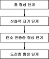
본 발명의 과제를 해결하기 위한, 일 실시예에 따른 금속 집전체는 표면에 홈이 형성된 금속 기재, 상기 금속 기재에 형성된 탄소 완충층, 및 상기 탄소 완충층 상에 형성된 도전층을 포함하는 것을 특징으로 한다. According to an aspect of the present invention, a metal current collector includes a metal substrate having a groove formed on a surface thereof, a carbon buffer layer formed on the metal substrate, and a conductive layer formed on the carbon buffer layer. .
상기 금속 기재는 알루미늄, 스텐레스, 티타늄, 탄탈, 니오브, 구리, 니켈, 및 이들의 합금으로 이루어진 그룹으로부터 선택되는 1종 이상일 수 있다. The metal substrate may be at least one selected from the group consisting of aluminum, stainless steel, titanium, tantalum, niobium, copper, nickel, and alloys thereof.
상기 금속 기재는 알루미늄 또는 이의 합금이 보다 바람직하게 사용될 수 있다. As the metal substrate, aluminum or an alloy thereof may be more preferably used.
상기 금속 기재는 시트상의 호일, 에칭된 호일(etched foil), 익스팬디드 금속(expanded metal), 펀칭된 금속(punched metal), 그물, 및 발포체 형태를 가지는 것일 수 있다. The metal substrate may be in the form of sheet-like foils, etched foils, expanded metals, punched metals, nets, and foams.
상기 금속 기재에 형성된 홈은 1.0~5.0㎛의 깊이를 가지는 것이 바람직하다. It is preferable that the groove formed in the said metal substrate has a depth of 1.0-5.0 micrometers.
상기 금속 기재에 형성된 홈 간 간격은 5.0~10.0㎛인 것이 바람직하다. It is preferable that the space | interval between grooves formed in the said metal base material is 5.0-10.0 micrometers.
상기 탄소 완충층은 탄소(C) 함유 재료를 이용하는 것이 바람직하다. It is preferable that a carbon (C) containing material is used for the said carbon buffer layer.
상기 탄소 완충층은 상기 금속 기재에 형성된 홈 간의 요철부의 일부 또는 전부에 형성될 수 있다. The carbon buffer layer may be formed on some or all of the uneven portions between the grooves formed in the metal substrate.
상기 도전층은 super-p, 흑연(graphite), 코크스(cokes), 활성탄, 및 카본 블랙으로 이루어진 그룹으로부터 선택되는 1종 이상의 도전성 카본을 이용하는 것이 바람직하다.
The conductive layer preferably uses at least one conductive carbon selected from the group consisting of super-p, graphite, cokes, activated carbon, and carbon black.
본 발명은 또한, 다른 과제를 해결하기 위하여 금속 기재의 표면에 홈을 형성시키는 제1단계, 상기 금속 기재에 형성된 자연산화막을 제거하는 제2단계, 상기 자연산화막이 제거된 금속 기재에 탄소 완충층을 형성하는 제3단계, 및 상기 탄소 완충층 상에 도전층을 형성하는 제4단계를 포함하는 금속 집전체의 제조방법을 제공하는 것을 특징으로 한다. The present invention also provides a carbon buffer layer on a metal substrate from which the first step of forming a groove on the surface of the metal substrate, the second step of removing the natural oxide film formed on the metal substrate, the natural oxide film is removed in order to solve other problems It provides a method for producing a metal current collector comprising a third step of forming, and a fourth step of forming a conductive layer on the carbon buffer layer.
상기 홈은 상기 금속 기재의 표면을 에칭 및 국부 부식시켜 형성시킬 수 있다. The groove may be formed by etching and localized corrosion of the surface of the metal substrate.
상기 자연산화막의 제거는 인산, 황산, 질산, 염산, 아세트산, 탄산, 트리플로로아세트산, 옥살산, 불산, 붕산, 과염소산, 차아염소산 및 이들의 혼합물로 이루어진 그룹으로부터 선택되는 1종 이상의 산 용액으로 처리하는 것일 수 있다. The removal of the natural oxide film is treated with at least one acid solution selected from the group consisting of phosphoric acid, sulfuric acid, nitric acid, hydrochloric acid, acetic acid, carbonic acid, trifluoroacetic acid, oxalic acid, hydrofluoric acid, boric acid, perchloric acid, hypochlorous acid and mixtures thereof. It may be.
상기 자연산화막의 제거는 수산화칼륨, 수산화나트륨, 수산화리튬, 암모니아수, 및 이들의 혼합물로 이루어진 그룹으로부터 선택되는 1종 이상의 염기성 용액으로 처리하는 것일 수 있다. Removal of the natural oxide film may be treatment with one or more basic solutions selected from the group consisting of potassium hydroxide, sodium hydroxide, lithium hydroxide, ammonia water, and mixtures thereof.
상기 탄소 완충층은 이온 주입(implantation) 혹은 탄소 증착 후 고온 확산에 의한 방법으로 형성시키는 것일 수 있다.
The carbon buffer layer may be formed by ion implantation or high temperature diffusion after carbon deposition.
또한, 본 발명은 상기 금속 집전체를 구비한 전기 화학 커패시터를 제공할 수 있다. In addition, the present invention can provide an electrochemical capacitor having the metal current collector.
상기 금속 집전체는 양극 및/또는 음극 중에서 선택되는 어느 하나, 및 모두에 사용될 수 있다.
The metal current collector may be used for any one selected from a positive electrode and / or a negative electrode, and both.
추가로 본 발명은 상기 금속 집전체에 전극 활물질을 포함하는 전극을 구비한 전기 화학 커패시터를 제공할 수 있다. In addition, the present invention may provide an electrochemical capacitor having an electrode including an electrode active material in the metal current collector.
상기 전극 활물질은 활성탄, 탄소나노튜브(CNT), 그라파이트, 카본 에어로겔, 폴리아크릴로니트릴(PAN), 탄소나노섬유(CNF), 활성화 탄소나노섬유(ACNF), 기상성장 탄소섬유(VGCF), 및 그래핀으로 이루어진 그룹으로부터 선택되는 1종 이상의 탄소 재료가 바람직하다. The electrode active material is activated carbon, carbon nanotubes (CNT), graphite, carbon aerogels, polyacrylonitrile (PAN), carbon nanofibers (CNF), activated carbon nanofibers (ACNF), vapor-grown carbon fibers (VGCF), and Preference is given to at least one carbon material selected from the group consisting of graphene.
상기 전극 활물질은 비표면적 1,500~3,000 ㎡/g인 활성탄을 가장 바람직하게 사용할 수 있다.
The electrode active material may most preferably use activated carbon having a specific surface area of 1,500 to 3,000 m 2 / g.
본 발명에 따르면, 금속 기재의 표면에 홈을 형성시키고, 상기 금속 기재에 탄소 완충층, 및 도전층을 포함하는 금속 집전체는 접합강도는 크고, 접촉저항이 낮은 특성을 가진다. According to the present invention, a metal current collector including a groove formed on a surface of the metal substrate and including a carbon buffer layer and a conductive layer on the metal substrate has a high bonding strength and low contact resistance.
따라서, 상기 금속 집전체로부터 제조된 전극은 낮은 ESR 값을 가지며, 이를 구비한 전기 화학 캐패시터는 고전압에서의 고율 충방전이 가능하여 사이클 수명이 증가하는 효과를 기대할 수 있다. 또한, 탄소 완충층의 형성으로 접착강도나 내구성 같은 기계적 특성도 동시에 만족시킬 수 있다.
Therefore, the electrode manufactured from the metal current collector has a low ESR value, and the electrochemical capacitor having the same can be expected to have an effect of increasing cycle life by enabling high rate charge / discharge at high voltage. In addition, the formation of the carbon buffer layer can simultaneously satisfy mechanical properties such as adhesive strength and durability.
도 1은 본 발명에 따른 금속 집전체의 구조이고,
도 2는 본 발명에 따른 금속 집전체의 제조 과정을 나타낸 것이다.
도 3은 본 발명에 따른 금속 집전체의 제조 과정의 모식도이다.1 is a structure of a metal current collector according to the present invention,
Figure 2 shows the manufacturing process of a metal current collector according to the present invention.
3 is a schematic diagram of a manufacturing process of a metal current collector according to the present invention;
이하에서 본 발명을 더욱 상세하게 설명하면 다음과 같다. Hereinafter, the present invention will be described in more detail.
본 명세서에서 사용된 용어는 특정 실시예를 설명하기 위하여 사용되며, 본 발명을 제한하기 위한 것이 아니다. 본 명세서에서 사용된 바와 같이, 단수 형태는 문맥상 다른 경우를 분명히 지적하는 것이 아니라면, 복수의 형태를 포함할 수 있다. 또한, 본 명세서에서 사용되는 경우 "포함한다(comprise)" 및/또는 "포함하는(comprising)"은 언급한 형상들, 숫자, 단계, 동작, 부재, 요소 및/또는 이들 그룹의 존재를 특정하는 것이며, 하나 이상의 다른 형상, 숫자, 동작, 부재, 요소 및/또는 그룹들의 존재 또는 부가를 배제하는 것이 아니다.
The terminology used herein is for the purpose of describing particular embodiments only and is not intended to be limiting of the invention. As used herein, the singular forms "a", "an" and "the" may include the plural forms as well, unless the context clearly indicates otherwise. Also, as used herein, "comprise" and / or "comprising" specifies the presence of the mentioned shapes, numbers, steps, actions, members, elements and / or groups of these. It is not intended to exclude the presence or the addition of one or more other shapes, numbers, acts, members, elements and / or groups.
본 발명은 전기 화학 커패시터에 사용되는 금속 집전체와 이의 제조방법, 및 이를 구비한 전기 화학 커패시터에 관한 것이다. The present invention relates to a metal current collector used in an electrochemical capacitor, a method of manufacturing the same, and an electrochemical capacitor having the same.
본 발명의 일 실시예에 따른 금속 집전체는 다음 도 1에 나타낸 바와 같으며, 표면에 홈(11)이 형성된 금속 기재(10), 상기 금속 기재(10)에 형성된 탄소 완충층(20), 및 상기 탄소 완충층(20) 상에 형성된 도전층(30)을 포함하는 것을 특징으로 한다. The metal current collector according to the embodiment of the present invention is as shown in FIG. 1, wherein the
즉, 금속 기재(10) 표면을 국부적으로 부식시키면, 부식된 자리에 홈(11)이 형성되어 나노 막대 형태의 배열(nanorod array)을 만들어 집전체의 표면적을 증가시킬 수 있다. That is, when the surface of the
상기 금속 기재(10) 표면을 국부적으로 부식시키는 경우, 금속 자체에 형성되어 있는 3중 교차 라인(triple junction line)을 따라 처리할 수도 있고, 임의의 지점들을 에칭시켜 처리할 수도 있다. When the surface of the
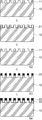
도 1에서 상기 홈(11)은 약 2~5㎛ 깊이의 트렌치 형태로 나타냈으나, 이는 다양한 형태 중 하나의 형태를 나타낸 것으로, 형성된 홈의 형태가 특별히 한정되지 않고, 예를 들어, 둥근 원기둥 형태, 원뿔 형태 등을 가질 수도 있다. 이러한 홈의 형태는 부식에 사용되는 부식액의 종류, 농도, 및 온도 등을 조절하게 소정의 형태를 가지도록 할 수 있다.In FIG. 1, the
상기 금속 기재에 형성된 홈 간 간격은 5.0~10.0㎛인 것이 바람직하다. 3중 교차 라인(Triple junction line)과 같이 특정 조건을 가지지 않게 되면, 즉, 일반적인 경우 간격을 조밀하게 하기 위해서 산의 농도나 공정조건을 가혹하게 해야 된다. 이 경우, 집전체의 기계적 특성저하의 문제가 발생하여 셀 제작을 위한 공정성이 많이 떨어지게 된다. 반대로 너무 간격이 클 경우, 전극층과 집전체와의 실제 접촉면적이 감소하여 저항이 다시 증가하기 때문이다. It is preferable that the space | interval between grooves formed in the said metal base material is 5.0-10.0 micrometers. If there are no specific conditions, such as triple junction lines, that is, in general, the concentration of the acid or the processing conditions must be severe to close the gap. In this case, a problem of deterioration in the mechanical properties of the current collector occurs, and the processability for manufacturing the cell is inferior. On the contrary, when the spacing is too large, the actual contact area between the electrode layer and the current collector decreases and the resistance increases again.
이때 사용되는 부식액은 염산, 인산, 불화규소산 및 황산으로 이루어진 그룹으로부터 선택되는 1종 이상일 수 있으나, 이에 한정되는 것은 아니다. At this time, the corrosion solution used may be one or more selected from the group consisting of hydrochloric acid, phosphoric acid, silicon fluoride acid and sulfuric acid, but is not limited thereto.
또한, 상기 국부 부식시 온도는 50~90℃의 온도에서 수행하는 것이 공정성을 고려하여 일정 시간 안에 균일한 에칭 피트를 형성시킬 수 있다는 측면에서 바람직하나, 특별히 이에 한정되는 것은 아니다. In addition, the local corrosion temperature is preferably carried out at a temperature of 50 ~ 90 ℃ in consideration of fairness in terms of forming a uniform etching pit within a predetermined time, but is not particularly limited thereto.
상기와 같이 금속 기재 표면에 홈을 형성함으로써, 집전체의 표면적이 증가하게 되고 이는 실제 전극과의 유효접촉면적을 증가시켜서 접촉저항을 낮추는 효과를 가진다. 또한 잘 배열된 상기 홈(11) 크기의 조절을 통해 빠른 이온의 확산이 용이하여 충방전 속도도 향상시킬 수 있다.
By forming the groove on the surface of the metal substrate as described above, the surface area of the current collector is increased, which has the effect of lowering the contact resistance by increasing the effective contact area with the actual electrode. In addition, through the adjustment of the size of the
본 발명에서 사용되는 금속 기재로는 알루미늄, 스텐레스, 티타늄, 탄탈, 니오브, 구리, 니켈, 및 이들의 합금으로 이루어진 그룹으로부터 선택되는 1종 이상일 수 있으며, 이 중에서 알루미늄 또는 이의 합금이 보다 바람직하게 사용될 수 있다. The metal substrate used in the present invention may be at least one selected from the group consisting of aluminum, stainless steel, titanium, tantalum, niobium, copper, nickel, and alloys thereof, of which aluminum or an alloy thereof is more preferably used. Can be.
상기 금속 기재는 시트상의 호일, 에칭된 호일(etched foil), 익스팬디드 금속(expanded metal), 펀칭된 금속(punched metal), 그물, 및 발포체 형태를 가지는 것일 수 있으며, 금속 기재의 형태 또한 특별히 한정되지 않는다.
The metal substrate may be in the form of a sheet-like foil, etched foil, expanded metal, punched metal, net, and foam form, and the form of the metal substrate may also be particularly It is not limited.
또한, 본 발명에 따른 금속 집전체는 홈(11)이 형성된 상기 금속 기재(10) 에 탄소 완충층(20)을 포함한다. In addition, the metal current collector according to the present invention includes a
통상적으로, 상기 알루미늄과 같은 금속은 대기에 노출시키면 즉시 산화되어, 상기 홈이 형성된 금속 기재에도 자연산화막이 생성된다. 그러나, 이러한 자연산화막은 절연막이기 때문에 집전체와 활물질층 간의 전기 저항을 증대시키는 문제가 있다. 또한, 상기와 같이 금속 기재 표면에 홈을 형성하게 되는 경우, 상기 홈을 따라서 상대적으로 두꺼운 자연산화막의 형성도 배제할 수 없게 되므로 부도체인 자연산화막에 의한 전기전도도의 감소효과도 생기게 된다. 이는 고전압, 고전류로 가게 될 수록 이로 인한 성능저하의 효과가 더욱 두드러지게 된다.Typically, a metal such as aluminum is oxidized immediately upon exposure to the atmosphere, so that a natural oxide film is also formed on the grooved metal substrate. However, since the natural oxide film is an insulating film, there is a problem of increasing the electrical resistance between the current collector and the active material layer. In addition, when the groove is formed on the surface of the metal substrate as described above, the formation of a relatively thick natural oxide film along the groove cannot be excluded, so that the electrical conductivity caused by the non-conductive natural oxide film is also generated. The higher the voltage, the higher the current, the more noticeable the effect of this performance degradation.
따라서, 본 발명에서는 전기전도도에 좋지 않은 영향을 미치는 상기 자연산화막을 제거한 다음, 그 위에 탄소 완충층(20)을 형성한다. Therefore, in the present invention, the
상기 탄소 완충층(20)은 이온 주입 등의 방법에 의해서 탄소 함유 재료를 인위적으로 홈이 형성된 금속 기재 표면에 확산시키는 것으로, 다음 도 1에서와 같이, 상기 탄소 완충층(20)은 상기 금속 기재(10)에 형성된 홈(11) 간의 요철부의 일부 또는 전부를 감싸는 영역에 형성될 수 있다. The
이는, 상기 탄소 함유 재료를 확산시키는 경우, 금속 집전체를 구성하는 금속 기재(10)의 성분 중의 일부와 탄소 재료가 상기 탄소 완충층(20)에 공존하여 상기 홈 간의 요철부에 침투되어 형성되는 것으로 예상할 수 있다. 따라서, 상기 탄소 완충층(20)에는 전극 활물질로 사용되는 탄소 재료와 동일한 성분이 함유되어 있기 때문에 전극 활물질층과의 접착 강도를 향상시킬 수 있게 된다.
This means that when the carbon-containing material is diffused, some of the components of the
또한, 본 발명에 따른 금속 집전체는 상기 탄소 완충층(20) 위에 도전층(30)을 포함한다. In addition, the metal current collector according to the present invention includes a
상기 도전층(30)은 충전된 전하의 빠른 방전을 극대화 시키며, 집전체와 활물질층 계면에서의 저항을 낮추는 역할을 한다. The
따라서, 기존의 단순히 표면 에칭된 금속 집전체에 비해서 비표면적이 넓고, 전기전도도에 방해가 되는 알루미늄 산화막을 제거 후 도전층을 형성시키기 때문에 충전된 전하를 외부로 보낼 때 발생하는 접촉저항이 매우 작게 된다. Therefore, the specific surface area is larger than that of the conventional simply etched metal current collector, and since the conductive layer is formed after removing the aluminum oxide film which hinders the electrical conductivity, the contact resistance generated when sending the charged electric charge to the outside is very small. do.
이러한 도전층 재료로는 전기 저항이 낮은 재질의 것이 바람직한데, 예를 들어, 전기 저항이 10 S/cm 이상, 바람직하기로는 100 S/cm 이상인 재료를 사용할 수 있다. 이러한 재료의 예로는, super-p, 흑연(graphite), 코크스(cokes), 활성탄, 및 카본 블랙으로 이루어진 그룹으로부터 선택되는 1종 이상의 도전성 카본을 들 수 있으나, 이에 한정되는 것은 아니다.As the conductive layer material, a material having a low electrical resistance is preferable. For example, a material having an electrical resistance of 10 S / cm or more, preferably 100 S / cm or more can be used. Examples of such materials include, but are not limited to, one or more conductive carbons selected from the group consisting of super-p, graphite, cokes, activated carbon, and carbon black.
본 발명의 도전층(30)은 탄소 완충층(20) 상에 형성되고, 상기 탄소 완충층(20)은 홈(11)이 형성된 금속 부재(10)에 형성되는 것이다. 따라서 상기 도전층(30)은 상기 탄소 완충층(20)의 형상을 따라 금속 부재 표면에 형성된 홈의 형상대로 형성될 수도 있고, 금속 부재 표면은 물론 홈 부분에도 매립되도록 형성될 수도 있다. 따라서, 상기 도전층의 두께는 금속 부재의 홈 표면으로부터 1.0~5.0㎛인 것이 단위부피당 전극의 정전용량감소를 크게 하지 않으면서 전기전도도를 극대화 할 수 있다. 두께는 얇을수록 좋으나, 1.0㎛ 이하일 경우 프레스 공정시 어려움이 있어서 이보다 얇게 하는 것은 바람직하지 않으나, 그 두께가 특별히 한정되는 것은 아니다.
The
본 발명에 따른 금속 집전체의 제조방법을 다음 도 2와 3을 참조하여 이하에서 상세히 설명한다. A method of manufacturing a metal current collector according to the present invention will be described in detail below with reference to FIGS. 2 and 3.
본 발명에 따른 금속 집전체는 다음 도 2에서와 같이, 금속 기재(10)의 표면에 홈(11)을 형성시키는 제1단계(S1), 상기 금속 기재(10)에 형성된 자연산화막(21)을 제거하는 제2단계(S2), 상기 자연산화막(21)이 제거된 금속 기재(10)에 탄소 완충층(20)을 형성하는 제3단계(S3), 및 상기 탄소 완충층(20) 상에 도전층(30)을 형성하는 제4단계를 거쳐 제조할 수 있다. In the metal current collector according to the present invention, as shown in FIG. 2, the first step S1 of forming the
먼저 첫 번째 단계(S1)는, 상기 금속 기재(10) 표면의 일부 지점을 에칭시키거나, 또는 3중 교차 라인들을 따라 국부 부식시켜 홈(11)을 형성시키는 단계이다. 3중 교차 라인들은 사용되는 각 금속 기재(10)가 가지는 고유한 특성이기 때문에, 상기 라인을 따라 국부적으로 부식시키거나, 표면의 일부 지점을 따라 에칭시키면, 부식 및 에칭된 부위에 일정한 간격의 홈(11)이 형성된다. First step S1 is to etch some points on the surface of the
본 발명의 도면에서는 상기 홈(11)을 트렌치 형태로 나타냈으나, 요철 형태, 및 원기둥 형태 등을 가질 수도 있으며, 상기 홈(11)의 형태가 특별히 한정되는 것은 아니다. 이러한 홈의 형태는 부식에 사용되는 부식액의 종류, 농도, 및 온도 등을 조절하게 소정의 형태를 가지도록 할 수 있다.In the drawings of the present invention, the
한편, 상기 홈(11)이 형성된 금속 기재(10)를 공기 중에 노출시키게 되면 상기 금속 기재(10)의 특성상 쉽게 산화되어, 상기 금속 기재의 표면에 얇은 자연산화막(21)이 생성된다. 상기 자연산화막(21)은 인위적인 외부 수단에 의한 것이 아니라, 대기 중에 노출될 때 자연적으로 생성되는 것이므로 자연산화막이라 한다. 예를 들어, 상기 금속 기재(10)로 알루미늄 및 이의 합금을 사용하는 경우, 상기 금속 기재 표면이 자연 산화되어 표면에 알루미늄 옥사이드(Al2O3)가 생성된다. Meanwhile, when the
그러나, 이러한 자연산화막(21)은 금속 집전체와 활물질층 간의 저항을 높이는 문제가 있으므로, 본 발명에서는 두 번째 단계(S2)로 상기 자연산화막을 제거시키는 과정을 거친다.However, since the
상기 자연산화막(21) 제거 과정을 거치게 되면, 상기 첫 번째 단계의 홈이 형성된 금속 기재 상태로 된다. When the
본 발명의 일 실시예에 따르면, 상기 자연산화막(21)은 적절한 용액에 침지시켜 제거하는 화학적인 방법, 또는 에칭 방법을 이용할 수 있다. According to an embodiment of the present invention, the
상기 자연산화막 제거에 사용되는 용액의 예로는, 인산, 황산, 질산, 염산, 아세트산, 탄산, 트리플로로아세트산, 옥살산, 불산, 붕산, 과염소산, 차아염소산 및 이들의 혼합물로 이루어진 그룹으로부터 선택되는 1종 이상의 산 용액이 바람직하다.Examples of the solution used to remove the natural oxide film, 1 selected from the group consisting of phosphoric acid, sulfuric acid, nitric acid, hydrochloric acid, acetic acid, carbonic acid, trifluoroacetic acid, oxalic acid, hydrofluoric acid, boric acid, perchloric acid, hypochlorous acid and mixtures thereof. Preference is given to acid solutions of at least species.
또한 본 발명의 다른 일 실시예에 따르면, 상기 자연산화막의 제거는 수산화칼륨, 수산화나트륨, 수산화리튬, 암모니아수, 및 이들의 혼합물로 이루어진 그룹으로부터 선택되는 1종 이상의 염기성 용액을 이용할 수도 있다. In addition, according to another embodiment of the present invention, the removal of the natural oxide film may use at least one basic solution selected from the group consisting of potassium hydroxide, sodium hydroxide, lithium hydroxide, ammonia water, and mixtures thereof.
또한, 에칭법을 이용하는 경우, 드라이 에칭이 보다 바람직한데, 예를 들어, 아르곤, 및 질소와 같은 다양한 불활성 가스 이온을 이용하여 스퍼터 에칭(sputter etching)시킬 수 있다. 그러나, 상기 에칭법이 스퍼터 장치에 한정되지 않고, 다른 에칭법을 사용하는 것도 무방하다.
In addition, when etching is used, dry etching is more preferable. For example, sputter etching may be performed using various inert gas ions such as argon and nitrogen. However, the etching method is not limited to the sputtering device, and other etching methods may be used.
세 번째 단계(S3)에서는, 자연산화막(21)이 제거된 금속 기재(10)에 탄소 완충층(20)을 형성시킨다. In the third step S3, the
상기 탄소 완충층(20)은 탄소 함유 재료를 이온 주입, 탄소층을 증착 후에 고온에서 확산시키는 등의 방법으로 수행되는 것일 수 있으나, 그 방법이 특별히 한정되는 것은 아니다. The
상기 탄소 완충층(20)은 금속 기재(10)에 형성된 홈(11) 간의 요철부의 일부 또는 전부를 감싸는 영역에 형성될 수 있다. 또한, 상기 탄소 완충층(20)에는 금속 집전체를 구성하는 금속 기재(10)의 성분 중의 일부와 탄소 함유 재료가 혼합되어 있다.
The
마지막으로, 상기 탄소 완충층(20)에 도전층(30)을 형성하는 단계(S4)이다. 상기 도전층(30)을 형성하는 방법은 특별히 한정되지 않고, 예를 들면 스퍼터링(spattering)법, 이온 도금(ion plating, IP)법, 아크 이온 도금(arc ion plating, AIP)법 등의 물리적 증착(PVD); 또는 플라즈마 CVD 법 등의 화학 증착(CVD)을 이용할 수 있다. 또한, 도전층 형성 재료를 슬러리 형태로 제조하여, 이를 코팅시켜 형성할 수도 있다. Finally, the
본 발명의 일 실시예에 따르면, 상기 도전층(30)은 홈(11)이 형성된 금속 기재(10)를 완전히 덮을 수 있도록, 홈의 매립부를 채움과 동시에 상기 홈의 최상부로부터 1.0~5.0㎛의 두께로 형성시키는 것이 바람직하다. According to the exemplary embodiment of the present invention, the
또한, 본 발명의 다른 일 실시예에 따르면, 상기 도전층(30)은 홈(11)이 형성된 형태를 따라 매립된 홈(11) 영역에는 코팅되지 않고, 홈(11) 형상대로 형성될 수도 있다. In addition, according to another embodiment of the present invention, the
상기 도전층(30) 형성을 위한 재료로는 super-p, 흑연(graphite), 코크스(cokes), 활성탄, 및 카본 블랙으로 이루어진 그룹으로부터 선택되는 1종 이상의 도전성 분말이 바람직하다. The material for forming the
상기 도전층(30)의 형성으로 집전체의 전기적 저항을 낮출 수 있고, 충전된 전하의 빠른 방전을 극대화시킬 수 있다.
The formation of the
또한, 본 발명은 상기 금속 집전체를 구비한 전기 화학 커패시터를 제공할 수 있다. 상기 금속 집전체는 양극 및/또는 음극 중에서 선택되는 어느 하나 또는 모두에 사용될 수 있다.
In addition, the present invention can provide an electrochemical capacitor having the metal current collector. The metal current collector may be used for any one or both selected from a positive electrode and / or a negative electrode.
본 발명에 따른 전기 화학 커패시터는 상기 집전체 상에 전극 활물질 슬러리 조성물을 도포시킨 전극, 분리막, 및 전해액을 포함한다. The electrochemical capacitor according to the present invention includes an electrode, a separator, and an electrolyte in which an electrode active material slurry composition is coated on the current collector.
전극 활물질 슬러리 조성물은 전극 활물질, 도전재, 바인더, 용매 및 기타 첨가제를 혼합 및 교반시켜 제조할 수 있다. The electrode active material slurry composition may be prepared by mixing and stirring an electrode active material, a conductive material, a binder, a solvent, and other additives.
본 발명에 따른 전극 활물질은 활성탄, 탄소나노튜브(CNT), 그라파이트, 카본 에어로겔, 폴리아크릴로니트릴(PAN), 탄소나노섬유(CNF), 활성화 탄소나노섬유(ACNF), 기상성장 탄소섬유(VGCF), 및 그래핀으로 이루어진 그룹으로부터 선택되는 1종 이상의 탄소 재료가 바람직하게 사용될 수 있다. Electrode active material according to the present invention is activated carbon, carbon nanotubes (CNT), graphite, carbon aerogels, polyacrylonitrile (PAN), carbon nanofibers (CNF), activated carbon nanofibers (ACNF), vapor-grown carbon fibers (VGCF ), And at least one carbon material selected from the group consisting of graphene can be preferably used.
본 발명의 바람직한 일 실시예에 따르면, 상기 전극 활물질 중에서 비표면적 1,500~3,000 ㎡/g인 활성탄을 사용하는 것이 가장 바람직하다. According to a preferred embodiment of the present invention, it is most preferable to use activated carbon having a specific surface area of 1,500 to 3,000 m 2 / g among the electrode active materials.
또한, 도전재로서 슈퍼-p(super-p), 케첸 블랙, 아세틸렌 블랙, 카본 블랙, 그라파이트와 같은 도전성 분말을 포함할 수 있다. In addition, the conductive material may include a conductive powder such as super-p, Ketjen black, acetylene black, carbon black, graphite.
상기 바인더 수지의 예를 들면, 폴리테트라플로로에틸렌(PTFE), 폴리비닐리덴플로라이드(PVdF) 등의 불소계 수지; 폴리이미드, 폴리아미드이미드, 폴리에딜렌(PE), 폴리프로필렌(PP) 등의 열가소성수지; 카복시메틸셀룰로우즈(CMC) 등의 셀룰로오즈계 수지; 스타이렌-부타디엔 고무(SBR) 등의 고무계 수지 및 이들의 혼합물 중에서 선택되는 1종 이상을 사용할 수 있으나, 특별히 이에 한정되지 않으며, 통상의 전기 화학 커패시터에 사용되는 모든 바인더 수지를 사용해도 무방하다. Examples of the binder resin include fluororesins such as polytetrafluoroethylene (PTFE) and polyvinylidene fluoride (PVdF); Thermoplastic resins such as polyimide, polyamideimide, polyedylene (PE) and polypropylene (PP); Cellulose-based resins such as carboxymethylcellulose (CMC); One or more selected from rubber-based resins such as styrene-butadiene rubber (SBR) and mixtures thereof may be used, but is not particularly limited thereto, and any binder resin used in a conventional electrochemical capacitor may be used.
또한, 상기 전극은 본 발명에 따라 제조된 집전체 상에 전극 활물질 조성물을 소정의 두께로 도포시켜 제조할 수 있으며, 전극 활물질 조성물의 도포 방법은 특별히 한정되지 않는다. In addition, the electrode may be prepared by applying the electrode active material composition to a current collector prepared according to the present invention to a predetermined thickness, the coating method of the electrode active material composition is not particularly limited.
또한, 전극 활물질, 도전재, 및 용매 혼합물을 상기 바인더 수지를 이용하여 시트 형상으로 성형하거나, 압출방식으로 압출된 성형 시트를 집전체에 도전성 접착제를 이용하여 접합할 수도 있다.
In addition, the electrode active material, the conductive material, and the solvent mixture may be molded into a sheet shape using the binder resin, or the molded sheet extruded by the extrusion method may be bonded to the current collector using a conductive adhesive.
본 발명에 따른 분리막은 종래 전기이중층 캐패시터나 리튬 이온 전지에 사용되는 모든 재질의 재료를 이용할 수 있으며, 예를 들어, 폴리에틸렌(PE), 폴리프로필렌(PP), 폴리비닐리덴플로라이드(PVDF), 폴리비닐리덴클로라이드, 폴리 아크릴로니트릴(PAN), 폴리아크릴아미드(PAAm), 폴리테트라플루오로 에틸렌(PTFE), 폴리설폰, 폴리에테르술폰(PES), 폴리카보네이트(PC), 폴리아미드(PA), 폴리이미드(PI), 폴리에틸렌옥사이드(PEO), 폴리프로필렌옥사이드(PPO), 셀룰로오스계 고분자, 및 폴리아크릴계 고분자로 이루어진 그룹으로부터 선택되는 1종 이상의 고분자로부터 제조된 미세 다공성 필름을 들 수 있다. 또한, 상기 다공성 필름을 중합시킨 다층 필름도 이용할 수 있으며, 이 중에서 셀룰로오스계 고분자가 바람직하게 사용될 수 있다. The separator according to the present invention may use materials of any material conventionally used in an electric double layer capacitor or a lithium ion battery. For example, polyethylene (PE), polypropylene (PP), polyvinylidene fluoride (PVDF), Polyvinylidene chloride, poly acrylonitrile (PAN), polyacrylamide (PAAm), polytetrafluoro ethylene (PTFE), polysulfone, polyethersulfone (PES), polycarbonate (PC), polyamide (PA) And microporous films prepared from one or more polymers selected from the group consisting of polyimide (PI), polyethylene oxide (PEO), polypropylene oxide (PPO), cellulose polymers, and polyacrylic polymers. A multilayer film obtained by polymerizing the porous film may also be used, and among them, a cellulose-based polymer may be preferably used.
상기 분리막의 두께는 약 15~35㎛가 바람직하나, 이에 한정되는 것은 아니다.
The thickness of the separator is preferably about 15 ~ 35㎛, but is not limited thereto.
본 발명의 전해액은 TEABF4, TEMABF4 등의 비리튬염; 스파이로계 염; 및 LiPF6, LiBF4, LiCLO4, LiN(CF3 SO2)2, CF3SO3Li, LiC(SO2CF3)3, LiAsF6 및 LiSbF6 로 이루어진 그룹으로부터 선택되는 1종 이상의 리튬염 중에서 선택되는 1종 이상을 포함하는 유기 전해액을 사용할 수 있으나, 이에 한정되는 것은 아니다. Electrolyte solution of this invention is non-lithium salt, such as TEABF 4 and TEMABF 4 ; Spiro salts; And at least one lithium salt selected from the group consisting of LiPF 6 , LiBF 4 , LiCLO 4 , LiN (CF 3 SO 2 ) 2 , CF 3 SO 3 Li, LiC (SO 2 CF 3 ) 3 , LiAsF 6 and LiSbF 6 An organic electrolyte including one or more selected from among them may be used, but is not limited thereto.
상기 전해액의 용매로는 아크릴로니크릴, 에틸렌 카보네이트, 프로필렌 카보네이트, 디메틸 카보네이트, 에틸메틸 카보네이트, 설포란 및 디메톡시에탄으로 이루어진 그룹으로부터 선택되는 1종 이상이나, 이에 한정되는 것은 아니다. 전해액 속의 전해질 염의 농도는 0.1~2.5mol/L, 0.5~2mol/L이 바람직하다.The solvent of the electrolyte solution is one or more selected from the group consisting of acrylonitrile, ethylene carbonate, propylene carbonate, dimethyl carbonate, ethylmethyl carbonate, sulfolane and dimethoxyethane, but is not limited thereto. The concentration of the electrolyte salt in the electrolyte is preferably 0.1 to 2.5 mol / L and 0.5 to 2 mol / L.
본 발명의 전기 화학 캐패시터의 케이스(외장재)로는, 이차 전지 및 전기이중층 캐패시터에 통상적으로 사용되는 알루미늄을 포함하는 라미네이트 필름을 사용하는 것이 바람직하나, 특별히 이에 한정되는 것은 아니다. As the case (exterior material) of the electrochemical capacitor of the present invention, it is preferable to use a laminate film containing aluminum, which is commonly used in secondary batteries and electric double layer capacitors, but is not particularly limited thereto.
이하에서 본 발명의 바람직한 실시예를 상세히 설명하기로 한다. 이하의 실시예는 본 발명을 예시하기 위한 것일 뿐, 본 발명의 범위가 이들 실시예에 의해 제한되는 것으로 해석되어서는 안 된다. 또한, 이하의 실시예에서는 특정 화합물을 이용하여 예시하였으나, 이들의 균등물을 사용한 경우에 있어서도 동등 유사한 정도의 효과를 발휘할 수 있음은 당업자에게 자명하다.
Hereinafter, preferred embodiments of the present invention will be described in detail. The following examples are intended to illustrate the present invention, but the scope of the present invention should not be construed as being limited by these examples. In the following examples, specific compounds are exemplified. However, it is apparent to those skilled in the art that equivalents of these compounds can be used in similar amounts.
실시예Example 1 : 금속 1: metal 집전체의Whole 제조 Produce
25㎛ 두께의 알루미늄 원박을 준비한 후, 아세톤-에틸알콜의 순서로 각각 20분간 초음파 세척을 실시하였다. 상기 세척한 알루미늄 박을 45℃에서 60초간 불화규소산(H2SiF6)으로 처리하여 국부 부식시켜 홈을 형성시켰다. 상기 형성된 홈은 1.0~5.0㎛의 깊이를 가지며, 홈 간 간격은 5.0~10.0㎛ 였다.After preparing a 25-micrometer-thick aluminum foil, ultrasonic cleaning was performed for 20 minutes in the order of acetone-ethyl alcohol. The washed aluminum foil was treated with silicon fluoride (H 2 SiF 6 ) at 45 ° C. for 60 seconds to locally corrode to form grooves. The formed groove had a depth of 1.0 ~ 5.0㎛, the interval between the grooves was 5.0 ~ 10.0㎛.
그 다음, 전해 교류 에칭을 35℃에서 1.0M의 염산(HCl)+ 0.01M의 황산(H2SO4) 혼합용액에서 2분간 실시하여 자연산화막을 제거하였다. Then, electrolytic alternating current etching was performed at 35 ° C. for 2 minutes in 1.0 M hydrochloric acid (HCl) +0.01 M sulfuric acid (H 2 SO 4 ) mixed solution to remove the native oxide film.
상기 자연산화막이 제거된 알루미늄 박에 C 이온 임플란테이션 장비를 이용하여 표면에 탄소완충층을 ~1 ㎛ 깊이로 형성시켰다. 그 다음, Super-P 80g, 바인더로써 CMC 3.5g, SBR 5.0g을 물 155g에 혼합 및 교반시켜 도전층 슬러리를 제조한 후, 코터(comma coater)를 이용하여 상기 탄소완충층 위에 도포함으로써 도전층을 형성시켰다. A carbon buffer layer was formed at a depth of ˜1 μm on the surface of the aluminum foil from which the natural oxide film was removed using a C ion implantation apparatus. Then, a conductive layer slurry was prepared by mixing and stirring 80 g of Super-P, 3.5 g of CMC, and 5.0 g of SBR as a binder to 155 g of water, and then applying a coater on the carbon buffer layer using a coater to coat the conductive layer. Formed.
그 후 다시 아세톤-에틸알콜의 순서로 20분간 초음파 세척을 실시하여 세척을 하여 전극을 도포할 집전체를 준비하였다.
Thereafter, ultrasonic cleaning was performed for 20 minutes in the order of acetone-ethyl alcohol, followed by washing to prepare a current collector to apply the electrode.
비교예Comparative example 1 One
두께 20㎛의 알루미늄 에칭박을 금속 집전체로 사용하였다.
An aluminum etching foil having a thickness of 20 μm was used as the metal current collector.
실시예Example 2, 2, 비교예Comparative example 2: 전기 화학 2: electrochemical 캐패시터Capacitor 제조 Produce
1)전극 제조1) electrode manufacturing
활성탄(비표면적 2150㎡/g) 85g, 도전재로서 Super-P 18g, 바인더로써 CMC 3.5g, SBR 12.0g, PTFE 5.5g을 물 225g에 혼합 및 교반시켜 전극 활물질 슬러리를 제조하였다. An electrode active material slurry was prepared by mixing and stirring 85 g of activated carbon (specific surface area 2150 m 2 / g), Super-P 18 g as a conductive material, 3.5 g of CMC as a binder, 12.0 g of SBR, and 5.5 g of PTFE in 225 g of water.
상기 실시예 1, 비교예 1에 따른 금속 집전체 위에 상기 전극 활물질 슬러리를 콤마 코터(comma coater)를 이용하여 도포하고, 임시 건조한 후, 전극 사이즈가 50mm×100mm이 되게 절단하였다. 전극의 단면 두께는 60㎛이었다. 셀의 조립 전에, 120℃의 진공 상태에서 48시간 동안 건조시켰다. The electrode active material slurry was applied on a metal current collector according to Example 1 and Comparative Example 1 using a comma coater, temporarily dried, and cut to have an electrode size of 50 mm × 100 mm. The cross-sectional thickness of the electrode was 60 µm. Before assembly of the cell, it was dried for 48 hours in a vacuum of 120 ℃.
2)전해액 제조2) Manufacture of electrolyte
아크릴로니트릴계의 용매에, 스파이로계 염 1.3몰/리터의 농도가 되게 용해시켜 전해액을 조제했다.
It dissolved in the acrylonitrile-type solvent so that it might become a density | concentration of 1.3 mol / liter of a spiro salt, and prepared electrolyte solution.
3)3) 캐패시터Capacitor 셀의 조립 Assembly of the cell
상기의 제조된 전극(양극, 음극)을 이용하고, 그 사이에 세퍼레이터(TF4035 from NKK, 셀룰로오스계 분리막)를 삽입하고, 전해액을 함침시켜 라미네이트 필름 케이스에 넣어서 밀봉했다.
A separator (TF4035 from NKK, a cellulose separator) was inserted between the prepared electrodes (anode and cathode), the electrolyte was impregnated and placed in a laminate film case for sealing.
실험예Experimental Example : 전기 화학 Electrochemistry 캐패시터Capacitor 셀의 용량평가 Capacity evaluation of the cell
25℃의 항온 조건에서, 정전류-정전압으로 1mA/㎠의 전류밀도로 2.5V까지 충전하고, 30분간 유지한 다음 다시 1mA/㎠의 정전류로 3회 방전시켜 마지막 사이클의 용량을 측정하였고, 그 결과를 다음 표 1에 나타내었다. In a constant temperature condition of 25 ℃, a constant current-constant voltage was charged to 2.5V at a current density of 1mA / ㎠, maintained for 30 minutes and then discharged three times at a constant current of 1mA / ㎠ again to measure the capacity of the last cycle Is shown in Table 1 below.
또한, 각 셀의 저항특성은 ampere-ohm meter와 impedance spectroscopy로 측정하였고, 그 결과를 다음 표 1에 나타내었다.In addition, the resistance characteristics of each cell were measured by ampere-ohm meter and impedance spectroscopy, and the results are shown in Table 1 below.
상기 표 1의 결과에서와 같이, 통상적으로 사용되는 집전체를 이용한 전극을 포함하는 전기 화학 캐패시터(EDLC 셀)인 비교예2의 용량은 10.55F을 나타내고, 이때 저항 값은 19.11mΩ 이었다. As shown in the results of Table 1, the capacity of Comparative Example 2, which is an electrochemical capacitor (EDLC cells) including an electrode using a current collector commonly used, was 10.55 F, and the resistance value was 19.11 mΩ.
반면, 본 발명과 같이 집전체의 표면처리를 통해 홈이 형성된 금속 기재, 상기 금속 기재에 형성된 탄소 완충층, 및 상기 탄소완충층 상에 형성된 도전층을 포함하는 금속 집전체를 이용한 전극을 포함하는 전기 화학 캐패시터(EDLC 셀)인 실시예 2의 용량은 각각 12.78F을 나타내고, 이때 저항 값은 14.73mΩ 이었다. On the other hand, an electrochemical comprising an electrode using a metal current collector including a metal substrate having a groove formed through the surface treatment of the current collector, a carbon buffer layer formed on the metal substrate, and a conductive layer formed on the carbon buffer layer as in the present invention. The capacitance of Example 2, which is a capacitor (EDLC cells), represented 12.78F, respectively, wherein the resistance value was 14.73 mΩ.
이러한 결과로부터, 상기와 같이 집전체의 표면개질을 통하여 단위부피당 셀의 저항을 감소시키고 용량을 증가시키는 전극을 제조할 수 있다.
From these results, it is possible to manufacture the electrode to reduce the resistance of the cell per unit volume and increase the capacity through the surface modification of the current collector as described above.
10 : 금속 기재
11 : 홈
20 ; 탄소 완충층
21 : 자연산화막
30 : 전도층10: metal substrate
11: home
20; Carbon buffer layer
21: natural oxide film
30: conductive layer
Claims (19)
상기 홈이 형성된 금속 기재에 형성된 탄소 완충층, 및
상기 탄소 완충층에 형성된 도전층을 포함하는 금속 집전체.
A metal substrate with grooves formed on its surface,
A carbon buffer layer formed on the metal substrate on which the groove is formed, and
Metal current collector comprising a conductive layer formed on the carbon buffer layer.
상기 금속 기재는 알루미늄, 스텐레스, 티타늄, 탄탈, 니오브, 구리, 니켈, 및 이들의 합금으로 이루어진 그룹으로부터 선택되는 1종 이상인 금속 집전체.
The method of claim 1,
The metal substrate is at least one metal current collector selected from the group consisting of aluminum, stainless steel, titanium, tantalum, niobium, copper, nickel, and alloys thereof.
상기 금속 기재는 알루미늄 또는 이의 합금인 금속 집전체.
The method of claim 1,
The metal substrate is aluminum or an alloy thereof.
상기 금속 기재는 시트상의 호일, 에칭된 호일(etched foil), 익스팬디드 금속(expanded metal), 펀칭된 금속(punched metal), 그물, 및 발포체 형태 중에서 선택되는 어느 하나의 구조를 가지는 것인 금속 집전체.
The method of claim 1,
The metal substrate is a metal having any one structure selected from among sheet-shaped foils, etched foils, expanded metals, punched metals, nets, and foam forms. Current collector.
상기 금속 기재에 형성된 홈은 1.0~5.0㎛의 깊이를 가지는 것인 금속 집전체.
The method of claim 1,
The groove formed in the metal substrate is a metal current collector having a depth of 1.0 ~ 5.0㎛.
상기 금속 기재에 형성된 홈 간 간격은 5.0~10.0㎛인 금속 집전체.
The method of claim 1,
The metal current collector, wherein the interval between the grooves formed in the metal substrate is 5.0 to 10.0 μm.
상기 탄소 완충층은 탄소(C) 함유 재료를 이용한 것인 금속 집전체.
The method of claim 1,
The carbon current collector is a metal current collector using a carbon (C) containing material.
상기 탄소 완충층은 상기 금속 기재에 형성된 홈 간의 요철부의 일부 또는 전부에 형성되는 것인 금속 집전체.
The method of claim 1,
And the carbon buffer layer is formed on part or all of the uneven portion between the grooves formed in the metal substrate.
상기 도전층은 super-p, 흑연(graphite), 코크스(cokes), 활성탄, 및 카본 블랙으로 이루어진 그룹으로부터 선택되는 1종 이상의 도전성 카본을 이용한 것인 금속 집전체.
The method of claim 1,
The conductive layer is a metal current collector using at least one conductive carbon selected from the group consisting of super-p, graphite, cokes, activated carbon, and carbon black.
상기 금속 기재에 형성된 자연산화막을 제거하는 제2단계,
상기 자연산화막이 제거된 금속 기재에 탄소 완충층을 형성하는 제3단계, 및
상기 탄소 완충층 상에 도전층을 형성하는 제4단계를 포함하는 금속 집전체의 제조방법.
A first step of forming a groove in the surface of the metal substrate,
A second step of removing the natural oxide film formed on the metal substrate;
A third step of forming a carbon buffer layer on the metal substrate from which the natural oxide film is removed, and
And a fourth step of forming a conductive layer on the carbon buffer layer.
상기 홈은 상기 금속 기재의 표면을 에칭 및 국부 부식시켜 형성시키는 것인 금속 집전체의 제조방법.
The method of claim 10,
And the groove is formed by etching and locally etching the surface of the metal substrate.
상기 자연산화막의 제거는 인산, 황산, 질산, 염산, 아세트산, 탄산, 트리플로로아세트산, 옥살산, 불산, 붕산, 과염소산, 차아염소산 및 이들의 혼합물로 이루어진 그룹으로부터 선택되는 1종 이상의 산 용액으로 처리하는 것인 금속 집전체의 제조방법.
The method of claim 10,
The removal of the natural oxide film is treated with at least one acid solution selected from the group consisting of phosphoric acid, sulfuric acid, nitric acid, hydrochloric acid, acetic acid, carbonic acid, trichloroacetic acid, oxalic acid, hydrofluoric acid, boric acid, perchloric acid, hypochlorous acid and mixtures thereof. Method for producing a metal current collector.
상기 자연산화막의 제거는 수산화칼륨, 수산화나트륨, 수산화리튬, 암모니아수, 및 이들의 혼합물로 이루어진 그룹으로부터 선택되는 1종 이상의 염기성 용액으로 처리하는 것인 금속 집전체의 제조방법.
The method of claim 10,
The removal of the natural oxide film is a method for producing a metal current collector, which is treated with at least one basic solution selected from the group consisting of potassium hydroxide, sodium hydroxide, lithium hydroxide, ammonia water, and mixtures thereof.
상기 탄소 완충층은 이온 주입(implantation) 혹은 탄소 증착 후 고온 확산에 의한 방법으로 형성시키는 것인 금속 집전체의 제조방법.
The method of claim 10,
The carbon buffer layer is a method of manufacturing a metal current collector, which is formed by ion implantation or high temperature diffusion after carbon deposition.
An electrochemical capacitor comprising the metal current collector of claim 1.
상기 금속 집전체는 양극 및/또는 음극 중에서 선택된 어느 하나, 또는 모두에 사용되는 것인 전기 화학 커패시터.
16. The method of claim 15,
Wherein said metal current collector is used for any one or both selected from a positive electrode and / or a negative electrode.
An electrochemical capacitor comprising an electrode including an electrode active material in a metal current collector according to claim 1.
상기 전극 활물질은 활성탄, 탄소나노튜브(CNT), 그라파이트, 카본 에어로겔, 폴리아크릴로니트릴(PAN), 탄소나노섬유(CNF), 활성화 탄소나노섬유(ACNF), 기상성장 탄소섬유(VGCF), 및 그래핀으로 이루어진 그룹으로부터 선택되는 1종 이상의 탄소 재료인 전기 화학 커패시터.
18. The method of claim 17,
The electrode active material is activated carbon, carbon nanotubes (CNT), graphite, carbon aerogels, polyacrylonitrile (PAN), carbon nanofibers (CNF), activated carbon nanofibers (ACNF), vapor-grown carbon fibers (VGCF), and An electrochemical capacitor which is at least one carbon material selected from the group consisting of graphene.
상기 전극 활물질은 비표면적 1,500~3,000㎡/g 범위의 활성탄인 전기 화학 커패시터.
18. The method of claim 17,
The electrode active material is an electrochemical capacitor of activated carbon in the specific surface area of 1,500 ~ 3,000㎡ / g range.
Priority Applications (2)
| Application Number | Priority Date | Filing Date | Title |
|---|---|---|---|
| KR1020110090173A KR20130026791A (en) | 2011-09-06 | 2011-09-06 | Current collector, method for preparing the same, and electrochemical capacitors comprising the same |
| US13/480,046 US20130058009A1 (en) | 2011-09-06 | 2012-05-24 | Metal current collector, method for preparing the same, and electrochemical capacitors with same |
Applications Claiming Priority (1)
| Application Number | Priority Date | Filing Date | Title |
|---|---|---|---|
| KR1020110090173A KR20130026791A (en) | 2011-09-06 | 2011-09-06 | Current collector, method for preparing the same, and electrochemical capacitors comprising the same |
Publications (1)
| Publication Number | Publication Date |
|---|---|
| KR20130026791A true KR20130026791A (en) | 2013-03-14 |
Family
ID=47753018
Family Applications (1)
| Application Number | Title | Priority Date | Filing Date |
|---|---|---|---|
| KR1020110090173A KR20130026791A (en) | 2011-09-06 | 2011-09-06 | Current collector, method for preparing the same, and electrochemical capacitors comprising the same |
Country Status (2)
| Country | Link |
|---|---|
| US (1) | US20130058009A1 (en) |
| KR (1) | KR20130026791A (en) |
Cited By (4)
| Publication number | Priority date | Publication date | Assignee | Title |
|---|---|---|---|---|
| KR101661224B1 (en) | 2015-04-30 | 2016-09-30 | (주) 퓨리켐 | Current collector for high voltage super-capacitor and super-capacitor therewith |
| KR20190042875A (en) * | 2017-10-17 | 2019-04-25 | 엘지이노텍 주식회사 | Electric double layer capacitor and method of producing the same |
| CN110562964A (en) * | 2019-07-02 | 2019-12-13 | 中国科学院城市环境研究所 | All-carbon graphene aerogel and preparation method thereof |
| KR20220073431A (en) * | 2020-11-26 | 2022-06-03 | 울산과학기술원 | Method of manufacturing form factor-free flexible supercapacitor and the same manufactured thereby |
Families Citing this family (10)
| Publication number | Priority date | Publication date | Assignee | Title |
|---|---|---|---|---|
| JP5632393B2 (en) * | 2010-12-24 | 2014-11-26 | パナソニック株式会社 | Manufacturing method of semiconductor transistor, driving circuit using semiconductor transistor manufactured by the method, pixel circuit including the driving circuit and display element, display panel in which the pixel circuits are arranged in a matrix, and the panel Display device with |
| CN103824708B (en) * | 2014-03-18 | 2016-08-24 | 深圳市兴创嘉科技有限公司 | A kind of prepare the automatic chemical conversion of aluminium electrolutic capacitor, carbonization, cleaning all-in-one |
| WO2017001259A1 (en) | 2015-06-30 | 2017-01-05 | Philips Lighting Holding B.V. | Led spot with customizable beam shape, beam color and color uniformity |
| CN105648428B (en) * | 2015-12-28 | 2018-04-10 | 东莞市义仁汽车租赁有限公司 | A kind of lightweight heat dissipation film of sandwich structure and preparation method thereof |
| CN106455337A (en) * | 2016-11-30 | 2017-02-22 | 福建工程学院 | Method for removing tin-lead solder from waste circuit board |
| US10770731B2 (en) * | 2018-08-01 | 2020-09-08 | Chongqing Jinmei New Material Technology Co., Ltd. | Positive electrode current collector and preparation method and use thereof |
| CN108911695A (en) * | 2018-08-01 | 2018-11-30 | 张家港市东威新材料技术开发有限公司 | A kind of preparation method of carbon fiber-aerosil thermal insulation material |
| CN110389384B (en) * | 2019-06-18 | 2020-12-22 | 杭州电子科技大学 | Carbon fiber electrode for low-frequency ocean electric field detection and preparation method thereof |
| CN110252421A (en) * | 2019-07-10 | 2019-09-20 | 大英聚能科技发展有限公司 | A kind of conductive catalytic Netowrk tape and preparation method thereof |
| CN112599726B (en) * | 2020-12-25 | 2023-05-16 | 上海奥威科技开发有限公司 | Gel polymer lithium ion capacitor battery and preparation method thereof |
Family Cites Families (6)
| Publication number | Priority date | Publication date | Assignee | Title |
|---|---|---|---|---|
| CN100553025C (en) * | 2005-01-26 | 2009-10-21 | 松下电器产业株式会社 | Negative electrode for lithium secondary battery and lithium secondary battery that uses it and their manufacture method |
| JP4421570B2 (en) * | 2006-03-30 | 2010-02-24 | 株式会社東芝 | Non-aqueous electrolyte battery, battery pack and automobile |
| JP5239235B2 (en) * | 2006-10-13 | 2013-07-17 | 日産自動車株式会社 | Power conversion device and power conversion method |
| US20080151472A1 (en) * | 2006-12-20 | 2008-06-26 | Maletin Yuriy A | Electrochemical double layer capacitor |
| WO2008114738A1 (en) * | 2007-03-15 | 2008-09-25 | Gs Yuasa Corporation | Lead storage cell and battery |
| JP2010225494A (en) * | 2009-03-25 | 2010-10-07 | Shin-Etsu Chemical Co Ltd | Anode material for nonaqueous electrolyte secondary battery, its manufacturing method, and lithium ion secondary battery |
-
2011
- 2011-09-06 KR KR1020110090173A patent/KR20130026791A/en not_active Application Discontinuation
-
2012
- 2012-05-24 US US13/480,046 patent/US20130058009A1/en not_active Abandoned
Cited By (5)
| Publication number | Priority date | Publication date | Assignee | Title |
|---|---|---|---|---|
| KR101661224B1 (en) | 2015-04-30 | 2016-09-30 | (주) 퓨리켐 | Current collector for high voltage super-capacitor and super-capacitor therewith |
| KR20190042875A (en) * | 2017-10-17 | 2019-04-25 | 엘지이노텍 주식회사 | Electric double layer capacitor and method of producing the same |
| CN110562964A (en) * | 2019-07-02 | 2019-12-13 | 中国科学院城市环境研究所 | All-carbon graphene aerogel and preparation method thereof |
| CN110562964B (en) * | 2019-07-02 | 2021-08-20 | 中国科学院城市环境研究所 | All-carbon graphene aerogel and preparation method thereof |
| KR20220073431A (en) * | 2020-11-26 | 2022-06-03 | 울산과학기술원 | Method of manufacturing form factor-free flexible supercapacitor and the same manufactured thereby |
Also Published As
| Publication number | Publication date |
|---|---|
| US20130058009A1 (en) | 2013-03-07 |
Similar Documents
| Publication | Publication Date | Title |
|---|---|---|
| KR20130026791A (en) | Current collector, method for preparing the same, and electrochemical capacitors comprising the same | |
| KR101843194B1 (en) | Electric Double Layer Capacitor | |
| KR101946658B1 (en) | Electrode foil, current collector, electrode, and electric energy storage element using same | |
| JP6837409B2 (en) | Copper foil with uniform thickness and its manufacturing method | |
| CN101814627B (en) | Lithium cell | |
| JP6014021B2 (en) | Electrochemical capacitor with lithium-containing electrolyte | |
| KR101214727B1 (en) | Electrodes, method for preparing the same, and electrochemical capacitor comprising the same | |
| Aliahmad et al. | Poly (vinylidene fluoride-hexafluoropropylene) polymer electrolyte for paper-based and flexible battery applications | |
| KR101184777B1 (en) | Electrode for an energe storage and mehtod for manufacturing the same | |
| JP2008027633A (en) | Lithium ion secondary battery and electrode for same | |
| JP2012004491A (en) | Power storage device | |
| JP2015149463A (en) | Aluminum etching foil, electrode using aluminum etching foil for current collector, and power storage device using the same | |
| CN1949422A (en) | Separator sheet and method for manufacturing electric double layer capacitor using the separator sheet | |
| JP6504378B1 (en) | Hybrid capacitor | |
| KR20130024123A (en) | Electrodes, and electrochemical capacitors comprising the same | |
| EP2987193A1 (en) | Method and apparatus for energy storage | |
| KR101883005B1 (en) | Electrode, method for preparing the same, and super capacitor using the same | |
| KR20130026789A (en) | Current collector, method for preparing the same, and electrochemical capacitors comprising the same | |
| KR20130030574A (en) | Active agent of electrode, method for preparing the same, and electrochemical capacitors comprising the same | |
| CN210074034U (en) | Lithium ion battery negative plate and lithium ion battery | |
| KR101586557B1 (en) | Electrode comprising metal fiber nonwoven current collector and secondary battery comprising the same | |
| JP2003234249A (en) | Electrochemical storage device and its manufacturing method | |
| WO2020262464A1 (en) | Hybrid capacitor | |
| KR101955667B1 (en) | Electrode for lithium ion capacitor having enhanced doping property and method for manufacturing the same | |
| US20120050943A1 (en) | Method of manufacturing electrode for electrochemical capacitor and electrochemical capacitor manufactured using the same |
Legal Events
| Date | Code | Title | Description |
|---|---|---|---|
| WITN | Application deemed withdrawn, e.g. because no request for examination was filed or no examination fee was paid |