KR20130018126A - Display device and electronic unit - Google Patents
Display device and electronic unit Download PDFInfo
- Publication number
- KR20130018126A KR20130018126A KR1020120084244A KR20120084244A KR20130018126A KR 20130018126 A KR20130018126 A KR 20130018126A KR 1020120084244 A KR1020120084244 A KR 1020120084244A KR 20120084244 A KR20120084244 A KR 20120084244A KR 20130018126 A KR20130018126 A KR 20130018126A
- Authority
- KR
- South Korea
- Prior art keywords
- wiring
- substrate
- driver circuit
- line driver
- display
- Prior art date
Links
- 239000000758 substrate Substances 0.000 claims abstract description 130
- 230000002093 peripheral effect Effects 0.000 claims abstract description 31
- 238000000034 method Methods 0.000 claims description 38
- 239000010410 layer Substances 0.000 description 58
- 238000005401 electroluminescence Methods 0.000 description 10
- 238000005516 engineering process Methods 0.000 description 10
- 239000010408 film Substances 0.000 description 10
- 238000004519 manufacturing process Methods 0.000 description 8
- 239000000853 adhesive Substances 0.000 description 7
- 230000001070 adhesive effect Effects 0.000 description 6
- 239000003990 capacitor Substances 0.000 description 6
- 239000000463 material Substances 0.000 description 6
- 238000000605 extraction Methods 0.000 description 4
- 239000011521 glass Substances 0.000 description 4
- 238000007639 printing Methods 0.000 description 4
- 239000002390 adhesive tape Substances 0.000 description 3
- 230000004048 modification Effects 0.000 description 3
- 238000012986 modification Methods 0.000 description 3
- 230000003287 optical effect Effects 0.000 description 3
- 229910000838 Al alloy Inorganic materials 0.000 description 2
- XEEYBQQBJWHFJM-UHFFFAOYSA-N Iron Chemical compound [Fe] XEEYBQQBJWHFJM-UHFFFAOYSA-N 0.000 description 2
- 229910052782 aluminium Inorganic materials 0.000 description 2
- XAGFODPZIPBFFR-UHFFFAOYSA-N aluminium Chemical compound [Al] XAGFODPZIPBFFR-UHFFFAOYSA-N 0.000 description 2
- 230000004888 barrier function Effects 0.000 description 2
- 238000005452 bending Methods 0.000 description 2
- 239000011651 chromium Substances 0.000 description 2
- 239000004973 liquid crystal related substance Substances 0.000 description 2
- 239000011159 matrix material Substances 0.000 description 2
- 229910052751 metal Inorganic materials 0.000 description 2
- 239000002184 metal Substances 0.000 description 2
- 230000035515 penetration Effects 0.000 description 2
- 238000000206 photolithography Methods 0.000 description 2
- 239000004033 plastic Substances 0.000 description 2
- 229920003023 plastic Polymers 0.000 description 2
- 229920003229 poly(methyl methacrylate) Polymers 0.000 description 2
- 229920002530 polyetherether ketone Polymers 0.000 description 2
- 229920000139 polyethylene terephthalate Polymers 0.000 description 2
- 239000005020 polyethylene terephthalate Substances 0.000 description 2
- 239000004926 polymethyl methacrylate Substances 0.000 description 2
- 239000004065 semiconductor Substances 0.000 description 2
- VYPSYNLAJGMNEJ-UHFFFAOYSA-N silicon dioxide Inorganic materials O=[Si]=O VYPSYNLAJGMNEJ-UHFFFAOYSA-N 0.000 description 2
- 238000005476 soldering Methods 0.000 description 2
- 239000010409 thin film Substances 0.000 description 2
- 239000010936 titanium Substances 0.000 description 2
- 229910018072 Al 2 O 3 Inorganic materials 0.000 description 1
- PIGFYZPCRLYGLF-UHFFFAOYSA-N Aluminum nitride Chemical compound [Al]#N PIGFYZPCRLYGLF-UHFFFAOYSA-N 0.000 description 1
- JBRZTFJDHDCESZ-UHFFFAOYSA-N AsGa Chemical compound [As]#[Ga] JBRZTFJDHDCESZ-UHFFFAOYSA-N 0.000 description 1
- BVKZGUZCCUSVTD-UHFFFAOYSA-L Carbonate Chemical compound [O-]C([O-])=O BVKZGUZCCUSVTD-UHFFFAOYSA-L 0.000 description 1
- VYZAMTAEIAYCRO-UHFFFAOYSA-N Chromium Chemical compound [Cr] VYZAMTAEIAYCRO-UHFFFAOYSA-N 0.000 description 1
- JOYRKODLDBILNP-UHFFFAOYSA-N Ethyl urethane Chemical compound CCOC(N)=O JOYRKODLDBILNP-UHFFFAOYSA-N 0.000 description 1
- 229910001218 Gallium arsenide Inorganic materials 0.000 description 1
- 244000043261 Hevea brasiliensis Species 0.000 description 1
- 229910000846 In alloy Inorganic materials 0.000 description 1
- 229920000106 Liquid crystal polymer Polymers 0.000 description 1
- 239000004977 Liquid-crystal polymers (LCPs) Substances 0.000 description 1
- ZOKXTWBITQBERF-UHFFFAOYSA-N Molybdenum Chemical compound [Mo] ZOKXTWBITQBERF-UHFFFAOYSA-N 0.000 description 1
- 229910000583 Nd alloy Inorganic materials 0.000 description 1
- 229920012266 Poly(ether sulfone) PES Polymers 0.000 description 1
- 239000004642 Polyimide Substances 0.000 description 1
- 229910052581 Si3N4 Inorganic materials 0.000 description 1
- 229910004298 SiO 2 Inorganic materials 0.000 description 1
- 239000006087 Silane Coupling Agent Substances 0.000 description 1
- RTAQQCXQSZGOHL-UHFFFAOYSA-N Titanium Chemical compound [Ti] RTAQQCXQSZGOHL-UHFFFAOYSA-N 0.000 description 1
- 239000003522 acrylic cement Substances 0.000 description 1
- UBSJOWMHLJZVDJ-UHFFFAOYSA-N aluminum neodymium Chemical compound [Al].[Nd] UBSJOWMHLJZVDJ-UHFFFAOYSA-N 0.000 description 1
- 125000003118 aryl group Chemical group 0.000 description 1
- 229910052804 chromium Inorganic materials 0.000 description 1
- 239000004020 conductor Substances 0.000 description 1
- 230000006866 deterioration Effects 0.000 description 1
- 238000010586 diagram Methods 0.000 description 1
- 238000007607 die coating method Methods 0.000 description 1
- KPUWHANPEXNPJT-UHFFFAOYSA-N disiloxane Chemical class [SiH3]O[SiH3] KPUWHANPEXNPJT-UHFFFAOYSA-N 0.000 description 1
- 238000004090 dissolution Methods 0.000 description 1
- 238000005553 drilling Methods 0.000 description 1
- 229920006332 epoxy adhesive Polymers 0.000 description 1
- 238000007646 gravure printing Methods 0.000 description 1
- 230000001771 impaired effect Effects 0.000 description 1
- 230000005764 inhibitory process Effects 0.000 description 1
- 229910010272 inorganic material Inorganic materials 0.000 description 1
- 239000011147 inorganic material Substances 0.000 description 1
- 229910052742 iron Inorganic materials 0.000 description 1
- 229910052750 molybdenum Inorganic materials 0.000 description 1
- 239000011733 molybdenum Substances 0.000 description 1
- 229920003052 natural elastomer Polymers 0.000 description 1
- 229920001194 natural rubber Polymers 0.000 description 1
- 238000007645 offset printing Methods 0.000 description 1
- TWNQGVIAIRXVLR-UHFFFAOYSA-N oxo(oxoalumanyloxy)alumane Chemical compound O=[Al]O[Al]=O TWNQGVIAIRXVLR-UHFFFAOYSA-N 0.000 description 1
- BPUBBGLMJRNUCC-UHFFFAOYSA-N oxygen(2-);tantalum(5+) Chemical compound [O-2].[O-2].[O-2].[O-2].[O-2].[Ta+5].[Ta+5] BPUBBGLMJRNUCC-UHFFFAOYSA-N 0.000 description 1
- 229910021420 polycrystalline silicon Inorganic materials 0.000 description 1
- 229920000728 polyester Polymers 0.000 description 1
- 239000011112 polyethylene naphthalate Substances 0.000 description 1
- -1 polyethylene terephthalate Polymers 0.000 description 1
- 229920001721 polyimide Polymers 0.000 description 1
- 229920005591 polysilicon Polymers 0.000 description 1
- 239000010453 quartz Substances 0.000 description 1
- 230000004044 response Effects 0.000 description 1
- 238000007650 screen-printing Methods 0.000 description 1
- 238000000926 separation method Methods 0.000 description 1
- 229910052710 silicon Inorganic materials 0.000 description 1
- 239000010703 silicon Substances 0.000 description 1
- HQVNEWCFYHHQES-UHFFFAOYSA-N silicon nitride Chemical compound N12[Si]34N5[Si]62N3[Si]51N64 HQVNEWCFYHHQES-UHFFFAOYSA-N 0.000 description 1
- 229910052814 silicon oxide Inorganic materials 0.000 description 1
- 239000002356 single layer Substances 0.000 description 1
- 239000002904 solvent Substances 0.000 description 1
- 238000004528 spin coating Methods 0.000 description 1
- 239000007921 spray Substances 0.000 description 1
- 229920003051 synthetic elastomer Polymers 0.000 description 1
- 239000005061 synthetic rubber Substances 0.000 description 1
- 229910052715 tantalum Inorganic materials 0.000 description 1
- GUVRBAGPIYLISA-UHFFFAOYSA-N tantalum atom Chemical compound [Ta] GUVRBAGPIYLISA-UHFFFAOYSA-N 0.000 description 1
- 229910052719 titanium Inorganic materials 0.000 description 1
- 230000009466 transformation Effects 0.000 description 1
Images


Classifications
-
- G—PHYSICS
- G02—OPTICS
- G02F—OPTICAL DEVICES OR ARRANGEMENTS FOR THE CONTROL OF LIGHT BY MODIFICATION OF THE OPTICAL PROPERTIES OF THE MEDIA OF THE ELEMENTS INVOLVED THEREIN; NON-LINEAR OPTICS; FREQUENCY-CHANGING OF LIGHT; OPTICAL LOGIC ELEMENTS; OPTICAL ANALOGUE/DIGITAL CONVERTERS
- G02F1/00—Devices or arrangements for the control of the intensity, colour, phase, polarisation or direction of light arriving from an independent light source, e.g. switching, gating or modulating; Non-linear optics
- G02F1/01—Devices or arrangements for the control of the intensity, colour, phase, polarisation or direction of light arriving from an independent light source, e.g. switching, gating or modulating; Non-linear optics for the control of the intensity, phase, polarisation or colour
- G02F1/13—Devices or arrangements for the control of the intensity, colour, phase, polarisation or direction of light arriving from an independent light source, e.g. switching, gating or modulating; Non-linear optics for the control of the intensity, phase, polarisation or colour based on liquid crystals, e.g. single liquid crystal display cells
- G02F1/133—Constructional arrangements; Operation of liquid crystal cells; Circuit arrangements
- G02F1/1333—Constructional arrangements; Manufacturing methods
- G02F1/1345—Conductors connecting electrodes to cell terminals
-
- H—ELECTRICITY
- H10—SEMICONDUCTOR DEVICES; ELECTRIC SOLID-STATE DEVICES NOT OTHERWISE PROVIDED FOR
- H10D—INORGANIC ELECTRIC SEMICONDUCTOR DEVICES
- H10D86/00—Integrated devices formed in or on insulating or conducting substrates, e.g. formed in silicon-on-insulator [SOI] substrates or on stainless steel or glass substrates
- H10D86/40—Integrated devices formed in or on insulating or conducting substrates, e.g. formed in silicon-on-insulator [SOI] substrates or on stainless steel or glass substrates characterised by multiple TFTs
- H10D86/60—Integrated devices formed in or on insulating or conducting substrates, e.g. formed in silicon-on-insulator [SOI] substrates or on stainless steel or glass substrates characterised by multiple TFTs wherein the TFTs are in active matrices
-
- G—PHYSICS
- G02—OPTICS
- G02F—OPTICAL DEVICES OR ARRANGEMENTS FOR THE CONTROL OF LIGHT BY MODIFICATION OF THE OPTICAL PROPERTIES OF THE MEDIA OF THE ELEMENTS INVOLVED THEREIN; NON-LINEAR OPTICS; FREQUENCY-CHANGING OF LIGHT; OPTICAL LOGIC ELEMENTS; OPTICAL ANALOGUE/DIGITAL CONVERTERS
- G02F1/00—Devices or arrangements for the control of the intensity, colour, phase, polarisation or direction of light arriving from an independent light source, e.g. switching, gating or modulating; Non-linear optics
- G02F1/01—Devices or arrangements for the control of the intensity, colour, phase, polarisation or direction of light arriving from an independent light source, e.g. switching, gating or modulating; Non-linear optics for the control of the intensity, phase, polarisation or colour
- G02F1/13—Devices or arrangements for the control of the intensity, colour, phase, polarisation or direction of light arriving from an independent light source, e.g. switching, gating or modulating; Non-linear optics for the control of the intensity, phase, polarisation or colour based on liquid crystals, e.g. single liquid crystal display cells
- G02F1/133—Constructional arrangements; Operation of liquid crystal cells; Circuit arrangements
-
- G—PHYSICS
- G09—EDUCATION; CRYPTOGRAPHY; DISPLAY; ADVERTISING; SEALS
- G09G—ARRANGEMENTS OR CIRCUITS FOR CONTROL OF INDICATING DEVICES USING STATIC MEANS TO PRESENT VARIABLE INFORMATION
- G09G3/00—Control arrangements or circuits, of interest only in connection with visual indicators other than cathode-ray tubes
- G09G3/20—Control arrangements or circuits, of interest only in connection with visual indicators other than cathode-ray tubes for presentation of an assembly of a number of characters, e.g. a page, by composing the assembly by combination of individual elements arranged in a matrix no fixed position being assigned to or needed to be assigned to the individual characters or partial characters
- G09G3/34—Control arrangements or circuits, of interest only in connection with visual indicators other than cathode-ray tubes for presentation of an assembly of a number of characters, e.g. a page, by composing the assembly by combination of individual elements arranged in a matrix no fixed position being assigned to or needed to be assigned to the individual characters or partial characters by control of light from an independent source
- G09G3/36—Control arrangements or circuits, of interest only in connection with visual indicators other than cathode-ray tubes for presentation of an assembly of a number of characters, e.g. a page, by composing the assembly by combination of individual elements arranged in a matrix no fixed position being assigned to or needed to be assigned to the individual characters or partial characters by control of light from an independent source using liquid crystals
-
- H—ELECTRICITY
- H10—SEMICONDUCTOR DEVICES; ELECTRIC SOLID-STATE DEVICES NOT OTHERWISE PROVIDED FOR
- H10D—INORGANIC ELECTRIC SEMICONDUCTOR DEVICES
- H10D86/00—Integrated devices formed in or on insulating or conducting substrates, e.g. formed in silicon-on-insulator [SOI] substrates or on stainless steel or glass substrates
- H10D86/40—Integrated devices formed in or on insulating or conducting substrates, e.g. formed in silicon-on-insulator [SOI] substrates or on stainless steel or glass substrates characterised by multiple TFTs
- H10D86/441—Interconnections, e.g. scanning lines
-
- G—PHYSICS
- G02—OPTICS
- G02F—OPTICAL DEVICES OR ARRANGEMENTS FOR THE CONTROL OF LIGHT BY MODIFICATION OF THE OPTICAL PROPERTIES OF THE MEDIA OF THE ELEMENTS INVOLVED THEREIN; NON-LINEAR OPTICS; FREQUENCY-CHANGING OF LIGHT; OPTICAL LOGIC ELEMENTS; OPTICAL ANALOGUE/DIGITAL CONVERTERS
- G02F1/00—Devices or arrangements for the control of the intensity, colour, phase, polarisation or direction of light arriving from an independent light source, e.g. switching, gating or modulating; Non-linear optics
- G02F1/01—Devices or arrangements for the control of the intensity, colour, phase, polarisation or direction of light arriving from an independent light source, e.g. switching, gating or modulating; Non-linear optics for the control of the intensity, phase, polarisation or colour
- G02F1/13—Devices or arrangements for the control of the intensity, colour, phase, polarisation or direction of light arriving from an independent light source, e.g. switching, gating or modulating; Non-linear optics for the control of the intensity, phase, polarisation or colour based on liquid crystals, e.g. single liquid crystal display cells
- G02F1/133—Constructional arrangements; Operation of liquid crystal cells; Circuit arrangements
- G02F1/1333—Constructional arrangements; Manufacturing methods
- G02F1/1345—Conductors connecting electrodes to cell terminals
- G02F1/13452—Conductors connecting driver circuitry and terminals of panels
-
- G—PHYSICS
- G02—OPTICS
- G02F—OPTICAL DEVICES OR ARRANGEMENTS FOR THE CONTROL OF LIGHT BY MODIFICATION OF THE OPTICAL PROPERTIES OF THE MEDIA OF THE ELEMENTS INVOLVED THEREIN; NON-LINEAR OPTICS; FREQUENCY-CHANGING OF LIGHT; OPTICAL LOGIC ELEMENTS; OPTICAL ANALOGUE/DIGITAL CONVERTERS
- G02F2201/00—Constructional arrangements not provided for in groups G02F1/00 - G02F7/00
- G02F2201/42—Arrangements for providing conduction through an insulating substrate
Landscapes
- Physics & Mathematics (AREA)
- Nonlinear Science (AREA)
- Chemical & Material Sciences (AREA)
- Crystallography & Structural Chemistry (AREA)
- General Physics & Mathematics (AREA)
- Mathematical Physics (AREA)
- Optics & Photonics (AREA)
- Engineering & Computer Science (AREA)
- Devices For Indicating Variable Information By Combining Individual Elements (AREA)
- Computer Hardware Design (AREA)
- Theoretical Computer Science (AREA)
Abstract
표시 장치는: 표시 영역 및 주변 영역이 마련된 기판과; 상기 기판의 표면에 마련된 제 1 배선; 및 상기 기판의 이면에 마련됨과 함께, 상기 제 1 배선과 전기적으로 접속된 제 2 배선을 포함한다.A display device includes: a substrate provided with a display area and a peripheral area; First wiring provided on a surface of the substrate; And a second wiring provided on the back surface of the substrate and electrically connected to the first wiring.

Description
본 기술은, 디스플레이 외부에 플렉시블 프린트 기판 등을 구비한 표시 장치, 및 이것을 구비한 전자 기기에 관한 것이다.TECHNICAL FIELD This technique relates to the display apparatus provided with the flexible printed circuit board etc. in the exterior of a display, and the electronic device provided with this.
액정 표시 장치나 전기영동형 표시 장치(electrophoretic display devices) 등의 평면형 표시 장치에서는, 표시 영역에 매트릭스 형상으로 배치된 복수의 표시 소자와, 각 표시 소자를 제어함과 함께, 행방향 및 열방향으로 복수 배치된 배선(신호선 및 주사선)이 마련되어 있다. 이들 배선은, 예를 들면 사각형 형상의 표시 장치에서는, 각 배선의 연재 방향의 각 한 변으로부터 취출되고, 표시 패널의 외부에서, 예를 들면 드라이버 IC(Integrated Circuit)나 플렉시블 프린트 기판(FPC)이 접속되고, 이곳부터 구동용 신호가 공급된다.In flat panel display devices such as liquid crystal display devices and electrophoretic display devices, a plurality of display elements arranged in a matrix in a display area and each display element are controlled, and in a row direction and a column direction. A plurality of wirings (signal lines and scanning lines) are provided. These wirings are taken out from each side of the extending direction of each wiring, for example in a rectangular display device. For example, a driver IC (Integrated Circuit) or a flexible printed circuit board (FPC) is formed outside the display panel. The drive signal is supplied from this point.
이들 배선을 간략화하는 방법으로서는, 예를 들면 표시 패널에 드라이버 IC 등을 직접 실장하는 칩 실장이나 구동 드라이버 등의 내장 회로를 표시 패널의 비표시 영역에 탑재하는 드라이버 혼재 등의 수법이 개시되어 있다(예를 들면, 일본 특개2006-3741호 공보, 일본 특개평6-148671호 공보, 일본 특개2010-266849호 공보 참조). 이들 방법을 이용함에 의해 표시 패널 외부로의 취출하고 배선수가 삭감되어, 비표시 영역에 형성되는 배선을 간소하게 할 수 있다.As a method of simplifying these wirings, for example, a method of mixing a driver such as a chip mounting that directly mounts a driver IC or the like on a display panel, a built-in circuit such as a drive driver, or the like is mounted in a non-display area of the display panel is disclosed ( For example, see Japanese Patent Laid-Open No. 2006-3741, Japanese Patent Laid-Open No. 6-148671, and Japanese Patent Laid-Open No. 2010-266849). By using these methods, the number of wirings taken out to the outside of the display panel is reduced, and the wirings formed in the non-display area can be simplified.
그러나, 상기 방법에서는, 표시 영역 내의 배선수가 많아질수록, 표시 패널상에 탑재된 드라이버 IC나 내장 회로로부터 외부에 인출되는 배선수가 증가한다. 이 때문에, 주변 영역이 확대한다는 문제가 있다.In the above method, however, as the number of wirings in the display area increases, the number of wirings drawn out from the driver IC or the built-in circuit mounted on the display panel increases. For this reason, there exists a problem that a peripheral area expands.
본 기술은 이러한 문제점을 감안하여 이루어진 것으로, 그 목적은, 배선 설계의 자유도가 높고, 또한 간소한 배선이 가능한 표시 장치, 및 이것을 구비한 전자 기기를 제공하는 것에 있다.The present technology has been made in view of the above problems, and an object thereof is to provide a display device having a high degree of freedom in wiring design and simple wiring, and an electronic device having the same.
본 기술의 표시 장치는, 표시 영역 및 주변 영역이 마련된 기판과, 기판의 표면에 마련된 제 1 배선과, 기판의 이면에 마련됨과 함께, 제 1 배선과 전기적으로 접속된 제 2 배선을 구비한다.The display device of this technology is equipped with the board | substrate with which the display area and the peripheral area were provided, the 1st wiring provided in the surface of the board | substrate, and the 2nd wiring provided in the back surface of the board | substrate, and electrically connected with the 1st wiring.
본 기술의 전자 기기는 표시 장치를 포함한다. 표시 장치는 표시 영역 및 주변 영역이 마련된 기판과, 기판의 표면에 마련된 제 1 배선과, 기판의 이면에 마련됨과 함께, 제 1 배선과 전기적으로 접속된 제 2 배선을 구비한다.The electronic device of the present technology includes a display device. The display device includes a substrate provided with a display region and a peripheral region, a first wiring provided on the surface of the substrate, and a second wiring provided on the back surface of the substrate and electrically connected to the first wiring.
본 기술의 표시 장치 또는 전자 기기에서는, 기판의 표면 및 이면에 각각 제 1 배선 및 제 2 배선을 마련하고, 이들을 전기적으로 접속함에 의해, 기판의 주변 영역에 형성되는 배선의 설계의 자유도가 향상한다.In the display device or the electronic device of the present technology, the degree of freedom in designing the wirings formed in the peripheral region of the substrate is improved by providing the first wirings and the second wirings on the front and back surfaces of the substrate, respectively, and electrically connecting them. .
본 기술의 표시 장치 및 전자 기기에 의하면, 기판의 이면에 제 2 배선을 마련하고, 이 제 2배선과, 기판 표면에 마련된 제 1 배선을 전기적으로 접속하도록 하였기 때문에, 기판의 주변 영역에 형성되는 배선의 설계 자유도가 향상하고, 표시 영역 주변의 배선을 간소화한 것이 가능해진다.According to the display device and the electronic device of the present technology, since the second wiring is provided on the back surface of the substrate and the second wiring and the first wiring provided on the substrate surface are electrically connected to each other, it is formed in the peripheral region of the substrate. The degree of freedom in designing the wiring can be improved, and the wiring around the display area can be simplified.
상기의 일반적인 설명 및 하기의 상세한 설명은 예시적인 것으로, 특허청구범위에서 청구된 기술을 설명하기 위한 것임을 주지해야 한다.It should be noted that the foregoing general description and the following detailed description are exemplary, and are intended to illustrate the claimed technology in the claims.
첨부된 도면은 본 개시의 더 나은 이해를 돕기 위한 것으로, 본 명세서의 일부를 구성한다 도면은 실시의 형태를 도시하며, 본원 명세서와 함께 본 기술의 원리를 설명할 것이다.The accompanying drawings are intended to help a better understanding of the present disclosure, and form a part of this specification. The drawings illustrate embodiments and, together with the specification, describe the principles of the present technology.
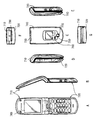
도 1은 본 개시된 한 실시의 형태에 관한 표시 장치의 구성을 도시하는 평면도 및 단면도.
도 2는 도 1에 도시한 표시 장치의 일부의 구성을 도시하는 단면도.
도 3은 도 1에 도시한 표시 영역 및 주변 영역의 구성도.
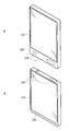
도 4의 A 및 B는 본 개시된 한 실시의 형태에 관한 표시 장치의 다른 예를 도시하는 평면도.
도 5의 A 및 B는 본 개시된 한 실시의 형태에 관한 표시 장치의 다른 예를 도시하는 평면도.
도 6의 A 및 B는 본 개시된 한 실시의 형태에 관한 표시 장치의 다른 예를 도시하는 평면도.
도 7의 A 및 B는 본 개시된 한 실시의 형태에 관한 표시 장치의 다른 예를 도시하는 평면도.
도 8의 A 및 B는 도 3에 도시한 화소 구동 회로의 한 예를 도시하는 도면.
도 9는 도 1에 도시된 표시 장치의 제조 방법의 플로우차트.
도 10의 A 내지 D는 도 1에 도시된 표시 장치의 제조 프로세스를 도시하는 도면.
도 11은 종래예 1의 표시 장치의 구성을 도시하는 평면도.
도 12는 종래예 2의 표시 장치의 구성을 도시하는 평면도.
도 13은 종래예 3의 표시 장치의 구성을 도시하는 평면도.
도 14의 A 및 B는 적용예 1의 외관을 도시하는 사시도.
도 15는 적용예 2의 외관을 도시하는 사시도.
도 16의 A는 적용예 3의 표측에서 본 외관을 도시하는 사시도, B는 이측에서 본 외관을 도시하는 사시도.
도 17은 적용예 4의 외관을 도시하는 사시도.
도 18은 적용예 5의 외관을 도시하는 사시도.
도 19의 A는 적용예 6의 연 상태의 정면도, B는 그 측단면, C는 닫은 상태의 정면도, D는 좌측면도, E는 우측면도, F는 상면도, G는 하면도.1 is a plan view and a cross-sectional view illustrating a configuration of a display device according to an embodiment of the present disclosure.
FIG. 2 is a cross-sectional view showing a configuration of a part of the display device shown in FIG. 1. FIG.
3 is a configuration diagram of a display area and a peripheral area shown in FIG. 1.
4A and 4B are plan views illustrating another example of the display device according to one embodiment of the present disclosure.
5A and 5B are plan views illustrating another example of the display device according to one embodiment of the present disclosure.
6A and 6B are plan views illustrating another example of the display device according to one embodiment of the present disclosure.
7 A and B are plan views illustrating another example of the display device according to one embodiment of the present disclosure.
8A and 8B illustrate an example of the pixel drive circuit shown in FIG. 3.
9 is a flowchart of a method of manufacturing the display device shown in FIG. 1.
10A to 10D illustrate a manufacturing process of the display device shown in FIG. 1.
11 is a plan view showing a configuration of a display device of a conventional example 1. FIG.
12 is a plan view illustrating a configuration of a display device of a conventional example 2. FIG.
FIG. 13 is a plan view showing a configuration of a display device of Conventional Example 3. FIG.
14: A and B are perspective views which show the external appearance of the application example 1. FIG.
15 is a perspective view illustrating an appearance of Application Example 2. FIG.
FIG. 16: A is a perspective view which shows the external appearance seen from the front side of the application example 3, B is a perspective view which shows the external appearance seen from the back side.
17 is a perspective view illustrating an appearance of Application Example 4. FIG.
18 is a perspective view illustrating an appearance of Application Example 5. FIG.
19A is a front view of the open state of Application Example 6, B is a side cross section thereof, C is a front view of a closed state, D is a left side view, E is a right side view, F is a top view, and G is a bottom view.
이하, 본 기술의 실시의 형태에 관해, 도면을 참조하여 상세히 설명한다. 또한, 설명은 이하의 순서로 행한다.EMBODIMENT OF THE INVENTION Hereinafter, embodiment of this technology is described in detail with reference to drawings. The description will be made in the following order.
1. 실시의 형태1. Embodiment
기판의 표면 및 이면에 형성되는 배선이 관통구멍을 통하여 전기적으로 접합된 표시 장치Display devices in which wirings formed on the front and rear surfaces of the substrate are electrically bonded through the through holes
(1-1) 전체 구성(1-1) Overall Configuration
(1-2) 제조 방법(1-2) Manufacturing Method
2. 적용예
2. Application Example
1. 실시의 형태1. Embodiment
(1-1) 전체 구성(1-1) Overall Configuration
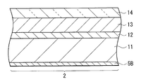
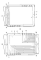
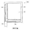
도 1은 본 개시된 한 실시의 형태에 관한 표시 장치(표시 장치(1))의 표면 및 이면의 평면 구성 및 단면 구성을 도시한 것이다. 도 1의 (A)는 표측(표시측)에서 본 평면 구성, 도 1의 (B)는 이측에서 본 평면 구성, 도 1의 (C)는 도 1의 (A)의 I-I'의 1점 쇄선을 따라 취해진 주변 영역(3)의 단면 구성을 각각 도시하고 있다. 이 표시 장치(1)는, 예를 들면, 유기 전계 발광(EL; Electro Luminescence) 현상을 이용하여 발광하는 유기 EL(electro luminescence) 텔레비전 장치, 또는 전기영동(電氣泳動) 현상을 이용하여 화상(예를 들면 문자 정보 등)을 표시하는 전기영동형 디스플레이(이른바 전자 페이퍼 디스플레이)이다. 표시 장치(1)의 표시 패널(10)은, 예를 들면, 기판(11) 상에, 복수의 화소(10A)(도 3 참조)가 매트릭스 형상으로 배치된 표시 영역(2)과, 주변 영역(3)에 의해 구성되어 있다. 주변 영역(3)에는, 표시 패널(10)의 외부에 마련된 영상 표시용의 드라이버인 신호선 구동 회로(7A) 및 주사선 구동 회로(7B)로부터 각 화소(10A)에의 구동 신호를 공급하는 배선(신호선(4)(제 3 배선) 및 주사선(5A)(제 1 배선))이 마련되어 있다. 그리고, 도 1의 (A) 내지 (C)는, 표시 장치(1)의 구조를 모식적으로 도시한 것이고, 실제의 치수 및 형상과는 다르다.1 illustrates a planar configuration and a cross-sectional configuration of the front and rear surfaces of a display device (display device 1) according to an embodiment of the present disclosure. Fig. 1A is a planar configuration seen from the front side (display side), Fig. 1B is a planar configuration viewed from the rear side, and Fig. 1C is 1 of I-I 'of Fig. 1A. The cross-sectional structure of the
도 2는, 표시 영역(2)의 일부의 단면 구성을 도시한 것이다. 도 2에 도시한 바와 같이, 표시 영역(2)은, 기판(11)상에 TFT층(12), 표시층(13) 및 투명 기판(14)이 이 순서로 적층된 구성을 갖고 있다. 도 3은, 표시 장치(1)의 개략 구성을 도시한 것이다.2 illustrates a cross-sectional configuration of a part of the
기판(11)(표시 기판)은, 예를 들면 사각형 형상이고, 그 윗면의 중앙부에 TFT층(12), 표시층(13) 및 투명 기판(14)이 이 순서로 적층된 영역이 표시 영역(2)이 된다. 한편, 기판(11)중, 표시 영역(2)을 둘러싸는 영역이 주변 영역(3)(피 표시 영역)이 된다. 기판(11)은 예를 들면, 유리, 석영, 실리콘, 갈륨비소 등의 무기 재료 또는, 폴리이미드, 폴리에틸렌테레프탈레이트(PET), 폴리에틸렌나프탈레이트(PEN), 폴리메틸메타크릴레이트(PMMA), 폴리카보네이트(PC), 폴리에테르술폰(PES), 폴리에틸에테르케톤(PEEK), 방향족 폴리에스테르(액정 폴리머) 등의 플라스틱 재료 등으로 이루어진다. 이 기판(11)은, 웨이퍼 등의 강성의 기판이라도 좋고, 박층 유리나 필름 등 가요성 기판이라도 좋다. 기판(11)이 가요성 기판이라면, 절곡 가능한 표시 장치를 실현할 수 있다.The board | substrate 11 (display board | substrate) is square shape, for example, and the area | region in which the
기판(11)에는, 직경 수십㎛ 정도의 관통구멍(11A)이 마련되어 있다. 이 관통구멍(11A)은, 표시층(12) 등이 영향을 받는 것을 막기 위해 주변 영역(3)에 마련하는 것이 바람직하다. 구체적으로는, 사각형 형상의 표시 패널(10)의 주변 영역(3)의 한 변, 예를 들면 후술하는 표면 배선(신호선(4) 및 주사선(5A))이 인출된 주변 영역(3)의 한 변에 마련된다. 관통구멍(11A)은 후술하는 표면 배선층 및 이면 배선층과 같은 재료에 의해 충전되고, 관통 전극(5C)을 형성하고 있다.The
TFT층(12)은, 복수의 디바이스를 포함하는 적층 구조를 가지며, 이 복수의 디바이스는, 박막(전극 등의 금속층이나, 절연막 등)을 포함하는 것이고, 상기한 바와 같이 기판(11)의 중앙부(표시 영역(2))에 배치되어 있다. 구체적으로는, 화소를 선택하기 위한 스위칭 소자로서의 트랜지스터(TFT ; Thin Film Transistor) 외에, 용량 소자(보존 용량 소자 등), 화소 구동 회로(도 3)가 되는 표면 배선층(신호선(4), 주사선(5A) 등) 및 전극(화소 전극 등) 등을 들 수 있다. 또한, TFT는, 채널층으로서 무기 반도체층을 이용한 무기 TFT 또는, 유기 반도체층을 이용한 유기 TFT의 어느 것에 의해 구성되어 있어도 좋다. 또한, 그 구성은, 예를 들면 역스태거 구조(이른바 보텀 게이트형)라도 좋고 스태거 구조(톱 게이트형)라도 좋고 특히 한정되지 않는다.The
또한, 기판(11)과 TFT층(12)과의 사이에는, TFT층(12) 및 표시층(13)에의 수분이나 유기 가스의 침입에 의한 열화를 방지하기 위해, 배리어층(도시 생략)을 마련하여도 좋다. 배리어층은, 예를 들면, 산화 실리콘(SiO2), 질화 실리콘(Si3N4), 산화 알루미늄(Al2O3), 질화 알루미늄(AlN), 산화 탄탈(Ta2O5) 또는 산화 질화 알루미늄(AlOxN1-x(단, X=0.01 내지 0.2))에 의해 형성된다.In addition, a barrier layer (not shown) is provided between the
표시층(13)은, 예를 들면 화소 전극과 공통 전극과의 사이에 유기 발광층을 갖는 유기 EL 소자이다. 화소 전극은 TFT층(12)에 화소마다 마련되고, 공통 전극은 표시층(13)상에 마련된 투명 기판(14)의 한 면에 걸쳐서 마련되어 있다. 또한, 표시층(13)은 유기 EL 소자로 한하지 않고, 발광층으로서 전기영동층을 갖는 전기영동 소자라도 좋다.The
투명 기판(14)에는 기판(11)과 같은 재료를 이용할 수 있다. 투명 기판(14)상에는, 또한 표시층(13)에의 수분의 침입을 방지하는 방습막 및 외광이 표시면에 비쳐 들어오는 것을 방지하기 위한 광학 기능막을 마련하도록 하여도 좋다.The same material as the
이면 배선층(제 2 배선)은, 화소 구동 회로의 일부이고, 기판(11)의 이면측에 마련되고, 기판(11)의 주변 영역(3)에 형성된 관통 전극(5C)을 통하여 TFT층(12) 내에 형성된 표면 배선과 전기적으로 접속되어 있다. 본 실시의 형태에서는, 이 이면 배선층은, 주사선(5)의 일부이고, 기판(11)의 표면에 마련된 주사선(5A)과 관통 전극(5C)을 통하여 접속된 주사선(5B)이다. 이 주사선(5B)은, 도 1의 (B)에 도시한 바와 같이, 기판(11)의 장축 방향으로 연재된 후, 소정의 위치에 단축 방향으로 굴곡하고, 기판(11)의 표면에 마련된 신호선(4)의 외부로의 취출 방향과 같은 방향으로 취출되어 있다.The back wiring layer (second wiring) is a part of the pixel driving circuit, is provided on the back surface side of the
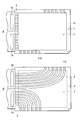
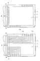
또한, 여기서는 주사선(5)을 기판(11)의 이면에 배치하였지만, 이것으로 한정되지 않고, 신호선을 이면측에 배치하여도 상관없다. 본 실시의 형태와 같이, 배선수가 적은 단변 방향(여기서는 주사선(5A))을 이면 배선에 의해 배치하는 경우에는, 게이트선이 적기 때문에 제조 공정이 용이해진다. 한편, 긴변 방향(여기서는 신호선(5))을 이면 배선에 의해 배치하는 경우에는, 신호선 구동 회로(7A) 및 주사선 구동 회로(7B) 등의 드라이버 IC나 드라이버 IC를 탑재하는 플렉시블 프린트 기판(FPC) 등을, 단변 방향에 형성한 배선 인출부에서 접속할 수 있다. 이 때문에, 배선 배치의 자유도가 향상한다. 또한, 기판(11)으로서 가요성 기판을 이용한 때에는, 드라이버 IC나 플렉시블 프린트 기판과의 접속부 등의 굴곡에 약한 부재를 단변 방향으로 집약할 수가 있어서, 표시 장치의 플렉시블성이 보다 향상한다. 또한, 본 실시의 형태에서는, 주사선(5B)을 소정의 위치에서 굴곡시켜서 배치하였지만, 이것으로 한정되지 않고, 예를 들면 도 4의 A, B에 도시한 바와 같이, 곡선형상으로 배치하여도 좋고, 도 5의 A, B에 도시한 바와 같이, 복수의 선분으로 이루어지는 라인 형상으로 배치하여도 좋다. 또한, 표면 배선 및 이면 배선은 각각 반드시 동일 변으로부터 취출할 필요는 없고, 예를 들면, 도 6의 A, B에 도시한 바와 같이, 이면 배선의 반수를 표면 배선과 동일 변으로부터 취출하고, 나머지 이면 배선을 표면 배선의 취출 변에 대향하는 변으로부터 취출하도록 하여도 좋다. 또한, 신호선(4A) 및 주사선(5A)은 반드시 동일 변으로부터 취출할 필요는 없고, 예를 들면 도 7의 A, B에 도시한 바와 같이, 서로 대향하는 변에서 취출하도록 하여도 좋다. 또한, 도 1, 도 4 내지 도 7에 도시한 바와 같이, 표면 배선 및 이면 배선을 동일 변 또는 서로 대향하는 변에서 취출함에 의해 가요성 기판을 이용하여 제작한 때의 표시 장치의 가요성을 향상하는 것이 가능해진다.In addition, although the
또한, 본 실시의 형태에서는, 표면 배선과 이면 배선을 관통구멍(11A)으로 이루어지는 접속부를 통하여 접속하였지만, 표면 배선과 이면 배선은 전기적으로 접속되어 있으면 되고, 관통구멍(11A) 외에, 예를 들면 표면 배선 및 이면 배선을 기판(11)의 단변(端邊)까지 마련하고, 기판(11)의 측면을 통하여 접속하도록 하여도 좋다. 단, 본 실시의 형태와 같이 관통구멍(11A)을 통하여 접속함에 의해, 접속부에서 단선 등의 부적합함의 발생을 막을 수 있다. 이 밖에, 별도 플렉시블 배선 기판을 이용하여 표면 배선과 이면 배선을 접속하는 접속부(도시 생략)를 마련하여도 좋다. 단, 본 실시의 형태와 같이 관통구멍(11A)을 통하여 접속함에 의해, 부품 갯수를 줄일 수 있다.In addition, in this embodiment, although the surface wiring and the back wiring were connected through the connection part which consists of 11 A of through-holes, the surface wiring and the back wiring should just be electrically connected, for example besides the through
또한, 상기 표면 배선층(신호선(4), 주사선(5A)), 이면 배선층(주사선(5B)) 및 관통 전극(5C)은, 일반적인 도전 재료, 예를 들면 몰리브덴(Mo), 크롬(Cr), 탄탈(Ta), 티탄(Ti), In 합금인 ITO나 IGO, IGZO 등의 투명 전극, 알루미늄(Al) 및 알루미늄 합금 등 중의 1종으로 이루어지는 단층막, 또는 2종 이상으로 이루어지는 적층막에 의해 구성되어 있다. 알루미늄 합금으로서는, 예를 들면 알루미늄-네오디뮴 합금을 들 수 있다.The surface wiring layer (
본 실시의 형태에서의 표시 장치(1)에서는, 화소 구동 회로는, 예를 들면 표시층(13)에 유기 EL 소자를 이용하는 경우에는, 도 8의 A에 도시한 바와 같이, 구동 트랜지스터(Tr1) 및 기록 트랜지스터(Tr2)와, 이들 트랜지스터(Tr1, Tr2)의 사이의 커패시터(보존 용량)(Cs)와, 제 1 전원 라인(Vcc) 및 제 2 전원 라인(GND)의 사이에서 구동 트랜지스터(Tr1)에 직렬로 접속된 각 화소를 구성하는 표시 소자를 갖는다. 또한, 표시층(13)에 전기영동 소자를 이용하는 경우에는, 도 8의 B에 도시한 바와 같은 화소 회로가 마련된다.In the
이 화소 구동 회로는, 예를 들면 도 3에 도시한 바와 같이, 열방향으로는 신호선(4)이 복수 배치되고, 행방향으로는 주사선(5A)이 복수 배치되어 있다. 각 신호선(4)과 각 주사선(5A)과의 교차점이 각 표시 소자에 대응하고 있다. 각 신호선(4)은, 플렉시블 프린트 기판(FPC)상에 마련된 신호선 구동 회로(7A)에 접속되고, 이 신호선 구동 회로(7A)로부터 신호선(4)을 통하여 기록 트랜지스터(Tr2)의 소스 전극에 화상 신호가 공급되도록 되어 있다. 각 주사선(5)은 신호선 구동 회로(7A)와 마찬가지로 FPC에 마련된 주사선 구동 회로(7B)에 접속되고, 이 주사선 구동 회로(7B)로부터 주사선(5)을 통하여 기록 트랜지스터(Tr2)의 게이트 전극에 주사 신호가 순차적으로 공급되도록 되어 있다.In this pixel drive circuit, for example, as shown in FIG. 3, a plurality of
본 실시의 형태의 주사선(5)에서는, 기판(11)의 표면에 마련된 주사선(5A)이 주변 영역(3)에 형성된 관통 전극(5C)을 통하여 기판(11)의 이면에 마련된 주사선(5B)에 접속되고, 신호선(4)과 동일 방향으로 취출되어 있다.In the
이 표시 장치(1)는, 예를 들면 이하와 같이 하여 제조할 수 있다. 또한, 여기서는 기판(11)으로서 가요성을 갖는 기판을 이용한 경우의 제조 공정을 설명한다.This
(1-2) 제조 방법(1-2) Manufacturing Method
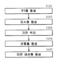
도 9는, 이 표시 장치(1)의 제조 방법의 흐름을 도시한 것이다. 우선, 도 10의 A에 도시한 바와 같이 기판(11)의 이면에 고정층(21)을 통하여 지지체(22)를 부착한 후, TFT층(12) 및 표시층(13)을 형성한다(스텝 S101, 102). 지지체(22)는, 기판(11)을 지지하는 것이고, 예를 들면 유리 기판이나 금속 기판을 이용할 수 있다. 고정층(21)은, 기판(11)을 지지체(22)에 고정하는 것이다. 이 고정층(21)은, 범용적인 점착제 및 점착 테이프를 이용할 수 있다. 구체적으로는, 예를 들면 아크릴계 접착제(점착제), 에폭시계 접착제, 실록산계 접착제, 우레탄계 접착제, 실란 커플링제, 천연고무계 접착제 또는 합성고무계 접착제 등을 들 수 있다. 이들 접착제는, 지지체(21)과 기판(11)과의 접촉면에, 스핀 코트법, 다이 코트 또는 그라비어 등의 인쇄법으로 도포함에 의해 형성한다. 또한, 점착 테이프를 이용하는 경우에는, 예를 들면 지지체(11)에 점착 테이프를 첨부하여 고정층(12)을 형성한 후, 라미네이터로 기판(13)을 고정한다.9 shows a flow of the manufacturing method of the
계속해서, 포토 리소그래피 등을 이용하여 TFT나 표면 배선층(신호선(4), 주사선(5A) 등) 등의 각종의 디바이스를 포함하는 TFT층(12)을 형성한다. 뒤이어, TFT층(12)상에, 예를 들면 TFT층(12)과 마찬가지로 포토 리소그래피 기술을 이용하여, 표시층(13)을 형성한다. 그 후, 이 표시층(13) 상에 공통 전극, 방습막 및 광학 기능막 등을 구비한 투명 기판(14)을 맞붙인다. 또한, 방습막 및 광학 기능막은, 공통 전극이 형성된 투명 기판(14)을 표시층(13)에 맞붙인 후, 투명 기판(14)상에 형성하여도 좋다.Subsequently, photolithography or the like is used to form a
다음에, 도 10의 B에 도시한 바와 같이 지지체(11)를 기판(13)으로부터 박리한다(스텝 S103). 지지체(21)와 기판(11)과의 분리 방법은, 예를 들면, 박리 시작부에 픽킹 테이프(picking tape)를 이용하여 박리하여도 좋다. 또한, 고정층(12)은 지지체(11)에 부착한 상태라도 좋지만, 필요에 응하여 제거하여도 좋다.Next, as shown in FIG. 10B, the
계속해서, 도 10의 C에 도시한 바와 같이 기판(11)을 반전하여 이면측을 윗면으로 하고 관통구멍(11A)을 형성한다(스텝 S104). 관통구멍(11A)의 형성 방법으로서는, 구체적으로는, CO2 레이저에 의한 가공, 천공 가공기를 이용한 가공을 들 수 있다. 또한, 기판(11)을 용해하는 용제를 잉크젯법이나 디스펜서에 의해 국소적으로 도포함으로써 관통구멍(11A)을 형성하여도 좋다. 또한, 여기서는 기판(11)의 이면측을 윗면으로 하여 관통구멍(11A)을 형성하였지만, 이면 가공을 할 수 있으면 반드시 기판(11)을 반전할 필요는 없다.Subsequently, as shown in FIG. 10C, the
다음에, 도 10의 D에 도시한 바와 같이 기판(11)의 이면에 이면 배선층(주사선(5B))을 형성한다(스텝 S105). 이면 배선층의 형성 방법으로서는, 예를 들면 잉크젯 방식, 스핀 코트 방식, 슬릿 코트 방식, 스크린 인쇄 방식, 오프셋 인쇄 방식, 플렉소 인쇄 방식, 그라비어 인쇄 방식 또는 철판(凸版) 인쇄 방식 등의 각종 인쇄 방식 외에, 스프레이 코트 등을 이용할 수 있다. 또한, 배선폭과 배선 사이의 간격은, 예를 들면 L/S=30㎛/30㎛ 내지 20㎛/20㎛이면 충분한다.Next, as shown in FIG. 10D, a backside wiring layer (scanning
최후로, 기판(11)의 표면의 긴변 방향으로 취출된 신호선(4) 및 마찬가지로 이면의 긴변 방향으로 취출된 주사선(5B)에 각각 신호선 구동 회로(7A) 및 주사선 구동 회로(7B)를 구비한 FPC를, 배선 인출부에서, 예를 들면 열압착에 의해 전기적으로 접속시킨다. 이에 의해 표시 장치(1)가 완성된다. 또한, 이들의 구동 회로는, FPC를 통하여 접속되지 않아도, 긴변 방향에 마련된 칩위에 탑재하고, 배선 인출부에서 전기적으로 접속되어 있어도 좋다.Finally, a signal
이 표시 장치(1)에서는, 각 화소(10A)에 대해 주사선 구동 회로(7B)로부터 기록 트랜지스터(Tr2)의 게이트 전극을 통하여 주사 신호가 공급됨과 함께, 신호선 구동 회로(7A)로부터 화상 신호가 기록 트랜지스터(Tr2)를 통하여 보존 용량(Cs)에 유지된다. 즉, 이 보존 용량(Cs)에 유지된 신호에 응하여 구동 트랜지스터(Tr1)가 온 오프 제어되고, 이에 의해, 표시 소자의 구동이 제어된다.In the
본 실시의 형태의 표시 장치(1)에서는, 기판(11)의 이면에 이면 배선을 형성하고, 이 이면 배선과, 기판(11)의 표면에 마련된 화소 구동 회로를 구성하는 배선(여기서는 주사선(5A))을 전기적으로 접속함에 의해, 배선의 취출 방향을 일방향으로 정리하는 것이 가능해진다. 이에 의해, 배선 설계의 자유도가 향상하고, 주변 영역(3)에 마련되는 배선 패턴을 간소화하는 것이 가능해진다. 즉, 협 액자화가 가능해짐과 함께, 가요성을 갖는 기판을 이용한 표시 장치에서는, 모듈 전체의 가요성(flexibility)을 실현할 수 있다. 이하, 이에 관해 더 설명한다.In the
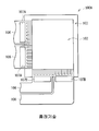
도 11은, 종래의 디스플레이 모듈(표시 장치(100A))의 평면 구성을 도시한 것이다. 이 표시 장치(100A)에서는, 표시 영역(102)에서 행방향 및 열방향으로 복수 배치된 배선(신호선(4) 및 주사선(5))은, 그대로 같은 방향으로 연재되고, 사각형 형상의 기판(111)의 2방향으로부터 외부에 취출된다. 이들 신호선(104) 및 주사선(105)은, 각각 신호선 구동 회로(107A)나 주사선 구동 회로(107B) 등의 드라이버 IC가 탑재된 FPC에 접속되어 있다. 이와 같은 표시 장치(100A)에서는, 기판(111)으로서 가요성 기판을 이용하여도, 사각형 형상의 기판(11)의 2변에 접속된 드라이버 IC나 FPC에 의해, 모듈의 가요성이 저해된다는 문제가 있다.11 shows a planar configuration of a conventional display module (
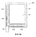
이 문제를 해결하기 위해, 전술한 바와 같이 도 12 및 도 13에 도시한 표시 장치(100B, 100C)가 보고되어 있다. 이 표시 장치(100B)는, 기판(111)의 주변 영역(103)에 신호선 구동 회로(107A)나 주사선 구동 회로(107B) 등의 드라이버 IC를 직접 실장(칩 실장)한 것이고, 이에 의해, 취출 배선수를 줄일 수 있다. 또한, 표시 장치(100C)는, 통상 표시 영역(102) 내에 형성되는 TFT의 구동 드라이버(108)(내장 회로)를 기판(11)의 주변 영역(103)에 형성한 것이고, 표시 장치(100B)와 마찬가지로 취출 배선수를 줄일 수 있다. 이에 의해, 표시 패널 외부에의 배선의 추출 위치는 1곳에 집약되고, 드라이버(IC107A, 107B)나 FPC(106)에 의한 모듈의 가요성의 저해는 저감된다. 그러나, 이와 같은 구성의 표시 장치(100B, 100C)에서는, 기판(111)상에 실장된 드라이버(IC107A, 107B)나 구동 드라이버(108)로부터 외부에 인출하는 배선을 주변 영역(103)에 형성할 필요가 있다. 이 때문에, 적어도 드라이버 IC나 구동 드라이버가 마련된 측의 주변 영역(103)을 넓게 할 필요가 있고, 액자 영역(주변 영역(103))이 넓게 된다는 문제가 생긴다. 또한, 표시 패널 내에서의 표시 영역(102)의 위치가 치우쳐서, 디스플레이로서의 디자인성이 저하된다는 문제도 발생한다. 또한, 일반적으로 칩 실장은, 솔더 부착에 의해 행하여지는데, 솔더 부착은 200℃ 이상의 가열이 필수이기 때문에, 기판(111)으로서 플라스틱 등의 가요성 기판을 이용한 경우에는, 기판의 용해나 변형 등이 발생한다. 또한, 표시 장치(100C)와 같이, 기판(111)상에 TFT를 포함하는 드라이버를 혼재한 경우에는 높은 TFT 이동도가 필요해진다. 채널로서 폴리실리콘 등을 이용하는 무기 TFT에서는, 그 이동도는 수10 내지 수100㎠/Vs 정도로 높기 때문에 문제 없지만, 유기 TFT의 이동도는 현재의 상태에서 1㎠/Vs 정도여서이고, 이동도가 부족하고 있다. 이와 같이, 도 12나 도 13에 도시한 표시 장치(100B, 100C)에서는, 표시 장치로서 이용 가능한 재료가 한정되고, 특히, 가요성을 갖는 모듈에 적용하는 것은 곤란하였었다.In order to solve this problem, the
이에 대해, 본 실시의 형태의 표시 장치(1)에서는, 기판(11)의 표면측에 형성된 신호선(4) 및 주사선(5) 등의 화소 구동 회로 중, 한쪽을 기판(11)의 이면측에 배치하였다. 이에 의해, 주변 영역(3)에 형성되는 배선 설계의 자유도가 향상한다.In contrast, in the
이상과 같이 본 실시의 형태의 표시 장치(1)에서는, 기판(11)의 이면에 배선을 마련하고, 이 이면 배선과 표면에 마련된 배선을 전기적으로 접속하도록 하였기 때문에, 주변 영역(3)에 형성되는 배선의 설계 자유도가 향상하고, 배선의 외부로의 인출을 일방향으로부터 행하는 것이 가능해진다. 이에 의해, 이 표시 장치(1)를, 가요성 기판을 이용하여 제작한 경우에는, 표시 장치(1) 전체의 보다 높은 가요성이 실현된다. 또한, 표시 영역(2)의 배선을 간소화하는 것이 가능해지기 때문에, 표시 장치(1)의 협액자화가 가능하게 된다.As described above, in the
상기 표시 장치(1)는, 예를 들면 다음의 적용예 1 내지 6에 나타낸 전자 기기에 탑재할 수 있다.The
(적용예 1)(Application Example 1)
도 14의 A 및 B는, 전자 북의 외관을 도시한 것이다. 이 전자 북은, 예를 들면, 표시 영역(210), 비표시 영역(220) 및 조작부(230)를 갖고 있다. 조작부(230)는, 도 10의 A에 도시한 바와 같이 표시 영역(210)과 같은 면(앞면)에 형성되어 있어도, 도 14의 B에 도시한 바와 같이 표시 영역(210)과는 다른 면(윗면)에 형성되어 있어도 좋다.14A and 14B show the appearance of the electronic book. This electronic book has the
(적용예 2)(Application Example 2)
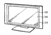
도 15는, 텔레비전 장치의 외관을 도시한 것이다. 이 텔레비전 장치는, 예를 들면, 프런트 패널(310) 및 필터 유리(320)를 포함하는 영상 표시 화면부(300)를 갖고 있다.Fig. 15 shows the appearance of a television device. This television apparatus has the video
(적용예 3)(Application Example 3)
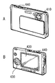
도 16은, 디지털 스틸 카메라의 외관을 도시한 것이다. 이 디지털 스틸 카메라는, 예를 들면, 플래시용의 발광부(410), 표시 영역(420), 메뉴 스위치(430) 및 셔터 버튼(440)을 갖고 있다.16 shows the appearance of a digital still camera. This digital still camera has, for example, a
(적용예 4)(Application Example 4)
도 17은, 노트형 퍼스널 컴퓨터의 외관을 도시한 것이다. 이 노트형 퍼스널 컴퓨터는, 예를 들면, 본체(510), 문자 등의 입력 조작을 위한 키보드(520) 및 화상을 표시하는 표시 영역(530)을 갖고 있다.Fig. 17 shows the appearance of a notebook personal computer. This notebook personal computer has a
(적용예 5)(Application Example 5)
도 18은, 비디오 카메라의 외관을 도시한 것이다. 이 비디오 카메라는, 예를 들면, 본체부(610), 이 본체부(610)의 전방 측면에 마련된 피사체 촬영용의 렌즈(620), 촬영시의 스타트/스톱 스위치(630) 및 표시 영역(640)을 갖고 있다.18 shows the appearance of a video camera. The video camera includes, for example, a
(적용예 6)(Application Example 6)
도 19는, 휴대 전화기의 외관을 도시한 것이다. 이 휴대 전화기는, 예를 들면, 상측 몸체(710)와 하측 몸체(720)를 연결부(힌지부)(730)로 연결한 것이고, 디스플레이(740), 서브 디스플레이(750), 픽처 라이트(760) 및 카메라(770)를 갖고 있다.19 shows the appearance of a mobile phone. The mobile phone is, for example, the
이상, 실시의 형태 및 변형례를 들어서 본 기술을 설명하였지만, 본 기술은 상기 실시의 형태 등으로 한정되는 것이 아니고, 여러가지 변형이 가능하다. 예를 들면, 상기 실시의 형태 등에서는, 표시층(12)을 전기영동형의 표시체에 의해 구성한 경우에 관해 설명하였지만, 표시층(12)은, 액정, 유기 EL(Electroluminescence) 또는 무기 EL 등에 의해 구성되어 있어도 좋다.As mentioned above, although this embodiment was described with reference to embodiment and a modification, this technology is not limited to the said embodiment etc., A various deformation | transformation is possible. For example, in the above embodiment and the like, the case where the
또한, 도 1에서는, 관통구멍(11A)의 지름의 크기가 표면측과 이면측에서 동일 지름으로 되어 있는 것을 예시하였지만, 표면측과 이면측에서 달라도 좋고, 복수의 관통구멍(11A)의 지름이 전부 동일하여도, 달라도 좋다.In addition, in FIG. 1, although the magnitude | size of the diameter of the through
또한, 상기 실시의 형태 등에서 설명한 각 층의 재료 및 두께, 또는 성막 방법 및 성막 조건 등은 한정되는 것이 아니고, 다른 재료 및 두께로 하여도 좋고, 또는 다른 성막 방법 및 성막 조건으로 하여도 좋다.In addition, the material and thickness of each layer demonstrated in the said embodiment etc., a film-forming method, film-forming conditions, etc. are not limited, It may be made of another material and thickness, or may be made into another film-forming method and film-forming conditions.
또한, 상기 실시의 형태 등에서는, 표시 장치(1)의 구성을 구체적으로 들어서 설명하였지만, 모든 층을 구비할 필요는 없고, 또한, 다른 층을 더욱 구비하고 있어도 좋다.In addition, although the structure of the
또한, 본 기술은 이하와 같은 구성도 취할 수 있다.The present technology can also take the following configuration.
(1) 표시 영역 및 주변 영역이 마련된 기판과, 상기 기판의 표면에 마련된 제 1 배선과, 상기 기판의 이면에 마련됨과 함께, 상기 제 1 배선과 전기적으로 접속된 제 2 배선을 구비한 표시 장치.(1) A display device comprising a substrate provided with a display region and a peripheral region, a first wiring provided on the surface of the substrate, and a second wiring provided on the back surface of the substrate and electrically connected to the first wiring. .
(2) 상기 제 1 배선과 제 2 배선은, 상기 기판의 주변 영역에 마련된 접속부를 통하여 접속되어 있는, 상기 (1)에 기재된 표시 장치.(2) The display device according to (1), wherein the first wiring and the second wiring are connected via a connecting portion provided in a peripheral region of the substrate.
(3) 상기 접속부는 1 또는 2 이상의 관통구멍인, 상기 (2)에 기재된 표시 장치.(3) The display device according to (2), wherein the connection portion is one or two or more through holes.
(4) 상기 제 1 배선은 상기 표시 영역에 접속된 복수의 배선으로 이루어지고, 상기 제 2 배선은 각각 상기 제 1 배선에 전기적으로 접속된 복수의 배선으로 이루어지는, 상기 (1) 내지 (3)의 어느 하나에 기재된 표시 장치.(4) The said (1)-(3) said 1st wiring consists of a some wiring connected to the said display area, and the said 2nd wiring consists of a some wiring electrically connected to the said 1st wiring, respectively. The display device according to any one of.
(5) 상기 기판은 사각형 형상을 가지며, 상기 제 1 배선은 상기 기판의 적어도 한 변을 따라서 마련된 관통구멍을 통하여 상기 제 2 배선에 접속되어 있는, 상기 (1) 내지 (4)의 어느 하나에 기재된 표시 장치.(5) The substrate has a quadrangular shape, and the first wiring is connected to any one of (1) to (4) connected to the second wiring through a through hole provided along at least one side of the substrate. The display device described.
(6) 상기 제 1 배선은, 상기 기판의 표면에서 상기 표시 영역에 접속되고, 상기 제 2 배선은, 일단이 상기 기판의 한 변에서 상기 접속부를 통하여 상기 제 1 배선과 전기적으로 접속됨과 함께, 타단이 상기 기판의 다른 변에 마련된 배선 인출부까지 마련되어 있는, 상기 (1) 내지 (5)의 어느 하나에 기재된 표시 장치.(6) The said 1st wiring is connected to the said display area from the surface of the said board | substrate, The said 2nd wiring is electrically connected with the said 1st wiring through the said connection part in the one side of the said board | substrate, The display device according to any one of (1) to (5), wherein the other end is provided to a wiring lead portion provided on the other side of the substrate.
(7) 상기 표시 영역은, 행형상으로 마련된 복수의 신호선과, 열형상으로 마련된 복수의 주사선과, 상기 신호선과 주사선과의 교점에 마련된 화소를 가지며, 상기 제 1 배선은 상기 신호선 또는 상기 주사선의 한쪽에 접속되어 있는, 상기 (1) 내지 (6)의 어느 하나에 기재된 표시 장치.(7) The display area includes a plurality of signal lines arranged in a row shape, a plurality of scanning lines arranged in a column shape, and pixels provided at intersections of the signal lines and the scanning lines, and the first wiring line includes the signal lines or the scanning lines. The display device in any one of said (1)-(6) connected to one.
(8) 상기 신호선은 신호선 구동 회로에 전기적으로 접속되고, 상기 주사선은 주사선 구동 회로에 전적으로 접속되어 있는, 상기 (7)에 기재된 표시 장치.(8) The display device according to (7), wherein the signal line is electrically connected to a signal line driver circuit, and the scan line is entirely connected to a scan line driver circuit.
(9) 상기 신호선 또는 상기 주사선의 한쪽은 상기 제 1 배선, 상기 접속부 및 상기 제 2 배선을 통하여 상기 배선 인출부에 접속되고, 상기 배선 인출부는 상기 신호선 구동 회로 또는 상기 주사선 구동 회로에 전기적으로 접속되어 있는, 상기 (8)에 기재된 표시 장치.(9) One of the signal line or the scanning line is connected to the wiring lead-out portion through the first wiring, the connecting portion, and the second wiring, and the wiring lead-out portion is electrically connected to the signal line driving circuit or the scanning line driving circuit. The display device as described in said (8).
(10) 상기 신호선 구동 회로 및 상기 주사선 구동 회로는, 상기 사각형 형상을 갖는 기판의 동일 변에 마련되어 있는, 상기 (8) 또는 (9)에 기재된 표시 장치.(10) The display device according to (8) or (9), wherein the signal line driver circuit and the scan line driver circuit are provided on the same side of the substrate having the rectangular shape.
(11) 상기 신호선 구동 회로 및 상기 주사선 구동 회로는, 상기 사각형 형상을 갖는 기판의 상기 배선 인출부가 마련된 다른 변에 마련되어 있는, 상기 (8) 내지 (10)의 어느 하나에 기재된 표시 장치.(11) The display device according to any one of (8) to (10), wherein the signal line driver circuit and the scan line driver circuit are provided on the other side provided with the wiring lead portion of the substrate having the rectangular shape.
(12) 상기 신호선 구동 회로 및 상기 주사선 구동 회로는, 상기 사각형 형상을 갖는 기판의 대향하는 변에 각각 마련되어 있는, 상기 (8) 내지 (11)의 어느 하나에 기재된 표시 장치.(12) The display device according to any one of (8) to (11), wherein the signal line driver circuit and the scan line driver circuit are provided on opposite sides of the substrate having the rectangular shape.
(13) 상기 신호선 구동 회로 및 상기 주사선 구동 회로는, 한쪽이 상기 사각형 형상을 갖는 기판의 상기 인출부가 마련된 다른 변에 마련됨과 함께, 다른쪽이 상기 다른 변과 대향하는 변에 마련되어 있는, 상기 (8) 내지 (12)의 어느 하나에 기재된 표시 장치.(13) Said signal line driver circuit and said scanning line driver circuit are provided in the other side by which the said lead-out part of the board | substrate which has the said square shape was provided, and the other side is provided in the side which opposes the said other side. The display device according to any one of 8) to (12).
(14) 상기 신호선 구동 회로 및 상기 주사선 구동 회로는 구동 회로 기판상에 마련되어 있는, 상기 (8) 내지 (13)의 어느 하나에 기재된 표시 장치.(14) The display device according to any one of (8) to (13), wherein the signal line driver circuit and the scan line driver circuit are provided on a driver circuit board.
(15) 상기 구동 회로 기판은, 플렉시블 프린트 기판인, 상기 (14)에 기재된 표시 장치.(15) The display device according to (14), wherein the drive circuit board is a flexible printed board.
(16) 상기 기판의 표면에 상기 제 1 배선과는 다른 층에 배설된 제 3 배선을 가지며, 상기 제 3 배선 및 상기 제 2 배선은, 상기 관통구멍이 마련된 상기 기판의 한 변과는 다른 한 변으로부터 취출되어 있는, 상기 (5) 내지 (15)의 어느 하나에 기재된 표시 장치.(16) It has a 3rd wiring arrange | positioned in the layer different from the said 1st wiring on the surface of the said board | substrate, and the said 3rd wiring and the said 2nd wiring are different from the one side of the said board | substrate with which the said through hole was provided. The display device according to any one of (5) to (15), taken out from the side.
(17) 상기 기판은 가요성 기판인, 상기 (1) 내지 (16)의 어느 하나에 기재된 표시 장치.(17) The display device according to any one of (1) to (16), wherein the substrate is a flexible substrate.
(18) 상기 가요성 기판은 사각형 형상을 가지며, 한 변의 방향에 대한 가요성이 다른 변의 방향에 대한 가요성보다도 높은, 상기 (17)에 기재된 표시 장치.(18) The display device according to (17), wherein the flexible substrate has a rectangular shape, and the flexibility with respect to the direction of one side is higher than the flexibility with respect to the direction of the other side.
(19) 표시 장치를 구비하고, 상기 표시 장치는, 표시 영역 및 주변 영역이 마련된 기판과, 상기 기판의 표면에 마련된 제 1 배선과, 상기 기판의 이면에 마련됨과 함께, 상기 제 1 배선과 전기적으로 접속된 제 2 배선을 갖는 전자 기기.(19) A display device is provided, wherein the display device includes a substrate provided with a display region and a peripheral region, a first wiring provided on a surface of the substrate, and a rear surface of the substrate, and is electrically connected with the first wiring. An electronic device having a second wiring connected by a wire.
본 발명은 2011년 8월 11일자로 일본특허청에 특허출원된 일본특허원 제2011-175832호를 우선권으로 주장한다.The present invention claims priority to Japanese Patent Application No. 2011-175832 filed with the Japan Patent Office on August 11, 2011.
당업자라면, 하기의 특허청구범위 또는 그 등가의 범위 내에서, 설계상의 필요 또는 다른 요인에 따라, 상기 실시의 형태에 대한 여러 가지 변형예, 조합예, 부분 조합예, 및 수정예를 실시할 수 있을 것이다.Those skilled in the art can carry out various modifications, combinations, partial combinations, and modifications to the above embodiments, depending on design needs or other factors, within the scope of the following claims or equivalents thereof. There will be.
1, 100A, 100B, 100C : 표시 장치 2 : 표시 영역
3 : 주변 영역 4 : 신호선
5(5A, 5B, 5C) : 주사선 6 : FPC
7A : 신호선 구동 회로 7B : 주사선 구동 회로
10 : 표시 패널 11 : 기판
11A : 관통구멍 12 : TFT층
13 : 표시층 14 : 투명 기판
21 : 고정층 22 : 지지체1, 100A, 100B, 100C: display device 2: display area
3: peripheral area 4: signal line
5 (5A, 5B, 5C): Scanning line 6: FPC
7A: signal
10
11A: through hole 12: TFT layer
13: display layer 14: transparent substrate
21: fixed layer 22: support
Claims (19)
상기 기판의 표면에 마련된 제 1 배선; 및
상기 기판의 이면에 마련됨과 함께, 상기 제 1 배선과 전기적으로 접속된 제 2 배선을 포함하는 것을 특징으로 하는 표시 장치.A substrate provided with a display area and a peripheral area;
First wiring provided on a surface of the substrate; And
And a second wiring provided on the back surface of the substrate and electrically connected to the first wiring.
상기 제 1 배선과 제 2 배선은, 상기 기판의 주변 영역에 마련된 접속부를 통하여 접속되어 있는 것을 특징으로 하는 표시 장치.The method of claim 1,
The first wiring and the second wiring are connected via a connecting portion provided in a peripheral region of the substrate.
상기 접속부는 1 또는 2 이상의 관통구멍인 것을 특징으로 하는 표시 장치.The method of claim 2,
And the connection portion is one or two or more through holes.
상기 제 1 배선은 상기 표시 영역에 접속된 복수의 배선으로 이루어지고, 상기 제 2 배선은 각각 상기 제 1 배선에 전기적으로 접속된 복수의 배선으로 이루어지는 것을 특징으로 하는 표시 장치.The method of claim 1,
And said first wiring is made up of a plurality of wirings connected to said display area, and said second wiring is made up of a plurality of wirings electrically connected to said first wirings, respectively.
상기 기판은 사각형 형상을 가지며, 상기 제 1 배선은 상기 기판의 적어도 한 변을 따라서 마련된 관통구멍을 통하여 상기 제 2 배선에 접속되어 있는 것을 특징으로 하는 표시 장치.The method of claim 1,
The substrate has a rectangular shape, and the first wiring is connected to the second wiring through a through hole provided along at least one side of the substrate.
상기 제 1 배선은, 상기 기판의 표면에서 상기 표시 영역에 접속되고, 상기 제 2 배선은, 일단이 상기 기판의 한 변에서 상기 접속부를 통하여 상기 제 1 배선과 전기적으로 접속됨과 함께, 타단이 상기 기판의 다른 변에 마련된 배선 인출부까지 배설되어 있는 것을 특징으로 하는 표시 장치.The method of claim 1,
The first wiring is connected to the display area on the surface of the substrate, and the second wiring has one end electrically connected to the first wiring through the connection portion at one side of the substrate, and the other end is connected to the display region. The display apparatus is arrange | positioned even the wiring lead-out part provided in the other side of a board | substrate.
상기 표시 영역은, 행형상으로 마련된 복수의 신호선과, 열형상으로 마련된 복수의 주사선과, 상기 신호선과 주사선과의 교점에 마련된 화소를 가지며, 상기 제 1 배선은 상기 신호선 또는 상기 주사선의 한쪽에 접속되어 있는 것을 특징으로 하는 표시 장치.The method of claim 1,
The display area has a plurality of signal lines arranged in a row shape, a plurality of scanning lines arranged in a column shape, and pixels provided at intersections of the signal lines and the scanning lines, and the first wiring is connected to either the signal line or the scanning line. The display device characterized by the above-mentioned.
상기 신호선은 신호선 구동 회로에 전기적으로 접속되고, 상기 주사선은 주사선 구동 회로에 전적으로 접속되어 있는 것을 특징으로 하는 표시 장치.8. The method of claim 7,
And the signal line is electrically connected to the signal line driver circuit, and the scan line is entirely connected to the scan line driver circuit.
상기 신호선 또는 상기 주사선의 한쪽은 상기 제 1 배선, 상기 접속부 및 상기 제 2 배선을 통하여 상기 배선 인출부에 접속되고, 상기 배선 인출부는 상기 신호선 구동 회로 또는 상기 주사선 구동 회로에 전기적으로 접속되어 있는 것을 특징으로 하는 표시 장치.The method of claim 8,
One of the signal line or the scanning line is connected to the wiring lead-out part through the first wiring, the connecting portion, and the second wiring, and the wiring lead-out portion is electrically connected to the signal line driving circuit or the scanning line driving circuit. Display device characterized in that.
상기 신호선 구동 회로 및 상기 주사선 구동 회로는, 상기 사각형 형상을 갖는 기판의 동일 변에 마련되어 있는 것을 특징으로 하는 표시 장치.The method of claim 8,
The signal line driver circuit and the scan line driver circuit are provided on the same side of the substrate having the rectangular shape.
상기 신호선 구동 회로 및 상기 주사선 구동 회로는, 상기 사각형 형상을 갖는 기판의 상기 배선 인출부가 마련된 다른 변에 마련되어 있는 것을 특징으로 하는 표시 장치.The method of claim 8,
The signal line driver circuit and the scan line driver circuit are provided on different sides of the wiring lead portion of the substrate having the rectangular shape.
상기 신호선 구동 회로 및 상기 주사선 구동 회로는, 상기 사각형 형상을 갖는 기판의 대향하는 변에 각각 마련되어 있는 것을 특징으로 하는 표시 장치.The method of claim 8,
The signal line driver circuit and the scan line driver circuit are provided on opposite sides of the substrate having the rectangular shape, respectively.
상기 신호선 구동 회로 및 상기 주사선 구동 회로는, 한쪽이 상기 사각형 형상을 갖는 기판의 상기 인출부가 마련된 다른 변에 마련됨과 함께, 다른쪽이 상기 다른 변과 대향하는 변에 마련되어 있는 것을 특징으로 하는 표시 장치.The method of claim 8,
The signal line driver circuit and the scan line driver circuit are provided on the other side of which the lead-out portion of the substrate having one of the quadrangular shapes is provided, and on the other side of the signal line driver circuit and the scan line driver circuit. .
상기 신호선 구동 회로 및 상기 주사선 구동 회로는 구동 회로 기판상에 마련되어 있는 것을 특징으로 하는 표시 장치.The method of claim 8,
And the signal line driver circuit and the scan line driver circuit are provided on a driver circuit board.
상기 구동 회로 기판은, 플렉시블 프린트 기판인 것을 특징으로 하는 표시 장치.The method of claim 14,
The drive circuit board is a flexible printed circuit board.
상기 기판의 표면에 상기 제 1 배선과는 다른 층에 마련된 제 3 배선을 더 포함하며,
상기 제 3 배선 및 상기 제 2 배선은, 상기 관통구멍이 마련된 상기 기판의 한 변과는 다른 한 변으로부터 취출되어 있는 것을 특징으로 하는 표시 장치.6. The method of claim 5,
A third wiring provided on a surface different from the first wiring on the surface of the substrate,
The third wiring and the second wiring are taken out from one side different from one side of the substrate on which the through hole is provided.
상기 기판은 가요성 기판인 것을 특징으로 하는 표시 장치.The method of claim 1,
And the substrate is a flexible substrate.
상기 가요성 기판은 사각형 형상을 가지며, 한 변의 방향에 대한 가요성이 다른 변의 방향에 대한 가요성보다도 높은 것을 특징으로 하는 표시 장치.18. The method of claim 17,
The flexible substrate has a rectangular shape, and the flexibility of the direction of one side is higher than the flexibility of the direction of the other side.
상기 표시 장치는:
표시 영역 및 주변 영역이 마련된 기판과;
상기 기판의 표면에 마련된 제 1 배선과;
상기 기판의 이면에 마련됨과 함께, 상기 제 1 배선과 전기적으로 접속된 제 2 배선을 포함하는 것을 특징으로 하는 전자 기기.Includes a display device,
The display device is:
A substrate provided with a display area and a peripheral area;
First wiring provided on a surface of the substrate;
And a second wiring provided on the back surface of the substrate and electrically connected to the first wiring.
Applications Claiming Priority (2)
| Application Number | Priority Date | Filing Date | Title |
|---|---|---|---|
| JPJP-P-2011-175832 | 2011-08-11 | ||
| JP2011175832A JP2013040981A (en) | 2011-08-11 | 2011-08-11 | Display device and electronic apparatus |
Publications (1)
| Publication Number | Publication Date |
|---|---|
| KR20130018126A true KR20130018126A (en) | 2013-02-20 |
Family
ID=47677242
Family Applications (1)
| Application Number | Title | Priority Date | Filing Date |
|---|---|---|---|
| KR1020120084244A KR20130018126A (en) | 2011-08-11 | 2012-08-01 | Display device and electronic unit |
Country Status (5)
| Country | Link |
|---|---|
| US (2) | US9097945B2 (en) |
| JP (1) | JP2013040981A (en) |
| KR (1) | KR20130018126A (en) |
| CN (2) | CN102956156B (en) |
| TW (1) | TWI470594B (en) |
Cited By (1)
| Publication number | Priority date | Publication date | Assignee | Title |
|---|---|---|---|---|
| KR20170081076A (en) * | 2015-12-31 | 2017-07-11 | 엘지디스플레이 주식회사 | Flexible display device |
Families Citing this family (8)
| Publication number | Priority date | Publication date | Assignee | Title |
|---|---|---|---|---|
| JP2013040981A (en) * | 2011-08-11 | 2013-02-28 | Sony Corp | Display device and electronic apparatus |
| CN202816322U (en) * | 2012-09-19 | 2013-03-20 | 深圳市柔宇科技有限公司 | Display screen |
| TWI464731B (en) * | 2012-09-20 | 2014-12-11 | Au Optronics Corp | Display-driving structure and signal transmission method thereof, displaying device and manufacturing method thereof |
| KR20170059523A (en) * | 2015-11-20 | 2017-05-31 | 삼성디스플레이 주식회사 | Display apparatus, tiled display apparatus and method of manufacturing the same |
| CN106653819B (en) | 2017-02-17 | 2020-02-14 | 京东方科技集团股份有限公司 | Array substrate and display device |
| CN109390351B (en) * | 2017-08-02 | 2021-01-22 | 京东方科技集团股份有限公司 | Wiring structure and preparation method thereof, OLED array substrate, and display device |
| CN109786391B (en) | 2017-11-10 | 2021-08-03 | 京东方科技集团股份有限公司 | Array substrate, manufacturing method thereof, and display device |
| KR20210107189A (en) | 2020-02-21 | 2021-09-01 | 삼성디스플레이 주식회사 | Display device |
Family Cites Families (18)
| Publication number | Priority date | Publication date | Assignee | Title |
|---|---|---|---|---|
| JPH06148671A (en) * | 1992-11-13 | 1994-05-27 | Sharp Corp | Mounting structure for panel |
| JP3915380B2 (en) * | 2000-07-31 | 2007-05-16 | セイコーエプソン株式会社 | Liquid crystal device and electronic device |
| JP2002214634A (en) * | 2001-01-17 | 2002-07-31 | Matsushita Electric Ind Co Ltd | Transparent resin substrate for display element and liquid crystal display panel using the same |
| WO2002079867A1 (en) * | 2001-03-29 | 2002-10-10 | Koninklijke Philips Electronics N.V. | Display device and method of manufacturing the same |
| JP4156861B2 (en) * | 2002-05-07 | 2008-09-24 | ローム株式会社 | Organic EL display device and portable terminal |
| JP4059731B2 (en) * | 2002-08-19 | 2008-03-12 | シャープ株式会社 | Active matrix substrate and display device |
| US7557779B2 (en) * | 2003-06-13 | 2009-07-07 | Semiconductor Energy Laboratory Co., Ltd. | Display device |
| JP4032353B2 (en) * | 2003-12-26 | 2008-01-16 | セイコーエプソン株式会社 | Circuit board manufacturing method, circuit board, electronic device, and electro-optical device |
| JP2006003741A (en) | 2004-06-18 | 2006-01-05 | Sanyo Electric Co Ltd | Liquid crystal display panel |
| US7791700B2 (en) * | 2005-09-16 | 2010-09-07 | Kent Displays Incorporated | Liquid crystal display on a printed circuit board |
| JP2007093849A (en) * | 2005-09-28 | 2007-04-12 | Sanyo Epson Imaging Devices Corp | Liquid crystal device and electronic equipment |
| JP5019834B2 (en) * | 2006-09-26 | 2012-09-05 | インフォビジョン オプトエレクトロニクス ホールデングズ リミティッド | Display device substrate and display device |
| JP5380726B2 (en) * | 2008-03-31 | 2014-01-08 | Nltテクノロジー株式会社 | Flat panel display, method for manufacturing the same, and method for designing lead wiring |
| CN101661174B (en) * | 2008-08-29 | 2011-04-27 | 群康科技(深圳)有限公司 | Liquid crystal display panel and manufacturing method thereof |
| JP5429775B2 (en) * | 2008-10-16 | 2014-02-26 | 株式会社ジャパンディスプレイ | LCD panel |
| JP5540430B2 (en) * | 2009-04-14 | 2014-07-02 | Nltテクノロジー株式会社 | Scanning line driving circuit, display device, and scanning line driving method |
| TWM402435U (en) * | 2010-10-15 | 2011-04-21 | Chunghwa Picture Tubes Ltd | Display panel |
| JP2013040981A (en) * | 2011-08-11 | 2013-02-28 | Sony Corp | Display device and electronic apparatus |
-
2011
- 2011-08-11 JP JP2011175832A patent/JP2013040981A/en active Pending
-
2012
- 2012-07-09 TW TW101124664A patent/TWI470594B/en not_active IP Right Cessation
- 2012-07-11 US US13/546,719 patent/US9097945B2/en active Active
- 2012-08-01 KR KR1020120084244A patent/KR20130018126A/en not_active Application Discontinuation
- 2012-08-03 CN CN201210274561.1A patent/CN102956156B/en active Active
- 2012-08-03 CN CN2012203826594U patent/CN202838833U/en not_active Expired - Fee Related
-
2015
- 2015-06-22 US US14/746,179 patent/US9362317B2/en active Active
Cited By (1)
| Publication number | Priority date | Publication date | Assignee | Title |
|---|---|---|---|---|
| KR20170081076A (en) * | 2015-12-31 | 2017-07-11 | 엘지디스플레이 주식회사 | Flexible display device |
Also Published As
| Publication number | Publication date |
|---|---|
| US9362317B2 (en) | 2016-06-07 |
| CN202838833U (en) | 2013-03-27 |
| TW201308275A (en) | 2013-02-16 |
| US20130038581A1 (en) | 2013-02-14 |
| JP2013040981A (en) | 2013-02-28 |
| CN102956156B (en) | 2017-08-25 |
| CN102956156A (en) | 2013-03-06 |
| US9097945B2 (en) | 2015-08-04 |
| US20150372017A1 (en) | 2015-12-24 |
| TWI470594B (en) | 2015-01-21 |
Similar Documents
| Publication | Publication Date | Title |
|---|---|---|
| CN110473978B (en) | Organic light-emitting display devices | |
| KR20130018126A (en) | Display device and electronic unit | |
| US11251173B2 (en) | Display device with a chip on film | |
| US7868323B2 (en) | Thin film transistor device, image display device and manufacturing method thereof | |
| CN110737348B (en) | Display device with touch sensor | |
| US10096670B2 (en) | Semiconductor unit, method of manufacturing the same, and electronic apparatus | |
| US20210327995A1 (en) | Display substrate and manufacturing method therefor, display panel, and display device | |
| JP2013040981A5 (en) | ||
| US20240147785A1 (en) | Display Substrate and Preparation Method Therefor, and Display Apparatus | |
| US20130277650A1 (en) | Signal transmission unit, display unit, and electronic apparatus | |
| CN113130554A (en) | Display apparatus, display panel and method for manufacturing the same | |
| US20170003568A1 (en) | Display unit and electronic apparatus | |
| US11177341B2 (en) | Display device | |
| CN111886643A (en) | Display device | |
| KR20170110221A (en) | Data driver and display apparatus including the same | |
| US20240363066A1 (en) | Display Substrate and Display Device | |
| US20240164195A1 (en) | Display panel and a display apparatus including the same | |
| KR102768520B1 (en) | Dispcay device | |
| CN118973311A (en) | Display substrate and display device | |
| KR20240080306A (en) | Display apparatus and method for manufacturing display apparatus | |
| CN117750813A (en) | Display device |
Legal Events
| Date | Code | Title | Description |
|---|---|---|---|
| PA0109 | Patent application |
Patent event code: PA01091R01D Comment text: Patent Application Patent event date: 20120801 |
|
| PG1501 | Laying open of application | ||
| PC1203 | Withdrawal of no request for examination | ||
| WITN | Application deemed withdrawn, e.g. because no request for examination was filed or no examination fee was paid |