KR20120117656A - Method for manufacturing positive electrode and power storage device - Google Patents
Method for manufacturing positive electrode and power storage device Download PDFInfo
- Publication number
- KR20120117656A KR20120117656A KR1020120037490A KR20120037490A KR20120117656A KR 20120117656 A KR20120117656 A KR 20120117656A KR 1020120037490 A KR1020120037490 A KR 1020120037490A KR 20120037490 A KR20120037490 A KR 20120037490A KR 20120117656 A KR20120117656 A KR 20120117656A
- Authority
- KR
- South Korea
- Prior art keywords
- negative electrode
- positive electrode
- current collector
- active material
- layer
- Prior art date
Links
Images


Classifications
-
- H—ELECTRICITY
- H01—ELECTRIC ELEMENTS
- H01M—PROCESSES OR MEANS, e.g. BATTERIES, FOR THE DIRECT CONVERSION OF CHEMICAL ENERGY INTO ELECTRICAL ENERGY
- H01M4/00—Electrodes
- H01M4/02—Electrodes composed of, or comprising, active material
- H01M4/64—Carriers or collectors
- H01M4/66—Selection of materials
-
- C—CHEMISTRY; METALLURGY
- C23—COATING METALLIC MATERIAL; COATING MATERIAL WITH METALLIC MATERIAL; CHEMICAL SURFACE TREATMENT; DIFFUSION TREATMENT OF METALLIC MATERIAL; COATING BY VACUUM EVAPORATION, BY SPUTTERING, BY ION IMPLANTATION OR BY CHEMICAL VAPOUR DEPOSITION, IN GENERAL; INHIBITING CORROSION OF METALLIC MATERIAL OR INCRUSTATION IN GENERAL
- C23C—COATING METALLIC MATERIAL; COATING MATERIAL WITH METALLIC MATERIAL; SURFACE TREATMENT OF METALLIC MATERIAL BY DIFFUSION INTO THE SURFACE, BY CHEMICAL CONVERSION OR SUBSTITUTION; COATING BY VACUUM EVAPORATION, BY SPUTTERING, BY ION IMPLANTATION OR BY CHEMICAL VAPOUR DEPOSITION, IN GENERAL
- C23C14/00—Coating by vacuum evaporation, by sputtering or by ion implantation of the coating forming material
- C23C14/22—Coating by vacuum evaporation, by sputtering or by ion implantation of the coating forming material characterised by the process of coating
- C23C14/34—Sputtering
-
- H—ELECTRICITY
- H01—ELECTRIC ELEMENTS
- H01M—PROCESSES OR MEANS, e.g. BATTERIES, FOR THE DIRECT CONVERSION OF CHEMICAL ENERGY INTO ELECTRICAL ENERGY
- H01M10/00—Secondary cells; Manufacture thereof
- H01M10/05—Accumulators with non-aqueous electrolyte
- H01M10/058—Construction or manufacture
-
- H—ELECTRICITY
- H01—ELECTRIC ELEMENTS
- H01M—PROCESSES OR MEANS, e.g. BATTERIES, FOR THE DIRECT CONVERSION OF CHEMICAL ENERGY INTO ELECTRICAL ENERGY
- H01M4/00—Electrodes
- H01M4/02—Electrodes composed of, or comprising, active material
- H01M4/04—Processes of manufacture in general
- H01M4/0402—Methods of deposition of the material
- H01M4/0421—Methods of deposition of the material involving vapour deposition
-
- H—ELECTRICITY
- H01—ELECTRIC ELEMENTS
- H01M—PROCESSES OR MEANS, e.g. BATTERIES, FOR THE DIRECT CONVERSION OF CHEMICAL ENERGY INTO ELECTRICAL ENERGY
- H01M4/00—Electrodes
- H01M4/02—Electrodes composed of, or comprising, active material
- H01M4/04—Processes of manufacture in general
- H01M4/0471—Processes of manufacture in general involving thermal treatment, e.g. firing, sintering, backing particulate active material, thermal decomposition, pyrolysis
-
- H—ELECTRICITY
- H01—ELECTRIC ELEMENTS
- H01M—PROCESSES OR MEANS, e.g. BATTERIES, FOR THE DIRECT CONVERSION OF CHEMICAL ENERGY INTO ELECTRICAL ENERGY
- H01M4/00—Electrodes
- H01M4/02—Electrodes composed of, or comprising, active material
- H01M4/13—Electrodes for accumulators with non-aqueous electrolyte, e.g. for lithium-accumulators; Processes of manufacture thereof
- H01M4/131—Electrodes based on mixed oxides or hydroxides, or on mixtures of oxides or hydroxides, e.g. LiCoOx
-
- H—ELECTRICITY
- H01—ELECTRIC ELEMENTS
- H01M—PROCESSES OR MEANS, e.g. BATTERIES, FOR THE DIRECT CONVERSION OF CHEMICAL ENERGY INTO ELECTRICAL ENERGY
- H01M4/00—Electrodes
- H01M4/02—Electrodes composed of, or comprising, active material
- H01M4/13—Electrodes for accumulators with non-aqueous electrolyte, e.g. for lithium-accumulators; Processes of manufacture thereof
- H01M4/139—Processes of manufacture
- H01M4/1391—Processes of manufacture of electrodes based on mixed oxides or hydroxides, or on mixtures of oxides or hydroxides, e.g. LiCoOx
-
- H—ELECTRICITY
- H01—ELECTRIC ELEMENTS
- H01M—PROCESSES OR MEANS, e.g. BATTERIES, FOR THE DIRECT CONVERSION OF CHEMICAL ENERGY INTO ELECTRICAL ENERGY
- H01M4/00—Electrodes
- H01M4/02—Electrodes composed of, or comprising, active material
- H01M4/36—Selection of substances as active materials, active masses, active liquids
- H01M4/48—Selection of substances as active materials, active masses, active liquids of inorganic oxides or hydroxides
- H01M4/52—Selection of substances as active materials, active masses, active liquids of inorganic oxides or hydroxides of nickel, cobalt or iron
- H01M4/525—Selection of substances as active materials, active masses, active liquids of inorganic oxides or hydroxides of nickel, cobalt or iron of mixed oxides or hydroxides containing iron, cobalt or nickel for inserting or intercalating light metals, e.g. LiNiO2, LiCoO2 or LiCoOxFy
-
- Y—GENERAL TAGGING OF NEW TECHNOLOGICAL DEVELOPMENTS; GENERAL TAGGING OF CROSS-SECTIONAL TECHNOLOGIES SPANNING OVER SEVERAL SECTIONS OF THE IPC; TECHNICAL SUBJECTS COVERED BY FORMER USPC CROSS-REFERENCE ART COLLECTIONS [XRACs] AND DIGESTS
- Y02—TECHNOLOGIES OR APPLICATIONS FOR MITIGATION OR ADAPTATION AGAINST CLIMATE CHANGE
- Y02E—REDUCTION OF GREENHOUSE GAS [GHG] EMISSIONS, RELATED TO ENERGY GENERATION, TRANSMISSION OR DISTRIBUTION
- Y02E60/00—Enabling technologies; Technologies with a potential or indirect contribution to GHG emissions mitigation
- Y02E60/10—Energy storage using batteries
-
- Y—GENERAL TAGGING OF NEW TECHNOLOGICAL DEVELOPMENTS; GENERAL TAGGING OF CROSS-SECTIONAL TECHNOLOGIES SPANNING OVER SEVERAL SECTIONS OF THE IPC; TECHNICAL SUBJECTS COVERED BY FORMER USPC CROSS-REFERENCE ART COLLECTIONS [XRACs] AND DIGESTS
- Y02—TECHNOLOGIES OR APPLICATIONS FOR MITIGATION OR ADAPTATION AGAINST CLIMATE CHANGE
- Y02P—CLIMATE CHANGE MITIGATION TECHNOLOGIES IN THE PRODUCTION OR PROCESSING OF GOODS
- Y02P70/00—Climate change mitigation technologies in the production process for final industrial or consumer products
- Y02P70/50—Manufacturing or production processes characterised by the final manufactured product
-
- Y—GENERAL TAGGING OF NEW TECHNOLOGICAL DEVELOPMENTS; GENERAL TAGGING OF CROSS-SECTIONAL TECHNOLOGIES SPANNING OVER SEVERAL SECTIONS OF THE IPC; TECHNICAL SUBJECTS COVERED BY FORMER USPC CROSS-REFERENCE ART COLLECTIONS [XRACs] AND DIGESTS
- Y10—TECHNICAL SUBJECTS COVERED BY FORMER USPC
- Y10T—TECHNICAL SUBJECTS COVERED BY FORMER US CLASSIFICATION
- Y10T29/00—Metal working
- Y10T29/49—Method of mechanical manufacture
- Y10T29/49002—Electrical device making
- Y10T29/49108—Electric battery cell making
Abstract
Description
개시되는 발명의 일 형태는, 축전 장치의 제작 방법에 관한 것이다.One aspect of the disclosed invention relates to a method of manufacturing an electrical storage device.
또한, 축전 장치란, 축전 기능을 갖는 소자 및 장치 전반을 가리킨다.
Further, a power storage device refers to a device and an apparatus having a power storage function in general.
근년, 리튬 이온 2차 전지 및 리튬 이온 커패시터(capacitor) 등, 축전 장치의 개발이 행해지고 있다.BACKGROUND ART In recent years, electric storage devices such as lithium ion secondary batteries and lithium ion capacitors have been developed.
이에 따라, 리튬 이온 2차 전지의 정극(正極) 활물질(positive electrode active material)로서, 리튬을 안정적으로 공급할 수 있는 재료의 개발이 계속해서 행해지고 있다.As a result, development of a material capable of stably supplying lithium as a positive electrode active material of a lithium ion secondary battery has been continuously carried out.
예를 들어, 리튬 공급원으로서 코발트산 리튬(LiCoO2) 등, 리튬(Li) 및 코발트(Co)를 함유한 화합물 등이 알려져 있다(특허문헌 1 참조).
For example, a compound containing lithium (Li) and cobalt (Co) such as lithium cobalt oxide (LiCoO 2 ) is known as a lithium source (see Patent Document 1).
특허문헌 1에서는, 정극 활물질로서 펄스 레이저 디포지션(Pulsed Laser Deposition)법으로 형성한 코발트산 리튬(LiCoO2)이 사용된다. 특허문헌 1에 있어서 형성된 코발트산 리튬은 기판을 600℃로 가열하면서 에피택시얼 성장시킨 단결정 박막이다.In Patent Document 1, lithium cobalt oxide (LiCoO 2 ) formed by a pulsed laser deposition method is used as a positive electrode active material. The lithium cobalt oxide formed in Patent Document 1 is a single crystal thin film which is epitaxially grown while heating the substrate at 600 占 폚.
코발트산 리튬이 형성될 기판이 고온으로 가열되면, 코발트산 리튬이 분해되어 분해 생성물이 생성된다. 코발트산 리튬보다 분해 생성물이 많아지면, 축전 장치의 충전 및 방전 용량이 작아질 우려가 있다.When the substrate on which lithium cobalt oxide is to be formed is heated to a high temperature, lithium cobalt oxide is decomposed to generate decomposition products. If the decomposition products are larger than lithium cobalt oxide, the charging and discharging capacity of the electrical storage device may be reduced.
또한, 정극 집전체로서 티타늄을 사용하고, 집전체 위에 고온으로 코발트산 리튬을 형성한 경우, 코발트산 리튬 중의 산소가 정극 집전체 중의 티타늄과 반응하여 산화 티타늄으로 되게 된다. 정극 집전체 중의 티타늄이 산화되어, 산화 티타늄으로 되면, 정극 집전체의 저항이 높아질 우려가 있다. 또한, 코발트산 리튬으로부터 산소가 손실되면, 코발트산 리튬에 결정 결함이 생기거나, 코발트산 리튬의 결정 구조가 변화될 우려가 있다.Further, when titanium is used as the positive electrode current collector and lithium cobalt oxide is formed on the current collector at a high temperature, oxygen in lithium cobalt oxide reacts with titanium in the positive electrode current collector to become titanium oxide. If titanium in the positive electrode collector is oxidized to titanium oxide, there is a fear that the resistance of the positive electrode collector becomes high. In addition, when oxygen is lost from lithium cobalt oxide, crystal defects may occur in lithium cobalt oxide or the crystal structure of lithium cobalt oxide may be changed.
이상을 감안하여, 개시되는 발명의 일 형태는, 코발트산 리튬이 분해되어, 분해 생성물이 생성되는 것을 억제하는 것을 과제 중 하나로 한다.In view of the above, one of the problems to be solved is to suppress generation of decomposition products due to decomposition of lithium cobalt oxide.
또한, 개시되는 발명의 일 형태는, 코발트산 리튬 중의 산소가 집전체와 반응하는 것을 억제하는 것을 과제 중 하나로 한다.In addition, one of the inventions disclosed is to suppress the reaction of oxygen in the lithium cobalt oxide with the current collector.
또한, 개시되는 발명의 일 형태는, 충전 및 방전 용량이 큰 축전 장치를 얻는 것을 과제 중 하나로 한다.
Another aspect of the disclosed invention is to provide a power storage device having a large charging and discharging capacity.
개시되는 발명의 일 형태에서는, 정극 활물질층을 형성하는 공정에 있어서, 상기 집전체를 400℃ 이상 600℃ 미만으로 가열하면서, 상기 정극 활물질층으로서 코발트산 리튬층을 형성한다. 이에 따라, 상기 집전체 표면에 대해서 수직 방향으로 c축 배향한 결정성 코발트산 리튬층을 형성할 수 있다.In one aspect of the disclosed invention, in the step of forming the positive electrode active material layer, a lithium cobalt oxide layer is formed as the positive electrode active material layer while heating the current collector at 400 ° C or more and less than 600 ° C. As a result, a crystalline cobalt oxide layer oriented in the c-axis direction perpendicular to the surface of the current collector can be formed.
정극 집전체를 400℃ 이상 600℃ 미만의 저온으로 가열하면서, 코발트산 리튬층을 형성하기 때문에, 코발트산 리튬이 분해되는 것을 억제할 수 있다. 코발트산 리튬이 분해되는 것을 억제하기 때문에, 분해 생성물이 생성되지 않는다.The lithium cobalt oxide can be inhibited from being decomposed because the lithium cobalt oxide layer is formed while the positive electrode current collector is heated to a low temperature of 400 ° C or more and less than 600 ° C. Decomposition products are not produced because lithium cobalt oxide is inhibited from being decomposed.
또한, 정극 집전체를 400℃ 이상 600℃ 미만의 저온으로 가열하면서, 코발트산 리튬층을 형성함으로써, 코발트산 리튬 중의 산소와 집전체가 반응하는 것을 억제할 수 있다. 이에 따라, 집전체의 저항이 높아지는 것을 억제할 수 있다. 또한, 코발트산 리튬에 결정 결함이 생기는 것, 및 코발트산 리튬의 결정 구조가 변화되는 것을 억제할 수 있다.The formation of the lithium cobalt oxide layer while heating the positive electrode current collector to a low temperature of 400 ° C or more and less than 600 ° C can prevent the oxygen in the lithium cobalt oxide from reacting with the current collector. Thus, the resistance of the current collector can be suppressed from increasing. In addition, it is possible to suppress the occurrence of crystal defects in lithium cobalt oxide and the change in crystal structure of lithium cobalt oxide.
개시되는 발명의 일 형태에서는, 코발트산 리튬을 포함하는 타깃과, Ar을 포함하는 스퍼터링 가스를 사용한 스퍼터링법에 의하여 정극 집전체 위에 코발트산 리튬층을 형성할 때, 코발트산 리튬의 결정을 c축 배향시키면서, 또 산화 코발트가 생성되지 않는 온도로 상기 정극 집전체를 가열하고, 상기 정극 집전체의 가열 온도는 400℃ 이상 600℃ 미만인 것을 특징으로 하는 축전 장치의 제작 방법에 관한 것이다.In one aspect of the disclosed invention, when a lithium cobalt oxide layer is formed on a positive electrode current collector by a sputtering method using a target containing lithium cobalt oxide and a sputtering gas containing Ar, Wherein the positive electrode current collector is heated to a temperature at which cobalt oxide is not generated while being oriented, and the heating temperature of the positive electrode collector is 400 ° C or more and less than 600 ° C.
개시되는 발명의 일 형태에 있어서, 상기 정극 집전체의 재료는, 티타늄, 스테인리스, 백금, 알루미늄 중 어느 하나인 것을 특징으로 한다.
In one embodiment of the disclosed invention, the material of the positive electrode current collector is any one of titanium, stainless steel, platinum, and aluminum.
개시되는 발명의 일 형태에 의하여, 코발트산 리튬이 분해되어 분해 생성물이 생성되는 것을 억제할 수 있다.According to one aspect of the disclosed invention, generation of decomposition products can be suppressed by decomposing lithium cobalt oxide.
또한, 개시되는 발명의 일 형태에 의하여, 코발트산 리튬 중의 산소가 집전체와 반응하는 것을 억제할 수 있다.Further, according to one embodiment of the disclosed invention, it is possible to inhibit the oxygen in the lithium cobalt oxide from reacting with the current collector.
또한, 개시되는 발명의 일 형태에 의하여, 충전 및 방전 용량이 큰 축전 장치를 얻을 수 있다.
Further, according to one aspect of the disclosed invention, a power storage device having a large charging and discharging capacity can be obtained.
도 1은 축전 장치의 단면도.
도 2는 XRD 측정의 결과를 도시한 도면.
도 3은 XRD 측정의 결과를 도시한 도면.
도 4는 TEM에 의한 관찰 결과를 도시한 도면.
도 5(A) 내지 도 5(C)는 용량과 충전 및 방전 전압의 관계를 도시한 도면.
도 6(A) 및 도 6(B)는 XRD 측정의 결과를 도시한 도면.
도 7(A) 및 도 7(B)는 용량과 충전 및 방전 전압의 관계를 도시한 도면.
도 8(A) 및 도 8(B)는 XRD 측정의 결과를 도시한 도면.
도 9(A) 내지 도 9(C)는 축전 장치의 단면도.
도 10은 전자선 회절 측정의 결과를 도시한 도면.
도 11은 용량과 충전 및 방전 전압의 관계를 도시한 도면.1 is a sectional view of a power storage device;
Figure 2 shows the results of XRD measurements.
Figure 3 shows the results of XRD measurements.
4 is a view showing the result of observation by TEM.
5 (A) to 5 (C) are diagrams showing the relationship between the capacity and the charging and discharging voltages.
6 (A) and 6 (B) are diagrams showing the results of XRD measurement.
7 (A) and 7 (B) are diagrams showing a relationship between a capacity and a charging and discharging voltage.
8 (A) and 8 (B) are diagrams showing the results of XRD measurement.
9 (A) to 9 (C) are sectional views of the electrical storage device.
10 is a diagram showing the results of electron beam diffraction measurement.
11 is a diagram showing a relationship between a capacity and a charging and discharging voltage;
이하, 본 명세서에 개시되는 발명의 실시형태에 대해서, 도면을 참조하여 설명한다. 다만, 본 명세서에 개시된 발명은 많은 상이한 형태로 실시할 수 있고, 본 명세서에 개시된 발명의 취지 및 그 범위에서 일탈하지 않고 그 형태 및 상세한 내용을 다양하게 변경할 수 있다는 것은 당업자라면 용이하게 이해할 수 있다. 따라서, 본 실시형태의 기재 내용에 한정하여 해석되는 것은 아니다. 또한, 이하에 나타내는 도면에 있어서, 동일 부분 또는 같은 기능을 갖는 부분에는 동일 부호를 붙이고 반복 설명은 생략한다.Hereinafter, embodiments of the invention disclosed in this specification will be described with reference to the drawings. It will be apparent to those skilled in the art, however, that the invention disclosed herein may be embodied in many different forms, and that various changes in form and details may be made therein without departing from the spirit and scope of the invention disclosed herein . Therefore, the present invention is not limited to the description of the present embodiment. In the drawings shown below, the same parts or portions having the same function are denoted by the same reference numerals, and repetitive description thereof will be omitted.
또한, 도면 등에 있어서 도시된 각 구성의, 위치, 크기, 범위 등은, 설명을 쉽게 이해하기 위하여, 실제의 위치, 크기, 범위 등을 도시하지 않은 경우가 있다. 따라서, 개시되는 발명은, 반드시 도면 등에 개시된 위치, 크기, 범위 등에 한정되지 않는다.In addition, the position, size, range, etc. of each structure shown in the drawings and the like may not show the actual position, size, range, etc. in order to facilitate understanding of the description. Therefore, the disclosed invention is not limited to the position, size, range and the like disclosed in drawings and the like.
또한, 본 명세서 등에 기재되는 “제 1” “제 2” “제 3” 등의 서수사는 구성 요소의 혼동을 피하기 위하여 붙이는 것이고, 수적으로 한정하는 것은 아닌 것을 부기한다.
Also, the ordinal numbers such as " first, "" second, "" third, " and the like described in this specification are added to avoid confusion of components and are not limited to numbers.
(실시형태 1)(Embodiment 1)
본 실시형태에서는, 본 발명의 일 형태인 축전 장치 및 그 제작 방법에 대하여 설명한다.In this embodiment, a power storage device and a manufacturing method thereof, which are one embodiment of the present invention, will be described.
본 실시형태의 축전 장치에 대하여 도 1을 사용하여 설명한다. 여기서는, 축전 장치로서는, 2차 전지의 단면 구조에 대하여, 이하에 설명한다.The power storage device of the present embodiment will be described with reference to Fig. Here, as a power storage device, a sectional structure of the secondary battery will be described below.
2차 전지로서, 리튬 함유 금속 산화물을 사용한 리튬 이온 전지는 용량이 크고, 안전성(安全性)이 높다. 여기서는, 2차 전지의 대표적인 예인 리튬 이온 전지의 구조에 대하여 설명한다.As a secondary battery, a lithium ion battery using a lithium-containing metal oxide is large in capacity and high in safety (safety). Here, a structure of a lithium ion battery which is a representative example of a secondary battery will be described.
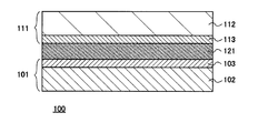
도 1은 축전 장치(100)의 단면도이다.1 is a sectional view of a
축전 장치(100)는, 부극(負極)(101)과, 정극(111)과, 부극(101) 및 정극(111)으로 협지(挾持)된 전해질(121)로 구성된다. 또한, 부극(101)은 부극 집전체(102) 및 부극 활물질층(103)으로 구성되어도 좋다. 정극(111)은 정극 집전체(112) 및 정극 활물질층(113)으로 구성되어도 좋다. 또한, 전해질(121)은 세퍼레이터에 유지되어 있다. 또한, 세퍼레이터는 부극 활물질층(103) 및 정극 활물질층(113)과 접한다.The
부극 집전체(102) 및 정극 집전체(112)는 각각 다른 외부 단자와 접속한다. 또한, 부극(101)과 전해질(121)을 포함한 세퍼레이터 및 정극(111)은 도시되지 않은 외장 부재로 덮여 있다.The negative electrode
또한, 활물질이란 캐리어인 이온의 삽입 및 탈리에 관한 물질을 가리킨다. 도포법에 의하여 정극 및 부극 등의 전극을 제작하는 경우에는, 표면에 탄소층이 형성된 활물질과 함께 도전조제나 바인더, 용매 등의 다른 재료를 혼합한 것을 활물질층으로서 집전체 위에 형성하는 경우가 있다. 이 경우, 활물질과 활물질층은 구별된다.The active material refers to a substance relating to insertion and desorption of ions which are carriers. When an electrode such as a positive electrode and a negative electrode is formed by a coating method, a mixture of an active material having a carbon layer on its surface and other materials such as a conductive additive, a binder, and a solvent may be formed on the current collector as an active material layer . In this case, the active material and the active material layer are distinguished.
정극 집전체(112) 위에 정극 활물질층(113)을 형성함으로써, 정극(111)을 형성한다. 또한, 부극 집전체(102) 위에 부극 활물질층(103)을 형성함으로써, 부극(101)을 형성한다. 나중에 서술하지만, 부극 활물질층(103)이 부극 집전체(102)로서 충분한 도전성을 갖는 경우에는, 부극 활물질층(103) 단체(單體)를 부극(101)으로 하여도 좋다. 정극 활물질층(113) 및 부극 활물질층(103) 사이에 전해질(121)을 협지시킴으로써, 축전 장치(100)를 제작한다.The positive electrode
또한, 상술한 바와 같이, 전해질(121)은 세퍼레이터에 유지되어도 좋고, 나중에 서술하는 바와 같이, 세퍼레이터가 필요 없는 경우에는, 전해질(121) 자체를 정극(111) 및 부극(101) 사이, 더 구체적으로는 정극 활물질층(113) 및 부극 활물질층(103) 사이에 배치한다.As described later, when the separator is not required, the
본 실시형태에 나타낸 축전 장치(100)에 포함된 정극(111)에 대하여 설명한다.The
정극 집전체(112)는 티타늄, 스테인리스, 백금, 알루미늄, 구리 등의 도전성이 높은 재료를 사용할 수 있다. 또한, 상기 도전성이 높은 재료를 적층하여도 좋다. 또한, 정극 집전체(112)는, 박(箔) 형상, 판 형상, 막 형상 등의 형상을 적절히 사용할 수 있다. 본 실시형태에서는, 정극 집전체(112)로서 막 두께 100μm의 티타늄막 또는 스테인리스막을 사용한다.As the positive electrode
정극 활물질층(113)으로서, 코발트산 리튬(LiCoO2)층을 사용한다. 상기 코발트산 리튬(LiCoO2)층은 정극 집전체(112)를 400℃ 이상 600℃ 미만의 온도로 가열하면서, 스퍼터링법에 의하여 형성된다. 상기 스퍼터링법으로는, 코발트산 리튬을 타깃으로 하고, 정극 집전체(112)로서 사용하는 티타늄막 또는 스테인리스막 위에 코발트산 리튬층을 막 두께 100nm 이상 100μm 이하로 형성한다.As the positive electrode
본 실시형태에 있어서, 스퍼터링 장치로서 "스퍼터링 장치 EB1000"(Canon ANELVA Corporation 제작)을 사용하여, 주파수 13.56MHz, 전력 30W, 압력 0.5Pa, 아르곤(Ar) 유량 10sccm, 기판(정극 집전체(112)) 및 타깃간 거리 75mm, 기판 회전 속도 5rpm로 형성하였다. 또한, 정극 집전체(112)의 온도로서 정극 집전체(112)를 가열하는 히터의 온도를 측정하였다.(Positive electrode current collector 112) at a frequency of 13.56 MHz, a power of 30 W, a pressure of 0.5 Pa, an argon (Ar) flow rate of 10 sccm, ) And a target distance of 75 mm, and a substrate rotation speed of 5 rpm. The temperature of the heater for heating the
정극 집전체(112)를 400℃ 이상 600℃ 미만의 온도로 가열하면서, 스퍼터링법에 의하여 코발트산 리튬층을 형성하면, 상기 코발트산 리튬층은 c축 배향된 결정성 코발트산 리튬층이 된다.When the lithium cobalt oxide layer is formed by the sputtering method while heating the
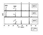
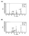
정극 집전체(112)로서 두께 100μm의 티타늄박을 사용하고, 정극 집전체(112)를 300℃, 400℃, 500℃로 가열하며, 정극 활물질층(113)인 코발트산 리튬층을 100nm의 두께로 형성한 경우의 X선 회절계(X-ray diffractometer: XRD)에 의한 측정 결과를 도 2에서 도시하였다. 도 2에 있어서, 동그라미(○)는 코발트산 리튬 유래의 피크, 삼각형(△)은 티타늄 유래의 피크를 나타낸 것이다.The positive electrode
도 2에 있어서, 정극 집전체(112)를 400℃ 및 500℃로 가열하면서 형성한 코발트산 리튬층에는, (003)면의 피크 및 (006)면의 피크가 보인다. (003)면의 피크 및 (006)면의 피크가 보인다는 것은, 코발트산 리튬층이 정극 집전체(112) 표면에 대하여 수직 방향으로 c축 배향된 상태인 것을 나타낸다.In Fig. 2, the peak of the (003) plane and the peak of the (006) plane are seen in the lithium cobalt oxide layer formed while heating the positive electrode
한편, 정극 집전체(112)를 300℃로 가열하면서 형성한 코발트산 리튬층에는, (003)면의 피크도 보이지 않는다. 즉, 정극 집전체(112)를 300℃로 가열하면서 형성한 코발트산 리튬층에서는, 정극 집전체(112) 표면에 대하여 c축 배향되지 않은 상태인 것을 나타낸다.On the other hand, no peak of the (003) plane is seen in the lithium cobalt oxide layer formed while heating the positive electrode
도 3에서 정극 집전체(112)로서 스테인리스(SUS316L)를 사용한 경우의 XRD에 의한 측정 결과를 도시하였다.Fig. 3 shows the results of XRD measurement when stainless steel (SUS316L) is used as the
도 3에서는, 정극 집전체(112)로서 막 두께 100μm의 스테인리스막을 사용하고, 정극 집전체(112)를 500℃로 가열하면서, 정극 활물질층(113)으로서 코발트산 리튬층을 막 두께 300nm로 형성하였다.3, a stainless steel film having a thickness of 100 탆 is used as the
도 3에서 코발트산 리튬층을 XRD로 측정한 결과를 도시하였다. 도 3에 있어서, 동그라미(○)는 코발트산 리튬 유래의 피크, 사각형(□)은 스테인리스에 함유된 철(Fe) 또는 크롬(Cr) 유래의 피크를 나타낸 것이다.FIG. 3 shows the results of XRD measurement of the lithium cobalt oxide layer. In Fig. 3, circles indicate peaks derived from lithium cobalt oxide, and squares indicate peaks derived from iron (Fe) or chromium (Cr) contained in stainless steel.
도 3에서 도시한 바와 같이, 정극 집전체(112)가 스테인리스막이라도, 코발트산 리튬층에는 (003)면의 피크 및 (006)면의 피크가 관측되었다. 상술한 바와 같이, (003)면의 피크 및 (006)면의 피크가 관측되는 것은 코발트산 리튬층이 정극 집전체(112) 표면에 대하여 수직 방향으로 c축 배향한다는 것을 나타낸다.3, the peak of the (003) plane and the peak of the (006) plane were observed in the lithium cobalt oxide layer even when the positive electrode
상술한 XRD 측정에 의하여, 정극 집전체(112)를 400℃ 및 500℃로 가열하면서 형성한 코발트산 리튬층은, 정극 집전체(112) 표면에 대하여 수직 방향으로 c축 배향한 결정성 코발트산 리튬층인 것이 제시되었다. 또한, 도 2를 보면 알 수 있듯이 코발트산 리튬의 분해 생성물의 피크는 검출되지 않았다. 따라서, 정극 집전체(112)를 400℃ 및 500℃로 가열하면서 형성한 코발트산 리튬층은, 가열에 의하여 분해되지 않고, 분해 생성물이 생성되지 않은 것이 제시되었다. 또한, 도 2를 보면 알 수 있듯이, 티타늄 유래의 피크가 검출되었지만, 산화 티타늄 유래의 피크는 검출되지 않았다. 따라서, 정극 집전체(112)로서 사용한 티타늄막과 코발트산 리튬층은 반응하지 않았다.By the above-described XRD measurement, the lithium cobalt oxide layer formed while heating the positive electrode
도 6(A) 및 도 6(B)에서, 성막시에 가열하지 않으며 형성하고, 형성한 후에 고온(600℃)으로 가열하였을 때의 코발트산 리튬의 XRD 측정의 결과를 도시하였다.6 (A) and 6 (B) show the results of XRD measurement of lithium cobalt oxide when heated at a high temperature (600 ° C) after forming, forming, and not heating at the time of film formation.
정극 집전체(112)로서 막 두께 100μm의 티타늄막을 사용하고, 정극 집전체(112)를 가열하지 않고 정극 활물질층(113)으로서 코발트산 리튬층을 막 두께 100nm로 형성하였다. 코발트산 리튬층을 형성한 후, 질소 및 아르곤 분위기 중에서 600℃로 20시간 가열한 경우의 XRD 측정 결과를 도 6(A)에서 도시하고, 진공 분위기 중에서 600℃로 60시간 가열한 경우의 XRD 측정 결과를 도 6(B)에서 도시하였다. 도 6(A) 및 도 6(B)에 있어서, 동그라미(○)는 코발트산 리튬 유래의 피크, 삼각형(△)은 티타늄 유래의 피크, 가위표(×)는 산화 티타늄(TiO2) 유래의 피크를 나타낸다.A lithium cobalt oxide layer having a thickness of 100 nm was formed as the positive electrode
도 6(A)에서는, 코발트산 리튬의 (012)면의 피크 및 (113)면의 피크가 검출되었다. (012)면의 피크 및 (113)면의 피크가 검출된 것은 상기 코발트산 리튬이 c축 배향되지 않은 것을 나타낸다.In FIG. 6 (A), a peak of the (012) plane and a peak of the (113) plane of lithium cobalt oxide were detected. The peak of the (012) plane and the peak of the (113) plane were detected, indicating that the lithium cobalt oxide was not c-axis oriented.
또한, 도 6(B)에서는 코발트산 리튬의 (012)면의 피크 및 (104)면의 피크가 검출되었다. 코발트산 리튬의 (012)면의 피크 및 (104)면의 피크가 검출된 것은 상기 코발트산 리튬이 c축 배향되지 않은 것을 나타낸다.6 (B), a peak of the (012) plane and a peak of the (104) plane of lithium cobalt oxide were detected. The peak of the (012) plane and the peak of the (104) plane of lithium cobalt oxide were detected, indicating that the lithium cobalt oxide was not c-axis oriented.
도 6(A) 및 도 6(B)의 강도(Intensity) 0부근을 확대한 도면을 각각 도 8(A) 및 도 8(B)에서 도시하였다. 또한, 도 8(A) 및 도 8(B)에 있어서 다이아몬드형(◇)은 산화 코발트(Co3O4) 유래의 피크를 나타낸다.Figs. 8A and 8B show enlarged views of the vicinity of the
도 8(A) 및 도 8(B)에서 도시한 바와 같이, 600℃로 코발트산 리튬을 가열하면, 코발트산 리튬이 분해되어, 분해 생성물인 산화 코발트가 생성된다. 이와 같이, 분해 생성물이 생성되고, 코발트산 리튬보다 많아지면, 충전 및 방전 용량이 작아질 우려가 있다. 실제로 충전 및 방전 용량의 측정을 행한 결과에 대해서는, 나중에 서술하기로 한다.As shown in Figs. 8 (A) and 8 (B), when lithium cobalt oxide is heated to 600 deg. C, lithium cobalt oxide is decomposed to produce cobalt oxide which is a decomposition product. As described above, decomposition products are produced, and if the amount is larger than lithium cobalt oxide, the charging and discharging capacity may be reduced. The results of actually measuring the charging and discharging capacities will be described later.
또한, 도 6(A) 및 도 6(B)의 양쪽에 있어서 산화 티타늄(TiO2) 유래의 피크가 검출되었다. 상술한 바와 같이, 산화 티타늄은 코발트산 리튬 중의 산소가 집전체의 티타늄과 반응하여 형성된 것이다. 이와 같이, 집전체의 티타늄이 산화 티타늄이 되면 집전체의 저항이 높아진다. 또한, 코발트산 리튬으로부터 산소가 추출됨으로써, 코발트산 리튬에 결정 결함이 생기거나, 또는 코발트산 리튬의 결정 구조가 변화하게 된다.Further, peaks derived from titanium oxide (TiO 2 ) were detected in both of Fig. 6 (A) and Fig. 6 (B). As described above, titanium oxide is formed by reacting oxygen in the lithium cobalt oxide with titanium in the current collector. Thus, when the titanium of the current collector becomes titanium oxide, the resistance of the current collector becomes high. Further, when oxygen is extracted from lithium cobalt oxide, crystal defects occur in lithium cobalt oxide or the crystal structure of lithium cobalt oxide changes.
따라서, 도 6(A) 및 도 6(B)에 의하여, 고온(600℃)으로 가열된 코발트산 리튬은 분해되어 분해 생성물이 생성되는 것, c축으로 배향하지 않는 것, 및 집전체인 티타늄과 반응하는 것이 제시되었다.6 (A) and 6 (B) show that the lithium cobalt oxide heated to a high temperature (600 ° C) decomposes to produce decomposition products, that it is not oriented in the c-axis, .
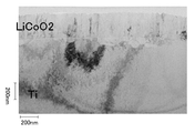
도 10에 정극 집전체(112)로서, 막 두께 100μm의 티타늄(Ti)막을 사용하고, 정극 집전체(112)를 500℃로 가열하면서 정극 활물질층(113)으로서 코발트산 리튬(LiCoO2)층을 스퍼터링법으로 두께 300nm로 형성한 정극(111)을 전자선 회절로 관찰한 결과를 도시하였다.10, a titanium (Ti) film having a thickness of 100 탆 is used as the
도 10에서 도시한 바와 같이, 전자선 회절 스폿의 귀속 및 입사 방위를 동정하였다. (000) 스폿을 기점(基点)으로 평행 사변형을 형성하는 3개의 회절 스폿의 위치 관계에 있어서, [0001] 방향에서 관찰하였을 때 얻은 회절 스폿의 위치 관계와 일치하였다. 이로써, 본 실시형태의 코발트산 리튬층이 c축으로 배향하고 있는 것이 증명되었다.As shown in Fig. 10, the attribution of the electron beam diffraction spot and the incident orientation were identified. And the positional relationship of the three diffraction spots forming the parallelogram with the (000) spot as a base point coincided with the positional relationship of the diffraction spots obtained when observed in the [0001] direction. As a result, it was proved that the lithium cobalt oxide layer of this embodiment is oriented in the c-axis direction.
도 4에서, 도 10과 마찬가지로 형성한 정극(111)의 투과형 전자 현미경(TEM: Transmission Electron Microscope)으로 관찰한 결과를 도시하였다.In FIG. 4, the result of observation with a transmission electron microscope (TEM) of the
도 4에는, 티타늄(Ti)막 표면에 대하여 수직 방향으로 연장된 코발트산 리튬(LiCoO2)의 기둥 형상 결정립이 관찰되었다.In Fig. 4, columnar crystal grains of lithium cobalt oxide (LiCoO 2 ) extending in the direction perpendicular to the surface of the titanium (Ti) film were observed.
이상, 본 실시형태에 의하여, 코발트산 리튬이 분해되어, 분해 생성물이 생성되는 것을 억제할 수 있다.As described above, according to the present embodiment, generation of decomposition products can be suppressed by decomposing lithium cobalt oxide.
또한, 본 실시형태에 의하여, 코발트산 리튬 중의 산소가 집전체와 반응하는 것을 억제할 수 있다.Further, according to the present embodiment, it is possible to inhibit the oxygen in the lithium cobalt oxide from reacting with the current collector.
다음에, 본 실시형태에 나타낸 축전 장치(100)에 포함된 부극(101)에 대하여 설명한다.Next, the
부극 집전체(102)는, 구리, 스테인리스, 철, 니켈 등의 도전성이 높은 재료를 사용할 수 있다. 부극 집전체(102)는, 박 형상, 판 형상, 막 형상 등의 형상을 적절히 사용할 수 있다.As the
부극 활물질층(103)에는, 리튬 이온의 흡장(吸藏) 및 방출이 가능한 재료를 사용한다. 대표적으로는, 리튬, 알루미늄, 흑연, 실리콘, 주석, 게르마늄 등이 사용된다. 부극 활물질층(103)이 부극 집전체(102)로서 충분히 기능할 수 있는 도전성을 갖는 경우에는, 부극 활물질층(103)이 부극 집전체(102)를 겸하여도 좋다. 즉, 부극 활물질층(103)이 부극 집전체(102)로서 충분히 기능할 수 있는 도전성을 갖는 경우에는, 부극 활물질층(103)을 단체로 부극(101)으로서 사용하여도 좋다.In the negative electrode
또한, 흑연과 비교하면, 게르마늄, 실리콘, 리튬, 알루미늄의 이론 리튬 흡장(吸藏) 용량이 크다. 흡장 용량이 크면, 작은 면적이라도 충분하게 충전 및 방전을 행할 수 있고, 부극으로서 기능하기 때문에 비용의 절감 및 2차 전지의 소형화로 이어진다. 다만, 실리콘 등은 리튬을 흡장하여 체적이 4배 정도까지 증가하기 때문에, 재료 자체가 취약(脆弱)화하는 것에 충분히 조심해야 된다.Compared with graphite, the theoretical lithium absorption capacity of germanium, silicon, lithium and aluminum is large. If the storage capacity is large, charging and discharging can be performed sufficiently even with a small area, and it functions as a negative electrode, resulting in cost reduction and miniaturization of the secondary battery. However, since silicon absorbs lithium and the volume thereof increases to about four times, it is necessary to be careful enough that the material itself becomes weak (fragile).
또는, 부극 활물질층(103)으로서 리튬이 아닌 재료를 사용한 경우, 부극 활물질층(103)에 리튬을 프리 도핑(pre-doping)하여도 좋다. 리튬을 프리 도핑하는 방법으로서는, 스퍼터링법에 의하여 부극 활물질층(103) 표면 위에 리튬층을 형성하여도 좋다. 또는 부극 활물질층(103) 표면 위에 리튬 박(箔)을 배치함으로써 부극 활물질층(103)에 리튬을 프리 도핑할 수 있다. 또한, 본 명세서에서는, 부극 활물질층에 리튬을 프리 도핑한 것도 부극 활물질층이라고 부른다.Alternatively, when a non-lithium material is used as the negative electrode
부극 활물질층(103)의 두께는 100nm 이상 100μm 이하에서 원하는 두께를 선택한다.The thickness of the negative electrode
또한, 부극 활물질층(103)에는 바인더, 도전조제를 가져도 좋다. 또한, 부극 활물질층(103) 표면에 전해질(121)과의 접촉성을 개선하기 위한 층을 형성하여도 좋다.The negative electrode
또한, 상기 바인더로서는, 다당류, 열가소성 수지 또는 고무 탄성을 갖는 폴리머 등을 들 수 있다. 예를 들어, 전분, 카르복시메틸셀룰로오스, 히드록시프로필셀룰로오스, 재생 셀룰로오스, 디아세틸셀룰로오스, 폴리비닐클로라이드, 폴리비닐피롤리돈, 폴리테트라플루오로에틸렌, 폴리불화비닐리덴, 폴리에틸렌, 폴리프로필렌, EPDM(Ethylene Propylene Diene Monomer), 술폰화 EPDM, 스티렌부타디엔고무, 부타디엔고무, 불소고무 등을 사용할 수 있다. 그 이외에 폴리이미드나 폴리비닐 알코올, 폴리에틸렌 옥사이드 등을 사용하여도 좋다.Examples of the binder include a polysaccharide, a thermoplastic resin, a polymer having rubber elasticity, and the like. For example, there may be mentioned starch, carboxymethylcellulose, hydroxypropylcellulose, regenerated cellulose, diacetylcellulose, polyvinylchloride, polyvinylpyrrolidone, polytetrafluoroethylene, polyvinylidene fluoride, polyethylene, polypropylene, EPDM Ethylene Propylene Diene Monomer), sulfonated EPDM, styrene butadiene rubber, butadiene rubber, fluorine rubber and the like. Polyimide, polyvinyl alcohol, polyethylene oxide, or the like may be used.
도전조제는, 그 재료 자체가 전자 도전체이며, 축전 장치 내에서 다른 물질과 화학 변화를 일으키지 않는 것이라면 좋다. 예를 들어, 흑연(黑鉛), 탄소 섬유, 카본 블랙, 아세틸렌 블랙, VGCF(상표 등록) 등의 탄소계 재료, 구리, 니켈, 알루미늄 또는 은 등 금속 재료 또는 이들의 혼합물의 분말이나 섬유 등이 그것에 상당한다. 도전조제란 활물질들 사이의 도전성을 도와주는 물질이고, 떨어진 활물질들 사이에 충전되어 활물질들이 도통되게 하는 재료이다.The conductive additive may be any material whose material itself is an electronic conductor and does not cause chemical change with other materials in the electrical storage device. For example, carbon-based materials such as graphite, carbon fiber, carbon black, acetylene black and VGCF (registered trademark), or powders or fibers of metal materials such as copper, nickel, It corresponds to that. A conductive auxiliary agent is a material that helps conductivity between active materials, and is a material that is charged between separated active materials so that active materials are conducted.
본 실시형태의 부극 활물질층(103)은 상술한 리튬 이온의 흡장 및 방출이 가능한 재료를 부극 집전체(102) 위에 스퍼터링법 등으로 막으로서 형성하여도 좋다. 또한, 상술한 바와 같이, 상기 리튬 이온의 흡장 및 방출이 가능한 재료로 형성된 막에 리튬을 프리 도핑하여도 좋다.The negative electrode
또는, 상술한 리튬 이온의 흡장 및 방출이 가능한 재료, 바인더, 도전조제, 및 유기 용제를 혼합하여 슬러리를 형성한다. 상기 슬러리를 부극 집전체(102) 위에 형성하고, 건조, 및 소성을 행함으로써, 본 실시형태의 부극 활물질층(103)을 형성하여도 좋다. 이와 같이, 본 실시형태의 부극 활물질층(103)을 형성한 경우에도, 슬러리 형성, 건조, 및 소성을 행한 후, 리튬을 프리 도핑하여도 좋다.Alternatively, a slurry is formed by mixing a material capable of intercalating and deintercalating lithium ions, a binder, a conductive additive, and an organic solvent. The negative electrode
다음에, 본 실시형태에 나타낸 축전 장치(100)에 포함된 전해질(121)에 대하여 설명한다.Next, the
전해질(121)의 용질은, 캐리어 이온인 리튬 이온을 이송할 수 있고, 또 리튬 이온이 안정적으로 존재하는 재료를 적절히 사용한다.The solute of the
전해질(121)의 용질의 대표적인 예로서는, LiPF6, LiClO4, LiAsF6, LiBF4, Li(C2F5SO2)2N 등의 리튬염을 들 수 있다.Representative examples of the solute electrolyte in (121), LiPF 6, LiClO 4, LiAsF 6, LiBF 4, Li (C 2
또한, 전해질(121)의 용매로서는, 리튬 이온의 이송이 가능한 재료를 사용한다. 전해질(121)의 용매로서는, 비프로톤성 유기 용매(aprotic organic solvent)가 바람직하다. 비프로톤성 유기 용매의 대표적인 예로서는, 에틸렌카보네이트, 프로필렌카보네이트, 디메틸카보네이트, 디에틸카보네이트, γ-부티로락톤, 아세토니트릴, 디메톡시에탄, 테트라하이드로푸란 등이 있고, 이들의 하나 또는 복수를 사용할 수 있다.As the solvent of the
전해질(121)의 용매가 점성이 낮은 액체인 경우, 전해질(121)을 후술하는 세퍼레이터에 함침시켜, 상기 세퍼레이터를 정극(111) 및 부극(101) 사이, 보다 구체적으로는 부극 활물질층(103) 및 정극 활물질층(113)과 접하도록 배치한다.When the solvent of the
또한, 전해질(121)의 용매 대신에 겔(gel)을 사용함으로써, 누액성(liquid leakage)을 포함한 안정성이 높아진다. 또한, 리튬 이온 2차 전지의 박형화 및 경량화가 가능하다. 겔화의 대표적인 예로서는, 실리콘겔, 아크릴겔, 아크릴로니트릴겔, 폴리에틸렌옥사이드겔, 폴리프로필렌옥사이드겔, 불소계 폴리머겔 등이 있다.Further, by using a gel instead of the solvent of the
이와 같이, 전해질(121)의 용매 대신에 겔을 사용한 경우, 반드시 세퍼레이터를 제공할 필요는 없다. 세퍼레이터의 유무는 상기 겔에 따라 결정하면 좋다. 세퍼레이터를 제공하지 않은 경우에는, 전해질(121) 자체를 세퍼레이터 대신에 정극(111) 및 부극(101) 사이, 보다 구체적으로는 부극 활물질층(103) 및 정극 활물질층(113)과 접하도록 배치한다.As described above, when a gel is used instead of the solvent of the
또한, 전해질(121)로서, Li3PO4 등의 고체 전해질을 사용할 수 있다. 이와 같은 고체 전해질을 전해질(121)로서 사용한 경우에도, 전해질(121) 자체를 정극(111) 및 부극(101) 사이에 배치할 수 있다.As the
세퍼레이터는, 절연성의 다공체(多孔體)를 사용한다. 세퍼레이터의 대표적인 예로서는, 셀룰로오스(종이), 폴리에틸렌, 폴리프로필렌 등이 있다.As the separator, an insulating porous body is used. Representative examples of the separator include cellulose (paper), polyethylene, and polypropylene.
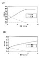
이하에, 상술한 축전 장치의 충전 및 방전 특성에 대하여 도 5(A) 내지 도 5(C)를 사용하여 설명한다.Hereinafter, the charging and discharging characteristics of the above-described power storage device will be described with reference to Figs. 5 (A) to 5 (C).
본 실시형태의 축전 장치에서는, 정극 집전체(112)로서 막 두께 100μm의 티타늄막을 사용하고, 정극 집전체(112)를 300℃, 400℃, 500℃로 가열하면서 정극 활물질층(113)으로서 코발트산 리튬층을 막 두께 100nm로 형성한 정극(111)을 사용하였다. 또한, 상기 코발트산 리튬층의 XRD 측정의 결과는 도 2에 도시되었다.In the electrical storage device of this embodiment, a titanium film having a thickness of 100 mu m is used as the positive electrode
본 실시형태의 축전 장치의 충전 및 방전 측정은, 충방전 시험 장치 TOSCAT-3100(TOYO SYSTEM Co., LTD제)을 사용하여 행하였다. 측정 전압은 2.5V 내지 4.2V의 범위로 설정하였다. 충전시에는, 소정의 전류값으로 충전을 행하고, 상기 전류값으로 소정의 전압(본 실시형태에서는 4.2V)까지 도달한 후에는, 상기 소정의 전압으로 충전을 유지한 정전류 정전압(CCCV) 측정을 행하였다. 또한, 방전시에는 소정의 전류값으로 충전을 행하는 정전류(CC) 측정을 행하였다.Charging and discharging measurement of the electrical storage device of the present embodiment was performed using a charge-discharge test apparatus TOSCAT-3100 (manufactured by TOYO SYSTEM Co., LTD.). The measurement voltage was set in the range of 2.5V to 4.2V. At the time of charging, charging is performed at a predetermined current value. After reaching a predetermined voltage (4.2 V in this embodiment) as the current value, a constant current constant voltage (CCCV) measurement in which charging is maintained at the predetermined voltage is performed . Further, at the time of discharging, a constant current (CC) measurement in which charging was performed at a predetermined current value was performed.
정전류의 전류값은 1μA, 정전압으로 고정한 후에는 전류값이 0.1μA가 되었을 때 측정을 종료하였다. 또한, 충전 및 방전의 중지 시간은 2시간으로 하였다. 또한, 본 전류의 충전 및 방전 측정은 정전류의 충전 및 방전을 3번 행한 후에 행해졌다.The measurement was terminated when the current value of the constant current was 1 μA and the current value was 0.1 μA after the voltage was fixed at the constant voltage. The charging and discharging stop time was set to 2 hours. The charging and discharging measurement of this current was performed after charging and discharging of the constant current three times.
또한, 본 실시형태의 축전 장치에서는, 부극 활물질층(103)으로서 금속 리튬(Li)막을 사용하였다. 금속 리튬(Li)막은 집전체로서도 기능하기 때문에, 부극(101)으로서는 상기 금속 리튬(Li)막만을 사용하였다. 또한, 전해질(121)의 용질로서 LiPF6, 전해질(121)의 용매로서 에틸렌카보네이트 및 디에틸카보네이트를 사용한다. 또한, 전해질(121)을 함유한 세퍼레이터로서 폴리프로필렌을 사용하였다.In the electrical storage device of the present embodiment, a metal lithium (Li) film is used as the negative electrode
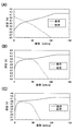
도 5(A), 도 5(B), 도 5(C) 각각에서, 상술한 가열 온도가 300℃, 400℃, 500℃일 때의 용량, 및 충전 및 방전 전압의 관계를 도시하였다. 또한, 각각의 가열 온도에 있어서의 최대 방전 용량은, 98.7mAh/g, 94mAh/g, 70.2mAh/g이었다.5A, 5B and 5C show the relationship between the capacity and the charging and discharging voltage when the above-described heating temperatures are 300 DEG C, 400 DEG C, and 500 DEG C, respectively. The maximum discharge capacities at the respective heating temperatures were 98.7 mAh / g, 94 mAh / g and 70.2 mAh / g.
또한, 방전 곡선에 있어서, 도 5(B)에서는, 방전 전압 3.6V 내지 3.7V에, 도 5(C)에서는 방전 전압 3.5V 내지 3.6V에 파형의 변위점이 관찰되었다. 한편, 도 5(A)에서는 변위점은 관찰되지 않았다. 이것은, 도 5(A)(300℃)와, 도 5(B)(400℃), 도 5(C)(500℃)에서는 서로 다른 충전 및 방전 반응이 일어나고 있기 때문이다.5B, waveforms of displacement waveforms were observed at discharge voltages of 3.6V to 3.7V and discharge voltages of 3.5V to 3.6V in Fig. 5C. On the other hand, no displacement point was observed in Fig. 5 (A). This is because different charging and discharging reactions occur in FIG. 5A (300 ° C.), FIG. 5B (400 ° C.) and FIG. 5C (500 ° C.).
도 7(A) 및 도 7(B)에서 각각, 도 6(A) 및 도 6(B)에서 사용한 코발트산 리튬층을 정극 활물질층(113)으로서 사용한 축전 장치의 용량, 및 충전 및 방전 전압의 관계를 도시하였다. 또한, 도 7(A) 및 도 7(B)에서 사용한 축전 장치의 최대 방전 용량은 각각 9.6mAh/g 및 12mAh/g이었다.Capacity of the power storage device using the lithium cobalt oxide layer used as the positive electrode
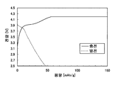
도 11에서, 정극 집전체(112)인 막 두께 100μm의 티타늄막을 600℃로 가열하면서 정극 활물질층(113)인 코발트산 리튬층을 막 두께 100nm로 형성한 정극(111)을 사용한 축전 장치의 용량 및, 충전 및 방전 전압의 관계를 도시하였다. 도 11에서 최대 방전 용량은 47mAh/g이었다.11, the capacity of a power storage device using a
도 11에서 도시한 바와 같이, 600℃로 가열하면서 형성한 코발트산 리튬층을 정극 집전체(112)로서 사용한 축전 장치는, 충전 및 방전 용량, 특히 방전 용량이 작은 것이 제시되었다. 그 충전 및 방전 용량은 저온(400℃ 이상 600℃ 미만, 보다 구체적으로는 400℃(도 5(B)) 및 500℃(도 5(C)))보다 작다. 또한, 도 7(A) 및 도 7(B)에서 도시한 바와 같이, 형성한 후에 고온(600℃)으로 가열된 코발트산 리튬층을 정극 활물질층(113)으로서 사용한 축전 장치는, 충전 및 방전 용량이 저온(400℃ 이상 600℃ 미만, 보다 구체적으로는 400℃(도 5(B)) 및 500℃(도 5(C)))보다 작다. 이와 같이, 고온(600℃)으로 형성된 코발트산 리튬층, 또는 고온(600℃)으로 가열된 코발트산 리튬층을 정극 활물질층(113)으로서 사용한 축전 장치의 충전 및 방전 용량이, 저온(400℃ 이상 600℃ 미만, 보다 구체적으로는 400℃ 및 500℃)으로 가열된 코발트산 리튬층을 정극 활물질층(113)으로서 사용한 축전 장치의 충전 및 방전 용량보다 작은 이유는, 코발트산 리튬층이 분해되어 분해 생성물, 예를 들어 산화 코발트가 생성되었기 때문이다.As shown in Fig. 11, a power storage device using a lithium cobalt oxide layer formed while being heated at 600 占 폚 as the
따라서, 본 실시형태에서 서술한 바와 같이, 저온(400℃ 이상 600℃ 미만, 보다 구체적으로는 400℃ 및 500℃)으로 가열 형성된 코발트산 리튬층을 정극 활물질층(113)으로서 사용함으로써, 충전 및 방전 용량이 큰 축전 장치를 얻을 수 있다.Therefore, as described in the present embodiment, by using the lithium cobalt oxide layer formed by heating at a low temperature (less than 400 캜 and less than 600 캜, more specifically, 400 캜 and 500 캜) as the positive electrode
이상, 본 실시형태에 의하여, 코발트산 리튬이 분해되어, 분해 생성물이 생성되는 것을 억제할 수 있다.As described above, according to the present embodiment, generation of decomposition products can be suppressed by decomposing lithium cobalt oxide.
이상, 본 실시형태에 의하여, 코발트산 리튬 중의 산소가 집전체와 반응하는 것을 억제할 수 있다.As described above, according to the present embodiment, it is possible to suppress the oxygen in the lithium cobalt oxide from reacting with the current collector.
또한, 본 실시형태에 의하여, 충전 및 방전 용량이 큰 축전 장치를 얻을 수 있다.
Further, according to the present embodiment, a power storage device having a large charging and discharging capacity can be obtained.
(실시형태 2)(Embodiment 2)
본 실시형태에서는, 실시형태 1과는 다른 구조를 갖는 축전 장치에 대하여 설명한다.In this embodiment, a power storage device having a structure different from that of the first embodiment will be described.
도 9(A)에서 도시한 축전 장치는, 기판(201), 기판(201) 위에 정극 집전체(202) 및 부극 집전체(204)를 갖는다. 기판(201) 및 정극 집전체(202) 위에는, 정극 활물질층(203)이 형성되어 있다. 또한, 정극 집전체(202)와 접하고 정극 활물질층(203)을 덮어, 고체 전해질층(206)이 형성되어 있다. 또한, 고체 전해질층(206)과 부극 집전체(204)에 접하여 부극 활물질층(205)이 형성되어 있다. 고체 전해질층(206) 및 부극 활물질층(205)을 덮어 정극 집전체(202) 및 부극 집전체(204)에 접하여 보호막(207)이 형성되어 있다.The power storage device shown in Fig. 9A has a positive electrode
도 9(B)에서 도시한 축전 장치는, 기판(211), 기판(211) 위에 고체 전해질층(216), 고체 전해질층(216)과 접하여 정극 활물질층(213) 및 부극 활물질층(215)이 형성되어 있다. 정극 활물질층(213) 위에 형성되고, 고체 전해질층(216)과 접하여 정극 집전체(212), 부극 활물질층(215) 위에 형성되고, 고체 전해질층(216)과 접하여 부극 집전체(214)가 형성되어 있다. 고체 전해질층(216)을 덮어, 보호막(217)이 형성되어 있다.9B includes a positive electrode
도 9(C)에서 도시한 축전 장치는, 정극 집전체(221) 위에 정극 활물질층(222)이 형성되어 있다. 정극 활물질층(222)을 덮어 고체 전해질층(225)이 형성되어 있다. 고체 전해질층(225) 위에 부극 활물질층(224) 및 부극 집전체(223)가 형성되어 있다. 정극 집전체(221) 위에 고체 전해질층(225) 및 부극 활물질층(224)을 덮어 부극 집전체(223)에 접하여 보호막(226)이 형성되어 있다.9 (C), the positive electrode
도 9(A)의 기판(201) 및 도 9(B)의 기판(211)은 예를 들어 유리 기판, 석영 기판, 마이카(mica) 기판을 사용한다.For example, a glass substrate, a quartz substrate, or a mica substrate is used as the
도 9(A)의 정극 집전체(202), 도 9(B)의 정극 집전체(212), 도 9(C)의 정극 집전체(221)는 실시형태 1의 정극 집전체(112)와 마찬가지다.The
또한, 도 9(A)의 정극 활물질층(203), 도 9(B)의 정극 활물질층(213), 도 9(C)의 정극 활물질층(222)은 실시형태 1의 정극 활물질층(113)과 마찬가지다.The positive electrode
또한, 도 9(A)의 부극 집전체(204), 도 9(B)의 부극 집전체(214), 도 9(C)의 부극 집전체(223)는 실시형태 1의 부극 집전체(102)와 마찬가지다.The
도 9(A)의 부극 활물질층(205), 도 9(B)의 부극 활물질층(215), 도 9(C)의 부극 활물질층(224)의 재료로서, TiO2, Li4Ti5O12, Nb2O5, NbTiOx, WO2, MoO2, 실리콘 및 실리콘 합금, 게르마늄 및 게르마늄 합금, 주석 및 주석 합금, 금속 리튬을 사용할 수 있다(상기 x는 양의 실수). 이들 재료를 사용하여 PVD(스퍼터링, 증착)법, PLD(펄스 레이저)법, AD(에어로졸 디포지션)법에 의하여 막 형상의 상기 부극 활물질층을 형성한다.As the material of the negative electrode
도 9(A)의 부극 활물질층(205), 도 9(B)의 부극 활물질층(215), 도 9(C)의 부극 활물질층(224)의 막 두께는, 100nm 이상 100μm 이하의 범위에서 원하는 두께를 선택한다.The film thicknesses of the negative electrode
또한, 도 9(A)의 부극 활물질층(205), 도 9(B)의 부극 활물질층(215), 도 9(C)의 부극 활물질층(224)의 재료로서, 금속 리튬 이외의 재료를 사용하는 경우, 리튬을 프리 도핑하여도 좋다. 예를 들어, 증착법을 사용하여 상술한 부극 활물질층을 형성하는 경우, 증착원으로서 상술한 재료 및 리튬을 사용하여 상술한 부극 활물질층에 리튬을 프리 도핑하면 좋다. 또한, 본 명세서에서는, 부극 활물질층에 리튬을 프리 도핑한 것도 부극 활물질층이라고 부른다.It is also possible to use a material other than metal lithium as the material of the negative electrode
또한, 상기 부극 활물질층 표면에 고체 전해질층과의 접촉성을 개선시키기 위한 층을 형성하여도 좋다.A layer for improving contact with the solid electrolyte layer may be formed on the surface of the negative electrode active material layer.
도 9(A)의 고체 전해질층(206), 도 9(B)의 고체 전해질층(216), 도 9(C)의 고체 전해질층(225)의 재료로서, Li3PO4, Li3PO4 - xNx, Li1 .3Al0 .3Ti1 .7P3O12, Li0.35La0.55TiO3, Li14ZnGe4O16, Li6BaLa2Ta2O12, Li7La3Zr2O12 등의 산화물 재료, LixPSy, Li2S-SiS2-Li3PO4, Li2S-SiS2-Li4SiO4, Li3 .25Ge0 .25P0 .75S4 등의 황화물 재료를 사용할 수 있다(상기 x, y는 양의 실수).As the material of the
이들 재료를 사용하고, 증착법, PVD(스퍼터링, 증착)법, PLD(펄스 레이저)법, AD(에어로졸 디포지션)법에 의하여 상기 고체 전해질층을 형성한다. 또한, 상기 고체 전해질층의 형상은 막 형상, 펠릿 형상, 판 형상이라면 좋다.These solid materials are used to form the solid electrolyte layer by a vapor deposition method, a PVD (sputtering and vapor deposition) method, a PLD (pulsed laser) method and an AD (aerosol deposition) method. The shape of the solid electrolyte layer may be a film, a pellet, or a plate.
도 9(A)의 보호막(207), 도 9(B)의 보호막(217), 도 9(C)의 보호막(226)으로서 질화 실리콘막, 질화산화 실리콘막, 산화 실리콘막, 산화질화 실리콘막, 불소계 수지, DLC(Diamond Like Carbon)를 사용할 수 있다.A silicon nitride film, a silicon nitride film, a silicon oxide film, a silicon oxynitride film (silicon oxynitride film) as the
본 실시형태는, 상기 실시형태와 적절히 조합하여 실시할 수 있다.
The present embodiment can be implemented in appropriate combination with the above embodiment.
101 : 부극 102 : 부극 집전체
103 : 부극 활물질층 111 : 정극
112 : 정극 집전체 113 : 정극 활물질층
121 : 전해질 201 : 기판
202 : 정극 집전체 203 : 정극 활물질층
204 : 부극 집전체 205 : 부극 활물질층
206 : 고체 전해질층 207 : 보호막
211 : 기판 212 : 정극 집전체
213 : 정극 활물질층 214 : 부극 집전체
215 : 부극 활물질층 216 : 고체 전해질층
217 : 보호막 221 : 정극 집전체
222 : 정극 활물질층 223 : 부극 집전체
224 : 부극 활물질층 225 : 고체 전해질층
226 : 보호막101: negative electrode 102: negative electrode collector
103: negative electrode active material layer 111: positive electrode
112: positive electrode current collector 113: positive electrode active material layer
121: electrolyte 201: substrate
202: positive electrode current collector 203: positive electrode active material layer
204: negative electrode collector 205: negative electrode active material layer
206: solid electrolyte layer 207: protective film
211: substrate 212: positive electrode collector
213: positive electrode active material layer 214: negative electrode collector
215: negative electrode active material layer 216: solid electrolyte layer
217: protective film 221: positive electrode collector
222: positive electrode active material layer 223: negative electrode collector
224: Negative electrode active material layer 225: Solid electrolyte layer
226: Shield
Claims (19)
A lithium cobalt oxide layer is formed on the positive electrode current collector by a sputtering method using a target containing lithium cobalt oxide and a sputtering gas containing Ar while heating the positive electrode collector at a temperature of 400 ° C or more and less than 600 ° C Wherein the method comprises the steps of:
상기 코발트산 리튬층에서 코발트산 리튬의 결정은 c축을 배향되고,
상기 정극 집전체를 가열할 때 산화 코발트는 생성되지 않는, 축전 장치의 제작 방법.
The method according to claim 1,
The crystal of lithium cobalt oxide in the lithium cobalt oxide layer is oriented in the c-axis,
Wherein cobalt oxide is not generated when the positive electrode current collector is heated.
상기 정극 집전체의 재료는, 티타늄, 스테인리스, 백금, 알루미늄으로 이루어진 그룹 중에서 선택된 하나인, 축전 장치의 제작 방법.
The method according to claim 1,
Wherein the material of the positive electrode current collector is one selected from the group consisting of titanium, stainless steel, platinum, and aluminum.
상기 정극 집전체의 재료는 티타늄인, 축전 장치의 제작 방법.
The method according to claim 1,
Wherein the material of the positive electrode current collector is titanium.
상기 정극 집전체의 재료는 스테인리스인, 축전 장치의 제작 방법.
The method according to claim 1,
Wherein the material of the positive electrode current collector is stainless steel.
상기 코발트산 리튬층을 형성하기 전에 기판 위에 상기 정극 집전체 및 부극 집전체를 형성하는 단계와;
상기 코발트산 리튬층을 덮고 상기 정극 집전체에 접하는 고체 전해질층을 형성하는 단계와;
상기 고체 전해질층과 상기 부극 집전체에 접하는 부극 활물질층을 형성하는 단계와;
상기 고체 전해질층과 상기 부극 활물질층을 덮고 상기 정극 집전체와 상기 부극 집전체에 접하는 보호막을 형성하는 단계를 더 포함하는, 축전 장치의 제작 방법.
The method according to claim 1,
Forming the positive electrode collector and the negative electrode collector on a substrate before forming the lithium cobalt oxide layer;
Forming a solid electrolyte layer covering the lithium cobalt oxide layer and contacting the positive electrode current collector;
Forming a negative electrode active material layer in contact with the solid electrolyte layer and the negative electrode collector;
Further comprising the step of forming a protective film covering the solid electrolyte layer and the negative electrode active material layer and in contact with the positive electrode collector and the negative electrode collector.
상기 부극 집전체의 재료는 구리, 스테인리스, 철, 니켈로 이루어진 그룹 중에서 선택된 하나인, 축전 장치의 제작 방법.
The method according to claim 6,
Wherein the material of the negative electrode current collector is one selected from the group consisting of copper, stainless steel, iron, and nickel.
상기 고체 전해질층의 재료는 Li3PO4, Li3PO4 - xNx, Li1 .3Al0 .3Ti1 .7P3O12, Li0.35La0.55TiO3, Li14ZnGe4O16, Li6BaLa2Ta2O12, Li7La3Zr2O12, LixPSy, Li2S-SiS2-Li3PO4, Li2S-SiS2-Li4SiO4, Li3 .25Ge0 .25P0 .75S4 중 하나이고,
x, y는 양의 실수인, 축전 장치의 제작 방법.
The method according to claim 6,
The material of the solid electrolyte layer is selected from the group consisting of Li 3 PO 4 , Li 3 PO 4 - x N x , Li 1 .3 Al 0 .3 Ti 1 .7 P 3 O 12 , Li 0.35 La 0.55 TiO 3 , Li 14 ZnGe 4 O 16 , Li 6 BaLa 2 Ta 2 O 12 , Li 7 La 3 Zr 2 O 12 , Li x PS y , Li 2 S-SiS 2 -Li 3 PO 4 , Li 2 S-SiS 2 -Li 4 SiO 4 , Li 3 .25 Ge 0 .25 P 0 .75 S 4 / RTI >
and x and y are positive real numbers.
상기 부극 활물질층의 재료는 TiO2, Li4Ti5O12, Nb2O5, NbTiOx, WO2, MoO2, 실리콘, 실리콘 합금, 게르마늄, 게르마늄 합금, 주석, 주석 합금, 금속 리튬 중 하나인, 축전 장치의 제작 방법.
The method according to claim 6,
The material of the negative electrode active material layer may be one of TiO 2 , Li 4 Ti 5 O 12 , Nb 2 O 5 , NbTiO x , WO 2 , MoO 2 , silicon, silicon alloy, germanium, germanium alloy, tin, tin alloy, Wherein said method comprises the steps of:
상기 보호막은 질화 실리콘막, 질화산화 실리콘막, 산화 실리콘막, 산화질화 실리콘막, 불소계 수지, DLC(Diamond Like Carbon) 중 하나인, 축전 장치의 제작 방법.
The method according to claim 6,
Wherein the protective film is one of a silicon nitride film, a silicon nitride oxide film, a silicon oxide film, a silicon oxynitride film, a fluororesin, and a diamond like carbon (DLC).
상기 코발트산 리튬층을 덮는 고체 전해질층을 형성하는 단계와;
상기 고체 전해질층에 접하는 부극 활물질층을 형성하는 단계와;
상기 부극 활물질층 위에 부극 집전체를 형성하는 단계와;
상기 정극 집전체, 상기 고체 전해질층, 상기 부극 활물질층, 및 상기 부극 집전체에 접하는 보호막을 형성하는 단계를 더 포함하는, 축전 장치의 제작 방법.
The method according to claim 1,
Forming a solid electrolyte layer covering the lithium cobalt oxide layer;
Forming a negative electrode active material layer in contact with the solid electrolyte layer;
Forming a negative electrode current collector on the negative electrode active material layer;
Further comprising the step of forming a protective film in contact with said positive electrode current collector, said solid electrolyte layer, said negative electrode active material layer, and said negative electrode current collector.
By heating the positive electrode current collector at a temperature of 400 DEG C or more and less than 600 DEG C while sputtering using a target containing lithium cobalt oxide and a sputtering gas containing Ar to form the positive electrode collector on either one of titanium and stainless steel And forming a lithium cobalt oxide layer.
A method of manufacturing a power storage device, comprising the step of forming the positive electrode according to claim 12.
상기 코발트산 리튬층을 덮고 상기 정극 집전체에 접하는 고체 전해질층을 형성하는 단계와;
상기 고체 전해질층과 상기 부극 집전체에 접하는 부극 활물질층을 형성하는 단계와;
상기 고체 전해질층과 상기 부극 활물질층을 덮는 상기 정극 집전체와 상기 부극 집전체에 접하는 보호막을 형성하는 단계를 포함하는, 축전 장치의 제작 방법.
Forming a positive electrode and a negative electrode current collector according to claim 12 on a substrate;
Forming a solid electrolyte layer covering the lithium cobalt oxide layer and contacting the positive electrode current collector;
Forming a negative electrode active material layer in contact with the solid electrolyte layer and the negative electrode collector;
And forming a protective film in contact with the positive electrode current collector and the negative electrode current collector covering the solid electrolyte layer and the negative electrode active material layer.
상기 부극 집전체의 재료는 구리, 스테인리스, 철, 니켈로 이루어진 그룹 중에서 선택된 하나인, 축전 장치의 제작 방법.
15. The method of claim 14,
Wherein the material of the negative electrode current collector is one selected from the group consisting of copper, stainless steel, iron, and nickel.
상기 고체 전해질층의 재료는 Li3PO4, Li3PO4 - xNx, Li1 .3Al0 .3Ti1 .7P3O12, Li0.35La0.55TiO3, Li14ZnGe4O16, Li6BaLa2Ta2O12, Li7La3Zr2O12, LixPSy, Li2S-SiS2-Li3PO4, Li2S-SiS2-Li4SiO4, Li3 .25Ge0 .25P0 .75S4 중 하나이고,
x, y는 양의 실수인, 축전 장치의 제작 방법.
15. The method of claim 14,
The material of the solid electrolyte layer is selected from the group consisting of Li 3 PO 4 , Li 3 PO 4 - x N x , Li 1 .3 Al 0 .3 Ti 1 .7 P 3 O 12 , Li 0.35 La 0.55 TiO 3 , Li 14 ZnGe 4 O 16 , Li 6 BaLa 2 Ta 2 O 12 , Li 7 La 3 Zr 2 O 12 , Li x PS y , Li 2 S-SiS 2 -Li 3 PO 4 , Li 2 S-SiS 2 -Li 4 SiO 4 , Li 3 .25 Ge 0 .25 P 0 .75 S 4 / RTI >
and x and y are positive real numbers.
상기 부극 활물질층의 재료는 TiO2, Li4Ti5O12, Nb2O5, NbTiOx, WO2, MoO2, 실리콘, 실리콘 합금, 게르마늄, 게르마늄 합금, 주석, 주석 합금, 금속 리튬 중 하나인, 축전 장치의 제작 방법.
15. The method of claim 14,
The material of the negative electrode active material layer may be one of TiO 2 , Li 4 Ti 5 O 12 , Nb 2 O 5 , NbTiO x , WO 2 , MoO 2 , silicon, silicon alloy, germanium, germanium alloy, tin, tin alloy, Wherein said method comprises the steps of:
상기 보호막은 질화 실리콘막, 질화산화 실리콘막, 산화 실리콘막, 산화질화 실리콘막, 불소계 수지, DLC(Diamond Like Carbon) 중 하나인, 축전 장치의 제작 방법.
15. The method of claim 14,
Wherein the protective film is one of a silicon nitride film, a silicon nitride oxide film, a silicon oxide film, a silicon oxynitride film, a fluororesin, and a diamond like carbon (DLC).
상기 코발트산 리튬층 위에 고체 전해질층을 형성하는 단계와;
상기 고체 전해질층에 접하는 부극 활물질층을 형성하는 단계와;
상기 부극 활물질층 위에 부극 집전체를 형성하는 단계와;
상기 정극 집전체, 상기 고체 전해질층, 상기 부극 활물질층, 및 상기 부극 집전체에 접하는 보호막을 형성하는 단계를 포함하는, 축전 장치의 제작 방법.
Forming the positive electrode according to claim 12;
Forming a solid electrolyte layer on the lithium cobalt oxide layer;
Forming a negative electrode active material layer in contact with the solid electrolyte layer;
Forming a negative electrode current collector on the negative electrode active material layer;
And forming a protective film in contact with the positive electrode current collector, the solid electrolyte layer, the negative electrode active material layer, and the negative electrode current collector.
Applications Claiming Priority (2)
| Application Number | Priority Date | Filing Date | Title |
|---|---|---|---|
| JP2011090685 | 2011-04-15 | ||
| JPJP-P-2011-090685 | 2011-04-15 |
Publications (1)
| Publication Number | Publication Date |
|---|---|
| KR20120117656A true KR20120117656A (en) | 2012-10-24 |
Family
ID=46993588
Family Applications (1)
| Application Number | Title | Priority Date | Filing Date |
|---|---|---|---|
| KR1020120037490A KR20120117656A (en) | 2011-04-15 | 2012-04-10 | Method for manufacturing positive electrode and power storage device |
Country Status (5)
| Country | Link |
|---|---|
| US (1) | US8404001B2 (en) |
| JP (2) | JP2012230889A (en) |
| KR (1) | KR20120117656A (en) |
| CN (2) | CN102738516B (en) |
| TW (1) | TWI580804B (en) |
Families Citing this family (15)
| Publication number | Priority date | Publication date | Assignee | Title |
|---|---|---|---|---|
| KR101264337B1 (en) * | 2010-08-13 | 2013-05-14 | 삼성에스디아이 주식회사 | Positive active material and lithium battery using it |
| JP5775598B2 (en) * | 2011-10-31 | 2015-09-09 | 株式会社日立製作所 | Lithium ion secondary battery |
| US10044061B2 (en) * | 2014-06-11 | 2018-08-07 | Los Alamos National Security, Llc | Methods for growth of lithium-rich antiperovskite electrolyte films and use thereof |
| DE102015007291A1 (en) | 2015-06-10 | 2016-12-15 | Forschungszentrum Jülich GmbH | Process for producing nanostructured layers |
| CN110114910A (en) | 2016-12-09 | 2019-08-09 | 株式会社半导体能源研究所 | Secondary cell and its manufacturing method |
| JP6400771B1 (en) * | 2017-04-11 | 2018-10-03 | 株式会社石井表記 | Decompression unit with heater and battery manufacturing device |
| FR3076062B1 (en) | 2017-12-21 | 2020-07-17 | Commissariat A L'energie Atomique Et Aux Energies Alternatives | REALIZATION OF A MICROELECTRONIC DEVICE COLLECTOR |
| CN113348568A (en) | 2019-01-25 | 2021-09-03 | 株式会社半导体能源研究所 | All-solid-state battery and method for manufacturing same |
| KR20210143747A (en) | 2019-03-26 | 2021-11-29 | 가부시키가이샤 한도오따이 에네루기 켄큐쇼 | Solid-state secondary battery and its manufacturing method |
| JPWO2020222067A1 (en) | 2019-04-30 | 2020-11-05 | ||
| CN113728481A (en) | 2019-04-30 | 2021-11-30 | 株式会社半导体能源研究所 | Apparatus for manufacturing solid-state secondary battery and method for manufacturing solid-state secondary battery |
| JPWO2020250078A1 (en) | 2019-06-12 | 2020-12-17 | ||
| CN114207872A (en) | 2019-08-09 | 2022-03-18 | 株式会社半导体能源研究所 | Negative electrode, secondary battery, and solid-state secondary battery |
| DE112020005049T5 (en) | 2019-10-18 | 2022-11-03 | Semiconductor Energy Laboratory Co., Ltd. | Secondary battery and manufacturing method therefor |
| FI20207064A1 (en) * | 2020-04-17 | 2021-10-18 | Pulsedeon Oy | Method for the manufacture of an energy storage device utilizing lithium and solid inorganic electrolytes |
Citations (5)
| Publication number | Priority date | Publication date | Assignee | Title |
|---|---|---|---|---|
| US20020187399A1 (en) * | 2001-06-11 | 2002-12-12 | Johnson Lonnie G. | Thin lithium film battery |
| JP2005235686A (en) * | 2004-02-23 | 2005-09-02 | Sony Corp | Positive electrode, battery and their manufacturing method |
| JP2008523567A (en) * | 2004-12-08 | 2008-07-03 | シモーフィックス,インコーポレーテッド | LiCoO2 deposition |
| KR100962032B1 (en) * | 2007-12-11 | 2010-06-08 | 지에스나노텍 주식회사 | Thin film battery having enhanced surface area of electrode and enhanced contact area between electrode and electrolyte and method for producing the same |
| JP2010522954A (en) * | 2007-03-26 | 2010-07-08 | シンベット・コーポレイション | Thin film lithium battery substrate |
Family Cites Families (9)
| Publication number | Priority date | Publication date | Assignee | Title |
|---|---|---|---|---|
| US4916035A (en) * | 1987-08-06 | 1990-04-10 | Matsushita Electric Industrial Co., Ltd. | Photoelectrochemical cells having functions as a solar cell and a secondary cell |
| JPH08130015A (en) * | 1994-10-27 | 1996-05-21 | Mitsubishi Cable Ind Ltd | Negative electrode material, its negative electrode, and lithium secondary battery |
| JPH11162451A (en) * | 1997-11-27 | 1999-06-18 | Matsushita Electric Ind Co Ltd | Lithium secondary battery, manufacture of paste for negative electrode of lithium secondary battery, and lithium secondary battery having paste for negative electrode prepared by its manufacture |
| US7094500B2 (en) * | 2001-04-24 | 2006-08-22 | Matsushita Electric Industrial Co., Ltd. | Secondary battery |
| US20040258984A1 (en) | 2003-04-14 | 2004-12-23 | Massachusetts Institute Of Technology | Integrated thin film batteries on silicon integrated circuits |
| CN101073171B (en) * | 2004-12-08 | 2010-09-22 | 希莫菲克斯公司 | Deposition of licoo2 |
| US7862927B2 (en) * | 2007-03-02 | 2011-01-04 | Front Edge Technology | Thin film battery and manufacturing method |
| JP5195049B2 (en) | 2008-06-06 | 2013-05-08 | トヨタ自動車株式会社 | Lithium ion secondary battery and manufacturing method thereof |
| CN101814633A (en) * | 2009-02-19 | 2010-08-25 | 邓梁 | Filling solidification method for producing positive electrode and negative electrode of lithium battery and lithium battery containing positive electrode and negative electrode |
-
2012
- 2012-03-30 US US13/435,127 patent/US8404001B2/en active Active
- 2012-04-10 KR KR1020120037490A patent/KR20120117656A/en active Search and Examination
- 2012-04-10 JP JP2012089322A patent/JP2012230889A/en not_active Withdrawn
- 2012-04-12 TW TW101113022A patent/TWI580804B/en not_active IP Right Cessation
- 2012-04-13 CN CN201210124226.3A patent/CN102738516B/en not_active Expired - Fee Related
- 2012-04-13 CN CN201610118122.XA patent/CN105679998B/en active Active
-
2016
- 2016-12-22 JP JP2016248676A patent/JP2017069220A/en not_active Withdrawn
Patent Citations (5)
| Publication number | Priority date | Publication date | Assignee | Title |
|---|---|---|---|---|
| US20020187399A1 (en) * | 2001-06-11 | 2002-12-12 | Johnson Lonnie G. | Thin lithium film battery |
| JP2005235686A (en) * | 2004-02-23 | 2005-09-02 | Sony Corp | Positive electrode, battery and their manufacturing method |
| JP2008523567A (en) * | 2004-12-08 | 2008-07-03 | シモーフィックス,インコーポレーテッド | LiCoO2 deposition |
| JP2010522954A (en) * | 2007-03-26 | 2010-07-08 | シンベット・コーポレイション | Thin film lithium battery substrate |
| KR100962032B1 (en) * | 2007-12-11 | 2010-06-08 | 지에스나노텍 주식회사 | Thin film battery having enhanced surface area of electrode and enhanced contact area between electrode and electrolyte and method for producing the same |
Non-Patent Citations (2)
| Title |
|---|
| 일본 공표특허공보 특표2008-523567호(2008.07.03.) 1부. * |
| 일본 공표특허공보 특표2010-522954호(2010.07.08.) 1부. * |
Also Published As
| Publication number | Publication date |
|---|---|
| CN105679998B (en) | 2019-09-10 |
| CN105679998A (en) | 2016-06-15 |
| TWI580804B (en) | 2017-05-01 |
| JP2012230889A (en) | 2012-11-22 |
| US20120260478A1 (en) | 2012-10-18 |
| JP2017069220A (en) | 2017-04-06 |
| US8404001B2 (en) | 2013-03-26 |
| TW201245477A (en) | 2012-11-16 |
| CN102738516B (en) | 2016-03-30 |
| CN102738516A (en) | 2012-10-17 |
Similar Documents
| Publication | Publication Date | Title |
|---|---|---|
| KR20120117656A (en) | Method for manufacturing positive electrode and power storage device | |
| JP6705384B2 (en) | Lithium secondary battery | |
| US9742036B2 (en) | Anode material, anode and battery | |
| US10074854B2 (en) | Anode active material and all solid secondary battery | |
| US9123960B2 (en) | Solid-state electrolyte battery and cathode activating substance | |
| US9614224B2 (en) | Cathode active material for lithium battery, lithium battery, and method for producing cathode active material for lithium battery | |
| JP6305112B2 (en) | Nonaqueous electrolyte battery and battery pack | |
| JP6495993B2 (en) | Negative electrode | |
| KR20070091182A (en) | Positive electrode for lithium ion battery and lithium ion battery using same | |
| CN111226332A (en) | Positive electrode active material for nonaqueous electrolyte secondary battery, method for producing same, nonaqueous electrolyte secondary battery, and method for producing same | |
| US11245105B2 (en) | Reference electrode assemblies including thin, porous current collectors and methods of manufacturing thin, porous current collectors | |
| US20170271661A1 (en) | Nonaqueous electrolyte battery, battery pack, and vehicle | |
| US20040175622A9 (en) | Method of preparing electrode composition having a carbon-containing-coated metal oxide, electrode composition and electrochemical cell | |
| CN107078274B (en) | Positive electrode for lithium ion secondary battery and lithium ion secondary battery using same | |
| EP3780165A1 (en) | Electrode group, battery, and battery pack | |
| CN115207446A (en) | Nonaqueous electrolyte secondary battery and method for producing same | |
| Hirose et al. | Comparison of the structure and phase changes of carbon-coated SiO and Li-doped carbon-coated SiO during repeated charge–discharge cycling | |
| KR20130055668A (en) | Powder for negative electrode material of lithium-ion secondary battery, as well as negative electrode of lithium-ion secondary battery, negative electrode of capacitor, lithium-ion secondary battery, and capacltor using same | |
| WO2013122146A1 (en) | Lithium secondary battery and electrolyte for lithium secondary battery | |
| CN111952588A (en) | Lithium battery with buffer layer and preparation method thereof | |
| JP7106749B2 (en) | Electrodes, batteries and battery packs | |
| WO2023153343A1 (en) | Positive electrode active material powder for lithium secondary batteries, electrode and solid-state lithium secondary battery | |
| KR20180090479A (en) | Positive electrode active material for lithium secondary battery comprising Vanadium oxide coated with Boron trioxide and manufacturing method thereof | |
| WO2023233520A1 (en) | Battery and battery pack | |
| KR20220128951A (en) | Nonaqueous electrolyte secondary battery and manufacturing method thereof |
Legal Events
| Date | Code | Title | Description |
|---|---|---|---|
| A201 | Request for examination | ||
| AMND | Amendment | ||
| E902 | Notification of reason for refusal | ||
| AMND | Amendment | ||
| E601 | Decision to refuse application | ||
| AMND | Amendment |