KR20120116510A - Methods of making transistor including reentrant profile - Google Patents
Methods of making transistor including reentrant profile Download PDFInfo
- Publication number
- KR20120116510A KR20120116510A KR1020127025076A KR20127025076A KR20120116510A KR 20120116510 A KR20120116510 A KR 20120116510A KR 1020127025076 A KR1020127025076 A KR 1020127025076A KR 20127025076 A KR20127025076 A KR 20127025076A KR 20120116510 A KR20120116510 A KR 20120116510A
- Authority
- KR
- South Korea
- Prior art keywords
- layer
- material layer
- substrate
- electrically insulating
- insulating material
- Prior art date
Links
- 238000000034 method Methods 0.000 title claims description 38
- 239000000463 material Substances 0.000 claims abstract description 73
- 239000004020 conductor Substances 0.000 claims abstract description 67
- 239000000758 substrate Substances 0.000 claims abstract description 64
- 239000012777 electrically insulating material Substances 0.000 claims abstract description 40
- 239000004065 semiconductor Substances 0.000 claims abstract description 40
- 238000000576 coating method Methods 0.000 claims abstract description 29
- 238000004519 manufacturing process Methods 0.000 claims abstract description 23
- 239000011248 coating agent Substances 0.000 claims abstract description 22
- 238000000151 deposition Methods 0.000 claims abstract description 12
- 238000000059 patterning Methods 0.000 claims abstract description 6
- 239000007788 liquid Substances 0.000 claims description 7
- 230000008021 deposition Effects 0.000 abstract description 5
- 239000010410 layer Substances 0.000 description 172
- 230000008569 process Effects 0.000 description 23
- 238000000231 atomic layer deposition Methods 0.000 description 15
- XLOMVQKBTHCTTD-UHFFFAOYSA-N Zinc monoxide Chemical compound [Zn]=O XLOMVQKBTHCTTD-UHFFFAOYSA-N 0.000 description 10
- 239000000615 nonconductor Substances 0.000 description 10
- VYZAMTAEIAYCRO-UHFFFAOYSA-N Chromium Chemical compound [Cr] VYZAMTAEIAYCRO-UHFFFAOYSA-N 0.000 description 7
- 229910052782 aluminium Inorganic materials 0.000 description 7
- XAGFODPZIPBFFR-UHFFFAOYSA-N aluminium Chemical compound [Al] XAGFODPZIPBFFR-UHFFFAOYSA-N 0.000 description 7
- 238000005137 deposition process Methods 0.000 description 7
- 238000005530 etching Methods 0.000 description 7
- 239000000945 filler Substances 0.000 description 7
- -1 poly (oxy-1, 4-phenyleneoxy-1,4-phenylenecarboxyl-1,4-phenylene) Polymers 0.000 description 7
- 239000002243 precursor Substances 0.000 description 7
- 238000012545 processing Methods 0.000 description 7
- IJGRMHOSHXDMSA-UHFFFAOYSA-N Atomic nitrogen Chemical compound N#N IJGRMHOSHXDMSA-UHFFFAOYSA-N 0.000 description 6
- XUIMIQQOPSSXEZ-UHFFFAOYSA-N Silicon Chemical compound [Si] XUIMIQQOPSSXEZ-UHFFFAOYSA-N 0.000 description 6
- 229910052804 chromium Inorganic materials 0.000 description 6
- 239000011651 chromium Substances 0.000 description 6
- 239000012811 non-conductive material Substances 0.000 description 6
- TWNQGVIAIRXVLR-UHFFFAOYSA-N oxo(oxoalumanyloxy)alumane Chemical compound O=[Al]O[Al]=O TWNQGVIAIRXVLR-UHFFFAOYSA-N 0.000 description 6
- 229910052710 silicon Inorganic materials 0.000 description 6
- 239000010703 silicon Substances 0.000 description 6
- RTAQQCXQSZGOHL-UHFFFAOYSA-N Titanium Chemical compound [Ti] RTAQQCXQSZGOHL-UHFFFAOYSA-N 0.000 description 5
- 239000011521 glass Substances 0.000 description 5
- 239000011810 insulating material Substances 0.000 description 5
- 229920002120 photoresistant polymer Polymers 0.000 description 5
- 238000012360 testing method Methods 0.000 description 5
- 239000011787 zinc oxide Substances 0.000 description 5
- VYPSYNLAJGMNEJ-UHFFFAOYSA-N Silicium dioxide Chemical group O=[Si]=O VYPSYNLAJGMNEJ-UHFFFAOYSA-N 0.000 description 4
- 239000003989 dielectric material Substances 0.000 description 4
- 239000002019 doping agent Substances 0.000 description 4
- 239000011888 foil Substances 0.000 description 4
- 229910052751 metal Inorganic materials 0.000 description 4
- 239000002184 metal Substances 0.000 description 4
- 229910052814 silicon oxide Inorganic materials 0.000 description 4
- QTBSBXVTEAMEQO-UHFFFAOYSA-N Acetic acid Chemical compound CC(O)=O QTBSBXVTEAMEQO-UHFFFAOYSA-N 0.000 description 3
- 239000004642 Polyimide Substances 0.000 description 3
- 229910052757 nitrogen Inorganic materials 0.000 description 3
- 229920001721 polyimide Polymers 0.000 description 3
- 239000010409 thin film Substances 0.000 description 3
- XLYOFNOQVPJJNP-UHFFFAOYSA-N water Substances O XLYOFNOQVPJJNP-UHFFFAOYSA-N 0.000 description 3
- PFNQVRZLDWYSCW-UHFFFAOYSA-N (fluoren-9-ylideneamino) n-naphthalen-1-ylcarbamate Chemical compound C12=CC=CC=C2C2=CC=CC=C2C1=NOC(=O)NC1=CC=CC2=CC=CC=C12 PFNQVRZLDWYSCW-UHFFFAOYSA-N 0.000 description 2
- CSCPPACGZOOCGX-UHFFFAOYSA-N Acetone Chemical compound CC(C)=O CSCPPACGZOOCGX-UHFFFAOYSA-N 0.000 description 2
- 108091006149 Electron carriers Proteins 0.000 description 2
- 239000004593 Epoxy Substances 0.000 description 2
- 229920002430 Fibre-reinforced plastic Polymers 0.000 description 2
- KFZMGEQAYNKOFK-UHFFFAOYSA-N Isopropanol Chemical compound CC(C)O KFZMGEQAYNKOFK-UHFFFAOYSA-N 0.000 description 2
- PXHVJJICTQNCMI-UHFFFAOYSA-N Nickel Chemical compound [Ni] PXHVJJICTQNCMI-UHFFFAOYSA-N 0.000 description 2
- KDLHZDBZIXYQEI-UHFFFAOYSA-N Palladium Chemical compound [Pd] KDLHZDBZIXYQEI-UHFFFAOYSA-N 0.000 description 2
- NBIIXXVUZAFLBC-UHFFFAOYSA-N Phosphoric acid Chemical compound OP(O)(O)=O NBIIXXVUZAFLBC-UHFFFAOYSA-N 0.000 description 2
- 229910052581 Si3N4 Inorganic materials 0.000 description 2
- BOTDANWDWHJENH-UHFFFAOYSA-N Tetraethyl orthosilicate Chemical compound CCO[Si](OCC)(OCC)OCC BOTDANWDWHJENH-UHFFFAOYSA-N 0.000 description 2
- GWEVSGVZZGPLCZ-UHFFFAOYSA-N Titan oxide Chemical compound O=[Ti]=O GWEVSGVZZGPLCZ-UHFFFAOYSA-N 0.000 description 2
- 229910045601 alloy Inorganic materials 0.000 description 2
- 239000000956 alloy Substances 0.000 description 2
- 229910052454 barium strontium titanate Inorganic materials 0.000 description 2
- JRPBQTZRNDNNOP-UHFFFAOYSA-N barium titanate Chemical compound [Ba+2].[Ba+2].[O-][Ti]([O-])([O-])[O-] JRPBQTZRNDNNOP-UHFFFAOYSA-N 0.000 description 2
- 229910002113 barium titanate Inorganic materials 0.000 description 2
- 229910021523 barium zirconate Inorganic materials 0.000 description 2
- DQBAOWPVHRWLJC-UHFFFAOYSA-N barium(2+);dioxido(oxo)zirconium Chemical compound [Ba+2].[O-][Zr]([O-])=O DQBAOWPVHRWLJC-UHFFFAOYSA-N 0.000 description 2
- 239000003990 capacitor Substances 0.000 description 2
- 239000012159 carrier gas Substances 0.000 description 2
- 238000004140 cleaning Methods 0.000 description 2
- 229920001940 conductive polymer Polymers 0.000 description 2
- 230000007423 decrease Effects 0.000 description 2
- 238000009792 diffusion process Methods 0.000 description 2
- 239000012776 electronic material Substances 0.000 description 2
- 238000005516 engineering process Methods 0.000 description 2
- 239000011151 fibre-reinforced plastic Substances 0.000 description 2
- 229920005570 flexible polymer Polymers 0.000 description 2
- 229910010272 inorganic material Inorganic materials 0.000 description 2
- 239000011147 inorganic material Substances 0.000 description 2
- 239000011368 organic material Substances 0.000 description 2
- BPUBBGLMJRNUCC-UHFFFAOYSA-N oxygen(2-);tantalum(5+) Chemical compound [O-2].[O-2].[O-2].[O-2].[O-2].[Ta+5].[Ta+5] BPUBBGLMJRNUCC-UHFFFAOYSA-N 0.000 description 2
- 238000000623 plasma-assisted chemical vapour deposition Methods 0.000 description 2
- BASFCYQUMIYNBI-UHFFFAOYSA-N platinum Chemical compound [Pt] BASFCYQUMIYNBI-UHFFFAOYSA-N 0.000 description 2
- 229920002530 polyetherether ketone Polymers 0.000 description 2
- 229920000139 polyethylene terephthalate Polymers 0.000 description 2
- 239000005020 polyethylene terephthalate Substances 0.000 description 2
- 229920000642 polymer Polymers 0.000 description 2
- 239000002861 polymer material Substances 0.000 description 2
- 229920000069 polyphenylene sulfide Polymers 0.000 description 2
- 239000000523 sample Substances 0.000 description 2
- HQVNEWCFYHHQES-UHFFFAOYSA-N silicon nitride Chemical compound N12[Si]34N5[Si]62N3[Si]51N64 HQVNEWCFYHHQES-UHFFFAOYSA-N 0.000 description 2
- 238000004544 sputter deposition Methods 0.000 description 2
- 229910001936 tantalum oxide Inorganic materials 0.000 description 2
- OGIDPMRJRNCKJF-UHFFFAOYSA-N titanium oxide Inorganic materials [Ti]=O OGIDPMRJRNCKJF-UHFFFAOYSA-N 0.000 description 2
- 238000012546 transfer Methods 0.000 description 2
- IGGDKDTUCAWDAN-UHFFFAOYSA-N 1-vinylnaphthalene Chemical compound C1=CC=C2C(C=C)=CC=CC2=C1 IGGDKDTUCAWDAN-UHFFFAOYSA-N 0.000 description 1
- NLXLAEXVIDQMFP-UHFFFAOYSA-N Ammonium chloride Substances [NH4+].[Cl-] NLXLAEXVIDQMFP-UHFFFAOYSA-N 0.000 description 1
- VHUUQVKOLVNVRT-UHFFFAOYSA-N Ammonium hydroxide Chemical compound [NH4+].[OH-] VHUUQVKOLVNVRT-UHFFFAOYSA-N 0.000 description 1
- OKTJSMMVPCPJKN-UHFFFAOYSA-N Carbon Chemical compound [C] OKTJSMMVPCPJKN-UHFFFAOYSA-N 0.000 description 1
- RYGMFSIKBFXOCR-UHFFFAOYSA-N Copper Chemical compound [Cu] RYGMFSIKBFXOCR-UHFFFAOYSA-N 0.000 description 1
- VGGSQFUCUMXWEO-UHFFFAOYSA-N Ethene Chemical compound C=C VGGSQFUCUMXWEO-UHFFFAOYSA-N 0.000 description 1
- 239000005977 Ethylene Substances 0.000 description 1
- GYHNNYVSQQEPJS-UHFFFAOYSA-N Gallium Chemical compound [Ga] GYHNNYVSQQEPJS-UHFFFAOYSA-N 0.000 description 1
- 229920000144 PEDOT:PSS Polymers 0.000 description 1
- 239000004696 Poly ether ether ketone Substances 0.000 description 1
- 229920001609 Poly(3,4-ethylenedioxythiophene) Polymers 0.000 description 1
- 229920012266 Poly(ether sulfone) PES Polymers 0.000 description 1
- 229920001665 Poly-4-vinylphenol Polymers 0.000 description 1
- 239000004952 Polyamide Substances 0.000 description 1
- 239000004721 Polyphenylene oxide Substances 0.000 description 1
- 239000004793 Polystyrene Substances 0.000 description 1
- 239000004372 Polyvinyl alcohol Substances 0.000 description 1
- BQCADISMDOOEFD-UHFFFAOYSA-N Silver Chemical compound [Ag] BQCADISMDOOEFD-UHFFFAOYSA-N 0.000 description 1
- 229910006404 SnO 2 Inorganic materials 0.000 description 1
- 239000005083 Zinc sulfide Substances 0.000 description 1
- 238000009825 accumulation Methods 0.000 description 1
- NIXOWILDQLNWCW-UHFFFAOYSA-N acrylic acid group Chemical group C(C=C)(=O)O NIXOWILDQLNWCW-UHFFFAOYSA-N 0.000 description 1
- 239000012790 adhesive layer Substances 0.000 description 1
- 229910000147 aluminium phosphate Inorganic materials 0.000 description 1
- 235000011114 ammonium hydroxide Nutrition 0.000 description 1
- ASWWWPTZUPOTHI-UHFFFAOYSA-N azanium cerium chloride Chemical compound [Ce].[Cl-].[NH4+] ASWWWPTZUPOTHI-UHFFFAOYSA-N 0.000 description 1
- 230000004888 barrier function Effects 0.000 description 1
- JUPQTSLXMOCDHR-UHFFFAOYSA-N benzene-1,4-diol;bis(4-fluorophenyl)methanone Chemical compound OC1=CC=C(O)C=C1.C1=CC(F)=CC=C1C(=O)C1=CC=C(F)C=C1 JUPQTSLXMOCDHR-UHFFFAOYSA-N 0.000 description 1
- 229910052793 cadmium Inorganic materials 0.000 description 1
- 229910052799 carbon Inorganic materials 0.000 description 1
- 150000007942 carboxylates Chemical class 0.000 description 1
- 239000000969 carrier Substances 0.000 description 1
- 230000015556 catabolic process Effects 0.000 description 1
- 239000000919 ceramic Substances 0.000 description 1
- 238000005229 chemical vapour deposition Methods 0.000 description 1
- 150000001875 compounds Chemical class 0.000 description 1
- 238000007796 conventional method Methods 0.000 description 1
- 229910052802 copper Inorganic materials 0.000 description 1
- 239000010949 copper Substances 0.000 description 1
- HQWPLXHWEZZGKY-UHFFFAOYSA-N diethylzinc Chemical compound CC[Zn]CC HQWPLXHWEZZGKY-UHFFFAOYSA-N 0.000 description 1
- 230000000694 effects Effects 0.000 description 1
- 239000007772 electrode material Substances 0.000 description 1
- 238000001017 electron-beam sputter deposition Methods 0.000 description 1
- 238000000313 electron-beam-induced deposition Methods 0.000 description 1
- 238000002474 experimental method Methods 0.000 description 1
- 238000007647 flexography Methods 0.000 description 1
- 229910052733 gallium Inorganic materials 0.000 description 1
- PCHJSUWPFVWCPO-UHFFFAOYSA-N gold Chemical compound [Au] PCHJSUWPFVWCPO-UHFFFAOYSA-N 0.000 description 1
- 229910052737 gold Inorganic materials 0.000 description 1
- 239000010931 gold Substances 0.000 description 1
- 238000004128 high performance liquid chromatography Methods 0.000 description 1
- AMGQUBHHOARCQH-UHFFFAOYSA-N indium;oxotin Chemical compound [In].[Sn]=O AMGQUBHHOARCQH-UHFFFAOYSA-N 0.000 description 1
- 239000000976 ink Substances 0.000 description 1
- 238000007641 inkjet printing Methods 0.000 description 1
- 239000012212 insulator Substances 0.000 description 1
- 230000003993 interaction Effects 0.000 description 1
- 238000005468 ion implantation Methods 0.000 description 1
- 238000000608 laser ablation Methods 0.000 description 1
- 239000002082 metal nanoparticle Substances 0.000 description 1
- 150000002739 metals Chemical class 0.000 description 1
- 229910052759 nickel Inorganic materials 0.000 description 1
- 150000004767 nitrides Chemical class 0.000 description 1
- 125000002524 organometallic group Chemical group 0.000 description 1
- 229910052763 palladium Inorganic materials 0.000 description 1
- 229910052697 platinum Inorganic materials 0.000 description 1
- 229920000636 poly(norbornene) polymer Polymers 0.000 description 1
- 229920001467 poly(styrenesulfonates) Polymers 0.000 description 1
- 229920002647 polyamide Polymers 0.000 description 1
- 229920000767 polyaniline Polymers 0.000 description 1
- 229920000515 polycarbonate Polymers 0.000 description 1
- 239000004417 polycarbonate Substances 0.000 description 1
- 229910021420 polycrystalline silicon Inorganic materials 0.000 description 1
- 229920001470 polyketone Polymers 0.000 description 1
- 229920006380 polyphenylene oxide Polymers 0.000 description 1
- 229920002223 polystyrene Polymers 0.000 description 1
- 229920002451 polyvinyl alcohol Polymers 0.000 description 1
- 229920002981 polyvinylidene fluoride Polymers 0.000 description 1
- 230000008092 positive effect Effects 0.000 description 1
- 238000007639 printing Methods 0.000 description 1
- 238000003672 processing method Methods 0.000 description 1
- 238000012216 screening Methods 0.000 description 1
- 229910052709 silver Inorganic materials 0.000 description 1
- 239000004332 silver Substances 0.000 description 1
- 238000010129 solution processing Methods 0.000 description 1
- 239000010935 stainless steel Substances 0.000 description 1
- 229910001220 stainless steel Inorganic materials 0.000 description 1
- 238000003860 storage Methods 0.000 description 1
- 239000000725 suspension Substances 0.000 description 1
- 229910052715 tantalum Inorganic materials 0.000 description 1
- GUVRBAGPIYLISA-UHFFFAOYSA-N tantalum atom Chemical compound [Ta] GUVRBAGPIYLISA-UHFFFAOYSA-N 0.000 description 1
- 238000002207 thermal evaporation Methods 0.000 description 1
- 239000010936 titanium Substances 0.000 description 1
- 229910052719 titanium Inorganic materials 0.000 description 1
- 238000012876 topography Methods 0.000 description 1
- JLTRXTDYQLMHGR-UHFFFAOYSA-N trimethylaluminium Chemical compound C[Al](C)C JLTRXTDYQLMHGR-UHFFFAOYSA-N 0.000 description 1
- WFKWXMTUELFFGS-UHFFFAOYSA-N tungsten Chemical compound [W] WFKWXMTUELFFGS-UHFFFAOYSA-N 0.000 description 1
- 229910052721 tungsten Inorganic materials 0.000 description 1
- 239000010937 tungsten Substances 0.000 description 1
- 238000007740 vapor deposition Methods 0.000 description 1
- 229910052725 zinc Inorganic materials 0.000 description 1
- 239000011701 zinc Substances 0.000 description 1
- 229910052984 zinc sulfide Inorganic materials 0.000 description 1
- DRDVZXDWVBGGMH-UHFFFAOYSA-N zinc;sulfide Chemical compound [S-2].[Zn+2] DRDVZXDWVBGGMH-UHFFFAOYSA-N 0.000 description 1
Images


Classifications
-
- H—ELECTRICITY
- H01—ELECTRIC ELEMENTS
- H01L—SEMICONDUCTOR DEVICES NOT COVERED BY CLASS H10
- H01L29/00—Semiconductor devices adapted for rectifying, amplifying, oscillating or switching, or capacitors or resistors with at least one potential-jump barrier or surface barrier, e.g. PN junction depletion layer or carrier concentration layer; Details of semiconductor bodies or of electrodes thereof ; Multistep manufacturing processes therefor
- H01L29/66—Types of semiconductor device ; Multistep manufacturing processes therefor
- H01L29/68—Types of semiconductor device ; Multistep manufacturing processes therefor controllable by only the electric current supplied, or only the electric potential applied, to an electrode which does not carry the current to be rectified, amplified or switched
- H01L29/76—Unipolar devices, e.g. field effect transistors
- H01L29/772—Field effect transistors
- H01L29/78—Field effect transistors with field effect produced by an insulated gate
- H01L29/786—Thin film transistors, i.e. transistors with a channel being at least partly a thin film
- H01L29/78642—Vertical transistors
-
- H—ELECTRICITY
- H01—ELECTRIC ELEMENTS
- H01L—SEMICONDUCTOR DEVICES NOT COVERED BY CLASS H10
- H01L29/00—Semiconductor devices adapted for rectifying, amplifying, oscillating or switching, or capacitors or resistors with at least one potential-jump barrier or surface barrier, e.g. PN junction depletion layer or carrier concentration layer; Details of semiconductor bodies or of electrodes thereof ; Multistep manufacturing processes therefor
- H01L29/66—Types of semiconductor device ; Multistep manufacturing processes therefor
- H01L29/66007—Multistep manufacturing processes
- H01L29/66015—Multistep manufacturing processes of devices having a semiconductor body comprising semiconducting carbon, e.g. diamond, diamond-like carbon, graphene
- H01L29/66037—Multistep manufacturing processes of devices having a semiconductor body comprising semiconducting carbon, e.g. diamond, diamond-like carbon, graphene the devices being controllable only by the electric current supplied or the electric potential applied, to an electrode which does not carry the current to be rectified, amplified or switched, e.g. three-terminal devices
- H01L29/66045—Field-effect transistors
-
- H—ELECTRICITY
- H01—ELECTRIC ELEMENTS
- H01L—SEMICONDUCTOR DEVICES NOT COVERED BY CLASS H10
- H01L29/00—Semiconductor devices adapted for rectifying, amplifying, oscillating or switching, or capacitors or resistors with at least one potential-jump barrier or surface barrier, e.g. PN junction depletion layer or carrier concentration layer; Details of semiconductor bodies or of electrodes thereof ; Multistep manufacturing processes therefor
- H01L29/66—Types of semiconductor device ; Multistep manufacturing processes therefor
- H01L29/66007—Multistep manufacturing processes
- H01L29/66075—Multistep manufacturing processes of devices having semiconductor bodies comprising group 14 or group 13/15 materials
- H01L29/66227—Multistep manufacturing processes of devices having semiconductor bodies comprising group 14 or group 13/15 materials the devices being controllable only by the electric current supplied or the electric potential applied, to an electrode which does not carry the current to be rectified, amplified or switched, e.g. three-terminal devices
- H01L29/66409—Unipolar field-effect transistors
- H01L29/66477—Unipolar field-effect transistors with an insulated gate, i.e. MISFET
- H01L29/66787—Unipolar field-effect transistors with an insulated gate, i.e. MISFET with a gate at the side of the channel
-
- H—ELECTRICITY
- H01—ELECTRIC ELEMENTS
- H01L—SEMICONDUCTOR DEVICES NOT COVERED BY CLASS H10
- H01L29/00—Semiconductor devices adapted for rectifying, amplifying, oscillating or switching, or capacitors or resistors with at least one potential-jump barrier or surface barrier, e.g. PN junction depletion layer or carrier concentration layer; Details of semiconductor bodies or of electrodes thereof ; Multistep manufacturing processes therefor
- H01L29/66—Types of semiconductor device ; Multistep manufacturing processes therefor
- H01L29/68—Types of semiconductor device ; Multistep manufacturing processes therefor controllable by only the electric current supplied, or only the electric potential applied, to an electrode which does not carry the current to be rectified, amplified or switched
- H01L29/76—Unipolar devices, e.g. field effect transistors
- H01L29/772—Field effect transistors
- H01L29/78—Field effect transistors with field effect produced by an insulated gate
- H01L29/786—Thin film transistors, i.e. transistors with a channel being at least partly a thin film
- H01L29/78681—Thin film transistors, i.e. transistors with a channel being at least partly a thin film having a semiconductor body comprising AIIIBV or AIIBVI or AIVBVI semiconductor materials, or Se or Te
-
- H—ELECTRICITY
- H01—ELECTRIC ELEMENTS
- H01L—SEMICONDUCTOR DEVICES NOT COVERED BY CLASS H10
- H01L29/00—Semiconductor devices adapted for rectifying, amplifying, oscillating or switching, or capacitors or resistors with at least one potential-jump barrier or surface barrier, e.g. PN junction depletion layer or carrier concentration layer; Details of semiconductor bodies or of electrodes thereof ; Multistep manufacturing processes therefor
- H01L29/66—Types of semiconductor device ; Multistep manufacturing processes therefor
- H01L29/68—Types of semiconductor device ; Multistep manufacturing processes therefor controllable by only the electric current supplied, or only the electric potential applied, to an electrode which does not carry the current to be rectified, amplified or switched
- H01L29/76—Unipolar devices, e.g. field effect transistors
- H01L29/772—Field effect transistors
- H01L29/78—Field effect transistors with field effect produced by an insulated gate
- H01L29/786—Thin film transistors, i.e. transistors with a channel being at least partly a thin film
- H01L29/7869—Thin film transistors, i.e. transistors with a channel being at least partly a thin film having a semiconductor body comprising an oxide semiconductor material, e.g. zinc oxide, copper aluminium oxide, cadmium stannate
Landscapes
- Engineering & Computer Science (AREA)
- Microelectronics & Electronic Packaging (AREA)
- Power Engineering (AREA)
- Condensed Matter Physics & Semiconductors (AREA)
- General Physics & Mathematics (AREA)
- Physics & Mathematics (AREA)
- Ceramic Engineering (AREA)
- Computer Hardware Design (AREA)
- Manufacturing & Machinery (AREA)
- Chemical & Material Sciences (AREA)
- Materials Engineering (AREA)
- Thin Film Transistor (AREA)
- Electrodes Of Semiconductors (AREA)
- Weting (AREA)
Abstract
트랜지스터 제조 방법은 전기 전도성 재료층 및 전기 절연성 재료층을 순서대로 포함하는 기판을 제공하는 단계와, 전기 절연성 재료층 위에 레지스트 재료층을 증착하는 단계와, 레지스트 재료층을 패터닝하여 전기 절연성 재료층의 부분을 노출하는 단계와, 노출된 전기 절연성 재료층을 제거하여 전기 전도성 재료층의 부분을 노출하는 단계와, 노출된 전기 전도성 재료층을 제거하여 전기 전도성 재료층 및 전기 절연성 재료층 내에 재진입 프로파일을 생성하는 단계와, 기판 및 노출된 재료층들을 제 2 전기 절연성 재료층으로 등각 코팅하는 단계와, 제 2 전기 절연성 재료층을 반도체 재료층으로 등각 코팅하는 단계와, 반도체 재료층 위에 전기 전도성 재료층을 방향성 증착하는 단계를 포함한다.The transistor manufacturing method includes providing a substrate comprising an electrically conductive material layer and an electrically insulating material layer in order, depositing a resist material layer on the electrically insulating material layer, and patterning the resist material layer to form an electrically insulating material layer. Exposing the portion, exposing the portion of the layer of electrically conductive material by removing the exposed layer of electrically insulating material, and removing the exposed layer of electrically conductive material to form a reentry profile within the layer of electrically conductive material and the electrically insulating material Producing, conformal coating the substrate and the exposed material layers with a second electrically insulating material layer, conformal coating the second electrically insulating material layer with a semiconductor material layer, and an electrically conductive material layer over the semiconductor material layer Directional deposition.

Description
본 발명은 일반적으로 반도체 디바이스에 관한 것으로서, 특히 트랜지스터 디바이스에 관한 것이다.
FIELD OF THE INVENTION The present invention generally relates to semiconductor devices, and more particularly to transistor devices.
반도체 프로세싱 기술에서, 웨이퍼 표면에 대해 수평인 평면형 기판 표면이 선택적 에칭 프로세스와 조합하여 포토리소그래픽 방법에 의해 패터닝된다. 집적 회로의 프로세싱 중에, 명백한 토포그래피를 갖는 릴리프가 웨이퍼 또는 기판 표면 상에 형성된다. 통상적으로, 이 유형의 릴리프는 기판 표면에 대해 경사지거나 수직인 표면을 포함한다. 집적 회로의 크기가 계속 축소됨에 따라, 패턴 정렬을 여전히 유지하면서 이들의 수직 정도에 걸쳐 이들 디바이스를 기능적으로 차별화하기 위해 수직 또는 경사진 디바이스 표면을 패터닝하는 것이 더욱 더 필요해지고 있다. 이들 유형의 반도체 디바이스의 예는 딥 트렌치 캐패시터(deep trench capacitor), 적층형 캐패시터 및 수직 트랜지스터를 포함한다.In semiconductor processing technology, planar substrate surfaces that are horizontal to the wafer surface are patterned by photolithographic methods in combination with selective etching processes. During processing of integrated circuits, reliefs with obvious topography are formed on the wafer or substrate surface. Typically, this type of relief includes a surface that is inclined or perpendicular to the substrate surface. As integrated circuits continue to shrink in size, it is increasingly necessary to pattern vertical or inclined device surfaces to functionally differentiate these devices across their vertical degree while still maintaining pattern alignment. Examples of these types of semiconductor devices include deep trench capacitors, stacked capacitors, and vertical transistors.
현재, 통상의 포토리소그래픽 기술을 사용하여 기판 표면에 대해 수직인 벽 상에 직접 패턴을 투입하는 것은 불가능하다. 일반적으로, 이 특성의 수직벽 패터닝은 트렌치를 부분적으로 충전할 때 충전제 재료 위의 벽의 프로세싱을 허용하면서 아래에 위치된 벽의 부분을 위한 마스크로서 작용하는 적합한 충전제 재료를 사용하여 성취된다. 예를 들어, 산화물이 충전제 재료 아래의 수직벽 상에만 증착되어야 할 때, 산화물은 먼저 릴리프의 전체면 위에 증착되거나 생성된다. 릴리프 또는 트렌치는 초기에 적합한 충전제 재료로 완전히 충전된다. 다음에, 충전제 재료는 단지 원하는 산화물을 커버하는 깊이로 재차 리세스된다. 산화물의 커버되지 않은 섹션이 제거된 후에, 잔여 충전제 재료가 제거된다.At present, it is not possible to put a pattern directly on a wall perpendicular to the substrate surface using conventional photolithographic techniques. In general, vertical wall patterning of this property is achieved using a suitable filler material that acts as a mask for the portion of the underlying wall while allowing processing of the wall over the filler material when partially filling the trench. For example, when the oxide is to be deposited only on the vertical wall below the filler material, the oxide is first deposited or produced on the entire surface of the relief. The relief or trench is initially completely filled with a suitable filler material. Next, the filler material is again recessed to a depth that merely covers the desired oxide. After the uncovered section of the oxide is removed, the residual filler material is removed.
대안적으로, 산화물이 단지 수직벽의 상부 영역에만 증착되거나 생성되어야 할 때, 에칭 정지층, 예를 들어 니트라이드층이 먼저 전체 릴리프 패턴의 전체면 위에 제공된다. 예를 들어 다결정 실리콘과 같은 방향성 에칭에 민감한 상이한 재료가 릴리프를 충전하는데 사용되고, 최종 수직 산화물의 원하는 커버리지 깊이까지 에칭백된다. 에칭 정지층이 벽의 미충전 섹션으로부터 제거된 후에, 산화물이 커버되지 않은 영역에 열적 기술을 사용하여 증착되거나 생성된다. 다음에, 산화물은 이방성 에칭되는데 이는 수평으로부터 증착된 산화물을 제거한다. 이는 충전제 재료의 제거로 이어지고, 이어서 에칭 정지층의 제거로 이어진다.Alternatively, when the oxide is to be deposited or produced only in the upper region of the vertical wall, an etch stop layer, for example a nitride layer, is first provided over the entire surface of the entire relief pattern. Different materials sensitive to directional etching, for example polycrystalline silicon, are used to fill the relief and etched back to the desired coverage depth of the final vertical oxide. After the etch stop layer is removed from the unfilled section of the wall, it is deposited or produced using thermal techniques in areas that are not covered with oxide. Next, the oxide is anisotropically etched, which removes the deposited oxide from the horizontal. This leads to the removal of the filler material, which in turn leads to the removal of the etch stop layer.
기판 릴리프의 수직 또는 경사진 표면 상에 박막을 증착하는데 사용될 수 있는 증착 프로세스가 존재한다. 그러나, 증착된 층의 두께를 제어하는 것이 곤란하다. 통상적으로, 코팅의 두께는 릴리프의 깊이가 증가함에 따라, 예를 들어 수직 또는 경사진 벽의 길이가 증가함에 따라 감소한다. 이와 같이, 이들 유형의 증착 프로세스를 사용하여 증착된 층은 릴리프의 길이에 걸쳐 두께의 상당한 차이를 갖는다. 이들 유형의 증착 프로세스는 플라즈마 향상 화학 기상 증착(PECVD) 및 테트라에틸 오소실리케이트(TEOS)를 사용하는 실리콘 산화물의 확산 제한 증착이다.
There is a deposition process that can be used to deposit thin films on the vertical or inclined surfaces of the substrate relief. However, it is difficult to control the thickness of the deposited layer. Typically, the thickness of the coating decreases as the depth of the relief increases, for example as the length of the vertical or inclined walls increases. As such, layers deposited using these types of deposition processes have a significant difference in thickness over the length of the relief. These types of deposition processes are diffusion limited deposition of silicon oxide using plasma enhanced chemical vapor deposition (PECVD) and tetraethyl orthosilicate (TEOS).
이와 같이, 패터닝된 수직 또는 경사진 디바이스 표면을 포함하는 반도체 디바이스 아키텍처를 제공하는 진행중인 요구가 존재한다. 고분해능 정렬 공차를 필요로 하지 않고 반도체 디바이스의 소형 디바이스 특징을 프로세싱하는 것이 가능한 제조 기술을 제공하는 진행중인 요구가 또한 존재한다.
As such, there is an ongoing need to provide a semiconductor device architecture that includes a patterned vertical or inclined device surface. There is also an ongoing need to provide fabrication techniques that are capable of processing small device features of semiconductor devices without requiring high resolution alignment tolerances.
본 발명의 양태에 따르면, 트랜지스터 제조 방법은 전기 전도성 재료층 및 전기 절연성 재료층을 순서대로 포함하는 기판을 제공하는 단계와, 전기 절연성 재료층 위에 레지스트 재료층을 증착하는 단계와, 레지스트 재료층을 패터닝하여 전기 절연성 재료층의 부분을 노출하는 단계와, 노출된 전기 절연성 재료층을 제거하여 전기 전도성 재료층의 부분을 노출하는 단계와, 노출된 전기 전도성 재료층을 제거하여 전기 전도성 재료층 및 전기 절연성 재료층 내에 재진입 프로파일을 생성하는 단계와, 기판 및 노출된 재료층들을 제 2 전기 절연성 재료층으로 등각 코팅하는 단계와, 제 2 전기 절연성 재료층을 반도체 재료층으로 등각 코팅하는 단계와, 반도체 재료층 위에 전기 전도성 재료층을 방향성 증착하는 단계를 포함한다.In accordance with an aspect of the present invention, a method of manufacturing a transistor comprises the steps of providing a substrate comprising an electrically conductive material layer and an electrically insulating material layer in sequence, depositing a resist material layer on the electrically insulating material layer, and Patterning to expose a portion of the electrically insulating material layer, removing the exposed electrically insulating material layer to expose a portion of the electrically conductive material layer, and removing the exposed electrically conductive material layer to remove the electrically conductive material layer and the electrical Generating a reentry profile in the insulating material layer, conformal coating the substrate and the exposed material layers with a second electrically insulating material layer, conformal coating the second electrically insulating material layer with the semiconductor material layer, and Directionally depositing an electrically conductive material layer over the material layer.
본 발명의 다른 양태에 따르면, 전기 절연성 재료층 위에 레지스트 재료층을 증착하는 단계 및 레지스트 재료층을 패터닝하는 단계는 동일한 프로세스 단계에서 발생할 수 있다.According to another aspect of the invention, depositing a layer of resist material over the electrically insulating material layer and patterning the layer of resist material may occur in the same process step.
본 발명의 다른 양태에 따르면, 노출된 전기 절연 재료층을 제거하여 전기 전도성 재료층의 부분을 노출하는 단계는 액체 에칭제를 사용하는 것을 포함할 수 있다. 본 발명의 다른 양태에서, 액체 에칭제가 노출된 전기 절연성 재료층을 제거하는데 사용될 때, 동일한 액체 에칭제가 노출된 전기 전도성 재료층을 제거하여 전기 전도성 재료층 내에 재진입 프로파일을 생성하는데 사용될 수 있다.
According to another aspect of the present invention, removing the exposed layer of electrically insulating material to expose a portion of the layer of electrically conductive material may comprise using a liquid etchant. In another aspect of the invention, when a liquid etchant is used to remove the exposed electrically insulating material layer, the same liquid etchant can be used to remove the exposed electrically conductive material layer to create a reentry profile within the electrically conductive material layer.
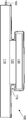
도 1은 수직 트랜지스터의 개략 단면도.
도 2 내지 도 8은 도 1에 도시된 수직 트랜지스터를 제조하는 방법의 예시적인 실시예와 연관된 프로세스 단계의 개략 단면도.
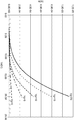
도 9는 도 1에 도시된 수직 트랜지스터를 위한 성능 전달 특성을 도시하는 그래프.
도 10은 도 1에 도시된 수직 트랜지스터를 위한 성능 Id-Vd 곡선 특성을 도시하는 그래프.1 is a schematic cross-sectional view of a vertical transistor.
2-8 are schematic cross-sectional views of process steps associated with an exemplary embodiment of a method of manufacturing the vertical transistor shown in FIG. 1.
FIG. 9 is a graph showing performance transfer characteristics for the vertical transistor shown in FIG.
FIG. 10 is a graph showing the performance I d -V d curve characteristics for the vertical transistor shown in FIG. 1. FIG.
이하에 제시된 본 발명의 바람직한 실시예의 상세한 설명에서, 첨부 도면이 참조된다.In the following detailed description of the preferred embodiments of the present invention, reference is made to the accompanying drawings.
본 설명은 본 발명에 따른 장치의 부분을 형성하는 또는 더 직접적으로 장치와 협동하는 요소에 관련될 것이다. 구체적으로 도시되거나 설명되지 않은 요소는 당 기술 분야의 숙련자들에게 잘 알려진 다양한 형태를 취할 수도 있다는 것이 이해되어야 한다.The description will relate to elements which form part of the device according to the invention or more directly cooperate with the device. It is to be understood that elements that are not specifically shown or described may take various forms that are well known to those skilled in the art.
도 1을 참조하면, 수직 트랜지스터(100)의 개략 단면도가 도시되어 있다. 트랜지스터(100)는 기판(110), (제 1) 전기 전도성 재료층(120) 및 (제 1) 전기 절연성 재료층(130)을 포함한다. 트랜지스터(100)는 다른 (제 2) 전기 절연성 재료층(150), 반도체 재료층(160), 전극(들)(700) 및 전극(800)을 또한 포함한다.Referring to FIG. 1, a schematic cross-sectional view of a
전도층(120)은 기판(110)과 절연층(130) 사이에 위치된다. 전도층(120)의 제 1 표면은 기판(110)의 제 1 표면에 접촉하고, 반면에 전도층(120)의 제 2 표면은 절연층(130)의 제 1 표면에 접촉한다. 절연성 재료층(130)은 종종 유전 재료층이라 칭한다. 종종 지지체라 칭하는 기판(110)은 강성 또는 가요성일 수 있다.The
절연층(130), 전도층(120), 기판(100) 또는 이들의 조합은 적어도 하나의 다른 층 또는 기판에 대해 적절하게 치수 설정(또는 크기 설정)되고, 위치 설정되거나 또는 치수 설정되고 위치 설정되어 트랜지스터(100) 내에 재진입 프로파일(170)을 생성한다. 이와 같이, 절연층(130), 전도층(120), 기판(100)의 하나 이상의 적어도 일부는 트랜지스터(100)의 재진입 프로파일(170)을 형성한다고 일컬어질 수 있다. 재진입 프로파일(170)은 방향성(또는 시선) 증착(또는 코팅) 프로세스를 사용하여 증착된(또는 코팅된) 재료로부터 전도층(120)의 적어도 일부를 차폐한다. 재진입 프로파일(170)은 전도층(120)의 적어도 일부가 등각(conformal) 증착(또는 코팅) 프로세스를 사용하여 증착된 재료에 액세스 가능하게 한다. 예를 들어, 전기 절연성 재료층(130) 및 전기 전도성 재료층(120)은 재진입 프로파일(170)을 형성할 수 있다.The
도 1에 도시된 바와 같이, 재진입 프로파일(170)은 전기 절연성 재료층(130) 및 전기 전도성 재료층(120) 중 하나 또는 모두의 부분에 의해 형성된다. 절연층(130)은 절연층(130)이 전도층(120)에 대해 재진입 프로파일(170)을 생성하도록 전도층(120)을 넘어 연장하도록 치수 설정되고 위치 설정된다. 달리 말하면, 전도층(120)은 전도층(120)이 절연층(130)에 대한 재진입 프로파일(170)을 생성하도록 절연층(130)이 종료하기 전에 종료되도록 크기 설정되고 위치 설정된다(도 1에 도시된 바와 같이 좌측 및 우측 방향의 모두에서).As shown in FIG. 1, the
절연성 재료층(150)은 트랜지스터(100)의 재진입 프로파일(170)에 합치한다. 절연성 재료층(150)은 제 1 및 제 2 표면을 포함하고, 제 1 표면은 절연층(130), 전도층(120) 및 기판(110)의 표면의 부분과 접촉한다. 반도체 재료층(160)은 트랜지스터(100)의 재진입 프로파일(170)에 합치한다. 반도체층(160)은 제 1 및 제 2 표면을 포함하고, 제 1 표면은 절연층(150)의 제 2 표면과 접촉한다. 반도체층(160)의 제 2 표면의 별개의(또는 개별, 상이한) 부분은 전극(들)(700) 및 전극(800)과 접촉한다.
전극(들)(700)은 다른 (제 2) 전기 전도성 재료층(710)을 포함한다. 전극(800)은 또 다른 (제 3) 전기 전도성 재료층(810)을 포함한다. 전극(들)(700) 및 전극(800)은 트랜지스터(100)의 상이한 위치에서 서로로부터 이격되어 위치된다. 제 2 및 제 3 전기 전도성 재료층(710, 810)은 동일한 재료층일 수 있다. 이러한 것이 행해질 때, 전극(들)(700) 및 전극(800)은 동일한 전기 전도성 재료층, 재료층(710) 또는 재료층(810)의 별개의 부분 내에 포함된다. 대안적으로, 제 2 및 제 3 전기 전도성 재료층(710, 810)은 별개의(상이한) 재료층일 수 있다.Electrode (s) 700 include another (second) electrically
전도층(120)은 트랜지스터(100)의 게이트로서 기능한다. 트랜지스터(100)의 몇몇 예시적인 실시예에서, 전극(들)(700)은 트랜지스터(100)의 드레인으로서 기능하고, 전극(800)은 트랜지스터(100)의 소스로서 기능한다. 트랜지스터(100)의 다른 예시적인 실시예에서, 전극(들)(700)은 소스로서 기능하고 전극(800)은 드레인으로서 기능한다.
반도체 디바이스는 이하의 방식으로 작동된다. 트랜지스터(100)가 제공된 후에, 전압이 제 2 전기 전도성 재료층(710)과 제 3 전기 전도성 재료층(810) 사이에 인가된다. 전압이 또한 제 1 전기 전도성 재료층(120)에 인가되어 제 2 전기 전도성 재료층(710) 및 제 3 전기 전도성 재료층(810)을 전기적으로 접속한다.The semiconductor device is operated in the following manner. After the
트랜지스터(100)의 재진입 프로파일(170)은 트랜지스터의 반도체 재료 채널의 치수가 트랜지스터(100)의 게이트로서 기능하는 전도층(120)의 두께와 연관될 수 있게 한다. 유리하게는, 본 발명의 이 아키텍처는 소형 채널을 포함하는 트랜지스터의 제조 중에 고분해능 또는 매우 미세한 정렬 특징에 대한 의존성을 감소시킨다.
도 2 내지 도 8을 참조하면, 트랜지스터(100)를 제조하는 방법의 예시적인 실시예와 연관된 프로세스 단계의 개략 단면도가 도시되어 있다.2-8, a schematic cross-sectional view of process steps associated with an exemplary embodiment of a method of fabricating
일반적으로 설명하면, 트랜지스터(100)는 이하의 방식으로 제조된다. 기판(110)이 전기 전도성 재료층(120) 및 전기 절연성 재료층(130)을 순서대로 포함하여 제공된다. 레지스트 재료층(140)이 전기 절연성 재료층(130) 위에 있다. 레지스트 재료층(140)은 전기 절연성 재료층(130)의 부분을 노출시키도록 패터닝된다. 전기 절연성 재료층(130)의 노출된 부분은 전기 전도성 재료층(120)의 부분을 노출시키도록 제거된다. 전기 전도성 재료층(120)의 노출된 부분은 제거된다. 전도성 재료층(120)의 제거는 재진입 프로파일(170)을 생성하도록 계속된다. 도 1에 도시된 바와 같이, 재진입 프로파일(170)은 전기 전도성 재료층(120)의 일부의 제거에 의해 생성되고, 반면에 전기 절연성 재료층(130)의 일부는 잔류한다. 이 개념에서, 재진입 프로파일(170)은 전기 절연성 재료층(130)에 대해 전도성 재료층(120) 내에 생성된다고 일컬어질 수 있다. 포토레지스트층(140)의 제거 후에, 이러한 것이 필요하면, 기판(110) 및 잔여 노출된 재료층(120, 130)은 제 2 전기 절연성 재료층(150)으로 등각 코팅된다. 제 2 절연성 재료층(150)은 반도체 재료층(160)으로 등각 코팅된다. 전기 전도성 재료층(710 또는 810) 또는 층(710, 810)은 반도체 재료층(160) 위에 방향성 증착된다.Generally speaking,
레지스트 재료층(140)은 전기 절연성 재료층(130) 위에 증착되고 동일한 프로세스 단계에서 패터닝될 수 있다. 액체 에칭제는 전기 절연성 재료층(130)의 노출된 부분을 제거하여 전기 전도성 재료층(120)의 부분을 노출시키는데 사용될 수 있다. 전기 절연성 재료층(130)의 노출된 부분을 제거하는데 사용되는 동일한 액체 에칭제가 전기 전도성 재료층(120)의 노출된 부분을 제거하여 전기 전도성 재료층(120) 내에 재진입 프로파일(170)을 생성하는데 사용될 수 있다.Resist
몇몇 예시적인 실시예에서, 기판(110)은 하나 초과의 재료층을 포함할 수 있다. 부가의 재료층(들)이 몇몇 예에서 제조 프로세스 중에 기판(110)의 구조적 완전성을 향상시키거나 유지시키기 위해 포함된다. 기판(110)이 하나 초과의 재료층, 예를 들어 제 1 층 및 제 2 층을 포함할 때, 제조 방법은 기판(110)의 제 2 층을 제거하는 단계를 포함할 수 있다.In some demonstrative embodiments,
도 2를 재차 참조하면, 재료 프로세싱 이전의 트랜지스터(100) 재료층의 개략 단면도가 도시된다. 수직 트랜지스터 디바이스를 형성하기 위한 제조 프로세스는 전도층(120)에 인접한 기판의 적어도 일부[도 2에 도시된 바와 같이 기판(110)의 상부]에 대해 전체적으로 또는 부분적으로 비전도성인 기판(110)에서 시작하여, 트랜지스터(100)의 전기 단락이 발생하지 않게 된다. 전도층(120)은 기판(110)에 도포되거나 기판(110) 상에 증착된다. 전도층(200)은 트랜지스터(100)의 게이트로서 기능하고, 그 두께에 의해(도 2에 도시된 바와 같이 수직 방향에서) 그 두께만큼 게이트의 길이를 규정한다. 유전성 비전도층(130)이 전도층(120)에 도포되거나 그 위에 코팅된다. 비전도층(130)은 패턴을 갖지 않는 균일한 층이다. 레지스트층(140)은 유전성 비전도층(130)에 도포된다. 레지스트(400)는 패터닝된다.Referring again to FIG. 2, a schematic cross-sectional view of a
기판(110)은 임의의 층 또는 프로세싱 방법과 상당히 상호 작용하지 않는다. 종종 지지체라 칭하는 기판(110)은 제조, 시험 및/또는 사용 중에 박막 트랜지스터(또한 TFT라 칭함)를 지지하기 위해 사용될 수 있다. 당 기술 분야의 숙련자들은 상업적 실시예를 위해 선택된 지지체가 시험 또는 스크리닝 실시예를 위해 선택된 것과 상이할 수 있다는 것을 이해할 수 있을 것이다. 몇몇 실시예에서, 기판(110)은 TFT를 위한 임의의 필수 전기 기능을 제공하지 않는다. 이 유형의 기판(110)은 본 명세서에서 "비참여 지지체"라 명명한다. 유용한 기판 재료는 유기 또는 무기 재료를 포함한다. 예를 들어, 기판(110)은 무기 글래스, 세라믹 포일, 폴리머 재료, 충전된 폴리머 재료, 코팅된 금속 포일, 아크릴, 에폭시, 폴리아미드, 폴리카보네이트, 폴리이미드, 폴리케톤, 폴리(옥시-1,4-페닐렌옥시-1,4-페닐렌카르복실-1,4-페닐렌)(종종 폴리(에테르 에테르 케톤) 또는 PEEK라 칭함), 폴리노르보넨, 폴리페닐렌옥사이드, 폴리(에틸렌 나프탈렌디카르복실레이트)(PEN), 폴리(에틸렌 테레프탈레이트)(PET), 폴리(에테르 설폰)(PES), 폴리(페닐렌 설파이드)(PPS) 및 파이버 보강 플라스틱(FRP)을 포함할 수 있다. 기판(110)의 두께는 다양할 수 있는데, 통상적으로 약 100 ㎛ 내지 약 1 cm이다.
가요성 지지체 또는 기판(110)이 본 발명의 몇몇 예시적인 실시예에서 사용된다. 가요성 기판(110)을 사용하는 것은 연속적일 수 있는 롤 프로세싱을 허용하여, 편평한 또는 강성 지지체 위의 경제적인 제조 및 경제적인 스케일을 제공한다. 선택된 가요성 지지체는 도움을 받지 않은 손에 의한 것과 같은 적은 힘을 사용하여 왜곡 또는 파괴 없이, 바람직하게는 약 50 cm 미만의 직경, 더 바람직하게는 25 cm의 직경, 가장 바람직하게는 10 cm의 직경의 실린더의 원주 주위에 감겨지는 것이 가능하다. 바람직한 가요성 지지체는 자체로 롤링될 수 있다. 가요성 기판의 부가의 예는 박막 트랜지스터를 전기적으로 절연하기 위해 절연층으로 코팅된 포일이 제공된 스테인레스강과 같은 박막 금속 포일을 포함한다. 가요성이 고려되지 않는다면, 기판은 글래스 및 실리콘을 포함하는 재료로 제조된 웨이퍼 또는 시트일 수 있다.Flexible support or
몇몇 예시적인 실시예에서, 기판(110)은 예를 들어 부가의 구조적 지지체가 일시적인 목적으로, 예를 들어 제조, 운반, 시험 또는 저장을 위해 요구될 때 일시적 지지체 또는 지지층을 포함할 수 있다. 이들 예시적인 실시예에서, 기판(110)은 일시적인 지지체에 탈착 가능하게 부착되거나 기계적으로 고착될 수 있다. 예를 들어, 가요성 폴리머 지지체는 트랜지스터 제조 프로세스 중에 부가의 구조적 강성을 제공하기 위해 강성 글래스 지지체에 일시적으로 부착될 수 있다. 글래스 지지체는 제조 프로세스의 완료 후에 가요성 폴리머 지지체로부터 제거될 수 있다.In some demonstrative embodiments,
통상적으로 전도체라 칭하는 전도층(120)은 전도층(120)이 게이트로서 기능하게 허용하는 임의의 적합한 전도성 재료일 수 있다. 변성 도핑된 반도체, 전도성 폴리머 및 카본 잉크와 같은 인쇄 가능한 재료, 은-에폭시 또는 소결 가능한 금속 나노입자 현탁액을 포함하는 당 기술 분야에 공지된 다양한 게이트 재료가 또한 적합하다. 예를 들어, 게이트 전극은 도핑된 실리콘, 또는 알루미늄, 크롬, 금, 은, 니켈, 구리, 텅스텐, 팔라듐, 플래티늄, 탄탈 및 티타늄과 같은 금속을 포함할 수 있다. 게이트 전극 재료는 또한 인듐-주석 산화물(ITO), ZnO, SnO2 또는 In2O3와 같은 투명한 전도체를 포함할 수 있다. 예를 들어 폴리아닐린, 폴리(3,4-에틸렌디옥시티오펜)/폴리(스티렌 설포네이트)(PEDOT:PSS)와 같은 전도성 폴리머가 또한 사용될 수 있다. 게다가, 이들 재료의 합금, 조합 및 다층이 사용될 수 있다.
게이트 전극은 화학 기상 증착, 스퍼터링, 증착, 도핑 또는 용액 프로세싱을 사용하여 기판(110) 상에 증착될 수 있다. 본 발명의 몇몇 실시예에서, 동일한 재료가 게이트 전극 기능을 제공할 수 있고 또한 기판(110)이 또한 트랜지스터(100)를 전기적으로 절연하기 위한 절연층을 포함하면 기판(110)의 지지 기능을 제공할 수 있다. 예를 들어, 도핑된 실리콘은 게이트 전극으로서 기능할 수 있고 TFT를 지지할 수 있다.The gate electrode may be deposited on the
게이트 전극의 두께(도 2에 도시된 바와 같이 수직 방향)는 다양할 수 있는데, 통상적으로 약 100 내지 약 10000 nm이다. 두께가 게이트 길이를 규정하기 때문에, 두께는 일반적으로 전기 단락의 가능성을 감소시키기 위해 등각 코팅된 재료의 두께의 2배보다 두껍다.The thickness of the gate electrode (vertical direction as shown in FIG. 2) may vary, typically from about 100 to about 10000 nm. Since the thickness defines the gate length, the thickness is generally thicker than twice the thickness of the conformal coated material to reduce the possibility of electrical shorts.
도 2에 도시된 바와 같이, 비전도층(130)은 전도층(120) 위에 균일하게 코팅된다. 비전도층(130)에 사용을 위해 적합한 예시적인 재료는 스트론시에이트, 탄탈레이트, 티타네이트, 지르코네이트, 산화알루미늄, 산화실리콘, 산화탄탈, 산화티타늄, 실리콘 니트라이드, 바륨 티타네이트, 바륨 스트론튬 티타네이트, 바륨 지르코네이트 티타네이트, 아연 셀레나이드 및 아연 설파이드를 포함한다. 게다가, 이들 예의 합금, 조합 및 다층이 통상적으로 게이트 유전체라 칭하는 비전도층(130)을 위해 사용될 수 있다. 이들 재료들 중에서, 산화알루미늄, 산화실리콘 및 아연 셀레나이드가 바람직하다. 게다가, 폴리이미드, 폴리비닐 알코올, 폴리(4-비닐페놀), 폴리이미드 및 폴리(비닐리덴 플루오라이드), 폴리스티렌 및 그 치환된 유도체, 폴리(비닐 나프탈렌) 및 치환된 유도체 및 폴리(메틸 메타크릴레이트)와 같은 폴리머가 사용될 수 있다.As shown in FIG. 2, the
비전도층(130)은 레지스트(400)로 코팅된다. 레지스트(400)는 패터닝된다. 레지스트(400)는 폴리머 포지티브 작용 레지스트 또는 네거티브 레지스트와 같은 당 기술 분야에 공지된 통상의 포토레지스트일 수 있다. 레지스트(400)는 적은 분해능(> 1 mm) 정렬을 갖고 마스크를 통해 기판(110)에 노출되고 현상되어 레지스트의 패턴을 생성한다. 다른 예시적인 실시예에서, 레지스트(400)의 패턴은 마스크를 사용하지 않고 패터닝된 방식으로 직접 레지스트를 인쇄하는 플렉소그래피 또는 잉크젯 인쇄와 같은 인쇄 프로세스를 사용하여 성취된다.The
도 3 내지 도 5를 재차 참조하면, 재료 프로세싱 중 및 후에 트랜지스터(100) 재료층의 개략 단면도가 도시된다. 도 3에서, 통상적으로 비전도체라 칭하는 비전도층(130)이 패터닝된 레지스터(400)를 통해 에칭된다. 에칭제는 레지스트(400) 또는 기초 전도체층(120)을 실질적으로 공격하지 않고 비전도성 재료를 제거하는 임의의 유기 또는 무기 재료일 수 있다. 전도체(120)는 이어서 전도체(120)를 제거하는 적합한 에칭제를 사용하여 제거되지만, 기판(110) 또는 기초 비전도체(130)에 거의 영향을 미치지 않는다. 이와 같이, 선택된 에칭제는 종종 기판(110), 전도체(120) 또는 비전도체(130)에 의존한다. 이 시점에 레지스트(140)와의 에칭제 상호 작용 및 레지스트(140)의 손실은 일반적으로 적은 결과를 갖는데, 이는 비전도체(130)가 이제 마스크로서 작용하기 때문이다. 도 3에 도시된 바와 같이, 에칭 프로세스 또는 프로세스들은 전도체(120) 및 비전도체(130)의 부분을 에칭 제거하여 전도체(120) 및 비전도체(130)가 동일한 패턴을 갖게 된다.Referring again to FIGS. 3-5, schematic cross-sectional views of the
도 4에 도시된 바와 같이, 전도체(120)의 선택적 에칭은 도 4에 도시된 재진입 프로파일(170)이 형성될 때까지 계속된다. 전도체(120)의 에칭이 완료될 때, 비전도체(130)는 전도체(120)보다 돌출되어 기판(110) 위에 위치된(도 4에 도시된 바와 같이) 방향성(또는 시선) 코팅 소스에 의해 코팅으로부터 기초 표면[또는 전도체(120) 또는 기판(110)의]의 적어도 일부를 차폐하는데 충분한 재진입 프로파일(170)을 생성한다. 달리 말하면, 전도체(120)는 비전도체(130)보다 움푹 들어간다. 잔여 전도체(120)는 반도체 디바이스가 완성될 때 게이트 전도체로서 작용한다.As shown in FIG. 4, selective etching of the
이 시점에서, 필요하다면, 레지스트(140)가 제거된다. 세척 프로세스가 재진입 프로파일(170)을 제거하지 않으면, 원한다면 온건한 세척이 재료층 스택 상에 수행될 수 있다. 도 5는 재진입 프로파일(170)이 생성된 후에 그리고 레지스트가 제거된 후에 반도체 디바이스의 단면도를 도시한다.At this point, if necessary, the resist 140 is removed. If the cleaning process does not remove the
도 6 및 도 7을 재차 참조하면, 종종 절연체라 칭하는 유전성 비전도성 재료 및 반도체 재료의 등각 코팅 후의 반도체 디바이스의 개략 단면도가 도시되어 있다. 도 6에서, 유전성 비전도성 재료(150)가 이어서 기판(110) 및 재료층(120, 130)에 의해 형성된 토포그래픽 특징부 위에 등각 코팅 증착 프로세스를 사용하여 등각 코팅된다. 등각 코팅 프로세스를 사용하여 비전도성 재료(150)를 도포하는 것은 재진입 프로파일(170)을 유지하는 것을 돕는다. 비전도성 재료(150)는 종종 게이트 유전체라 칭한다. 적합한 비전도성 재료는 스트론시에이트, 탄탈레이트, 티타네이트, 지르코네이트, 산화알루미늄, 산화실리콘, 산화탄탈, 산화티타늄, 실리콘 니트라이드, 바륨 티타네이트, 바륨 스트론튬 티타네이트, 바륨 지르코네이트 티타네이트를 포함한다. 유전성 재료는 도포될 반도체 재료로부터 게이트 전도체를 분리하기 때문에, 등각 코팅된 재료가 적어도 재진입 프로파일(170) 및 게이트가 위치되는 영역에서 일정한 또는 균일한 두께를 구비하는 것이 중요하다.Referring again to FIGS. 6 and 7, a schematic cross-sectional view of a semiconductor device after conformal coating of a dielectric material and a dielectric nonconductive material, often referred to as an insulator, is shown. In FIG. 6, dielectric
등각 코팅을 성취하기 위한 바람직한 프로세스는 이들 프로세스가 고도로 다양한 토폴로지 위에 또는 상에 균일한 두께를 생성하기 때문에 원자층 증착(ALD) 또는 공간 ALD(S-ALD) 또는 플라즈마 향상 ALD(PEALD)와 같은 그 변형 중 하나를 포함한다. ALD 및 S-ALD는 이하에 더 상세히 설명된다.Preferred processes for achieving conformal coatings are those such as atomic layer deposition (ALD) or spatial ALD (S-ALD) or plasma enhanced ALD (PEALD) because these processes produce a uniform thickness over or on a wide variety of topologies. One of the variations. ALD and S-ALD are described in more detail below.
도 7에서, 반도체 재료(160)는 이어서 등각 코팅 증착 프로세스를 사용하여 코팅되고, 이 프로세스는 재진입 프로파일(170)을 유지하는 것을 돕는다. 이 등각 코팅 프로세스는 유전성 재료를 코팅하기 위해 이전에 사용된 동일한 프로세스일 수 있다. 대안적으로, 등각 코팅 프로세스는 상이할 수 있다. 반도체 재료(160)는 게이트(120)가 여기될 때 전극(700, 800) 사이의 채널로서 작용하기 때문에, 등각 코팅된 재료는 적어도 재진입 프로파일(170) 및 게이트가 위치되는 영역에서 그리고 더 바람직하게는 재진입 프로파일(170) 및 게이트가 위치되어 있는 영역을 포함하는 전극(들)(700)과 전극(800) 사이의 영역에서 일정한 또는 균일한 두께를 구비하는 것이 중요하다. 등각 코팅을 위한 바람직한 프로세스는 원자층 증착(ALD) 또는 공간 ALD(S-ALD)와 같은 그 다양한 변형 중 하나이다. 이 프로세스는 고도로 다양한 토폴로지에 균일한 두께를 생성한다. ALD 및 S-ALD는 이하에 더 상세히 설명된다.In FIG. 7,
종종 반도체라 칭하는 반도체 재료층(160)은, 반도체 재료가 ALD와 같은 등각 코팅 프로세스를 사용하여 증착되거나 코팅될 수 있으면 임의의 유형의 반도체일 수 있다. 적합한 반도체 재료의 예는 산화아연, 아연 칼코게나이드, 카드뮴 칼코게나이드, 갈륨 프닉타이드, 알루미늄 닉타이드 또는 실리콘을 포함한다.The
반도체는 전도도를 증가시키거나 감소시키기 위해 다른 재료로 선택적으로 도핑될 수 있다. 몇몇 예시적인 실시예에서, 고갈 모드 디바이스가 바람직하고, 따라서 캐리어는 도펀트의 사용을 통해 첨가될 수 있다. 반도체가 산화아연일 때, 알루미늄 도펀트의 사용은 예를 들어 전자 캐리어 밀도를 증가시킨다. 이 구성에서, 게이트는 통상적으로 드레인 및 소스에 대해 이를 네거티브가 되게 함으로써 디바이스를 턴오프하는데 사용된다.The semiconductor may be selectively doped with other materials to increase or decrease the conductivity. In some demonstrative embodiments, depletion mode devices are preferred, and thus carriers may be added through the use of dopants. When the semiconductor is zinc oxide, the use of aluminum dopants increases the electron carrier density, for example. In this configuration, the gate is typically used to turn off the device by making it negative for drain and source.
보상 도펀트가 또한 진성 캐리어 밀도를 고갈하는데 사용될 수 있다. 반도체가 산화아연일 때, 질소의 사용은 전자 캐리어 밀도를 감소시켜 이를 덜 n-형이 되게 하는 것으로 판명되었다. 이 구성에서, 반도체는 포지티브 게이트 전압이 인가될 때 트랜지스터를 턴온하기 위해 축적 모드에서 작동하도록 제조될 수 있다. 이들 도펀트는 성장 프로세스 중에 화합물로서 종종 첨가되지만, 반도체층이 이온 주입 및 열 확산과 같은 프로세스를 사용하여 도포된 후에 또한 첨가될 수 있다.Compensation dopants can also be used to deplete intrinsic carrier density. When the semiconductor is zinc oxide, the use of nitrogen has been found to reduce the electron carrier density, making it less n-type. In this configuration, the semiconductor can be fabricated to operate in accumulation mode to turn on the transistor when a positive gate voltage is applied. These dopants are often added as compounds during the growth process, but may also be added after the semiconductor layer has been applied using processes such as ion implantation and thermal diffusion.
도 8을 재차 참조하면, 전기 전도성 재료의 방향성 코팅 중에 반도체 디바이스의 개략 단면도가 도시되어 있다. 반도체층(160)이 증착된 후에, 소스 및 드레인 전극(들)(700) 및 전극(800)이 방향성(시선) 증착 프로세스를 사용하여 증착되고 이 프로세스는 재진입 프로파일(170) 내로 재료를 증착하거나 코팅하지 않는다. 적합한 방향성 증착 프로세스의 예는 열 증착, 전자 빔 증착, 스퍼터링 또는 레이저 융삭을 포함한다. 전극(들)(700)과 전극(800) 사이의 능동 채널 간극이 전도성 재료층(120)에 대한 비전도층(130)의 돌출에 의해 캐스팅된 섀도우에 의해 유지된다.Referring again to FIG. 8, a schematic cross-sectional view of a semiconductor device is shown during a directional coating of an electrically conductive material. After the
도 1을 재차 참조하면, 전극(들)(700) 및 전극(800)이 증착된 후에 트랜지스터(100)가 도시되어 있다. 트랜지스터(100)의 드레인 및 소스는 전극(700) 및 전극(800)으로부터 선택될 수 있고, 선택은 통상적으로 고려된 디바이스의 용례 및 특성에 기초한다. 도 1에 도시된 바와 같이, 전극(800)이 비전도체(130) 및 전도체(120)에 의해 형성된 메사의 상부에 위치되고, 전극(들)(700)은 그렇지 않다. 이와 같이, 전극(700) 및 전극(800)은 상이한 평면 상에 있다. 임의의 필요한 상호 접속이 예를 들어 당 기술 분야에 잘 알려진 층 평탄화 및 비아 피드스루와 같은 통상의 기술을 사용하여 성취될 수 있다.Referring again to FIG. 1,
기판(110), 전도층(120), 비전도층(130), 비전도층(150), 반도체층(160) 또는 이들의 조합은 층의 기능적 양태가 불변 유지되면 하나 이상의 층을 포함할 수 있다. 전술된 층의 기능이 보존되는 한, 부가의 층, 예를 들어 평탄화층, 배리어층, 접착층이 반도체 디바이스 내에 포함될 수 있다.
원자층 증착(ALD)은 일정하고, 균일한 또는 심지어 정확한 것으로 고려될 수 있는 두께를 갖는 코팅을 생성하는데 사용되는 프로세스이다. ALD는 등각 또는 심지어 고도의 등각 재료층으로 고려될 수 있는 코팅을 생성한다. 일반적으로 설명하면, ALD 프로세스는 진공 챔버 내에 통상적으로 전구체라 칭하는 2개 이상의 반응 재료 사이에서 교대함으로써 기판 코팅을 성취한다. 제 1 전구체가 인가되어 기판과 반응한다. 과잉의 제 1 전구체가 진공 챔버로부터 제거된다. 제 2 전구체가 이어서 인가되어 기판과 반응한다. 과잉의 제 2 전구체는 진공 챔버로부터 제거되고 프로세스가 반복된다.Atomic layer deposition (ALD) is a process used to create a coating having a thickness that can be considered to be constant, uniform or even accurate. ALD produces a coating that can be considered a conformal or even highly conformal material layer. Generally described, the ALD process achieves substrate coating by alternating between two or more reactive materials, commonly referred to as precursors, in a vacuum chamber. A first precursor is applied to react with the substrate. Excess first precursor is removed from the vacuum chamber. A second precursor is then applied to react with the substrate. Excess second precursor is removed from the vacuum chamber and the process is repeated.
최근에, 진공 챔버의 필요성을 무효화하는 신규한 ALD 프로세스가 개발되었다. 통상적으로 S-ALD라 칭하는 이 프로세스는 미국 특허 제 7,413,982호, 미국 특허 제 7,456,429호, 미국 특허 공개 제 2008/0166884호 및 미국 특허 공개 제 2009/0130858호에 설명되어 있고, 이들의 개시 내용은 본 명세서에 참조로서 포함되어 있다. S-ALD는 일정하고, 균일한 또는 심지어 정확한 것으로 고려될 수 있는 두께를 갖는 코팅을 생성한다. S-ALD는 등각 또는 심지어 고도의 등각 재료층으로 고려될 수 있는 코팅을 생성한다. S-ALD는 저온 코팅 환경과 적합성이 있고 다른 코팅 기술에 비교할 때 더 높은 이동도 재료를 사용하는 능력을 제공한다. 부가적으로, S-ALD는 웨브 코팅과 적합성이 있어, 대량 생산 작업을 위해 매력적이게 한다. 몇몇 웨브 코팅 작업은 정렬 문제점, 예를 들어 웨브 트래킹 또는 신장 문제점을 경험할 수도 있지만, 본 발명의 아키텍처는 제조 프로세스 중에 높은 분해능 또는 매우 미세한 정렬 특징에 대한 의존성을 감소시킨다. 이와 같이, S-ALD는 본 발명의 제조에 양호하게 적합된다.
Recently, new ALD processes have been developed that negate the need for vacuum chambers. This process, commonly referred to as S-ALD, is described in US Pat. No. 7,413,982, US Pat. No. 7,456,429, US Patent Publication 2008/0166884 and US Patent Publication 2009/0130858, the disclosures of which are disclosed herein. It is incorporated by reference in the specification. S-ALD produces a coating having a thickness that can be considered to be constant, uniform or even accurate. S-ALD produces coatings that can be considered as conformal or even highly conformal material layers. S-ALD is compatible with low temperature coating environments and offers the ability to use higher mobility materials when compared to other coating technologies. In addition, S-ALD is compatible with web coatings, making it attractive for mass production operations. Some web coating operations may experience alignment problems, such as web tracking or stretching problems, but the architecture of the present invention reduces the dependence on high resolution or very fine alignment features during the manufacturing process. As such, S-ALD is well suited to the manufacture of the present invention.
실험 결과Experiment result
600 nm 크롬층이 열적 산화물층에 의해 코팅된 62.5 mm 정사각형 실리콘 기판 상에 스퍼터링을 경유하여 증착되었다. 이 상부에는, 120 nm 알루미늄 산화물층이 미국 특허 제 7,413,982호에 설명된 S-ALD 프로세스 및 질소의 불활성 캐리어 가스를 갖는 물 및 유기 금속 전구체 트리메틸 알루미늄을 갖는 미국 특허 제 7,456,429호에 설명된 S-ALD 장치를 사용하여 섭씨 200도에서 코팅되었다.A 600 nm chromium layer was deposited via sputtering on a 62.5 mm square silicon substrate coated with a thermal oxide layer. On top of this, a 120 nm aluminum oxide layer has a S-ALD process described in US Pat. No. 7,413,982 and S-ALD described in US Pat. No. 7,456,429 with organometallic precursor trimethyl aluminum with water with an inert carrier gas of nitrogen. It was coated at 200 degrees Celsius using the device.
포토레지스트의 패터닝된 층이 섭씨 115도에서 60초 동안 고온 플레이트 상에 배치된 1000 rpm Microposit S1805 레지스트[미국 말보로 소재의 롬 앤 하스 일렉트로닉 머트리얼즈 엘엘씨(Rohm and Haas Electronic Materials LLC)]에서 스핀 코팅에 의해 형성되었고, 이어서 저분해능 또는 조잡한 정렬로서 실리콘 기판의 에지만을 사용하여 Cobilt 마스크 정렬기[미국 캘리포니아주 서니베일 소재의 컴퓨터비전 코포레이션(Computervision Corporation)으로부터의 Cobilt 모델 CA-419] 상에 70초 동안 라인을 포함하는 글래스/크롬 접촉 마스크를 통해 노출되었다. 샘플은 이어서 Microposit MF-319 현상제(미국 말보로 소재의 롬 앤 하스 일렉트로닉 머트리얼즈 엘엘씨) 내에서 60초 동안 현상되었고, DI 수 내에서 5분 동안 헹굼되었다.The patterned layer of photoresist spins on a 1000 rpm Microposit S1805 resist (Rohm and Haas Electronic Materials LLC, Marlboro, USA) placed on a hot plate for 60 seconds at 115 degrees Celsius. 70 formed on a Cobilt mask aligner (Cobilt Model CA-419 from Computervision Corporation, Sunnyvale, Calif.) Using only the edges of the silicon substrate as a low resolution or coarse alignment. It was exposed through a glass / chrome contact mask containing lines for seconds. The sample was then developed for 60 seconds in the Microposit MF-319 developer (Rom & Haas Electronic Materials LLC, Marlborough, USA) and rinsed for 5 minutes in DI water.
비전도성 알루미늄 산화물이 6.5분 동안 농축된 인산으로 섭씨 60도에서 에칭되었다. 크롬은 8% 아세트산으로 세륨 염화암모늄의 0.6 M 용액을 포함하는 크롬 에치를 사용하여 에칭되었다. 노출된 크롬은 13.3분 내에 가시적으로 에칭되었다. 언더컷 에칭이 2분의 계속된 에칭을 경유하여 성취되었다. 기판은 이어서 5분 동안 DI 수 내에서 헹굼되었고, 포토레지스트를 제거하기 위해 아세톤으로 헹굼되었고, 이어서 HPLC 등급 이소프로판올 내에서 헹굼되었고, 이어서 건조되었다.Non-conductive aluminum oxide was etched at 60 degrees Celsius with concentrated phosphoric acid for 6.5 minutes. Chromium was etched using chromium etch containing a 0.6 M solution of cerium ammonium chloride with 8% acetic acid. The exposed chromium was visually etched in 13.3 minutes. Undercut etching was achieved via two minutes of continued etching. The substrate was then rinsed in DI water for 5 minutes, rinsed with acetone to remove the photoresist, and then rinsed in HPLC grade isopropanol and then dried.
기판은 이어서 S-ALD 장치 및 프로세스를 사용하여 등각으로 120 nm 두께의 알루미늄 산화물의 부가의 층으로 전술된 바와 같이 코팅되었다. 기판은 이어서 전구체 디에틸 아연을 사용하여 250 nm의 아연 산화물 층으로 코팅되었고 암모니아 용액 및 캐리어 가스로서 질소로 농축되었다.The substrate was then coated as described above with an additional layer of 120 nm thick aluminum oxide conformally using S-ALD apparatus and process. The substrate was then coated with a 250 nm zinc oxide layer using precursor diethyl zinc and concentrated with nitrogen as ammonia solution and carrier gas.
전극은 증착에 의해 도포되었다. 알루미늄은 기판 상의 각각의 라인을 가로질러 완전히 수직으로 연장하는 정사각형 구멍을 포함하는 섀도우 마스크를 통해 증착되었다. 알루미늄은 70 nm 두께였다.The electrode was applied by vapor deposition. Aluminum was deposited through a shadow mask comprising square holes extending completely vertically across each line on the substrate. Aluminum was 70 nm thick.
트랜지스터의 시험은 라인의 상부의 알루미늄, 라인의 일 측면의 알루미늄 및 게이트로서 작용하는 크롬 게이트 금속에 접촉하기 위해 프로브 스테이션을 사용함으로써 성취되었다. 도 9를 참조하면, 트랜지스터를 위한 성능 전달 특성을 도시하는 그래프가 도시되어 있다. 도 9에서 볼 수 있는 바와 같이, 드레인 전류 대 게이트 전압은 20 볼트의 드레인 전압에서 일정하다. 모든 게이트 전압에서 매우 적은 누설을 갖는 게이트 전류가 또한 도시되어 있다. 드레인 전류는 게이트 전압에 양호하게 응답하고, -2 볼트의 게이트에서 약 10-11 amp의 작은 전류로부터 10 볼트의 게이트에서 거의 밀리암페어의 범위이다. 도 10을 참조하면, 트랜지스터를 위한 성능 Id-Vd 곡선 특성을 도시하는 그래프가 도시되어 있다. 도 10에서 볼 수 있는 바와 같이, 드레인 전류 대 드레인 전압은 게이트 전압에 매우 응답성이다. 디바이스의 시험 결과는 또한 20 V의 드레인 전압 및 10 V의 게이트 전압에 대해 107 초과의 상당한 온/오프를 또한 나타낸다.
Testing of the transistor was accomplished by using a probe station to contact aluminum on top of the line, aluminum on one side of the line, and chromium gate metal acting as a gate. Referring to FIG. 9, there is shown a graph illustrating performance transfer characteristics for a transistor. As can be seen in Figure 9, the drain current versus gate voltage is constant at a drain voltage of 20 volts. Gate currents with very little leakage at all gate voltages are also shown. The drain current responds well to the gate voltage and ranges from a small current of about 10 -11 amps at a gate of -2 volts to almost a milliampere at a gate of 10 volts. Referring to FIG. 10, a graph showing the performance I d -V d curve characteristics for a transistor is shown. As can be seen in FIG. 10, the drain current versus drain voltage is very responsive to the gate voltage. The test results of the device also show significant on / off greater than 10 7 for a drain voltage of 20V and a gate voltage of 10V.
100: 트랜지스터 110: 기판
120: 전도체 130: 비전도체
140: 레지스트 150: 게이트 유전체
160: 반도체 170: 재진입 프로파일
700: 전극 710: 제 2 전기 전도성 재료층
800: 전극 810: 제 3 전기 전도성 재료층100: transistor 110: substrate
120: conductor 130: non-conductor
140: resist 150: gate dielectric
160: semiconductor 170: re-entry profile
700: electrode 710: second electrically conductive material layer
800: electrode 810: third layer of electrically conductive material
Claims (5)
전기 전도성 재료층 및 전기 절연성 재료층을 순서대로 포함하는 기판을 제공하는 단계와,
상기 전기 절연성 재료층 위에 레지스트 재료층을 증착하는 단계와,
상기 전기 절연성 재료층의 일부분을 노출하도록 상기 레지스트 재료층을 패터닝하는 단계와,
상기 노출된 전기 절연성 재료층을 제거하여 상기 전기 전도성 재료층의 일부분을 노출하는 단계와,
상기 노출된 전기 전도성 재료층을 제거하여 상기 전기 전도성 재료층 및 상기 전기 절연성 재료층 내에 재진입 프로파일(a reentrant profile)을 생성하는 단계와,
상기 기판 및 상기 노출된 재료층들을 제 2 전기 절연성 재료층으로 등각 코팅하는 단계와,
상기 제 2 전기 절연성 재료층을 반도체 재료층으로 등각 코팅하는 단계와,
상기 반도체 재료층 위에 전기 전도성 재료층을 방향성 증착하는 단계를 포함하는
트랜지스터 제조 방법.
In the transistor manufacturing method,
Providing a substrate comprising an electrically conductive material layer and an electrically insulating material layer in order;
Depositing a layer of resist material over the layer of electrically insulating material;
Patterning the resist material layer to expose a portion of the electrically insulating material layer;
Removing the exposed layer of electrically insulating material to expose a portion of the layer of electrically conductive material;
Removing the exposed electrically conductive material layer to create a reentrant profile in the electrically conductive material layer and the electrically insulating material layer;
Conformal coating the substrate and the exposed material layers with a second electrically insulating material layer;
Conformally coating the second electrically insulating material layer with a semiconductor material layer;
Directionally depositing an electrically conductive material layer over the semiconductor material layer.
Transistor manufacturing method.
상기 전기 절연성 재료층 위에 레지스트 재료층을 증착하는 단계 및 상기 레지스트 재료층을 패터닝하는 단계는 동일한 프로세스 단계에서 발생하는
트랜지스터 제조 방법.
The method of claim 1,
Depositing a layer of resist material over the electrically insulating material layer and patterning the layer of resist material occur in the same process step.
Transistor manufacturing method.
상기 노출된 전기 절연성 재료층을 제거하여 전기 전도성 재료층의 일부분을 노출하는 단계는 액체 에칭제를 사용하는 것을 포함하는
트랜지스터 제조 방법.
The method of claim 1,
Removing the exposed electrically insulating material layer to expose a portion of the electrically conductive material layer includes using a liquid etchant.
Transistor manufacturing method.
상기 노출된 전기 전도성 재료층을 제거하여 전기 전도성 재료층 내에 재진입 프로파일을 생성하는 단계는 상기 노출된 전기 절연성 재료층을 제거하는데 사용된 것과 동일한 액체 에칭제를 사용하는 것을 포함하는
트랜지스터 제조 방법.
The method of claim 3, wherein
Removing the exposed layer of electrically conductive material to create a reentry profile in the layer of electrically conductive material includes using the same liquid etchant as used to remove the exposed layer of electrically insulating material.
Transistor manufacturing method.
상기 기판은 제 1 층 및 제 2 층을 포함하고, 상기 방법은
상기 기판의 제 2 층을 제거하는 단계를 더 포함하는
트랜지스터 제조 방법.The method of claim 1,
The substrate comprises a first layer and a second layer, the method comprising
Removing the second layer of the substrate further;
Transistor manufacturing method.
Applications Claiming Priority (2)
| Application Number | Priority Date | Filing Date | Title |
|---|---|---|---|
| US12/713,252 US7923313B1 (en) | 2010-02-26 | 2010-02-26 | Method of making transistor including reentrant profile |
| US12/713,252 | 2010-02-26 |
Publications (1)
| Publication Number | Publication Date |
|---|---|
| KR20120116510A true KR20120116510A (en) | 2012-10-22 |
Family
ID=43837090
Family Applications (1)
| Application Number | Title | Priority Date | Filing Date |
|---|---|---|---|
| KR1020127025076A KR20120116510A (en) | 2010-02-26 | 2011-02-23 | Methods of making transistor including reentrant profile |
Country Status (7)
| Country | Link |
|---|---|
| US (1) | US7923313B1 (en) |
| EP (1) | EP2539925A1 (en) |
| JP (1) | JP2013520844A (en) |
| KR (1) | KR20120116510A (en) |
| CN (1) | CN102770948A (en) |
| BR (1) | BR112012019898A2 (en) |
| WO (1) | WO2011106337A1 (en) |
Families Citing this family (20)
| Publication number | Priority date | Publication date | Assignee | Title |
|---|---|---|---|---|
| US7573420B2 (en) * | 2007-05-14 | 2009-08-11 | Infineon Technologies Ag | RF front-end for a radar system |
| US8383469B2 (en) * | 2011-01-07 | 2013-02-26 | Eastman Kodak Company | Producing transistor including reduced channel length |
| US8847232B2 (en) * | 2011-01-07 | 2014-09-30 | Eastman Kodak Company | Transistor including reduced channel length |
| US8492769B2 (en) * | 2011-01-07 | 2013-07-23 | Eastman Kodak Company | Transistor including multi-layer reentrant profile |
| WO2012094357A2 (en) * | 2011-01-07 | 2012-07-12 | Eastman Kodak Company | Transistor including multiple reentrant profiles |
| US8409937B2 (en) * | 2011-01-07 | 2013-04-02 | Eastman Kodak Company | Producing transistor including multi-layer reentrant profile |
| CN102760690B (en) * | 2011-04-29 | 2014-04-09 | 中芯国际集成电路制造(上海)有限公司 | Manufacture method and wafer of semiconductor device |
| US8592909B2 (en) | 2011-08-26 | 2013-11-26 | Eastman Kodak Company | Transistor including single layer reentrant profile |
| US8637355B2 (en) | 2011-08-26 | 2014-01-28 | Eastman Kodak Company | Actuating transistor including single layer reentrant profile |
| US8617942B2 (en) | 2011-08-26 | 2013-12-31 | Eastman Kodak Company | Producing transistor including single layer reentrant profile |
| US8803227B2 (en) | 2011-09-29 | 2014-08-12 | Eastman Kodak Company | Vertical transistor having reduced parasitic capacitance |
| US8865576B2 (en) | 2011-09-29 | 2014-10-21 | Eastman Kodak Company | Producing vertical transistor having reduced parasitic capacitance |
| US8633068B2 (en) | 2012-02-22 | 2014-01-21 | Eastman Kodak Company | Vertical transistor actuation |
| US8698230B2 (en) | 2012-02-22 | 2014-04-15 | Eastman Kodak Company | Circuit including vertical transistors with a conductive stack having reentrant profile |
| US20140374762A1 (en) * | 2013-06-19 | 2014-12-25 | Lee W. Tutt | Circuit including four terminal transistor |
| US20140374806A1 (en) * | 2013-06-19 | 2014-12-25 | Lee W. Tutt | Four terminal transistor |
| EP3016163B1 (en) * | 2013-09-30 | 2020-08-26 | LG Display Co., Ltd. | Laminate and manufacturing method therefor |
| US20150257283A1 (en) * | 2014-03-06 | 2015-09-10 | Carolyn Rae Ellinger | Forming vertically spaced electrodes |
| WO2015134082A1 (en) * | 2014-03-06 | 2015-09-11 | Eastman Kodak Company | Vtft with polymer core |
| TW202200701A (en) * | 2020-05-07 | 2022-01-01 | 美商可持續能源聯盟有限責任公司 | Crosslinking of loose insulating powders |
Family Cites Families (32)
| Publication number | Priority date | Publication date | Assignee | Title |
|---|---|---|---|---|
| JPS63170971A (en) | 1987-01-09 | 1988-07-14 | Nec Corp | Semiconductor device |
| DE3855889T2 (en) | 1987-12-02 | 1997-08-07 | Advanced Micro Devices Inc | A METHOD FOR PRODUCING SELF-ALIGNING SEMICONDUCTOR ARRANGEMENTS |
| JPH02140863U (en) * | 1989-04-26 | 1990-11-26 | ||
| JPH05144744A (en) | 1991-11-18 | 1993-06-11 | Nippon Telegr & Teleph Corp <Ntt> | Formation of semiconductor thin film |
| KR970007965B1 (en) * | 1994-05-12 | 1997-05-19 | Lg Semicon Co Ltd | Structure and fabrication method of tft |
| KR0132490B1 (en) * | 1994-07-21 | 1998-04-16 | 문정환 | Fabrication method of trt |
| JPH08153878A (en) * | 1994-11-29 | 1996-06-11 | Sony Corp | Thin film transistor and fabrication thereof |
| US5641694A (en) | 1994-12-22 | 1997-06-24 | International Business Machines Corporation | Method of fabricating vertical epitaxial SOI transistor |
| KR0165398B1 (en) * | 1995-05-26 | 1998-12-15 | 윤종용 | Vertical transistor manufacturing method |
| US5780911A (en) * | 1995-11-29 | 1998-07-14 | Lg Semicon Co., Ltd. | Thin film transistor and method for fabricating the same |
| GB0024294D0 (en) | 2000-10-04 | 2000-11-15 | Univ Cambridge Tech | Solid state embossing of polymer devices |
| DE10234735A1 (en) | 2002-07-30 | 2004-02-12 | Infineon Technologies Ag | Structurization of process area inclined or perpendicular to substrate surface, used in trench in semiconductor, especially in capacitor production, involves depositing liner of uniform thickness from precursors only in upper part |
| JP3983222B2 (en) | 2004-01-13 | 2007-09-26 | Necエレクトロニクス株式会社 | Semiconductor device and manufacturing method thereof |
| US7629633B2 (en) | 2004-05-20 | 2009-12-08 | Isaac Wing Tak Chan | Vertical thin film transistor with short-channel effect suppression |
| US6972461B1 (en) | 2004-06-30 | 2005-12-06 | International Business Machines Corporation | Channel MOSFET with strained silicon channel on strained SiGe |
| CN100490180C (en) | 2004-10-04 | 2009-05-20 | 松下电器产业株式会社 | Vertical field effect transistor and method for fabricating the same |
| US7141727B1 (en) * | 2005-05-16 | 2006-11-28 | International Business Machines Corporation | Method and apparatus for fabricating a carbon nanotube transistor having unipolar characteristics |
| TWI278068B (en) | 2005-11-03 | 2007-04-01 | Nanya Technology Corp | Growth controlled vertical transistor |
| US7456429B2 (en) | 2006-03-29 | 2008-11-25 | Eastman Kodak Company | Apparatus for atomic layer deposition |
| US7413982B2 (en) | 2006-03-29 | 2008-08-19 | Eastman Kodak Company | Process for atomic layer deposition |
| JP2007284766A (en) | 2006-04-19 | 2007-11-01 | Shimadzu Corp | Vertical plasma cvd apparatus |
| US7410856B2 (en) | 2006-09-14 | 2008-08-12 | Micron Technology, Inc. | Methods of forming vertical transistors |
| JP2008103636A (en) | 2006-10-20 | 2008-05-01 | Sumitomo Electric Ind Ltd | Vertical transistor and its producing method |
| JP2008160004A (en) | 2006-12-26 | 2008-07-10 | Toshiba Corp | Semiconductor memory and manufacturing method therefor |
| US11136667B2 (en) | 2007-01-08 | 2021-10-05 | Eastman Kodak Company | Deposition system and method using a delivery head separated from a substrate by gas pressure |
| US7789961B2 (en) | 2007-01-08 | 2010-09-07 | Eastman Kodak Company | Delivery device comprising gas diffuser for thin film deposition |
| JP2008277375A (en) * | 2007-04-26 | 2008-11-13 | Sanyo Electric Co Ltd | Field-effect transistor, and manufacturing method thereof |
| US20090001470A1 (en) | 2007-06-26 | 2009-01-01 | Anderson Brent A | Method for forming acute-angle spacer for non-orthogonal finfet and the resulting structure |
| KR100896631B1 (en) | 2007-08-13 | 2009-05-08 | 성균관대학교산학협력단 | Manufacturing method of vertical cylinder type transistor and vertical cylinder type transistor manufactured by the same |
| KR100889607B1 (en) | 2007-08-13 | 2009-03-20 | 성균관대학교산학협력단 | Manufacturing method of vertical cylinder type transistor using dummy drain layer and vertical cylinder type transistor manufactured by the same |
| KR100960928B1 (en) | 2008-01-02 | 2010-06-07 | 주식회사 하이닉스반도체 | Vertical transistor and method of forming the same |
| JP2010040580A (en) * | 2008-07-31 | 2010-02-18 | Sanyo Electric Co Ltd | Method of manufacturing organic thin film device, and organic thin film device |
-
2010
- 2010-02-26 US US12/713,252 patent/US7923313B1/en not_active Expired - Fee Related
-
2011
- 2011-02-23 WO PCT/US2011/025795 patent/WO2011106337A1/en active Application Filing
- 2011-02-23 EP EP11706444A patent/EP2539925A1/en not_active Withdrawn
- 2011-02-23 BR BR112012019898A patent/BR112012019898A2/en not_active IP Right Cessation
- 2011-02-23 KR KR1020127025076A patent/KR20120116510A/en not_active Application Discontinuation
- 2011-02-23 JP JP2012555086A patent/JP2013520844A/en active Pending
- 2011-02-23 CN CN2011800109899A patent/CN102770948A/en active Pending
Also Published As
| Publication number | Publication date |
|---|---|
| WO2011106337A1 (en) | 2011-09-01 |
| BR112012019898A2 (en) | 2016-05-03 |
| US7923313B1 (en) | 2011-04-12 |
| EP2539925A1 (en) | 2013-01-02 |
| JP2013520844A (en) | 2013-06-06 |
| CN102770948A (en) | 2012-11-07 |
Similar Documents
| Publication | Publication Date | Title |
|---|---|---|
| KR20120116510A (en) | Methods of making transistor including reentrant profile | |
| US7985684B1 (en) | Actuating transistor including reduced channel length | |
| US9337828B2 (en) | Transistor including reentrant profile | |
| US8865576B2 (en) | Producing vertical transistor having reduced parasitic capacitance | |
| US8803227B2 (en) | Vertical transistor having reduced parasitic capacitance | |
| US8946070B2 (en) | Four terminal transistor fabrication | |
| US8409937B2 (en) | Producing transistor including multi-layer reentrant profile | |
| US20140374806A1 (en) | Four terminal transistor | |
| US20140374762A1 (en) | Circuit including four terminal transistor | |
| US8492769B2 (en) | Transistor including multi-layer reentrant profile | |
| US8674748B2 (en) | Actuating transistor including multi-layer reentrant profile | |
| EP2661776A2 (en) | Transistor including multiple reentrant profiles | |
| US8383469B2 (en) | Producing transistor including reduced channel length | |
| US8338291B2 (en) | Producing transistor including multiple reentrant profiles | |
| US8847232B2 (en) | Transistor including reduced channel length | |
| US8304347B2 (en) | Actuating transistor including multiple reentrant profiles | |
| US8847226B2 (en) | Transistor including multiple reentrant profiles | |
| US8592909B2 (en) | Transistor including single layer reentrant profile | |
| WO2012094109A1 (en) | Transistor including reduced channel length |
Legal Events
| Date | Code | Title | Description |
|---|---|---|---|
| WITN | Application deemed withdrawn, e.g. because no request for examination was filed or no examination fee was paid |