KR20120115091A - Substrate processing apparatus, method for manufacturing solar battery, and method for manufacturing substrate - Google Patents
Substrate processing apparatus, method for manufacturing solar battery, and method for manufacturing substrate Download PDFInfo
- Publication number
- KR20120115091A KR20120115091A KR1020120022171A KR20120022171A KR20120115091A KR 20120115091 A KR20120115091 A KR 20120115091A KR 1020120022171 A KR1020120022171 A KR 1020120022171A KR 20120022171 A KR20120022171 A KR 20120022171A KR 20120115091 A KR20120115091 A KR 20120115091A
- Authority
- KR
- South Korea
- Prior art keywords
- containing gas
- reaction tube
- copper
- coating film
- substrates
- Prior art date
Links
- 239000000758 substrate Substances 0.000 title claims abstract description 72
- 238000000034 method Methods 0.000 title claims abstract description 36
- 238000004519 manufacturing process Methods 0.000 title claims abstract description 22
- 238000006243 chemical reaction Methods 0.000 claims abstract description 56
- 239000007769 metal material Substances 0.000 claims abstract description 29
- 230000008569 process Effects 0.000 claims abstract description 24
- 238000010438 heat treatment Methods 0.000 claims abstract description 19
- NINIDFKCEFEMDL-UHFFFAOYSA-N Sulfur Chemical compound [S] NINIDFKCEFEMDL-UHFFFAOYSA-N 0.000 claims abstract description 17
- 239000000463 material Substances 0.000 claims abstract description 17
- 229910052717 sulfur Inorganic materials 0.000 claims abstract description 17
- 239000011593 sulfur Substances 0.000 claims abstract description 17
- 229910052733 gallium Inorganic materials 0.000 claims abstract description 13
- 239000011248 coating agent Substances 0.000 claims description 42
- 238000000576 coating method Methods 0.000 claims description 42
- 239000011669 selenium Substances 0.000 claims description 33
- BUGBHKTXTAQXES-UHFFFAOYSA-N Selenium Chemical compound [Se] BUGBHKTXTAQXES-UHFFFAOYSA-N 0.000 claims description 25
- 229910052711 selenium Inorganic materials 0.000 claims description 24
- 238000011282 treatment Methods 0.000 claims description 17
- 229910001220 stainless steel Inorganic materials 0.000 claims description 16
- 239000010935 stainless steel Substances 0.000 claims description 16
- CDZGJSREWGPJMG-UHFFFAOYSA-N copper gallium Chemical compound [Cu].[Ga] CDZGJSREWGPJMG-UHFFFAOYSA-N 0.000 claims description 7
- HVMJUDPAXRRVQO-UHFFFAOYSA-N copper indium Chemical compound [Cu].[In] HVMJUDPAXRRVQO-UHFFFAOYSA-N 0.000 claims description 7
- OKTJSMMVPCPJKN-UHFFFAOYSA-N Carbon Chemical compound [C] OKTJSMMVPCPJKN-UHFFFAOYSA-N 0.000 claims description 4
- 229910052799 carbon Inorganic materials 0.000 claims description 4
- 238000005260 corrosion Methods 0.000 claims description 4
- 230000007797 corrosion Effects 0.000 claims description 4
- 239000000919 ceramic Substances 0.000 claims description 3
- VYPSYNLAJGMNEJ-UHFFFAOYSA-N silicon dioxide Inorganic materials O=[Si]=O VYPSYNLAJGMNEJ-UHFFFAOYSA-N 0.000 abstract description 15
- 239000010453 quartz Substances 0.000 abstract description 13
- 238000003475 lamination Methods 0.000 abstract 1
- 239000007789 gas Substances 0.000 description 31
- 239000011521 glass Substances 0.000 description 16
- 239000010949 copper Substances 0.000 description 13
- 150000003346 selenoethers Chemical class 0.000 description 8
- RYGMFSIKBFXOCR-UHFFFAOYSA-N Copper Chemical compound [Cu] RYGMFSIKBFXOCR-UHFFFAOYSA-N 0.000 description 6
- 229910052802 copper Inorganic materials 0.000 description 6
- GYHNNYVSQQEPJS-UHFFFAOYSA-N Gallium Chemical compound [Ga] GYHNNYVSQQEPJS-UHFFFAOYSA-N 0.000 description 5
- 229910052738 indium Inorganic materials 0.000 description 5
- APFVFJFRJDLVQX-UHFFFAOYSA-N indium atom Chemical compound [In] APFVFJFRJDLVQX-UHFFFAOYSA-N 0.000 description 5
- 238000001816 cooling Methods 0.000 description 4
- 239000011261 inert gas Substances 0.000 description 4
- XEEYBQQBJWHFJM-UHFFFAOYSA-N Iron Chemical compound [Fe] XEEYBQQBJWHFJM-UHFFFAOYSA-N 0.000 description 2
- 230000008859 change Effects 0.000 description 2
- 230000000694 effects Effects 0.000 description 2
- 230000031700 light absorption Effects 0.000 description 2
- 229910052751 metal Inorganic materials 0.000 description 2
- 239000002184 metal Substances 0.000 description 2
- 230000009257 reactivity Effects 0.000 description 2
- IJGRMHOSHXDMSA-UHFFFAOYSA-N Atomic nitrogen Chemical compound N#N IJGRMHOSHXDMSA-UHFFFAOYSA-N 0.000 description 1
- XUIMIQQOPSSXEZ-UHFFFAOYSA-N Silicon Chemical compound [Si] XUIMIQQOPSSXEZ-UHFFFAOYSA-N 0.000 description 1
- WGLPBDUCMAPZCE-UHFFFAOYSA-N Trioxochromium Chemical compound O=[Cr](=O)=O WGLPBDUCMAPZCE-UHFFFAOYSA-N 0.000 description 1
- 230000001133 acceleration Effects 0.000 description 1
- 238000009825 accumulation Methods 0.000 description 1
- PNEYBMLMFCGWSK-UHFFFAOYSA-N aluminium oxide Inorganic materials [O-2].[O-2].[O-2].[Al+3].[Al+3] PNEYBMLMFCGWSK-UHFFFAOYSA-N 0.000 description 1
- 239000011651 chromium Substances 0.000 description 1
- 229910000423 chromium oxide Inorganic materials 0.000 description 1
- 230000008602 contraction Effects 0.000 description 1
- 239000010432 diamond Substances 0.000 description 1
- 229910003460 diamond Inorganic materials 0.000 description 1
- 229910001873 dinitrogen Inorganic materials 0.000 description 1
- 238000004945 emulsification Methods 0.000 description 1
- 229910052742 iron Inorganic materials 0.000 description 1
- 238000010667 large scale reaction Methods 0.000 description 1
- 238000012423 maintenance Methods 0.000 description 1
- 239000000203 mixture Substances 0.000 description 1
- 238000000465 moulding Methods 0.000 description 1
- 230000009467 reduction Effects 0.000 description 1
- 229910000058 selane Inorganic materials 0.000 description 1
- 229910052710 silicon Inorganic materials 0.000 description 1
- 239000010703 silicon Substances 0.000 description 1
- HBMJWWWQQXIZIP-UHFFFAOYSA-N silicon carbide Chemical compound [Si+]#[C-] HBMJWWWQQXIZIP-UHFFFAOYSA-N 0.000 description 1
- 239000000377 silicon dioxide Substances 0.000 description 1
- 238000006467 substitution reaction Methods 0.000 description 1
- XLYOFNOQVPJJNP-UHFFFAOYSA-N water Substances O XLYOFNOQVPJJNP-UHFFFAOYSA-N 0.000 description 1
Images

Classifications
-
- H—ELECTRICITY
- H01—ELECTRIC ELEMENTS
- H01L—SEMICONDUCTOR DEVICES NOT COVERED BY CLASS H10
- H01L31/00—Semiconductor devices sensitive to infrared radiation, light, electromagnetic radiation of shorter wavelength or corpuscular radiation and specially adapted either for the conversion of the energy of such radiation into electrical energy or for the control of electrical energy by such radiation; Processes or apparatus specially adapted for the manufacture or treatment thereof or of parts thereof; Details thereof
- H01L31/0248—Semiconductor devices sensitive to infrared radiation, light, electromagnetic radiation of shorter wavelength or corpuscular radiation and specially adapted either for the conversion of the energy of such radiation into electrical energy or for the control of electrical energy by such radiation; Processes or apparatus specially adapted for the manufacture or treatment thereof or of parts thereof; Details thereof characterised by their semiconductor bodies
- H01L31/0256—Semiconductor devices sensitive to infrared radiation, light, electromagnetic radiation of shorter wavelength or corpuscular radiation and specially adapted either for the conversion of the energy of such radiation into electrical energy or for the control of electrical energy by such radiation; Processes or apparatus specially adapted for the manufacture or treatment thereof or of parts thereof; Details thereof characterised by their semiconductor bodies characterised by the material
- H01L31/0264—Inorganic materials
- H01L31/032—Inorganic materials including, apart from doping materials or other impurities, only compounds not provided for in groups H01L31/0272 - H01L31/0312
- H01L31/0322—Inorganic materials including, apart from doping materials or other impurities, only compounds not provided for in groups H01L31/0272 - H01L31/0312 comprising only AIBIIICVI chalcopyrite compounds, e.g. Cu In Se2, Cu Ga Se2, Cu In Ga Se2
-
- H—ELECTRICITY
- H01—ELECTRIC ELEMENTS
- H01L—SEMICONDUCTOR DEVICES NOT COVERED BY CLASS H10
- H01L31/00—Semiconductor devices sensitive to infrared radiation, light, electromagnetic radiation of shorter wavelength or corpuscular radiation and specially adapted either for the conversion of the energy of such radiation into electrical energy or for the control of electrical energy by such radiation; Processes or apparatus specially adapted for the manufacture or treatment thereof or of parts thereof; Details thereof
- H01L31/18—Processes or apparatus specially adapted for the manufacture or treatment of these devices or of parts thereof
-
- H—ELECTRICITY
- H01—ELECTRIC ELEMENTS
- H01L—SEMICONDUCTOR DEVICES NOT COVERED BY CLASS H10
- H01L31/00—Semiconductor devices sensitive to infrared radiation, light, electromagnetic radiation of shorter wavelength or corpuscular radiation and specially adapted either for the conversion of the energy of such radiation into electrical energy or for the control of electrical energy by such radiation; Processes or apparatus specially adapted for the manufacture or treatment thereof or of parts thereof; Details thereof
- H01L31/04—Semiconductor devices sensitive to infrared radiation, light, electromagnetic radiation of shorter wavelength or corpuscular radiation and specially adapted either for the conversion of the energy of such radiation into electrical energy or for the control of electrical energy by such radiation; Processes or apparatus specially adapted for the manufacture or treatment thereof or of parts thereof; Details thereof adapted as photovoltaic [PV] conversion devices
- H01L31/06—Semiconductor devices sensitive to infrared radiation, light, electromagnetic radiation of shorter wavelength or corpuscular radiation and specially adapted either for the conversion of the energy of such radiation into electrical energy or for the control of electrical energy by such radiation; Processes or apparatus specially adapted for the manufacture or treatment thereof or of parts thereof; Details thereof adapted as photovoltaic [PV] conversion devices characterised by potential barriers
- H01L31/072—Semiconductor devices sensitive to infrared radiation, light, electromagnetic radiation of shorter wavelength or corpuscular radiation and specially adapted either for the conversion of the energy of such radiation into electrical energy or for the control of electrical energy by such radiation; Processes or apparatus specially adapted for the manufacture or treatment thereof or of parts thereof; Details thereof adapted as photovoltaic [PV] conversion devices characterised by potential barriers the potential barriers being only of the PN heterojunction type
- H01L31/0749—Semiconductor devices sensitive to infrared radiation, light, electromagnetic radiation of shorter wavelength or corpuscular radiation and specially adapted either for the conversion of the energy of such radiation into electrical energy or for the control of electrical energy by such radiation; Processes or apparatus specially adapted for the manufacture or treatment thereof or of parts thereof; Details thereof adapted as photovoltaic [PV] conversion devices characterised by potential barriers the potential barriers being only of the PN heterojunction type including a AIBIIICVI compound, e.g. CdS/CulnSe2 [CIS] heterojunction solar cells
-
- Y—GENERAL TAGGING OF NEW TECHNOLOGICAL DEVELOPMENTS; GENERAL TAGGING OF CROSS-SECTIONAL TECHNOLOGIES SPANNING OVER SEVERAL SECTIONS OF THE IPC; TECHNICAL SUBJECTS COVERED BY FORMER USPC CROSS-REFERENCE ART COLLECTIONS [XRACs] AND DIGESTS
- Y02—TECHNOLOGIES OR APPLICATIONS FOR MITIGATION OR ADAPTATION AGAINST CLIMATE CHANGE
- Y02E—REDUCTION OF GREENHOUSE GAS [GHG] EMISSIONS, RELATED TO ENERGY GENERATION, TRANSMISSION OR DISTRIBUTION
- Y02E10/00—Energy generation through renewable energy sources
- Y02E10/50—Photovoltaic [PV] energy
- Y02E10/541—CuInSe2 material PV cells
-
- Y—GENERAL TAGGING OF NEW TECHNOLOGICAL DEVELOPMENTS; GENERAL TAGGING OF CROSS-SECTIONAL TECHNOLOGIES SPANNING OVER SEVERAL SECTIONS OF THE IPC; TECHNICAL SUBJECTS COVERED BY FORMER USPC CROSS-REFERENCE ART COLLECTIONS [XRACs] AND DIGESTS
- Y02—TECHNOLOGIES OR APPLICATIONS FOR MITIGATION OR ADAPTATION AGAINST CLIMATE CHANGE
- Y02P—CLIMATE CHANGE MITIGATION TECHNOLOGIES IN THE PRODUCTION OR PROCESSING OF GOODS
- Y02P70/00—Climate change mitigation technologies in the production process for final industrial or consumer products
- Y02P70/50—Manufacturing or production processes characterised by the final manufactured product
Landscapes
- Engineering & Computer Science (AREA)
- Microelectronics & Electronic Packaging (AREA)
- General Physics & Mathematics (AREA)
- Condensed Matter Physics & Semiconductors (AREA)
- Computer Hardware Design (AREA)
- Physics & Mathematics (AREA)
- Power Engineering (AREA)
- Electromagnetism (AREA)
- Manufacturing & Machinery (AREA)
- Chemical & Material Sciences (AREA)
- Inorganic Chemistry (AREA)
- Sustainable Energy (AREA)
- Life Sciences & Earth Sciences (AREA)
- Photovoltaic Devices (AREA)
- Container, Conveyance, Adherence, Positioning, Of Wafer (AREA)
Abstract
Description
본 발명은, 기판 처리 장치, 태양 전지의 제조 방법 및 기판의 제조 방법에 관련되고, 특히, 셀레늄화물계(Selenium化物系) CIS 태양 전지의 광 흡수층을 형성하기 위한 기판 처리 장치, 이를 이용한 셀레늄화물계 CIS 태양 전지의 제조 방법 및 기판의 제조 방법에 관한 것이다.BACKGROUND OF THE INVENTION Field of the Invention The present invention relates to a substrate processing apparatus, a manufacturing method of a solar cell, and a manufacturing method of a substrate, and in particular, a substrate processing apparatus for forming a light absorbing layer of a selenium-based CIS solar cell, and a selenide using the same A method for producing a CIS solar cell and a method for producing a substrate.
셀레늄화물계 CIS 태양 전지는, 유리 기판, 금속 이면(裏面) 전극층, CIS계 광 흡수층, 고저항 버퍼층, 창(窓)층이 순서대로 적층되는 구조를 가진다. 여기서 CIS계 광 흡수층은, 구리(Cu)/갈륨(Ga), Cu/인듐(In) 혹은 Cu-Ga/In 중의 어느 하나의 적층 구조를 셀레늄화하는 것에 의해 형성된다. 이와 같이, 셀레늄화물계 CIS 태양 전지는, 실리콘(Si)을 이용하지 않고 광 흡수 계수가 높은 막을 형성할 수 있기 때문에, 기판을 얇게 할 수 있으면서 제조 비용을 내릴 수 있다는 특징을 가진다.A selenide CIS solar cell has a structure in which a glass substrate, a metal back electrode layer, a CIS light absorbing layer, a high resistance buffer layer, and a window layer are laminated in this order. Here, the CIS light absorbing layer is formed by selenization of any one laminated structure of copper (Cu) / gallium (Ga), Cu / indium (In), or Cu-Ga / In. As described above, the selenide CIS solar cell can form a film having a high light absorption coefficient without using silicon (Si), so that the substrate can be made thin and the manufacturing cost can be reduced.
여기서, 셀레늄화를 수행하는 장치의 일 예로서, 특허문헌 1이 있다. 특허문헌 1에 기재되는 셀레늄화 장치는, 홀더에 의해 복수의 평판 형상의 대상물을 일정한 간격으로 설치하고, 원통 형상의 석영 챔버의 장축(長軸) 방향으로 평행하면서 그 판면(板面)을 수직으로 배치하고, 셀레늄원(源)을 도입하는 것에 의해, 대상물의 셀레늄화를 수행하고 있다.Here, patent document 1 is an example of the apparatus which performs selenization. In the selenization apparatus described in Patent Document 1, a plurality of flat objects are provided at regular intervals by a holder, and the plate surface is vertical while being parallel to the long axis direction of the cylindrical quartz chamber. The selenium of the object is performed by arranging in a manner of introducing a source and introducing a source of selenium.
특허문헌 1에도 기재된 바와 같이, 셀레늄화를 수행하는 기판 처리 장치에서는, 석영제의 챔버[노체(爐體)]를 이용하고 있다. 그렇지만, 석영제의 챔버는, 그 가공이 어렵기 때문에 제조 비용이 높으면서 장기간의 납기를 가진다는 문제가 있다. 또한 대단히 깨지기 쉽기 때문에 그 취급이 어렵다. 특히 CIS 태양 전지에서는, 그 기판이 대단히 크기(특허문헌 1에서는 300mm×200mm) 때문에, 노체 자체를 크게 하지 않으면 안 되어, 전술한 문제점이 보다 현저해진다.As also described in Patent Literature 1, a chamber made of quartz (a furnace) is used in a substrate processing apparatus that performs selenization. However, the chamber made of quartz has a problem in that its processing is difficult, so that the manufacturing cost is high and the lead time is long. It is also very fragile and difficult to handle. Especially in a CIS solar cell, since the board | substrate is very large (300 mm x 200 mm in patent document 1), a furnace body must be made large and the above-mentioned problem becomes more remarkable.
여기서, 본 발명의 목적은, 석영제의 챔버와 비교하여 가공이 용이한 노체를 포함하는 기판 처리 장치를 제공하는 것에 있다. 또한, 석영제의 챔버와 비교하여 취급이 용이한 챔버를 제공하는 것에 있다.An object of the present invention is to provide a substrate processing apparatus comprising a furnace body which is easy to process as compared with a chamber made of quartz. Moreover, it is providing the chamber which is easy to handle compared with the chamber made of quartz.
본 발명의 일 형태에 의하면, 구리-인듐, 구리-갈륨 또는 구리-인듐-갈륨 중의 어느 하나로부터 이루어지는 적층막이 형성된 복수의 기판을 수납하는 처리실; 상기 처리실을 구성하도록 형성되는 반응관; 상기 처리실에 셀레늄 원소 함유 가스 또는 유황 원소 함유 가스를 도입하는 가스 공급관; 상기 처리실 내의 분위기를 배기하는 배기관; 및 상기 반응관을 둘러싸도록 설치된 가열부;를 구비하고, 상기 반응관의 기재(基材)는 금속 재료로 형성되는 기판 처리 장치가 제공된다.According to one embodiment of the present invention, there is provided a processing chamber including a plurality of substrates on which a laminated film made of any one of copper-indium, copper-gallium, or copper-indium-gallium is formed; A reaction tube formed to constitute the treatment chamber; A gas supply pipe for introducing a selenium element-containing gas or a sulfur element-containing gas into the processing chamber; An exhaust pipe exhausting the atmosphere in the processing chamber; And a heating unit provided to surround the reaction tube, wherein the substrate of the reaction tube is formed of a metal material.
본 발명의 다른 일 형태에 의하면, 구리-인듐, 구리-갈륨 또는 구리-인듐-갈륨 중의 어느 하나로부터 이루어지는 적층막이 형성된 복수의 기판을 금속 재료로 그 기재가 구성된 반응관의 내부에 구성되는 처리실에 수납하는 반입 공정; 상기 처리실을 가열하면서 상기 처리실에 셀레늄 원소 함유 가스 또는 유황 원소 함유 가스를 도입하여, 상기 복수의 기판을 셀레늄화 또는 유화(硫化)하는 처리 공정; 및 상기 처리실 내의 상기 셀레늄 원소 함유 가스 또는 상기 유황 원소 함유 가스를 배기한 후, 상기 복수의 기판을 반출하는 반출 공정;을 포함하는 기판의 제조 방법 또는 CIS계 태양 전지의 제조 방법이 제공된다.According to another aspect of the present invention, a plurality of substrates having a laminated film made of any one of copper-indium, copper-gallium, or copper-indium-gallium are formed in a process chamber configured inside a reaction tube composed of a metal material. Carrying-in step of storing; A processing step of introducing selenium element-containing gas or sulfur element-containing gas into the process chamber while heating the process chamber to selenize or emulsify the plurality of substrates; And a carrying out step of carrying out the plurality of substrates after evacuating the selenium element-containing gas or the sulfur element-containing gas in the processing chamber, and a method of manufacturing a substrate or a CIS solar cell.
석영제의 챔버와 비교하여, 가공이 용이한 노체를 실현할 수 있다. 또한, 석영제의 챔버와 비교하여, 취급이 용이한 노체를 실현할 수 있다.Compared with the chamber made of quartz, the furnace body which can be processed easily can be realized. Moreover, the furnace body which is easy to handle can be realized compared with a chamber made of quartz.
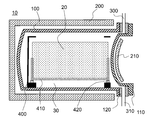
도 1은 본 발명의 제1 실시 형태에 따른 처리로의 측면 단면도이다.
도 2는 도 1의 지면 좌방향으로부터 본 처리로의 단면도이다.
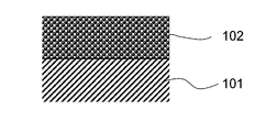
도 3은 본 발명의 제1 실시 형태에 따른 코팅막을 설명하는 도면이다.
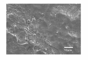
도 4는 본 발명의 코팅막 표면의 셀레늄화 처리 후의 SEM 사진이다.
도 5는 본 발명의 코팅막과 반응로의 기재의 선팽창 계수의 차이에 의한 효과를 설명하는 도면이다.
도 6은 본 발명의 제2 실시 형태에 따른 처리로의 측면 단면도이다.1 is a side sectional view of a processing furnace according to a first embodiment of the present invention.
FIG. 2 is a cross-sectional view of the processing furnace viewed from the leftward direction of the sheet in FIG. 1.
3 is a view for explaining a coating film according to the first embodiment of the present invention.
4 is a SEM photograph after selenization treatment of the coating film surface of the present invention.
5 is a view for explaining the effect of the difference in the coefficient of linear expansion of the substrate of the coating film and the reactor of the present invention.
6 is a side sectional view of a processing furnace according to a second embodiment of the present invention.
<제1 실시 형태><1st embodiment>
이하, 도면을 참조하면서 본 발명의 실시 형태를 설명한다. 도 1은 본 발명에 따른 셀레늄화 처리를 수행하는 기판 처리 장치에 구비되는 처리로(10)의 측면 단면도를 도시하고 있다. 또한, 도 2는 도 1의 지면 좌측으로부터 본 처리로의 단면도를 도시하고 있다.EMBODIMENT OF THE INVENTION Hereinafter, embodiment of this invention is described, referring drawings. 1 is a side cross-sectional view of a
처리로(10)는, 스테인리스 등의 금속 재료로 형성되는 노체로서의 반응관(100)을 포함한다. 반응관(100)은, 중공(中空)의 원통 형상을 하고 있으며, 그 일단(一端)이 폐색(閉塞)하고, 타단(他端)이 개구(開口)하는 구조를 가진다. 반응관(100)의 중공 부분에 의해, 처리실(30)이 형성된다. 반응관(100)의 개구측에는, 반응관(100)과 동심원 상에, 그 양단이 개구한 원통 형상의 매니폴드(120)가 설치된다. 반응관(100)과 매니폴드(120)와의 사이에는, 씰 부재로서의 O-링(도시하지 않음)이 설치되어 있다.The
매니폴드(120)의 반응관(100)이 설치되지 않은 개구부에는, 가동성(可動性)의 씰 캡(110)이 설치된다. 씰 캡(110)은, 스테인리스 등의 금속 재료로 형성되고, 매니폴드(120)의 개구부에 그 일부가 삽입되는 철(凸)형 형상을 하고 있다. 가동성의 씰 캡(110)과 매니폴드(120)와의 사이에는, 씰 부재로서의 O-링(도시하지 않음)이 설치되어, 처리를 수행할 때에는, 씰 캡(110)이 반응관(100)의 개구측을 기밀하게 폐색한다.A
반응관(100)의 내부에는, 구리(Cu), 인듐(In), 갈륨(Ga)을 함유하는 적층막이 형성된 복수의 유리 기판(예컨대, 30?40장)을 보지(保持)하는 카세트(410)를 재치(載置)하기 위한 이너월(inner wall, 400)이 설치된다. 이너월(400)은, 도 3에 도시되는 바와 같이, 그 일단이 반응관(100)의 내주면에 고정됨과 함께, 반응관(100)의 중심부에 카세트(410)가 설치대(420)를 개재하여 재치되도록 구성된다. 이너월(400)은, 카세트(410)를 사이에 두고 한 쌍의 부재가 그 양단에서 연결되도록 구성되어, 그 강도를 높게 하고 있다. 카세트(410)는, 도 1에 도시되는 바와 같이, 유리 기판(20)의 양단에, 복수의 유리 기판(20)을 세운 상태에서 횡방향으로 배열하여 보지 가능한 보지 부재를 포함한다. 또한, 양단의 보지 부재를 그 하면(下面)측에 설치된 한 쌍의 고정봉으로 고정하도록 하고, 복수의 유리 기판의 하단의 측면부는 반응실 내에 노출하도록 되어 있다. 또한, 카세트(410)의 양단을 고정하는 고정봉을, 양단의 보지 부재의 상단측에도 설치하여, 카세트(410)의 강도를 높여도 좋다.Inside the
또한, 반응관(100)을 둘러싸도록 일단이 폐색하고, 타단이 개구하는 중공의 원통 형상을 한 노체 가열부(200)가 설치된다. 또한, 씰 캡(110)의 반응관(100)과 반대측의 측면에는, 캡 가열부(210)가 설치된다. 이 노체 가열부(200)와 캡 가열부(210)에 의해 처리실(30) 내가 가열된다. 또한, 노체 가열부(200)는, 도시하지 않은 고정부에 의해 반응관(100)에 고정되고, 캡 가열부(210)는, 도시하지 않은 고정부에 의해 씰 캡(110)에 고정된다. 또한, 씰 캡(110)이나 매니폴드(120)에는, 내열성이 낮은 O-링을 보호하기 위해 도시하지 않은 수냉(水冷)의 냉각 수단이 설치된다.Moreover, the furnace heating
매니폴드(120)에는, 셀레늄 원소 함유 가스(셀레늄화원)로서의 수소화 셀레늄(이하, 「H2Se」)을 공급하기 위한 가스 공급관(300)이 설치된다. 가스 공급관(300)으로부터 공급된 H2Se는, 가스 공급관(300)으로부터 매니폴드(120)와 씰 캡(110)과의 사이의 간극(間隙)을 개재하여 처리실(30)로 공급된다. 또한, 가스 공급관(300)의 반대측의 매니폴드(120)에는, 배기관(310)이 설치된다. 처리실(30) 내의 분위기는, 매니폴드(120)와 씰 캡(110)과의 사이의 간극을 개재하여 배기관(310)으로부터 배기된다. 또한, 전술한 냉각 수단에 의해 냉각되는 개소(箇所)는, 150℃이하까지 냉각하면, 그 부분에 미반응의 셀레늄이 응축해버리기 때문에, 150℃~170℃정도로 온도 제어하면 좋다.The
여기서, 본 발명의 반응관(100)은, 스테인리스 등의 금속 재료로 형성되어 있다. 스테인리스 등의 금속 재료는, 석영과 비교하여 가공이 용이하다. 따라서, CIS계 태양 전지의 셀레늄화 처리를 수행하는 기판 처리 장치에 이용할 수 있을 것 같은 대형의 반응관(100)을 용이하게 제조하는 것이 가능해진다. 따라서, 반응관(100) 내에 수납할 수 있는 유리 기판의 수를 많게 할 수 있어, CIS계 태양 전지의 제조 비용을 내릴 수 있다.Here, the
또한, 본 실시 형태에서는, 반응관(100)의 적어도 처리실(30) 내의 분위기에 노출되는 표면은, 도 3에서 도시되는 바와 같이, 반응관(100)의 기재(101)가 되는 스테인리스 등의 금속 재료 상에, 스테인리스 등의 금속 재료와 비교하여 셀레늄화 내성이 높은 코팅막이 형성된다. 널리 이용되는 스테인리스 등의 금속 재료는, H2Se 등의 가스가 200℃이상으로 가열되면, 대단히 높은 반응성에 의해 부식되어버리지만, 본 실시 형태와 같이 셀레늄화 내성이 높은 코팅막을 형성하는 것에 의해, H2Se 등의 가스에 의한 부식을 억제할 수 있기 때문에, 널리 이용되는 스테인리스 등의 금속 재료를 이용할 수 있어, 기판 처리 장치의 제조 비용을 내리는 것이 가능해진다. 또한, 이 셀레늄화 내성이 높은 코팅막으로서는, 세라믹을 주성분으로 하는 코팅막, 예컨대, 산화크롬(CrxOy : x, y는 1이상의 임의의 수), 알루미나(AlxOy : x, y는 1이상의 임의의 수), 실리카(SixOy : x, y는 1이상의 임의의 수)의 각기 단독 혹은 혼합물, 또는, 탄소를 주성분으로 하는 코팅막, 예컨대, 탄화규소(SiC), DLC(diamond-like carbon)를 예로 들 수 있다.In addition, in this embodiment, the surface exposed to the atmosphere in the
또한, 본 실시 형태의 코팅막(102)은, 포러스 상(狀)의 막으로 형성하고 있다. 이에 의해, 반응관(100)의 스테인리스 등의 금속 재료로 형성되는 기재(101)와 코팅막(102)과의 선팽창 계수의 차이에 의한 열팽창?수축에 유연하게 추종하는 것이 가능해진다. 그 결과, 열처리를 반복하여 수행했다 하더라도, 코팅막으로의 균열의 발생을 최소한으로 억제할 수 있다. 또한, 코팅막은, 2?200μm, 바람직하게는 50?120μm의 두께로 형성하는 것이 바람직하다. 또한, 기재(101)와 코팅막(102)과의 선팽창 계수의 편차가 20%이하, 바람직하게는, 5%이하로 하는 것이 바람직하다.In addition, the
또한, 씰 캡(110), 매니폴드(120), 가스 공급관(300) 및 배기관(310)도 마찬가지로 셀레늄화원에 노출되는 부분에 전술한 코팅막을 형성해도 좋다. 단, O-링 등을 보호하기 위해 냉각 수단에 의해 200℃이하에 냉각되고 있는 부분은, 스테인리스 등의 금속 재료가 셀레늄화원과 접촉하여도 반응하지 않기 때문에 코팅하지 않아도 좋다.In addition, the
다음으로, 본 실시 형태의 처리로를 이용하여 수행하는, CIS계 태양 전지의 제조 방법의 일부인 기판의 제조 방법에 대하여 설명한다.Next, the manufacturing method of the board | substrate which is a part of the manufacturing method of a CIS system solar cell performed using the processing furnace of this embodiment is demonstrated.
우선, 구리(Cu), 인듐(In), 갈륨(Ga)을 함유하는 적층막이 형성된 30장~40장의 유리 기판을 카세트(410) 내에 준비하고, 가동성의 씰 캡(110)을 매니폴드(120)로부터 떼어낸 상태에서, 카세트(410)를 처리실(30) 내에 반입한다(반입 공정). 카세트의 반입은, 예컨대, 도시하지 않은 반입출(搬入出) 장치의 암에 의해 카세트 하부를 지지하여, 들어 올린 상태에서, 카세트(410)를 처리실(30) 내에 이동하여, 소정의 위치에 도달한 후, 해당 암을 하방으로 이동시켜 카세트(410)를 설치대(420)에 재치하는 것에 의해 수행된다.First, 30 to 40 glass substrates on which a laminated film containing copper (Cu), indium (In), and gallium (Ga) are formed are prepared in the
그 후, 처리실(30) 내를 질소 가스 등의 불활성 가스로 치환한다(치환 공정). 불활성 가스로 처리실(30) 내의 분위기를 치환한 후, 상온의 상태에서, 불활성 가스로 1?20%(바람직하게는, 2?10%)로 희석한 H2Se가스 등의 셀레늄화원을 가스 공급관(300)으로부터 도입한다. 다음으로, 상기 셀레늄화원을 봉입한 상태, 혹은, 배기관(310)으로부터 일정량(一定量) 배기하는 것에 의해 상기 셀레늄화원이 일정량 흐른 상태에서, 400?550℃, 바람직하게는 450℃?550℃까지, 매분 3?15℃로 승온(昇溫)한다. 소정 온도까지 승온한 후, 10?180분간, 바람직하게는, 20?120분간 보지하는 것에 의해, 셀레늄화 처리가 수행되어, CIS계 태양 전지의 광 흡수층이 형성된다(형성 공정).Thereafter, the
그 후, 가스 공급관(300)으로부터 불활성 가스를 도입하여, 처리실(30) 내의 분위기를 치환하고, 또, 소정 온도까지 강온(降溫)한다(강온 공정). 소정 온도까지 강온한 후, 씰 캡(110)을 이동시키는 것에 의해, 처리실(30)을 개구하고, 도시하지 않은 반입출 장치의 암으로 카세트(410)를 반출하는(반출 공정) 것에 의해 일련의 처리가 종료한다.Thereafter, an inert gas is introduced from the
스테인리스(SUS304)의 기재 상에, 본 발명의 코팅막을 형성하여, 가속 시험으로서 실제로 수행되는 셀레늄화 처리보다도 높은 650℃에서 셀레늄화 처리를 10회 수행한 후의 코팅막 표면의 SEM 사진을 도 4에 도시한다. 전술한 바와 같이 열처리를 반복한 것에 의해 수μm?수십μm의 미소 균열이 발생하고 있는 것을 알 수 있지만, 외관 상은 벗겨지는 듯한 징후는 전혀 없어 코팅막으로서 충분히 기능하고 있는 것을 알 수 있다.The SEM photograph of the surface of the coating film after forming the coating film of this invention on the base material of stainless steel (SUS304), and performing
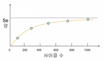
또한 코팅막의 셀레늄화 내성의 수명을 조사하기 위해, 셀레늄화 처리를 반복했을 때의 계면 및 코팅막 중에 축적 혹은 산화막으로부터 셀레늄화막으로 변화했을 때의 Se양을 평가하였다. 도 5는, 셀레늄화 처리 사이클 수와 계면 및 코팅막 중에 축적 혹은 산화막으로부터 셀레늄화막으로 변화했을 때의 Se양을 비교한 도면을 도시한다.In addition, in order to investigate the service life of selenization resistance of the coating film, the amount of Se when the selenization treatment was repeated and the amount of Se at the time of accumulation or change from the oxide film to the selenium film in the coating film was evaluated. FIG. 5 shows a comparison of the number of selenization treatment cycles and the amount of Se when accumulated or changed from an oxide film to a selenide film in an interface and a coating film.
상기 도 4에서 설명한 바와 같이, SUS304 상에 형성한 코팅막에서도 미소 균열은 발생하였어도 벗겨지는 징후는 전혀 볼 수 없었지만, 도 5에 있어서도 450℃에 있어서 1,000회까지 처리를 수행했지만 벗겨지는 징후는 전혀 보이지 않았다. 계면의 Se는 포화 경향을 나타내어 이 이상 셀레늄화 처리를 수행하여도 증가의 정도는 근소해질 것으로 추정된다. 연간의 가동율을 고려하면, 도 5의 A에서는 1,000회의 결과는, 양산에 있어서의 약 1년간 셀레늄화 처리를 수행한 경우의 결과에 상당한다. 여기에서는 1,000회까지밖에 검증할 수 없었지만, 이보다 처리 횟수를 늘려도 코팅의 상태에 변동이 보이지 않는 것으로부터, 원리적으로는 몇 배나 수명이 있다고 추정할 수 있다.As described with reference to FIG. 4, even when a micro crack was generated even in the coating film formed on SUS304, no signs of peeling were observed, but in FIG. 5, treatment was performed up to 1,000 times at 450 ° C., but no signs of peeling were observed. Did. The Se at the interface shows a saturation tendency, so that even if the selenization treatment is further performed, the degree of increase is estimated to be small. In consideration of the annual operation rate, the result of 1,000 times in A of FIG. 5 corresponds to the result when the selenization treatment is performed for about one year in mass production. In this case, only 1,000 times can be verified. However, even if the number of treatments is increased, it can be estimated that there is no change in the state of the coating.
<제2 실시 형태>≪ Second Embodiment >
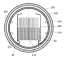
다음으로, 도 1 및 도 2에 도시되는 처리로(10)의 다른 실시 형태를 도 6을 이용하여 설명한다. 도 6에서는, 도 1 및 도 2와 동일한 기능을 가지는 부재에는 동일 번호를 달았다. 또한, 여기에서는, 제1 실시 형태와 상이한 점에 대하여 주로 설명한다.Next, another embodiment of the
도 6에 도시하는 제2 실시 형태에서는, 복수의 유리 기판(20)을 보지하는 카세트(410)를 하나만 재치한 제1 실시 형태와 다르게, 복수의 카세트(410)(여기에서는, 3개)를 복수의 유리 기판의 표면과 평행한 방향으로 배열하여 배치하고 있는 점이 다르다.In the second embodiment shown in FIG. 6, unlike the first embodiment in which only one
본 발명에서는, 종래의 석영제의 반응관을 이용하는 것이 아니라, 스테인리스 등의 금속 재료를 반응관(100)의 기재로서 이용하고 있다. 따라서, 반응관(100)을 대형화했다 하더라도, 석영제와 비교하여 그 성형이 용이하며, 또한, 그 비용의 증가도 석영제와 비교하여 작다. 그 때문에, 한 번에 처리할 수 있는 유리 기판(20)의 수를 많게 할 수 있어, CIS계 태양 전지의 제조 비용을 내릴 수 있다.In the present invention, instead of using a conventional quartz reaction tube, a metal material such as stainless steel is used as the base material of the
또한, 스테인리스 등의 금속 재료를 반응관의 기재로서 사용하는 것에 의해, 석영제의 반응관과 비교하여, 그 취급도 용이하며, 반응관을 대형화할 수 있다.Moreover, by using metal materials, such as stainless steel, as a base material of a reaction tube, compared with a quartz reaction tube, the handling is also easy and a reaction tube can be enlarged.
제1 실시 형태 및 제2 실시 형태에 있어서 본 발명에서는, 이하에 기재하는 효과 가운데 적어도 한 가지를 실현할 수 있다.In the present invention in the first and second embodiments, at least one of the effects described below can be realized.
(1) 반응관(100)의 기재(101)에 스테인리스 등의 금속 재료를 이용하는 것에 의해, 반응관(100)의 대형화가 용이해지며, 한 번에 처리할 수 있는 기판의 수를 많게 할 수 있다.(1) By using a metal material such as stainless steel as the
(2) 상기 (1)에 있어서, 반응관(100)의 기재(101) 상에, 셀레늄화 내성이 높은 코팅막(102)을 형성하는 것에 의해, 부식성이 높은 셀레늄원을 이용하는 처리를 수행할 수 있어, CIS계 태양 전지의 제조 비용을 내릴 수 있다.(2) In the above (1), by forming the
(3) 상기 (2)에 있어서, 코팅막(102)을 포러스 상으로 형성하는 것에 의해, 기재(101)와 코팅막(102)의 선팽창 계수의 차이에 기인하는 코팅막의 벗겨짐을 억제할 수 있다.(3) In the above (2), by forming the
(4) 상기 (2)에 있어서, 코팅막(102)과 기재(101)와의 선팽창 계수의 편차를 20%이하, 바람직하게는, 5%이하로 하는 것에 의해, 메인터넌스 주기를 크게 하는 것이 가능해진다.(4) In the above (2), the maintenance cycle can be increased by setting the variation in the coefficient of linear expansion between the
(5) 상기 (1)부터 (4) 중의 어느 하나에 있어서, 반응관(100) 내에는, 복수의 유리 기판(20)을 보지하는 카세트(410)를 유리 기판(20)의 표면과 평행한 방향으로 배열하여, 복수 개가 위치하는 것에 의해, 한 번에 처리할 수 있는 유리 기판의 수를 많게 할 수 있어, CIS계 태양 전지의 제조 비용을 작게 할 수 있다.(5) In any one of said (1)-(4), in the
이상, 본 발명의 실시 형태를 도면을 이용하여 설명하였지만, 본 발명의 취지를 일탈하지 않는 한, 여러 가지 변경이 가능하다. 예컨대, 전술한 실시 형태에서는, 구리(Cu), 인듐(In), 갈륨(Ga)이 형성된 복수의 유리 기판을 셀레늄화 처리하는 것으로 설명했지만, 이에 한하지 않고, 구리(Cu)/인듐(In)이나 구리(Cu)/갈륨(Ga) 등이 형성된 복수의 유리 기판을 셀레늄화 처리하도록 하여도 좋다. 또한, 본 실시 형태에서는, 금속 재료와의 반응성이 높은 셀레늄화에 대하여 언급했지만, CIS계 태양 전지에서는, 셀레늄화 처리를 대신하여 혹은 셀레늄화 처리 후에 유황 원소 함유 가스를 공급하여 유화 처리를 수행할 경우도 있다. 그 때도, 본 실시 형태의 대형 반응로를 이용하는 것에 의해, 한 번에 유화 처리를 할 수 있는 매수를 늘릴 수 있기 때문에, 제조 비용의 저하를 실현할 수 있다.As mentioned above, although embodiment of this invention was described using drawing, various changes are possible, unless deviating from the meaning of this invention. For example, in the above-mentioned embodiment, although the some glass substrate in which copper (Cu), indium (In), and gallium (Ga) were formed was described as selenium-processing, it is not limited to this, Copper (Cu) / indium (In) is mentioned. ), A plurality of glass substrates on which copper (Cu) / gallium (Ga) and the like are formed may be subjected to selenization. In addition, in the present embodiment, selenization having high reactivity with a metal material is mentioned, but in the CIS solar cell, an emulsification treatment may be performed by supplying a sulfur element-containing gas in place of or after selenization treatment. In some cases. In that case, since the number of sheets which can be emulsified at one time can be increased by using the large-scale reaction furnace of the present embodiment, a reduction in manufacturing cost can be realized.
마지막으로 본 발명의 바람직한 주요 형태를 이하에 부기한다.Finally, the preferable main form of this invention is appended below.
(1) 구리-인듐, 구리-갈륨 또는 구리-인듐-갈륨 중의 어느 하나로부터 이루어지는 적층막이 형성된 복수의 기판을 수납하는 처리실; 상기 처리실을 구성하도록 형성되는 반응관; 상기 처리실에 셀레늄 원소 함유 가스 또는 유황 원소 함유 가스를 도입하는 가스 공급관; 상기 처리실 내의 분위기를 배기하는 배기관; 및 상기 반응관을 둘러싸도록 설치된 가열부;를 구비하고, 상기 반응관의 기재는 금속 재료로 형성되는 기판 처리 장치.(1) a processing chamber for storing a plurality of substrates on which a laminated film made of any one of copper-indium, copper-gallium, or copper-indium-gallium is formed; A reaction tube formed to constitute the treatment chamber; A gas supply pipe for introducing a selenium element-containing gas or a sulfur element-containing gas into the processing chamber; An exhaust pipe exhausting the atmosphere in the processing chamber; And a heating unit provided to surround the reaction tube, wherein the substrate of the reaction tube is formed of a metal material.
(2) 상기 (1)에 있어서, 상기 반응관의 상기 처리실 측(側)의 표면 가운데 적어도 상기 셀레늄 원소 함유 가스 또는 상기 유황 원소 함유 가스에 노출되는 표면은, 상기 금속 재료보다도 상기 셀레늄 원소 함유 가스에 대한 부식 내성 또는 상기 유황 원소 함유 가스에 대한 부식 내성이 높은 재료에 의해 형성되는 코팅막을 포함하는 기판 처리 장치.(2) In the above-mentioned (1), the surface exposed to at least the selenium element-containing gas or the sulfur element-containing gas among the surfaces of the process chamber side of the reaction tube is the selenium element-containing gas than the metal material. And a coating film formed of a material having high corrosion resistance to or against the sulfur element-containing gas.
(3) 상기 (2)에 있어서, 상기 코팅막은, 세라믹스를 주성분으로 하는 코팅막 혹은 탄소를 주성분으로 하는 코팅막인 기판 처리 장치.(3) The substrate processing apparatus according to (2), wherein the coating film is a coating film containing ceramics as a main component or a coating film containing carbon as a main component.
(4) 상기 (2) 및 (3)중의 어느 하나에 있어서, 상기 코팅막은 포러스 상의 막인 기판 처리 장치.(4) The substrate processing apparatus according to any one of (2) and (3), wherein the coating film is a porous film.
(5) 상기 (2)부터 (4)중의 어느 하나에 있어서, 상기 코팅막은, 상기 반응관의 기재의 금속 재료와의 선팽창 계수의 편차가 20% 이하인 기판 처리 장치.(5) The substrate processing apparatus according to any one of (2) to (4), wherein the coating film has a variation in the coefficient of linear expansion with a metal material of the base of the reaction tube of 20% or less.
(6) 상기 (5)에 있어서, 상기 코팅막은, 상기 반응관의 기재의 금속 재료와의 선팽창 계수의 편차가 5% 이하인 기판 처리 장치.(6) The substrate processing apparatus according to (5), wherein the coating film has a variation in the coefficient of linear expansion with a metal material of the base of the reaction tube of 5% or less.
(7) 상기 (1)부터 (6)중의 어느 하나에 있어서, 상기 반응관의 기재의 금속 재료는, 스테인리스인 기판 처리 장치.(7) The substrate processing apparatus in any one of said (1)-(6) whose metal material of the base material of the said reaction tube is stainless steel.
(8) 상기 (1)부터 (7)중의 어느 하나에 있어서, 상기 카세트는, 상기 복수의 기판의 표면과 평행 방향으로 복수 배치되는 기판 처리 장치.(8) The substrate processing apparatus in any one of said (1)-(7) in which the said cassette is arranged in multiple numbers in parallel with the surfaces of the said several board | substrate.
(9) 구리-인듐, 구리-갈륨 또는 구리-인듐-갈륨 중의 어느 하나로부터 이루어지는 적층막이 형성된 복수의 기판을 금속 재료로 그 기재가 구성된 반응관의 내부에 구성되는 처리실에 수납하는 반입 공정; 상기 처리실을 가열하면서 상기 처리실에 셀레늄 원소 함유 가스 또는 유황 원소 함유 가스를 도입하여, 상기 복수의 기판을 셀레늄화 또는 유화하는 처리 공정; 및 상기 처리실 내의 상기 셀레늄 원소 함유 가스 또는 상기 유황 원소 함유 가스를 배기한 후, 상기 복수의 기판을 반출하는 반출 공정;을 포함하는 기판의 제조 방법 또는 CIS계 태양 전지의 제조 방법.(9) a carrying-in step of accommodating a plurality of substrates having a laminated film made of any one of copper-indium, copper-gallium, or copper-indium-gallium into a processing chamber configured inside a reaction tube composed of a metal material; A process step of introducing selenium element-containing gas or sulfur element-containing gas into the process chamber while heating the process chamber to selenize or emulsify the plurality of substrates; And a carrying-out step of carrying out the plurality of substrates after evacuating the selenium element-containing gas or the sulfur element-containing gas in the processing chamber.
10: 처리로 20: 유리 기판
30: 처리실 100: 반응관
101: 기재 102: 코팅막
110: 씰 캡 120: 매니폴드
200: 노체 가열부 210: 캡 가열부
300: 가스 공급관 310: 배기관
400: 이너월 410: 카세트
420: 설치대10: treatment furnace 20: glass substrate
30: process chamber 100: reaction tube
101: base material 102: coating film
110: seal cap 120: manifold
200: furnace heating portion 210: cap heating portion
300: gas supply pipe 310: exhaust pipe
400: inner wall 410: cassette
420: mounting table
Claims (10)
상기 처리실을 구성하도록 형성되는 반응관;
상기 처리실에 셀레늄 원소 함유 가스 또는 유황 원소 함유 가스를 도입하는 가스 공급관;
상기 처리실 내의 분위기를 배기하는 배기관; 및
상기 반응관을 둘러싸도록 설치된 가열부;
를 구비하고,
상기 반응관의 기재(基材)는 금속 재료로 형성되는 기판 처리 장치.A processing chamber accommodating a plurality of substrates on which a laminated film made of any one of copper-indium, copper-gallium, or copper-indium-gallium is formed;
A reaction tube formed to constitute the treatment chamber;
A gas supply pipe for introducing a selenium element-containing gas or a sulfur element-containing gas into the processing chamber;
An exhaust pipe exhausting the atmosphere in the processing chamber; And
A heating unit installed to surround the reaction tube;
And,
The base material of the said reaction tube is a substrate processing apparatus formed from a metal material.
상기 반응관의 상기 처리실 측(側)의 표면 가운데 적어도 상기 셀레늄 원소 함유 가스 또는 상기 유황 원소 함유 가스에 노출되는 표면은, 상기 금속 재료보다도 상기 셀레늄 원소 함유 가스에 대한 부식 내성 또는 상기 유황 원소 함유 가스에 대한 부식 내성이 높은 재료에 의해 형성되는 코팅막을 포함하는 기판 처리 장치.The method of claim 1,
The surface exposed to the selenium element-containing gas or the sulfur element-containing gas at least among the surfaces on the processing chamber side of the reaction tube is more resistant to corrosion to the selenium element-containing gas or the sulfur element-containing gas than the metal material. Substrate processing apparatus comprising a coating film formed by a material having high corrosion resistance to.
상기 코팅막은, 세라믹스를 주성분으로 하는 코팅막 혹은 탄소를 주성분으로 하는 코팅막인 기판 처리 장치.The method of claim 2,
The said coating film is a substrate processing apparatus which is a coating film which has ceramic as a main component, or the coating film which has carbon as a main component.
상기 코팅막은, 포러스 상(狀)의 막인 기판 처리 장치.The method of claim 2,
The said coating film is a substrate processing apparatus which is a porous film.
상기 코팅막은, 상기 반응관의 기재의 금속 재료와의 선팽창 계수의 편차가 20%이하인 기판 처리 장치.The method of claim 2,
The said coating film is a substrate processing apparatus whose deviation of the linear expansion coefficient with the metal material of the base material of the said reaction tube is 20% or less.
상기 코팅막은, 상기 반응관의 기재의 금속 재료와의 선팽창 계수의 편차가 5%이하인 기판 처리 장치.The method of claim 5,
The said coating film is a substrate processing apparatus whose deviation of the linear expansion coefficient with the metal material of the base material of the said reaction tube is 5% or less.
상기 반응관의 기재의 금속 재료는, 스테인리스인 기판 처리 장치.The method of claim 1,
The metal material of the base material of the said reaction tube is stainless steel.
상기 카세트는, 상기 복수의 기판의 표면과 평행 방향으로 복수 배치되는 기판 처리 장치.The method of claim 1,
And a plurality of cassettes are arranged in a direction parallel to the surfaces of the plurality of substrates.
상기 처리실을 가열하면서 상기 처리실에 셀레늄 원소 함유 가스 또는 유황 원소 함유 가스를 도입하여, 상기 복수의 기판을 셀레늄화 또는 유화(硫化)하는 처리 공정; 및
상기 처리실 내의 상기 셀레늄 원소 함유 가스 또는 상기 유황 원소 함유 가스를 배기한 후, 상기 복수의 기판을 반출하는 반출 공정;
을 포함하는 CIS계 태양 전지의 제조 방법.A carrying-in step of accommodating a plurality of substrates on which a laminated film made of any one of copper-indium, copper-gallium, or copper-indium-gallium is formed into a processing chamber configured inside a reaction tube composed of a metal material;
A processing step of introducing selenium element-containing gas or sulfur element-containing gas into the process chamber while heating the process chamber to selenize or emulsify the plurality of substrates; And
A carrying out step of carrying out the plurality of substrates after exhausting the selenium element-containing gas or the sulfur element-containing gas in the processing chamber;
Method for producing a CIS-based solar cell comprising a.
상기 처리실을 가열하면서 상기 처리실에 셀레늄 원소 함유 가스 또는 유황 원소 함유 가스를 도입하여, 상기 복수의 기판을 셀레늄화 또는 유화하는 처리 공정; 및
상기 처리실 내의 상기 셀레늄 원소 함유 가스 또는 상기 유황 원소 함유 가스를 배기한 후, 상기 복수의 기판을 반출하는 반출 공정;
을 포함하는 기판의 제조 방법.A carrying-in step of accommodating a plurality of substrates on which a laminated film made of any one of copper-indium, copper-gallium, or copper-indium-gallium is formed into a processing chamber configured inside a reaction tube composed of a metal material;
A process step of introducing selenium element-containing gas or sulfur element-containing gas into the process chamber while heating the process chamber to selenize or emulsify the plurality of substrates; And
A carrying out step of carrying out the plurality of substrates after exhausting the selenium element-containing gas or the sulfur element-containing gas in the processing chamber;
Method for producing a substrate comprising a.
Applications Claiming Priority (2)
| Application Number | Priority Date | Filing Date | Title |
|---|---|---|---|
| JP2011086642A JP2012222157A (en) | 2011-04-08 | 2011-04-08 | Substrate processing apparatus and method of manufacturing solar cell |
| JPJP-P-2011-086642 | 2011-04-08 |
Related Child Applications (1)
| Application Number | Title | Priority Date | Filing Date |
|---|---|---|---|
| KR20140158573A Division KR20150002556A (en) | 2011-04-08 | 2014-11-14 | Substrate processing apparatus, method for manufacturing solar battery and method for manufacturing substrate |
Publications (1)
| Publication Number | Publication Date |
|---|---|
| KR20120115091A true KR20120115091A (en) | 2012-10-17 |
Family
ID=46966423
Family Applications (2)
| Application Number | Title | Priority Date | Filing Date |
|---|---|---|---|
| KR1020120022171A KR20120115091A (en) | 2011-04-08 | 2012-03-05 | Substrate processing apparatus, method for manufacturing solar battery, and method for manufacturing substrate |
| KR20140158573A KR20150002556A (en) | 2011-04-08 | 2014-11-14 | Substrate processing apparatus, method for manufacturing solar battery and method for manufacturing substrate |
Family Applications After (1)
| Application Number | Title | Priority Date | Filing Date |
|---|---|---|---|
| KR20140158573A KR20150002556A (en) | 2011-04-08 | 2014-11-14 | Substrate processing apparatus, method for manufacturing solar battery and method for manufacturing substrate |
Country Status (5)
| Country | Link |
|---|---|
| US (1) | US20120258566A1 (en) |
| JP (1) | JP2012222157A (en) |
| KR (2) | KR20120115091A (en) |
| CN (1) | CN102738261B (en) |
| TW (1) | TWI462322B (en) |
Families Citing this family (5)
| Publication number | Priority date | Publication date | Assignee | Title |
|---|---|---|---|---|
| DE102015106693A1 (en) | 2015-04-29 | 2016-11-03 | Infineon Technologies Austria Ag | A superjunction semiconductor device with junction termination extension structure and method of fabrication |
| JP5741921B2 (en) * | 2011-04-08 | 2015-07-01 | 株式会社日立国際電気 | Substrate processing apparatus, method for forming coating film on surface of reaction tube used in substrate processing apparatus, and method for manufacturing solar cell |
| WO2014192871A1 (en) * | 2013-05-31 | 2014-12-04 | 株式会社日立国際電気 | Substrate processing apparatus, method for manufacturing semiconductor manufacturing apparatus, and furnace opening cover body |
| CN105531808A (en) * | 2013-09-10 | 2016-04-27 | 泰拉半导体株式会社 | Chamber for heat treatment device and method for manufacturing same |
| CN104677116B (en) * | 2014-12-30 | 2017-09-19 | 湖南顶立科技有限公司 | A kind of self-expansion type superhigh temperature heater |
Family Cites Families (11)
| Publication number | Priority date | Publication date | Assignee | Title |
|---|---|---|---|---|
| JP2855458B2 (en) * | 1989-12-15 | 1999-02-10 | 東芝セラミックス株式会社 | Processing material for semiconductor |
| US5273911A (en) * | 1991-03-07 | 1993-12-28 | Mitsubishi Denki Kabushiki Kaisha | Method of producing a thin-film solar cell |
| US5680013A (en) * | 1994-03-15 | 1997-10-21 | Applied Materials, Inc. | Ceramic protection for heated metal surfaces of plasma processing chamber exposed to chemically aggressive gaseous environment therein and method of protecting such heated metal surfaces |
| JP4380211B2 (en) * | 2002-08-30 | 2009-12-09 | 東ソー株式会社 | Quartz glass parts, manufacturing method thereof, and apparatus using the same |
| US20060240677A1 (en) * | 2002-09-20 | 2006-10-26 | Hitachi Kokusai Electric Inc., | Method for manufacturing semiconductor device and substrate processing apparatus |
| TW200832726A (en) * | 2006-11-10 | 2008-08-01 | Solopower Inc | Reel-to-reel reaction of precursor film to form solar cell absorber |
| US20080210168A1 (en) * | 2007-01-18 | 2008-09-04 | May Su | Single chamber, multiple tube high efficiency vertical furnace system |
| JP5154814B2 (en) * | 2007-03-29 | 2013-02-27 | 東ソー・クォーツ株式会社 | Method for producing quartz glass material |
| ES2581378T3 (en) * | 2008-06-20 | 2016-09-05 | Volker Probst | Processing device and procedure for processing stacked processing products |
| KR20110097908A (en) * | 2008-11-28 | 2011-08-31 | 볼커 프로브스트 | Method for producing semiconductor layers and coated substrates treated with elemental selenium and/or sulfur, in particular flat substrates |
| WO2011031521A2 (en) * | 2009-08-27 | 2011-03-17 | Applied Materials, Inc. | Method of decontamination of process chamber after in-situ chamber clean |
-
2011
- 2011-04-08 JP JP2011086642A patent/JP2012222157A/en active Pending
-
2012
- 2012-03-05 KR KR1020120022171A patent/KR20120115091A/en active Application Filing
- 2012-03-22 US US13/427,419 patent/US20120258566A1/en not_active Abandoned
- 2012-03-28 TW TW101110714A patent/TWI462322B/en active
- 2012-04-06 CN CN201210104813.6A patent/CN102738261B/en active Active
-
2014
- 2014-11-14 KR KR20140158573A patent/KR20150002556A/en not_active IP Right Cessation
Also Published As
| Publication number | Publication date |
|---|---|
| CN102738261A (en) | 2012-10-17 |
| TWI462322B (en) | 2014-11-21 |
| TW201251100A (en) | 2012-12-16 |
| JP2012222157A (en) | 2012-11-12 |
| KR20150002556A (en) | 2015-01-07 |
| US20120258566A1 (en) | 2012-10-11 |
| CN102738261B (en) | 2015-05-27 |
Similar Documents
| Publication | Publication Date | Title |
|---|---|---|
| KR101379748B1 (en) | Substrate processing apparatus, and transport device | |
| KR20120115091A (en) | Substrate processing apparatus, method for manufacturing solar battery, and method for manufacturing substrate | |
| EP2396450B1 (en) | A chemical vapour deposition system and process | |
| KR101500820B1 (en) | Arrangement, system, and method for processing multilayer bodies | |
| US9352431B2 (en) | Device for forming a reduced chamber space, and method for positioning multilayer bodies | |
| KR101366610B1 (en) | Substrate processing apparatus, and method for forming coating film on surface of reaction tube used for the substrate processing apparatus | |
| US20140060435A1 (en) | Doors for high volume, low cost system for epitaxial silicon deposition | |
| JP5069967B2 (en) | Manufacturing method of heat treatment member | |
| JP3203666U (en) | Window assembly for substrate processing system | |
| KR101543358B1 (en) | Method for improving property of graphite surface | |
| US20110203655A1 (en) | Photovoltaic device protection layer | |
| JP6316920B1 (en) | Equipment used for selenization and sulfidation of glass substrates | |
| CN113574683A (en) | Device, apparatus and method for the thermal treatment of a multilayer body of a thin-film solar module | |
| TW201338071A (en) | Substrate carrier and selenization process system thereof | |
| JP2008187067A (en) | Heat treatment equipment, heat insulation vacuum buffer, and heat insulation board | |
| WO2004005592A1 (en) | Thin sheet manufacturing apparatus and thin sheet manufacturing method | |
| TW201322472A (en) | Rapid thermal processing system and sulphidation method thereof | |
| WO2011135420A1 (en) | Process for the production of a compound semiconductor layer | |
| JP2009176861A (en) | Substrate processing apparatus, member for heat treatment and method of manufacturing member for heat treatment |
Legal Events
| Date | Code | Title | Description |
|---|---|---|---|
| A201 | Request for examination | ||
| E902 | Notification of reason for refusal | ||
| AMND | Amendment | ||
| E902 | Notification of reason for refusal | ||
| AMND | Amendment | ||
| E601 | Decision to refuse application | ||
| AMND | Amendment | ||
| A107 | Divisional application of patent | ||
| J201 | Request for trial against refusal decision | ||
| J301 | Trial decision |
Free format text: TRIAL DECISION FOR APPEAL AGAINST DECISION TO DECLINE REFUSAL REQUESTED 20141114 Effective date: 20160128 |