KR20120105469A - Apparatus and method for controllably implanting workpieces - Google Patents
Apparatus and method for controllably implanting workpieces Download PDFInfo
- Publication number
- KR20120105469A KR20120105469A KR1020127015077A KR20127015077A KR20120105469A KR 20120105469 A KR20120105469 A KR 20120105469A KR 1020127015077 A KR1020127015077 A KR 1020127015077A KR 20127015077 A KR20127015077 A KR 20127015077A KR 20120105469 A KR20120105469 A KR 20120105469A
- Authority
- KR
- South Korea
- Prior art keywords
- workpiece
- plasma
- ions
- focusing plate
- scanning
- Prior art date
Links
- 238000000034 method Methods 0.000 title claims description 52
- 150000002500 ions Chemical class 0.000 claims abstract description 97
- 238000002513 implantation Methods 0.000 claims abstract description 32
- 238000012545 processing Methods 0.000 claims abstract description 28
- 239000007943 implant Substances 0.000 claims abstract description 20
- 238000005468 ion implantation Methods 0.000 claims abstract description 9
- 238000002347 injection Methods 0.000 claims description 34
- 239000007924 injection Substances 0.000 claims description 34
- 239000002019 doping agent Substances 0.000 claims description 23
- 230000008569 process Effects 0.000 claims description 10
- 238000000605 extraction Methods 0.000 claims description 8
- 238000004886 process control Methods 0.000 claims description 6
- 230000001360 synchronised effect Effects 0.000 claims description 4
- 239000002184 metal Substances 0.000 claims 1
- 239000000758 substrate Substances 0.000 description 24
- 238000010586 diagram Methods 0.000 description 18
- 239000000463 material Substances 0.000 description 8
- 230000008021 deposition Effects 0.000 description 7
- 238000010884 ion-beam technique Methods 0.000 description 5
- 239000002245 particle Substances 0.000 description 5
- 230000001629 suppression Effects 0.000 description 5
- 230000007723 transport mechanism Effects 0.000 description 5
- 238000003491 array Methods 0.000 description 4
- 239000007789 gas Substances 0.000 description 4
- 238000012986 modification Methods 0.000 description 4
- 230000004048 modification Effects 0.000 description 4
- 239000004065 semiconductor Substances 0.000 description 4
- 238000004140 cleaning Methods 0.000 description 3
- 239000001257 hydrogen Substances 0.000 description 3
- 229910052739 hydrogen Inorganic materials 0.000 description 3
- 230000007246 mechanism Effects 0.000 description 3
- 230000000737 periodic effect Effects 0.000 description 3
- UFHFLCQGNIYNRP-UHFFFAOYSA-N Hydrogen Chemical compound [H][H] UFHFLCQGNIYNRP-UHFFFAOYSA-N 0.000 description 2
- 125000004429 atom Chemical group 0.000 description 2
- 230000008859 change Effects 0.000 description 2
- 239000004020 conductor Substances 0.000 description 2
- 230000000694 effects Effects 0.000 description 2
- 230000005684 electric field Effects 0.000 description 2
- 238000005530 etching Methods 0.000 description 2
- 230000004907 flux Effects 0.000 description 2
- 230000005484 gravity Effects 0.000 description 2
- 238000010438 heat treatment Methods 0.000 description 2
- 239000001307 helium Substances 0.000 description 2
- 229910052734 helium Inorganic materials 0.000 description 2
- SWQJXJOGLNCZEY-UHFFFAOYSA-N helium atom Chemical compound [He] SWQJXJOGLNCZEY-UHFFFAOYSA-N 0.000 description 2
- 239000012535 impurity Substances 0.000 description 2
- 238000001802 infusion Methods 0.000 description 2
- 239000012212 insulator Substances 0.000 description 2
- 238000001459 lithography Methods 0.000 description 2
- 238000004519 manufacturing process Methods 0.000 description 2
- 238000005259 measurement Methods 0.000 description 2
- 238000001208 nuclear magnetic resonance pulse sequence Methods 0.000 description 2
- OAICVXFJPJFONN-UHFFFAOYSA-N Phosphorus Chemical compound [P] OAICVXFJPJFONN-UHFFFAOYSA-N 0.000 description 1
- XUIMIQQOPSSXEZ-UHFFFAOYSA-N Silicon Chemical compound [Si] XUIMIQQOPSSXEZ-UHFFFAOYSA-N 0.000 description 1
- 238000005280 amorphization Methods 0.000 description 1
- -1 bit-patterned media Substances 0.000 description 1
- 230000005591 charge neutralization Effects 0.000 description 1
- 150000001875 compounds Chemical class 0.000 description 1
- 238000001816 cooling Methods 0.000 description 1
- 238000012937 correction Methods 0.000 description 1
- 239000013078 crystal Substances 0.000 description 1
- 230000007423 decrease Effects 0.000 description 1
- 238000013461 design Methods 0.000 description 1
- 238000009826 distribution Methods 0.000 description 1
- 238000005516 engineering process Methods 0.000 description 1
- 230000007613 environmental effect Effects 0.000 description 1
- 239000011521 glass Substances 0.000 description 1
- 150000002431 hydrogen Chemical class 0.000 description 1
- 230000006872 improvement Effects 0.000 description 1
- 238000011065 in-situ storage Methods 0.000 description 1
- 238000009616 inductively coupled plasma Methods 0.000 description 1
- 238000004020 luminiscence type Methods 0.000 description 1
- 238000012423 maintenance Methods 0.000 description 1
- 239000011159 matrix material Substances 0.000 description 1
- 230000007935 neutral effect Effects 0.000 description 1
- 229910052756 noble gas Inorganic materials 0.000 description 1
- 150000002835 noble gases Chemical class 0.000 description 1
- 229910052698 phosphorus Inorganic materials 0.000 description 1
- 239000011574 phosphorus Substances 0.000 description 1
- 230000003449 preventive effect Effects 0.000 description 1
- 238000005086 pumping Methods 0.000 description 1
- 229910052710 silicon Inorganic materials 0.000 description 1
- 239000010703 silicon Substances 0.000 description 1
- 239000007787 solid Substances 0.000 description 1
- 238000010561 standard procedure Methods 0.000 description 1
- 239000010409 thin film Substances 0.000 description 1
- 235000012431 wafers Nutrition 0.000 description 1
Images


Classifications
-
- H—ELECTRICITY
- H01—ELECTRIC ELEMENTS
- H01J—ELECTRIC DISCHARGE TUBES OR DISCHARGE LAMPS
- H01J37/00—Discharge tubes with provision for introducing objects or material to be exposed to the discharge, e.g. for the purpose of examination or processing thereof
- H01J37/30—Electron-beam or ion-beam tubes for localised treatment of objects
- H01J37/317—Electron-beam or ion-beam tubes for localised treatment of objects for changing properties of the objects or for applying thin layers thereon, e.g. for ion implantation
-
- B—PERFORMING OPERATIONS; TRANSPORTING
- B01—PHYSICAL OR CHEMICAL PROCESSES OR APPARATUS IN GENERAL
- B01J—CHEMICAL OR PHYSICAL PROCESSES, e.g. CATALYSIS OR COLLOID CHEMISTRY; THEIR RELEVANT APPARATUS
- B01J19/00—Chemical, physical or physico-chemical processes in general; Their relevant apparatus
- B01J19/08—Processes employing the direct application of electric or wave energy, or particle radiation; Apparatus therefor
- B01J19/081—Processes employing the direct application of electric or wave energy, or particle radiation; Apparatus therefor employing particle radiation or gamma-radiation
-
- H—ELECTRICITY
- H01—ELECTRIC ELEMENTS
- H01J—ELECTRIC DISCHARGE TUBES OR DISCHARGE LAMPS
- H01J37/00—Discharge tubes with provision for introducing objects or material to be exposed to the discharge, e.g. for the purpose of examination or processing thereof
- H01J37/30—Electron-beam or ion-beam tubes for localised treatment of objects
- H01J37/317—Electron-beam or ion-beam tubes for localised treatment of objects for changing properties of the objects or for applying thin layers thereon, e.g. for ion implantation
- H01J37/3171—Electron-beam or ion-beam tubes for localised treatment of objects for changing properties of the objects or for applying thin layers thereon, e.g. for ion implantation for ion implantation
-
- H—ELECTRICITY
- H01—ELECTRIC ELEMENTS
- H01J—ELECTRIC DISCHARGE TUBES OR DISCHARGE LAMPS
- H01J37/00—Discharge tubes with provision for introducing objects or material to be exposed to the discharge, e.g. for the purpose of examination or processing thereof
- H01J37/32—Gas-filled discharge tubes
- H01J37/32009—Arrangements for generation of plasma specially adapted for examination or treatment of objects, e.g. plasma sources
- H01J37/32357—Generation remote from the workpiece, e.g. down-stream
-
- H—ELECTRICITY
- H01—ELECTRIC ELEMENTS
- H01J—ELECTRIC DISCHARGE TUBES OR DISCHARGE LAMPS
- H01J37/00—Discharge tubes with provision for introducing objects or material to be exposed to the discharge, e.g. for the purpose of examination or processing thereof
- H01J37/32—Gas-filled discharge tubes
- H01J37/32009—Arrangements for generation of plasma specially adapted for examination or treatment of objects, e.g. plasma sources
- H01J37/32422—Arrangement for selecting ions or species in the plasma
-
- H—ELECTRICITY
- H01—ELECTRIC ELEMENTS
- H01J—ELECTRIC DISCHARGE TUBES OR DISCHARGE LAMPS
- H01J37/00—Discharge tubes with provision for introducing objects or material to be exposed to the discharge, e.g. for the purpose of examination or processing thereof
- H01J37/32—Gas-filled discharge tubes
- H01J37/32431—Constructional details of the reactor
- H01J37/32623—Mechanical discharge control means
-
- H—ELECTRICITY
- H01—ELECTRIC ELEMENTS
- H01L—SEMICONDUCTOR DEVICES NOT COVERED BY CLASS H10
- H01L21/00—Processes or apparatus adapted for the manufacture or treatment of semiconductor or solid state devices or of parts thereof
- H01L21/02—Manufacture or treatment of semiconductor devices or of parts thereof
- H01L21/04—Manufacture or treatment of semiconductor devices or of parts thereof the devices having at least one potential-jump barrier or surface barrier, e.g. PN junction, depletion layer or carrier concentration layer
- H01L21/18—Manufacture or treatment of semiconductor devices or of parts thereof the devices having at least one potential-jump barrier or surface barrier, e.g. PN junction, depletion layer or carrier concentration layer the devices having semiconductor bodies comprising elements of Group IV of the Periodic System or AIIIBV compounds with or without impurities, e.g. doping materials
- H01L21/26—Bombardment with radiation
- H01L21/263—Bombardment with radiation with high-energy radiation
- H01L21/265—Bombardment with radiation with high-energy radiation producing ion implantation
-
- H—ELECTRICITY
- H01—ELECTRIC ELEMENTS
- H01L—SEMICONDUCTOR DEVICES NOT COVERED BY CLASS H10
- H01L31/00—Semiconductor devices sensitive to infrared radiation, light, electromagnetic radiation of shorter wavelength or corpuscular radiation and specially adapted either for the conversion of the energy of such radiation into electrical energy or for the control of electrical energy by such radiation; Processes or apparatus specially adapted for the manufacture or treatment thereof or of parts thereof; Details thereof
- H01L31/02—Details
- H01L31/0224—Electrodes
- H01L31/022408—Electrodes for devices characterised by at least one potential jump barrier or surface barrier
- H01L31/022425—Electrodes for devices characterised by at least one potential jump barrier or surface barrier for solar cells
-
- H—ELECTRICITY
- H01—ELECTRIC ELEMENTS
- H01L—SEMICONDUCTOR DEVICES NOT COVERED BY CLASS H10
- H01L31/00—Semiconductor devices sensitive to infrared radiation, light, electromagnetic radiation of shorter wavelength or corpuscular radiation and specially adapted either for the conversion of the energy of such radiation into electrical energy or for the control of electrical energy by such radiation; Processes or apparatus specially adapted for the manufacture or treatment thereof or of parts thereof; Details thereof
- H01L31/04—Semiconductor devices sensitive to infrared radiation, light, electromagnetic radiation of shorter wavelength or corpuscular radiation and specially adapted either for the conversion of the energy of such radiation into electrical energy or for the control of electrical energy by such radiation; Processes or apparatus specially adapted for the manufacture or treatment thereof or of parts thereof; Details thereof adapted as photovoltaic [PV] conversion devices
- H01L31/06—Semiconductor devices sensitive to infrared radiation, light, electromagnetic radiation of shorter wavelength or corpuscular radiation and specially adapted either for the conversion of the energy of such radiation into electrical energy or for the control of electrical energy by such radiation; Processes or apparatus specially adapted for the manufacture or treatment thereof or of parts thereof; Details thereof adapted as photovoltaic [PV] conversion devices characterised by at least one potential-jump barrier or surface barrier
- H01L31/068—Semiconductor devices sensitive to infrared radiation, light, electromagnetic radiation of shorter wavelength or corpuscular radiation and specially adapted either for the conversion of the energy of such radiation into electrical energy or for the control of electrical energy by such radiation; Processes or apparatus specially adapted for the manufacture or treatment thereof or of parts thereof; Details thereof adapted as photovoltaic [PV] conversion devices characterised by at least one potential-jump barrier or surface barrier the potential barriers being only of the PN homojunction type, e.g. bulk silicon PN homojunction solar cells or thin film polycrystalline silicon PN homojunction solar cells
-
- H—ELECTRICITY
- H01—ELECTRIC ELEMENTS
- H01L—SEMICONDUCTOR DEVICES NOT COVERED BY CLASS H10
- H01L31/00—Semiconductor devices sensitive to infrared radiation, light, electromagnetic radiation of shorter wavelength or corpuscular radiation and specially adapted either for the conversion of the energy of such radiation into electrical energy or for the control of electrical energy by such radiation; Processes or apparatus specially adapted for the manufacture or treatment thereof or of parts thereof; Details thereof
- H01L31/08—Semiconductor devices sensitive to infrared radiation, light, electromagnetic radiation of shorter wavelength or corpuscular radiation and specially adapted either for the conversion of the energy of such radiation into electrical energy or for the control of electrical energy by such radiation; Processes or apparatus specially adapted for the manufacture or treatment thereof or of parts thereof; Details thereof in which radiation controls flow of current through the device, e.g. photoresistors
-
- H—ELECTRICITY
- H01—ELECTRIC ELEMENTS
- H01L—SEMICONDUCTOR DEVICES NOT COVERED BY CLASS H10
- H01L31/00—Semiconductor devices sensitive to infrared radiation, light, electromagnetic radiation of shorter wavelength or corpuscular radiation and specially adapted either for the conversion of the energy of such radiation into electrical energy or for the control of electrical energy by such radiation; Processes or apparatus specially adapted for the manufacture or treatment thereof or of parts thereof; Details thereof
- H01L31/18—Processes or apparatus specially adapted for the manufacture or treatment of these devices or of parts thereof
- H01L31/1804—Processes or apparatus specially adapted for the manufacture or treatment of these devices or of parts thereof comprising only elements of Group IV of the Periodic System
-
- H—ELECTRICITY
- H01—ELECTRIC ELEMENTS
- H01J—ELECTRIC DISCHARGE TUBES OR DISCHARGE LAMPS
- H01J2237/00—Discharge tubes exposing object to beam, e.g. for analysis treatment, etching, imaging
- H01J2237/04—Means for controlling the discharge
- H01J2237/045—Diaphragms
- H01J2237/0451—Diaphragms with fixed aperture
- H01J2237/0453—Diaphragms with fixed aperture multiple apertures
-
- H—ELECTRICITY
- H01—ELECTRIC ELEMENTS
- H01J—ELECTRIC DISCHARGE TUBES OR DISCHARGE LAMPS
- H01J2237/00—Discharge tubes exposing object to beam, e.g. for analysis treatment, etching, imaging
- H01J2237/10—Lenses
- H01J2237/12—Lenses electrostatic
- H01J2237/1205—Microlenses
-
- H—ELECTRICITY
- H01—ELECTRIC ELEMENTS
- H01L—SEMICONDUCTOR DEVICES NOT COVERED BY CLASS H10
- H01L21/00—Processes or apparatus adapted for the manufacture or treatment of semiconductor or solid state devices or of parts thereof
- H01L21/02—Manufacture or treatment of semiconductor devices or of parts thereof
- H01L21/04—Manufacture or treatment of semiconductor devices or of parts thereof the devices having at least one potential-jump barrier or surface barrier, e.g. PN junction, depletion layer or carrier concentration layer
- H01L21/18—Manufacture or treatment of semiconductor devices or of parts thereof the devices having at least one potential-jump barrier or surface barrier, e.g. PN junction, depletion layer or carrier concentration layer the devices having semiconductor bodies comprising elements of Group IV of the Periodic System or AIIIBV compounds with or without impurities, e.g. doping materials
- H01L21/22—Diffusion of impurity materials, e.g. doping materials, electrode materials, into or out of a semiconductor body, or between semiconductor regions; Interactions between two or more impurities; Redistribution of impurities
- H01L21/223—Diffusion of impurity materials, e.g. doping materials, electrode materials, into or out of a semiconductor body, or between semiconductor regions; Interactions between two or more impurities; Redistribution of impurities using diffusion into or out of a solid from or into a gaseous phase
- H01L21/2236—Diffusion of impurity materials, e.g. doping materials, electrode materials, into or out of a semiconductor body, or between semiconductor regions; Interactions between two or more impurities; Redistribution of impurities using diffusion into or out of a solid from or into a gaseous phase from or into a plasma phase
-
- Y—GENERAL TAGGING OF NEW TECHNOLOGICAL DEVELOPMENTS; GENERAL TAGGING OF CROSS-SECTIONAL TECHNOLOGIES SPANNING OVER SEVERAL SECTIONS OF THE IPC; TECHNICAL SUBJECTS COVERED BY FORMER USPC CROSS-REFERENCE ART COLLECTIONS [XRACs] AND DIGESTS
- Y02—TECHNOLOGIES OR APPLICATIONS FOR MITIGATION OR ADAPTATION AGAINST CLIMATE CHANGE
- Y02E—REDUCTION OF GREENHOUSE GAS [GHG] EMISSIONS, RELATED TO ENERGY GENERATION, TRANSMISSION OR DISTRIBUTION
- Y02E10/00—Energy generation through renewable energy sources
- Y02E10/50—Photovoltaic [PV] energy
- Y02E10/547—Monocrystalline silicon PV cells
-
- Y—GENERAL TAGGING OF NEW TECHNOLOGICAL DEVELOPMENTS; GENERAL TAGGING OF CROSS-SECTIONAL TECHNOLOGIES SPANNING OVER SEVERAL SECTIONS OF THE IPC; TECHNICAL SUBJECTS COVERED BY FORMER USPC CROSS-REFERENCE ART COLLECTIONS [XRACs] AND DIGESTS
- Y02—TECHNOLOGIES OR APPLICATIONS FOR MITIGATION OR ADAPTATION AGAINST CLIMATE CHANGE
- Y02P—CLIMATE CHANGE MITIGATION TECHNOLOGIES IN THE PRODUCTION OR PROCESSING OF GOODS
- Y02P70/00—Climate change mitigation technologies in the production process for final industrial or consumer products
- Y02P70/50—Manufacturing or production processes characterised by the final manufactured product
Abstract
플라즈마 공정 장치(processing apparatus)는 플라즈마 챔버에 플라즈마를 생산하기 위해 구성된 플라즈마 소스를 포함하여, 플라즈마는 워크피스에 주입을 위한 이온들을 수용한다. 장치들은 집속 플레이트(focusing plate) 근처의 플라즈마 시스(plasma sheath)의 모양(shape)을 변형하도록 구성된 개구 배열(arrangement)를 가지는 집속 플레이트를 또한 포함하여 이온들이 집속된 이온들을 정의하기 위해 개구 배열을 빠져나간다. 장치들은 집속 플레이트로부터 분리된 워크피스를 수용하는 공정 챔버(processing chamber)를 추가로 포함하여 워크피스에 집속된 이온들의 정지 주입 영역이 개구보다 실질적으로 더 좁다. 장치들은 이온 주입 동안에 워크피스를 주사(scanning)함으로써 워크피스에 복수개의 패턴화된 영역들을 생성하도록 구성된다. The plasma processing apparatus includes a plasma source configured to produce a plasma in a plasma chamber, where the plasma receives ions for implantation into the workpiece. The devices also include a focusing plate having an array arrangement configured to modify the shape of the plasma sheath near the focusing plate to define the apertured arrangement to define the ions to which the ions are focused. Exit The devices further include a processing chamber that receives the workpiece separated from the focusing plate so that the stationary implant region of ions focused on the workpiece is substantially narrower than the opening. The devices are configured to create a plurality of patterned regions in the workpiece by scanning the workpiece during ion implantation.
Description
본 발명은 워크피스(workpiece)들의 주입(implantation)에 관한 것으로, 보다 상세하게는 워크피스들의 집속된(focused) 주입을 위한 방법 및 장치에 관한 것이다.The present invention relates to implantation of workpieces, and more particularly, to a method and apparatus for focused implantation of workpieces.
이온 주입(ion implantation)은 기판들에 성질-전환(property-altering) 불순물들을 도입하기 위한 표준 기술이다. 소정의(desired) 불순물(impurity) 물질이 이온 소스(ion source)로 이온화되고, 이온들이 미리 정해진(prescribed) 에너지의 이온 빔을 형성하기 위해 가속되고, 그리고 이온 빔은 기판의 표면에 향하게 된다. 빔에 활동적인 이온들은 기판 물질의 서브-표면(sub-surface)를 투과하고 소정의 전도성 영역 또는 물질 성질(material property) 영역을 형성하기 위해 기판 물질의 결정질 격자(crystalline lattice)에 내장된다.Ion implantation is a standard technique for introducing property-altering impurities into substrates. Desired impurity material is ionized to an ion source, ions are accelerated to form an ion beam of predetermined energy, and the ion beam is directed to the surface of the substrate. Ions active in the beam are embedded in the crystalline lattice of the substrate material to penetrate the sub-surface of the substrate material and form a desired conductive or material property region.
솔라 셀들은 비용없이 자연 자원을 이용하는 무공해(pollution-free), 동등한-접근(equal-access) 에너지를 제공한다. 환경의 관심과 에너지 경비의 증가 때문에, 실리콘 기판들로 구성될 수 있는 솔라 셀들은 더 세계적으로 중요해지고 있다. 고성능(high-performance) 솔라 셀들의 생산 또는 제조를 위한 어떤 절감된 경비 또는 고성능 솔라 셀들에 어떤 효율 개선은 전세계적인 솔라 셀들의 완성(implementation)에 긍정적인 영향이 된다. 이것은 이 청정 에너지 기술의 폭넓은 유용성이 가능하게 할 것이다. Solar cells provide polllution-free, equal-access energy using natural resources at no cost. Due to environmental concerns and increased energy costs, solar cells that can be made of silicon substrates are becoming more important worldwide. Any reduced cost for the production or manufacture of high-performance solar cells or any efficiency improvement in high-performance solar cells has a positive impact on the implementation of solar cells worldwide. This will enable wider utility of this clean energy technology.
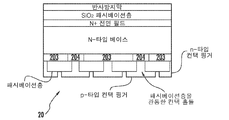
도핑은 솔라 셀들의 효율(efficiency)을 개선할 수 있다. 이 도핑은 이온 주입(ion implantation)을 이용하여 수행될 수 있다. 도 1 은 선택적 에미터 솔라 셀(selective emitter solar cell)(10)의 단면도(cross-sectional view)이다. 에미터(200)을 도핑하고 컨택들(202) 아래 영역들(201)에 추가적인 도펀트(dopant)를 제공하는 것은 솔라 셀의 효율(전기적 에너지로 변환된 광(light)의 퍼센트)을 증가시킬 수 있다. 영역들(201)을 고농도(heavily) 도핑하는 것은 전도성(conductivity)을 개선시키고 컨택들(202)사이에 저농도(less) 도핑을 하는 것은 전하 수집(charge collection)을 개선한다. 컨택들(202)은 약 2-3mm 떨어져 분리될 수 있다. 영역들(201)은 약 100-300㎛ 걸쳐서 단지 존재할 수 있다. 도 2 는 서로 얽힌 후면 접촉(IBC : interdigitated back contact) 솔라 셀(20)의 단면도(cross-sectional view)이다. IBC 솔라 셀(20)에서, 접합은 솔라 셀의 후면 상에 있다. 특정 실시예에서 도핑 패턴은 p-타입과 n-타입 도펀트 영역들이 교호(alternating)하고 있다. p+ 에미터(203) 와 n+ 후표면 필드(back surface field)(204)는 도핑될 수 있다. 이 도핑은 IBC 솔라 셀에 접합이 제대로 기능하거나(function) 또는 증가된 효율을 가질 수 있도록 할 수 있다. Doping may improve the efficiency of the solar cells. This doping can be performed using ion implantation. 1 is a cross-sectional view of a selective emitter
하이 도즈(high dose) 주입이 주입기(implanter)를 위한 최소 소유 비용(cost-of-ownership)을 허용할 수 있다. 국부화된(localized) 또는 선택적인 도핑 또는 국부화된 또는 선택적인 물질 변형(material modification)은 어떤 주입을 필요로 할 수 있다. 주입과 함께 리소그라피(lithography)의 이용은 추가 단계들을 필요로 하기 때문에 선택적인 주입들을 위해 엄두를 못 낼 정도로 너무 비용이 높을 수 있다. 플라즈마 도핑 기술은 이런 응용(application)들을 위해서 충분히 테스트되지 않았다. 플라즈마에서 중립자(neutral)들에 직접 노출(exposure)은 워크피스의 증착(deposition) 또는 에칭(etching)을 야기할 수 있고, 추가적인 세정(cleaning) 단계들을 필요로 할 수 있다. 따라서, 워크피스들의 개선된 주입을 위한 기술 요구가 있고 그리고 보다 상세하게는, 워크피스들의 집속된(focused) 주입을 위한 개선된 방법 및 장치에 관한 것이다.High dose injection may allow a cost-of-ownership for the implanter. Localized or selective doping or localized or selective material modification may require some injection. The use of lithography with infusions can be too costly for the selective infusions since the use of lithography requires additional steps. Plasma doping techniques have not been fully tested for these applications. Direct exposure to neutrals in the plasma may cause deposition or etching of the workpiece and may require additional cleaning steps. Accordingly, there is a technical need for improved implantation of workpieces and more particularly, to an improved method and apparatus for focused implantation of workpieces.
일 실시예에서, 공정 장치(processing apparatus)들은 워크피스에 주입을 위한 이온들을 수용하는 플라즈마가 있는 플라즈마 챔버에서 플라즈마를 생산하기 위해 구성된 플라즈마 소스를 포함한다. 장치들은 집속 플레이트(focusing plate) 근처의 플라즈마 시스(plasma sheath)의 모양(shape)을 변형하도록 구성된 개구를 가지는 집속 플레이트를 또한 포함하여 집속된 이온들을 정의하기 위해 이온들이 개구를 빠져나간다. 장치들은 집속된 이온들이 개구보다 실질적으로 좁은 주입 폭(width)을 가지며, 집속 플레이트로부터 분리된 워크피스를 수용하는 공정 챔버(processing chamber)를 추가로 포함한다. 장치들은 이온 주입 동안에 워크피스를 주사(scanning)함으로써 복수개(a plurality of)의 패턴화된 영역들을 생성하도록 구성된다. In one embodiment, the processing apparatus includes a plasma source configured to produce a plasma in a plasma chamber having a plasma that receives ions for implantation in a workpiece. The devices also include a focusing plate having an opening configured to modify the shape of the plasma sheath near the focusing plate so that the ions exit the opening to define focused ions. The apparatus further includes a processing chamber in which the focused ions have an implant width substantially narrower than the opening and receive a workpiece separated from the focusing plate. The devices are configured to generate a plurality of patterned regions by scanning the workpiece during ion implantation.
다른 실시예에서, 플라즈마 공정 시스템에서 워크피스에 주입 방법은 플라즈마를 수용하는 플라즈마 챔버 근처에 집속 플레이트를 제공하는 단계를 포함하고,상기 집속 플레이트(focusing plate)는 워크피스에 대하여 집속된 이온들을 제공하는 적어도 하나의 개구를 관통하여 플라즈마로부터 이온들을 추출하도록 구성된 개구 배열(arrangement)을 가진다. 방법은 워크피스에 집속된 이온들을 끌어당기기 위해서 워크피스 홀더와 플라즈마 사이에 바이어스(bias)를 제공하는 단계, 복수개의 선택적으로 주입된 영역들을 생산하기 위해서 집속 플레이트에 대하여 워크피스 홀더를 주사하는 단계를 추가로 포함한다.In another embodiment, a method of implanting into a workpiece in a plasma processing system includes providing a focusing plate near a plasma chamber containing a plasma, wherein the focusing plate provides focused ions for the workpiece. Has an aperture arrangement configured to extract ions from the plasma through at least one aperture. The method includes providing a bias between the workpiece holder and the plasma to attract ions focused on the workpiece, and scanning the workpiece holder against the focusing plate to produce a plurality of selectively implanted regions. It further includes.
본 발명은 더 나은 이해를 위해서 첨부하는 도면들에 참조번호(reference)가 제공되고, 도면들은 참조로서 명세서에 부가된다.
도 1 은 주지의 선택적 에미터(selective emitter) 솔라 셀의 단면도이다.
도 2 는 주지의 서로 얽힌 후면 접촉(interdigitated back contact) 솔라 셀의 단면도(cross-sectional view)이다.
도 3 은 플라즈마 시스템 내에 집속 플레이트 배열의 단면도이다.
도 4 는 주입된 솔라 셀 실시예의 평면도(top view)이다.
도 5 는 본 발명의 제 1 실시예에 일치하는 플라즈마 공정 장치들의 블럭도이다.
도 6 은 본 발명의 제 2 실시예에 일치하는 플라즈마 공정 장치들의 블럭도이다.
도 7 은 본 발명의 제 3 실시예에 일치하는 플라즈마 공정 장치들의 블럭도이다.
도 8 은 본 발명의 제 4 실시예에 일치하는 플라즈마 공정 장치들의 블럭도이다.
도 9 는 본 발명의 제 5 실시예에 일치하는 플라즈마 공정 장치들의 블럭도이다.
도 10 은 본 발명의 제 6 실시예에 일치하는 플라즈마 공정 장치들의 블럭도이다.
도 11 은 본 발명의 제 7 실시예에 일치하는 플라즈마 공정 장치들의 블럭도이다.
도 12 는 본 발명의 제 8 실시예에 일치하는 플라즈마 공정 장치들의 블럭도이다.
도 13 은 집속 플레이트(focusing plate)의 일 실시예의 단면도이다.
도 14 는 주입 동안에 스텝화된(stepped) 이동(movement)을 예시하는 단면도이다.
도 15a-15d 는 이온 도즈와 주사 속도(scanning velocity)간의 관계를 예시한다.
도 16 는 정전기 억제(electrostatic suppression)의 일 실시예를 예시하는 단면도이다.
도 17a-b 는 자기 억제(magnetic suppression)의 두개 실시예를 예시하는 단면도이다.
도 18 - 19 는 워크피스를 두개 도펀트 수준(level)으로 주입하기 위해 RF 또는 DC 동기화(synchronization)를 채용하는 발명의 실시예들에 관여된 대표적인 단계들을 예시한다.
도 20a 및 20b 는 각각 워크피스의 단면도 그리고 주입 전 및 주입 후 집속 플레이트 시스템의 단면도이다.
도 20c 는 주입된 영역들을 나타내는 주입 후에 도 20a-b의 워크피스의 도식적인 평면도이다.
도 20d 는 주입 동안에 워크피스 및 집속 플레이트 시스템의 평면도이다.
도 20e 는 주입된 영역들을 나타내는 도 20d의 워크피스의 도식적인 평면도이다.
도 21 는 공정 제어 장치의 정면도(front view)이다.
도 22 는 본 발명의 제 9 실시예에 일치하는 플라즈마 공정 장치들의 블럭도이다.
도 23-24 는 펄스화된(pulsed) 주입 실시예들에 따라 대표적인 전압 및 워크피스 위치를 시간의 함수로서 예시한다.BRIEF DESCRIPTION OF THE DRAWINGS The present invention is provided with reference to the accompanying drawings for a better understanding, which is added to the specification by reference.
1 is a cross-sectional view of a known selective emitter solar cell.
2 is a cross-sectional view of a well known interdigitated back contact solar cell.
3 is a cross-sectional view of a focusing plate arrangement in a plasma system.
4 is a top view of an implanted solar cell embodiment.
5 is a block diagram of a plasma processing apparatus in accordance with a first embodiment of the present invention.
6 is a block diagram of plasma processing apparatuses in accordance with a second embodiment of the present invention.
7 is a block diagram of plasma processing apparatuses in accordance with a third embodiment of the present invention.
8 is a block diagram of plasma processing apparatuses in accordance with a fourth embodiment of the present invention.
9 is a block diagram of plasma processing apparatuses in accordance with a fifth embodiment of the present invention.
10 is a block diagram of plasma processing apparatuses in accordance with a sixth embodiment of the present invention.
11 is a block diagram of plasma processing apparatuses in accordance with a seventh embodiment of the present invention.
12 is a block diagram of plasma processing apparatuses in accordance with an eighth embodiment of the present invention.
13 is a cross-sectional view of one embodiment of a focusing plate.
14 is a cross-sectional view illustrating the movement stepped during the injection.
15A-15D illustrate the relationship between ion dose and scanning velocity.
16 is a cross-sectional view illustrating one embodiment of electrostatic suppression.
17A-B are cross-sectional views illustrating two embodiments of magnetic suppression.
18-19 illustrate representative steps involved in embodiments of the invention employing RF or DC synchronization to inject a workpiece at two dopant levels.
20A and 20B are cross-sectional views of the workpiece and cross-sectional views of the focusing plate system before and after injection, respectively.
20C is a schematic plan view of the workpiece of FIGS. 20A-B after implantation showing implanted regions.
20D is a top view of the workpiece and focus plate system during implantation.
20E is a schematic top view of the workpiece of FIG. 20D showing implanted regions.
21 is a front view of the process control device.
22 is a block diagram of plasma processing apparatuses in accordance with a ninth embodiment of the present invention.
23-24 illustrate exemplary voltage and workpiece positions as a function of time in accordance with pulsed implant embodiments.
워크피스들(workpieces) 및 시스템의 실시예들은 솔라 셀(solar cell)들과 연계하여 명세서에서 서술된다. 그러나, 이 시스템의 실시예들은 예를 들어, 반도체 웨이퍼들, 화합물(compound) 반도체 기판 또는 박막(thin film), 비트-패턴화된(bit-patterned) 미디어, 고체(solid state) 배터리들, 플랫 판넬들, 발광다이오드(LED) 기판들, 유리(glass) 기판들 등과 사용될 수 있다. 따라서 본 발명은 이하에서 서술되는 특정 실시예들에 한정되지 않는다.Embodiments of workpieces and system are described in the specification in connection with solar cells. However, embodiments of this system may include, for example, semiconductor wafers, compound semiconductor substrates or thin films, bit-patterned media, solid state batteries, flat Panels, light emitting diode (LED) substrates, glass substrates, and the like. Accordingly, the invention is not limited to the specific embodiments described below.
도 3 은 플라즈마 시스템내에 집속 플레이트 배열(arrangement)의 단면도이다.집속 플레이트(focusing plate)(101)은 플라즈마(140)와 플라즈마 시스(plasma sheath)(242)간의 경계(241)의 모양을 제어하기 위해 플라즈마 시스(242)내의 전기장(electric field)를 변형하도록 구성된다.따라서, 플라즈마(140)으로부터 플라즈마 시스(242)를 가로질러 끌어당겨지는 이온들(102)은 큰 입사각(incident angle)범위에서 워크피스(100)에 충돌(strike)할 수 있다. 3 is a cross-sectional view of an array of focusing plates in a plasma system. A focusing
플라즈마(140)는 관련기술에서 알려진 것처럼 생성된다. 도 3의 실시예에서, 집속 플레이트(101)는 거기 사이에서 수평 간격(G)을 가지는 갭을 정의하는 한 쌍의 판넬들(212, 214)을 포함한다. 판넬들(212)은 절연체(insulator), 반도체(semiconductor) 또는 도체( conductor)일 수 있다. 다른 실시예들에서, 집속 플레이트(101)은 단지 단일 판넬 또는 두개 판넬들 이상을 포함 할 수 있다. 한쌍의 판넬들(212,214)는 얇고, 플랫한 모양을 가지는 한쌍의 시트(sheet)들 일 수 있다. 다른 실시예들에서, 한쌍의 판넬들(212,214)은 튜브-모양(tube-shaped), 쐐기-모양(wedge-shaped) 및/또는 갭 근처의 비스듬한 가장자리(beveled edge)를 가지는 것과 같은 다른 모양일 수 있다. 한쌍의 판넬들(212,214)은 또한 워크피스(100)의 전표면(front surface)에 의해 정의되는 평면(151)위의 수직 간격(Z)에 위치하도록 할 수 있다. 일 실시예에서, 수직 간격(Z)은 약 2.0㎜ 부터 3.0㎜까지 일 수 있다.
이온들(102)은 다른 메커니즘에 의해서 플라즈마(140)로부터 플라즈마 시스(242)를 가로질러서 끌어당겨질 수 있다. 일 예로서, 워크피스(100)는 플라즈마(140)으로부터 플라즈마 시스(242)를 가로질러서 이온들(102)를 끌어당기기 위해서 바이어스 된다. 이온들(102)은 p-타입 도펀트, n-타입 도펀트, 수소(hydrogen), 비활성 가스(noble gas) 또는 당업자에게 알려진 다른 종(specie)들 일 수 있다.
바람직하게는, 집속 플레이트(101)은 플라즈마(140)와 플라즈마 시스(242) 간의 경계(241) 모양을 제어하기 위해 플라즈마 시스(242)내의 전기장을 변형한다. 플라즈마(140)와 플라즈마 시스(242) 간의 경계(241)는 일예에서 평면(151)에 관하여 볼록 모양(convex shape)을 가질 수 있다. 예를 들어, 워크피스(100)이 바이어스 되었을 때, 이온들(102)은 큰 입사각의 범위에서 판넬들(212,214) 사이의 갭을 관통하여 플라즈마 시스(242)를 가로질러서 끌어당겨진다. 예를 들어, 궤적 경로(trajectory path)(271)을 따르는 이온들은 평면(151)에 관하여 +θ°의 각도에서 워크피스(100)에 충돌할 수 있다. 궤적 경로(270)을 따르는 이온들은 동일 평면(151)에 관하여 약 0°의 각도에서 워크피스(100)에 충돌할 수 있다. 궤적 경로(trajectory path)(269)을 따르는 이온들은 평면(151)에 관하여 -θ°의 각도에서 워크피스(100)에 충돌할 수 있다. 따라서, 입사각의 범위는 약 0°에서 중심인 +θ°와 -θ°사이일 수 있다. 추가하여, 경로들(269,271)와 같은 궤적 경로의 어떤 이온들은 서로 교차할 수 있다. 한정되는 것은 아니지만, 판넬들(212,214)사이의 수평 간격(G), 평면(151)위의 판넬들(212,214)의 수직 간격(Z), 판넬들(12,214)의 유전 상수(dielectric constant) 또는 플라즈마(140)의 다른 공정 파라미터들을 포함하는 다수(a number of)의 요인(factors)들에 의존하는 입사각(θ)의 범위는 약 0°에서 중심인 +60°와 -60°사이일 수 있다.Preferably, focusing
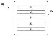
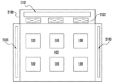
도 4 는 주입된 솔라 셀 실시예의 평면도(top view)이다. 도 4의 솔라 셀(500)은 선택적 에미터 디자인이나, 명세서에서 개시된 실시예들은 단순히 선택적 에미터 솔라 셀들에 한정되는 것은 아니다. 예를 들어, 솔라 셀(500)은 폭(width)과 높이(height)에서 약 156㎜ 또는 약 125mm일 수 있다. 도 1, 보다 상세하게는, 도 4 에 보여지는 것처럼, 솔라 셀(500)은 도핑된 컨택 영역들(501)을 가지며, 컨택 영역들(501) 사이의 에미터(502)는 컨택 영역들(501)보다 약간 저농도(lower) 도즈로 도핑된다. 일 예에서, 컨택 영역들은 약 5E15 도펀트 원자들/㎠로 도핑되고, 에미터(502)는 약 1E15 도펀트 원자들/㎠로 도핑된다. 다른 예에서, 컨택 영역들(501)은 약 2mm 떨어지고 폭이 약 100㎛ 이다. 이런 컨택 영역들(501)은 약 3E15로 도핑되고, 에미터(502)는 10keV 인(phosphorus) 주입을 이용하여 약 1.5E15로 도핑된다. 선택적 또는 패턴화된 주입은 컨택 영역들(501)을 도핑하는 반면, 솔라 셀(500)의 전체 표면위의 블랭킷(blanket)주입은 에미터(502) 도핑을 수행할 수 있다. 4 is a top view of an implanted solar cell embodiment. Although the
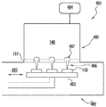
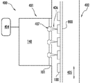
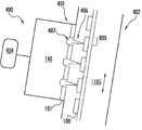
도 5 는 본 발명의 제 1 실시예에 일치하는 공정 장치들의 블럭도이다. 시스템(400)은 플라즈마 소스(401), 집속 플레이트(101)(또는 시스(sheath) 처리(engineering) 플레이트) 및 공정 챔버(402)를 포함한다. 가스 소스(404)는 플라즈마 소스(401)에 연결된다. 플라즈마 소스(401) 또는 시스템(400)의 다른 컴포넌트들은 터보 펌프와 같은 펌프(미도시)에 또한 연결될 수 있다. 플라즈마(140)을 생성하는 플라즈마 소스(401)은 예를 들어, RF 플라즈마 소스, 유도 결합 플라즈마(inductively-coupled plasma)(ICP) 소스, 방열 음극(indirectly heated cathode)(IHC) 또는 당업자들에 알려진 다른 플라즈마일 수 있다. 이 특정 실시예에서, 플라즈마 소스(401)는 RF 소스 제너레이터(408) 및 RF 소스 제너레이터(409)를 가진 RF 플라즈마 소스이다. 플라즈마 소스(401)은 인클로저(enclosure)(411)에 의해 둘러싸이고, 이 특정 실시예에서, DC 브레이크(410)는 인클로저(411)을 공정 챔버(412)로부터 분리한다. 공정 챔버(402), 플라즈마 소스(401) 또는 플래튼(403)은 접지(ground) 될 수 있다.5 is a block diagram of processing equipment in accordance with the first embodiment of the present invention. The
집속 플레이트(101)는 워크피스(100)에 주입을 위한 이온들(406)을 추출하기 위해 사용된다. 집속 플레이트(focusing plate)(101)은 냉각될 수 있다. 플라즈마 소스(401)로부터 플라즈마(140)의 추출(extraction)은 연속적(continuous)(DC) 또는 펄스화(pulse)될 수 있다. 플라즈마 소스(401)는 바이어스 될 수 있고, 바이어스 파워 서플라이(bias power supply)(미도시)는 이온들(406)을 끌어당기기 위해서 기판상에 연속적 또는 펄스화된 바이어스를 제공하기 위해서 제공될 수 있다. The
비록 복수(multiple)의 개구(407)들이 도 5에 예시되어 있으나, 집속 플레이트(101)는 적어도 한개 개구(407)를 가질 수 있다. 도 20에 대하여 이하에서 추가적으로 논의되는 것처럼, 개구들(407)은 워크피스(100)내에 소정의의 주입 패턴에 대응하는 어레이(array)에 배열될 수 있다. 집속 플레이트(101)는 냉각되거나 또는 그것의 열적 특징들을 제어하는 다른 방법일 수 있다. 플라즈마 소스(401) 및 공정 챔버(402)내의 압력은 거의 동일할 수 있고, 그것이 아크(arcing)을 야기할 수 있다. 다른 전기 포텐셜의 객체들(objects) 사이의 거리를 증가함으로써 그리고 가능하다면 컴포넌트들 상의 매끄러운 표면들을 채용함으로써 높은 전압 아크는 최소화될 수 있다는 것은 당업자들이 인식할 것이다. 워크피스(100)에 주입된 영역들의 치수(dimension)는 시스템(400)의 컴포넌트들의 파라미터들에 따라서 변할 수 있다.Although
솔라 셀들일 수 있는 하나이상의 워크피스들(100)은 공정 챔버(402)에 플래튼(403)상에 배열된다. 집속 플레이트(101)와 워크피스들(100) 사이의 거리는 집속 플레이트(101)의 임의 열적 팽창(thermal expansion)을 보상하기 위해 제어될 수 있다. 이러한 워크피스(100)들은 폭이 N 워크피스들(100)이고 길이가 N 워크피스들(100)(폭 치수에 "N" 변수는 길이 치수에 변수와는 상이할 수 있는)인 어레이 또는 매트릭스에 배열될 수 있다. 도 5에서, 1x3 워크피스들의 매트릭스 예시된다. 수직 방향으로 배열된 플래튼(403)은 워크피스(100)들을 유지하기 위해서 정전기 클램핑(electrostatic clamping), 기계적 클램핑(mechanical clamping) 또는 정전기 및 기계적 클램핑의 조합을 이용할 수 있다. 워크피스들(100)은 플래튼(403)을 이용하여 주사(scan)될 수 있다. 도 5의 실시예에서, 플래튼(403)은 방향(405)로 주사될 수 있다. 그러나, 플래튼(403)은 워크피스(100)들 상의 소정의의(desired) 주입 패턴에 기초하는 1D 또는 2D 주사(scanning)를 시행할 수 있다. 예를 들어, 워크피스들(100)에 스팟-모양(spot-shaped) 또는 점-모양(dot-shaped)의 주입 영역들을 생성하기 위해 2D 주사가 시행될 수 있다. 대안적인 실시예에서, 정지된 워크피스들(100)에 대하여 집속 플레이트(101)가 주사된다. 다양한 로드 및 언로드 메커니즘이 플래튼(403)상에 워크피스(100)들을 배치하는데 사용될 수 있다. 플래튼(403)은 일 예에서 워크피스들(100)을 냉각하는 백사이드(backside gas) 가스를 제공하도록 구성될 수 있다. 워크피스(100)는 플래튼(403) 또는 어떤 다른 장치들을 이용한 주입 전에 또는 주입 동안에 다양한 온도로 가열되거나 또는 냉각될 수 있다.One or
플라즈마 소스(401)의 펄싱(pulsing)은 집속 플레이트(101) 및/또는 워크피스들(100)의 주사(scanning)에 동기화될 수 있다. 주사는 워크피스들(100)을 가로질러서 이온들의 소정의의 도즈(dose) 및 분포(distribution)을 성취하기 위해 구성될 수 있다. 이온들(406)을 형성하기 위한 추출의 펄스화된 특징은 워크피스(100)의 더 나은 전하 중화(charge neutralization)를 가능하게 할 수 있다. 일 예에서 이차 전자(secondary electron) 제어 플레이트가 사용될 수 있다.Pulsing of the
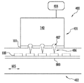
도 6 은 본 발명의 제 2 실시예에 일치하는 플라즈마 공정 장치들의 블럭도이다. 이 실시예에서, 플래튼(403)은 집속 플레이트(101) 아래에 배치될 수 있고, 방향(605)로 움직인다. 워크피스들(100)을 지지하기 위해서 중력의 이용이 플래튼(403)을 단순화할 수 있으나, 입자들(particles) 증착(deposition) 또는 입자들 낙하(falling)가 워크피스들 상에서 일어날 수 있다. 6 is a block diagram of plasma processing apparatuses in accordance with a second embodiment of the present invention. In this embodiment, the
도 7 은 본 발명의 제 3 실시예에 일치하는 플라즈마 공정 장치들의 블럭도이다. 이 실시예에서, 플래튼(403)은 집속 플레이트(101) 위에 배치되고, 방향(605)로 움직인다. 이것은 워크피스들(100)상의 입자들 또는 증착의 위험은 배제할 수 있으나, 플래튼(403)은 시스템(400)내에 공정 동안에 거꾸로 워크피스(100)들을 유지하기 위한 적절한 클램핑 힘(force)을 요구한다.7 is a block diagram of plasma processing apparatuses in accordance with a third embodiment of the present invention. In this embodiment, the
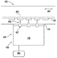
도 8 은 본 발명의 제 4 실시예에 일치하는 플라즈마 공정 장치들의 블럭도이다. 이 실시예에서 워크피스들(100)은 수직 방향일 수 있는 방향(405)로 움직이는 컨베이어 벨트(800) 상에 배치된다.8 is a block diagram of plasma processing apparatuses in accordance with a fourth embodiment of the present invention. In this embodiment the
도 9 는 본 발명의 제 5 실시예에 일치하는 플라즈마 공정 장치들의 블럭도이다. 워크피스들(100)은 수평 방향일 수 있는 방향(605)로 움직이는 컨베이어 벨트(800) 상에 배치된다. 이 시스템(400)은 도 6의 실시예에서와 유사하게 워크피스(100)상에 증착 또는 입자들을 가질 수 있다.9 is a block diagram of plasma processing apparatuses in accordance with a fifth embodiment of the present invention. The
도 10 은 본 발명의 제 6 실시예에 일치하는 플라즈마 공정 장치들의 블럭도이다. 워크피스들(100)은 방향(605)로 움직이는 컨베이어 벨트(800)상에 배치될 수 있다. 컨베이어 벨트(405)는 워크피스들(100)이 거꾸로 유지되게 하기 위해서 워크피스들(100)을 그립(grip)할 수 있다. 이 실시예는 워크피스들(100) 상의 증착 또는 입자들의 위험을 배제할 수 있다. 10 is a block diagram of plasma processing apparatuses in accordance with a sixth embodiment of the present invention. The
예를 들어, 도 5-10의 실시예들에서 컨베이어 벨트(800) 및 플래튼(403)이 예시되었으나, 다른 워크피스(100) 운송 메커니즘이 사용될 수 있다. 따라서, 명세서에서 개시된 실시예들은 컨베이어 벨트(800) 또는 플래튼(403)에 전적으로 한정되지 않는다. 컨베이어 벨트(800)를 이용하는 어떤 실시예들에서는 공정 챔버(402)에 진공(vacuum)을 유지하기 위해서 다양한 펌핑을 사용할 수 있다. For example, although the
도 11 은 본 발명의 제 7 실시예에 일치하는 플라즈마 공정 장치들의 블럭도이다. 이 실시예에서, 적어도 컨베이어 벨트(800) 및 집속 플레이트(101)는 경사지고(angled), 워크피스들(100)은 수평과 수직 사이의 범위에 각도일 수 있는 방향(1105)로 움직인다. 비록 도 11 의 실시예의 전체 시스템(400)은 경사지게 예시되고 있으나, 시스템(400)의 나머지는 경사지지 않을 수 있다. 비록 플래튼(403) 또는 다른 워크피스(100) 운송 메커니즘이 사용되고 있으나 컨베이어 벨트(800)이 예시된다. 경사진 구성(angled configuration)은 워크피스들의 중력 정렬을 허용하고 컨베이어 벨트(800) 상의 워크피스들을 유지하는 메커니즘을 단순화할 것이다.11 is a block diagram of plasma processing apparatuses in accordance with a seventh embodiment of the present invention. In this embodiment, at least the
도 12 는 본 발명의 제 8 실시예에 일치하는 플라즈마 공정 장치들의 블럭도이다. 시스템(1200)에서, 플라즈마 소스(401) 및 플라즈마 소스(1203)이 예시된다. 플라즈마 소스(1203)은 가스 소스(1202)로부터 플라즈마(1201)를 형성한다. 일 예에서, 플라즈마(140) 및 플라즈마(1201)은 이런 배열로 한정되는 것은 아니지만, 플라즈마(1201)는 p-타입이고, 즉, 워크피스들(100)에 p-타입 도펀트 종들을 공급하는 플라즈마이고, 플라즈마(140)는 n-타입이고 즉, 워크피스들(100)에 n-타입 도펀트 종들을 제공하는 플라즈마이다. 일 특정 실시예에서, 시스템(1200)은 도 2에서 예시된 것 처럼 IBC 솔라 셀들을 만들기 위해서 사용될 수 있다. 따라서, 플래튼(403)은 IBC 솔라 셀의 n-타입 및 p-타입 영역들을 도핑하기 위해서 플라즈마 소스(401) 및 플라즈마 소스(1203) 사이에서 워크피스들(100)을 병진시킨다(translate). 플라즈마 소스들(401,1203)은 주입 기간들 동안에 온(on) 및 오프(off) 될 수 있고 또는 워크피스들(100)에 어떤 카운터도핑(counterdoping) 효과를 가지도록 연속적으로 동작할 수 있다. 바이어스의 강도(strength)는 카운터 도핑 효과를 최소화하기 위해서 또한 조정될 수 있다. 다시 말하면, n-도핑을 의도하는 워크피스 영역들이 플라즈마(1201)에 노출될 때 뿐만 아니라 p-도핑을 의도하는 워크피스 영역들이 플라즈마(140)에 노출될 때 플라즈마와 워크피스 사이의 바이어스는 감소될 수 있다. 12 is a block diagram of plasma processing apparatuses in accordance with an eighth embodiment of the present invention. In
플래튼(403)이 예시되었으나, 컨베이어 벨트 또는 다른 워크피스(100) 운송 메커니즘이 사용될 수 있다. Although
도 22 는 본 발명의 제 9 실시예에 일치하는 플라즈마 공정 장치들의 블럭도이다. 시스템(2200)은 플라즈마 소스(401) 및 플라즈마 소스(2201)를 가진다. 플라즈마 소스(2201)는 가스 소스(2203)로부터 플라즈마(2202)를 형성한다. 플래튼(403)이 예시되었으나, 컨베이어 벨트 또는 다른 워크피스(100) 운송 메커니즘이 사용될 수 있다. 이 실시예에서 플래튼(403)은 플라즈마 소스(401) 및 플라즈마 소스(2201) 사이에서 회전 또는 트위스트(twist) 될 수 있다. 다른 실시예에서, 플래튼(403) 또는 어떤 다른 운송 메커니즘은 워크피스(100)들의 두개의 대향되는 측면들(sides) 상에 주입을 허용할 수 있다. 다른 실시예에서 플라즈마 소스(402) 및 플라즈마 소스(2201)는 상이한 앙각(elevation)에 있을 수 있다. 22 is a block diagram of plasma processing apparatuses in accordance with a ninth embodiment of the present invention.
도 12 및 도 22의 실시예들에서, 두개의 플라즈마 소스들이 예시되었다. 두개 이상의 플라즈마 소스들이 사용될 수 있다. 시스템들(1200, 2200)이 수직으로 예시되었으나, 명세서에서 개시된 다른 실시예들에서와 마찬가지로 다른 구성들이 가능하다. 블랭킷 및 선택적 주입, 도핑 및 물질 변형 주입들을 위해 사용된 두개의 플라즈마 소스들을 가진 다른 시스템들 또는 다른 구성들이 가능하다.In the embodiments of Figures 12 and 22, two plasma sources have been illustrated. Two or more plasma sources may be used. Although
명세서에서 개시된 실시예들에서, 플라즈마 소스(401)과 같은 플라즈마 소스는 연속적으로 동작할 수 있다. 이것이 플라즈마(140)를 생성하기 위해 필요로 하는 시간을 줄인다. 집속 플레이트(101)은 시스템(400)내에 제자리에서(in-situ) 세정될 수 있다. 일 예에서, 세정 플라즈마(cleaning plasma)는 플라즈마 소스(401)에서 운용될 수 있다.이 예방 유지(preventative maintenance)는 예를 들어, 어떤 다수의 주입 사이클 후에 수행될 수 있다. 증착을 일으키는 종(species)들이 플라즈마 소스(401)에 사용되는 시간 동안에 이 세정(cleaning)이 이온들(406)의 소정의의 특징들 또는 치수들을 유지할 수 있다. 집속 플레이트(101)의 열적 제어는 집속 플레이트(101) 상에 증착을 줄일 수 있다. 이것은 집속 플레이트의 가열(heating) 또는 냉각(cooling)을 포함할 수 있다. In the embodiments disclosed herein, a plasma source such as
본 발명의 플라즈마 공정 장치들의 실시예들은 복수의 마스크들 또는 복잡한 주입 계획(scheme)들의 요구 없이 선택적 작은 영역 및 블랭킷 주입 모두 용이하게 한다. 이것을 이루기 위해서, 개구(aperture) 및 워크피스 구성은 집속된 이온들의, 이온 빔이 형성되는 개구들보다 실질적으로 좁은 폭(개구 폭의 약 75%보다 작은 의미)의 영역에 기판을 수렴시키고 그리고 차단시키는 이온 빔 폭(width)을 형성하는, 추출(extraction)을 용이하게 하기 위해서 적절한 플라즈마 파라미터와 함께 디자인될 수 있다. Embodiments of the plasma processing apparatuses of the present invention facilitate both selective small area and blanket implantation without the need for multiple masks or complex implant schemes. To achieve this, the aperture and workpiece configuration converges and blocks the substrate in a region of focused ions that is substantially narrower in width (meaning less than about 75% of the opening width) of the apertures through which the ion beam is formed. It can be designed with appropriate plasma parameters to facilitate extraction, which creates an ion beam width.
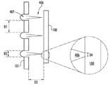
도 13 은 이온 집속(ion focusing)의 세부사항(details)을 예시하는 집속 플레이트의 일 실시예의 단면도이다. 집속 플레이트(101)는 개구들(407)을 약 1cm가 될 수 있는 거리 D1 간격으로 떨어 뜨릴 수 있다. 개구들(407)은 약 2mm의 길이 D2 일 수 있다.워크피스(100)는 집속 플레이트(101)로부터 약 1cm의 거리 D3 간격을 둘 수 있다. 집속 플레이트(101)을 이용한 워크피스에 주입 영역은 약 100㎛의 폭 D4 일 수 있다. 집속 플레이트(101)는 약 156mm보다 더 높은 개구들(407)을 가질 수 있다(도 13의 해당 페이지). 집속 플레이트(101) 그 자체는 156mm 보다 더 넓을 수 있다. 집속 플레이트(101)은 10keV 주입을 위한 각 개구(407)로부터 약 0.2A/m 의 이온들(406)을 추출할 수 있고, 만약 워크피스(100)가 집속 플레이트(101)로부터 약 1cm 떨어져 간격을 두고 있다면 이온들(406)은 워크피스(100)에 100㎛ 주입 폭 이하로 집속 될 수 있다. 만약 거기에 15 개구들(407)들이 있다면 이것은 워크피스(100) 위에 468mA의 이온(406) 전류와 동등한 것이다. 만약 길이 D2가 약 1mm 이고 플라즈마 소스가 5keV로 바이어스 되고, 워크피스(100)이 접지되었다면, 이온들(406)은 10배 이상까지 집속될 것이다. 따라서, 본 발명의 실시예들은 약 10㎛의 길이 D4를 가지는 주입 영역들을 위해서 사용 될 수 있다. 다른 집속 수준(level)들이 또한 가능하다. FIG. 13 is a cross-sectional view of one embodiment of a focusing plate illustrating details of ion focusing. FIG. The focusing
따라서, 본 발명의 실시예들은 밀리미터의 차수(order)에 개구 폭을 이용하여 수백 마이크론(micron)에 마이크론 차수(order)에 정지 주입 폭(stationary implant width)(집속 이온들에 관하여 워크피스를 주사(scanning)함이 없이 생산된 주입 영역의 폭 의미)을 생산할 수 있다. 좁은 선택적으로 주입된 영역들에 형성된 폭은 정지 주입 폭과 같거나 크다(주사(scanning)를 이용). 더욱이, 집속 이온들은 상대적으로 큰 개구 폭 D2로부터 추출되기 때문에, 집속된 이온들(406)은 워크피스(100)에 정지 주입 폭 D4 위에 높은 이온 플럭스(flux)(전류)(current)를 제공한다. 이것은 작은 영역들에 하이 도즈(high dose) 주입 뿐만 아니라 블랭킷 주입들의 요구되는 주입 수준들을 위한 적정한 워크피스 주사 율(scan rate)을 수용할 수 있는 충분히 높은 이온 전류(ion current)를 제공함으로써 빠른 블랭킷 주입을 용이하게 한다.Thus, embodiments of the present invention scan a workpiece in terms of stationary implant width (focused ions) in order of hundreds of microns using an aperture width in order of millimeters. can be produced without scanning. The width formed in the narrow selectively implanted regions is equal to or greater than the stationary implant width (using scanning). Moreover, because focused ions are extracted from a relatively large opening width D2,
도 14 는 본 발명의 방법에 따른 주입 동안에 스텝화된(stepped) 이동(movement)을 예시하는 단면도이다. 워크피스(100)는 방향(405)으로 이온들(406)에 대하여 움직인다. 이것은 워크피스(100)에 고농도 도핑된(higher-doped) 영역들(1400)와 저농도 도핑된(lower-doped) 영역들(1401)을 형성한다. 고농도 도핑된 영역들(1400)을 형성하기 위해서, 워크피스(100)는 저농도 도핑된 영역(1401)의 주입 동안 보다 플레이트(101)에 대하여 더 천천히 주사된다. 이런 공정이 워크피스(100)의 표면 상에 반복될 수 있다. 14 is a cross sectional view illustrating a movement stepped during injection in accordance with the method of the present invention.
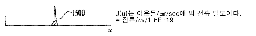
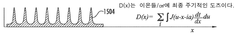
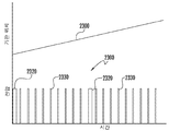
도 15a-15d로 돌아가서, 기판(100)에 수용된 이온 도즈(1504)와 집속 플레이트(101)과 기판(100) 사이에서 제공되는 다양한 주사 속도(scanning velocity)간의 관계(relationship)를 예시하기 위해서 세부사항(detail)들이 제공된다. 다양한 주사 속도(또는 율)는 정지 기판(100)에 대하여 집속 플레이트(101)를 주사함으로써, 정지 집속 플레이트(101)에 대하여 기판(100)을 주사함으로써, 또는 기판과 집속 플레이트를 동시에 주사함으로써 제공될 수 있다. 주입 동안에 주사 속도를 변화함으로써, 상대적으로 고농도(higher) 그리고 상대적으로 저농도(lower) 주입 수준의 영역들이 생산될 수 있다. 도 15a-15d 에 도시된 실시예에서, 방향 X에 기판 (100)을 따라서 위치의 함수로서 다양한 이온 도즈(1504)를 생산하기 위해 다양한 주사 율(scan rate)이 채용된다. 도 15a에 도시된 것처럼, 이온들(406)이 기판(100) 위에 부딪(impinge)칠 때 집속된 모양을 형성하기 위해 집속 플레이트(101)을 이용한 플라즈마(140)로부터 이온들이 추출된다. 이온들(406)이 기판(100)으로 주입될 때, 기판에 이온들의 전류 밀도(current density)(1500)는 도 15b에 보여지는 것일 수 있다. 도시된 것처럼, 1cm 폭 개구들(407)을 관통하여 추출된 이온들의 전류 밀도는 좁게 뾰족하게 되고, 이온들이 기판(100) 위에 부딪칠 때 이온들의 폭은 약 100㎛일 수 있다. Returning to FIGS. 15A-15D, details to illustrate the relationship between the
도 15c 는 집속 플레이트(101)을 위해 사용될 수 있는 단일 주사 율 시퀀스(sequence)(1502)을 도시한다. 이 실시예에서, 주사 율 시퀀스는 체류 시간(residence time)(sec/cm) 함수로 나타낼 수 있어서 체류 시간 함수(1504)에 피크들(1506)은 주사 율이 상대적으로 느린 영역들을 나타내고, 베이스 영역들(1508)은 주사 율이 상대적으로 빠른 영역들을 나타낸다. 따라서, 영역들(1506)에서는 집속 이온들(1500)이 영역들(1508)에서 보다 기판(100)을 가로질러서 상대적으로 더 천천히 주사되기 때문에 고동도 이온 도즈가 수용된다. 느린 주사 율과 빠른 주사 율간의 이 변화는 도 15c에 보여지는 것과 같이, 기판(100)에서 이온 도즈(1504)의 주기적 변화를 유도하여 그래서 X방향에 상대적으로 고농도 및 저농도 이온 도핑 영역을 생산하는 주기적 방식으로 반복될 수 있다.15C shows a single rate sequence sequence 1502 that can be used for the focusing
본 발명의 실시예들은 워크피스의 상이한 영역들에 도핑 수준들을 변화하기 위한 펄스화된 플라즈마 주입(pulsed plasma implantation)을 또한 채용할 수 있다. 대안적 실시예에서, 펄스화된 DC 또는 RF 주입의 경우에, 펄스 길이 또는 펄스 주파수는 고농도 도핑된 영역들(1400)을 형성하기 위해서 증가될 수 있다. 이런 대안적 실시예들에서, 워크피스(100)의 주사 율은 일정(constant)할 수 있으나 반면에 그것이 상대적으로 더 짧은 펄스들 또는 작은 펄스 율에 노출되는 영역(1401)들 보다 더 고농도로 도핑되는 영역들(1400)상에 이온들(406)이 부딪칠 때는 펄스화된 플라즈마의 펄스 율 (또는 길이)은 상대적으로 크게 만들어진다.Embodiments of the present invention may also employ pulsed plasma implantation to vary doping levels in different regions of the workpiece. In an alternative embodiment, in the case of pulsed DC or RF injection, the pulse length or pulse frequency may be increased to form heavily doped
본 발명의 실시예들에서, 도 5에 개시된 것과 같은 장치들은 워크피스들을 주입하기 위해 사용될 수 있어서 펄스화된 이온 주입 공정과 관련된 파라미터들은 소정의의 도핑 수준에 따라서 변화될 수 있다. 이러한 파라미터들은 펄스 지속기간(pulse duration), 펄스 주파수(pulse frequency), 및 소스와 기판 펄스들의 동기화(synchronization)을 포함할 수 있다. 펄싱(pulsing)의 예제들은 플라즈마에 펄스화된 포텐셜(potential)을 적용하는 것 또는 워크피스에 펄스화된 포텐셜을 적용하는 것을 포함한다.In embodiments of the present invention, devices such as those disclosed in FIG. 5 may be used to implant the workpieces so that the parameters associated with the pulsed ion implantation process may vary depending on the desired doping level. Such parameters may include pulse duration, pulse frequency, and synchronization of source and substrate pulses. Examples of pulsing include applying a pulsed potential to a plasma or applying a pulsed potential to a workpiece.
도 18 - 19 는 각각 RF 또는 DC 동기화(synchronization)가 워크피스를 복수의 상이한 도펀트 수준으로 주입하기 위해 사용되는 본 발명의 방법들에 관여된 대표적인 단계들을 예시한다.물론, 도18-19에 예시된 것과 다른 방법들이 가능하다. 양자 방법들에서, 주기적인 주입 펄스가 생성되는 동안에 타겟(1800)은 개구 플레이트(101)과 같은 개구 플레이트(aperture plate)에 대하여 주사될 수 있다. 도 18 및 19의 실시예들에 따라서, 플라즈마(140)로부터 파저티브 이온들이 집속 플레이트(101)를 관통하여 워크피스(100)상으로 가속되도록 하기 위해서 주입 펄스의 "온(on)" 기간 동안에 네거티브 포텐셜과 같은 포텐셜이 워크피스와 플라즈마 사이에 적용될 수 있다. 18-19 illustrate representative steps involved in the methods of the present invention where RF or DC synchronization is used to inject a workpiece into a plurality of different dopant levels, respectively. Other methods are possible. In both methods, the
본 발명의 특정 실시예에서, 주지의 기술들에 따라 플라즈마(140)는 플라즈마 펄스 소스에 의해 펄스화된 방식으로 생성될 수 있다. 특별히, 펄스화된 플라즈마는 워크피스(100)에 바이어스를 적용할 필요없이 컴포넌트(미도시)를 이용하여 생성될 수 있다. 원하는 때에, 주입 펄스들이 소스 펄스들에 일반적으로 일치하도록 하기 위해서 주입 펄스들은 주기적으로 생성될 수 있다. 따라서, 주입 펄스들이 생성 되었을때, 플라즈마(140)가 또한 "온(on)" 이고, 플라즈마(140)으로부터 이온들이 주입 펄스에 의해 워크피스에 가속되고 워크피스(100)에 주입된다. 기판의 다른 영역들에 다른 도펀트 수준들을 성취하기 위해서, 주입 펄스들은 상이하게 동기화될 수 있다. In a particular embodiment of the invention, the
도 18에 특별히 돌아가서, 하이 도즈 및 로우 도즈 영역들에 대응하는 워크피스에 두개의 다른 도핑 수준들의 영역들을 생성하기 위해 거기에 예시된 방법이 채용될 수 있다. 그 방법은 개구 플레이트(101)에 대하여 타겟(100)을 주사하기 위해서, 타겟(워크피스(100))에 하나이상의 상대적으로 고농도 도핑 수준 영역들 및 하나이상의 상대적으로 저농도 도핑 수준 영역들을 생성하기 위해서 사용될 수 있다. step 1800에서, 소스 펄스 타이밍이 생성된다. 예를 들어, 이온 주입 시스템에 연결된 펄스 제너레이터는 매 펄스마다 50㎲의 지속기간(duration) ![]()
![]()
step 1802에서, 주어진 영역에 하이 이온 도즈 또는 로우 도즈가 적용될 것인지에 관한 결정이 만들어진다. 예를 들어, 개구들을 관통하여 가속된 이온들을 이용하여 로우 이온 도즈 영역들이 형성되기를 의도한 집속 플레이트(101)에 대하여 워크피스는 최초 지점에 위치될 수 있다. 따라서, 전류 워크피스 위치와 적용될 소정의 로우 도즈 주입을 서로 관련시키는 프로세서에 의해 프로그램 또는 명령들의 셋(set)이 실행될 수 있다. In
step 1804 및 1806에서, 로우 또는 하이 이온 도즈 수준들에 대응하는 매(every) i 또는 j 펄스들을 위해서 대응하는 엔코더 펄스들이 생성된다. 예를 들어, 로우 도즈(1804) 경우를 위해서, 엔코더 펄스는 매(every) 200㎲에 대응하는 매(every) 2 소스 펄스들을 생성되게 할 수 있고 반면에 하이 도즈(1806) 경우를 위해서, 엔코더 펄스는 매(every) 1000㎲에 대응하는 매(every) 20 소스 펄스들을 생성되게 할 수 있다. In
일 실시예에서, step 1808에 보여지는 것과 같이 모터 엔코더 카운터가 증분될 때까지 워크피스(100)는 정지상태를 유지할 수 있고, step 1810에 보여지는 것과 같이 주사 시스템 모터는 이동하는 메시지를 전송한다. 워크피스는 엔코더 펄스들 사이에서 정지될 수 있고, 따라서, 로우 도즈 경우에 워크피스(100)에 주입은 플라즈마(140)가 온 상태인 동안에 2개의 소스 펄스들로 구성된다. 이 주입 방안(recipe)은 워크피스(100)이 이동 전에 10개 소스 펄스들이 주입되는 하이 도즈 경우에 대조된다. 5배만큼 많은 주입 펄스들에 노출되기 때문에 고농도 도즈 영역(higher dose region)은 따라서 저농도 도즈 영역의 도즈를 5배 수용한다.In one embodiment, the
도 19는 워크피스 상에 상이한 영역들에 대하여 임의의 다수의 다른 도핑 수준들을 성취하기 위한 동기화를 적용하기 위해 사용되는 방법을 제외하고는 도 18의 방법에 유사한 방법을 도시한다. 그 방법은 주입되는 영역들에 대응하는 적절한 이온 주입 도즈가 결정되는 step 1800 및 step 1902에 따라서 진행한다. 일단 이것이 결정되면, 주입될 결정될 도즈 수준에 대응하는 대안적인 단계들(1904-1908에 보여진) 중 하나를 진행하여서, 적절한 엔코더 펄스 시퀀스가 생성된다. 다시, 소정의 도핑 수준에 따라서 소정 영역이 주입될때까지 워크피스(100)이 주사할때 엔코더 펄스 시퀀스는 적용될 수 있다. 도 18에서 처럼, 도 19의 방법은 소정의 도핑 수준에 따라서 발생되는 각각 1, 2, 3 등등의 소스 펄스들에 대해 엔코더 펄스들을 생성하는 것을 포함한다.FIG. 19 shows a method similar to the method of FIG. 18 except for the method used to apply synchronization to achieve any of a number of different doping levels for different regions on the workpiece. The method proceeds according to
다른 실시예에서, 워크피스(100)가 주사될 때 워크피스(100)에 도즈 제어를 위해서 펄싱 RF 또는 펄싱 DC가 사용될 수 있다. 이 펄싱은 마이크로세컨드 시간 규모(scale) 일 수 있다. 예를 들어, 펄스 지속기간 ![]()
![]()
그러나 다른 실시예에서, 워크피스(100)는 도 14에 예시된 방향(405)으로 일정한 속도로 주사되나,펄스 지속기간 또는 펄스 율은 고농도 도핑된 영역들(1400)을 형성하기 위해 증가될 수 있다. 예를 들어, 저농도 도핑된 영역들(1401)을 위한 주입에 비교된 5배 더 긴 펄스 또는 5배 더 빈번한(frequent) 펄스 율은 고농도 도핑된 영역들(1400)에 5배 도즈를 생성할 것이다. RF 및 DC 소스 펄싱이 둘 다 이용될 수 있다. 이것은 DC 펄스 동안에 RF 소스의 듀티 사이클(duty cycle)을 변형함으로써 또는 DC 펄싱 동안에 RF 소스의 파워 수준을 변형함으로써 수행될 수 이다. However, in another embodiment, the
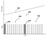
도 23-24 는 펄스화된 주입 시스템에 적용될 수 있는 대표적인 전압 커브들(2300 및 2400)을 시간의 함수로서 각각 보여준다. 위에서 서술한 것처럼, 전압 펄스들은 주입 펄스들 또는 소스 펄스들을 나타낼 수 있다. 워크피스 위치 커브들(2310 및 2410)이 각각 시간의 함수로서 도 23 및 24에 또한 보여진다. 도 23에서, 워크피스는 일정한 속도로 움직이나 워크피스에 고농도 도즈 영역들은 펄스(2320)와 같은 긴 펄스 지속기간에 의해 생성된다. 워크피스에 저농도 도즈 영역들은 펄스들(2330)와 같은 짧은 펄스 지속기간에 의해 생성된다.23-24 show
도 24에서, 워크피스는 다시 직선 커브(2410)에 의해 예시된 일정한 속도로 움직인다. 워크피스에 고농도 도즈 영역들(2420)은 높은 펄스 율에 의해 생성되고, 저농도 도즈 영역들(2430)은 낮은 펄스 율에 의해 생성된다. 도 23-24의 양자 실시예들에서, 저농도 도즈 영역들은 예를 들어, 솔라 셀에 컨택(contact)들 사이의 영역일 수 있고, 고농도 도즈 영역들은 예를 들어, 솔라 셀의 컨택들 아래에 영역들일 수 있다. In FIG. 24, the workpiece again moves at a constant speed, illustrated by
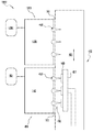
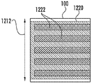
도 20a-c는 블랭킷(blanket) 및 선택적 주입을 수행하기 위해 구성된 집속 플레이트 시스템(1210)의 정면도를 나타낸다. 도 20a 및 20b에 예시된 것처럼, 워크피스(100)은 방향(1204)로 주사된다. 집속 플레이트 시스템(1210)의 실시예는 제 1 개구(1202)를 가진 제 1 집속 플레이트(1200)를 포함한다. 제 1 개구(1202)는 도 20c에 보여지는 것처럼 예를 들어,블랭킷 영역(1220)을 형성하기 위해서 방향(1204)로 주사함으로써 워크피스(100)의 폭을 가로질러서 블랭킷 주입을 수행할 수 있다. 제 2 집속 플레이트(1201)은 제 2 개구들(1203)을 가진다. 이런 제 2 개구들(1203)은 예를 들어 패턴화된 영역들(1222)을 형성하기 위해서 동일 방향(1204)로 개구들(1203)을 주사함으로써 워크피스(100)의 패턴화된 또는 선택적인 주입을 수행할 수 있다. 이 문맥(context)에서 주사(scanning)는 개구들(1202 및 1203)에 대하여 워크피스(100)의 상대적 움직임을 나타내고 워크피스(100) 및 집속 플레이들(1200 및 1201)중 어느 하나 또는 양자를 움직임으로서 성취될 수 있다. 두개 집속 플레이트가 도 20a-b의 실시예에 예시되었지만, 본 발명은 제 1 개구(1202) 및 제 2 개구들(1203) 양자를 가질 수 있는 단일의 집속 플레이트를 포함한다. 예시된 예제에서, 집속 플레이트들(1200 및 1201)은 지점 A 와 B사이의 거리에 동등한 거리를 방향 (1204)을 따라서 주사될 수 있다. 도 20b는 주사(scanning)가 완성된 후에 집속 플레이트들(1200 및 1201)의 상대적 위치를 도시한다. 패턴화된 영역들(1222)은 주사 거리를 원하는 만큼 증가함으로써 워크피스(100)의 가장자리들에 모든 쪽(way)으로 확장될 수 있다. 도 20a 에서의 최초 위치 및 도 20b 에서의 최종 위치를 가지는 집속 플레이트들을 위해 일어나는 주사(scanning) 후에 워크피스(100)의 주입 구조(geometry)의 세부사항을 도 20c는 예시한다. 주사 방향(1204)에 수직한 방향(1212)을 따라서, 제 2 개구들(1203)이 제 1 개구(1202)의 영역과 중첩되기 때문에, 제 2 개구들(1203) 아래에 노출된 주입된 영역들(1222)은 고농도 이온 도즈를 수용한다. 20A-C show a front view of a focusing
본 발명에 따른, 이러한 블랭킷 및 선택적 주입들은 도 20d-e에 예시된 것처럼, 적어도 부분적으로 동시될 수 있다. 도 20d는 개구(1202) 및 개구들(1203)이 동일한 플레이트에 포함된 집속 플레이트 시스템(1210)의 실시예를 도시한다. 도 20d에 보여지는 것처럼, 집속 플레이트(1210)는 방향(1204)을 따라서 왼쪽으로부터 지점(C)까지 주사될 수 있다. 도 20d에 예시된 구성은 플레이트(1210)이 워크피스(100)에 대하여 왼쪽으로 계속 움직인 후에 주입 주사의 중간에 지점을 표시할 수 있다. 도 20e는 도 20d에 의해 표시되는 지점까지 플레이트(1210)에 의해 생산되는 이온 주입의 패턴을 도시한다. 따라서, 지점C에 블랭킷 집속 개구(1202)의 리딩 에지에 대응하는 리딩 에지(1230a)를 가지는 블랭킷 영역들(1230)이 형성된다. 주사가 계속되기 때문에, 블랭킷 영역들(1230)은 도 20c 에 도시된 상황과 유사하게 전체 워크피스(100)를 가로질러서 확대될 수 있다. 도 20e는 선택적으로 주입된 영역들(1232)이 개구들(1203)을 이용하여 적어도 부분적으로 이미 형성된 것을 또한 예시한다. 거기다가, 점들, 스팟들(spots) 또는 다른 모양 주입하는 것들과 같은 집속 플레이트 개구들의 다른 배열(arrangements)이 가능하다. 이런 방식으로, 개구들은 소정의 주입 구조(geometry)와 관련된 둥글고, 타원형의(oval) 또는 다른 모양을 가질 수 있다. In accordance with the present invention, such blankets and selective implants may be at least partially simultaneous, as illustrated in FIGS. 20D-E. 20D shows an embodiment of a focusing
도 21 는 공정 제어 장치의 정면 사시도(front perspective view)이다. 공정 제어 장치(2100)는 이 실시예에서, 워크피스(100) 및 플래튼 (403) 위 또는 근처에 배치된다. 이 공정 제어 장치들(2100)은 이온 플럭스(flux), 집속 플레이트를 떠나는 이온들의 치수(dimension) 또는 확산(spread), 이온들의 위치(locations) 또는 워크피스(100)에 대하여 어떻게 평행한지를 측정하기 위해서 구성될 수 있다. 제 1 개구(2101)은 이온들의 긴 치수(long dimension)보다 더 긴 치수를 가진다. 자기적으로 또는 전기적으로 억제될 수 있는 패러데이 컵(미도시)이 전체 이온 측정을 위해 제 1 개구(2101)뒤에 배치될 수 있다. 제 1 개구(2101)들에 의해 형성되는 영역은 수평 이온 균일성(uniformity)을 결정하기 위해서 분할 될 수 있다. 개구 어레이(2102)들은 오프셋(offset) 개구들의 칼럼들을 포함한다. 개구 어레이들(2102)에 각 개구는 이온들의 기대 폭(width)보다 약 10배 작다. 자기적으로 또는 전기적으로 억제될 수 있는 패러데이 컵(미도시)은 각 개구 어레이(2102) 뒤에 배치될 수 있다. 수평 방향에 대하여 분리된 어레이들의 추가적인 셋들(set)은 폭 또는 평행 관계(parallelism)에 변화에 대한 정보를 준다. 공정 제어 장치들(2100)의 영역들은 광학적으로 모니터 될 수 있는 이온 빔에 의해 부딪칠 때 발광(luminescence)을 증가시키는 물질로 코팅될 수 있다. 실시간 도즈 측정을 제공하기 위해서 및 주사 속도 보정을 위해 사용될 수 있는 제 2 개구들(2103)은 플래튼(403)의 주변(periphery)에 배치될 수 있다. 분할될 수 있는 억제된 패러데이 컵(미도시)은 각 제 2 개구(2103)뒤에 배치될 수 있다. 21 is a front perspective view of the process control device.
이 시스템의 실시예들을 이용하여 이차 전자들(secondary electrons)이 생성될 수 있다. 워크피스(100)의 차징(charging)은 이온들(406)내 이온들의 궤적들(trajectories)에 영향을 줄 수 있다. 집속 플레이트(101)의 초점(focus)이 영향을 받을 수 있고, 집속 플레이트(101)의 에칭이 일어날 수 있고, 집속 플레이트(101)의 가열은 이차 전자들 때문에 증가될 수 있다. 이차 전자들은 워크피스(100)보다 낮은 포텐셜에 주로 투명 전극(transparent electrode)에 의해 또는 워크피스(100) 뒤에 자석들(magnet)에 의해 억제될 수 있다. 도 16 는 정전기 억제(electrostatic suppression)의 일 실시예를 예시하는 단면도이다. 절연체, 도체 도는 절연 및 전도 층들의 조합일 수 있는 적어도 하나의 억제 플레이트(suppression plate)(1600)는 집속 플레이트(100) 상에 배치된다. 도 17a-b 는 자기 억제(magnetic suppression)의 두개 실시예를 예시하는 단면도이다. 각각 반대 극성(polarity)을 가질 수 있는 자석들(1700,1701)이 워크피스(100)(도 17a)뒤에 또는 집속 플레이트(101)와 임의의 이차전지에 영향을 미치는 워크피스(도 17b) 사이에 배치될 수 있다. 도 17a에서 자석들(1700,1701)은 플라즈마 소스에 대하여 정지 또는 움직일 수 있다. 도 17b에서 자석들(1700,1701)은 집속 플레이트(101)위에 또는 적어도 부분적으로 집속 플레이트 내에 배치될 수 있다. 도 17b에 자석들은 정지될 수 있고, 동작이 단순화된다. Secondary electrons can be generated using embodiments of this system. Charging the
명세서에 개시된 실시예들은 워크피스(100) 결정질 격자(crystal lattice)를 도핑 또는 변형하기 위해서 사용될 수 있다. 일 예에서, 수소(hydrogen) 및/또는 헬륨(helium) 주입은 워크피스(100)의 클리빙(cleaving)을 가능하게 하기 위해서 수행되어 워크피스(100)를 가로질러서 수소 및/또는 헬륨의 여러가지 도즈를 포함할 수 있다. 비정질화(amorphization)와 같은, 다른 물질 변형이 또한 수행될 수 있다. 명세서에서 개시된 실시예들을 이용한 주입은 반도체 또는 다른 응용들에 적용될 수 있다.Embodiments disclosed herein may be used to dope or modify the
본 발명은 명세서에서 서술된 특정 실시예들에 의한 범위에 한정되지 않는다. 실제로, 명세서에서 서술된 실시예들에 추가하여 본 발명의 다른 다양한 실시예들 및 본 발명에 대한 변형들은 앞에서의 서술 및 결합한 도면들로부터 당업자에게 자명할 것이다. 따라서, 이런 다른 실시예들 및 변형들은 본 발명의 범위내에 해당함을 의미한다. 추가적으로, 비록 본 발명은 특정 목적을 위해 특정 환경에서 특정 이행의 내용으로 명세서에서 서술되었지만, 당업자는 그것의 이용이 그것에 한정되지 않고 본 발명은 임의의 많은 목적을 위해 임의의 많은 환경하에서 유리하게 시행될 수 있음을 인식할 것이다. 바람직하게는, 이하에서 개시된 청구항들은 명세서에서 서술된 본 발명의 모든 범위 및 사상(spirit)의 관점에서 이해되어야 한다. The invention is not to be limited in scope by the specific embodiments described in the specification. Indeed, other various embodiments of the invention and variations to the invention in addition to the embodiments described in the specification will be apparent to those skilled in the art from the foregoing description and combined drawings. Accordingly, such other embodiments and modifications are meant to fall within the scope of the present invention. In addition, although the present invention has been described in the specification for the specific purpose in the context of a particular implementation, those skilled in the art are not limited to its use and the invention is advantageously implemented in any number of environments for any number of purposes. It will be appreciated. Preferably, the claims set out below should be understood in view of the full scope and spirit of the invention described in the specification.
Claims (25)
집속 플레이트(focusing plate) 근처의 플라즈마 시스(plasma sheath)의 모양을 변형하기 위해 구성된 개구(aperture)를 가져서 집속된(focused) 이온들을 정의하기 위해 이온들이 상기 개구를 빠져나가는 상기 집속 플레이트; 및
상기 집속된 이온들이 상기 개구보다 실질적으로 좁은 주입 폭을 가지며 상기 집속 플레이트로부터 분리된 워크피스(workpiece)를 포함하고, 주입동안에 상기 워크피스를 주사(scanning)함으로써 상기 워크피스에 복수개의 패턴화된 영역들을 생성하도록 구성된 공정 챔버(processing chamber);를 포함하는, 공정 장치.A plasma source configured to produce a plasma in a plasma chamber containing ions for implantation into a workpiece;
The focusing plate having an aperture configured to modify the shape of a plasma sheath near a focusing plate so that ions exit the opening to define focused ions; And
Wherein the focused ions have an implant width substantially narrower than the opening and include a workpiece separated from the focusing plate, wherein the plurality of patterned portions of the workpiece are scanned by scanning the workpiece during implantation. And a processing chamber configured to create regions.
상기 집속 플레이트는 복수개의 개구들을 포함하는, 공정 장치.The method according to claim 1,
And the focusing plate comprises a plurality of openings.
상기 복수개의 개구들은 상기 워크피스가 제 1 방향을 따라서 주사 될때 상기 워크피스의 블랭킷 주입(blanket implantation) 및 선택 영역들에 주입을 생산하기 위해 구성된 블랭킷 개구 및 한 셋(set)의 선택 개구들을 포함하는, 공정 장치.The method of claim 2,
The plurality of openings includes a blanket opening and a set of selection openings configured to produce blanket implantation of the workpiece and injection into the selection areas when the workpiece is scanned along the first direction. Process equipment.
두개 방향들로 상기 워크피스를 주사하기 위해서 구성된 워크피스 홀더;를 더 포함하는, 공정 장치.The method according to claim 1,
And a workpiece holder configured to scan the workpiece in two directions.
상기 워크피스 홀더는 수평 홀더(horizontal holder), 수직 홀더(vertical holder), 경사진(angled) 홀더 및 뒤집어진(upside down) 홀더 중 하나를 포함하는, 공정 장치.The method of claim 4,
And the workpiece holder comprises one of a horizontal holder, a vertical holder, an angled holder, and an upside down holder.
상기 개구들은 약 0.5mm 부터 5mm 까지의 폭을 가지고, 상기 주입 폭은 약 5㎛ 부터 약 2mm 까지 인, 공정 시스템.The method according to claim 1,
The openings have a width from about 0.5 mm to 5 mm, and the injection width is from about 5 μm to about 2 mm.
소정의 주사에서 상기 워크피스의 제 1 방향을 따라서 다양한 주사 율로 주사하도록 구성된 워크피스 홀더를 더 포함하여, 적어도 하나의 상기 복수개의 패턴화된 영역들을 형성하기 위해 상기 제 1 방향으로 주사한 후에 복수개의 주입된 영역들의 상이한 이온 주입 수준(level)들이 형성되는 , 공정 장치.The method according to claim 1,
The workpiece holder further comprises a workpiece holder configured to scan at various scan rates along the first direction of the workpiece in a predetermined scan, after the scan in the first direction to form at least one of the plurality of patterned regions. Different ion implantation levels of the two implanted regions are formed.
상기 플라즈마의 상기 이온들은 도펀트 종들과 관련되고, 상기 제 1 방향의 주사(scanning) 후에 복수개의 상이한 도펀트 농도(concentration)의 주입된 영역들이 형성되는, 공정 장치.The method of claim 7,
The ions of the plasma are associated with dopant species, and a plurality of implanted regions of different dopant concentrations are formed after the scanning in the first direction.
상기 플라즈마 소스는 펄스화된(pulsed) 플라즈마를 생산하기 위해서 구성되는, 공정 장치.The method according to claim 1,
The plasma source is configured to produce a pulsed plasma.
상기 장치는 상기 워크피스에 펄스화된 바이어스를 공급하도록 구성되는, 공정 장치.The method according to claim 1,
The apparatus is configured to supply a pulsed bias to the workpiece.
상기 장치는 상기 플라즈마에 펄스화된 바이어스를 공급하도록 구성되는, 공정 장치.The method according to claim 1,
The apparatus is configured to supply a pulsed bias to the plasma.
상기 개구는 상기 워크피스에 적어도 하나의 상기 다수개의 패턴화된 영역들을 위한 소정의 주입 패턴에 대응하는 어레이(array)를 포함하는, 공정 장치.The method according to claim 1,
And the opening includes an array corresponding to a predetermined implant pattern for at least one of the plurality of patterned regions in the workpiece.
상기 플라즈마 챔버에 상기 이온들이 제 1 타입의 이온 종(species)인 경우, 상기 장치는,
워크피스 홀더;
제 2 플라즈마 소스;
제 2 집속 플레이트(focusing plate) 근처의 플라즈마 시스(plasma sheath)의 모양을 변형하기 위해 구성된 개구(aperture)를 가져서 집속된(focused) 이온들을 정의하기 위해 이온들이 상기 개구를 빠져나가는 상기 제 2 집속 플레이트; 및
제 2 타입의 이온 종(species)을 공급하도록 구성되고 상기 제 2 플라즈마 소스에 연결되는 제 2 공정 챔버(processing chamber);를 더 포함하고,
상기 워크피스 홀더는 상기 워크피스를 상기 제 1 타입 이온 종 및 상기 제 2 타입 이온 종에 대응하는 각각의 제 1 및 제 2 영역들로 선택적으로 주입하기 위해서 상기 집속 플레이트 및 상기 제 2 집속 플레이트 아래에 주사하도록 구성된, 공정 장치.The method according to claim 1,
If the ions in the plasma chamber are of a first type of ion species, the apparatus is:
Workpiece holder;
A second plasma source;
The second focusing ions exiting the opening to define focused ions with an aperture configured to modify the shape of the plasma sheath near the second focusing plate plate; And
And a second processing chamber configured to supply a second type of ion species and coupled to the second plasma source.
The workpiece holder is below the focusing plate and the second focusing plate to selectively implant the workpiece into respective first and second regions corresponding to the first type ion species and the second type ion species. And a processing apparatus, configured to scan.
상기 제 1 타입 이온 종은 n-타입 도펀트들이고 상기 제 2 타입 이온 종은 p-타입 도펀트들인, 공정 장치.The method according to claim 14,
Wherein the first type ion species are n-type dopants and the second type ion species are p-type dopants.
상기 워크피스 홀더 상에 또는 근처에 배치된 공정 제어 장치, 개구 배열 및 실시간으로 이온 도즈를 측정하기 위해 구성된 검출기(detector)를 더 포함하는, 공정 장치.The method according to claim 5,
And a process control device disposed on or near the workpiece holder, an aperture arrangement, and a detector configured to measure ion doses in real time.
상기 제 1 타입 이온 종은 n-타입 도펀트들이고 상기 제 2 타입 이온 종은 p-타입 도펀트들인, 공정 장치.The method according to claim 14,
Wherein the first type ion species are n-type dopants and the second type ion species are p-type dopants.
워크피스 홀더 상에 배치된 상기 워크피스, 상기 워크피스에 대하여 상기 집속된 이온들을 끌어당기기 위해서 상기 워크피스 홀더 및 상기 플라즈마 사이에 바이어스를 제공하는 단계; 및
상기 워크피스에 복수개의 선택적으로 주입된 영역들을 생산하기 위해서 상기 집속 플레이트에 대하여 상기 워크피스를 주사하는 단계;를 포함한, 워크피스 주입 방법.Providing a focusing plate adjacent to a plasma chamber containing a plasma and configured to extract ions from the plasma through at least one opening providing focused ions to a workpiece ;
Providing a bias between the workpiece holder and the plasma to attract the focused ions to the workpiece, the workpiece disposed on the workpiece holder; And
And scanning the workpiece against the focusing plate to produce a plurality of selectively implanted regions in the workpiece.
상기 집속 플레이트는 블랭킷 개구(blanket aperture) 및 한 셋(set)의 선택 개구들을 포함하고, 단일 주사로 상기 워크피스를 주사하는 것은 제 1 이온 도즈에 상기 워크피스의 블랭킷 주입과 제 2 고농도 도즈에 한 셋의 상기 워크피스 영역들의 선택적 주입을 생산하는, 워크피스 주입 방법.The method according to claim 17,
The focusing plate includes a blanket aperture and a set of select openings, and scanning the workpiece in a single scan involves blanket injection of the workpiece into a first ion dose and a second high concentration dose. A method of implanting a workpiece, producing a selective implantation of a set of said workpiece regions.
상기 플라즈마에 제 1 펄스 주파수를 가지는 소스 펄스들을 공급하는 단계;
상기 집속 플레이트의 개구가 상기 워크피스의 제 1 영역 위에 위치할 때, 제 1 바이어스 펄스 주파수를 가지는 제 1 셋(set)의 바이어스 펄스들을 제공하는 단계로서 상기 제 1 셋의 바이어스 펄스들은 상기 소스 펄스들에 동기화되는 상기 제 1 셋의 바이어스 펄스들을 제공하는 단계; 및
상기 집속 플레이트의 개구가 상기 워크피스의 제 2 영역 위에 위치할때, 상기 제 1 바이어스 펄스 주파수와 다른 제 2 바이어스 펄스 주파수를 가지는 제 2 셋(set)의 바이어스 펄스들을 제공하는 단계로서 상기 제 2 셋의 바이어스 펄스들은 상기 소스 펄스들에 동기화되는 상기 제 2 셋의 바이어스 펄스들을 제공하는 단계;를 더 포함하는, 워크피스 주입 방법.The method according to claim 17,
Supplying source pulses having a first pulse frequency to the plasma;
When the opening of the focusing plate is located above the first region of the workpiece, providing a first set of bias pulses having a first bias pulse frequency, the first set of bias pulses being the source pulse. Providing the first set of bias pulses that are synchronized to the controllers; And
Providing a second set of bias pulses having a second bias pulse frequency that is different from the first bias pulse frequency when the opening of the focusing plate is located above the second region of the workpiece. And providing the second set of bias pulses synchronized with the set of bias pulses to the source pulses.
상기 워크피스 주사는 제 1 주사 율로 상기 워크피스의 제 1 영역을 주사하는 것과 제 2 고주사 율로 상기 워크피스의 제 2 영역을 주사하는 것을 포함하는, 워크피스 주입 방법.The method according to claim 17,
And said workpiece scanning comprises scanning a first area of said workpiece at a first scanning rate and scanning a second area of said workpiece at a second high scanning rate.
상기 워크피스 주사는 펄스들이 제 1 펄스 율로 상기 플라즈마에 제공되는 동안 제 1 영역을 주사하고, 펄스들이 제 2 고펄스 율로 상기 플라즈마에 제공되는 동안 제 2 영역을 주사하는 것을 포함하는, 워크피스 주입 방법.The method according to claim 17,
The workpiece scan comprises scanning a first region while pulses are provided to the plasma at a first pulse rate, and scanning a second region while pulses are provided to the plasma at a second high pulse rate Way.
상기 워크피스 주사는 펄스들이 제 1 펄스 지속기간(duration)으로 상기 플라즈마에 제공되는 동안 제 1 영역을 주사하고, 펄스들이 제 2 펄스 지속기간으로 상기 플라즈마에 제공되는 동안 제 2 영역을 주사하는 것을 포함하는, 워크피스 주입 방법.The method according to claim 17,
The workpiece scan scans the first region while pulses are provided to the plasma with a first pulse duration, and scans the second region while pulses are provided to the plasma with a second pulse duration. Including a workpiece injection method.
P-타입 도펀트 이온들을 가지는 제 2 플라즈마를 포함하는 제 2 플라즈마 챔버에 인접한 제 2 집속 플레이트를 제공하는 단계로서, 상기 제 2 집속 플레이트는 상기 워크피스에 대하여 집속된(focused) 이온들을 제공하는 적어도 하나의 개구를 관통하여 상기 플라즈마로부터 이온들을 추출하도록 구성된 상기 제 2 집속 플레이트를 제공하는 단계; 및
바이어스가 상기 워크피스와 상기 제 1 및 제 2 플라즈마 사이에 각각 적용되는 동안 상기 제 1 및 상기 제 2 집속 플레이트에 대하여 상기 워크피스를 주사하는 단계로서, 상기 워크피스에 한 셋(set)의 선택적으로 N-도핑된 영역들 및 분리된 한 셋의 선택적으로 P-도핑된 영역들이 형성되는, 상기 워크피스를 주사하는 단계;를 포함하는, 플라즈마 공정 시스템에서 워크피스를 주입하는 방법.Providing a first focusing plate adjacent to a first plasma chamber comprising a first plasma having N-type dopant ions, the first focusing plate at least one providing focused ions to a workpiece Providing the first focusing plate configured to extract ions from the plasma through an opening of the first focusing plate;
Providing a second focusing plate adjacent to a second plasma chamber comprising a second plasma having P-type dopant ions, the second focusing plate providing at least focused ions for the workpiece; Providing the second focusing plate configured to extract ions from the plasma through one opening; And
Scanning the workpiece against the first and second focusing plates while a bias is applied between the workpiece and the first and second plasma, respectively, wherein a set of selective to the workpiece Scanning the workpiece, wherein N-doped regions and a separate set of selectively P-doped regions are formed.
상기 제 1 및 제 2 플라즈마 챔버들은 주입 동안에 상기 제 1 및 제 2 플라즈마를 온(on) 및 오프(off)하도록 구성되어 상기 P-타입 도펀트 이온들은 단지 상기 P-도핑된 영역들을 주입하고 상기 N-타입 도펀트 이온들은 단지 상기 N-도핑된 영역들을 주입하는, 플라즈마 공정 시스템에서 워크피스를 주입하는 방법.The method according to claim 23,
The first and second plasma chambers are configured to turn on and off the first and second plasma during implantation so that the P-type dopant ions implant only the P-doped regions and the N -Type dopant ions implant only the N-doped regions.
상기 적용된 바이어스의 강도(strength)는 조절되어 상기 P-타입 도펀트 이온들은 상기 N-타입 도핑된 영역들보다 상기 P-도핑된 영역들을 주입하고 상기 N-타입 도펀트 이온들은 상기 P-타입 도핑된 영역들보다 상기 N-도핑된 영역들을 주입하는, 플라즈마 공정 시스템에서 워크피스를 주입하는 방법.The method according to claim 23,
The strength of the applied bias is controlled such that the P-type dopant ions implant the P-doped regions rather than the N-type doped regions and the N-type dopant ions are the P-type doped region. Implanting the N-doped regions rather than the metal.
Applications Claiming Priority (4)
| Application Number | Priority Date | Filing Date | Title |
|---|---|---|---|
| US26198309P | 2009-11-17 | 2009-11-17 | |
| US61/261,983 | 2009-11-17 | ||
| US12/947,078 | 2010-11-16 | ||
| US12/947,078 US8461030B2 (en) | 2009-11-17 | 2010-11-16 | Apparatus and method for controllably implanting workpieces |
Publications (1)
| Publication Number | Publication Date |
|---|---|
| KR20120105469A true KR20120105469A (en) | 2012-09-25 |
Family
ID=43601664
Family Applications (1)
| Application Number | Title | Priority Date | Filing Date |
|---|---|---|---|
| KR1020127015077A KR20120105469A (en) | 2009-11-17 | 2010-11-17 | Apparatus and method for controllably implanting workpieces |
Country Status (7)
| Country | Link |
|---|---|
| US (2) | US8461030B2 (en) |
| EP (1) | EP2502254A1 (en) |
| JP (1) | JP2013511823A (en) |
| KR (1) | KR20120105469A (en) |
| CN (1) | CN102971825A (en) |
| TW (1) | TWI485743B (en) |
| WO (1) | WO2011062945A1 (en) |
Families Citing this family (28)
| Publication number | Priority date | Publication date | Assignee | Title |
|---|---|---|---|---|
| US20110027463A1 (en) * | 2009-06-16 | 2011-02-03 | Varian Semiconductor Equipment Associates, Inc. | Workpiece handling system |
| US8749053B2 (en) | 2009-06-23 | 2014-06-10 | Intevac, Inc. | Plasma grid implant system for use in solar cell fabrications |
| US8164068B2 (en) * | 2009-07-30 | 2012-04-24 | Varian Semiconductor Equipment Associates, Inc. | Mask health monitor using a faraday probe |
| US8592230B2 (en) | 2010-04-22 | 2013-11-26 | Varian Semiconductor Equipment Associates, Inc. | Method for patterning a substrate using ion assisted selective depostion |
| US8435727B2 (en) | 2010-10-01 | 2013-05-07 | Varian Semiconductor Equipment Associates, Inc. | Method and system for modifying photoresist using electromagnetic radiation and ion implantation |
| KR101915753B1 (en) * | 2010-10-21 | 2018-11-07 | 삼성디스플레이 주식회사 | Ion implantation system and method for implanting ions using the same |
| DE102010060910A1 (en) * | 2010-11-30 | 2012-05-31 | Roth & Rau Ag | Method and apparatus for ion implantation |
| US8907307B2 (en) * | 2011-03-11 | 2014-12-09 | Varian Semiconductor Equipment Associates, Inc. | Apparatus and method for maskless patterned implantation |
| US8716682B2 (en) | 2011-04-04 | 2014-05-06 | Varian Semiconductor Equipment Associates, Inc. | Apparatus and method for multiple slot ion implantation |
| US8288741B1 (en) * | 2011-08-16 | 2012-10-16 | Varian Semiconductor Equipment Associates, Inc. | Apparatus and method for three dimensional ion processing |
| US9437392B2 (en) | 2011-11-02 | 2016-09-06 | Varian Semiconductor Equipment Associates, Inc. | High-throughput ion implanter |
| TWI506719B (en) | 2011-11-08 | 2015-11-01 | Intevac Inc | Substrate processing system and method |
| US9297063B2 (en) | 2012-04-26 | 2016-03-29 | Varian Semiconductor Equipment Associates, Inc. | Plasma potential modulated ion implantation system |
| JP2014045036A (en) * | 2012-08-24 | 2014-03-13 | Amaya Corp | Semiconductor device manufacturing method |
| TWI570745B (en) * | 2012-12-19 | 2017-02-11 | 因特瓦克公司 | Grid for plasma ion implant |
| US9232628B2 (en) | 2013-02-20 | 2016-01-05 | Varian Semiconductor Equipment Associates, Inc. | Method and system for plasma-assisted ion beam processing |
| US9236257B2 (en) * | 2013-03-13 | 2016-01-12 | Varian Semiconductor Equipment Associates, Inc. | Techniques to mitigate straggle damage to sensitive structures |
| US20140360670A1 (en) * | 2013-06-05 | 2014-12-11 | Tokyo Electron Limited | Processing system for non-ambipolar electron plasma (nep) treatment of a substrate with sheath potential |
| JP6150632B2 (en) * | 2013-06-26 | 2017-06-21 | 住友重機械イオンテクノロジー株式会社 | Ion beam measuring apparatus and ion beam measuring method |
| US9711316B2 (en) | 2013-10-10 | 2017-07-18 | Varian Semiconductor Equipment Associates, Inc. | Method of cleaning an extraction electrode assembly using pulsed biasing |
| US9520267B2 (en) * | 2014-06-20 | 2016-12-13 | Applied Mateirals, Inc. | Bias voltage frequency controlled angular ion distribution in plasma processing |
| US9514912B2 (en) * | 2014-09-10 | 2016-12-06 | Varian Semiconductor Equipment Associates, Inc. | Control of ion angular distribution of ion beams with hidden deflection electrode |
| US9287148B1 (en) * | 2014-12-18 | 2016-03-15 | Varian Semiconductor Equipment Associates, Inc. | Dynamic heating method and system for wafer processing |
| US10730082B2 (en) * | 2016-10-26 | 2020-08-04 | Varian Semiconductor Equipment Associates, Inc. | Apparatus and method for differential in situ cleaning |
| EP3404693B1 (en) * | 2017-05-19 | 2019-11-13 | Total SA | Apparatus and method for patterned processing |
| US10276340B1 (en) * | 2017-12-20 | 2019-04-30 | Varian Semiconductor Equipment Associates, Inc. | Low particle capacitively coupled components for workpiece processing |
| US10468226B1 (en) | 2018-09-21 | 2019-11-05 | Varian Semiconductor Equipment Associates, Inc. | Extraction apparatus and system for high throughput ion beam processing |
| WO2020131431A1 (en) * | 2018-12-17 | 2020-06-25 | Applied Materials, Inc. | A method of forming devices on a substrate |
Family Cites Families (28)
| Publication number | Priority date | Publication date | Assignee | Title |
|---|---|---|---|---|
| JPS4979457A (en) * | 1972-12-04 | 1974-07-31 | ||
| US4074139A (en) | 1976-12-27 | 1978-02-14 | Rca Corporation | Apparatus and method for maskless ion implantation |
| DE2835136A1 (en) | 1978-08-10 | 1980-02-14 | Fraunhofer Ges Forschung | Semiconductor solar cell - with pattern of higher dopant concentration on substrate doped by ion implantation |
| JPS58180227A (en) * | 1982-04-17 | 1983-10-21 | Samuko Internatl Kenkyusho:Kk | Efficient plasma treating apparatus having plural reaction chambers |
| JP2780419B2 (en) * | 1990-03-05 | 1998-07-30 | 松下電器産業株式会社 | Impurity introduction device and its introduction method |
| JPH08213339A (en) * | 1995-02-02 | 1996-08-20 | Hitachi Ltd | Ion implantation and device thereof |
| JP4204662B2 (en) | 1998-04-02 | 2009-01-07 | 株式会社アルバック | Ion implantation apparatus and ion implantation method |
| US6203862B1 (en) | 1998-05-13 | 2001-03-20 | Intevac, Inc. | Processing systems with dual ion sources |
| JP2920188B1 (en) * | 1998-06-26 | 1999-07-19 | 日新電機株式会社 | Pulse bias hydrogen negative ion implantation method and implantation apparatus |
| JP2001189483A (en) * | 1999-10-18 | 2001-07-10 | Sharp Corp | Solar battery cell with bypass function, multi-junction laminating type solar battery cell with bypass function, and their manufacturing method |
| US6534775B1 (en) | 2000-09-01 | 2003-03-18 | Axcelis Technologies, Inc. | Electrostatic trap for particles entrained in an ion beam |
| US7470329B2 (en) * | 2003-08-12 | 2008-12-30 | University Of Maryland | Method and system for nanoscale plasma processing of objects |
| DE102004063691B4 (en) * | 2004-05-10 | 2019-01-17 | Hynix Semiconductor Inc. | Method for implanting ions in a semiconductor device |
| JP4969781B2 (en) | 2005-01-14 | 2012-07-04 | 株式会社アルバック | Plasma doping equipment |
| JP2006278006A (en) | 2005-03-28 | 2006-10-12 | Japan Atomic Energy Agency | Plasma boundary surface control method in ion source extraction region and its ion source |
| US7524743B2 (en) * | 2005-10-13 | 2009-04-28 | Varian Semiconductor Equipment Associates, Inc. | Conformal doping apparatus and method |
| US7820460B2 (en) * | 2007-09-07 | 2010-10-26 | Varian Semiconductor Equipment Associates, Inc. | Patterned assembly for manufacturing a solar cell and a method thereof |
| US20090142875A1 (en) | 2007-11-30 | 2009-06-04 | Applied Materials, Inc. | Method of making an improved selective emitter for silicon solar cells |
| US7727866B2 (en) | 2008-03-05 | 2010-06-01 | Varian Semiconductor Equipment Associates, Inc. | Use of chained implants in solar cells |
| US20090317937A1 (en) | 2008-06-20 | 2009-12-24 | Atul Gupta | Maskless Doping Technique for Solar Cells |
| US8871619B2 (en) | 2008-06-11 | 2014-10-28 | Intevac, Inc. | Application specific implant system and method for use in solar cell fabrications |
| US8356550B2 (en) | 2008-07-25 | 2013-01-22 | Federal-Mogul Corporation | Piston skirt with friction reducing oil recess and oil reservoir |
| US8623171B2 (en) | 2009-04-03 | 2014-01-07 | Varian Semiconductor Equipment Associates, Inc. | Plasma processing apparatus |
| US8101510B2 (en) * | 2009-04-03 | 2012-01-24 | Varian Semiconductor Equipment Associates, Inc. | Plasma processing apparatus |
| US7767977B1 (en) | 2009-04-03 | 2010-08-03 | Varian Semiconductor Equipment Associates, Inc. | Ion source |
| US8749053B2 (en) | 2009-06-23 | 2014-06-10 | Intevac, Inc. | Plasma grid implant system for use in solar cell fabrications |
| US8008176B2 (en) | 2009-08-11 | 2011-08-30 | Varian Semiconductor Equipment Associates, Inc. | Masked ion implant with fast-slow scan |
| US8173527B2 (en) * | 2009-10-19 | 2012-05-08 | Varian Semiconductor Equipment Associates, Inc. | Stepped masking for patterned implantation |
-
2010
- 2010-11-16 US US12/947,078 patent/US8461030B2/en active Active
- 2010-11-17 JP JP2012539080A patent/JP2013511823A/en active Pending
- 2010-11-17 WO PCT/US2010/056952 patent/WO2011062945A1/en active Application Filing
- 2010-11-17 CN CN2010800515328A patent/CN102971825A/en active Pending
- 2010-11-17 EP EP10788436A patent/EP2502254A1/en not_active Withdrawn
- 2010-11-17 KR KR1020127015077A patent/KR20120105469A/en not_active Application Discontinuation
- 2010-11-17 TW TW099139576A patent/TWI485743B/en not_active IP Right Cessation
-
2013
- 2013-04-19 US US13/866,315 patent/US8937004B2/en not_active Expired - Fee Related
Also Published As
| Publication number | Publication date |
|---|---|
| US20130234034A1 (en) | 2013-09-12 |
| CN102971825A (en) | 2013-03-13 |
| TWI485743B (en) | 2015-05-21 |
| US8461030B2 (en) | 2013-06-11 |
| JP2013511823A (en) | 2013-04-04 |
| TW201142906A (en) | 2011-12-01 |
| US20110124186A1 (en) | 2011-05-26 |
| EP2502254A1 (en) | 2012-09-26 |
| WO2011062945A1 (en) | 2011-05-26 |
| US8937004B2 (en) | 2015-01-20 |
Similar Documents
| Publication | Publication Date | Title |
|---|---|---|
| US8461030B2 (en) | Apparatus and method for controllably implanting workpieces | |
| KR101409925B1 (en) | Method of manufacturing solar cell using substrate | |
| KR101611523B1 (en) | Apparatus and method for maskless patterned implantation | |
| US20090227095A1 (en) | Counterdoping for solar cells | |
| US20090317937A1 (en) | Maskless Doping Technique for Solar Cells | |
| US8716682B2 (en) | Apparatus and method for multiple slot ion implantation | |
| JP2013502077A5 (en) | ||
| KR20110027781A (en) | Use of pattern recognition to align patterns in a downstream process | |
| TWI469368B (en) | Direct current ion implantation for solid phase epitaxial regrowth in solar cell fabrication | |
| US20130287963A1 (en) | Plasma Potential Modulated ION Implantation Apparatus | |
| US20120056107A1 (en) | Uniformity control using ion beam blockers | |
| WO2009111669A2 (en) | Maskless doping technique for solar cells | |
| US8183546B2 (en) | Ion implantation through laser fields | |
| JPH0334418A (en) | Manufacture of semiconductor device |
Legal Events
| Date | Code | Title | Description |
|---|---|---|---|
| WITN | Application deemed withdrawn, e.g. because no request for examination was filed or no examination fee was paid |