JP2013511823A - Apparatus and method for controllably performing workpiece injection process - Google Patents
Apparatus and method for controllably performing workpiece injection process Download PDFInfo
- Publication number
- JP2013511823A JP2013511823A JP2012539080A JP2012539080A JP2013511823A JP 2013511823 A JP2013511823 A JP 2013511823A JP 2012539080 A JP2012539080 A JP 2012539080A JP 2012539080 A JP2012539080 A JP 2012539080A JP 2013511823 A JP2013511823 A JP 2013511823A
- Authority
- JP
- Japan
- Prior art keywords
- workpiece
- plasma
- focusing plate
- aperture
- ions
- Prior art date
- Legal status (The legal status is an assumption and is not a legal conclusion. Google has not performed a legal analysis and makes no representation as to the accuracy of the status listed.)
- Pending
Links
- 238000000034 method Methods 0.000 title claims abstract description 70
- 230000008569 process Effects 0.000 title claims abstract description 46
- 238000002347 injection Methods 0.000 title claims description 48
- 239000007924 injection Substances 0.000 title claims description 48
- 150000002500 ions Chemical class 0.000 claims abstract description 93
- 238000012545 processing Methods 0.000 claims abstract description 38
- 238000005468 ion implantation Methods 0.000 claims abstract description 11
- 230000008859 change Effects 0.000 claims abstract description 4
- 238000002513 implantation Methods 0.000 claims description 48
- 239000002019 doping agent Substances 0.000 claims description 24
- 238000000605 extraction Methods 0.000 claims description 11
- 239000007943 implant Substances 0.000 claims description 10
- 238000004886 process control Methods 0.000 claims description 4
- 230000001360 synchronised effect Effects 0.000 claims description 3
- 210000002381 plasma Anatomy 0.000 claims 34
- 239000000758 substrate Substances 0.000 description 24
- 238000010586 diagram Methods 0.000 description 19
- 230000001629 suppression Effects 0.000 description 10
- 239000000463 material Substances 0.000 description 8
- 238000010884 ion-beam technique Methods 0.000 description 5
- 238000012986 modification Methods 0.000 description 5
- 230000004048 modification Effects 0.000 description 5
- 238000009832 plasma treatment Methods 0.000 description 5
- 230000007723 transport mechanism Effects 0.000 description 5
- 239000007789 gas Substances 0.000 description 4
- 239000002245 particle Substances 0.000 description 4
- 239000004065 semiconductor Substances 0.000 description 4
- 238000004140 cleaning Methods 0.000 description 3
- 230000005684 electric field Effects 0.000 description 3
- 239000001257 hydrogen Substances 0.000 description 3
- 229910052739 hydrogen Inorganic materials 0.000 description 3
- 230000007246 mechanism Effects 0.000 description 3
- 230000002829 reductive effect Effects 0.000 description 3
- UFHFLCQGNIYNRP-UHFFFAOYSA-N Hydrogen Chemical compound [H][H] UFHFLCQGNIYNRP-UHFFFAOYSA-N 0.000 description 2
- 125000004429 atom Chemical group 0.000 description 2
- 230000015572 biosynthetic process Effects 0.000 description 2
- 239000004020 conductor Substances 0.000 description 2
- 238000001816 cooling Methods 0.000 description 2
- 239000013078 crystal Substances 0.000 description 2
- 230000000694 effects Effects 0.000 description 2
- 238000005530 etching Methods 0.000 description 2
- 230000004907 flux Effects 0.000 description 2
- 230000005484 gravity Effects 0.000 description 2
- 238000010438 heat treatment Methods 0.000 description 2
- 239000001307 helium Substances 0.000 description 2
- 229910052734 helium Inorganic materials 0.000 description 2
- SWQJXJOGLNCZEY-UHFFFAOYSA-N helium atom Chemical compound [He] SWQJXJOGLNCZEY-UHFFFAOYSA-N 0.000 description 2
- 239000012535 impurity Substances 0.000 description 2
- 239000012212 insulator Substances 0.000 description 2
- 238000004020 luminiscence type Methods 0.000 description 2
- 238000004519 manufacturing process Methods 0.000 description 2
- 239000011159 matrix material Substances 0.000 description 2
- 238000005259 measurement Methods 0.000 description 2
- 238000001208 nuclear magnetic resonance pulse sequence Methods 0.000 description 2
- 230000000737 periodic effect Effects 0.000 description 2
- OAICVXFJPJFONN-UHFFFAOYSA-N Phosphorus Chemical compound [P] OAICVXFJPJFONN-UHFFFAOYSA-N 0.000 description 1
- XUIMIQQOPSSXEZ-UHFFFAOYSA-N Silicon Chemical compound [Si] XUIMIQQOPSSXEZ-UHFFFAOYSA-N 0.000 description 1
- 238000005280 amorphization Methods 0.000 description 1
- -1 bit pattern media Substances 0.000 description 1
- 230000005591 charge neutralization Effects 0.000 description 1
- 150000001875 compounds Chemical class 0.000 description 1
- 238000012937 correction Methods 0.000 description 1
- 230000003247 decreasing effect Effects 0.000 description 1
- 230000008021 deposition Effects 0.000 description 1
- 238000013461 design Methods 0.000 description 1
- 238000009792 diffusion process Methods 0.000 description 1
- 238000009826 distribution Methods 0.000 description 1
- 238000005516 engineering process Methods 0.000 description 1
- 230000007613 environmental effect Effects 0.000 description 1
- 239000011521 glass Substances 0.000 description 1
- 150000002431 hydrogen Chemical class 0.000 description 1
- 238000011065 in-situ storage Methods 0.000 description 1
- 238000009616 inductively coupled plasma Methods 0.000 description 1
- 238000001459 lithography Methods 0.000 description 1
- 238000012423 maintenance Methods 0.000 description 1
- 230000007935 neutral effect Effects 0.000 description 1
- 229910052756 noble gas Inorganic materials 0.000 description 1
- 150000002835 noble gases Chemical class 0.000 description 1
- 238000004806 packaging method and process Methods 0.000 description 1
- 229910052698 phosphorus Inorganic materials 0.000 description 1
- 239000011574 phosphorus Substances 0.000 description 1
- 230000003449 preventive effect Effects 0.000 description 1
- 230000009467 reduction Effects 0.000 description 1
- 230000000284 resting effect Effects 0.000 description 1
- 230000000452 restraining effect Effects 0.000 description 1
- 230000000630 rising effect Effects 0.000 description 1
- 229910052710 silicon Inorganic materials 0.000 description 1
- 239000010703 silicon Substances 0.000 description 1
- 239000007787 solid Substances 0.000 description 1
- 238000010561 standard procedure Methods 0.000 description 1
- 239000010409 thin film Substances 0.000 description 1
- 235000012431 wafers Nutrition 0.000 description 1
Images


Classifications
-
- B—PERFORMING OPERATIONS; TRANSPORTING
- B01—PHYSICAL OR CHEMICAL PROCESSES OR APPARATUS IN GENERAL
- B01J—CHEMICAL OR PHYSICAL PROCESSES, e.g. CATALYSIS OR COLLOID CHEMISTRY; THEIR RELEVANT APPARATUS
- B01J19/00—Chemical, physical or physico-chemical processes in general; Their relevant apparatus
- B01J19/08—Processes employing the direct application of electric or wave energy, or particle radiation; Apparatus therefor
- B01J19/081—Processes employing the direct application of electric or wave energy, or particle radiation; Apparatus therefor employing particle radiation or gamma-radiation
-
- H—ELECTRICITY
- H01—ELECTRIC ELEMENTS
- H01J—ELECTRIC DISCHARGE TUBES OR DISCHARGE LAMPS
- H01J37/00—Discharge tubes with provision for introducing objects or material to be exposed to the discharge, e.g. for the purpose of examination or processing thereof
- H01J37/30—Electron-beam or ion-beam tubes for localised treatment of objects
- H01J37/317—Electron-beam or ion-beam tubes for localised treatment of objects for changing properties of the objects or for applying thin layers thereon, e.g. for ion implantation
- H01J37/3171—Electron-beam or ion-beam tubes for localised treatment of objects for changing properties of the objects or for applying thin layers thereon, e.g. for ion implantation for ion implantation
-
- H—ELECTRICITY
- H01—ELECTRIC ELEMENTS
- H01J—ELECTRIC DISCHARGE TUBES OR DISCHARGE LAMPS
- H01J37/00—Discharge tubes with provision for introducing objects or material to be exposed to the discharge, e.g. for the purpose of examination or processing thereof
- H01J37/30—Electron-beam or ion-beam tubes for localised treatment of objects
- H01J37/317—Electron-beam or ion-beam tubes for localised treatment of objects for changing properties of the objects or for applying thin layers thereon, e.g. for ion implantation
-
- H—ELECTRICITY
- H01—ELECTRIC ELEMENTS
- H01J—ELECTRIC DISCHARGE TUBES OR DISCHARGE LAMPS
- H01J37/00—Discharge tubes with provision for introducing objects or material to be exposed to the discharge, e.g. for the purpose of examination or processing thereof
- H01J37/32—Gas-filled discharge tubes
- H01J37/32009—Arrangements for generation of plasma specially adapted for examination or treatment of objects, e.g. plasma sources
- H01J37/32357—Generation remote from the workpiece, e.g. down-stream
-
- H—ELECTRICITY
- H01—ELECTRIC ELEMENTS
- H01J—ELECTRIC DISCHARGE TUBES OR DISCHARGE LAMPS
- H01J37/00—Discharge tubes with provision for introducing objects or material to be exposed to the discharge, e.g. for the purpose of examination or processing thereof
- H01J37/32—Gas-filled discharge tubes
- H01J37/32009—Arrangements for generation of plasma specially adapted for examination or treatment of objects, e.g. plasma sources
- H01J37/32422—Arrangement for selecting ions or species in the plasma
-
- H—ELECTRICITY
- H01—ELECTRIC ELEMENTS
- H01J—ELECTRIC DISCHARGE TUBES OR DISCHARGE LAMPS
- H01J37/00—Discharge tubes with provision for introducing objects or material to be exposed to the discharge, e.g. for the purpose of examination or processing thereof
- H01J37/32—Gas-filled discharge tubes
- H01J37/32431—Constructional details of the reactor
- H01J37/32623—Mechanical discharge control means
-
- H—ELECTRICITY
- H01—ELECTRIC ELEMENTS
- H01L—SEMICONDUCTOR DEVICES NOT COVERED BY CLASS H10
- H01L21/00—Processes or apparatus adapted for the manufacture or treatment of semiconductor or solid state devices or of parts thereof
- H01L21/02—Manufacture or treatment of semiconductor devices or of parts thereof
- H01L21/04—Manufacture or treatment of semiconductor devices or of parts thereof the devices having at least one potential-jump barrier or surface barrier, e.g. PN junction, depletion layer or carrier concentration layer
- H01L21/18—Manufacture or treatment of semiconductor devices or of parts thereof the devices having at least one potential-jump barrier or surface barrier, e.g. PN junction, depletion layer or carrier concentration layer the devices having semiconductor bodies comprising elements of Group IV of the Periodic System or AIIIBV compounds with or without impurities, e.g. doping materials
- H01L21/26—Bombardment with radiation
- H01L21/263—Bombardment with radiation with high-energy radiation
- H01L21/265—Bombardment with radiation with high-energy radiation producing ion implantation
-
- H—ELECTRICITY
- H01—ELECTRIC ELEMENTS
- H01L—SEMICONDUCTOR DEVICES NOT COVERED BY CLASS H10
- H01L31/00—Semiconductor devices sensitive to infrared radiation, light, electromagnetic radiation of shorter wavelength or corpuscular radiation and specially adapted either for the conversion of the energy of such radiation into electrical energy or for the control of electrical energy by such radiation; Processes or apparatus specially adapted for the manufacture or treatment thereof or of parts thereof; Details thereof
- H01L31/02—Details
- H01L31/0224—Electrodes
- H01L31/022408—Electrodes for devices characterised by at least one potential jump barrier or surface barrier
- H01L31/022425—Electrodes for devices characterised by at least one potential jump barrier or surface barrier for solar cells
-
- H—ELECTRICITY
- H01—ELECTRIC ELEMENTS
- H01L—SEMICONDUCTOR DEVICES NOT COVERED BY CLASS H10
- H01L31/00—Semiconductor devices sensitive to infrared radiation, light, electromagnetic radiation of shorter wavelength or corpuscular radiation and specially adapted either for the conversion of the energy of such radiation into electrical energy or for the control of electrical energy by such radiation; Processes or apparatus specially adapted for the manufacture or treatment thereof or of parts thereof; Details thereof
- H01L31/04—Semiconductor devices sensitive to infrared radiation, light, electromagnetic radiation of shorter wavelength or corpuscular radiation and specially adapted either for the conversion of the energy of such radiation into electrical energy or for the control of electrical energy by such radiation; Processes or apparatus specially adapted for the manufacture or treatment thereof or of parts thereof; Details thereof adapted as photovoltaic [PV] conversion devices
- H01L31/06—Semiconductor devices sensitive to infrared radiation, light, electromagnetic radiation of shorter wavelength or corpuscular radiation and specially adapted either for the conversion of the energy of such radiation into electrical energy or for the control of electrical energy by such radiation; Processes or apparatus specially adapted for the manufacture or treatment thereof or of parts thereof; Details thereof adapted as photovoltaic [PV] conversion devices characterised by at least one potential-jump barrier or surface barrier
- H01L31/068—Semiconductor devices sensitive to infrared radiation, light, electromagnetic radiation of shorter wavelength or corpuscular radiation and specially adapted either for the conversion of the energy of such radiation into electrical energy or for the control of electrical energy by such radiation; Processes or apparatus specially adapted for the manufacture or treatment thereof or of parts thereof; Details thereof adapted as photovoltaic [PV] conversion devices characterised by at least one potential-jump barrier or surface barrier the potential barriers being only of the PN homojunction type, e.g. bulk silicon PN homojunction solar cells or thin film polycrystalline silicon PN homojunction solar cells
-
- H—ELECTRICITY
- H01—ELECTRIC ELEMENTS
- H01L—SEMICONDUCTOR DEVICES NOT COVERED BY CLASS H10
- H01L31/00—Semiconductor devices sensitive to infrared radiation, light, electromagnetic radiation of shorter wavelength or corpuscular radiation and specially adapted either for the conversion of the energy of such radiation into electrical energy or for the control of electrical energy by such radiation; Processes or apparatus specially adapted for the manufacture or treatment thereof or of parts thereof; Details thereof
- H01L31/08—Semiconductor devices sensitive to infrared radiation, light, electromagnetic radiation of shorter wavelength or corpuscular radiation and specially adapted either for the conversion of the energy of such radiation into electrical energy or for the control of electrical energy by such radiation; Processes or apparatus specially adapted for the manufacture or treatment thereof or of parts thereof; Details thereof in which radiation controls flow of current through the device, e.g. photoresistors
-
- H—ELECTRICITY
- H01—ELECTRIC ELEMENTS
- H01L—SEMICONDUCTOR DEVICES NOT COVERED BY CLASS H10
- H01L31/00—Semiconductor devices sensitive to infrared radiation, light, electromagnetic radiation of shorter wavelength or corpuscular radiation and specially adapted either for the conversion of the energy of such radiation into electrical energy or for the control of electrical energy by such radiation; Processes or apparatus specially adapted for the manufacture or treatment thereof or of parts thereof; Details thereof
- H01L31/18—Processes or apparatus specially adapted for the manufacture or treatment of these devices or of parts thereof
- H01L31/1804—Processes or apparatus specially adapted for the manufacture or treatment of these devices or of parts thereof comprising only elements of Group IV of the Periodic System
-
- H—ELECTRICITY
- H01—ELECTRIC ELEMENTS
- H01J—ELECTRIC DISCHARGE TUBES OR DISCHARGE LAMPS
- H01J2237/00—Discharge tubes exposing object to beam, e.g. for analysis treatment, etching, imaging
- H01J2237/04—Means for controlling the discharge
- H01J2237/045—Diaphragms
- H01J2237/0451—Diaphragms with fixed aperture
- H01J2237/0453—Diaphragms with fixed aperture multiple apertures
-
- H—ELECTRICITY
- H01—ELECTRIC ELEMENTS
- H01J—ELECTRIC DISCHARGE TUBES OR DISCHARGE LAMPS
- H01J2237/00—Discharge tubes exposing object to beam, e.g. for analysis treatment, etching, imaging
- H01J2237/10—Lenses
- H01J2237/12—Lenses electrostatic
- H01J2237/1205—Microlenses
-
- H—ELECTRICITY
- H01—ELECTRIC ELEMENTS
- H01L—SEMICONDUCTOR DEVICES NOT COVERED BY CLASS H10
- H01L21/00—Processes or apparatus adapted for the manufacture or treatment of semiconductor or solid state devices or of parts thereof
- H01L21/02—Manufacture or treatment of semiconductor devices or of parts thereof
- H01L21/04—Manufacture or treatment of semiconductor devices or of parts thereof the devices having at least one potential-jump barrier or surface barrier, e.g. PN junction, depletion layer or carrier concentration layer
- H01L21/18—Manufacture or treatment of semiconductor devices or of parts thereof the devices having at least one potential-jump barrier or surface barrier, e.g. PN junction, depletion layer or carrier concentration layer the devices having semiconductor bodies comprising elements of Group IV of the Periodic System or AIIIBV compounds with or without impurities, e.g. doping materials
- H01L21/22—Diffusion of impurity materials, e.g. doping materials, electrode materials, into or out of a semiconductor body, or between semiconductor regions; Interactions between two or more impurities; Redistribution of impurities
- H01L21/223—Diffusion of impurity materials, e.g. doping materials, electrode materials, into or out of a semiconductor body, or between semiconductor regions; Interactions between two or more impurities; Redistribution of impurities using diffusion into or out of a solid from or into a gaseous phase
- H01L21/2236—Diffusion of impurity materials, e.g. doping materials, electrode materials, into or out of a semiconductor body, or between semiconductor regions; Interactions between two or more impurities; Redistribution of impurities using diffusion into or out of a solid from or into a gaseous phase from or into a plasma phase
-
- Y—GENERAL TAGGING OF NEW TECHNOLOGICAL DEVELOPMENTS; GENERAL TAGGING OF CROSS-SECTIONAL TECHNOLOGIES SPANNING OVER SEVERAL SECTIONS OF THE IPC; TECHNICAL SUBJECTS COVERED BY FORMER USPC CROSS-REFERENCE ART COLLECTIONS [XRACs] AND DIGESTS
- Y02—TECHNOLOGIES OR APPLICATIONS FOR MITIGATION OR ADAPTATION AGAINST CLIMATE CHANGE
- Y02E—REDUCTION OF GREENHOUSE GAS [GHG] EMISSIONS, RELATED TO ENERGY GENERATION, TRANSMISSION OR DISTRIBUTION
- Y02E10/00—Energy generation through renewable energy sources
- Y02E10/50—Photovoltaic [PV] energy
- Y02E10/547—Monocrystalline silicon PV cells
-
- Y—GENERAL TAGGING OF NEW TECHNOLOGICAL DEVELOPMENTS; GENERAL TAGGING OF CROSS-SECTIONAL TECHNOLOGIES SPANNING OVER SEVERAL SECTIONS OF THE IPC; TECHNICAL SUBJECTS COVERED BY FORMER USPC CROSS-REFERENCE ART COLLECTIONS [XRACs] AND DIGESTS
- Y02—TECHNOLOGIES OR APPLICATIONS FOR MITIGATION OR ADAPTATION AGAINST CLIMATE CHANGE
- Y02P—CLIMATE CHANGE MITIGATION TECHNOLOGIES IN THE PRODUCTION OR PROCESSING OF GOODS
- Y02P70/00—Climate change mitigation technologies in the production process for final industrial or consumer products
- Y02P70/50—Manufacturing or production processes characterised by the final manufactured product
Abstract
プラズマ処理装置は、ワークピースに注入されるイオンを含むプラズマをプラズマチャンバ内に発生させるように構成されたプラズマ源を備える。本装置は、開孔構成を有する集束プレートも含み、該開孔構成は、該集束プレート近傍のプラズマのプラズマシースの形状を変更するように構成されている。本装置はさらに、ワークピースにおける集束イオンの静止時注入領域が開孔よりも実質的に狭くなるように集束プレートから離間されたワークピースを収容するプロセスチャンバも備える。本装置は、イオン注入中にワークピースを走査することによりワークピース内に複数のパターン化エリアを形成するように構成される。
【選択図】図5The plasma processing apparatus includes a plasma source configured to generate a plasma in the plasma chamber that includes ions that are implanted into the workpiece. The apparatus also includes a focusing plate having an aperture configuration that is configured to change the shape of the plasma sheath of the plasma in the vicinity of the focusing plate. The apparatus further comprises a process chamber that houses the workpiece spaced from the focusing plate such that the stationary ion implantation region of the workpiece is substantially narrower than the aperture. The apparatus is configured to form a plurality of patterned areas in the workpiece by scanning the workpiece during ion implantation.
[Selection] Figure 5
Description
本発明は、ワークピースの注入処理(implantation)に関する。より詳細には、本発明は、ワークピースの集束型注入処理(focused implantation)を実行する方法および装置に関する。 The present invention relates to workpiece implantation. More particularly, the present invention relates to a method and apparatus for performing a focused implantation of a workpiece.
イオン注入(ion implantation)は、特性を改変するための不純物を基板に導入する標準的な技術である。所望の不純物材料がイオン源にてイオン化され、これらのイオンが加速されて所定のエネルギーのイオンビームが形成され、このイオンビームが基板の表面に振り向けられる。ビーム内のエネルギーイオンが基板材料の表面下に潜り込み、基板材料の結晶格子に埋め込まれることにより、所望の導電性または材料特性を有する領域が形成される。 Ion implantation is a standard technique for introducing impurities into a substrate to modify properties. A desired impurity material is ionized by an ion source, and these ions are accelerated to form an ion beam having a predetermined energy, and this ion beam is directed to the surface of the substrate. The energetic ions in the beam sink under the surface of the substrate material and are embedded in the crystal lattice of the substrate material, thereby forming a region having the desired conductivity or material properties.
太陽電池は、無料の天然資源を使用して無公害且つ平等に利用可能なエネルギーを提供する。環境上の懸念およびエネルギーコストの上昇により、シリコン基板から構成可能な太陽電池の重要性が地球規模で高まっている。高性能太陽電池の製造もしくは生産コストの削減または高性能太陽電池の効率の改善は、世界中の太陽電池の実装環境に良い影響を及ぼすはずである。その結果、このクリーンエネルギー技術のより広範な利用が可能となるはずである。 Solar cells provide free and equally available energy using free natural resources. Due to environmental concerns and rising energy costs, the importance of solar cells that can be constructed from silicon substrates is increasing globally. Reductions in the production or production costs of high performance solar cells or improved efficiency of high performance solar cells should have a positive impact on solar cell packaging environments around the world. As a result, a wider use of this clean energy technology should be possible.
ドーピングにより太陽電池の効率が改善される可能性がある。かかるドーピングはイオン注入を使用して実施することができる。図1は、選択的エミッタ太陽電池10の断面図である。選択的エミッタ太陽電池10は、エミッタ200のドーピングを行う太陽電池の効率(光が電気エネルギーに変換される割合)を向上させ、コンタクト202下の領域201に付加的なドーパントを提供し得る。領域201のドーピング濃度を増加させると導電性が改善され、コンタクト202間のドーピング濃度を低下させると電荷収集が改善される。コンタクト202間の間隔は約2〜3mmであってよい。領域201の幅は約100〜300μmであってよい。図2は、櫛形裏面電極(interdigitated back contact:IBC)太陽電池20の断面図である。IBC太陽電池20では、接合部が太陽電池の裏面に配置される。この特定の実施形態では、ドーピングパターンは、p型ドーパント領域とn型ドーパント領域とを交互に配置したものである。p+型エミッタ203およびn+型裏面電界204のドーピングが可能である。かかるドーピングによりIBC太陽電池の接合部を機能させること、または該接合部の効率を高めることが可能となる。
Doping can improve the efficiency of solar cells. Such doping can be performed using ion implantation. FIG. 1 is a cross-sectional view of a selective emitter
高ドーズ注入を用いると、イオン注入機の所有コストを最小限に抑えることが可能となる。注入処理によっては、局所的もしくは選択的ドーピングまたは局所的もしくは選択的材料改質が必要となる可能性がある。リソグラフィと注入処理の併用は、選択的注入では追加的なステップが必要となる故にコストがかかりすぎる可能性がある。プラズマドーピング技術は、この種の用途では十分な検証がなされていない。ワークピースがプラズマ中のニュートラル(neutral)に直接晒されると、ワークピースの堆積物またはエッチングが発生し、追加的な洗浄ステップが必要となる可能性がある。したがって、当業界ではワークピースの改良型注入処理、より詳細にはワークピースの集束型注入処理を実行する、改良された方法および装置が必要とされている。 Using a high dose implant can minimize the cost of ownership of the ion implanter. Depending on the implantation process, local or selective doping or local or selective material modification may be required. The combination of lithography and implantation processes can be too costly because selective implantation requires additional steps. Plasma doping techniques have not been fully validated for this type of application. If the workpiece is directly exposed to neutral in the plasma, workpiece deposition or etching may occur and additional cleaning steps may be required. Accordingly, there is a need in the art for an improved method and apparatus for performing an improved injection process for workpieces, and more particularly a focused injection process for workpieces.
一実施形態において、処理装置は、ワークピースに注入されるイオンを含むプラズマをプラズマチャンバ内で発生させるように構成されたプラズマ源を備える。本装置は、開孔を有する集束プレートであって、該開孔を出たイオンが集束イオンを画定するように該集束プレート近傍のプラズマシースの形状を変更するように構成された集束プレートも備える。本装置はさらに、集束イオンの注入幅が開孔より実質的に狭くなるように集束プレートから離間されたワークピースを収容するプロセスチャンバも備える。本装置は、イオン注入中にワークピースを走査することによりワークピース内に複数のパターン化エリアを形成するように構成される。 In one embodiment, the processing apparatus comprises a plasma source configured to generate a plasma in the plasma chamber that includes ions that are implanted into the workpiece. The apparatus also includes a focusing plate having an aperture, the focusing plate configured to change a shape of the plasma sheath in the vicinity of the focusing plate so that ions exiting the aperture define the focused ion. . The apparatus further includes a process chamber that houses a workpiece spaced from the focusing plate such that the focused ion implantation width is substantially narrower than the aperture. The apparatus is configured to form a plurality of patterned areas in the workpiece by scanning the workpiece during ion implantation.
別の実施形態において、プラズマ処理システムにおいてワークピースの注入処理を実行する方法は、プラズマを収容したプラズマチャンバに隣接して、ワークピースに向かって集束イオンを提供する少なくとも1つの開孔を通じてプラズマからイオンを抽出するように構成された開孔構成を有する集束プレートを設けるステップを含む。本方法はさらに、ワークピースホルダとプラズマとの間にバイアスをかけて、集束イオンがワークピースに引き寄せられるようにするステップと、ワークピースホルダを集束プレートに対して走査して、複数の選択的注入エリアが形成されるようにするステップとを含む。 In another embodiment, a method for performing a workpiece implantation process in a plasma processing system is provided, wherein a plasma chamber contains at least one aperture that provides focused ions toward a workpiece adjacent to a plasma chamber containing the plasma. Providing a focusing plate having an aperture configuration configured to extract ions. The method further includes biasing between the workpiece holder and the plasma to cause the focused ions to be attracted to the workpiece, and scanning the workpiece holder relative to the focusing plate to select a plurality of selective points. Allowing an injection area to be formed.
参照により本明細書に組み込まれる添付の図面を参照すれば、本開示のより良い理解が得られるであろう。 A better understanding of the present disclosure may be obtained by reference to the accompanying drawings, which are incorporated herein by reference.
本明細書では、太陽電池に関するシステムおよびワークピースの諸実施形態について説明する。しかしながら、本システムの諸実施形態は、例えば半導体ウェハ、化合物半導体基板もしくは薄膜、ビットパターン媒体、固体電池、フラットパネル、LED基板、ガラス基板等と共に使用することができる。したがって、本発明は後述の特定の実施形態に限定されるものではない。 This specification describes embodiments of systems and workpieces for solar cells. However, embodiments of the present system can be used with, for example, semiconductor wafers, compound semiconductor substrates or thin films, bit pattern media, solid state batteries, flat panels, LED substrates, glass substrates, and the like. Accordingly, the present invention is not limited to the specific embodiments described below.
図3は、プラズマシステム内の集束プレート構成の断面図である。集束プレート101は、プラズマシース242内の電界を変化させてプラズマ140とプラズマシース242との間の境界線241の形状を制御するように構成されている。したがって、プラズマ140からプラズマシース242を横切って引き寄せられるイオン102は、広範囲の入射角でワークピース100に衝突する可能性がある。
FIG. 3 is a cross-sectional view of a focusing plate configuration in a plasma system. The focusing
プラズマ140は当業界で知られているように生成される。図3の実施形態において、集束プレート101は一対のパネル212および214を有し、パネル212とパネル214との間には水平方向間隔(G)を有する間隙が画定される。パネル212は絶縁体、半導体、導体のいずれであってもよい。他の実施態様において、集束プレート101は1枚のパネルだけを含むことも2枚以上のパネルを含むこともできる。一対のパネル212および214は、薄い平坦な形状を有する一対のシートであってもよい。他の実施形態において、一対のパネル212および214は、管状や楔状のような他の形状であってもよく、且つ/または間隙近傍に傾斜端縁を有してもよい。一対のパネル212および214は、ワークピース100の前面によって画定される平面151の上方に垂直方向間隔(Z)を空けて配置してもよい。一実施形態において、垂直方向間隔(Z)は約2.0〜3.0mmであってよい。
イオン102は、様々な機構体によりプラズマ140からプラズマシース242を横切って引き寄せることができる。一例では、ワークピース100をバイアスすることによりイオン102がプラズマ140からプラズマシース242を横切って引き寄せられるようにすることができる。イオン102は、p型ドーパント、n型ドーパント、水素、希ガスまたは当業者に知られている他の種であってよい。
The
有利なことに、集束プレート101は、プラズマシース242内の電界を変化させてプラズマ140とプラズマシース242との間の境界線241の形状を制御する。プラズマ140とプラズマシース242との間の境界線241は、一例では平面151に対して凸形状を有してもよい。例えば、ワークピース100をバイアスすると、イオン102がプラズマシース242を横切ってパネル212とパネル214との間の間隙を広範囲の入射角で通過するように引き寄せられる。例えば、軌道経路271を辿るイオンは、平面151に対して+θ°の角度でワークピース100に衝突する可能性がある。軌道経路270を辿るイオンは、同じ平面151に対して0°の角度でワークピース100に衝突する可能性がある。軌道経路269を辿るイオンは、平面151に対して−θ°の角度でワークピース100に衝突する可能性がある。したがって、入射角の範囲は約0°を中心として+θ°〜−θ°とすることができる。また、経路269や経路271のようなイオン軌道経路の中には互いに交差するものも存在し得る。それだけに限らないが、パネル212とパネル214との間の水平方向間隔(G)、平面151の上方のパネル212およびパネル214の垂直方向間隔(Z)、パネル212およびパネル214の誘電率、またはプラズマ140の他の処理パラメータを含めたいくつかの要因に応じて、入射角の範囲(θ)は約0°を中心として+60°〜−60°であり得る。
Advantageously, the focusing
図4は、注入型太陽電池の一実施形態の上面図である。図4の太陽電池500は選択的エミッタ設計であるが、本明細書に開示する実施形態は、選択的エミッタ太陽電池だけに限定されるものではない。太陽電池500は、例えば幅および高さが約156mmまたは約125mmであってよい。図1、より詳細には図4から分かるように、太陽電池500は、ドーピングされたコンタクト領域501と、コンタクト領域501よりもやや低いドーズ量でドーピングされた、コンタクト領域501間のエミッタ502とを備える。一例では、コンタクト領域は約5E15ドーパント原子/cm2でドーピングされ、エミッタ502は約1E15ドーパント原子/cm2でドーピングされる。別の例において、コンタクト領域501は約2mm間隔であり、幅は約100μmである。10keVのリン注入を使用して、これらのコンタクト領域501は約3E15でドーピングされ、エミッタ502は約1.5E15でドーピングされる。太陽電池500の表面全体に及ぶブランケット注入を実行してエミッタ502のドーピングを行うとともに、選択的注入またはパターン化注入によりコンタクト領域501のドーピングを行うことができる。
FIG. 4 is a top view of an embodiment of an injection solar cell. Although the
図5は、本開示の第1の実施形態による処理装置のブロック図である。システム400は、プラズマ源401、集束プレート101(またはシースエンジニアリングプレート)およびプロセスチャンバ402を含む。プラズマ源401にはガス源404が連結されている。プラズマ源401またはシステム400の他の構成要素をターボポンプ等のポンプ(図示せず)に連結することもできる。プラズマ140を生成するプラズマ源401は、例えばRFプラズマ源、誘導結合プラズマ(ICP)源、傍熱陰極(indirectly heated cathode:IHC)または当業者に知られている他のプラズマ源であってよい。この特定の実施形態において、プラズマ源401は、RF源ジェネレータ408およびRF源ジェネレータ409を有するRFプラズマ源である。この特定の実施形態において、プラズマ源401は筐体411に取り囲まれ、筐体411はDCブレーク410によってプロセスチャンバ402から分離される。プロセスチャンバ402、プラズマ源401またはプラテン403は接地可能である。
FIG. 5 is a block diagram of a processing device according to the first embodiment of the present disclosure.
集束プレート101は、ワークピース100に注入されるイオン406を抽出するのに使用される。集束プレート101は冷却可能である。このプラズマ源401からのプラズマ140の抽出は、連続(DC)抽出でもパルス抽出でもよい。プラズマ源401はバイアス可能である。また、イオン406を抽出するための連続バイアスまたはパルスバイアスを基板に提供するバイアス電源(図示せず)を設けることも可能である。
The focusing
図5の例では複数の開孔407を示しているが、集束プレート101は少なくとも1つの開孔407を含むことができる。図20に関して後で詳述するように、開孔407はワークピース100内の所望の注入パターンに対応する配列の形で配置することができる。集束プレート101は冷却可能であり、または他の何らかの方法でそれ自体の熱特性を制御することができる。プラズマ源401内の圧力とプロセスチャンバ402内の圧力とを略等しくすることによりアークを発生させることができる。当業者なら、異なる電位の物体間の距離を増加させることにより、また可能であれば構成要素の平滑表面を利用することにより、高電圧アークを最小限に抑えることができることを理解するであろう。ワークピース100内の注入領域の寸法は、システム400内の各種構成要素のパラメータに応じて異なる可能性がある。
Although the example of FIG. 5 shows a plurality of
太陽電池であってもよい1つまたは複数のワークピース100が、プロセスチャンバ402内のプラテン403上に配置される。集束プレート101の熱膨張は、集束プレート101とワークピース100との間の距離を制御することによって補償可能である。これらのワークピース100は、ワークピース100が横にN個、縦にN個並ぶ配列または行列の形に配置可能である(幅寸法の変数「N」と長さ寸法の変数は異なることもある)。図5には、1×3のワークピースで構成される行列を示してある。垂直向きに配置されるプラテン403は、静電クランピングもしくは機械クランピングまたは静電クランピングと機械クランピングの組合せを使用してワークピース100を保持することができる。ワークピース100は、プラテン403を使用して走査可能である。図5の実施形態において、プラテン403は方向405に走査可能である。しかしながら、プラテン403はワークピース100上の所望の注入パターンに応じて1D走査または2D走査を実行することができる。例えば、2D走査を実行してワークピース100内にスポット状またはドット状の注入領域を形成することができる。一代替実施形態において、集束プレート101は、静止したワークピース100に対して走査を行う。ワークピース100は、様々な積み降ろし機構体を使用してプラテン403上に配置することができる。一例では、プラテン403は、ワークピース100に対して背面ガス冷却を実行するように構成可能である。ワークピース100は、注入処理前または注入処理中に、プラテン403または他の何らかの装置を使用して様々な温度に加熱または冷却可能である。
One or
プラズマ源401のパルスは、集束プレート101および/またはワークピース100の走査と同期可能である。この走査は、イオンの所望のドーズ量および分散がワークピース100全体で達成されるように構成可能である。抽出のパルス性を利用してイオン406を形成することは、ワークピース100の電荷中和を改善する可能性がある。一例では、二次的な電子コレクタプレートを使用してもよい。
The pulses of the
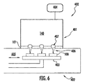
図6は、本開示の第2の実施形態によるプラズマ処理装置のブロック図である。本実施形態において、プラテン403は集束プレート101の下方に配設され、方向605に移動する。重力を使用してワークピース100を支持するとプラテン403が単純化されるが、ワークピースに堆積物または落下粒子が発生する可能性がある。
FIG. 6 is a block diagram of a plasma processing apparatus according to the second embodiment of the present disclosure. In this embodiment, the
図7は、本開示の第3の実施形態によるプラズマ処理装置のブロック図である。本実施形態において、プラテン403は集束プレート101の上方に配設され、方向605に移動する。これによりワークピース100上の堆積物または粒子の形成リスクが解消されるが、プラテン403は、システム400内の処理中にワークピース100を上下逆向きに保持するのに十分なクランプ力を必要とする。
FIG. 7 is a block diagram of a plasma processing apparatus according to the third embodiment of the present disclosure. In this embodiment, the
図8は、本開示の第4の実施形態によるプラズマ処理装置のブロック図である。本実施形態のワークピース100はコンベヤベルト800上に配設され、コンベヤベルト800は垂直方向であってもよい方向405に移動する。
FIG. 8 is a block diagram of a plasma processing apparatus according to the fourth embodiment of the present disclosure. The
図9は、本開示の第5の実施形態によるプラズマ処理装置のブロック図である。ワークピース100はコンベヤベルト800上に配設され、コンベヤベルト800は水平方向であってもよい方向605に移動する。このシステム400は、図6の実施形態の場合と同様に、ワークピース100上に堆積物または粒子が形成される可能性がある。
FIG. 9 is a block diagram of a plasma processing apparatus according to the fifth embodiment of the present disclosure. The
図10は、本開示の第6の実施形態によるプラズマ処理装置のブロック図である。ワークピース100は、方向605に移動するコンベヤベルト800上に配設される。コンベヤベルト405は、ワークピース100が上下逆向きに保持されるようにワークピース100を把持することができる。本実施形態は、ワークピース100上の堆積物または粒子の形成リスクを解消する。
FIG. 10 is a block diagram of a plasma processing apparatus according to the sixth embodiment of the present disclosure.
図5〜図10の各実施形態ではコンベヤベルト800およびプラテン403を図示してあるが、他のワークピース100用搬送機構体を使用してもよい。したがって、本明細書に開示する実施形態は、コンベヤベルト800またはプラテン403だけに限定されるものではない。コンベヤベルト800を使用するいくつかの実施形態は、差動ポンプを使用してプロセスチャンバ402内の真空を維持することができる。
Although the
図11は、本開示の第7の実施形態によるプラズマ処理装置のブロック図である。本実施形態において、少なくともコンベヤベルト800および集束プレート101は傾斜しており、ワークピース100は水平から垂直までの角度であってよい方向1105に移動する。システム400の残りの部分は傾斜させなくてもよいが、図11の実施形態ではシステム400全体が傾斜するように図示してある。コンベヤベルト800を図示してあるが、プラテン403または他のワークピース100用搬送機構体を使用してもよい。傾斜構成を用いるとワークピース100の重力アラインメント(gravity alignment)が可能になるとともに、ワークピース100をコンベヤベルト800上に保持する機構が単純化される。
FIG. 11 is a block diagram of a plasma processing apparatus according to the seventh embodiment of the present disclosure. In this embodiment, at least the
図12は、本開示の第8の実施形態によるプラズマ処理装置のブロック図である。システム1200では、プラズマ源401およびプラズマ源1203を図示してある。プラズマ源1203は、ガス源1202からプラズマ1201を形成する。一例では、プラズマ1201はp型、即ちワークピース100にp型ドーパント種を供給するプラズマであり、プラズマ140はn型、即ちワークピース100にn型ドーパント種を供給するプラズマであるが、プラズマ140およびプラズマ1201がかかる構成に限定されるわけではない。特定の一実施形態では、システム1200を使用して図2に示したIBC太陽電池が形成される。したがって、プラテン403は、プラズマ源401とプラズマ源1203との間でワークピース100を平行移動させて、IBC太陽電池のn型領域とp型領域の両方のドーピングを行う。プラズマ源401、1203は注入期間中にオン・オフを切り替えてもよく、またワークピース100におけるカウンタードーピング効果と連続的に作用させてもよい。バイアスの強さを調整してカウンタードーピング効果を最小限に抑えることも可能である。換言すると、ワークピースのnドーピングすべき部分がプラズマ1201に晒されたとき、およびワークピースのpドーピングすべき部分がプラズマ140に晒されたときに、プラズマとワークピースとの間のバイアスを減少させることができる。
FIG. 12 is a block diagram of a plasma processing apparatus according to the eighth embodiment of the present disclosure. In
プラテン403を図示してあるが、コンベヤベルトまたは他のワークピース100用搬送機構体を使用してもよい。
Although a
図22は、本開示の第9の実施形態によるプラズマ処理装置のブロック図である。システム2200は、プラズマ源401とプラズマ源2201の両方を有する。プラズマ源2201は、ガス源2203からプラズマ2202を形成する。プラテン403を図示してあるが、コンベヤベルトまたは他のワークピース100用搬送機構体を使用してもよい。本実施形態のプラテン403は、プラズマ源401とプラズマ源2201との間で回転または旋回可能である。別の実施形態では、プラテン403または他の何らかの搬送機構体を用いてワークピース100の対向する2つの側面への注入処理を可能にすることができる。別の実施形態では、プラズマ源402とプラズマ源2201が異なる高さに配置されることもある。
FIG. 22 is a block diagram of a plasma processing apparatus according to the ninth embodiment of the present disclosure.
図12および図22の実施形態では、それぞれ2つのプラズマ源を図示してある。3つ以上のプラズマ源を使用してもよい。システム1200および2200を垂直構成として図示したが、本明細書に開示する他の実施形態に類する他の構成も可能である。ブランケット注入と選択的注入、ドーピングと材料改質注入または他の構成のために2つのプラズマ源を使用する他のシステムも可能である。
In the embodiment of FIGS. 12 and 22, two plasma sources are shown respectively. More than two plasma sources may be used. Although
本明細書に開示する諸実施形態では、プラズマ源401のようなプラズマ源を連続動作させてもよい。これによりプラズマ140の生成に要する時間が短縮される。集束プレート101は、システム400内でin‐situ洗浄可能である。一例では、プラズマ源401において洗浄用プラズマを発生させることができる。この予防的メンテナンスは、例えばいくつかの注入サイクルを経た後に実行してもよい。このような洗浄により、堆積物を発生させ得る種がプラズマ源401において使用される場合に、イオン406の所望の特徴または寸法を経時的に維持することが可能となる。集束プレート101の熱制御により集束プレート101上の堆積物を減少させることができる。この熱制御は集束プレートの加熱または冷却を含む可能性がある。
In embodiments disclosed herein, a plasma source, such as
本発明のプラズマ処理装置の諸実施形態は、複数のマスクまたは複雑な注入手法を必要とせずに、選択的な小エリアとブランケット注入の両方を容易にする。これを達成するために、開孔およびワークピース構成は、幅が収束するイオンビームであって、その領域が形成されている開孔と比較して幅がかなり狭い(つまり開孔幅の約75%未満である)領域で基板を捕捉(intercept)するイオンビームを形成する集束イオンの抽出が容易となるように、適切なプラズマパラメータと共に設計することができる。 Embodiments of the plasma processing apparatus of the present invention facilitate both selective small area and blanket implantation without the need for multiple masks or complex implantation techniques. To accomplish this, the aperture and workpiece configuration is an ion beam that converges in width and is much narrower than the aperture in which the region is formed (ie, about 75 of the aperture width). It can be designed with appropriate plasma parameters to facilitate the extraction of focused ions that form an ion beam that intercepts the substrate in the region (below%).
図13は、イオン集束の詳細を示す集束プレートの一実施形態の断面図である。集束プレート101は、開孔407間を距離D1だけ離間させることができる。距離D1は約1cmであってよい。開孔407の長さD2は約2mmであってよい。ワークピース100は、集束プレート101と約1cmの距離D3だけ離間可能である。集束プレート101を使用するワークピース100内の注入領域の幅D4は、約100μmであってよい。集束プレート101は、(図13の紙面に対して垂直方向に)約156mm超の高さを有する開孔407を含むことができる。集束プレート101自体の幅は156mm超であってよい。かかる集束プレート101は、10keV注入用の各開孔407から約0.2A/mのイオン406を抽出することができる。ワークピース100を集束プレート101から約1cm離間させた場合は、ワークピース100におけるイオン406の注入幅を100μmまで絞ることができる。このことは、15個の開孔407が存在するとした場合に、ワークピース100上に468mAのイオン406電流が存在することと等価である。長さD2を約1mmとし、且つプラズマ源を5keVにバイアスし、且つワークピース100を接地した場合は、イオン406を最大10倍以上に集束させることができる。したがって、本発明の諸実施形態は、約10μmの長さD4を有する領域の注入処理に使用可能である。他の集束レベルも可能である。
FIG. 13 is a cross-sectional view of one embodiment of a focusing plate showing details of ion focusing. The focusing
したがって、本発明の諸実施形態は、ミリメートルオーダーの幅の開孔を使用して数ミクロン〜数百ミクロンのオーダーの静止時注入幅(stationary implant width)(つまり、ワークピースを集束イオンに対して走査していないときに得られる注入領域の幅)をもたらすことができる。したがって、静止時注入幅と同じ幅または静止時注入幅より大きい幅(走査を使用する場合)を有する狭い選択的注入領域を形成することが可能となる。さらに、集束イオン406は、幅D2の比較的大きい開孔から抽出されるので、ワークピース100における静止時注入幅D4の全体にわたって高いイオン流束(電流)をもたらす。この結果、ブランケット注入の必要な注入レベルを得るために妥当なワークピース走査レートを実現する十分な高さのイオン電流を提供することにより、より小さいエリアにおける高ドーズ注入に加えて、急速なブランケット注入も容易に実行することが可能となる。
Accordingly, embodiments of the present invention use apertures with a width on the order of millimeters to provide a stationary implant width on the order of a few microns to a few hundred microns (ie, the workpiece relative to the focused ions). The width of the implantation region obtained when not scanning). Accordingly, it is possible to form a narrow selective implantation region having the same width as the stationary implantation width or a width larger than the stationary implantation width (when scanning is used). Further, the
図14は、本発明の方法による注入処理中のステップ移動を示す断面図である。ワークピース100は、イオン406に対して方向405に移動する。これによりワークピース100内に高ドープ領域1400と低ドープ領域1401とが形成される。高ドープ領域1400を形成する際は、低ドープ領域1401の注入処理中に比べてプレート101に対するワークピース100の走査速度を遅くする。かかるプロセスをワークピース100の表面全体に対して繰り返すことができる。
FIG. 14 is a cross-sectional view showing step movement during an implantation process according to the method of the present invention.
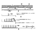
図15A〜図15Dを参照すると、基板100において受け取られるイオンドーズ量1504と、集束プレート101と基板100との間で提供可能な可変走査速度との間の関係が詳細に示されている。静止した基板100に対して集束プレート101を走査することにより、または静止した集束プレート101に対して基板100を走査することにより、または基板と集束プレートの両方を同時に走査することにより、可変走査速度(またはレート)を実現することができる。注入処理中に走査速度を変更することにより、注入レベルが相対的に高い領域と、注入レベルが相対的に低い領域とを形成することが可能となる。図15A〜図15Dに示す実施形態では、可変走査レートを利用して、可変イオンドーズ量1504が基板100に沿ったX方向の位置の関数として示される。図15Aに示すように、集束プレート101を使用してプラズマ140からイオンが抽出され、イオン406が基板100に衝突したときに焦点形状が形成される。イオン406が基板100に注入されたときは、基板100におけるイオンの電流密度1500は、図15Bに示す形をとり得る。図示のとおり、幅1cmの開孔407を通じて抽出されるイオンの電流密度は狭いピークを持ち、イオンが基板100に衝突するときのイオンの幅は約100μmである可能性がある。
Referring to FIGS. 15A-15D, the relationship between the
図15Cは、集束プレート101で使用可能な1つの走査レートシーケンス1502を示す。本実施形態では、走査レートシーケンスを滞留時間関数1504(単位:秒/cm)として示す。この滞留時間関数1504では、滞留時間関数1504のピーク1506が、走査レートが相対的に遅い領域を表し、ベース部分1508が、走査レートが相対的に速い領域を表す。したがって、領域1506では、領域1508と比較して、集束イオン1500が基板100の端から端まで相対的に低速に走査されるので、より高いイオンドーズ量が受け取られることになる。この遅い走査レートと速い走査レートの間の変動が図15Cに示すように周期的に繰り返されるようにすることにより、基板100内のイオンドーズ量1504の周期的な変動をもたらすことが可能となり、したがってX方向にイオンドーピング量が相対的に高い領域と相対的に低い領域とを形成することが可能となる。
FIG. 15C shows one
本発明の諸実施形態は、パルスプラズマ注入を利用してワークピースの様々な領域のドーピングレベルを変更することができる。パルス化DCまたはRF注入の場合、諸代替実施形態では、パルス長またはパルス周波数を増加させて高ドープ領域1400を形成することができる。これらの代替実施形態では、ワークピース100の走査レートを一定に保ちながら、相対的に短いパルスまたは低いパルスレートに晒される領域1401よりもドーピング濃度が高められる領域1400にイオン406が衝突するときに、パルスプラズマのパルスレート(または長さ)を相対的に大きくすることができる。
Embodiments of the present invention can utilize pulsed plasma implantation to change the doping level of various regions of the workpiece. In the case of pulsed DC or RF implantation, in alternate embodiments, the pulse length or pulse frequency can be increased to form the highly doped
本発明の諸実施形態では、図5に開示したような装置を使用して、パルスイオン注入処理に関連する各種パラメータが所望のドーピングレベルに従って変更可能となるように、ワークピースの注入処理を実行することができる。これらのパラメータは、ソースパルスおよび基板パルスのパルス持続時間、パルス周波数および同期化を含むことができる。パルス化の例としては、パルス電位をプラズマに印加すること、またはパルス電位をワークピースに印加することが挙げられる。 In embodiments of the present invention, an apparatus such as that disclosed in FIG. 5 is used to perform the workpiece implantation process such that various parameters associated with the pulsed ion implantation process can be varied according to the desired doping level. can do. These parameters can include the pulse duration, pulse frequency and synchronization of the source and substrate pulses. Examples of pulsing include applying a pulse potential to the plasma or applying a pulse potential to the workpiece.
図18および図19は、それぞれRF同期またはDC同期を使用してワークピースの注入処理を複数の異なるドーパントレベルで実行する本発明の方法に関与する例示的なステップを示す。無論、図18および図19に示したのと異なる方法も可能である。どちらの方法でも周期的な注入パルスを生成しながらターゲット1800を開孔板101等の開孔板に対して走査することができる。図18および図19の各実施形態によれば、注入パルスの「オン」期間中にワークピースとプラズマとの間に電位、例えば負電位を印加し、それによりプラズマ140からの正イオンが集束プレート101を通じて加速され、ワークピース100上に届くようにすることができる。
18 and 19 illustrate exemplary steps involved in the method of the present invention in which the workpiece implantation process is performed at a plurality of different dopant levels using RF synchronization or DC synchronization, respectively. Of course, other methods than those shown in FIGS. 18 and 19 are possible. In either method, the
本発明の特定の実施形態では、既知の技術に従ってプラズマ140をプラズマパルス源によりパルス状に生成することもできる。特に、パルスプラズマは、ワークピース100にバイアスを印加する必要がない構成要素(図示せず)を使用して生成することも可能である。必要に応じて、注入パルスとソースパルスとが全体的に一致するような周期性を有する注入パルスを生成することも可能である。したがって、注入パルスが生成されるときはプラズマ140も「オン」になり、これによりプラズマ140からのイオンが注入パルスによってワークピースに対して加速され、ワークピース100に注入されることになる。基板の異なる領域で異なるドーパントレベルが達成されるようにするために、注入パルスの同期化を異なる形で実施することができる。
In certain embodiments of the present invention, the
特に図18を参照すると、図示の方法は、高ドーズ領域および低ドーズ領域に対応する、ワークピース内の2つの異なるドーピングレベルの領域を形成するのに利用することができる。本方法を使用してターゲット100を開孔板101に対して走査することにより、1つまたは複数のドーピングレベルが相対的に高い領域と、1つまたは複数のドーピングレベルが相対的に低い領域とをターゲット(ワークピース100)内に形成することが可能となる。ステップ1800で、ソースパルスタイミングが生成される。例えば、イオン注入システムに結合されたパルス発生器が100μs毎に50μsの持続時間TONを有するパルスを生成してもよい。
With particular reference to FIG. 18, the illustrated method can be utilized to form two differently doped regions in the workpiece, corresponding to a high dose region and a low dose region. By using the method to scan the
ステップ1802で、所与の領域に高イオンドーズ量を加えるべきかそれとも低イオンドーズ量を加えるべきかが決定される。例えば、集束プレート101の開孔を通って加速されるイオンを使用して低イオンドーズ量領域を形成することが企図される初期ポイントに、ワークピースを集束プレート101に対して配置することができる。したがって、現在のワークピース位置と適用すべき所望の低ドーズ注入とを相関付けるプログラムまたは命令セットをプロセッサによって実行してもよい。
In
ステップ1804および1806で、低イオンドーズ量レベルまたは高イオンドーズ量レベルに応じて、対応するエンコーダパルスがiパルス毎またはjパルス毎に1つ生成される。例えば、低ドーズ(1804)の場合は、エンコーダパルスを200μs毎に相当する2ソースパルス毎に1つ生成し、高ドーズ(1806)の場合は、エンコーダパルスを1000μs毎に相当する20ソースパルス毎に1つ生成するようにしてもよい。
In
一実施形態では、ステップ1808に示すようにモータエンコーダカウントが増分され、且つステップ1810に示すように移動メッセージが走査システムモータに送られるまで、ワークピース100を静止状態に保つことができる。エンコーダパルス間ではワークピースを静止状態としてもよい。したがって、低ドーズの場合のワークピース100への注入処理は、プラズマ140がオンのときの2ソースパルスで構成される。この注入レシピは、ワークピース100への注入処理がワークピース100の移動前の10ソースパルス中に実行される高ドーズの場合と対照的である。したがって、高ドーズ領域が低ドーズ領域の5倍の数の注入パルスに晒されたとすると、高ドーズ領域は低ドーズ領域の5倍のドーズ量を受け取ることになる。
In one embodiment, the
図19に示す方法は図18の方法と同様であるが、同期化を適用してワークピース上の異なる領域につき任意の数の異なるドーピングレベルを達成するのに使用される点が異なる。ステップ1800からステップ1902に進むと、注入処理対象領域に対応する適切なイオン注入ドーズ量が判定される。この判定後、判定した注入対象ドーズ量レベルに対応する代替ステップ(参照符号1904〜1908)のうちの1つに進み、適切なエンコーダパルスシーケンスが生成される。この場合も所望のエリアの注入処理が所望のドーピングレベルに従って達成されるまで、ワークピース100を走査しながらエンコーダパルスシーケンスを印加することができる。図18の場合と同様に、図19の方法は、所望のドーピングレベルに従って、例えば1つ、2つまたは3つのソースパルスが生成されるたびにエンコーダパルスを生成するステップを含む。
The method shown in FIG. 19 is similar to the method of FIG. 18 except that it is used to apply synchronization to achieve any number of different doping levels for different regions on the workpiece. Proceeding from
別の実施形態では、ワークピース100の走査時に、ワークピース100内のドーズ量制御にパルス化RFまたはパルス化DCを使用することができる。このパルス化の時間スケールはマイクロ秒であってよい。例えば、ワークピース100に加えるドーズ量を2%減少させるために、パルス持続時間TONを50μsから49μsに調整してもよい。
In another embodiment, pulsed RF or pulsed DC can be used to control the dose in the
また別の実施形態では、ワークピース100の走査を図14に示す方向405に一定速度で実行する一方、高ドープ領域1400を形成するためにパルス持続時間またはパルスレートを増加させる。例えば、低ドープ領域1401の注入処理と比較して5倍長いパルスまたは5倍高いパルスレートでは、高ドープ領域1400に5倍のドーズ量がもたらされることになる。RFソースパルス化とDCソースパルス化の併用も可能である。かかる併用は、DCパルス中にRFソースのデューティサイクルを修正することによっても、DCパルス中にRFソースの電力レベルを修正することによっても実現可能である。
In yet another embodiment, the
図23および図24は、それぞれパルス化注入システムで適用可能な例示的な電圧曲線2300および2400を時間の関数として示している。上記のとおり、これらの電圧パルスは注入パルスまたはソースパルスを表し得る。図23および図24は、それぞれワークピース位置曲線2310および2410も時間の関数として示している。図23ではワークピースが一定速度で移動しているが、ワークピース内の高ドーズ領域は、パルス2320のようなより長いパルス持続時間によって形成される。ワークピース内の低ドーズ領域は、パルス2330のようなより短いパルス持続時間によって形成される。
FIGS. 23 and 24 show
図24では、ワークピースは線形曲線2410で示されるとおり一定速度で移動する。ワークピース内の高ドーズ領域2420はより高いパルスレートによって形成され、低ドーズ領域2430はより低いパルスレートによって形成される。図23と図24のいずれの実施形態でも、低ドーズ領域を例えば太陽電池のコンタクト間の領域とし、高ドーズ領域を例えば太陽電池のコンタクト下方の領域とすることができる。
In FIG. 24, the workpiece moves at a constant speed as indicated by the
図20A〜図20Cは、ブランケット注入と選択的注入の両方を実行するように構成された集束プレートシステム1210の上面図である。図20Aおよび図20Bに示すように、ワークピース100は方向1204に走査される。集束プレートシステム1210の実施形態は、第1の開孔1202を有する第1の集束プレート1200を含む。第1の開孔1202は、例えば方向1204における走査を行う(ブランケット開孔として機能する)ことにより、ワークピース100の幅全体にわたるブランケット注入を実行し、それにより図20Cに示すようなブランケット領域1220を形成する。第2の集束プレート1201は第2の開孔1203を有する。これら第2の開孔1203は、例えば各開孔1203を同じ方向1204に走査することによりワークピース100のパターン化注入または選択的注入を実行して、パターン化領域1222を形成することができる。この文脈における走査とは、開孔1202および開孔1203に対するワークピース100の相対運動を指し、ワークピース100もしくは集束プレート1200、1201を移動させること、またはワークピース100および集束プレート1200、1201を移動させることにより達成することができる。図20Aおよび図20Bの実施形態では2枚の集束プレートを示しているが、本発明の範囲は、第1の開孔1202と第2の開孔1203を両方有し得る単一の集束プレートもカバーする。図示の例では、集束プレート1200と集束プレート1201が共に、ポイントAからポイントBまでの距離と等しい距離だけ方向1204に沿って走査される。図20Bは、走査完了後の集束プレート1200と集束プレート1201の相対位置を示す。パターン化領域1222は、走査距離を必要に応じて増加させることによりワークピース100の各端縁まで延在させることができる。図20Cは、図20Aに示した初期位置および図20Bに示した最終位置を有する集束プレートの走査を行った後の、ワークピース100の注入ジオメトリの詳細を示す。走査方向1204と直交する方向1212に沿って、第2の開孔1203は第1の開孔1202の一部分と重なるので、第2の開孔1203の下方に露出する注入領域1222はより高いイオンドーズ量を受け取ることになる。
20A-20C are top views of a focusing
本発明によれば、図20Dおよび図20Eに示すように、これらブランケット注入および選択的注入は少なくとも部分的に同時に行ってもよい。図20Dは、開孔1202および開孔1203が同じ集束プレートに含まれる集束プレートシステム1210の一実施形態を示す。図20Dに示すように、集束プレート1210は、方向1204に沿って左に、位置Cまで走査してもよい。図20Dに示す構成は注入走査の途中の一時点を表すものであってもよく、集束プレート1210を引き続きワークピース100に対して左に移動させてもよい。図20Eは、図20Dに示した時点までに集束プレート1210によって形成されたイオン注入のパターンを示す。したがって、位置Cにおけるブランケット集束用開孔1202の前縁に相当する前縁1230aを有するブランケット領域1230が形成されている。走査が進行するとともに、ブランケット領域1230は、図20Cに示した状況と同様にワークピース100全体に延在するようにしてもよい。図20Eは、開孔1203を使用して少なくとも部分的に形成された選択的注入領域1232も示している。さらに、集束プレートでは、例えばドット状、スポット状または他の形状の注入処理を実現する他の開孔構成も可能である。このように、開孔の形状は所望の注入ジオメトリに関連する円形、楕円形または任意の形状とすることができる。
According to the present invention, as shown in FIGS. 20D and 20E, these blanket injection and selective injection may be performed at least partially simultaneously. FIG. 20D shows one embodiment of a focusing
図21は、プロセス制御装置の正面斜視図である。本実施形態において、プロセス制御装置2100はプラテン403およびワークピース100上またはこれらの近傍に配設される。このプロセス制御装置2100は、イオン流束、集束プレートを離れるイオンの寸法または拡散、イオンの場所またはワークピース100に対するイオンの平行度を測定するように構成可能である。第1の開孔2101の長さ寸法は、イオンの長さ寸法よりも大きい。全イオン測定のために、第1の開孔2101の裏側には、磁気抑制または電気抑制可能なファラデーカップ(図示せず)が配設される。第1の開孔2101によって形成される領域を分割して、水平方向のイオン均一性を判定することができる。開孔アレイ2102は互い違いの開孔列を含む。開孔アレイ2102内の各開孔は、想定イオン幅の約1/10である。各開孔アレイ2102の裏側には、磁気抑制または電気抑制可能なファラデーカップ(図示せず)が配設される。水平方向に離間された付加的なアレイセットが、幅または平行度の変化に関する情報を与える。プロセス制御装置2100の領域は、イオンビームが衝突したときにルミネセンスが増加する材料で被覆してもよい。かかるルミネセンスは光学的に監視可能である。第2の開孔2103をプラテン403の周辺に配設して実時間のドーズ量測定を行うこと、および第2の開孔2103を走査速度補正に使用することができる。第2の開孔2103の裏側には、それぞれ分割可能な抑制ファラデーカップ(図示せず)が配設される。
FIG. 21 is a front perspective view of the process control apparatus. In the present embodiment, the
本システムの諸実施形態を使用して二次電子を生成することができる。ワークピース100の帯電は、イオン406内のイオンの軌道に影響を及ぼす可能性がある。二次電子は、集束プレート101の焦点に影響を及ぼす可能性があり、集束プレート101のエッチングを発生させる可能性があり、集束プレート101の加熱を増加させる可能性がある。二次電子は、ワークピース100より低い電位の略透明な電極により抑制することも、ワークピース100の裏側の磁石により抑制することも可能である。図16は、静電抑制の一実施形態を示す断面図である。絶縁体もしくは導体または絶縁層と導電層の組合せであってよい少なくとも1枚の抑制プレート1600が集束プレート101上に配設される。図17Aおよび図17Bは、磁気抑制の2つの実施形態を示す断面図である。磁石1700および磁石1701はそれぞれ逆の極性を有するものであってよく、ワークピース100の裏面(図17A)または集束プレート101とワークピース100との間(図17B)に配設して、二次電子に影響を及ぼすことができる。図17Aにおいて、磁石1700、1701はプラズマ源に対して固定であっても可動であってもよい。図17Bでは、磁石1700、1701を集束プレート101の上部に配設することも、少なくとも部分的に集束プレート101の内部に配設することもできる。図17Bの磁石1700、1701を固定とすることにより動作を単純化することができる。
Embodiments of the system can be used to generate secondary electrons. The charging of the
本明細書に開示の各実施形態は、ワークピース100のドーピングまたはワークピース100の結晶格子の改質に使用可能である。一例では、水素および/またはヘリウム注入を実行してワークピース100の劈開を可能にし、ワークピース100全体に様々なドーズ量の水素および/またはヘリウムを行き渡らせることができる。アモルファス化のような他の材料改質も実行可能である。本明細書に開示の各実施形態を使用した注入処理は、半導体または他の用途に適用可能である。
Each embodiment disclosed herein can be used to dope the
本開示は、本明細書に記載した特定の実施形態によって範囲が限定されるものではない。実際、上記の説明を添付図面と併せて読んだ当業者なら、本明細書に記載したものだけでなく本開示の他の様々な実施形態および修正形態を理解するであろう。したがって、このような他の実施形態および修正形態も本開示の範囲に含まれるものとする。さらに、本明細書では特定の環境、特定の目的および特定の実施形態の文脈で本発明の説明を行ってきたが、本発明の有用性はこれらに限定されるものではなく、本発明は任意の数の環境および任意の数の目的で有利に実施可能であることが当業者には理解されるであろう。したがって、添付の特許請求の範囲の記載は本明細書に記載した本発明の範囲および趣旨に鑑みて解釈すべきものである。 The present disclosure is not to be limited in scope by the specific embodiments described herein. Indeed, those skilled in the art, having read the above description in conjunction with the accompanying drawings, will appreciate various other embodiments and modifications of the present disclosure as well as those described herein. Therefore, such other embodiments and modifications are also included in the scope of the present disclosure. Further, although the present invention has been described herein in the context of a particular environment, a particular purpose, and a particular embodiment, the usefulness of the invention is not limited thereto and the invention is not limited thereto. Those skilled in the art will appreciate that the present invention can be advantageously implemented for any number of environments and for any number of purposes. Accordingly, the description of the appended claims should be construed in view of the scope and spirit of the invention as described herein.
Claims (25)
ワークピースに注入されるイオンを含むプラズマをプラズマチャンバ内に発生させるように構成されたプラズマ源と、
開孔を有する集束プレートであって、該開孔を出たイオンが集束イオンを画定するように該集束プレート近傍のプラズマシースの形状を変更するように構成された集束プレートと、
前記集束イオンの注入幅が前記開孔より実質的に狭くなるように前記集束プレートから離間されたワークピースを収容するプロセスチャンバと
を備え、注入処理中に前記ワークピースを走査することにより前記ワークピース内に複数のパターン化エリアを形成するように構成されることを特徴とする処理装置。 A processing device,
A plasma source configured to generate a plasma in the plasma chamber that includes ions that are implanted into the workpiece;
A focusing plate having an aperture, the focusing plate configured to change a shape of a plasma sheath in the vicinity of the focusing plate such that ions exiting the aperture define the focused ion;
A process chamber containing a workpiece spaced from the focusing plate such that an implantation width of the focused ions is substantially narrower than the aperture, and scanning the workpiece during an implantation process A processing apparatus configured to form a plurality of patterned areas in a piece.
前記処理装置は、
ワークピースホルダと、
第2のプラズマ源と、
開孔を有する第2の集束プレートであって、該開孔は、該開孔を出たイオンが集束イオンを画定するように該第2の集束プレート近傍のプラズマシースの形状を変更するように構成されている、第2の集束プレートと、
前記第2のプラズマ源に結合され、第2の型のイオン種を供給するように構成された第2のプラズマチャンバと
を備え、
前記ワークピースホルダは、前記第1の型のイオン種および前記第2の型のイオン種にそれぞれ対応する第1の領域および第2の領域が前記ワークピースに選択的に注入されるように、前記集束プレートおよび前記第2の集束プレートの下方を走査するように構成される請求項1に記載の処理装置。 The ions in the plasma chamber are a first type of ionic species;
The processor is
A workpiece holder;
A second plasma source;
A second focusing plate having an aperture, the aperture changing the shape of the plasma sheath near the second focusing plate such that ions exiting the aperture define the focused ion A second focusing plate configured;
A second plasma chamber coupled to the second plasma source and configured to supply a second type of ionic species;
The workpiece holder is selectively implanted into the workpiece with a first region and a second region corresponding to the first type ion species and the second type ion species, respectively. The processing apparatus of claim 1, configured to scan below the focusing plate and the second focusing plate.
プラズマを収容したプラズマチャンバに隣接して、前記ワークピースに向かって集束イオンを提供する少なくとも1つの開孔を通じて前記プラズマからイオンを抽出するように構成された集束プレートを設けるステップと、
ワークピースホルダと前記プラズマとの間にバイアスをかけて、前記集束イオンが前記ワークピースホルダ上に配設された前記ワークピースに引き寄せられるようにするステップと、
前記ワークピースを前記集束プレートに対して走査して、複数の選択的注入エリアが形成されるようにするステップと
を含むことを特徴とする方法。 A method of performing a workpiece injection process,
Providing a focusing plate adjacent to a plasma chamber containing plasma and configured to extract ions from the plasma through at least one aperture that provides focused ions toward the workpiece;
Biasing between a workpiece holder and the plasma so that the focused ions are attracted to the workpiece disposed on the workpiece holder;
Scanning the workpiece with respect to the focusing plate to form a plurality of selective injection areas.
前記集束プレートの開孔が前記ワークピースの第1の領域を覆う位置に配置されたときに、第1のバイアスパルス周波数を有し前記ソースパルスと同期された第1のバイアスパルスセットを提供するステップと、
前記集束プレートの前記開孔が前記ワークピースの第2の領域を覆う位置に配置されたときに、前記第1のバイアスパルス周波数と異なる第2のバイアスパルス周波数を有し、前記ソースパルスと同期された第2のバイアスパルスセットを提供するステップと
をさらに含む請求項17に記載の方法。 Supplying a source pulse having a first pulse frequency to the plasma;
Providing a first bias pulse set having a first bias pulse frequency and synchronized with the source pulse when the aperture of the focusing plate is positioned to cover the first region of the workpiece. Steps,
Having a second bias pulse frequency different from the first bias pulse frequency and synchronized with the source pulse when the aperture of the focusing plate is disposed at a position covering the second region of the workpiece. And providing a second set of bias pulses.
n型ドーパントイオンを有する第1のプラズマを収容した第1のプラズマチャンバに隣接して、前記ワークピースに向かって集束イオンを提供する少なくとも1つの開孔を通じて前記プラズマからイオンを抽出するように構成された第1の集束プレートを設けるステップと、
p型ドーパントイオンを有する第2のプラズマを収容した第2のプラズマチャンバに隣接して、前記ワークピースに向かって集束イオンを提供する少なくとも1つの開孔を通じて前記プラズマからイオンを抽出するように構成された第2の集束プレートを設けるステップと、
前記ワークピースと前記第1のプラズマおよび第2のプラズマとの間にそれぞれバイアスを印加しながら、前記ワークピースを前記第1の集束プレートおよび前記第2の集束プレートに対して走査するステップと
を含み、選択的にnドーピングされる1組のエリアと、選択的にpドーピングされる別の1組のエリアとが、前記ワークピース内に形成されることを特徴とする方法。 A method of performing workpiece injection processing in a plasma processing system,
Constructed to extract ions from the plasma through at least one aperture that provides focused ions toward the workpiece adjacent to a first plasma chamber containing a first plasma having n-type dopant ions. Providing a first focusing plate formed;
Constructed to extract ions from the plasma through at least one aperture that provides focused ions towards the workpiece adjacent to a second plasma chamber containing a second plasma having p-type dopant ions. Providing a second focusing plate formed;
Scanning the workpiece relative to the first focusing plate and the second focusing plate while applying a bias between the workpiece and the first plasma and the second plasma, respectively. A method wherein a set of selectively n-doped areas and another set of selectively p-doped areas are formed in the workpiece.
Applications Claiming Priority (5)
| Application Number | Priority Date | Filing Date | Title |
|---|---|---|---|
| US26198309P | 2009-11-17 | 2009-11-17 | |
| US61/261,983 | 2009-11-17 | ||
| US12/947,078 | 2010-11-16 | ||
| US12/947,078 US8461030B2 (en) | 2009-11-17 | 2010-11-16 | Apparatus and method for controllably implanting workpieces |
| PCT/US2010/056952 WO2011062945A1 (en) | 2009-11-17 | 2010-11-17 | Apparatus and method for controllably implanting workpieces |
Publications (2)
| Publication Number | Publication Date |
|---|---|
| JP2013511823A true JP2013511823A (en) | 2013-04-04 |
| JP2013511823A5 JP2013511823A5 (en) | 2013-11-21 |
Family
ID=43601664
Family Applications (1)
| Application Number | Title | Priority Date | Filing Date |
|---|---|---|---|
| JP2012539080A Pending JP2013511823A (en) | 2009-11-17 | 2010-11-17 | Apparatus and method for controllably performing workpiece injection process |
Country Status (7)
| Country | Link |
|---|---|
| US (2) | US8461030B2 (en) |
| EP (1) | EP2502254A1 (en) |
| JP (1) | JP2013511823A (en) |
| KR (1) | KR20120105469A (en) |
| CN (1) | CN102971825A (en) |
| TW (1) | TWI485743B (en) |
| WO (1) | WO2011062945A1 (en) |
Cited By (3)
| Publication number | Priority date | Publication date | Assignee | Title |
|---|---|---|---|---|
| JP2017533542A (en) * | 2014-09-10 | 2017-11-09 | ヴァリアン セミコンダクター イクイップメント アソシエイツ インコーポレイテッド | Control of ion angle distribution of ion beam using hidden deflection electrode |
| JP2018504774A (en) * | 2014-12-18 | 2018-02-15 | ヴァリアン セミコンダクター イクイップメント アソシエイツ インコーポレイテッド | Dynamic heating method and system for wafer processing |
| JP2020521322A (en) * | 2017-05-19 | 2020-07-16 | トタル ソシエテ アノニムTotal Sa | Apparatus and method for pattern structure processing |
Families Citing this family (25)
| Publication number | Priority date | Publication date | Assignee | Title |
|---|---|---|---|---|
| US20110027463A1 (en) * | 2009-06-16 | 2011-02-03 | Varian Semiconductor Equipment Associates, Inc. | Workpiece handling system |
| US8749053B2 (en) | 2009-06-23 | 2014-06-10 | Intevac, Inc. | Plasma grid implant system for use in solar cell fabrications |
| US8164068B2 (en) * | 2009-07-30 | 2012-04-24 | Varian Semiconductor Equipment Associates, Inc. | Mask health monitor using a faraday probe |
| US8592230B2 (en) | 2010-04-22 | 2013-11-26 | Varian Semiconductor Equipment Associates, Inc. | Method for patterning a substrate using ion assisted selective depostion |
| US8435727B2 (en) | 2010-10-01 | 2013-05-07 | Varian Semiconductor Equipment Associates, Inc. | Method and system for modifying photoresist using electromagnetic radiation and ion implantation |
| KR101915753B1 (en) * | 2010-10-21 | 2018-11-07 | 삼성디스플레이 주식회사 | Ion implantation system and method for implanting ions using the same |
| DE102010060910A1 (en) * | 2010-11-30 | 2012-05-31 | Roth & Rau Ag | Method and apparatus for ion implantation |
| US8907307B2 (en) * | 2011-03-11 | 2014-12-09 | Varian Semiconductor Equipment Associates, Inc. | Apparatus and method for maskless patterned implantation |
| US8716682B2 (en) * | 2011-04-04 | 2014-05-06 | Varian Semiconductor Equipment Associates, Inc. | Apparatus and method for multiple slot ion implantation |
| US8288741B1 (en) * | 2011-08-16 | 2012-10-16 | Varian Semiconductor Equipment Associates, Inc. | Apparatus and method for three dimensional ion processing |
| US9437392B2 (en) | 2011-11-02 | 2016-09-06 | Varian Semiconductor Equipment Associates, Inc. | High-throughput ion implanter |
| CN106847736B (en) | 2011-11-08 | 2020-08-11 | 因特瓦克公司 | Substrate processing system and method |
| US9297063B2 (en) | 2012-04-26 | 2016-03-29 | Varian Semiconductor Equipment Associates, Inc. | Plasma potential modulated ion implantation system |
| JP2014045036A (en) * | 2012-08-24 | 2014-03-13 | Amaya Corp | Semiconductor device manufacturing method |
| TWI570745B (en) | 2012-12-19 | 2017-02-11 | 因特瓦克公司 | Grid for plasma ion implant |
| US9232628B2 (en) | 2013-02-20 | 2016-01-05 | Varian Semiconductor Equipment Associates, Inc. | Method and system for plasma-assisted ion beam processing |
| US9236257B2 (en) * | 2013-03-13 | 2016-01-12 | Varian Semiconductor Equipment Associates, Inc. | Techniques to mitigate straggle damage to sensitive structures |
| US20140360670A1 (en) * | 2013-06-05 | 2014-12-11 | Tokyo Electron Limited | Processing system for non-ambipolar electron plasma (nep) treatment of a substrate with sheath potential |
| JP6150632B2 (en) * | 2013-06-26 | 2017-06-21 | 住友重機械イオンテクノロジー株式会社 | Ion beam measuring apparatus and ion beam measuring method |
| US9711316B2 (en) | 2013-10-10 | 2017-07-18 | Varian Semiconductor Equipment Associates, Inc. | Method of cleaning an extraction electrode assembly using pulsed biasing |
| US9520267B2 (en) * | 2014-06-20 | 2016-12-13 | Applied Mateirals, Inc. | Bias voltage frequency controlled angular ion distribution in plasma processing |
| US10730082B2 (en) * | 2016-10-26 | 2020-08-04 | Varian Semiconductor Equipment Associates, Inc. | Apparatus and method for differential in situ cleaning |
| US10276340B1 (en) * | 2017-12-20 | 2019-04-30 | Varian Semiconductor Equipment Associates, Inc. | Low particle capacitively coupled components for workpiece processing |
| US10468226B1 (en) | 2018-09-21 | 2019-11-05 | Varian Semiconductor Equipment Associates, Inc. | Extraction apparatus and system for high throughput ion beam processing |
| US11193198B2 (en) * | 2018-12-17 | 2021-12-07 | Applied Materials, Inc. | Methods of forming devices on a substrate |
Citations (8)
| Publication number | Priority date | Publication date | Assignee | Title |
|---|---|---|---|---|
| JPS4979457A (en) * | 1972-12-04 | 1974-07-31 | ||
| JPS58180227A (en) * | 1982-04-17 | 1983-10-21 | Samuko Internatl Kenkyusho:Kk | Efficient plasma treating apparatus having plural reaction chambers |
| JPH03255622A (en) * | 1990-03-05 | 1991-11-14 | Matsushita Electric Ind Co Ltd | Method and apparatus for doping semiconductor |
| JPH08213339A (en) * | 1995-02-02 | 1996-08-20 | Hitachi Ltd | Ion implantation and device thereof |
| JP2000012285A (en) * | 1998-06-26 | 2000-01-14 | Nissin Electric Co Ltd | Pulse bias hydrogen negative ion implantation method and implantation device |
| US20050051517A1 (en) * | 2003-08-12 | 2005-03-10 | Oehrlein Gottlieb S. | Method and system for nanoscale plasma processing of objects |
| JP2006196752A (en) * | 2005-01-14 | 2006-07-27 | Ulvac Japan Ltd | System and method for doping plasma |
| WO2009033134A2 (en) * | 2007-09-07 | 2009-03-12 | Varian Semiconductor Equipment Associates, Inc. | A patterned assembly for manufacturing a solar cell and a method thereof |
Family Cites Families (20)
| Publication number | Priority date | Publication date | Assignee | Title |
|---|---|---|---|---|
| US4074139A (en) | 1976-12-27 | 1978-02-14 | Rca Corporation | Apparatus and method for maskless ion implantation |
| DE2835136A1 (en) | 1978-08-10 | 1980-02-14 | Fraunhofer Ges Forschung | Semiconductor solar cell - with pattern of higher dopant concentration on substrate doped by ion implantation |
| JP4204662B2 (en) | 1998-04-02 | 2009-01-07 | 株式会社アルバック | Ion implantation apparatus and ion implantation method |
| US6203862B1 (en) | 1998-05-13 | 2001-03-20 | Intevac, Inc. | Processing systems with dual ion sources |
| JP2001189483A (en) | 1999-10-18 | 2001-07-10 | Sharp Corp | Solar battery cell with bypass function, multi-junction laminating type solar battery cell with bypass function, and their manufacturing method |
| US6534775B1 (en) | 2000-09-01 | 2003-03-18 | Axcelis Technologies, Inc. | Electrostatic trap for particles entrained in an ion beam |
| DE102004063691B4 (en) * | 2004-05-10 | 2019-01-17 | Hynix Semiconductor Inc. | Method for implanting ions in a semiconductor device |
| JP2006278006A (en) | 2005-03-28 | 2006-10-12 | Japan Atomic Energy Agency | Plasma boundary surface control method in ion source extraction region and its ion source |
| US7524743B2 (en) | 2005-10-13 | 2009-04-28 | Varian Semiconductor Equipment Associates, Inc. | Conformal doping apparatus and method |
| US20090142875A1 (en) | 2007-11-30 | 2009-06-04 | Applied Materials, Inc. | Method of making an improved selective emitter for silicon solar cells |
| US7727866B2 (en) | 2008-03-05 | 2010-06-01 | Varian Semiconductor Equipment Associates, Inc. | Use of chained implants in solar cells |
| US20090317937A1 (en) | 2008-06-20 | 2009-12-24 | Atul Gupta | Maskless Doping Technique for Solar Cells |
| JP2011524640A (en) | 2008-06-11 | 2011-09-01 | インテバック・インコーポレイテッド | Solar cell forming method and solar cell |
| US8356550B2 (en) | 2008-07-25 | 2013-01-22 | Federal-Mogul Corporation | Piston skirt with friction reducing oil recess and oil reservoir |
| US8101510B2 (en) * | 2009-04-03 | 2012-01-24 | Varian Semiconductor Equipment Associates, Inc. | Plasma processing apparatus |
| US7767977B1 (en) | 2009-04-03 | 2010-08-03 | Varian Semiconductor Equipment Associates, Inc. | Ion source |
| US8623171B2 (en) | 2009-04-03 | 2014-01-07 | Varian Semiconductor Equipment Associates, Inc. | Plasma processing apparatus |
| US8749053B2 (en) | 2009-06-23 | 2014-06-10 | Intevac, Inc. | Plasma grid implant system for use in solar cell fabrications |
| US8008176B2 (en) | 2009-08-11 | 2011-08-30 | Varian Semiconductor Equipment Associates, Inc. | Masked ion implant with fast-slow scan |
| US8173527B2 (en) | 2009-10-19 | 2012-05-08 | Varian Semiconductor Equipment Associates, Inc. | Stepped masking for patterned implantation |
-
2010
- 2010-11-16 US US12/947,078 patent/US8461030B2/en active Active
- 2010-11-17 EP EP10788436A patent/EP2502254A1/en not_active Withdrawn
- 2010-11-17 WO PCT/US2010/056952 patent/WO2011062945A1/en active Application Filing
- 2010-11-17 TW TW099139576A patent/TWI485743B/en not_active IP Right Cessation
- 2010-11-17 CN CN2010800515328A patent/CN102971825A/en active Pending
- 2010-11-17 JP JP2012539080A patent/JP2013511823A/en active Pending
- 2010-11-17 KR KR1020127015077A patent/KR20120105469A/en not_active Application Discontinuation
-
2013
- 2013-04-19 US US13/866,315 patent/US8937004B2/en not_active Expired - Fee Related
Patent Citations (9)
| Publication number | Priority date | Publication date | Assignee | Title |
|---|---|---|---|---|
| JPS4979457A (en) * | 1972-12-04 | 1974-07-31 | ||
| JPS58180227A (en) * | 1982-04-17 | 1983-10-21 | Samuko Internatl Kenkyusho:Kk | Efficient plasma treating apparatus having plural reaction chambers |
| JPH03255622A (en) * | 1990-03-05 | 1991-11-14 | Matsushita Electric Ind Co Ltd | Method and apparatus for doping semiconductor |
| JPH08213339A (en) * | 1995-02-02 | 1996-08-20 | Hitachi Ltd | Ion implantation and device thereof |
| JP2000012285A (en) * | 1998-06-26 | 2000-01-14 | Nissin Electric Co Ltd | Pulse bias hydrogen negative ion implantation method and implantation device |
| US20050051517A1 (en) * | 2003-08-12 | 2005-03-10 | Oehrlein Gottlieb S. | Method and system for nanoscale plasma processing of objects |
| JP2006196752A (en) * | 2005-01-14 | 2006-07-27 | Ulvac Japan Ltd | System and method for doping plasma |
| WO2009033134A2 (en) * | 2007-09-07 | 2009-03-12 | Varian Semiconductor Equipment Associates, Inc. | A patterned assembly for manufacturing a solar cell and a method thereof |
| JP2010539684A (en) * | 2007-09-07 | 2010-12-16 | ヴァリアン セミコンダクター イクイップメント アソシエイツ インコーポレイテッド | Patterned assembly for solar cell manufacturing and method for manufacturing solar cell |
Non-Patent Citations (1)
| Title |
|---|
| JPN5013000263; KWOK D.T.K.: 'ONE-STEP, NON-CONTACT PATTERN TRANSFER BY DIRECT-CURRENT PLASMA IMMERSION ION IMPLANTATION' JOURNAL OF PHYSICS D: APPLIED PHYSICS V42 N19, 20091007, IOP PUBLISHING LTD * |
Cited By (4)
| Publication number | Priority date | Publication date | Assignee | Title |
|---|---|---|---|---|
| JP2017533542A (en) * | 2014-09-10 | 2017-11-09 | ヴァリアン セミコンダクター イクイップメント アソシエイツ インコーポレイテッド | Control of ion angle distribution of ion beam using hidden deflection electrode |
| JP2018504774A (en) * | 2014-12-18 | 2018-02-15 | ヴァリアン セミコンダクター イクイップメント アソシエイツ インコーポレイテッド | Dynamic heating method and system for wafer processing |
| JP2020521322A (en) * | 2017-05-19 | 2020-07-16 | トタル ソシエテ アノニムTotal Sa | Apparatus and method for pattern structure processing |
| JP7335815B2 (en) | 2017-05-19 | 2023-08-30 | トタルエネルジ エスウ | Apparatus and method for patterned structure processing |
Also Published As
| Publication number | Publication date |
|---|---|
| TWI485743B (en) | 2015-05-21 |
| US8461030B2 (en) | 2013-06-11 |
| US8937004B2 (en) | 2015-01-20 |
| EP2502254A1 (en) | 2012-09-26 |
| CN102971825A (en) | 2013-03-13 |
| KR20120105469A (en) | 2012-09-25 |
| TW201142906A (en) | 2011-12-01 |
| US20130234034A1 (en) | 2013-09-12 |
| WO2011062945A1 (en) | 2011-05-26 |
| US20110124186A1 (en) | 2011-05-26 |
Similar Documents
| Publication | Publication Date | Title |
|---|---|---|
| US8937004B2 (en) | Apparatus and method for controllably implanting workpieces | |
| KR101409925B1 (en) | Method of manufacturing solar cell using substrate | |
| TWI600062B (en) | Ion implantation method, apparatus using the same, and article executing the same | |
| US8716682B2 (en) | Apparatus and method for multiple slot ion implantation | |
| US8187979B2 (en) | Workpiece patterning with plasma sheath modulation | |
| US20090227095A1 (en) | Counterdoping for solar cells | |
| US9863032B2 (en) | Techniques for processing a substrate | |
| US9006688B2 (en) | Techniques for processing a substrate using a mask | |
| CN107039251B (en) | DC ion implantation for solid phase epitaxial regrowth in solar cell fabrication | |
| US20110089343A1 (en) | Techniques for processing a substrate | |
| WO2012003154A1 (en) | Deceleration lens | |
| US8183546B2 (en) | Ion implantation through laser fields |
Legal Events
| Date | Code | Title | Description |
|---|---|---|---|
| A521 | Written amendment |
Free format text: JAPANESE INTERMEDIATE CODE: A523 Effective date: 20130214 |
|
| A521 | Written amendment |
Free format text: JAPANESE INTERMEDIATE CODE: A821 Effective date: 20130214 |
|
| A521 | Written amendment |
Free format text: JAPANESE INTERMEDIATE CODE: A523 Effective date: 20131001 |
|
| A621 | Written request for application examination |
Free format text: JAPANESE INTERMEDIATE CODE: A621 Effective date: 20131001 |
|
| A977 | Report on retrieval |
Free format text: JAPANESE INTERMEDIATE CODE: A971007 Effective date: 20140829 |
|
| A131 | Notification of reasons for refusal |
Free format text: JAPANESE INTERMEDIATE CODE: A131 Effective date: 20141007 |
|
| A02 | Decision of refusal |
Free format text: JAPANESE INTERMEDIATE CODE: A02 Effective date: 20150804 |