KR20120097765A - Touch sensor integrated display device - Google Patents
Touch sensor integrated display device Download PDFInfo
- Publication number
- KR20120097765A KR20120097765A KR1020110017181A KR20110017181A KR20120097765A KR 20120097765 A KR20120097765 A KR 20120097765A KR 1020110017181 A KR1020110017181 A KR 1020110017181A KR 20110017181 A KR20110017181 A KR 20110017181A KR 20120097765 A KR20120097765 A KR 20120097765A
- Authority
- KR
- South Korea
- Prior art keywords
- touch
- line
- gate
- electrode
- electrodes
- Prior art date
Links
Images


Classifications
-
- G—PHYSICS
- G02—OPTICS
- G02F—OPTICAL DEVICES OR ARRANGEMENTS FOR THE CONTROL OF LIGHT BY MODIFICATION OF THE OPTICAL PROPERTIES OF THE MEDIA OF THE ELEMENTS INVOLVED THEREIN; NON-LINEAR OPTICS; FREQUENCY-CHANGING OF LIGHT; OPTICAL LOGIC ELEMENTS; OPTICAL ANALOGUE/DIGITAL CONVERTERS
- G02F1/00—Devices or arrangements for the control of the intensity, colour, phase, polarisation or direction of light arriving from an independent light source, e.g. switching, gating or modulating; Non-linear optics
- G02F1/01—Devices or arrangements for the control of the intensity, colour, phase, polarisation or direction of light arriving from an independent light source, e.g. switching, gating or modulating; Non-linear optics for the control of the intensity, phase, polarisation or colour
- G02F1/13—Devices or arrangements for the control of the intensity, colour, phase, polarisation or direction of light arriving from an independent light source, e.g. switching, gating or modulating; Non-linear optics for the control of the intensity, phase, polarisation or colour based on liquid crystals, e.g. single liquid crystal display cells
- G02F1/133—Constructional arrangements; Operation of liquid crystal cells; Circuit arrangements
- G02F1/1333—Constructional arrangements; Manufacturing methods
- G02F1/1343—Electrodes
- G02F1/134309—Electrodes characterised by their geometrical arrangement
-
- G—PHYSICS
- G02—OPTICS
- G02F—OPTICAL DEVICES OR ARRANGEMENTS FOR THE CONTROL OF LIGHT BY MODIFICATION OF THE OPTICAL PROPERTIES OF THE MEDIA OF THE ELEMENTS INVOLVED THEREIN; NON-LINEAR OPTICS; FREQUENCY-CHANGING OF LIGHT; OPTICAL LOGIC ELEMENTS; OPTICAL ANALOGUE/DIGITAL CONVERTERS
- G02F1/00—Devices or arrangements for the control of the intensity, colour, phase, polarisation or direction of light arriving from an independent light source, e.g. switching, gating or modulating; Non-linear optics
- G02F1/01—Devices or arrangements for the control of the intensity, colour, phase, polarisation or direction of light arriving from an independent light source, e.g. switching, gating or modulating; Non-linear optics for the control of the intensity, phase, polarisation or colour
- G02F1/13—Devices or arrangements for the control of the intensity, colour, phase, polarisation or direction of light arriving from an independent light source, e.g. switching, gating or modulating; Non-linear optics for the control of the intensity, phase, polarisation or colour based on liquid crystals, e.g. single liquid crystal display cells
- G02F1/133—Constructional arrangements; Operation of liquid crystal cells; Circuit arrangements
- G02F1/13306—Circuit arrangements or driving methods for the control of single liquid crystal cells
-
- G—PHYSICS
- G02—OPTICS
- G02F—OPTICAL DEVICES OR ARRANGEMENTS FOR THE CONTROL OF LIGHT BY MODIFICATION OF THE OPTICAL PROPERTIES OF THE MEDIA OF THE ELEMENTS INVOLVED THEREIN; NON-LINEAR OPTICS; FREQUENCY-CHANGING OF LIGHT; OPTICAL LOGIC ELEMENTS; OPTICAL ANALOGUE/DIGITAL CONVERTERS
- G02F1/00—Devices or arrangements for the control of the intensity, colour, phase, polarisation or direction of light arriving from an independent light source, e.g. switching, gating or modulating; Non-linear optics
- G02F1/01—Devices or arrangements for the control of the intensity, colour, phase, polarisation or direction of light arriving from an independent light source, e.g. switching, gating or modulating; Non-linear optics for the control of the intensity, phase, polarisation or colour
- G02F1/13—Devices or arrangements for the control of the intensity, colour, phase, polarisation or direction of light arriving from an independent light source, e.g. switching, gating or modulating; Non-linear optics for the control of the intensity, phase, polarisation or colour based on liquid crystals, e.g. single liquid crystal display cells
- G02F1/133—Constructional arrangements; Operation of liquid crystal cells; Circuit arrangements
- G02F1/1333—Constructional arrangements; Manufacturing methods
- G02F1/13338—Input devices, e.g. touch panels
-
- G—PHYSICS
- G02—OPTICS
- G02F—OPTICAL DEVICES OR ARRANGEMENTS FOR THE CONTROL OF LIGHT BY MODIFICATION OF THE OPTICAL PROPERTIES OF THE MEDIA OF THE ELEMENTS INVOLVED THEREIN; NON-LINEAR OPTICS; FREQUENCY-CHANGING OF LIGHT; OPTICAL LOGIC ELEMENTS; OPTICAL ANALOGUE/DIGITAL CONVERTERS
- G02F1/00—Devices or arrangements for the control of the intensity, colour, phase, polarisation or direction of light arriving from an independent light source, e.g. switching, gating or modulating; Non-linear optics
- G02F1/01—Devices or arrangements for the control of the intensity, colour, phase, polarisation or direction of light arriving from an independent light source, e.g. switching, gating or modulating; Non-linear optics for the control of the intensity, phase, polarisation or colour
- G02F1/13—Devices or arrangements for the control of the intensity, colour, phase, polarisation or direction of light arriving from an independent light source, e.g. switching, gating or modulating; Non-linear optics for the control of the intensity, phase, polarisation or colour based on liquid crystals, e.g. single liquid crystal display cells
- G02F1/133—Constructional arrangements; Operation of liquid crystal cells; Circuit arrangements
- G02F1/1333—Constructional arrangements; Manufacturing methods
- G02F1/1343—Electrodes
- G02F1/134309—Electrodes characterised by their geometrical arrangement
- G02F1/134318—Electrodes characterised by their geometrical arrangement having a patterned common electrode
-
- G—PHYSICS
- G06—COMPUTING; CALCULATING OR COUNTING
- G06F—ELECTRIC DIGITAL DATA PROCESSING
- G06F3/00—Input arrangements for transferring data to be processed into a form capable of being handled by the computer; Output arrangements for transferring data from processing unit to output unit, e.g. interface arrangements
- G06F3/01—Input arrangements or combined input and output arrangements for interaction between user and computer
- G06F3/03—Arrangements for converting the position or the displacement of a member into a coded form
- G06F3/041—Digitisers, e.g. for touch screens or touch pads, characterised by the transducing means
- G06F3/0412—Digitisers structurally integrated in a display
-
- G—PHYSICS
- G06—COMPUTING; CALCULATING OR COUNTING
- G06F—ELECTRIC DIGITAL DATA PROCESSING
- G06F2203/00—Indexing scheme relating to G06F3/00 - G06F3/048
- G06F2203/041—Indexing scheme relating to G06F3/041 - G06F3/045
- G06F2203/04103—Manufacturing, i.e. details related to manufacturing processes specially suited for touch sensitive devices
Abstract
Description
본 발명은 표시장치에 관한 것으로, 특히 터치 센서 일체형 표시장치에 관한 것이다.
The present invention relates to a display device, and more particularly to a display device with a touch sensor.
터치 센서는 액정 표시장치(Liquid Crystal Display), 전계 방출 표시장치(Field Emission Display, FED), 플라즈마 디스플레이 패널(Plasma Display Panel, PDP), 전계발광 표시장치(Electroluminescence Device, EL), 전기영동 표시장치 등과 같은 화상표시장치에 설치되어 사용자가 화상표시장치를 보면서 터치 패널을 가압하여(누르거나 터치하여) 미리 정해진 정보를 입력하는 입력장치의 한 종류이다.Touch sensors include Liquid Crystal Display, Field Emission Display (FED), Plasma Display Panel (PDP), Electroluminescence Device (EL), Electrophoretic Display It is a type of input device installed in an image display device such as an input device for inputting predetermined information by pressing (touching or touching) the touch panel while the user views the image display device.
상술한 표시장치에 사용되는 터치 센서는 그 구조에 따라 상판 부착형(add-on type), 상판 일체형(on-cell type) 및 내장형(integrated type)으로 나눌 수 있다. 상판 부착형은 표시장치와 터치 센서를 개별적으로 제조한 후에, 표시장치의 상판에 터치 센서를 부착하는 방식이다. 상판 일체형은 표시장치의 상부 유리 기판 표면에 터치 세서를 구성하는 소자들을 직접 형성하는 방식이다. 내장형은 표시장치 내부에 터치 센서를 내장하여 표시장치의 박형화를 달성하고 내구성을 높일 수 있는 방식이다.The touch sensor used in the above-described display device may be classified into an add-on type, an on-cell type, and an integrated type according to its structure. The top plate attaching type is a method of attaching the touch sensor to the top plate of the display device after separately manufacturing the display device and the touch sensor. The upper plate integrated type directly forms elements constituting the touch parser on the upper glass substrate surface of the display device. The built-in type has a built-in touch sensor inside the display device to achieve a thin display device and enhance durability.
그러나, 상판 부착형 터치 센서는 표시장치 위에 완성된 터치 센서가 올라가 장착되는 구조로 두께가 두껍고, 표시장치의 밝기가 어두워져 시인성이 저하되는 문제가 있다. 또한, 상판 일체형 터치 센서는 표시장치의 상면에 별도의 터치 센서가 형성된 구조로서, 상판 부착형 보다 두께를 줄일 수 있지만, 여전히 터치 센서를 구성하는 구동전극층과 센싱전극층 및 이들을 절연시키기 위한 절연층 때문에 전체 두께가 증가하고 공정수가 증가하여 제조가격이 증가하는 문제점이 있었다. However, the top-mounted touch sensor has a structure in which the completed touch sensor is mounted on the display device and is thick, and the brightness of the display device is dark. In addition, the upper panel integrated touch sensor has a structure in which a separate touch sensor is formed on the upper surface of the display device, and may have a thickness smaller than that of the upper panel attached type, but is still due to the driving electrode layer, the sensing electrode layer, and the insulating layer for insulating the touch sensor. There was a problem that the manufacturing thickness increases due to the increase in the overall thickness and the number of processes.
한편, 내장형 터치 센서는 내구성 향상과 박형화가 가능하다는 점에서 상판 부착형과 상판 일체형의 터치 센서에 의해 발생하는 문제점들을 해결할 수 있는 장점이 있다. 이러한 내장형 터치 센서는 광 방식, 정전용량 방식 등이 있다.On the other hand, the built-in touch sensor has the advantage that can solve the problems caused by the top plate attached and the top plate integrated touch sensor in that durability and thickness can be reduced. Such a built-in touch sensor may be an optical method, a capacitive method.
광방식 터치 센서는 표시장치의 박막 트랜지스터 기판 어레이에 광센싱층을 형성하고, 백라이트 유닛으로부터의 광이나 적외선 광을 이용하여 터치된 부분에 존재하는 물체를 통해 반사된 광을 인식하는 방식이다. 그러나, 광 방식 터치 센서는 주변이 어두운 경우 비교적 안정된 구동성능을 보여주지만, 주변이 밝은 경우 반사된 광보다 더 강한 광들이 노이즈로 작용하게 된다. 실제 터치에 의해 반사되는 광의 세기는 매우 약하여 외부가 조금만 밝아도 터치인식에 오류가 발생할 수 있기 때문이다. 특히, 광 방식 터치 센서는 주변환경이 태양광에 노출되는 경우 광의 세기가 워낙 강하여 아에 터치 인식이 되는 않은 경우도 발생할 수 있는 문제점이 있다.The optical touch sensor is a method of forming a light sensing layer on a thin film transistor substrate array of a display device and recognizing light reflected through an object present in a touched portion by using light from an backlight unit or infrared light. However, the optical touch sensor shows relatively stable driving performance when the surroundings are dark, but light stronger than the reflected light acts as noise when the surroundings are bright. This is because the intensity of light reflected by the actual touch is so weak that even a little bright outside may cause an error in touch recognition. In particular, the optical touch sensor has a problem that may occur even when the surrounding environment is exposed to sunlight, the light intensity is so strong that the touch is not recognized in the child.
정전용량 방식 터치센서는 자기 정전용량방식(self capacitance Type)과 상호정전용량 방식(mutual capacitance type)이 있다. 상호 정전용량방식 터치 센서는 디스플레이용 공통전극을 분할하고, 이를 구동전극 영역과 센싱전극 영역으로 나누어 구동전극 영역과 센싱전극 영역 사이에 상호 정전용량(mutual capacitance)이 형성되도록 함으로써 터치시 발생하는 상호 정전용량의 변화량을 측정하여 터치를 인식하는 방법이다. The capacitive touch sensor has a self capacitance type and a mutual capacitance type. The mutual capacitive touch sensor divides a common electrode for a display and divides the common electrode into a driving electrode region and a sensing electrode region so that mutual capacitance is formed between the driving electrode region and the sensing electrode region. A method of recognizing touch by measuring a change amount of capacitance.
그러나, 상호 정전용량 방식 터치센서는 터치 인식시 발생하는 상호 정전용량의 크기는 매우 작은 반면, 표시장치를 구성하는 게이트 라인과 데이터 라인 사이의 기생용량(parasatic capacitance)은 매우 크기 때문에 터치위치를 정확하게 인식하기 곤란한 문제점이 있다. However, the mutual capacitive touch sensor has a very small amount of mutual capacitance generated during touch recognition, while the parasitic capacitance between the gate line and the data line constituting the display device is very large. There is a problem that is difficult to recognize.
또한, 상호 정전용량 방식 터치센서는 멀티 터치 인식을 위해 공통전극 상에 터치 구동을 위한 다수의 터치 구동라인과 터치 센싱을 위한 다수의 터치 센싱라인을 형성시키야 하기 때문에 매우 복잡한 배선구조를 필요로 하게 되는 문제점이 있다.In addition, the mutual capacitive touch sensor requires a very complicated wiring structure because a plurality of touch driving lines for touch driving and a plurality of touch sensing lines for touch sensing must be formed on the common electrode for multi-touch recognition. There is a problem.
따라서, 상술한 종류의 터치센서에 의한 문제점들을 해결할 수 있는 터치 센서 일체형 표시장치의 필요성이 대두되었다.
Accordingly, there is a need for a touch sensor integrated display device that can solve the problems caused by the above-described touch sensor.
본 발명은 상술한 종래의 문제점을 해소하기 위한 것으로, 본 발명의 목적은 표시장치의 터치를 인식하기 위한 터치 센싱 소자를 표시장치의 구성요소와 겸용하게 함으로써 두께를 얇게 하고 내구성을 향상시킨 터치 센서 일체형 표시장치를 제공하기 위한 것이다.The present invention is to solve the above-mentioned conventional problems, an object of the present invention is to use a touch sensing element for recognizing the touch of the display device with the components of the display device to reduce the thickness and improve the durability of the touch sensor It is to provide an integrated display device.
본 발명의 다른 목적은 게이트 라인과 데이터 라인 사이의 기생 정전용량에 의한 노이즈 문제를 개선하여 멀티 터치 인식의 정밀도를 높일 수 있는 터치 센서 일체형 표시장치를 제공하기 위한 것이다.Another object of the present invention is to provide a touch sensor integrated display device capable of improving the accuracy of multi-touch recognition by improving the noise problem caused by parasitic capacitance between the gate line and the data line.
본 발명의 다른 목적은 상호정전용량 방식에 비해 터치인식을 위한 신호라인의 수를 줄여 배선구조가 간단한 터치 센서 일체형 표시장치를 제공하기 위한 것이다.
Another object of the present invention is to provide a touch sensor integrated display device having a simple wiring structure by reducing the number of signal lines for touch recognition as compared to the mutual capacitance method.
상기 목적달성을 위해 본 발명의 실시예에 따르는 터치 센서 일체형 표시장치는 기판 상에 서로 교차되도록 형성되는 게이트라인 및 데이터 라인; 상기 게이트 라인과 상기 데이터 라인의 교차에 의해 정의되는 영역에 형성되는 복수의 화소전극들; 및 절연층을 사이에 두고 상기 복수의 화소전극들과 중첩되도록 형성되는 공통전극을 포함하며, 상기 공통전극은 적어도 2이상의 터치전극을 포함하며, 상기 터치전극의 각각은 제 1 방향 및 상기 제 1 방향과 교차하는 제 2 방향 중 어느 한 방향으로 배열되는 적어도 하나의 신호선에 접속되는 것을 특징으로 한다.According to an aspect of the present invention, there is provided a touch sensor integrated display device including: a gate line and a data line formed to cross each other on a substrate; A plurality of pixel electrodes formed in an area defined by the intersection of the gate line and the data line; And a common electrode formed to overlap the plurality of pixel electrodes with an insulating layer interposed therebetween, wherein the common electrode includes at least two touch electrodes, each of the touch electrodes in a first direction and the first electrode. It is characterized in that it is connected to at least one signal line arranged in any one of a second direction crossing the direction.
상기 목적 달성을 위해 본 발명의 다른 실시예에 따르는 터치 센서 일체형 표시장치는 기판 상에 형성되는 게이트라인; 상기 게이트라인과 이격되어 상기 기판 상에서 상기 게이트 라인과 평행하게 형성되는 신호라인과; 상기 게이트라인과 상기 신호라인이 형성된 기판의 전면 상에 형성되는 게이트 절연막; 상기 게이트라인과 교차하도록 상기 게이트 절연막 상에 형성되는 데이터 라인; 상기 게이트 절연막 상에 형성되며 상기 데이터 라인에 접속되는 소스전극을 구비하는 박막 트랜지스터; 상기 박막 트랜지스터의 드레인 전극에 접속되도록 상기 게이트 절연막 상에 형성되는 화소전극; 상기 데이터 라인, 상기 박막트랜지스터 및 상기 화소전극이 형성된 게이트 절연막 상에 형성되며, 상기 게이트 라인과 상기 데이터 라인의 교차에 의해 정의되는 영역에 형성되는 층간절연막; 상기 층간절연막 상에 형성되며 상기 층간절연막에 형성된 콘택홀을 통해 상기 신호라인에 접속되는 공통전극을 포함하며, 상기 공통전극은 적어도 2이상의 터치전극을 포함하며, 상기 터치전극의 각각은 상기 신호선에 접속되는 것을 특징으로 한다.According to another aspect of the present invention, there is provided a touch sensor integrated display device comprising: a gate line formed on a substrate; A signal line spaced apart from the gate line and formed parallel to the gate line on the substrate; A gate insulating film formed on an entire surface of the substrate on which the gate line and the signal line are formed; A data line formed on the gate insulating layer to cross the gate line; A thin film transistor formed on the gate insulating film and having a source electrode connected to the data line; A pixel electrode formed on the gate insulating film so as to be connected to the drain electrode of the thin film transistor; An interlayer insulating film formed on the gate insulating film on which the data line, the thin film transistor, and the pixel electrode are formed, and formed in a region defined by the intersection of the gate line and the data line; A common electrode formed on the interlayer insulating layer and connected to the signal line through a contact hole formed in the interlayer insulating layer, wherein the common electrode includes at least two touch electrodes, each of the touch electrodes being connected to the signal line; It is characterized by being connected.
상기 목적 달성을 위해 본 발명의 다른 실시예에 따르는 터치 센서 일체형 표시장치는 기판 상에 형성되는 게이트라인; 상기 게이트라인이 형성된 기판의 전면 상에 형성되는 게이트 절연막; 상기 게이트라인과 교차하도록 상기 게이트 절연막 상에 형성되는 데이터 라인; 상기 게이트라인과 교차하도록 상기 게이트 절연막 상에 형성되며 상기 데이터 라인과 이격되어 상기 데이터 라인과 평행하게 형성되는 신호라인; 상기 게이트 절연막 상에 형성되며 상기 데이터 라인에 접속되는 소스전극을 구비하는 박막 트랜지스터; 상기 박막 트랜지스터의 드레인 전극에 접속되도록 상기 게이트 절연막 상에 형성되며, 상기 게이트 라인과 상기 데이터 라인의 교차에 의해 정의되는 영역에 형성되는 화소전극; 상기 데이터 라인, 상기 신호라인, 상기 박막트랜지스터 및 상기 화소전극이 형성된 게이트 절연막 상에 형성되는 층간절연막; 상기 층간절연막 상에 형성되며 상기 층간절연막에 형성된 콘택홀을 통해 상기 신호라인에 접속되는 공통전극을 포함하며, 상기 공통전극은 적어도 2이상의 터치전극을 포함하며, 상기 터치전극의 각각은 상기 신호선에 접속되는 것을 특징으로 한다.According to another aspect of the present invention, there is provided a touch sensor integrated display device comprising: a gate line formed on a substrate; A gate insulating film formed on an entire surface of the substrate on which the gate line is formed; A data line formed on the gate insulating layer to cross the gate line; A signal line formed on the gate insulating film so as to intersect the gate line and spaced apart from the data line and formed in parallel with the data line; A thin film transistor formed on the gate insulating film and having a source electrode connected to the data line; A pixel electrode formed on the gate insulating film so as to be connected to the drain electrode of the thin film transistor, and formed in a region defined by the intersection of the gate line and the data line; An interlayer insulating film formed on the gate insulating film on which the data line, the signal line, the thin film transistor and the pixel electrode are formed; A common electrode formed on the interlayer insulating layer and connected to the signal line through a contact hole formed in the interlayer insulating layer, wherein the common electrode includes at least two touch electrodes, each of the touch electrodes being connected to the signal line; It is characterized by being connected.
상기 구성에서, 상기 터치전극의 각각은 적어도 2이상의 화소전극에 대응하는 크기를 갖는다.In the above configuration, each of the touch electrodes has a size corresponding to at least two pixel electrodes.
또한, 상기 터치 센서 일체형 표시장치는 디스플레이 구동시에는 터치 구동이 오프되고, 터치 구동시에는 디스플레이 구동이 오프되는 시분할로 구동되며, 상기 디스플레이 구동시에는 상기 신호선을 통해 상기 2이상의 터치전극에 동일한 공통전압이 공급되고, 상기 터치 구동시에는 상기 터치 전극에 순차적으로 터치 구동전압이 공급되도록 구성된다.
In addition, the touch sensor integrated display device is driven by a time division in which touch driving is turned off when the display is driven and display driving is turned off when the display is driven. The voltage is supplied, and the touch driving voltage is sequentially supplied to the touch electrode during the touch driving.
본 발명의 실시예에 따른 터치 센서 일체형 표시장치에 의하면 터치를 인식하기 위한 터치 센싱 소자를 표시장치의 구성요소와 겸용하게 함으로써 두께를 얇게 하고 내구성을 향상시킬 수 있다.According to the touch sensor integrated display device according to the exemplary embodiment of the present invention, the touch sensing element for recognizing a touch may be combined with the components of the display device to reduce the thickness and improve durability.
또한, 본 발명의 실시예에 따른 터치 센서 일체형 표시장치에 의하면 터치 인식을 위한 터치 구동라인과 터치센싱 라인을 별도로 구성할 필요가 없기 때문에 신호라인의 수를 줄일 수 있어 간단한 배선구조로 멀티 터치를 인식할 수 있는 효과를 얻을 수 있다.In addition, according to the touch sensor integrated display device according to an exemplary embodiment of the present invention, since the touch driving line and the touch sensing line for touch recognition do not need to be separately configured, the number of signal lines can be reduced, so that multi-touch can be performed with a simple wiring structure. A recognizable effect can be obtained.
본 발명의 실시예에 따른 터치 센서 일체형 표시장치에 의하면 상호 정전용량방식에 비해 정전용량의 레벨을 높일 수 있으므로 멀티 터치 인식의 정밀도를 높일 수 있는 효과를 얻을 수 있다.According to the touch sensor integrated display device according to the exemplary embodiment of the present invention, the level of the capacitance can be increased compared to the mutual capacitance method, and thus the effect of increasing the accuracy of the multi-touch recognition can be obtained.
본 발명의 실시예에 따른 터치 센서 일체형 표시장치에 의하면 상호정전용량 방식에 비해 터치인식을 위한 신호라인의 수를 줄일 수 있으므로 배선구조가 간단한 터치 센서 일체형 표시장치를 제공하기 위한 것이다.
According to the touch sensor integrated display device according to the embodiment of the present invention, since the number of signal lines for touch recognition can be reduced as compared to the mutual capacitance method, the touch sensor integrated display device has a simple wiring structure.
도 1은 본 발명의 실시예에 따른 터치 센서 일체형 표시장치를 도시한 개략도,
도 2는 도 1에 도시된 표시패널을 개략적으로 보여 주는 사시도이다.
도 3은 본 발명의 실시예에 따른 터치 센서 일체형 표시장치의 공통전극(터치전극)과 화소전극 및 배선들의 관계를 개략적으로 도시한 개략도,
도 4는 본 발명의 실시예에 따른 터치 센서 일체형 표시장치의 공통전극(터치전극)과 화소전극의 배치관계의 일례를 도시한 개략도,
도 5a는 본 발명의 제 1 실시예에 따른 터치 센서 일체형 표시장치의 공통전극(터치전극)과 신호라인의 연결관계의 일례를 도시한 도면,
도 5b는 본 발명의 제 1 실시예에 따른 터치 센서 일체형 표시장치의 공통전극(터치전극)과 신호라인의 연결관계의 다른 예를 도시한 도면,
도 6a는 본 발명의 제 2 실시예에 따른 터치 센서 일체형 표시장치의 공통전극(터치전극)과 신호라인의 연결관계의 일례를 도시한 도면,
도 6b는 본 발명의 제 2 실시예에 따른 터치 센서 일체형 표시장치의 공통전극(터치전극)과 신호라인의 연결관계의 다른 예를 도시한 도면,
도 7a는 본 발명의 제 1 실시예에 따른 터치 센서 일체형 표시장치의 일부분을 확대 도시한 평면도,
도 7b는 도 7a에 도시된 I-I' 라인 및 II-II'라인을 따라 취한 단면도,
도 8a는 본 발명의 제 2 실시예에 따른 터치 센서 일체형 표시장치의 일부분을 확대 도시한 평면도,
도 8b는 도 8a에 도시된 III-III' 라인 및 IV-IV'라인을 따라 취한 단면도,
도 9는 본 발명의 실시예에 따른 터치 센서 일체형 표시장치의 타이밍도. 1 is a schematic view showing a touch sensor integrated display device according to an embodiment of the present invention;
FIG. 2 is a perspective view schematically illustrating the display panel shown in FIG. 1.
3 is a schematic diagram schematically illustrating a relationship between a common electrode (touch electrode), a pixel electrode, and wires of a touch sensor integrated display device according to an exemplary embodiment of the present invention;
4 is a schematic diagram illustrating an example of an arrangement relationship between a common electrode (touch electrode) and a pixel electrode of a touch sensor integrated display device according to an exemplary embodiment of the present invention;
FIG. 5A illustrates an example of a connection relationship between a common electrode (touch electrode) and a signal line of a touch sensor integrated display device according to a first embodiment of the present invention; FIG.
5B illustrates another example of a connection relationship between a common electrode (touch electrode) and a signal line of the touch sensor integrated display device according to the first embodiment of the present invention;
6A is a diagram illustrating an example of a connection relationship between a common electrode (touch electrode) and a signal line of a touch sensor integrated display device according to a second embodiment of the present invention;
6B illustrates another example of a connection relationship between a common electrode (touch electrode) and a signal line of the touch sensor integrated display device according to the second embodiment of the present invention;
7A is an enlarged plan view of a portion of a touch sensor integrated display device according to a first embodiment of the present invention;
FIG. 7B is a cross sectional view taken along the line II ′ and II-II ′ shown in FIG. 7A;
8A is an enlarged plan view of a portion of a touch sensor integrated display device according to a second exemplary embodiment of the present invention;
FIG. 8B is a cross-sectional view taken along lines III-III 'and IV-IV' shown in FIG. 8A;
9 is a timing diagram of a touch sensor integrated display device according to an exemplary embodiment of the present invention.
이하, 첨부 도면을 참조하여 본 발명에 따른 바람직한 실시예들을 상세히 설명한다. 명세서 전체에 걸쳐서 동일한 참조번호들은 실질적으로 동일한 구성요소들을 의미한다. Hereinafter, exemplary embodiments of the present invention will be described in detail with reference to the accompanying drawings. Like reference numerals throughout the specification denote substantially identical components.
우선, 도 1 내지 도 4를 참조하여 본 발명의 실시예에 따르는 터치 스크린 일체형 표시장치에 대해 보다 구체적으로 설명하기로 한다. 도 1은 본 발명의 실시예에 따른 터치 센서 일체형 표시장치를 도시한 개략도, 도 2는 도 1에 도시된 표시장치의 표시패널을 개략적으로 보여 주는 사시도, 도 3은 본 발명의 실시예에 따른 터치 센서 일체형 표시장치의 공통전극과 화소전극 및 배선들의 관계를 개략적으로 도시한 개략도, 도 4는 본 발명의 제 1 실시예에 따른 터치 센서 일체형 표시장치의 공통전극과 화소전극의 배치관계의 일례를 도시한 개략도이다.First, a touch screen integrated display device according to an exemplary embodiment of the present invention will be described in more detail with reference to FIGS. 1 to 4. 1 is a schematic view showing a touch sensor integrated display device according to an embodiment of the present invention, FIG. 2 is a perspective view schematically showing a display panel of the display device shown in FIG. 1, and FIG. 3 is a view showing an embodiment of the present invention. Schematic diagram schematically showing the relationship between the common electrode, the pixel electrode and the wiring of the touch sensor integrated display device, Figure 4 is an example of the arrangement relationship of the common electrode and pixel electrode of the touch sensor integrated display device according to the first embodiment of the present invention It is a schematic diagram showing.
이하의 설명에서는 터치 센서 일체형 표시장치의 일례로서 터치 센서 일체형 액정 표시장치를 들어 구체적으로 설명하기로 한다.In the following description, a touch sensor integrated liquid crystal display will be described as an example of a touch sensor integrated display.
도 1 및 도 2를 참조하면, 본 발명의 실시예에 따른 터치 센서 일체형 액정 표시장치는 액정표시패널(LCP), 호스트 콘트롤러(100), 타이밍 콘트롤러(101), 데이터 구동부(102), 게이트 구동부(103), 전원부(105), 터치 인식 프로세서(107) 등을 포함한다.1 and 2, a touch sensor integrated liquid crystal display according to an exemplary embodiment of the present invention may include a liquid crystal display panel LCP, a
액정 표시패널(LCP)은 액정층을 사이에 두고 형성되는 컬러필터 어레이(CFA)와 박막트랜지스터 어레이(TFTA)를 포함한다. The liquid crystal display panel LCP includes a color filter array CFA and a thin film transistor array TFTA formed with a liquid crystal layer interposed therebetween.
박막 트랜지스터 어레이(TFTA)는 제 1 기판(SUBS1) 상에 제 1 방향(예를 들면, x방향)으로 나란하게 형성된 복수의 게이트 라인들(G1, G2, G3, ...Gm-1, Gm)과, 복수의 게이트 라인들(G1, G2, G3, ...Gm-1, Gm)과 서로 교차하도록 제 2 방향(예를 들면, y방향)으로 나란하게 형성된 데이터 라인들(D1, D2, D3, ...Dn-1, Dn)과, 이들 게이트 라인(G1, G2, G3, ...Gm-1, Gm)과 데이터 라인들(D1, D2, D3, ...Dn-1, Dn)이 교차하는 영역에 형성되는 박막 트랜지스터(TFT), 액정셀들에 데이터전압을 충전시키기 위한 다수의 화소전극(P), 및 상기 복수의 화소전극들(P)과 대향하도록 배치된 공통전극(COM)을 포함한다. The thin film transistor array TFTA includes a plurality of gate lines G1, G2, G3,..., Gm-1, Gm formed in parallel on a first substrate SUBS1 in a first direction (for example, x direction). ) And the data lines D1 and D2 formed in parallel with each other in the second direction (eg, the y direction) so as to intersect with the plurality of gate lines G1, G2, G3,..., Gm-1, Gm. , D3, ... Dn-1, Dn, these gate lines G1, G2, G3, ... Gm-1, Gm and data lines D1, D2, D3, ... Dn-1 , A thin film transistor (TFT) formed in an area where Dn crosses, a plurality of pixel electrodes P for charging a data voltage in liquid crystal cells, and a plurality of common electrodes disposed to face the plurality of pixel electrodes P It includes an electrode COM.
컬러필터 어레이(CFA)는 제 2 기판(SUBS2) 상에 형성되는 블랙매트릭스 및 컬러필터를 포함한다. 액정표시패널(LCP)의 상부 유리기판(SUBS1)과 하부 유리기판(SUBS2) 각각에는 편광판(POL1, POL2)이 부착되고 액정과 접하는 내면에 액정의 프리틸트각을 설정하기 위한 배향막이 형성된다. 액정 표시패널(LCP)의 제 1 기판(SUBS1)과 제 2 기판(SUBS2) 사이에는 액정셀의 셀갭(cell gap)을 유지하기 위한 컬럼 스페이서가 형성될 수 있다. The color filter array CFA includes a black matrix and a color filter formed on the second substrate SUBS2. Polarizing plates POL1 and POL2 are attached to each of the upper glass substrate SUBS1 and the lower glass substrate SUBS2 of the liquid crystal display panel LCP, and an alignment layer for setting a pretilt angle of the liquid crystal is formed on an inner surface of the liquid crystal display panel LCP. A column spacer for maintaining a cell gap of the liquid crystal cell may be formed between the first substrate SUBS1 and the second substrate SUBS2 of the liquid crystal display panel LCP.
공통전극(COM)은 TN(Twisted Nematic) 모드와 VA(Vertical Alignment) 모드와 같은 수직전계 구동방식에서 제 1 기판에 형성되며, IPS(In Plane Switching) 모드와 FFS(Fringe Field Switching) 모드와 같은 수평전계 구동방식에서는 화소전극(P)과 함께 제 1 기판(SUBS1) 상에 형성된다. 본 발명의 실시예에서는 수평전계 구동방식을 예로 설명하기로 한다. The common electrode COM is formed on the first substrate in a vertical electric field driving method such as twisted nematic (TN) mode and vertical alignment (VA) mode, and is similar to an in plane switching (IPS) mode and a fringe field switching (FFS) mode. In the horizontal electric field driving method, the pixel electrode P is formed on the first substrate SUBS1. In the embodiment of the present invention, a horizontal electric field driving method will be described as an example.
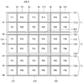
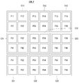
본 발명의 실시예에 따른 공통전극(COM)은 수개 또는 수십개 이상의 화소전극의 크기에 대응하는 크기를 갖도록 분할되는 복수의 터치전극들로 구성된다. 화소전극(P)은 게이트 라인들(G1~Gm)과 데이터 라인들(D1~Dn)의 교차에 의해 정의되는 영역에 할당된다. 설명의 편의를 위해 도 3 및 도 4에서는 공통전극(COM)이 가로 3개, 세로 3개, 총9개의 터치전극들(C11, C12, C13, C21, C22, C23, C31, C32, C33)로 분할되고, 이들 터치 전극 각각은 가로 2개, 세로 2개, 총 4개의 화소전극(P11, P12, P21, P22; P13, P14, P23, P24; P15, P16, P25, P26; P31, P32, P41, P42; P33, P34, P43, P44; P35, P36, P45, P46; P51, P52, P61, P62; P53, P54, P63, P64; P55, P56, P65, P66)의 크기에 대응하는 크기를 갖는 것으로 도시되어 있으나, 이는 하나의 예에 불과할 뿐 그 개수는 필요에 따라 얼마든지 변경될 수 있다. The common electrode COM according to an exemplary embodiment of the present invention includes a plurality of touch electrodes that are divided to have sizes corresponding to the sizes of several or tens or more pixel electrodes. The pixel electrode P is allocated to an area defined by the intersection of the gate lines G1 to Gm and the data lines D1 to Dn. For convenience of description, in FIGS. 3 and 4, the common electrode COM has three horizontal, three vertical, and nine touch electrodes C11, C12, C13, C21, C22, C23, C31, C32, and C33. Each of these touch electrodes is divided into two horizontal, two vertical, and four pixel electrodes P11, P12, P21, P22; P13, P14, P23, P24; P15, P16, P25, P26; P31, and P32. , P41, P42; P33, P34, P43, P44; P35, P36, P45, P46; P51, P52, P61, P62; P53, P54, P63, P64; P55, P56, P65, P66) Although shown as having a size, this is only one example, the number can be changed as needed.
공통전극(COM)을 구성하는 분할된 터치 전극들(C11, C12, C13, C21, C22, C23, C31, C32, C33)은 복수의 신호라인(TX11, TX12, TX13, TX21, TX22, TX23, TX31, TX32, TX33)에 의해 행단위 또는 열단위로 접속되며, 표시장치의 디스플레이를 구현하기 위한 구성요소 및 터치인식을 위한 터치센서의 구성요소로서의 기능을 동시에 수행한다. The divided touch electrodes C11, C12, C13, C21, C22, C23, C31, C32, and C33 constituting the common electrode COM have a plurality of signal lines TX11, TX12, TX13, TX21, TX22, TX23, TX31, TX32, and TX33 are connected in units of rows or columns, and simultaneously perform functions as components for implementing a display of a display device and components of a touch sensor for touch recognition.
도 5a는 본 발명의 제 1 실시예에 따른 터치 센서 일체형 표시장치의 공통전극(터치전극)과 신호라인의 연결관계의 일례를 도시한 도면, 도 5b는 본 발명의 제 1 실시예에 따른 터치 센서 일체형 표시장치의 공통전극(터치전극)과 신호라인의 연결관계의 다른 예를 도시한 도면이다. 5A illustrates an example of a connection relationship between a common electrode (touch electrode) and a signal line of a touch sensor integrated display device according to a first embodiment of the present invention, and FIG. 5B illustrates a touch according to the first embodiment of the present invention. Another example of a connection relationship between a common electrode (touch electrode) and a signal line of a sensor integrated display device is illustrated.
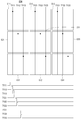
도 5a를 참조하면, 제 1 행에는 3개의 터치전극(C11, C12, C13)이 배열되고, 이들 3개의 터치전극의 각각은 제 1 행을 따라 배열된 제 1 내지 제 3 신호라인(TX11, TX12, TX13)의 각각에 접속되어 있다. 제 2 행에는 3개의 터치전극(C21, C22, C23)이 배열되고, 이들 3개의 터치전극의 각각은 제 2 행을 따라 배열된 제 4 내지 제 6 신호라인(TX21, TX22, TX23)의 각각에 접속되어 있다. 제 3 행에는 3개의 터치전극(C31, C32, C33)이 배열되고, 이들 3개의 터치전극의 각각은 제 3 행을 따라 배열된 제 1 내지 제 3 신호라인(TX31, TX32, TX33)의 각각에 접속되어 있다. 이와 같이 행방향을 따라 배열된 각각의 터치전극은 행 방향을 따라 배열된 하나의 신호라인에 연결되어 있으므로, 표시장치에 멀티 터치가 이루어지더라도 터치가 이루어진 위치를 정확하게 감지할 수 있다. Referring to FIG. 5A, three touch electrodes C11, C12, and C13 are arranged in a first row, and each of the three touch electrodes may include first to third signal lines TX11, arranged along a first row. Each of TX12 and TX13. Three touch electrodes C21, C22, and C23 are arranged in the second row, and each of these three touch electrodes is each of the fourth to sixth signal lines TX21, TX22, and TX23 arranged along the second row. Is connected to. Three touch electrodes C31, C32, and C33 are arranged in the third row, and each of the three touch electrodes is each of the first to third signal lines TX31, TX32, and TX33 arranged along the third row. Is connected to. As described above, each touch electrode arranged in the row direction is connected to one signal line arranged in the row direction, so that the touched position can be accurately sensed even if the display device is multi-touched.
도 5b를 참조하면, 도 5a와 마찬가지로 제 1 행에는 3개의 터치전극들(C11, C12, C13)이 배열되고, 이들 3개의 터치전극의 각각은 제 1 행을 따라 배열된 제 1 내지 제 3 신호라인(TX11, TX12, TX13)의 각각에 접속되어 있다. 다만, 도 5b의 실시예서는 제 1 내지 제 3 신호라인들(TX11, TX12, TX13)의 각각이 3개로 분지되어 각 신호라인을 구성하는 3개의 분지 신호라인이 하나의 터치전극에 접속되도록 구성된다는 점에서 도 5a와 다르다. 제 2 행의 터치전극(C21, C22, C23)과 제 3 내지 제 6 신호라인(TX21, TX22, TX23)의 접속관계 및 제 3 행의 터치전극(C31, C32, C33)과 제 3 신호라인(TX31, TX32, TX33)의 접속관계 또한 제 1 행의 터치전극과 제 1 내지 제 3 신호라인의 접속관계와 동일하므로 이에 대해서는 설명을 생략한다. Referring to FIG. 5B, similarly to FIG. 5A, three touch electrodes C11, C12, and C13 are arranged in the first row, and each of the three touch electrodes is arranged in the first to third rows along the first row. It is connected to each of the signal lines TX11, TX12, TX13. However, the embodiment of FIG. 5B is configured such that each of the first to third signal lines TX11, TX12, and TX13 is divided into three branches so that three branched signal lines constituting each signal line are connected to one touch electrode. It differs from FIG. 5A in that it is. Connection relationship between the touch electrodes C21, C22, and C23 of the second row and the third to sixth signal lines TX21, TX22, and TX23 and the touch electrodes C31, C32, C33 and the third signal line of the third row. Since the connection relationship between the TX31, TX32, and TX33 is the same as the connection relationship between the touch electrodes in the first row and the first to third signal lines, the description thereof will be omitted.
도 6a는 본 발명의 제 2 실시예에 따른 터치 센서 일체형 표시장치의 공통전극(터치전극)과 신호라인의 연결관계의 일례를 도시한 도면, 6b는 본 발명의 제 2 실시예에 따른 터치 센서 일체형 표시장치의 공통전극(터치전극)과 신호라인의 연결관계의 다른 예를 도시한 도면이다.6A is a diagram illustrating an example of a connection relationship between a common electrode (touch electrode) and a signal line of a touch sensor integrated display device according to a second embodiment of the present invention. FIG. 6B is a touch sensor according to a second embodiment of the present invention. Another example of a connection relationship between a common electrode (touch electrode) and a signal line of an integrated display device is illustrated.
도 6a 및 도 6b의 실시예는 터치전극들이 열 단위로 신호라인에 접속된다는 점에서 터치전극들이 행 단위로 신호라인에 접속되는 도 5a 및 도 5b의 실시예와 다르다. 6A and 6B differ from the embodiments of FIGS. 5A and 5B in which touch electrodes are connected to signal lines on a row basis in that touch electrodes are connected to signal lines on a column basis.
도 6a를 참조하면, 제 1 열에는 3개의 터치전극(C11, C21, C31)이 배열되고, 이들 3개의 터치전극의 각각은 제 1 열을 따라 배열된 제 1 내지 제 3 신호라인(TY11, TY12, TY13)의 각각에 접속되어 있다. 제 2 열에는 3개의 터치전극(C12, C22, C32)이 배열되고, 이들 3개의 터치전극의 각각은 제 2 열을 따라 배열된 제 4 내지 제 6 신호라인(TY21, TY22, TY23)의 각각에 접속되어 있다. 제 3 열에는 3개의 터치전극(C13, C23, C33)이 배열되고, 이들 3개의 터치전극의 각각은 제 3열을 따라 배열된 제 1 내지 제 3 신호라인(TY31, TY32, TY33)의 각각에 접속되어 있다. 이와 같이 열 방향으로 배열된 각각의 터치전극은 열 방향을 따라 배열된 하나의 신호라인에 연결되어 있으므로, 표시장치에 멀티 터치가 이루어지더라도 터치가 이루어진 위치를 정확하게 감지할 수 있다.Referring to FIG. 6A, three touch electrodes C11, C21, and C31 are arranged in a first column, and each of the three touch electrodes may include first to third signal lines TY11, which are arranged along the first column. TY12 and TY13, respectively. Three touch electrodes C12, C22, and C32 are arranged in the second column, and each of these three touch electrodes is each of the fourth to sixth signal lines TY21, TY22, and TY23 arranged along the second column. Is connected to. Three touch electrodes C13, C23, and C33 are arranged in the third column, and each of these three touch electrodes is each of the first to third signal lines TY31, TY32, and TY33 arranged along the third column. Is connected to. Since each touch electrode arranged in the column direction is connected to one signal line arranged in the column direction, the touched position can be accurately sensed even if the display device is multi-touched.
도 6b를 참조하면, 도 5a와 마찬가지로 제 1 열에는 3개의 터치전극들(C11, C21, C31)이 배열되고, 이들 3개의 터치전극의 각각은 제 1 열을 따라 배열된 제 1 내지 제 3 신호라인(TY11, TY12, TY13)의 각각에 접속되어 있다. 다만, 도 5b의 실시예서는 제 1 내지 제 3 신호라인들(TY11, TY12, TY13)의 각각이 3개로 분지되어 각 신호라인을 구성하는 3개의 분지 신호라인이 하나의 터치전극에 접속되도록 구성된다는 점에서 도 6a와 다르다. 제 2 열의 터치전극(C12, C22, C32)과 제 3 내지 제 6 신호라인(TY21, TY22, TY23)의 접속관계 및 제 3 열의 터치전극(C13, C23, C33)과 제 3 신호라인(TY31, TY32, TY33)의 접속관계 또한 제 1 열의 터치전극과 제 1 내지 제 3 신호라인의 접속관계와 동일하므로 이에 대해서는 설명을 생략한다. Referring to FIG. 6B, similar to FIG. 5A, three touch electrodes C11, C21, and C31 are arranged in the first column, and each of the three touch electrodes is arranged in the first to third rows along the first column. It is connected to each of the signal lines TY11, TY12, and TY13. However, in the embodiment of FIG. 5B, each of the first to third signal lines TY11, TY12, and TY13 is branched into three branches so that three branched signal lines constituting each signal line are connected to one touch electrode. It differs from FIG. 6A in that it is. Connection relationship between the touch electrodes C12, C22, and C32 of the second column and the third to sixth signal lines TY21, TY22, and TY23, and the touch electrodes C13, C23, C33 and the third signal line TY31 of the third column. , TY32 and TY33 are also the same as the connection between the touch electrodes in the first column and the first to third signal lines, and thus description thereof will be omitted.
이상 설명한 도 5a, 도 5b, 도 6a 및 도 6b의 실시예에서는 3행 3열로 이루어진 터치전극 구성에 대해 설명하고 있지만 이는 예시적인 사항에 지나지 않으며 본 발명이 이에 한정되는 것은 아니다. 예를 들어, 터치전극의 수와 터치전극에 접속되는 신호라인의 수는 터치전극의 크기 등 필요에 따라 적절히 조절할 수 있다. 또한, 각 터치 전극에는 적어도 하나의 신호라인이 접속될 수 있으며, 하나의 터치전극에 여러 개의 신호라인이 접속되도록 구성할 경우, 각 터치전극에 동일한 신호가 입출력되도록 이들 신호라인의 단부는 하나로 통합처리되는 것이 바람직하다.5A, 5B, 6A, and 6B described above, the configuration of the touch electrode having three rows and three columns is described, but this is only an example and the present invention is not limited thereto. For example, the number of touch electrodes and the number of signal lines connected to the touch electrodes can be appropriately adjusted as necessary, such as the size of the touch electrodes. In addition, at least one signal line may be connected to each touch electrode, and when a plurality of signal lines are connected to one touch electrode, the ends of these signal lines are integrated into one to input and output the same signal to each touch electrode. It is preferred to be treated.
도 7a는 본 발명의 제 1 실시예에 따른 터치 센서 일체형 표시장치의 일부분을 확대 도시한 평면도, 도 7b는 도 7a에 도시된 I-I' 라인 및 II-II'라인을 따라 취한 단면도이다. 도 7a 및 도 7b는 도 3에 도시된 공통전극(COM)의 터치 전극(C11) 중 화소전극(P11, P12)에 대응하는 영역을 예로 들어 도시한 평면도 및 단면도로서, 신호라인이 행방향으로 터치전극에 접속되는 경우의 예를 도시한 도면이다.7A is an enlarged plan view of a portion of a touch sensor integrated display device according to a first exemplary embodiment of the present invention, and FIG. 7B is a cross-sectional view taken along the line II ′ and II-II ′ of FIG. 7A. 7A and 7B are plan views and cross-sectional views illustrating regions corresponding to the pixel electrodes P11 and P12 of the touch electrode C11 of the common electrode COM illustrated in FIG. 3, for example, in which the signal lines are arranged in the row direction. It is a figure which shows the example in the case of connecting to a touch electrode.
도 7a 및 도 7b를 참조하면, 본 발명의 제 1 실시예에 따르는 터치 센서 일체형 표시장치는 제 1 기판(SUBS1) 상에 형성되는 게이트 라인(G1) 및 게이트 라인(G1)으로부터 연장되는 게이트 전극(G)과, 게이트 라인(G1)과 이격되어 평행하게 배치되는 제 1 신호라인(TX11)을 포함한다. 7A and 7B, the touch sensor integrated display device according to the first exemplary embodiment of the present invention may include a gate line G1 and a gate electrode extending from the gate line G1 formed on the first substrate SUBS1. (G) and a first signal line TX11 spaced apart from and parallel to the gate line G1.
또한, 상기 터치 센서 일체형 표시장치는 게이트 전극(G)을 구비하는 게이트 라인(G1) 및 제 1 신호라인(TX11)이 형성된 기판(SUBS1)상에 형성되는 게이트 절연막(GI)과, 게이트 전극(G)의 일부와 중첩되도록 게이트 절연막(GI) 상에 형성되는 반도체 패턴(A)을 포함한다. 반도체 패턴(A)은 후술하는 박막 트랜지스터(TFT)의 활성영역을 구성한다.In addition, the touch sensor integrated display device includes a gate insulating layer GI formed on a substrate SUBS1 on which a gate line G1 including a gate electrode G and a first signal line TX11 are formed, and a gate electrode ( A semiconductor pattern A is formed on the gate insulating film GI so as to overlap a part of G). The semiconductor pattern A constitutes an active region of the thin film transistor TFT described later.
또한, 상기 터치 센서 일체형 표시장치는 게이트 절연막(GI)을 사이에 두고 게이트 라인(G1)과 교차되는 데이터 라인(D1, D2), 데이터 라인(D1, D2)으로부터 연장된 소스 전극(S), 소스 전극(S)과 대향하는 드레인 전극(D)을 포함하는 박막 트랜지스터(TFT), 및 게이트 라인(G1)과 데이터 라인(D1)의 교차에 의해 정의되는 영역에 형성되며, 박막 트랜지스터(TFT)의 드레인 전극과 접속되는 화소전극(P11, P12)을 포함한다.In addition, the touch sensor integrated display device may include data lines D1 and D2 crossing the gate line G1, a source electrode S extending from the data lines D1 and D2, and having a gate insulating layer GI therebetween. The thin film transistor TFT including the drain electrode D facing the source electrode S, and the thin film transistor TFT formed in the region defined by the intersection of the gate line G1 and the data line D1. Pixel electrodes P11 and P12 connected to the drain electrodes of the transistors.
또한, 상기 터치 센서 일체형 표시장치는 데이터 라인(D1, D2)과 트랜지스터(TFT) 및 화소전극(P11, P12)이 형성된 게이트 절연막(GI)의 전면 상에 형성된 층간 절연막(INS)과, 층간 절연막(INS) 상에 형성되는 공통전극(터치전극)(C11)을 포함한다. 공통전극(터치전극)(C11)은 게이트 절연막과 층간절연막을 관통하는 콘택홀(CH)을 통해 제 1 신호라인(TX11)과 연결된다. In addition, the touch sensor integrated display device includes an interlayer insulating layer INS and an interlayer insulating layer formed on the entire surface of the gate insulating layer GI on which the data lines D1 and D2, the transistor TFT, and the pixel electrodes P11 and P12 are formed. And a common electrode (touch electrode) C11 formed on (INS). The common electrode (touch electrode) C11 is connected to the first signal line TX11 through a contact hole CH passing through the gate insulating layer and the interlayer insulating layer.
도 8a는 본 발명의 제 2 실시예에 따른 터치 센서 일체형 표시장치의 일부분을 확대 도시한 평면도, 도 8b는 도 8a에 도시된 III-III' 라인 및 IV-IV'라인을 따라 취한 단면도이다. 도 8a 및 도 8b는 도 3에 도시된 공통전극(COM)의 터치 전극(C11) 중 화소전극(P11, P12)에 대응하는 영역을 예로 들어 도시한 평면도 및 단면도로서, 신호라인이 열방향으로 터치전극에 접속되는 경우의 예를 도시한 도면이다.FIG. 8A is an enlarged plan view of a part of the touch sensor integrated type display apparatus according to the second embodiment of the present invention, and FIG. 8B is a sectional view taken along line III-III 'and line IV-IV' shown in FIG. 8A. 8A and 8B are plan views and cross-sectional views illustrating regions corresponding to the pixel electrodes P11 and P12 of the touch electrode C11 of the common electrode COM illustrated in FIG. 3 as an example, and the signal lines are arranged in the column direction. It is a figure which shows the example in the case of connecting to a touch electrode.
도 8a 및 도 8b를 참조하면, 본 발명의 제 2 실시예에 따르는 터치 센서 일체형 표시장치는 제 1 기판(SUBS1) 상에 형성되는 게이트 라인(G1) 및 게이트 라인(G1)으로부터 연장되는 게이트 전극(G)을 포함한다. 8A and 8B, the touch sensor integrated display device according to the second exemplary embodiment of the present invention includes a gate line G1 and a gate electrode extending from the gate line G1 formed on the first substrate SUBS1. (G).
또한, 상기 터치 센서 일체형 표시장치는 게이트 전극(G)을 구비하는 게이트 라인(G1)이 형성된 기판(SUBS1)상에 형성되는 게이트 절연막(GI)과, 게이트 전극(G)의 일부와 중첩되도록 게이트 절연막(GI) 상에 형성되는 반도체 패턴(A)을 포함한다. 반도체 패턴(A)은 후술하는 박막 트랜지스터(TFT)의 활성영역을 구성한다.In addition, the touch sensor integrated display device may include a gate insulating layer GI formed on the substrate SUBS1 on which the gate line G1 including the gate electrode G is formed, and a gate overlapping a portion of the gate electrode G. The semiconductor pattern A is formed on the insulating film GI. The semiconductor pattern A constitutes an active region of the thin film transistor TFT described later.
또한, 상기 터치 센서 일체형 표시장치는 게이트 절연막(GI)을 사이에 두고 게이트 라인(G1)과 교차되는 데이터 라인(D1, D2), 데이터 라인(D1, D2)으로부터 연장된 소스 전극(S), 소스 전극(S)과 대향하는 드레인 전극(D)을 포함하는 박막 트랜지스터(TFT), 상기 데이터 라인(D1, D2)으로부터 이격되어 데이터 라인(D1, D2)과 평행하게 형성되는 제 1 신호라인(TY11) 및 제 2 신호라인(TY12), 게이트 라인(G1)과 데이터 라인(D1)의 교차에 의해 정의되는 영역에 형성되며, 박막 트랜지스터(TFT)의 드레인 전극과 접속되는 화소전극(P11, P12)을 포함한다.In addition, the touch sensor integrated display device may include data lines D1 and D2 crossing the gate line G1, a source electrode S extending from the data lines D1 and D2, and having a gate insulating layer GI therebetween. A thin film transistor TFT including a drain electrode D facing the source electrode S, and a first signal line spaced apart from the data lines D1 and D2 and formed in parallel with the data lines D1 and D2. The pixel electrodes P11 and P12 formed in the region defined by the intersection of the TY11, the second signal line TY12, the gate line G1 and the data line D1, and connected to the drain electrode of the thin film transistor TFT. ).
또한, 상기 터치 센서 일체형 표시장치는 데이터 라인(D1, D2)과 트랜지스터(TFT) 및 화소전극(P11, P12)이 형성된 게이트 절연막(GI)의 전면 상에 형성된 층간 절연막(INS)과, 층간 절연막(INS) 상에 형성되는 공통전극(터치전극)(C11)을 포함한다. 공통전극(터치전극)(C11)은 층간절연막(INS)을 관통하는 콘택홀(CH)을 통해 제 2 신호라인(TY12)과 연결된다.In addition, the touch sensor integrated display device includes an interlayer insulating layer INS and an interlayer insulating layer formed on the entire surface of the gate insulating layer GI on which the data lines D1 and D2, the transistor TFT, and the pixel electrodes P11 and P12 are formed. And a common electrode (touch electrode) C11 formed on (INS). The common electrode (touch electrode) C11 is connected to the second signal line TY12 through a contact hole CH passing through the interlayer insulating layer INS.
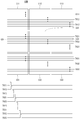
다음으로 본 발명의 실시예에 따르는 터치 센서 일체형 액정 표시장치의 동작에 대해 설명하기로 한다. 이하의 설명에서는 60Hz 시분할 구동의 예를 들어 설명하기로 한다. Next, an operation of the touch sensor integrated liquid crystal display according to the exemplary embodiment will be described. In the following description, an example of 60 Hz time division driving will be described.
본 발명의 실시예에 따르는 터치 센서 일체형 액정 표시장치는 시분할로 구동된다. 또한, 시분할 구동의 1주기는 도 9에 도시된 바와 같이 디스플레이 구간과 터치 구간으로 구성되어 있으며, 디스플레이 시에는 터치 구동이 오프되고, 터치 시에는 디스플레이 구동이 오프되어 상호 간의 신호간섭이 최소화되도록 되어 있다. 일례로 60Hz 시분할 구동에서는 16.7ms가 1주기가 되며, 이를 디스플레이 구동 구간(약 10ms)과 터치 구동 구간(약 6.7ms)으로 나누어 사용하게 된다. The touch sensor integrated liquid crystal display according to the embodiment of the present invention is driven by time division. In addition, one cycle of time division driving is composed of a display section and a touch section, as shown in FIG. have. For example, in 60Hz time division driving, 16.7ms is one cycle, and this is divided into a display driving section (about 10ms) and a touch driving section (about 6.7ms).
디스플레이 구간에서 호스트 콘트롤러(100)는 전원 공급부(105)를 제어하여 예를 들면 터치전극들(C11~C33)로 구성되는 공통전극(COM)에 예를 들면 도 5a의 신호라인들(TX11~TX33) 또는 도 6a의 신호라인들(TY11~TY33)을 통해 공통전압(Vcom)을 동시에 공급하고, 데이터 구동부(102)는 게이트 구동부(103)로부터 순차적으로 출력되는 게이트 펄스(Gate)에 동기되어 데이터 라인(D1~Dn)을 통해 화소전극(P11~P66)에 디지털 비디오 데이터에 대응하는 화소전압(Data)을 공급한다. 이와 같이 화소전극(P11~P66)과 공통전극(COM)에 각각 인가되는 공통전압(Vcom)과 화소전압(Data)에 의해 액정층에 전계가 형성되므로, 이 전계에 의해 액정 상태가 변화되어 디스플레이 동작이 수행된다. 이 때 각각의 신호라인(TX11~TX33)에 의해 복수의 터치전극(C11~C33)에 접속된 터치 인식 프로세서(107)는 터치전극들(C11~C33) 각각의 초기 정전용량의 전압값을 측정하여 저장한다. In the display period, the
다음으로, 터치 구동 구간에서 호스트 콘트롤러(100)는 전원 공급부(105)를 제어하여, 예를 들면 도 5a 및 도 5b의 신호라인들(TX11~TX33) 또는 도 6a 및 도 6b의 신호라인들(TY11~TY33)을 통해 공통전극(COM)을 구성하는 터치전극들(C11~C33)에 터치 구동전압(Vtsp)을 순차적으로 공급하도록 한다. 복수의 터치전극들(C11~C33)에 접속된 터치 인식 프로세서(107)는 저장된 터치전극들(C11~C33)의 각각의 초기 정전용량의 전압과 터치 구동구간에서 측정된 정전용량의 전압(Vd)을 차동 증폭하고 그 결과를 디지털 데이터로 변환한다. 또한, 터치 인식 프로세서(107)는 터치 인식 알고리즘을 이용하여 초기 정전용량과 터치 정전용량의 차이를 바탕으로 터치가 이루어진 터치 위치를 판단하고, 그 터치 위치를 지시하는 터치 좌표 데이터를 출력한다. Next, in the touch driving period, the
상기 터치 센서 일체형 액정 표시장치는 디스플레이 구동시에는 터치 구동이 오프되어 게이트 라인(GL) 및 데이터 라인(DL)에 신호공급이 중단되고, 터치 구동시에는 디스플레이 구동이 오프되어, 공통전압(Vcom)이 공급되지 않는 시분할 구동으로 구동된다. In the touch sensor integrated liquid crystal display, when the display is driven, the touch driving is turned off to stop the signal supply to the gate line GL and the data line DL, and when the touch driving is performed, the display driving is turned off and the common voltage Vcom It is driven by time division driving which is not supplied.
상술한 본 발명의 실시예에 의한 터치 센서 일체형 표시장치에 따르면, 터치를 인식하기 위한 터치 센서를 표시장치의 구성요소와 겸용할 수 있게 되므로 표시장치의 두께를 얇게 하는 동시에 내구성을 향상시킬 수 있는 효과를 얻을 수 있다.According to the touch sensor integrated display device according to the embodiment of the present invention described above, the touch sensor for recognizing a touch can be used as a component of the display device, thereby reducing the thickness of the display device and improving durability. The effect can be obtained.
또한, 본 발명의 실시예에 의한 터치 센서 일체형 표시장치에 따르면, 터치 인식을 위한 터치 구동라인과 터치센싱 라인을 별도로 구성할 필요가 없기 때문에 신호라인의 수를 줄일 수 있어 간단한 배선구조로 멀티 터치를 인식할 수 있는 효과를 얻을 수 있다.In addition, according to the touch sensor integrated display device according to an exemplary embodiment of the present invention, since the touch driving line and the touch sensing line for touch recognition do not need to be separately configured, the number of signal lines can be reduced, and thus, multi-touch with a simple wiring structure. You can get the effect that can recognize.
본 발명의 실시예에 의한 터치 센서 일체형 표시장치에 따르면 기생 정전용량에 의한 노이즈 문제를 해소시킬 수 있으므로 상호 정전용량방식에 비해 정전용량의 레벨을 높일 수 있어 멀티 터치 인식의 정밀도를 높일 수 있는 효과를 얻을 수 있다.According to the touch sensor integrated display device according to the embodiment of the present invention, the noise problem due to the parasitic capacitance can be solved, and thus the level of capacitance can be increased compared to the mutual capacitance method, thereby increasing the accuracy of multi-touch recognition. Can be obtained.
본 발명의 실시예에 의한 터치 센서 일체형 표시장치에 따르면 상호정전용량 방식에 비해 터치인식을 위한 신호라인의 수를 줄일 수 있으므로 배선구조를 간단히 할 수 있는 효과를 얻을 수 있다.According to the touch sensor-integrated display device according to the embodiment of the present invention, the number of signal lines for touch recognition can be reduced compared to the mutual capacitance method, so that the wiring structure can be simplified.
이상 설명한 내용을 통해 당업자라면 본 발명의 기술사상을 일탈하지 아니하는 범위에서 다양한 변경 및 수정이 가능함을 알 수 있을 것이다. 예를 들어, 본 발명의 실시예에 설명하고 있는 제 1 방향이나 제 2 방향은 서로 반대되는 방향으로 변경하는 것이 가능하고, 공통전극의 크기 및 수와 형상, 공통전극을 구성하는 터치전극의 크기 및 수와 형상, 각각의 터치전극과 접속되는 신호라인의 수는 임의로 적절히 변경할 수 있는 사항이며, 본 발명의 실시예에 기재된 것으로 한정되는 것은 아니다. 따라서, 본 발명의 기술적 범위는 발명의 상세한 설명에 기재된 내용으로 한정되는 것이 아니라 특허 청구의 범위에 의해 정하여져야만 할 것이다.
It will be apparent to those skilled in the art that various modifications and variations can be made in the present invention without departing from the spirit or scope of the invention. For example, the first direction and the second direction described in the embodiment of the present invention can be changed in directions opposite to each other, and the size and number and shape of the common electrodes, and the size of the touch electrodes constituting the common electrode. And the number and shape and the number of signal lines connected to each touch electrode can be arbitrarily changed appropriately, and are not limited to those described in the embodiments of the present invention. Therefore, the technical scope of the present invention should not be limited to the contents described in the detailed description of the invention but should be defined by the claims.
100 : 호스트 콘트롤러 101 : 타이밍 콘트롤러
102 : 데이터 구동부 103 : 게이트 구동부
105 : 전원 공급부 107 : 터치 인식 프로세서
CFA : 컬러필터 어레이 TFTA : 박막 트랜지스터 어레이
Vcom : 공통전압 Vtsp : 터치 구동전압100: host controller 101: timing controller
102: data driver 103: gate driver
105: power supply unit 107: touch recognition processor
CFA: Color Filter Array TFTA: Thin Film Transistor Array
Vcom: Common Voltage Vtsp: Touch Driving Voltage
Claims (6)
상기 게이트 라인과 상기 데이터 라인의 교차에 의해 정의되는 영역에 형성되는 복수의 화소전극들; 및
절연층을 사이에 두고 상기 복수의 화소전극들과 중첩되도록 형성되는 공통전극을 포함하며,
상기 공통전극은 적어도 2이상의 터치전극을 포함하며,
상기 터치전극의 각각은 제 1 방향 및 상기 제 1 방향과 교차하는 제 2 방향 중 어느 한 방향으로 배열되는 적어도 하나의 신호선에 접속되는 것을 특징으로 하는 터치센서 일체형 표시장치.
A gate line and a data line formed to cross each other on the substrate;
A plurality of pixel electrodes formed in an area defined by the intersection of the gate line and the data line; And
A common electrode formed to overlap the plurality of pixel electrodes with an insulating layer interposed therebetween,
The common electrode includes at least two touch electrodes,
And each of the touch electrodes is connected to at least one signal line arranged in one of a first direction and a second direction crossing the first direction.
상기 게이트라인과 이격되어 상기 기판 상에서 상기 게이트 라인과 평행하게 형성되는 신호라인과;
상기 게이트라인과 상기 신호라인이 형성된 기판의 전면 상에 형성되는 게이트 절연막;
상기 게이트라인과 교차하도록 상기 게이트 절연막 상에 형성되는 데이터 라인;
상기 게이트 절연막 상에 형성되며 상기 데이터 라인에 접속되는 소스전극을 구비하는 박막 트랜지스터;
상기 박막 트랜지스터의 드레인 전극에 접속되도록 상기 게이트 절연막 상에 형성되는 화소전극;
상기 데이터 라인, 상기 박막트랜지스터 및 상기 화소전극이 형성된 게이트 절연막 상에 형성되며, 상기 게이트 라인과 상기 데이터 라인의 교차에 의해 정의되는 영역에 형성되는 층간절연막;
상기 층간절연막 상에 형성되며 상기 층간절연막에 형성된 콘택홀을 통해 상기 신호라인에 접속되는 공통전극을 포함하며,
상기 공통전극은 적어도 2이상의 터치전극을 포함하며, 상기 터치전극의 각각은 상기 신호선에 접속되는 것을 특징으로 하는 터치센서 일체형 표시장치.
A gate line formed on the substrate;
A signal line spaced apart from the gate line and formed parallel to the gate line on the substrate;
A gate insulating film formed on an entire surface of the substrate on which the gate line and the signal line are formed;
A data line formed on the gate insulating layer to cross the gate line;
A thin film transistor formed on the gate insulating film and having a source electrode connected to the data line;
A pixel electrode formed on the gate insulating film so as to be connected to the drain electrode of the thin film transistor;
An interlayer insulating film formed on the gate insulating film on which the data line, the thin film transistor, and the pixel electrode are formed, and formed in a region defined by the intersection of the gate line and the data line;
A common electrode formed on the interlayer insulating layer and connected to the signal line through a contact hole formed in the interlayer insulating layer;
The common electrode includes at least two touch electrodes, and each of the touch electrodes is connected to the signal line.
상기 게이트라인이 형성된 기판의 전면 상에 형성되는 게이트 절연막;
상기 게이트라인과 교차하도록 상기 게이트 절연막 상에 형성되는 데이터 라인;
상기 게이트라인과 교차하도록 상기 게이트 절연막 상에 형성되며 상기 데이터 라인과 이격되어 상기 데이터 라인과 평행하게 형성되는 신호라인;
상기 게이트 절연막 상에 형성되며 상기 데이터 라인에 접속되는 소스전극을 구비하는 박막 트랜지스터;
상기 박막 트랜지스터의 드레인 전극에 접속되도록 상기 게이트 절연막 상에 형성되며, 상기 게이트 라인과 상기 데이터 라인의 교차에 의해 정의되는 영역에 형성되는 화소전극;
상기 데이터 라인, 상기 신호라인, 상기 박막트랜지스터 및 상기 화소전극이 형성된 게이트 절연막 상에 형성되는 층간절연막;
상기 층간절연막 상에 형성되며 상기 층간절연막에 형성된 콘택홀을 통해 상기 신호라인에 접속되는 공통전극을 포함하며,
상기 공통전극은 적어도 2이상의 터치전극을 포함하며, 상기 터치전극의 각각은 상기 신호선에 접속되는 것을 특징으로 하는 터치센서 일체형 표시장치.
A gate line formed on the substrate;
A gate insulating film formed on an entire surface of the substrate on which the gate line is formed;
A data line formed on the gate insulating layer to cross the gate line;
A signal line formed on the gate insulating layer to cross the gate line and spaced apart from the data line to be parallel to the data line;
A thin film transistor formed on the gate insulating film and having a source electrode connected to the data line;
A pixel electrode formed on the gate insulating film so as to be connected to the drain electrode of the thin film transistor, and formed in a region defined by the intersection of the gate line and the data line;
An interlayer insulating film formed on the gate insulating film on which the data line, the signal line, the thin film transistor and the pixel electrode are formed;
A common electrode formed on the interlayer insulating layer and connected to the signal line through a contact hole formed in the interlayer insulating layer;
The common electrode includes at least two touch electrodes, and each of the touch electrodes is connected to the signal line.
상기 터치전극의 각각은 적어도 2이상의 화소전극에 대응하는 크기를 갖는 것을 특징으로 터치센서 일체형 표시장치.
The method according to any one of claims 1 to 3,
And each of the touch electrodes has a size corresponding to at least two pixel electrodes.
상기 터치 센서 일체형 표시장치는 디스플레이 구동시에는 터치 구동이 오프되고, 터치 구동시에는 디스플레이 구동이 오프되는 시분할로 구동되는 것을 특징으로 하는 터치 센서 일체형 표시장치.
The method according to any one of claims 1 to 3,
The touch sensor integrated display device is driven by a time division in which the touch drive is turned off when the display is driven and the display drive is turned off when the display is driven.
상기 디스플레이 구동시에는 상기 신호선을 통해 상기 2이상의 터치전극에 동일한 공통전압이 공급되고, 상기 터치 구동시에는 상기 터치 전극에 순차적으로 터치 구동전압이 공급되는 것을 특징으로 하는 터치 센서 일체형 표시장치.The method of claim 5, wherein
And the same common voltage is supplied to the two or more touch electrodes through the signal line during the display driving, and the touch driving voltage is sequentially supplied to the touch electrodes during the touch driving.
Priority Applications (11)
| Application Number | Priority Date | Filing Date | Title |
|---|---|---|---|
| KR1020110017181A KR101457743B1 (en) | 2011-02-25 | 2011-02-25 | Touch sensor integrated display device |
| CN201110447655.XA CN102650916B (en) | 2011-02-25 | 2011-12-23 | Touch sensor integrated display device |
| EP11195553.0A EP2492784B1 (en) | 2011-02-25 | 2011-12-23 | Touch sensor integrated display device |
| TW100148930A TWI464854B (en) | 2011-02-25 | 2011-12-27 | Touch sensor integrated display device |
| US13/337,390 US9250735B2 (en) | 2011-02-25 | 2011-12-27 | Touch sensor integrated display device |
| US14/981,550 US9639205B2 (en) | 2011-02-25 | 2015-12-28 | Touch sensor integrated display device |
| US15/157,305 US10180750B2 (en) | 2011-02-25 | 2016-05-17 | Touch sensor integrated display device |
| US16/202,024 US10649575B2 (en) | 2011-02-25 | 2018-11-27 | Touch sensor integrated display device |
| US16/847,118 US11157123B2 (en) | 2011-02-25 | 2020-04-13 | Touch sensor integrated display device |
| US17/510,363 US11740749B2 (en) | 2011-02-25 | 2021-10-25 | Touch sensor integrated display device |
| US18/221,490 US20230359313A1 (en) | 2011-02-25 | 2023-07-13 | Touch display device |
Applications Claiming Priority (1)
| Application Number | Priority Date | Filing Date | Title |
|---|---|---|---|
| KR1020110017181A KR101457743B1 (en) | 2011-02-25 | 2011-02-25 | Touch sensor integrated display device |
Publications (2)
| Publication Number | Publication Date |
|---|---|
| KR20120097765A true KR20120097765A (en) | 2012-09-05 |
| KR101457743B1 KR101457743B1 (en) | 2014-11-04 |
Family
ID=47108925
Family Applications (1)
| Application Number | Title | Priority Date | Filing Date |
|---|---|---|---|
| KR1020110017181A KR101457743B1 (en) | 2011-02-25 | 2011-02-25 | Touch sensor integrated display device |
Country Status (1)
| Country | Link |
|---|---|
| KR (1) | KR101457743B1 (en) |
Cited By (23)
| Publication number | Priority date | Publication date | Assignee | Title |
|---|---|---|---|---|
| KR101318448B1 (en) * | 2012-12-11 | 2013-10-16 | 엘지디스플레이 주식회사 | Touch sensor integrated type display device and method of fabricating the same |
| KR20140001710U (en) * | 2012-09-14 | 2014-03-24 | 수퍼씨-터치 코퍼레이션 | In-cell touch display panel system using metal wires to connect with sensing electrodes |
| KR101380479B1 (en) * | 2012-03-30 | 2014-04-01 | 엘지디스플레이 주식회사 | Touch screen integrated display device and method of fabricating the same |
| KR20140060978A (en) * | 2012-11-13 | 2014-05-21 | 엘지디스플레이 주식회사 | Display device with integrated touch screen |
| KR20140076850A (en) * | 2012-12-13 | 2014-06-23 | 엘지디스플레이 주식회사 | Touch sensor integrated type display device |
| KR20140076845A (en) * | 2012-12-13 | 2014-06-23 | 엘지디스플레이 주식회사 | Touch sensor integrated type display device |
| KR20140076841A (en) * | 2012-12-13 | 2014-06-23 | 엘지디스플레이 주식회사 | Touch sensor integrated type display device |
| KR20140078420A (en) * | 2012-12-17 | 2014-06-25 | 엘지디스플레이 주식회사 | Touch sensor integrated type display device |
| KR101455314B1 (en) * | 2012-11-19 | 2014-10-27 | 엘지디스플레이 주식회사 | Display device with integrated touch screen |
| KR20150030539A (en) * | 2013-09-12 | 2015-03-20 | 엘지디스플레이 주식회사 | In cell touch liquid crystal display device |
| KR20150041222A (en) * | 2013-10-04 | 2015-04-16 | 삼성디스플레이 주식회사 | Display device comprising touch sensors |
| KR20150058642A (en) * | 2013-11-19 | 2015-05-29 | 엘지디스플레이 주식회사 | Display device and driving method thereof |
| KR20150060279A (en) * | 2013-11-26 | 2015-06-03 | 엘지디스플레이 주식회사 | Touch and gesture sensing system and driving method thereof |
| KR101539330B1 (en) * | 2014-04-30 | 2015-07-30 | 엘지디스플레이 주식회사 | Display Panel For Display Device |
| KR20160019626A (en) * | 2014-08-11 | 2016-02-22 | 엘지디스플레이 주식회사 | Touch sensor integrated type display device |
| KR20160064224A (en) * | 2013-09-30 | 2016-06-07 | 시냅틱스 인코포레이티드 | Matrix sensor for image touch sensing |
| KR20160080959A (en) * | 2014-12-30 | 2016-07-08 | 엘지디스플레이 주식회사 | Touch display apparatus |
| KR20170081098A (en) * | 2015-12-31 | 2017-07-11 | 엘지디스플레이 주식회사 | Display device with a built-in touch screen and method for fabricating the same |
| EP3151089A4 (en) * | 2014-05-30 | 2018-01-10 | Boe Technology Group Co. Ltd. | Embedded touchscreen and display device |
| EP3151090A4 (en) * | 2014-05-30 | 2018-01-10 | BOE Technology Group Co., Ltd. | Embedded touchscreen and display apparatus |
| KR20180046865A (en) * | 2016-10-28 | 2018-05-09 | 엘지디스플레이 주식회사 | Touch sensor integrated type electroluminescent desplay device |
| US10067614B2 (en) | 2014-05-30 | 2018-09-04 | Boe Technology Group Co., Ltd. | In-cell touch panel and display device |
| KR20220087422A (en) * | 2015-01-30 | 2022-06-24 | 엘지디스플레이 주식회사 | Touch Display Device |
Families Citing this family (1)
| Publication number | Priority date | Publication date | Assignee | Title |
|---|---|---|---|---|
| KR20230049188A (en) | 2021-10-05 | 2023-04-13 | 삼성디스플레이 주식회사 | Display device and driving method of the same |
Family Cites Families (1)
| Publication number | Priority date | Publication date | Assignee | Title |
|---|---|---|---|---|
| US8217913B2 (en) | 2009-02-02 | 2012-07-10 | Apple Inc. | Integrated touch screen |
-
2011
- 2011-02-25 KR KR1020110017181A patent/KR101457743B1/en active IP Right Grant
Cited By (28)
| Publication number | Priority date | Publication date | Assignee | Title |
|---|---|---|---|---|
| KR101380479B1 (en) * | 2012-03-30 | 2014-04-01 | 엘지디스플레이 주식회사 | Touch screen integrated display device and method of fabricating the same |
| US9164306B2 (en) | 2012-09-14 | 2015-10-20 | Superc-Touch Corporation | In-cell touch display panel system using metal wires to connect with sensing electrodes |
| KR20140001710U (en) * | 2012-09-14 | 2014-03-24 | 수퍼씨-터치 코퍼레이션 | In-cell touch display panel system using metal wires to connect with sensing electrodes |
| KR20140060978A (en) * | 2012-11-13 | 2014-05-21 | 엘지디스플레이 주식회사 | Display device with integrated touch screen |
| US9256309B2 (en) | 2012-11-13 | 2016-02-09 | Lg Display Co., Ltd. | Display device including integrated touch panel |
| KR101455314B1 (en) * | 2012-11-19 | 2014-10-27 | 엘지디스플레이 주식회사 | Display device with integrated touch screen |
| KR101318448B1 (en) * | 2012-12-11 | 2013-10-16 | 엘지디스플레이 주식회사 | Touch sensor integrated type display device and method of fabricating the same |
| US9535523B2 (en) | 2012-12-11 | 2017-01-03 | Lg Display Co., Ltd. | Touch sensor integrated type display device |
| KR20140076850A (en) * | 2012-12-13 | 2014-06-23 | 엘지디스플레이 주식회사 | Touch sensor integrated type display device |
| KR20140076845A (en) * | 2012-12-13 | 2014-06-23 | 엘지디스플레이 주식회사 | Touch sensor integrated type display device |
| KR20140076841A (en) * | 2012-12-13 | 2014-06-23 | 엘지디스플레이 주식회사 | Touch sensor integrated type display device |
| KR20140078420A (en) * | 2012-12-17 | 2014-06-25 | 엘지디스플레이 주식회사 | Touch sensor integrated type display device |
| KR20150030539A (en) * | 2013-09-12 | 2015-03-20 | 엘지디스플레이 주식회사 | In cell touch liquid crystal display device |
| KR20200103122A (en) * | 2013-09-30 | 2020-09-01 | 시냅틱스 인코포레이티드 | Matrix sensor for image touch sensing |
| KR20160064224A (en) * | 2013-09-30 | 2016-06-07 | 시냅틱스 인코포레이티드 | Matrix sensor for image touch sensing |
| KR20150041222A (en) * | 2013-10-04 | 2015-04-16 | 삼성디스플레이 주식회사 | Display device comprising touch sensors |
| KR20150058642A (en) * | 2013-11-19 | 2015-05-29 | 엘지디스플레이 주식회사 | Display device and driving method thereof |
| KR20150060279A (en) * | 2013-11-26 | 2015-06-03 | 엘지디스플레이 주식회사 | Touch and gesture sensing system and driving method thereof |
| KR101539330B1 (en) * | 2014-04-30 | 2015-07-30 | 엘지디스플레이 주식회사 | Display Panel For Display Device |
| EP3151089A4 (en) * | 2014-05-30 | 2018-01-10 | Boe Technology Group Co. Ltd. | Embedded touchscreen and display device |
| US10067614B2 (en) | 2014-05-30 | 2018-09-04 | Boe Technology Group Co., Ltd. | In-cell touch panel and display device |
| EP3151090A4 (en) * | 2014-05-30 | 2018-01-10 | BOE Technology Group Co., Ltd. | Embedded touchscreen and display apparatus |
| US9619066B2 (en) | 2014-08-11 | 2017-04-11 | Lg Display Co., Ltd. | Touch sensor integrated type display device |
| KR20160019626A (en) * | 2014-08-11 | 2016-02-22 | 엘지디스플레이 주식회사 | Touch sensor integrated type display device |
| KR20160080959A (en) * | 2014-12-30 | 2016-07-08 | 엘지디스플레이 주식회사 | Touch display apparatus |
| KR20220087422A (en) * | 2015-01-30 | 2022-06-24 | 엘지디스플레이 주식회사 | Touch Display Device |
| KR20170081098A (en) * | 2015-12-31 | 2017-07-11 | 엘지디스플레이 주식회사 | Display device with a built-in touch screen and method for fabricating the same |
| KR20180046865A (en) * | 2016-10-28 | 2018-05-09 | 엘지디스플레이 주식회사 | Touch sensor integrated type electroluminescent desplay device |
Also Published As
| Publication number | Publication date |
|---|---|
| KR101457743B1 (en) | 2014-11-04 |
Similar Documents
| Publication | Publication Date | Title |
|---|---|---|
| KR101457743B1 (en) | Touch sensor integrated display device | |
| KR101450948B1 (en) | Touch sensor integrated display device | |
| US20220113840A1 (en) | Touch sensor integrated display device | |
| EP2985682B1 (en) | Touch sensor integrated type display device | |
| US10712878B2 (en) | Touch sensor integrated type display device | |
| JP6446510B2 (en) | Touch panel and driving device thereof | |
| KR101671578B1 (en) | Touch sensor integrated type display device | |
| KR101735386B1 (en) | Liquid crystal display device having touch sensor embedded therein, method for driving the same and method for fabricating the same | |
| KR101681806B1 (en) | Touch sensor integrated type display device | |
| US9952694B2 (en) | Display device integrated with touch screen | |
| US8891048B2 (en) | Liquid crystal display with integrated touch screen panel and driving method thereof | |
| EP2447814B1 (en) | Liquid crystal display with integrated touch screen panel and driving method thereof | |
| TWI591526B (en) | Touch sensor integrated type display device | |
| KR20120097761A (en) | Touch integrated display device | |
| KR101723879B1 (en) | Display device with integrated touch screen | |
| KR102040654B1 (en) | Touch sensor integrated type display device and method of fabricating the same | |
| KR101675848B1 (en) | Liquid crystal display device having touch sensor embedded therein |
Legal Events
| Date | Code | Title | Description |
|---|---|---|---|
| A201 | Request for examination | ||
| E902 | Notification of reason for refusal | ||
| E701 | Decision to grant or registration of patent right | ||
| GRNT | Written decision to grant | ||
| FPAY | Annual fee payment |
Payment date: 20180917 Year of fee payment: 5 |
|
| FPAY | Annual fee payment |
Payment date: 20190917 Year of fee payment: 6 |