KR20120095225A - Copper electroplating solution and method of copper electroplating using the same - Google Patents
Copper electroplating solution and method of copper electroplating using the same Download PDFInfo
- Publication number
- KR20120095225A KR20120095225A KR1020110014764A KR20110014764A KR20120095225A KR 20120095225 A KR20120095225 A KR 20120095225A KR 1020110014764 A KR1020110014764 A KR 1020110014764A KR 20110014764 A KR20110014764 A KR 20110014764A KR 20120095225 A KR20120095225 A KR 20120095225A
- Authority
- KR
- South Korea
- Prior art keywords
- copper plating
- additive
- plating solution
- copper
- present
- Prior art date
Links
- 239000010949 copper Substances 0.000 title claims abstract description 282
- RYGMFSIKBFXOCR-UHFFFAOYSA-N Copper Chemical compound [Cu] RYGMFSIKBFXOCR-UHFFFAOYSA-N 0.000 title claims abstract description 275
- 229910052802 copper Inorganic materials 0.000 title claims abstract description 275
- 238000000034 method Methods 0.000 title claims abstract description 68
- 238000009713 electroplating Methods 0.000 title 2
- 238000007747 plating Methods 0.000 claims abstract description 275
- 239000000654 additive Substances 0.000 claims abstract description 116
- 230000000996 additive effect Effects 0.000 claims abstract description 107
- XLYOFNOQVPJJNP-UHFFFAOYSA-N water Substances O XLYOFNOQVPJJNP-UHFFFAOYSA-N 0.000 claims abstract description 21
- AFVFQIVMOAPDHO-UHFFFAOYSA-N Methanesulfonic acid Chemical compound CS(O)(=O)=O AFVFQIVMOAPDHO-UHFFFAOYSA-N 0.000 claims description 53
- VEXZGXHMUGYJMC-UHFFFAOYSA-M Chloride anion Chemical compound [Cl-] VEXZGXHMUGYJMC-UHFFFAOYSA-M 0.000 claims description 30
- 150000001875 compounds Chemical class 0.000 claims description 30
- 239000000758 substrate Substances 0.000 claims description 26
- 229940098779 methanesulfonic acid Drugs 0.000 claims description 25
- 238000006116 polymerization reaction Methods 0.000 claims description 22
- 239000000463 material Substances 0.000 claims description 19
- 239000003795 chemical substances by application Substances 0.000 claims description 17
- 229910052739 hydrogen Inorganic materials 0.000 claims description 17
- 239000001257 hydrogen Substances 0.000 claims description 16
- 125000000217 alkyl group Chemical group 0.000 claims description 15
- SDFNZYMSEOUVIF-UHFFFAOYSA-N copper;methanesulfonic acid Chemical compound [Cu].CS(O)(=O)=O SDFNZYMSEOUVIF-UHFFFAOYSA-N 0.000 claims description 15
- FAPWRFPIFSIZLT-UHFFFAOYSA-M Sodium chloride Chemical compound [Na+].[Cl-] FAPWRFPIFSIZLT-UHFFFAOYSA-M 0.000 claims description 12
- 125000004435 hydrogen atom Chemical group [H]* 0.000 claims description 12
- VEXZGXHMUGYJMC-UHFFFAOYSA-N Hydrochloric acid Chemical compound Cl VEXZGXHMUGYJMC-UHFFFAOYSA-N 0.000 claims description 7
- 238000011049 filling Methods 0.000 claims description 6
- 238000009499 grossing Methods 0.000 claims description 6
- 239000011780 sodium chloride Substances 0.000 claims description 6
- 229910000041 hydrogen chloride Inorganic materials 0.000 claims description 5
- IXCSERBJSXMMFS-UHFFFAOYSA-N hydrogen chloride Substances Cl.Cl IXCSERBJSXMMFS-UHFFFAOYSA-N 0.000 claims description 5
- DGAQECJNVWCQMB-PUAWFVPOSA-M Ilexoside XXIX Chemical compound C[C@@H]1CC[C@@]2(CC[C@@]3(C(=CC[C@H]4[C@]3(CC[C@@H]5[C@@]4(CC[C@@H](C5(C)C)OS(=O)(=O)[O-])C)C)[C@@H]2[C@]1(C)O)C)C(=O)O[C@H]6[C@@H]([C@H]([C@@H]([C@H](O6)CO)O)O)O.[Na+] DGAQECJNVWCQMB-PUAWFVPOSA-M 0.000 claims description 4
- WHXSMMKQMYFTQS-UHFFFAOYSA-N Lithium Chemical compound [Li] WHXSMMKQMYFTQS-UHFFFAOYSA-N 0.000 claims description 4
- 229910052744 lithium Inorganic materials 0.000 claims description 4
- 229910052708 sodium Inorganic materials 0.000 claims description 4
- 239000011734 sodium Substances 0.000 claims description 4
- ZDHURYWHEBEGHO-UHFFFAOYSA-N potassiopotassium Chemical group [K].[K] ZDHURYWHEBEGHO-UHFFFAOYSA-N 0.000 claims 1
- 229910052710 silicon Inorganic materials 0.000 abstract description 3
- 239000010703 silicon Substances 0.000 abstract description 3
- 239000011800 void material Substances 0.000 abstract description 2
- 230000015572 biosynthetic process Effects 0.000 abstract 1
- 239000003792 electrolyte Substances 0.000 abstract 1
- 239000000243 solution Substances 0.000 description 147
- 230000008569 process Effects 0.000 description 35
- 239000010410 layer Substances 0.000 description 29
- -1 chlorine ions Chemical class 0.000 description 21
- 239000003112 inhibitor Substances 0.000 description 19
- 239000000460 chlorine Substances 0.000 description 13
- 239000004065 semiconductor Substances 0.000 description 11
- 238000002474 experimental method Methods 0.000 description 10
- 239000011241 protective layer Substances 0.000 description 10
- 238000003860 storage Methods 0.000 description 10
- 229910052801 chlorine Inorganic materials 0.000 description 9
- DNIAPMSPPWPWGF-GSVOUGTGSA-N (R)-(-)-Propylene glycol Chemical compound C[C@@H](O)CO DNIAPMSPPWPWGF-GSVOUGTGSA-N 0.000 description 8
- 230000000694 effects Effects 0.000 description 7
- 239000007788 liquid Substances 0.000 description 7
- QAOWNCQODCNURD-UHFFFAOYSA-N Sulfuric acid Chemical compound OS(O)(=O)=O QAOWNCQODCNURD-UHFFFAOYSA-N 0.000 description 6
- 239000007864 aqueous solution Substances 0.000 description 6
- 125000004432 carbon atom Chemical group C* 0.000 description 6
- 229920001577 copolymer Polymers 0.000 description 6
- 239000002585 base Substances 0.000 description 5
- 229910000365 copper sulfate Inorganic materials 0.000 description 5
- ARUVKPQLZAKDPS-UHFFFAOYSA-L copper(II) sulfate Chemical compound [Cu+2].[O-][S+2]([O-])([O-])[O-] ARUVKPQLZAKDPS-UHFFFAOYSA-L 0.000 description 5
- 238000012544 monitoring process Methods 0.000 description 5
- JPVYNHNXODAKFH-UHFFFAOYSA-N Cu2+ Chemical compound [Cu+2] JPVYNHNXODAKFH-UHFFFAOYSA-N 0.000 description 4
- 229920003171 Poly (ethylene oxide) Polymers 0.000 description 4
- 239000002202 Polyethylene glycol Substances 0.000 description 4
- ZLMJMSJWJFRBEC-UHFFFAOYSA-N Potassium Chemical compound [K] ZLMJMSJWJFRBEC-UHFFFAOYSA-N 0.000 description 4
- 238000004519 manufacturing process Methods 0.000 description 4
- 229920001223 polyethylene glycol Polymers 0.000 description 4
- 229910052700 potassium Inorganic materials 0.000 description 4
- 239000011591 potassium Substances 0.000 description 4
- IAYPIBMASNFSPL-UHFFFAOYSA-N Ethylene oxide Chemical compound C1CO1 IAYPIBMASNFSPL-UHFFFAOYSA-N 0.000 description 3
- 229920002873 Polyethylenimine Polymers 0.000 description 3
- 230000004888 barrier function Effects 0.000 description 3
- 229910001431 copper ion Inorganic materials 0.000 description 3
- 150000002431 hydrogen Chemical class 0.000 description 3
- 239000012528 membrane Substances 0.000 description 3
- 239000000203 mixture Substances 0.000 description 3
- 125000001997 phenyl group Chemical group [H]C1=C([H])C([H])=C(*)C([H])=C1[H] 0.000 description 3
- 229920001451 polypropylene glycol Polymers 0.000 description 3
- 239000000126 substance Substances 0.000 description 3
- 239000004094 surface-active agent Substances 0.000 description 3
- RTZKZFJDLAIYFH-UHFFFAOYSA-N Diethyl ether Chemical compound CCOCC RTZKZFJDLAIYFH-UHFFFAOYSA-N 0.000 description 2
- 239000004721 Polyphenylene oxide Substances 0.000 description 2
- 150000008064 anhydrides Chemical class 0.000 description 2
- 230000007423 decrease Effects 0.000 description 2
- 235000014113 dietary fatty acids Nutrition 0.000 description 2
- 239000006185 dispersion Substances 0.000 description 2
- 230000005684 electric field Effects 0.000 description 2
- 238000005516 engineering process Methods 0.000 description 2
- 238000005530 etching Methods 0.000 description 2
- 229930195729 fatty acid Natural products 0.000 description 2
- 239000000194 fatty acid Substances 0.000 description 2
- 230000002401 inhibitory effect Effects 0.000 description 2
- 150000002500 ions Chemical class 0.000 description 2
- 229910052751 metal Chemical group 0.000 description 2
- 239000002184 metal Chemical group 0.000 description 2
- 230000007935 neutral effect Effects 0.000 description 2
- 230000000149 penetrating effect Effects 0.000 description 2
- 150000004686 pentahydrates Chemical class 0.000 description 2
- 238000005240 physical vapour deposition Methods 0.000 description 2
- 229920000570 polyether Polymers 0.000 description 2
- 238000001878 scanning electron micrograph Methods 0.000 description 2
- 230000035939 shock Effects 0.000 description 2
- 229910052715 tantalum Inorganic materials 0.000 description 2
- GUVRBAGPIYLISA-UHFFFAOYSA-N tantalum atom Chemical compound [Ta] GUVRBAGPIYLISA-UHFFFAOYSA-N 0.000 description 2
- 239000010936 titanium Substances 0.000 description 2
- GGZKJFGVSZKFLD-UHFFFAOYSA-N 1-prop-1-enyl-1h-imidazol-1-ium;chloride Chemical compound [Cl-].CC=CN1C=C[NH+]=C1 GGZKJFGVSZKFLD-UHFFFAOYSA-N 0.000 description 1
- ZAMOUSCENKQFHK-UHFFFAOYSA-N Chlorine atom Chemical compound [Cl] ZAMOUSCENKQFHK-UHFFFAOYSA-N 0.000 description 1
- WHNWPMSKXPGLAX-UHFFFAOYSA-N N-Vinyl-2-pyrrolidone Chemical compound C=CN1CCCC1=O WHNWPMSKXPGLAX-UHFFFAOYSA-N 0.000 description 1
- 239000004698 Polyethylene Substances 0.000 description 1
- 239000004642 Polyimide Substances 0.000 description 1
- 229910052581 Si3N4 Inorganic materials 0.000 description 1
- VYPSYNLAJGMNEJ-UHFFFAOYSA-N Silicium dioxide Chemical compound O=[Si]=O VYPSYNLAJGMNEJ-UHFFFAOYSA-N 0.000 description 1
- UCKMPCXJQFINFW-UHFFFAOYSA-N Sulphide Chemical compound [S-2] UCKMPCXJQFINFW-UHFFFAOYSA-N 0.000 description 1
- ATJFFYVFTNAWJD-UHFFFAOYSA-N Tin Chemical compound [Sn] ATJFFYVFTNAWJD-UHFFFAOYSA-N 0.000 description 1
- RTAQQCXQSZGOHL-UHFFFAOYSA-N Titanium Chemical compound [Ti] RTAQQCXQSZGOHL-UHFFFAOYSA-N 0.000 description 1
- NRTOMJZYCJJWKI-UHFFFAOYSA-N Titanium nitride Chemical compound [Ti]#N NRTOMJZYCJJWKI-UHFFFAOYSA-N 0.000 description 1
- 230000009471 action Effects 0.000 description 1
- 229910052783 alkali metal Inorganic materials 0.000 description 1
- 150000001340 alkali metals Chemical class 0.000 description 1
- 150000005215 alkyl ethers Chemical class 0.000 description 1
- 239000002518 antifoaming agent Substances 0.000 description 1
- 238000006243 chemical reaction Methods 0.000 description 1
- 238000000576 coating method Methods 0.000 description 1
- HWFAYLCZYPMSAU-UHFFFAOYSA-M copper methanesulfonate Chemical compound [Cu+2].CS([O-])(=O)=O HWFAYLCZYPMSAU-UHFFFAOYSA-M 0.000 description 1
- 238000011161 development Methods 0.000 description 1
- ZBCBWPMODOFKDW-UHFFFAOYSA-N diethanolamine Chemical compound OCCNCCO ZBCBWPMODOFKDW-UHFFFAOYSA-N 0.000 description 1
- 238000007599 discharging Methods 0.000 description 1
- 150000004665 fatty acids Chemical class 0.000 description 1
- 238000001914 filtration Methods 0.000 description 1
- 238000000227 grinding Methods 0.000 description 1
- 239000003906 humectant Substances 0.000 description 1
- 230000006872 improvement Effects 0.000 description 1
- 230000000670 limiting effect Effects 0.000 description 1
- 150000002739 metals Chemical class 0.000 description 1
- 238000002156 mixing Methods 0.000 description 1
- 239000000178 monomer Substances 0.000 description 1
- 229910052757 nitrogen Inorganic materials 0.000 description 1
- IJGRMHOSHXDMSA-UHFFFAOYSA-N nitrogen Substances N#N IJGRMHOSHXDMSA-UHFFFAOYSA-N 0.000 description 1
- 229920000620 organic polymer Polymers 0.000 description 1
- 229910052698 phosphorus Inorganic materials 0.000 description 1
- 229920002120 photoresistant polymer Polymers 0.000 description 1
- 229920000573 polyethylene Polymers 0.000 description 1
- 229920001721 polyimide Polymers 0.000 description 1
- 229920000642 polymer Polymers 0.000 description 1
- 239000002952 polymeric resin Substances 0.000 description 1
- 229920002451 polyvinyl alcohol Polymers 0.000 description 1
- 238000012545 processing Methods 0.000 description 1
- 230000002829 reductive effect Effects 0.000 description 1
- 229920005989 resin Polymers 0.000 description 1
- 239000011347 resin Substances 0.000 description 1
- 238000005070 sampling Methods 0.000 description 1
- 229920006395 saturated elastomer Polymers 0.000 description 1
- 238000000926 separation method Methods 0.000 description 1
- HQVNEWCFYHHQES-UHFFFAOYSA-N silicon nitride Chemical compound N12[Si]34N5[Si]62N3[Si]51N64 HQVNEWCFYHHQES-UHFFFAOYSA-N 0.000 description 1
- 229910052814 silicon oxide Inorganic materials 0.000 description 1
- 239000012748 slip agent Substances 0.000 description 1
- 229910000679 solder Inorganic materials 0.000 description 1
- BDHFUVZGWQCTTF-UHFFFAOYSA-M sulfonate Chemical compound [O-]S(=O)=O BDHFUVZGWQCTTF-UHFFFAOYSA-M 0.000 description 1
- 229910052719 titanium Inorganic materials 0.000 description 1
- 238000012546 transfer Methods 0.000 description 1
- 238000009736 wetting Methods 0.000 description 1
Images


Classifications
-
- C—CHEMISTRY; METALLURGY
- C25—ELECTROLYTIC OR ELECTROPHORETIC PROCESSES; APPARATUS THEREFOR
- C25D—PROCESSES FOR THE ELECTROLYTIC OR ELECTROPHORETIC PRODUCTION OF COATINGS; ELECTROFORMING; APPARATUS THEREFOR
- C25D3/00—Electroplating: Baths therefor
- C25D3/02—Electroplating: Baths therefor from solutions
- C25D3/38—Electroplating: Baths therefor from solutions of copper
-
- C—CHEMISTRY; METALLURGY
- C25—ELECTROLYTIC OR ELECTROPHORETIC PROCESSES; APPARATUS THEREFOR
- C25D—PROCESSES FOR THE ELECTROLYTIC OR ELECTROPHORETIC PRODUCTION OF COATINGS; ELECTROFORMING; APPARATUS THEREFOR
- C25D5/00—Electroplating characterised by the process; Pretreatment or after-treatment of workpieces
- C25D5/18—Electroplating using modulated, pulsed or reversing current
-
- C—CHEMISTRY; METALLURGY
- C25—ELECTROLYTIC OR ELECTROPHORETIC PROCESSES; APPARATUS THEREFOR
- C25D—PROCESSES FOR THE ELECTROLYTIC OR ELECTROPHORETIC PRODUCTION OF COATINGS; ELECTROFORMING; APPARATUS THEREFOR
- C25D5/00—Electroplating characterised by the process; Pretreatment or after-treatment of workpieces
- C25D5/60—Electroplating characterised by the structure or texture of the layers
- C25D5/605—Surface topography of the layers, e.g. rough, dendritic or nodular layers
- C25D5/611—Smooth layers
-
- C—CHEMISTRY; METALLURGY
- C25—ELECTROLYTIC OR ELECTROPHORETIC PROCESSES; APPARATUS THEREFOR
- C25D—PROCESSES FOR THE ELECTROLYTIC OR ELECTROPHORETIC PRODUCTION OF COATINGS; ELECTROFORMING; APPARATUS THEREFOR
- C25D7/00—Electroplating characterised by the article coated
- C25D7/12—Semiconductors
- C25D7/123—Semiconductors first coated with a seed layer or a conductive layer
-
- H—ELECTRICITY
- H01—ELECTRIC ELEMENTS
- H01L—SEMICONDUCTOR DEVICES NOT COVERED BY CLASS H10
- H01L21/00—Processes or apparatus adapted for the manufacture or treatment of semiconductor or solid state devices or of parts thereof
- H01L21/02—Manufacture or treatment of semiconductor devices or of parts thereof
- H01L21/04—Manufacture or treatment of semiconductor devices or of parts thereof the devices having potential barriers, e.g. a PN junction, depletion layer or carrier concentration layer
- H01L21/18—Manufacture or treatment of semiconductor devices or of parts thereof the devices having potential barriers, e.g. a PN junction, depletion layer or carrier concentration layer the devices having semiconductor bodies comprising elements of Group IV of the Periodic Table or AIIIBV compounds with or without impurities, e.g. doping materials
- H01L21/28—Manufacture of electrodes on semiconductor bodies using processes or apparatus not provided for in groups H01L21/20 - H01L21/268
- H01L21/283—Deposition of conductive or insulating materials for electrodes conducting electric current
- H01L21/288—Deposition of conductive or insulating materials for electrodes conducting electric current from a liquid, e.g. electrolytic deposition
- H01L21/2885—Deposition of conductive or insulating materials for electrodes conducting electric current from a liquid, e.g. electrolytic deposition using an external electrical current, i.e. electro-deposition
-
- H—ELECTRICITY
- H01—ELECTRIC ELEMENTS
- H01L—SEMICONDUCTOR DEVICES NOT COVERED BY CLASS H10
- H01L21/00—Processes or apparatus adapted for the manufacture or treatment of semiconductor or solid state devices or of parts thereof
- H01L21/70—Manufacture or treatment of devices consisting of a plurality of solid state components formed in or on a common substrate or of parts thereof; Manufacture of integrated circuit devices or of parts thereof
- H01L21/71—Manufacture of specific parts of devices defined in group H01L21/70
- H01L21/768—Applying interconnections to be used for carrying current between separate components within a device comprising conductors and dielectrics
- H01L21/76898—Applying interconnections to be used for carrying current between separate components within a device comprising conductors and dielectrics formed through a semiconductor substrate
-
- C—CHEMISTRY; METALLURGY
- C25—ELECTROLYTIC OR ELECTROPHORETIC PROCESSES; APPARATUS THEREFOR
- C25D—PROCESSES FOR THE ELECTROLYTIC OR ELECTROPHORETIC PRODUCTION OF COATINGS; ELECTROFORMING; APPARATUS THEREFOR
- C25D17/00—Constructional parts, or assemblies thereof, of cells for electrolytic coating
- C25D17/001—Apparatus specially adapted for electrolytic coating of wafers, e.g. semiconductors or solar cells
-
- H—ELECTRICITY
- H01—ELECTRIC ELEMENTS
- H01L—SEMICONDUCTOR DEVICES NOT COVERED BY CLASS H10
- H01L21/00—Processes or apparatus adapted for the manufacture or treatment of semiconductor or solid state devices or of parts thereof
- H01L21/02—Manufacture or treatment of semiconductor devices or of parts thereof
Landscapes
- Chemical & Material Sciences (AREA)
- Engineering & Computer Science (AREA)
- Chemical Kinetics & Catalysis (AREA)
- Electrochemistry (AREA)
- Materials Engineering (AREA)
- Metallurgy (AREA)
- Organic Chemistry (AREA)
- Physics & Mathematics (AREA)
- Condensed Matter Physics & Semiconductors (AREA)
- General Physics & Mathematics (AREA)
- Manufacturing & Machinery (AREA)
- Computer Hardware Design (AREA)
- Microelectronics & Electronic Packaging (AREA)
- Power Engineering (AREA)
- Life Sciences & Earth Sciences (AREA)
- Sustainable Development (AREA)
- Electroplating And Plating Baths Therefor (AREA)
- Electroplating Methods And Accessories (AREA)
- Electrodes Of Semiconductors (AREA)
- Internal Circuitry In Semiconductor Integrated Circuit Devices (AREA)
Abstract
Description
본 발명은 구리 도금 용액 및 상기 구리 도금 용액을 이용하여 구리를 도금하는 방법에 관한 것이다.The present invention relates to a copper plating solution and a method for plating copper using the copper plating solution.
POP(package on package) 등, 반도체 칩 또는 반도체 패키지들을 적층하여 서로 전기적으로 연결하는 기술에서, 구리 도금 기술을 이용하여 TSV(through silicon via) 플러그들을 형성함으로써 반도체 칩들을 서로 전기적으로 연결하는 방법이 제안되었다.In a technology in which semiconductor chips or semiconductor packages are stacked and electrically connected to each other, such as a package on package (POP), a method of electrically connecting semiconductor chips to each other by forming through silicon via (TSV) plugs using copper plating technology is disclosed. Proposed.
본 발명이 해결하려는 과제는 구리 도금 용액을 제공하는 것이다.The problem to be solved by the present invention is to provide a copper plating solution.
본 발명이 해결하려는 과제는 상기 구리 도금 용액을 제조하는 방법을 제공하는 것이다.The problem to be solved by the present invention is to provide a method for producing the copper plating solution.
본 발명이 해결하려는 또 다른 과제는 상기 구리 도금 용액을 이용하여 구리를 도금하는 방법을 제공하는 것이다.Another object of the present invention is to provide a method of plating copper using the copper plating solution.
본 발명이 해결하려는 또 다른 과제는 상기 구리 도금 용액을 수행하는 구리 도금 장치를 제공하는 것이다.Another object of the present invention is to provide a copper plating apparatus for performing the copper plating solution.
본 발명이 해결하려는 과제들은 앞서 언급한 과제로 한정되지 않는다. 여기서 언급되지 않은 다른 과제들은 아래의 기재로부터 당 업자에게 명확히 이해될 것이다.The problem to be solved by the present invention is not limited to the above-mentioned problem. Other tasks not mentioned here will be apparent to those skilled in the art from the following description.
본 발명의 기술적 사상에 의한 구리 도금 용액은, 물, 구리 공급원, 전해 물질, 염소 이온, 제1 첨가제, 제2 첨가제, 및 제3 첨가제를 포함하고,The copper plating solution according to the technical idea of the present invention includes water, a copper source, an electrolytic material, a chlorine ion, a first additive, a second additive, and a third additive,
상기 제1 첨가제는,The first additive,

(R은 수소 또는 알킬이고, m은 평균 중합도이며 6 내지 14의 양의 정수)로 표현되는 화합물이고,(R is hydrogen or alkyl, m is the average degree of polymerization and is a positive integer of 6 to 14),
상기 제2 첨가제는,The second additive,

(K는 수소 또는 알킬)로 표현되는 화합물이고, 및(K is hydrogen or alkyl), and
상기 제3 첨가제는,The third additive,

(n은 평균 중합도이고, 5 내지 100의 자연수)로 표현되는 화합물이다.n is an average degree of polymerization and is a compound represented by 5 to 100 natural numbers.
본 발명의 기술적 사상에 의한 구리 도금 용액은 상기 제1 첨가제를 0.5~200mg/L로 포함할 수 있고, 상기 제2 첨가제를 10-400mg/L로 포함할 수 있고, 상기 제3 첨가제를 0.5~200mg/L로 포함할 수 있다.Copper plating solution according to the technical idea of the present invention may include the first additive in 0.5 ~ 200mg / L, may include the second additive in 10-400mg / L, the third additive in 0.5 ~ 200 mg / L.
상기 제2 첨가제의 K는 수소, 리튬(lithium), 소디움(sodium), 또는 칼륨(potassium) 중 어느 하나일 수 있다.K of the second additive may be any one of hydrogen, lithium, sodium, or potassium.
본 발명의 기술적 사상에 의한 구리 도금 용액은 구리 공급원으로 메탄술폰산 구리(II) (Cu(CH3SO2OH)2) 또는 황산구리(CuSO4, CU2SO4)를 포함할 수 있다.Copper plating solution according to the spirit of the present invention may include copper (II) (Cu (CH 3 SO 2 OH) 2 ) or copper sulfate (CuSO 4 , CU 2 SO 4 ) as a copper source.
본 발명의 기술적 사상에 의한 구리 도금 용액은 구리 공급원으로 메탄술폰산 구리(II)를 200~500g/L로 포함할 수 있다.The copper plating solution according to the spirit of the present invention may include 200 to 500 g / L of methanesulfonic acid copper (II) as a copper source.
본 발명의 기술적 사상에 의한 구리 도금 용액은 수용액 또는 분산액 형태로 제공될 수 있다.Copper plating solution according to the spirit of the present invention may be provided in the form of an aqueous solution or dispersion.
본 발명의 기술적 사상에 의한 구리 도금 용액은 무수화물 형태로 제공되는 메탄술폰산 구리(II)가 배합되어 제조될 수 있다.Copper plating solution according to the technical idea of the present invention may be prepared by mixing copper methanesulfonic acid (II) provided in the form of an anhydride.
본 발명의 기술적 사상에 의한 구리 도금 용액은 수화물, 특히 오수화물 형태로 제공되는 황산구리가 배합되어 제공될 수 있다.Copper plating solution according to the spirit of the present invention may be provided with a mixture of copper sulfate provided in the form of a hydrate, in particular a pentahydrate.
본 발명의 기술적 사상에 의한 구리 도금 용액은 메탄술폰산(CH3SO2OH)2) 또는 황산(H2SO4)을 포함할 수 있다.The copper plating solution according to the spirit of the present invention may include methanesulfonic acid (CH 3 SO 2 OH) 2 ) or sulfuric acid (H 2 SO 4 ).
본 발명의 기술적 사상에 의한 구리 도금 용액은 상기 메탄술폰산을 5~20g/L로 포함할 수 있다.Copper plating solution according to the technical idea of the present invention may contain 5 to 20g / L of the methanesulfonic acid.
본 발명의 기술적 사상에 의한 구리 도금 용액은 염소 이온원을 더 포함할 수 있다. 상기 염소 이온원은 염화 수소 또는 염화 나트륨을 포함할 수 있다.Copper plating solution according to the technical idea of the present invention may further include a chlorine ion source. The chlorine ion source may include hydrogen chloride or sodium chloride.
본 발명의 기술적 사상에 의한 구리 도금 용액은 염화수소를 2.5~250ml/L로 포함할 수 있다.Copper plating solution according to the technical idea of the present invention may include hydrogen chloride in 2.5 ~ 250ml / L.
본 발명의 기술적 사상에 의한 구리 도금 용액은 폴리에틸렌 글리콜을 더 포함할 수 있다.The copper plating solution according to the spirit of the present invention may further include polyethylene glycol.
본 발명의 기술적 사상에 의한 구리 도금 용액은, 물, 구리 공급원, 전해 물질, 염소 이온, 제1 첨가제, 제2 첨가제, 및 제3 첨가제를 포함하고, 상기 제1 첨가제는,Copper plating solution according to the technical concept of the present invention, water, copper source, electrolytic material, chlorine ion, the first additive, the second additive, and the third additive, the first additive,

(R은 수소 또는 알킬이고, m은 평균 중합도이며 6 내지 14의 양의 정수)로 표현되는 화합물일 수 있다.It may be a compound represented by (R is hydrogen or alkyl, m is the average degree of polymerization and a positive integer of 6 to 14).
본 발명의 기술적 사상에 의한 구리 도금 용액은, 물, 구리 공급원, 전해 물질, 및 평활제를 포함하고, 상기 평활제는,The copper plating solution according to the technical idea of the present invention includes water, a copper source, an electrolytic material, and a leveling agent, wherein the leveling agent,

(n은 평균 중합도이고, 5 내지 100의 자연수)로 표현되는 화합물일 수 있다.(n is the average degree of polymerization, and may be a compound represented by 5 to 100 natural number).
본 발명의 기술적 사상에 의한 구리 도금 방법은, 구리 도금 장치의 도금 용기 내에 구리 도금 용액을 채우고, 상기 구리 도금 용액 내에 기판을 침지시키되, 상기 기판은 씨드 층을 갖고, 및 상기 씨드 층 상에 구리 도금층을 형성하는 것을 포함하되, 상기 구리 도금 용액은, 물, 구리 공급원, 전해 물질, 및 제1 첨가제를 포함하고, In a copper plating method according to the spirit of the present invention, a copper plating solution is filled in a plating vessel of a copper plating apparatus, and a substrate is immersed in the copper plating solution, wherein the substrate has a seed layer, and the copper on the seed layer Forming a plating layer, wherein the copper plating solution comprises water, a copper source, an electrolytic material, and a first additive,
상기 제1 첨가제는,The first additive,

(R은 수소 또는 알킬이고, m은 평균 중합도이며 6 내지 14의 양의 정수)로 표현되는 화합물이고,(R is hydrogen or alkyl, m is the average degree of polymerization and is a positive integer of 6 to 14),
상기 제2 첨가제는,The second additive,

(K는 수소 또는 알킬)로 표현되는 화합물이고, 및(K is hydrogen or alkyl), and
상기 제3 첨가제는,The third additive,

(n은 평균 중합도이고, 5 내지 100의 자연수)로 표현되는 화합물이다.n is an average degree of polymerization and is a compound represented by 5 to 100 natural numbers.
본 발명의 기술적 사상에 의한 구리 도금 방법은 상기 구리 도금 용액의 온도를 15 내지 60℃로 유지하는 것을 포함할 수 있다.Copper plating method according to the technical idea of the present invention may include maintaining the temperature of the copper plating solution at 15 to 60 ℃.
본 발명의 기술적 사상에 의한 구리 도금 방법은 상기 구리 도금 장치가 애노드 전극 및 캐소드 전극을 포함하고, 상기 애노드 전극과 상기 캐소드 전극 사이의 전류 밀도는 1.0 내지 100㎃/㎠를 유지하는 것을 포함할 수 있다.The copper plating method according to the spirit of the present invention may include the copper plating apparatus includes an anode electrode and a cathode electrode, the current density between the anode electrode and the cathode electrode may maintain 1.0 to 100 mA / ㎠ have.
본 발명의 기술적 사상에 의한 구리 도금 방법은 상대적으로 낮은 전류 밀도를 인가하는 초기단계 및 상대적으로 높은 전류밀도를 인가하는 후기 단계를 포함할 수 있다.The copper plating method according to the spirit of the present invention may include an initial step of applying a relatively low current density and a late step of applying a relatively high current density.
본 발명의 기술적 사상에 의한 구리 도금 방법은, 상기 구리 도금 장치가 상기 기판을 상기 구리 도금 용액 내에서 수평 회전시키기 위한 회전 모터 및 상기 구리 도금 용액을 상기 도금 용기와 보조 저장 용기를 순환시키기 위한 용액 순환로를 더 포함하고, 상기 회전 모터는 상기 기판을 상기 구리 도금 용액 내에서 1 내지 60RPM으로 회전시키는 것을 포함하고, 및 상기 구리 도금 용액은 상기 용액 순환로를 통하여 상기 구리 도금 용액을 1 내지 30 LPM으로 순환시키는 것을 포함할 수 있다.In the copper plating method according to the technical idea of the present invention, the copper plating apparatus is a rotary motor for horizontally rotating the substrate in the copper plating solution and a solution for circulating the plating container and the auxiliary storage container for the copper plating solution Further comprising a circuit, wherein the rotating motor includes rotating the substrate at 1 to 60 RPM in the copper plating solution, and the copper plating solution passes the copper plating solution at 1 to 30 LPM through the solution circuit. Circulating.
본 발명의 기술적 사상은, 구리 도금 장치의 도금 용기 내에 구리 도금 용액을 채우고, 상기 구리 도금 용액 내에 기판을 침지하여 상기 기판 상에 구리 도금층을 형성하는 것을 포함하되, 상기 구리 도금 용액은, 물, 구리 공급원, 전해 물질, 및 평활제를 포함하고, 상기 평활제는,The technical idea of the present invention includes filling a copper plating solution in a plating container of a copper plating apparatus, and immersing a substrate in the copper plating solution to form a copper plating layer on the substrate, wherein the copper plating solution includes water, A copper source, an electrolytic material, and a leveling agent, wherein the leveling agent is

(n은 평균 중합도이고, 5 내지 100의 자연수)로 표현되는 화합물인 구리 도금 방법을 제안한다.The copper plating method which is a compound represented by (n is average degree of polymerization and is a natural number of 5-100) is proposed.
본 발명의 기술적 사상에 의한 구리 도금 용액은 고종횡비의 비아 홀 내부에 구리 도금층을 고속으로 도금하는데 유리하다. 본 발명의 기술적 사상에 의한 구리 도금 방법에 의해 형성된 TSV 플러그는 씸 또는 보이드가 형성되지 않으므로 신뢰성이 높다. 본 발명의 기술적 사상에 의한 구리 도금 용액의 제조 방법 및 구리 도금 방법이 적용될 수 있는 구리 도금 장치가 구체적으로 설명되므로, 본 발명이 속하는 기술 분야에서 통상적 지식을 가진 자들이 본 발명의 기술적 사상을 다양한 산업 발전에 응용할 수 있을 것이다.The copper plating solution according to the spirit of the present invention is advantageous for plating a copper plating layer at a high aspect ratio in a via hole at a high speed. The TSV plug formed by the copper plating method according to the technical idea of the present invention has high reliability since no fins or voids are formed. Since a copper plating apparatus to which a method of manufacturing a copper plating solution and a copper plating method may be applied according to the technical idea of the present invention will be described in detail, those skilled in the art may vary the technical spirit of the present invention. It can be applied to industrial development.
도 1은 본 발명의 기술적 사상에 의한 구리 도금 장치를 개략적으로 도시한 도면이다.
도 2a는 본 발명의 기술적 사상이 적용될 수 있는 TSV 플러그를 형성하기 전의 웨이퍼(W)의 개략적인 평면도이고 도 2b는 도 2a의 CA 영역의 개략적인 확대도이다.
도 3a 내지 3h는 구리 도금 공정을 설명하는 도 2b의 I-I'의 종단면도들이다.
도 4는 도 3f에 도시된 표면 구리 도금층(160b) 및 TSV 플러그(160c)를 촬영한 SEM 사진이다.
도 5a 내지 5c는 본 발명의 기술적 사상에 의하지 않은 종래의 구리 도금 용액을 이용하여 TSV 플러그를 형성한 것들을 촬영한 SEM 사진들이다.1 is a view schematically showing a copper plating apparatus according to the spirit of the present invention.
FIG. 2A is a schematic plan view of a wafer W before forming a TSV plug to which the inventive concept may be applied, and FIG. 2B is a schematic enlarged view of a CA region of FIG. 2A.
3A-3H are longitudinal cross-sectional views of II ′ of FIG. 2B illustrating the copper plating process.
FIG. 4 is a SEM photograph of the surface
5A to 5C are SEM images of those formed by forming a TSV plug using a conventional copper plating solution, which is not based on the technical spirit of the present invention.
본 발명의 상기 목적과 기술적 구성 및 이에 따른 작용 효과에 관한 자세한 사항은 본 발명의 실시 예를 도시하고 있는 도면을 참조한 이하 상세한 설명에 의해 더욱 명확하게 이해될 것이다. 여기서, 본 발명의 실시 예들은 당 업자에게 본 발명의 기술적 사상이 충분히 전달될 수 있도록 하기 위하여 제공되는 것이므로, 본 발명은 이하 설명되는 실시 예들에 한정되지 않도록 다른 형태로 구체화될 수 있다.DETAILED DESCRIPTION OF THE PREFERRED EMBODIMENTS Reference will now be made in detail to the preferred embodiments of the present invention, examples of which are illustrated in the accompanying drawings, wherein like reference numerals refer to the like elements throughout. Here, since the embodiments of the present invention are provided to sufficiently convey the technical spirit of the present invention to those skilled in the art, the present invention may be embodied in other forms so as not to be limited to the embodiments described below.
여기서, 상기 제 1, 제 2 등의 용어는 다양한 구성 요소를 설명하기 위한 것으로, 하나의 구성 요소를 다른 구성 요소로부터 구별하는 목적으로 사용된다. 다만, 본 발명의 기술적 사상을 벗어나지 않는 범위에서는 제 1 구성 요소와 제 2 구성 요소는 당 업자의 편의에 따라 임의로 명명될 수 있다.Here, the terms first, second, etc. are used for describing various components and are used for the purpose of distinguishing one component from another component. However, the first component and the second component may be arbitrarily named according to the convenience of those skilled in the art without departing from the technical spirit of the present invention.
본 발명의 명세서에서 사용하는 용어는 단지 특정한 실시 예를 설명하기 위해 사용되는 것으로, 본 발명을 한정하려는 의도가 아니다. 예를 들어, 단수로 표현된 구성 요소는 문맥상 명백하게 단수만을 의미하지 않는다면 복수의 구성 요소를 포함한다. 또한, 본 발명의 명세서에서, "함유하다", "포함하다" 또는 "가지다" 등의 용어는 명세서 상에 기재된 특징, 숫자, 단계, 동작, 구성 요소, 부분품 또는 이들을 조합한 것이 존재함을 지정하려는 것이지, 하나 또는 그 이상의 다른 특징들이나 숫자, 단계, 동작, 구성 요소, 부분품 또는 이들을 조합한 것들의 존재 또는 부가 가능성을 미리 배제하지 않는 것으로 이해되어야 한다.The terminology used herein is for the purpose of describing particular embodiments only and is not intended to be limiting of the invention. For example, an element represented in singular form includes a plurality of elements unless the context clearly dictates a singular number. Also, in the specification of the present invention, terms such as “contain”, “comprise” or “have” designate that there exists a feature, number, step, operation, component, part, or combination thereof described on the specification. It is to be understood that the present invention does not exclude in advance the possibility of the presence or the addition of one or more other features or numbers, steps, operations, components, parts or combinations thereof.
덧붙여, 다르게 정의되지 않는 한, 기술적이거나 과학적인 용어를 포함해서 여기서 사용되는 모든 용어들은 본 발명이 속하는 기술 분야에서 통상의 지식을 가진 자에 의해 일반적으로 이해되는 것과 동일한 의미가 있다. 일반적으로 사용되는 사전에 정의되어 있는 것과 같은 용어들은 관련 기술의 문맥상 가지는 의미와 일치하는 의미가 있는 것으로 해석되어야 하며, 본 출원에서 명백하게 정의하지 않는 한, 이상적이거나 과도하게 형식적인 의미로 해석되지 않는다.In addition, unless otherwise defined, all terms used herein, including technical or scientific terms, have the same meaning as commonly understood by one of ordinary skill in the art. Terms such as those defined in commonly used dictionaries are to be interpreted as having a meaning consistent with the meaning in the context of the relevant art and are to be construed as ideal or overly formal in meaning unless explicitly defined in the present application Do not.
본 발명의 기술적 사상에 의한 구리 도금 용액은 구리 공급원, 전해 물질, 및 다양한 첨가제들을 포함할 수 있다. 상기 다양한 첨가제들은 억제제, 촉진제, 평활제, 계면활성제, 소포제 (anti-foamer) 및 연성화제 (ductilizer)를 선택적으로 포함할 수 있다. 또한 상기 구리 도금 용액은 염소 이온(chlorine ion) 또는 염소 이온원(chlorine ion source)을 포함할 수 있다.Copper plating solution according to the spirit of the present invention may include a copper source, an electrolytic material, and various additives. The various additives may optionally include inhibitors, accelerators, levelers, surfactants, anti-foamers and ductilizers. In addition, the copper plating solution may include a chlorine ion or a chlorine ion source.
상기 구리 공급원은 메탄술폰산 구리(II) (MSA; methanesulfonic acid copper(II), Cu(CH3SO2OH)2) 또는 황산 구리(CuSO4 또는 Cu2SO4)를 포함할 수 있다.The copper source may comprise methanesulfonic acid copper (II), Cu (CH 3 SO 2 OH) 2 or copper sulfate (CuSO 4 or Cu 2 SO 4 ).
상기 전해 물질은 용액에 녹아 상기 구리 도금 용액의 도전성을 증가시킬 수 있다. 상기 전해 물질은 메탄술폰산(MSA; methanesulfonic acid, CH3SO2OH) 또는 황산(H2SO4)을 포함할 수 있다.The electrolytic material may be dissolved in the solution to increase the conductivity of the copper plating solution. The electrolytic material may include methanesulfonic acid (MSA; CH 3 SO 2 OH) or sulfuric acid (H 2 SO 4 ).
상기 구리 도금 용액은 상기 첨가제들로 억제제(suppressor), 촉진제(accelerator), 및 평활제(leveler)를 포함할 수 있다.The copper plating solution may include a suppressor, an accelerator, and a leveler as the additives.
상기 염소 이온 또는 염소 이온원은 상기 억제제를 보조할 수 있다. 상기 염소 이온원은 상기 구리 도금 용액 내에 녹아 염소 이온(Cl-)을 배출할 수 있다. 상기 염소 이온은 구리 도금 공정에서 구리 도금 속도를 억제하는 기능을 가질 수 있다. 즉, 상기 염소 이온 또는 염소 이온원은 보조 억제제일 수 있다. 또는 상기 보조 억제제는 상기 염소 이온 또는 염소 이온원을 포함하지 않고 폴리에틸렌 글리콜(polyethylene glycol, HO(CH2CH3O)nH, n은 양의 정수)을 포함할 수 있다. 물론 염소 이온 또는 염소 이온원과 상기 폴리에틸렌 글리콜 모두를 포함할 수도 있다.The chlorine ion or source of chlorine ions may assist the inhibitor. The chlorine ion source may be dissolved in the copper plating solution to discharge chlorine ions (Cl − ). The chlorine ions may have a function of suppressing a copper plating rate in a copper plating process. That is, the chlorine ion or chlorine ion source may be an auxiliary inhibitor. Alternatively, the auxiliary inhibitor may not include the chlorine ion or the chlorine ion source and may include polyethylene glycol (HO (CH 2 CH 3 O) n H, n is a positive integer). Of course, it may also include both chlorine or chlorine ion sources and the polyethylene glycol.
이하, 본 발명의 기술적 사상에 의한 다양한 구리 도금 용액들을 보다 상세하게 설명한다.Hereinafter, various copper plating solutions according to the spirit of the present invention will be described in more detail.
제1 1st 실시예Example
본 발명의 기술적 사상의 제1 실시예에 의한 구리 도금 용액은, 구리 공급원으로 메탄술폰산 구리(II) (MSA; methanesulfonic acid copper(II), Cu(CH3SO2OH)2), 전해물질로 메탄술폰산(MSA; methanesulfonic acid, CH3SO2OH), 염소 이온원, 제1 첨가제(additive), 제2 첨가제, 제3 첨가제 및 물(water)을 포함할 수 있다.Copper plating solution according to the first embodiment of the present invention is a copper source, methanesulfonic acid copper (IIA) (MSA; methanesulfonic acid copper (II), Cu (CH 3 SO 2 OH) 2 ), Methanesulfonic acid (MSA; CH 3 SO 2 OH), a chlorine ion source, a first additive (additive), a second additive, a third additive and water (water).
상기 제1 실시예에 의한 구리 도금 용액은 상기 메탄술폰산 구리(II)를 약 200 내지 500g/L 정도로 함유할 수 있고, 보다 구체적으로, 약 250 내지 450g/L 정도로 함유할 수 있다.The copper plating solution according to the first embodiment may contain about 200 to 500 g / L of methanesulfonic acid copper (II), and more specifically, about 250 to 450 g / L.
상기 제1 실시예에 의한 구리 도금 용액은 상기 메탄술폰산을 약 5 내지 20g/L 정도로 함유할 수 있고, 보다 구체적으로, 약 10 내지 20g/L 정도로 함유할 수 있다.The copper plating solution according to the first embodiment may contain about 5 to 20 g / L of methanesulfonic acid, more specifically, may contain about 10 to 20 g / L.
상기 제1 실시예에 의한 구리 도금 용액은 염소 이온원을 약 20~200mg/L 정도로 함유할 수 있고, 보다 구체적으로 약 20~150mg/L 정도로 함유할 수 있다. 예를 들어, 상기 제1 실시예에 의한 구리 도금 용액은 염화수소(HCl)를 약 2.5~250mg/L 정도로 함유할 수 있다. 상기 구리 도금 용액은 상기 염화수소 대신 염화나트륨(NaCl)을 함유할 수도 있다. The copper plating solution according to the first embodiment may contain about 20 ~ 200mg / L chlorine ion source, more specifically about 20 ~ 150mg / L. For example, the copper plating solution according to the first embodiment may contain about 2.5 to 250 mg / L of hydrogen chloride (HCl). The copper plating solution may contain sodium chloride (NaCl) instead of the hydrogen chloride.
상기 제1 실시예에 의한 구리 도금 용액은 상기 제1 첨가제를 약 0.5 내지 200mg/L 정도로 함유할 수 있고, 보다 구체적으로, 약 1.0 내지 50mg/L 정도로 함유할 수 있다. 상기 제1 첨가제는 아래의 [화학식 1]로 표현되는 화합물을 포함할 수 있다.The copper plating solution according to the first embodiment may contain about 0.5 to 200 mg / L of the first additive, and more specifically, about 1.0 to 50 mg / L. The first additive may include a compound represented by the following [Formula 1].
[화학식 1][Formula 1]

(R은 수소 또는 알킬, m은 평균 중합도이고 6~14)(R is hydrogen or alkyl, m is average degree of polymerization and 6-14)
상기 [화학식 1]의 화합물은 폴리에테르 화합물(polyether compound)로 이해될 수 있다. 보다 상세하게, 상기 제1 첨가제는 벤젠 고리(benzene rings)를 가진 폴리에테르 화합물로 이해될 수 있다.The compound of Formula 1 may be understood as a polyether compound. In more detail, the first additive may be understood as a polyether compound having benzene rings.
상기 제1 실시예에 의한 구리 도금 용액은 상기 제2 첨가제를 10 내지 400mg/L 정도로 함유할 수 있고, 보다 구체적으로, 약 15 내지 200mg/L 정도로 함유할 수 있다. 상기 제2 첨가제는 아래의 [화학식 2]로 표현된 화합물을 포함할 수 있다.The copper plating solution according to the first embodiment may contain about 10 to 400 mg / L of the second additive, and more specifically, about 15 to 200 mg / L. The second additive may include a compound represented by the following [Formula 2].
[화학식 2][Formula 2]
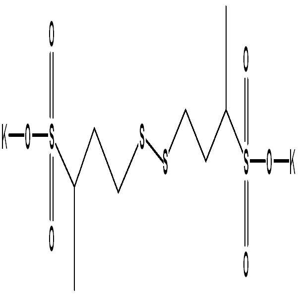
(K는 수소, 알킬 또는 금속)(K is hydrogen, alkyl or metal)
보다 상세하게, 상기 K는 수소, 리튬, 소디움 또는 칼륨(potassium)일 수 있다. 상기 [화학식 2]의 화합물은 이중황화(di-sulfide) 화합물로 이해될 수 있다. In more detail, K may be hydrogen, lithium, sodium, or potassium (potassium). The compound of [Formula 2] may be understood as a di-sulfide compound.
상기 제1 실시예에 의한 구리 도금 용액은 상기 제3 첨가제를 0.5 내지 200mg/L 정도를 함유할 수 있고, 보다 구체적으로, 약 1 내지 50mg/L 정도를 함유할 수 있다. 상기 제3 첨가제는 아래의 [화학식 3]으로 표현된 화합물을 포함할 수 있다.The copper plating solution according to the first embodiment may contain about 0.5 to 200 mg / L of the third additive, and more specifically, about 1 to 50 mg / L. The third additive may include a compound represented by the following [Formula 3].
[화학식 3](3)

(n은 평균 중합도, 예를 들어5~100, 특히 18)(n is the average degree of polymerization, for example 5-100, in particular 18)
상기 [화학식 3]의 화합물은 폴리에틸렌이민(polyethyleneimine) 화합물로 이해될 수 있다. 특히, 벤젠 고리를 가진 폴리에틸렌이민 화합물로 이해될 수 있다. 상기 Cl- 이온은 상기 화합물을 전기적 중성 상태로 유지시킬 수 있다.The compound of [Formula 3] may be understood as a polyethyleneimine compound. In particular, it can be understood as a polyethyleneimine compound having a benzene ring. The Cl − ions may keep the compound in an electrically neutral state.
제2 Second 실시예Example
본 발명의 기술적 사상의 제2 실시예에 의한 구리 도금 용액은 구리 공급원으로 메탄술폰산 구리(II), 전해물질로 메탄술폰산, 염소 이온원, 상기 제2 첨가제, 상기 제3 첨가제, 제4 첨가제 및 물을 함유할 수 있다. 상기 제1 실시예에 의한 구리 도금 용액의 상기 제1 첨가제가 상기 제4 첨가제로 교환된 경우로 이해될 수 있다. 상기 제4 첨가제는 폴리프로필렌 글리콜(polypropylene glycol, (CH2CH(OH)CHOH)n, n은 양의 정수)와 폴리에틸렌 산화물(polyethylene oxide, C2H4O)의 공중합체(co-polymer) 로 이해될 수 있다. 보다 상세하게, 약 90질량%의 폴리프로필렌 글리콜과 약 10질량%의 폴리에틸렌 산화물의 공중합체로 이해될 수 있다. 또는, 상기 공중합체는 평균 분자량 3800의 디올 화합물(diol compound)로 이해될 수 있다. 그 외, 함유량 등은 상기 제1 실시예에 의한 구리 도금 용액을 참조하여 이해될 수 있다.Copper plating solution according to a second embodiment of the present invention is a copper source of methanesulfonic acid (II), methanesulfonic acid as an electrolytic material, chlorine ion source, the second additive, the third additive, the fourth additive and It may contain water. It may be understood that the first additive of the copper plating solution according to the first embodiment is replaced with the fourth additive. The fourth additive is a copolymer of polypropylene glycol (CH 2 CH (OH) CHOH) n , n is a positive integer) and polyethylene oxide (C 2 H 4 O) It can be understood as. More specifically, it can be understood as a copolymer of about 90 mass% polypropylene glycol and about 10 mass% polyethylene oxide. Alternatively, the copolymer can be understood as a diol compound having an average molecular weight of 3800. In addition, the content and the like can be understood with reference to the copper plating solution according to the first embodiment.
제3실시예Third Embodiment
본 발명의 기술적 사상의 제3 실시예에 의한 구리 도금 용액은 구리 공급원으로 메탄술폰산 구리(II), 전해 물질로 메탄술폰산, 염소 이온원, 상기 제2 첨가제, 상기 제3 첨가제, 제5 첨가제 및 물을 함유할 수 있다. 상기 제1 실시예에 의한 구리 도금 용액의 상기 제1 첨가제 또는 상기 제2 실시예에 의한 상기 제4 첨가제가 상기 제5 첨가제로 교환된 경우로 이해될 수 있다. 보다 상세하게, 상기 제5 첨가제는 약 60질량%의 폴리프로필렌 글리콜과 약 40질량%의 폴리에틸렌 산화물의 공중합체로 이해될 수 있다. 또는, 상기 공중합체는 평균 분자량 4200의 디올 화합물로 이해될 수 있다. 그 외, 함유량 등은 상기 제1 실시예에 의한 구리 도금 용액을 참조하여 이해될 수 있다.Copper plating solution according to a third embodiment of the present invention is a copper source of methanesulfonic acid (II), methanesulfonic acid as an electrolytic material, chlorine ion source, the second additive, the third additive, the fifth additive and It may contain water. It may be understood that the first additive of the copper plating solution according to the first embodiment or the fourth additive according to the second embodiment is replaced with the fifth additive. More specifically, the fifth additive may be understood as a copolymer of about 60 mass% polypropylene glycol and about 40 mass% polyethylene oxide. Alternatively, the copolymer can be understood as a diol compound having an average molecular weight of 4200. In addition, the content and the like can be understood with reference to the copper plating solution according to the first embodiment.
제4실시예Fourth Embodiment
본 발명의 기술적 사상의 제4 실시예에 의한 구리 도금 용액은 구리 공급원으로 메탄술폰산 구리(II), 전해 물질로 메탄술폰산, 염소 이온원, 상기 제2 첨가제, 상기 제3 첨가제, 제6 첨가제 및 물을 함유할 수 있다. 상기 제1 실시예에 의한 구리 도금 용액의 상기 제1 첨가제, 상기 제2 실시예에 의한 구리 도금 용액의 상기 제4 첨가제, 또는 상기 제3 실시예에 의한 구리 도금 용액의 상기 제5 첨가제가 상기 제6 첨가제로 교환된 경우로 이해될 수 있다.Copper plating solution according to a fourth embodiment of the present invention is copper methanesulfonic acid (II) as the copper source, methanesulfonic acid as the electrolytic material, chlorine ion source, the second additive, the third additive, the sixth additive and It may contain water. The first additive of the copper plating solution according to the first embodiment, the fourth additive of the copper plating solution according to the second embodiment, or the fifth additive of the copper plating solution according to the third embodiment is It can be understood as being exchanged with the sixth additive.
상기 제6 첨가제는 하기 [화학식 4]로 표현될 수 있다.The sixth additive may be represented by the following [Formula 4].
![]()
![]()
(p는 평균 중합도, 예를 들어 9)(p is the average degree of polymerization, for example 9)
R은 예를 들어, 다음 [화학식 5] 또는 [화학식 6]으로 표현되는 화합물들 중 어느 하나 또는 둘의 조합일 수 있다.R may be, for example, any one or a combination of the compounds represented by the following [Formula 5] or [Formula 6].
[화학식 5][Chemical Formula 5]

상기 [화학식 5]의 화합물은 탄소수 11의 1급 지방족 알코올로 이해될 수 있다.The compound of Formula 5 may be understood as a primary aliphatic alcohol having 11 carbon atoms.
[화학식 6][Formula 6]
![]()
![]()
상기 [화학식 6]의 화합물은 탄소수 11의 2급 지방족 알코올로 이해될 수 있다. The compound of Formula 6 may be understood as a secondary aliphatic alcohol having 11 carbon atoms.
따라서, 상기 제6 첨가제는 탄소수 11의 1급 지방족 알코올에 산화 에틸렌을 부가한 화합물 및 탄소수 11의 2급 지방족 알코올에 산화 에틸렌을 부가한 디올 화합물로 이해될 수 있다. 보다 상세하게, 상기 제6 첨가제는 탄소수 11의 1급 지방족 알코올과 탄소수 11의 2급 지방족 알코올의 1:1 혼합물에 산화 에틸렌을 약 10질량%로 함유하는 디올 화합물로 이해될 수 있다. 상기 탄소수 11의 1급 지방족 알코올과 상기 탄소수 11의 2급 지방족 알코올은 질량비로 혼합될 수 있다. 그 외, 함유량 등은 상기 제1 실시예에 의한 구리 도금 용액을 참조하여 이해될 수 있다.Therefore, the sixth additive may be understood as a compound in which ethylene oxide is added to a primary aliphatic alcohol having 11 carbon atoms and a diol compound in which ethylene oxide is added to a secondary aliphatic alcohol having 11 carbon atoms. More specifically, the sixth additive may be understood as a diol compound containing about 10 mass% of ethylene oxide in a 1: 1 mixture of a C 11 primary aliphatic alcohol and a C 11 secondary aliphatic alcohol. The primary aliphatic alcohol having 11 carbon atoms and the secondary aliphatic alcohol having 11 carbon atoms may be mixed in a mass ratio. In addition, the content and the like can be understood with reference to the copper plating solution according to the first embodiment.
제5실시예Fifth Embodiment
본 발명의 기술적 사상의 제5 실시예에 의한 구리 도금 용액은 구리 공급원으로 메탄술폰산 구리(II), 전해 물질로 메탄술폰산, 염소 이온원, 상기 제1 첨가제, 상기 제2 첨가제, 제7 첨가제 및 물을 함유할 수 있다. 상기 제1 실시예에 의한 구리 도금 용액의 상기 제3 첨가제가 상기 제7 첨가제로 교환된 경우로 이해될 수 있다. Copper plating solution according to a fifth embodiment of the present invention of the present invention is copper methanesulfonic acid (II) as a copper source, methanesulfonic acid as the electrolytic material, chlorine ion source, the first additive, the second additive, the seventh additive and It may contain water. It may be understood that the third additive of the copper plating solution according to the first embodiment is replaced with the seventh additive.
상기 제7 첨가제는 하기 [화학식 7]로 표현될 수 있다.The seventh additive may be represented by the following [Formula 7].
[화학식 7][Formula 7]

(a는 수평균 분자량이 30000이 되는 수, M은 알칼리 금속, 예를 들어 칼륨(potassium))(a is a number having a number average molecular weight of 30000, M is an alkali metal, for example potassium)
상기 제7 첨가제는 상기 제3 첨가제와 비교하여, 벤젠 고리대신 술폰산염을 가진 폴리에틸렌으로 치환된 폴리에틸렌이민 화합물로 이해될 수 있다. 그 외, 함유량 등은 상기 제1 실시예에 의한 구리 도금 용액을 참조하여 이해될 수 있다.The seventh additive may be understood as a polyethyleneimine compound substituted with polyethylene having a sulfonate instead of a benzene ring as compared to the third additive. In addition, the content and the like can be understood with reference to the copper plating solution according to the first embodiment.
제6 6th 실시예Example
본 발명의 기술적 사상의 제6 실시예에 의한 구리 도금 용액은 구리 공급원으로 메탄술폰산 구리(II), 전해 물질로 메탄술폰산, 염소 이온원, 상기 제1 첨가제, 상기 제2 첨가제, 제8 첨가제 및 물을 함유할 수 있다. 상기 제1 실시예에 의한 구리 도금 용액의 상기 제3 첨가제 또는 상기 제5 실시예에 의한 구리 도금 용액의 상기 제7 첨가제가 상기 제8 첨가제로 교환된 경우로 이해될 수 있다.The copper plating solution according to the sixth embodiment of the inventive concept is copper methanesulfonic acid (II) as the copper source, methanesulfonic acid as the electrolytic material, chlorine ion source, the first additive, the second additive, the eighth additive and It may contain water. It may be understood that the third additive of the copper plating solution according to the first embodiment or the seventh additive of the copper plating solution according to the fifth embodiment is replaced with the eighth additive.
상기 제8 첨가제는 하기 [화학식 8]로 표현될 수 있다.The eighth additive may be represented by the following [Formula 8].
[화학식 8][Formula 8]
(b는 수평균 분자량이 70000이 되는 수, X-는 취소 분자이고, 예를 들어 Cl-)(b has a number average molecular weight of a number of 70000, X - is a clear molecule, such as Cl -)
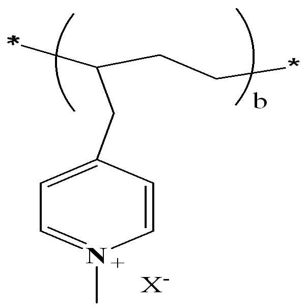
상기 제8 첨가제는 4급화 poly(2-vinylpyridian) 화합물로 이해될 수 있다. 그 외, 함유량 등은 상기 제1 실시예에 의한 구리 도금 용액을 참조하여 이해될 수 있다. 상기 취소 분자는 상기 단량체(monomer)를 전기적 중성 상태로 유지시킬 수 있다.The eighth additive may be understood as a quaternized poly (2-vinylpyridian) compound. In addition, the content and the like can be understood with reference to the copper plating solution according to the first embodiment. The cancellation molecule may keep the monomer in an electrically neutral state.
제7 7th 실시예Example
본 발명의 기술적 사상의 제7 실시예에 의한 구리 도금 용액은 구리 공급원으로 메탄술폰산 구리(II), 전해 물질로 메탄술폰산, 염소 이온원, 상기 제1 첨가제, 상기 제2 첨가제, 제9 첨가제 및 물을 함유할 수 있다. 상기 제1 실시예에 의한 구리 도금 용액의 상기 제3 첨가제, 상기 제5 실시예에 의한 구리 도금 용액의 상기 제7 첨가제, 또는 상기 제6 실시예에 의한 상기 제8 첨가제가 상기 제9 첨가제로 교환된 경우로 이해될 수 있다.Copper plating solution according to a seventh embodiment of the present invention is a copper source of methanesulfonic acid (II), an electrolytic material of methanesulfonic acid, chlorine ion source, the first additive, the second additive, the ninth additive and It may contain water. The third additive of the copper plating solution according to the first embodiment, the seventh additive of the copper plating solution according to the fifth embodiment, or the eighth additive according to the sixth embodiment is referred to as the ninth additive. It can be understood as an exchange case.
상기 제9 첨가제는 하기 [화학식 9]로 표현될 수 있다.The ninth additive may be represented by the following [Formula 9].
[화학식 9][Chemical Formula 9]

(c는 수평균 분자량이 60000이 되는 수)(c is a number of which the number average molecular weight is 60000)
상기 제9 첨가제는 poly(2-vinylpyridian) 화합물로 이해될 수 있다. 그 외, 함유량 등은 상기 제1 실시예에 의한 구리 도금 용액을 참조하여 이해될 수 있다.The ninth additive may be understood as a poly (2-vinylpyridian) compound. In addition, the content and the like can be understood with reference to the copper plating solution according to the first embodiment.
제8 8th 실시예Example
본 발명의 기술적 사상의 제8 실시예에 의한 구리 도금 용액은 메탄술폰산 구리(II), 메탄술폰산, 염소 이온원, 상기 제1 첨가제, 상기 제2 첨가제, 제10 첨가제 및 물을 함유할 수 있다. 상기 제1 실시예에 의한 구리 도금 용액의 상기 제3 첨가제, 상기 제5 실시예에 의한 구리 도금 용액의 상기 제7 첨가제, 상기 제6 실시예에 의한 상기 제8 첨가제, 또는 상기 제7 실시예에 의한 구리 도금 용액의 상기 제9 첨가제가 상기 제10 첨가제로 교환된 경우로 이해될 수 있다.The copper plating solution according to the eighth embodiment of the inventive concept may contain copper methanesulfonic acid (II), methanesulfonic acid, a chlorine ion source, the first additive, the second additive, the tenth additive, and water. . The third additive of the copper plating solution according to the first embodiment, the seventh additive of the copper plating solution according to the fifth embodiment, the eighth additive according to the sixth embodiment, or the seventh embodiment It can be understood as the case where the ninth additive of the copper plating solution by is replaced with the tenth additive.
상기 제10 첨가제는 하기 [화학식 10]로 표현될 수 있다.The tenth additive may be represented by the following [Formula 10].
[화학식 10][Formula 10]

(x, y는 수평균 분자량이 40000이 되는 수, x : y는 약 5 : 9.5)(x, y is the number of which the number average molecular weight is 40000, x: y is about 5: 9.5)
상기 제10 첨가제는 비닐피롤리돈(vinylpyrrolidone)과 염화 메틸비닐 이미다조리움(methylvinyl imidazolium chloride)의 공중합체로 이해될 수 있다. 그 외, 함유량 등은 상기 제1 실시예에 의한 구리 도금 용액을 참조하여 이해될 수 있다.The tenth additive may be understood as a copolymer of vinylpyrrolidone and methylvinyl imidazolium chloride. In addition, the content and the like can be understood with reference to the copper plating solution according to the first embodiment.
부가하여, 상기 본 발명의 제1 내지 제8 실시예들에 의한 구리 도금 용액들은 계면활성제, 소포제(anti-foamer), 및/또는 연성화제(ductilizer)를 더 포함할 수 있다. 상기 본 발명의 제1 내지 제8 실시예들에 의한 구리 도금 용액들은 상기 계면활성제로 예를 들어, 폴리옥시에틸렌알킬에테르 (R-O(CH2CH2O)mH, R은 알킬, m은 양의 정수), 다양한 지방산 솔비탄에스테르들, 지방산 디에탄올아민 (R-CON(CH2CH2OH)2, R은 알킬), 또는 알킬모노글리세릴에테르 (R-OCH2CH(OH)CH2OH, R은 알킬) 등의 알킬글리콜, 폴리에틸렌 글리콜 폴리머, 또는 폴리비닐 알코올 폴리머 등을 약 0.05 내지 10mg/L 정도로 포함할 수 있다. 이 외에, 알려진 다양한 소포제 및/또는 연성화제를 포함할 수 있다.In addition, the copper plating solutions according to the first to eighth embodiments of the present invention may further include a surfactant, an anti-foamer, and / or a ductilizer. The copper plating solutions according to the first to eighth embodiments of the present invention are used as the surfactant, for example, polyoxyethylene alkyl ether (RO (CH 2 CH 2 O) m H, R is alkyl, m is the amount Integer), various fatty acid sorbitan esters, fatty acid diethanolamine (R-CON (CH 2 CH 2 OH) 2 , R is alkyl), or alkyl monoglyceryl ether (R-OCH 2 CH (OH) CH 2 OH, R may include alkyl glycols such as alkyl), polyethylene glycol polymers, or polyvinyl alcohol polymers, and the like, about 0.05 to 10 mg / L. In addition, various known antifoaming agents and / or softeners may be included.
상기 구리 도금 용액은 수용액 또는 분산액의 형태로 제공될 수 있다.The copper plating solution may be provided in the form of an aqueous solution or a dispersion.
상기 구리 도금 용액은 베이스 용액에 상기 제1 내지 제 10 첨가제들을 첨가하여 제조될 수 있다. 상기 제1 내지 제10 첨가제들은 각각의 수용액 형태 또는 첨가제들이 선택적으로 또는 모두가 배합된 수용액 형태로 첨가될 수도 있다.The copper plating solution may be prepared by adding the first to tenth additives to the base solution. The first to tenth additives may be added in the form of an aqueous solution in which each aqueous solution or additives are selectively or all combined.
상기 베이스 용액은 물, 상기 메탄술폰산 구리(II), 상기 메탄술폰산, 및 상기 염소 이온원을 포함할 수 있다.The base solution may include water, the copper methanesulfonic acid (II), the methanesulfonic acid, and the chlorine ion source.
상기 메탄술폰산 구리(II)는 무수화물 상태로 제공되어 상기 베이스 용액에 배합될 수 있다. 상기 메탄술폰산 구리(II)가 황산구리로 교환된 경우, 황산 구리는 수화물 형태, 특히 오수화물(CuSO4:5H2O) 상태로 제공되어 상기 베이스 용액에 배합될 수 있다The copper methanesulfonic acid (II) may be provided in an anhydride state and blended into the base solution. When the copper methanesulfonic acid (II) is exchanged for copper sulfate, copper sulfate may be provided in the form of a hydrate, in particular in the form of pentahydrate (CuSO 4 : 5H 2 O), to be incorporated into the base solution.
상기 메탄술폰산 또는 황산 및/또는 상기 염소 이온원은 각각 독립적으로 제공되어 상기 베이스 용액에 배합될 수 있다.The methanesulfonic acid or sulfuric acid and / or the chlorine ion source may be provided independently of each other and combined in the base solution.
이어서, 상기 제1 내지 제8 실시예들에 의한 구리 도금 용액을 사용하여 구리 도금 공정을 수행하는 것과 본 발명의 기술적 사상에 의한 구리 도금 장치가 설명된다. 본 명세서에서, 구리 도금 공정은 특히 반도체 제조 공정에서 TSV (through silicon via) 플러그를 형성하는 공정이 예시적으로 설명된다.Next, a copper plating process using the copper plating solutions according to the first to eighth embodiments and a copper plating apparatus according to the spirit of the present invention will be described. In the present specification, a copper plating process is exemplarily described as a process of forming a through silicon via (TSV) plug, particularly in a semiconductor manufacturing process.
도 1은 본 발명의 기술적 사상에 의한 구리 도금 장치를 개략적으로 도시한 도면이다.1 is a view schematically showing a copper plating apparatus according to the spirit of the present invention.
도 1을 참조하면, 본 발명의 기술적 사상에 의한 구리 도금 장치(10)는, 도금 파트(12A) 및 공급 파트(12B)를 포함할 수 있다. 상기 도금 파트(12A)는 도금 용기(14), 공급구(16A), 순환구(16B), 캐소드 전극(18), 애노드 전극(20), 회전 모터(22) 및 바이어스 전원(24)을 포함할 수 있다. 상기 공급구(16A)를 통하여 구리 도금 용액(50)이 공급될 수 있다. 상기 순환구(16B)는 상기 도금 용기(14) 내에 채워진 상기 구리 도금 용액(50)을 상기 공급 파트(12B)로 전달, 순환시키기 위하여 이용된다. 상기 캐소드 전극(18) 상에 웨이퍼(W)가 고정(hold)될 수 있다. 상기 캐소드 전극(18)은 상기 회전 모터(22)에 의해 구동, 회전될 수 있다. 상기 캐소드 전극(18)과 애노드 전극(20)의 사이에는 멤브레인(23)이 설치될 수 있다. 상기 멤브레인(23)은 상기 공급구(16A)로 공급되는 상기 구리 도금 용액(50)을 상기 웨이퍼(W) 상으로 분산시켜 공급하는 기능을 가질 수 있다. 다른 말로, 상기 구리 도금 용액(50) 내에 포함된 여러 구성 요소들의 농도를 균일화 시킬 수 있다.Referring to FIG. 1, the
상기 공급 파트(12B)는 보조 저장 용기(28), 용액 순환로(26, circulating path), 및 다수 개의 단위 공급 용기들(38)을 포함할 수 있다.The
상기 용액 순환로(26)는 상기 순환구(16B) 통해 상기 구리 도금 용액(50)을 전달받아 상기 보조 저장 용기(28)로 전달할 수 있다. 상기 용액 순환로(26)는 상기 구리 도금 용액(50)을 순환시키기 위한 순환 펌프(30) 및 상기 구리 도금 용액(50)을 여과하기 위한 필터(32)를 포함할 수 있다.The
상기 용액 순환로(26)는 상기 보조 저장 용기(28)로부터 재배합(re-blend)된 구리 도금 용액(50a)을 상기 도금 용기(14)로 전달하기 위한 공급 펌프(34) 및 액체 유량 조절부(36, liquid flow meter)를 포함할 수 있다.The
상기 단위 공급 용기들(38)은 상기 보조 저장 용기(28)로 상기 재배합된 구리 도금 용액(50a)의 구성 요소들을 각각 독립적 또는 배합물을 공급할 수 있다. 예를 들어, 하나의 구성 요소를 수용액 형태로 제공할 수도 있고, 둘 이상의 구성 요소가 배합된 수용액을 제공할 수도 있다. 상기 단위 공급 용기들(38)로부터 상기 보조 저장 용기(28)로 제공되는 구성 요소들의 유량은은 단위 액체 유량 조절부들(42, unit liquid flow meters)에 의해 조절될 수 있고, 각 단위 액체 유량 조절부들(42)은 제어부(40, control unit)에 의해 제어될 수 있다.The
상기 보조 저장 용기(28)에는 모니터링부(44, monitoring unit)이 설치될 수 있다. 상기 모니터링부(44)는 상기 보조 저장 용기 내의 재배합된 구리 도금 용액(50a)의 일부를 샘플링하여 구리 도금 공정을 수행하기에 적절한 상태인지 모니터링할 수 있다. 이에 의해 생성된 모니터링 정보는 상기 제어부(40)로 전달될 수 있고, 상기 제어부(40)는 상기 모니터링 정보에 의해 각 단위 액체 유량 조절부들(42)을 제어할 수 있다.A
상기 보조 저장 용기(28)에는 배출 밸브(45)를 가진 배출구(46)가 더 설치될 수 있다.The
상기 공급 파트(12B)는 구리 도금 공정을 수행하는 동안, 상기 도금 용기(14) 내의 구리 도금 용액(50)을 순환시켜 상기 구리 도금 용액(50)을 교환, 정화, 보충, 재생 또는 기타 다양한 목적을 달성하는데 이용될 수 있다.The
이어서, 본 발명의 기술적 사상들에 의한 구리 도금 용액들 및 상기 구리 도금 장치(10)를 이용하여 구리 도금 공정을 수행하는 것이 설명된다.Next, it will be described to perform a copper plating process using the copper plating solutions and the
도 2a는 본 발명의 기술적 사상이 적용될 수 있는 TSV 플러그를 형성하기 전의 웨이퍼(W)의 개략적인 평면도이고 도 2b는 도 2a의 CA 영역의 개략적인 확대도이다.FIG. 2A is a schematic plan view of a wafer W before forming a TSV plug to which the inventive concept may be applied, and FIG. 2B is a schematic enlarged view of a CA region of FIG. 2A.
도 2a는 TSV 플러그를 형성하기 전의 웨이퍼(W)의 개략적인 평면도이고 도 2b는 도 2a의 CA 영역의 개략적인 확대도이다. FIG. 2A is a schematic plan view of the wafer W before forming the TSV plug and FIG. 2B is a schematic enlarged view of the CA region of FIG. 2A.
도 2a를 참조하면, 상기 웨이퍼(W) 상에 수 십 내지 수 백 개의 반도체 칩(C)들이 섬 형태로 배열된다. 상기 각 반도체 칩(C)들의 사이에는 스크라이브 레인들(SL, scribe lane)이 배열된다. 상기 웨이퍼(W)는 플랫 존(flat zone) 타입과 노치(notch) 타입이 있으며, 본 도면에는 예시적으로 플랫 존 타입의 웨이퍼(W)가 도시되었다. 상기 반도체 칩들(C)도 다양한 모양으로 형성될 수 있는데, 본 도면에서는 예시적으로 정사각형 모양으로 형성된 것으로 가정하여 도시되었다.Referring to FIG. 2A, tens to hundreds of semiconductor chips C are arranged in an island shape on the wafer W. Referring to FIG. A scribe lane SL is arranged between the semiconductor chips C. FIG. The wafer W has a flat zone type and a notch type, and the wafer W of the flat zone type is exemplarily illustrated in the drawing. The semiconductor chips C may also be formed in various shapes. In the drawing, the semiconductor chips C are exemplarily illustrated as having a square shape.
도 2b를 참조하면, 상기 반도체 칩(C)은 다수개의 입출력 패드들 (P, I/O pads)을 포함한다. 본 실시예에서는 예시적으로 상기 입출력 패드들(P)이 상기 반도체 칩(C)의 중앙에 두 줄로 배열된 경우가 예시된다. 본 실시예에서는, 본 발명의 기술적 사상이 쉽게 이해되도록 설명하기 위하여, 특히 TSV 플러그가 상기 입출력 패드들(P)과 수직으로 정렬되도록 형성된 경우가 예시된다. 예시된 것과 달리, 상기 입출력 패드들(P)은 상기 반도체 칩(C)의 외곽을 따라 배열될 수도 있고 다양한 배열로 조합될 수 있다.Referring to FIG. 2B, the semiconductor chip C includes a plurality of input / output pads P and I / O pads. In the present exemplary embodiment, a case where the input / output pads P are arranged in two rows in the center of the semiconductor chip C is illustrated. In the present embodiment, in order to easily understand the technical spirit of the present invention, a case in which the TSV plug is formed to be vertically aligned with the input / output pads P is illustrated. Unlike the illustrated example, the input / output pads P may be arranged along the periphery of the semiconductor chip C or may be combined in various arrangements.
도 3a 내지 3h는 구리 도금 공정을 설명하는 도 2b의 I-I'의 종단면도들이다. 도 1과 비교하여, 상기 웨이퍼(W)의 상하가 반전된 것으로 이해될 수 있다.3A-3H are longitudinal cross-sectional views of II ′ of FIG. 2B illustrating the copper plating process. Compared with FIG. 1, it can be understood that the top and bottom of the wafer W are reversed.
도 3a를 참조하면, 웨이퍼 상태의 기판(110)의 상면에 보호층(120)이 형성되고, 비아 홀, 예를 들어 TSV 홀을 형성하기 위한 제1 개구부들(H1)을 가진 마스크 패턴(130)이 형성될 수 있다. 상기 보호층(120)은 실리콘 산화막 또는 실리콘 질화막을 포함할 수 있다. 상기 마스크 패턴(130)은 폴리이미드, 포토레지스트 같은 유기 고분자 수지, 또는 무기 수지를 포함할 수 있다.Referring to FIG. 3A, a
도 3b를 참조하면, 상기 마스크 패턴(130)을 식각 마스크로 사용하는 식각 공정을 수행하여 상기 기판(110)의 일정 깊이까지 TSV 홀들(H2)이 형성될 수 있다. 상기 TSV홀들(H2)은 상기 기판(110)을 관통하지 않고 일정 깊이까지만 형성될 수 있다. Referring to FIG. 3B, TSV holes H2 may be formed to a predetermined depth of the
도 3c를 참조하면, 상기 마스크 패턴(130)이 제거될 수 있다. 이 공정에서, 상기 보호층(120)의 표면이 노출될 수 있다.Referring to FIG. 3C, the
도 3d를 참조하면, 상기 보호층(120) 및 상기 TSV 홀들(H2)의 표면들 상에 배리어 층(140) 및 씨드 층(150)이 형성될 수 있다. 상기 배리어 층(140)은 탄탈룸(Ta) 또는 티타늄/티타늄 질화막 (Ti/TiN)을 포함할 수 있다. 본 실시예에서는 예시적으로 탄탈룸이 이용될 수 있다. 상기 씨드 층(150)은 구리를 포함할 수 있다. 상기 배리어 층(140) 및 상기 씨드 층(150)은 물리 기상 증착 (PVD) 공정을 통해 형성될 수 있다.Referring to FIG. 3D, a
도 1 및 3e를 참조하면, 본 발명의 실시예들에 의한 구리 도금 용액(50)들을 사용하는 구리 도금 공정을 수행하여, 상기 기판(110)의 표면 부위 및 상기 TSV홀들(H2)내부를 채우는 제1 구리 도금층(160a)이 형성될 수 있다. 이 공정은 도 1을 더 참조하여 이해될 수 있다. 이 공정은, 상기 제1 실시예에 의한 구리 도금 용액(50)을 사용하여 수행되는 것이 설명된다. 도 1의 웨이퍼(W)는 도 3e의 기판(110)으로 이해될 수 있다.1 and 3E, a copper plating process using copper plating solutions 50 according to embodiments of the present invention is performed to fill a surface portion of the
본 실시예에 의한 구리 도금 공정의 공정 조건들은 예를 들어, 다음과 같은 범위 내에서 수행될 수 있다.Process conditions of the copper plating process according to the present embodiment may be performed, for example, within the following range.
상기 기판(110)이 상기 캐소드 전극(18) 상에 장착되고, 상기 구리 도금 용액(50) 내에 침지될 수 있다. 이때, 침지되기 직전에 상기 회전 모터(22)에 의해 상기 기판(110)이 예를 들어, 약 400 내지 3000RPM(rotation per a minute) 정도로 고속으로 회전되어 표면의 이물질 등이 제거될 수 있다.The
상기 기판(110)이 상기 구리 도금 용액(50) 내에 침지된 후, 상기 기판의 온도 및/또는 구리 도금 용액(50)의 온도는 약 15 내지 60℃ 범위로 유지될 수 있고, 바람직하게는 약 20 내지 40℃ 범위로 유지될 수 있다.After the
상기 캐소드(18)와 애노드(20) 사이에 인가되는 전류 밀도는 약 0.1~200㎃/㎠ 범위로 유지될 수 있다. 특히, 상기 TSV 홀들(H3)의 내부를 채우는 구리 도금 공정은 예를 들어, 약 0.1~100㎃/㎠ 정도의 상대적으로 낮은 전류 밀도 범위에서 수행될 수 있고, 상기 기판(110)의 표면에 구리 도금층을 형성하기 위한 구리 도금 공정은 예를 들어 1~300㎃/㎠ 정도의 상대적으로 높은 전류 밀도 범위에서 수행될 수 있다. 즉, 비아 홀을 채우는 도금 공정에서는 전류 밀도가 상대적으로 낮아질 수 있다.The current density applied between the
상기 기판(110)은 구리 도금 공정이 수행되는 동안, 상기 구리 도금 용액(50) 내에서 6 내지 60RPM으로 회전될 수 있다.The
상기 구리 도금 용액(50)은 상기 공급구(16A) 및 상기 순환부(16B)를 통해 0.1 내지 300LPM(liter per minute)의 순환량을 유지할 수 있고, 예를 들어 5 내지 30LPM의 흐름을 유지할 수 있다.The copper plating solution 50 may maintain a circulation amount of 0.1 to 300 liters per minute (LPM) through the
본 실시예에 의한 구리 도금 공정은 다음과 같은 공정 조건 하에서 실험적으로 수행되었다. 먼저, 상기 TSV홀(H2) 내에 물을 채운 후, 상기 구리 도금 용액(50) 내에 약 2분간 침지하였다. 이후, 상기 구리 도금 용액(50)의 온도를 약 25℃로 유지하고, 하기 표 1에 제시된 전류 밀도 및 공정 시간으로 총 38분간 상기 구리 도금 공정이 수행되었다. Copper plating process according to the present embodiment was carried out experimentally under the following process conditions. First, after filling water in the TSV hole (H2), it was immersed in the copper plating solution 50 for about 2 minutes. Thereafter, the temperature of the copper plating solution 50 was maintained at about 25 ° C., and the copper plating process was performed for a total of 38 minutes at the current density and process time shown in Table 1 below.
본 도금 공정은 상기 TSV 홀(H2)을 구리 도금하기 위한 공정이므로 공정 진행에 따라 전류 밀도를 상승시키며 실험되었다. 예를 들어, 상기 TSV 홀(H2)의 깊은 부분에 구리 도금층을 형성하기 위한 단계에서는 상대적으로 낮은 전류밀도를 유지하고, 상기 TSV 홀(H2)이 점차 얕아질수록 전류밀도가 높아진다는 것을 의미한다.Since the plating process is a process for copper plating the TSV hole (H2), it was tested by increasing the current density as the process proceeds. For example, in the step of forming a copper plating layer in the deep portion of the TSV hole H2, the current density is relatively low, and as the TSV hole H2 becomes shallower, it means that the current density becomes higher. .
상기 구리 도금 용액(50)은 구리 이온들(Cu2 +), 수소 이온들(H+), 염소 이온들(Cl-), 억제제(S), 촉진제(A), 및 평활제(L)를 포함한다. 도면에서, 메탄술폰산과 염소 이온이 생략되었다. 상기 억제제(S)는 앞서 예시된 제1 첨가제 또는 제4 내지 제6 첨가제들 중 하나 일 수 있다. 상기 촉진제(A)는 앞서 예시된 제2 첨가제일 수 있다. 상기 평활제(L)는 앞서 예시된 제3 첨가제, 또는 제7 내지 제10 첨가제들 중 하나일 수 있다. 앞서 언급되었듯이, 상기 억제제(S)가 상기 제1 첨가제이고, 상기 촉진제(A)가 상기 제2 첨가제이고, 상기 평활제(L)가 상기 제3 첨가제인 경우가 설명된다. 상기 억제제(S), 촉진제(A), 및 평활제(L)들의 작용이 설명된다. 본 발명의 실시예에 따른 도금 용액들의 성능을 보다 더 우수하게 할 수 있는 예시적인 구리 도금 공정을 통해 설명된다.Said copper plating solution (50) is a copper ion (Cu 2 +), hydrogen ions (H +), chlorine ions (Cl -), the inhibitor (S), accelerator (A), and a slip agent (L) Include. In the figure, methanesulfonic acid and chlorine ions are omitted. The inhibitor (S) may be one of the first or fourth to sixth additives exemplified above. The accelerator (A) may be the second additive illustrated above. The leveling agent (L) may be one of the third additives or the seventh to tenth additives exemplified above. As mentioned above, the case where the inhibitor (S) is the first additive, the accelerator (A) is the second additive, and the leveling agent (L) is the third additive is described. The action of the inhibitors (S), promoters (A), and levelers (L) is described. This is illustrated through an exemplary copper plating process that can further improve the performance of plating solutions according to embodiments of the present invention.
상기 억제제(S)의 (폴리)에테르(-H2C2-O-C2H4O-)는 상기 씨드 층(150) 또는 상기 제1 구리 도금층(160a)의 습윤(wetting) 특성을 개선시킬 수 있다. 상기 구리 도금 용액(50)에 함유된 상기 억제제(S)의 함유량이 너무 적으면 도금 속도를 제어할 수 없어서 씸(seam) 또는 보이드(void)가 발생하는 것을 억제하기 어렵고, 너무 많으면 도금 속도가 저하되어 생산성이 낮아질 수 있다. 즉, 상기 억제제(S)는 습윤제 및 억제제의 기능을 수행할 수 있다. 실험적으로, 상기 구리 도금 용액(50)이 상기 억제제(S)를 약 0.5 내지 200mg/L로 함유하면 본 발명의 목적을 달성할 수 있었고, 특히 1 내지 50mg/L 로 함유하면 보다 적절한 실험 결과를 얻을 수 있었다. 본 실험에 사용된 상기 구리 도금 용액(50)은 상기 억제제(S)를 2.86mg/L로 함유할 수 있다. 또한, 상기 억제제(S)의 분자량이 커질 경우, 도금 속도가 과하게 억제되어 평활 효과가 저하되었고, 반대로 분자량이 너무 작은 경우 도금 억제 효과가 저하되었다. 따라서, 상기 억제제(S)의 분자량을 적절히 조절하기 위하여, 평균 중합도를 6 내지 14 범위 내에서 중합하였으며, 본 실험에서는 예시적으로 평균 중합도를 그 중간치인 10으로 중합한 화합물이 사용되었다.The (poly) ether (-H 2 C 2 -OC 2 H 4 O-) of the inhibitor (S) may improve the wetting properties of the
상기 촉진제(A)는 단일 황화물(mono sulfide compound)로 분리된 후, 반응기(K)가 구리 이온(Cu2 +)와 결합하여 2가 이온을 1가 이온화함으로써, 낮은 에너지에서도 구리 도금 공정이 잘 수행될 수 있도록 구리 도금 반응을 촉진시킬 수 있다. 즉, 상기 구리 도금 용액(50)의 상기 촉진제(A)는 도금 촉진제로 작용할 수 있다. 따라서, 상기 구리 도금 용액(50)에 함유된 상기 촉진제(A)의 함유량이 적어지면 도금 속도가 낮아져 생산성이 저하되고 너무 많아지면 도금 속도를 제어하기 어려워질 수 있다. 도 3e에서, 상기 보호층(120)의 위쪽에는 상대적으로 상기 촉진제(A)가 상기 억제제(S)보다 적게 존재하고, 상기 TSV 홀(H2) 내에는 상대적으로 상기 촉진제(A)가 상기 억제제(S)보다 많이 존재할 수 있다. 따라서, 상기 TSV 홀(H2) 내부의 구리 도금 속도가 상기 보호층(120)의 위쪽보다 빠를 수 있다. 이에 의해, 상기 보호층(120)의 위쪽에 형성되는 구리 도금층의 두께(t1)보다 상기 TSV 홀(H2)의 바닥면에 형성되는 구리 도금층의 두께(t2)가 더 빠르고 두껍게 형성될 수 있다. 실험적으로, 상기 구리 도금 용액(50)이 상기 촉진제(A)를 약 10 내지 400mg/L 정도 함유하면 본 발명의 목적을 달성할 수 있었고, 특히 약 15 내지 200mg/L 함유하면 보다 적절한 실험 결과를 얻을 수 있었다. 상기 구리 도금 용액(50)을 사용하여 구리 도금 공정을 실험한 결과, 상기 촉진제(A)가 약 10mg/L 미만인 경우, 도금 속도가 현저히 저하되는 것을 알 수 있었다. 또한 상기 촉진제(A)가 약 400mg/L 을 초과하면 도금 속도 상승 효과가 포화되는 양상을 보이며, 또 상기 구리 도금 용액(50)의 수명을 단축할 우려가 있다. 본 실험에 사용된 상기 구리 도금 용액(50)은 촉진제(A)를 40.8mg/L로 함유할 수 있다.The accelerator (A) is well two days sulfide (mono sulfide compound) after the separation by the reactor (K) is a copper ion (Cu 2 +) and combined to divalent ions by monovalent ionization, copper even at a low energy coating process It can promote the copper plating reaction to be carried out. That is, the accelerator (A) of the copper plating solution 50 may act as a plating promoter. Therefore, when the content of the accelerator (A) contained in the copper plating solution 50 decreases, the plating rate may be lowered, and productivity may decrease, and when the content is too high, it may be difficult to control the plating rate. In FIG. 3E, the accelerator (A) is relatively less than the inhibitor (S) above the
상기 평활제(L)는 물에 녹아 질소 이온(N+)을 배출할 수 있다. 도면에서, 상기 평활제(L)는 N+이온을 의미할 수 있다. 상기 평활제(L)는 (-) 전계 방향, 즉 도 1의 웨이퍼(W)쪽으로 이동하여 상기 기판(110)의 표면 부위, 돌출 부위, 패턴의 밀도가 낮은 부위 및/또는 TSV 홀(H2)의 입구 부위에 집중될 수 있다. 이 부위는 구리 도금층이 형성되면서 전계가 집중되는 부위들이다. 상기 평활제(L)가 집중된 부위는 구리 도금 속도가 그렇지 않은 부분보다 느려진다. 따라서, 상기 평활제(L)들에 의해 구리 도금층이 전체적으로 비슷한 높이로 성장할 수 있다. 따라서, 상기 구리 도금 용액(50)에 함유된 상기 평활제(L)의 함유량이 적거나 중합도가 낮으면 도금된 구리 도금층의 평탄성이 매우 나빠질 것이고, 너무 많거나 중합도가 높으면 도금 속도를 심각하게 저하시킬 것이다. 실험적으로, 상기 구리 도금 용액(50)이 상기 평활제(L)를 약 0.5 내지 200mg/L을 포함하면 본 발명의 목적을 달성할 수 있었고, 특히 약 1 내지 50mg/L 정도를 포함하면 보다 적절한 실험결과를 얻을 수 있었다. 상기 평활제(L)의 함유량이 0.5mg/L 보다 적으면 충분한 평활 효과를 얻기 어렵고 도금 후의 구리 도금층의 표면이 평탄성이 좋지 않았으며, 200mg/L 를 초과하면 개선 효과가 나타나지 않았다. 본 실험에 사용된 상기 구리 도금 용액(50)은 상기 평활제(L)를 2.45mg/L로 함유할 수 있다. 또한, 상기 [화학식 3]에서, 평균 중합도 n은 5 내지 100인 경우 평활 효과가 양호하였으며, 본 실험에서는 예시적으로 상기 평균 중합도 n이 18인 제3 첨가제가 사용되었다. 상기 평균 중합도가 5보다 낮을 경우, 평활 능력이 부족하였고, 상기 평균 중합도가 100을 넘을 경우, 전체 몰수가 감소되어 역시 적절한 효과를 얻기 어려웠다.The leveling agent (L) may be dissolved in water to discharge nitrogen ions (N + ). In the figure, the leveling agent (L) may mean N + ions. The smoothing agent L moves in the negative electric field direction, that is, toward the wafer W of FIG. 1, so that the surface area of the
본 실시예의 기술적 사상은 상기 TSV 홀(H2)의 깊이가 약 50㎛ 이상, 직경 약 5㎛ 이상이고, 종횡비(aspect ratio가 10 이상)가 큰 다양한 경우를 실험하였다. 본 실험에서, 상기 제1 실시예에 의한 구리 도금 용액(50)의 조성 비율을 다양하게 조절하며 실험하였으며, 그 실험 결과 및 경향이 이하에서 설명된다.In the technical concept of the present embodiment, the TSV holes H2 have a depth of about 50 μm or more, a diameter of about 5 μm or more, and an aspect ratio (aspect ratio of 10 or more). In this experiment, the experiment was performed by variously adjusting the composition ratio of the copper plating solution 50 according to the first embodiment, the experimental results and trends are described below.
상기 구리 도금 용액(50)이 메탄술폰산을 함유하는 경우, 상기 구리 도금 용액(50)의 도전성을 증가시켜 구리 도금 속도를 높일 수 있다. 따라서, 상기 메탄술폰산이 상기 구리 도금 용액(50) 내에 너무 적게 함유될 경우, 구리 도금 속도가 느려져서 생산성이 저하될 것이고, 과다하게 함유될 경우, 구리 도금 속도를 제어하기 어려워질 수 있다. 실험적으로, 상기 구리 도금 용액(50)이 상기 메탄술폰산을 약 5 내지 20g/L 정도 함유하면 본 발명의 목적을 달성할 수 있었고, 특히 약 10 내지 20g/L 함유하면 보다 적절한 실험 결과를 얻을 수 있었다. 상기 구리 도금 용액(50)을 사용하여 구리 도금 공정을 실험한 결과, 상기 메탄술폰산이 약 5g/L 미만인 경우, 도금 속도가 현저히 저하되는 것을 알 수 있었다. 또한 상기 메탄술폰산이 약 20g/L을 초과하면 도금 속도를 제어하기 어려워질 수 있다. 본 실험에 사용된 상기 구리 도금 용액(50)은 상기 메탄술폰산을 20g/L로 함유할 수 있다. 상기 전해 물질은 전체적인 구리 도금 속도를 향상시키는 경향이 있고, 상기 촉진제(A)는 국부적인 구리 도금 속도를 향상시키는 경향이 있다.When the copper plating solution 50 contains methanesulfonic acid, the copper plating rate may be increased by increasing the conductivity of the copper plating solution 50. Therefore, when the methanesulfonic acid is contained in the copper plating solution 50 too little, the copper plating rate will be slow, productivity will be lowered, if excessively contained, it may be difficult to control the copper plating rate. Experimentally, when the copper plating solution 50 contains about 5 to 20 g / L of the methanesulfonic acid was able to achieve the object of the present invention, in particular about 10 to 20 g / L to obtain a more suitable experimental results there was. As a result of experimenting with the copper plating process using the copper plating solution 50, it was found that the plating rate was significantly lowered when the methanesulfonic acid was less than about 5 g / L. In addition, when the methanesulfonic acid exceeds about 20g / L may be difficult to control the plating rate. The copper plating solution 50 used in this experiment may contain 20 g / L of the methanesulfonic acid. The electrolytic material tends to improve the overall copper plating rate, and the accelerator (A) tends to improve the local copper plating rate.
상기 구리 도금 용액(50)이 염소 이온을 함유하는 경우, 구리 도금 속도가 억제될 수 있다. 즉, 염소 이온은 상기 억제제(S)에 의한 억제 효과를 보조할 수 있다. 상기 구리 도금 용액(50)은 상기 염소 이온을 배출하기 위한 염소 이온원(chlorine ion source)으로 염화 나트륨(NaCl) 또는 염화수소(HCl)를 함유할 수 있고, 예를 들어, 염화수소를 약 20 내지 150mg/L 정도를 함유할 수 있다. 본 실험에 사용된 상기 구리 도금 용액(50)은 상기 염소 이온원을 50mg/L로 함유할 수 있다. 상기 염소 이온원은 전체적인 구리 도금 속도를 억제하는 경향이 있고, 상기 억제제(S)는 국부적인 구리 도금 속도를 억제하는 경향이 있다.When the copper plating solution 50 contains chlorine ions, the copper plating rate can be suppressed. That is, chlorine ions can assist the inhibitory effect by the inhibitor (S). The copper plating solution 50 may contain sodium chloride (NaCl) or hydrogen chloride (HCl) as a chlorine ion source for discharging the chlorine ions, for example, about 20 to 150 mg of hydrogen chloride It may contain about / L. The copper plating solution 50 used in this experiment may contain 50 mg / L of the chlorine ion source. The chlorine ion source tends to suppress the overall copper plating rate, and the inhibitor (S) tends to suppress the local copper plating rate.
본 실험에 사용된 상기 구리 도금 용액(50)은 구리 이온(Cu+)을 공급하기 위한 구리 공급원으로 상기 메탄술폰산 구리(II)를 약 319g/L로 함유할 수 있다. 상기 구리 공급원이 너무 적으면 공급되는 구리 량이 적어 도금 생산성이 낮아지고, 너무 많으면 양질의 구리 도금층이 얻어지기 어렵다.The copper plating solution 50 used in this experiment may contain about 319 g / L of copper methanesulfonic acid (II) as a copper source for supplying copper ions (Cu + ). If the copper source is too small, the amount of copper supplied is low, and the plating productivity is low. If the copper source is too large, a high quality copper plating layer is hardly obtained.
도 3f를 참조하면, 도 3e를 참조하여 설명된 구리 도금 공정이 수행되어 상기 보호층(120) 상에 표면 구리 도금층(160b) 및 상기 TSV 홀(H2)의 내부를 채우는 TSV 플러그(160c)가 형성될 수 있다. 상기 TSV 플러그(160c)는 씸(seam) 또는 보이드(void)없이 형성될 수 있다. 상기 표면 구리 도금층(160b) 및 상기 TSV 플러그(160c)는 표면 레벨이 유사하게 형성될 수 있다. 이것은 도 4에 제시된 사진에서 증명된다.Referring to FIG. 3F, the copper plating process described with reference to FIG. 3E is performed to fill the inside of the surface
도 3g를 참조하면, CMP 등의 평탄화 공정을 이용하여 상기 보호층(120) 상에 형성된 구리 도금층(160b)을 제거하여 TSV 플러그(160c)만 남긴다. 상기 보호층(120)과 상기 TSV 플러그(160c)의 표면 레벨은 동일할 수 있다.Referring to FIG. 3G, the
도 3h를 참조하면, 상기 웨이퍼 상태의 기판(110)의 뒷면을 CMP 또는 그라인딩 등을 이용하여 얇게 가공함으로써 상기 TSV 플러그(160c)의 뒷면을 노출시킨다. 상기 웨이퍼 상태의 기판(110)의 두께는 수 백 마이크로미터(예를 들어 700마이크로미터)이고 얇아진 기판(110a)의 두께는 수 십 내지 백 수 십 마이크로미터(예를 들어 120 마이크로미터)일 수 있다. 본 공정을 수행함으로써, 상기 기판(110a)을 수직으로 관통하는 TSV 플러그(160c)가 완성될 수 있다.Referring to FIG. 3H, the back surface of the
이후, 상기 TSV 플러그(160c)의 상부 및 하부에 각각 입출력 패드(I/O pads), UBM(under bump metals), 재배선 구조(redistribution structures), 또는 솔더 범프(solder bumps)가 형성될 수 있다.Thereafter, input / output pads (I / O pads), under bump metals (UBMs), redistribution structures, or solder bumps may be formed on the upper and lower portions of the
도 4는 도 3f에 도시된 표면 구리 도금층(160b) 및 TSV 플러그(160c)를 촬영한 SEM 사진이다. 도 4를 참조하면, TSV 플러그가 씸이나 보이드 없이 형성된 것을 알 수 있다. 즉, 본 발명의 기술적 사상에 의한 구리 도금 용액을 이용한 구리 도금 방법을 통하여 형성된 구리 도금 층 및/또는 TSV 플러그는 빠른 속도로 구리 도금을 하여도 TSV 플러그 내부에 씸 또는 보이드가 발생하지 않으므로, 신뢰성 높은 전자 소자를 제조할 수 있고, 생산성도 높아지는 것이다.FIG. 4 is a SEM photograph of the surface
도 5a 내지 5c는 본 발명의 기술적 사상에 의하지 않은 종래의 구리 도금 용액을 이용하여 TSV 플러그를 형성한 것들을 촬영한 SEM 사진들이다. 세 사진 모두 씸 또는 보이드가 심각한 수준으로 발생한 것을 알 수 있다. 즉, 본 발명의 기술적 사상에 의한 구리 도금 용액 및 구리 도금 방법의 효과의 우수함이 시각적으로 비교 및 증명될 수 있다.5A to 5C are SEM images of those formed by forming a TSV plug using a conventional copper plating solution, which is not based on the technical spirit of the present invention. All three pictures show severe shock or voids. That is, the superiority of the effects of the copper plating solution and the copper plating method according to the spirit of the present invention can be visually compared and demonstrated.
이상, 본 발명의 다양한 실시예들을 예를 들어 설명하였다. 본 명세서에서 본 발명의 기술적 사상이 예시적으로 설명되었으나, 본 발명이 속하는 기술 분야의 통상적 지식을 가진 자라면, 본 명세서의 설명으로부터 본 발명의 기술적 사상들의 핵심 및 응용 가능성이 충분히 이해되었을 것이다.In the above, various embodiments of the present invention have been described by way of example. Although the technical idea of the present invention has been described herein by way of example, those of ordinary skill in the art to which the present invention pertains will fully understand the core and applicability of the technical idea of the present invention from the description of the present specification.
10: 구리 도금 장치
12A: 도금 파트 12B: 공급 파트
14: 도금 용기
16A: 공급구 16B: 순환구
18: 캐소드 전극 20: 애노드 전극
22: 회전 모터 23: 멤브레인
24: 바이어스 전원
26: 용액 순환로 28: 보조 저장 용기
30: 순환 펌프 32: 순환 필터
34: 공급 펌프 36: 액체 유량 조절부
38: 단위 공급 용기들 40: 제어부
42: 단위 액체 유량 조절부들 44: 모니터링부
45: 배출 밸브 46: 배출구
50: 구리 도금 용액 50: 재배합된 구리 도금 용액10: copper plating device
12A:
14: plating vessel
16A:
18: cathode electrode 20: anode electrode
22: rotary motor 23: membrane
24: bias power
26: solution circulation path 28: auxiliary storage container
30: circulation pump 32: circulation filter
34: feed pump 36: liquid flow control unit
38: unit supply containers 40: control unit
42: unit liquid flow rate adjusting units 44: monitoring unit
45: discharge valve 46: outlet
50: copper plating solution 50: mixed copper plating solution
Claims (10)
상기 구리 도금 용액 내에 기판을 침지시키되, 상기 기판은 씨드 층을 갖고, 및
상기 씨드 층 상에 구리 도금층을 형성하는 것을 포함하되,
상기 구리 도금 용액은,
물, 구리 공급원, 전해 물질, 및 제1 첨가제를 포함하고,
상기 제1 첨가제는,

(R은 수소 또는 알킬이고, m은 평균 중합도이며 6 내지 14의 양의 정수)로 표현되는 화합물인 구리 도금 방법.Filling the copper plating solution into the plating vessel of the copper plating apparatus,
Immersing a substrate in the copper plating solution, the substrate having a seed layer, and
Forming a copper plating layer on the seed layer,
The copper plating solution,
Water, a copper source, an electrolytic material, and a first additive,
The first additive,
The copper plating method which is a compound represented by (R is hydrogen or alkyl, m is average degree of polymerization and is a positive integer of 6-14).
상기 구리 도금 용액은 제2 첨가제를 더 포함하고,
상기 제2 첨가제는,
제1항에 있어서,
상기 구리 도금 용액은 제2 첨가제를 더 포함하고,
상기 제2 첨가제는,

(K는 수소 또는 알킬)로 표현되는 화합물인 구리 도금 방법.
(K는 수소 또는 알킬)로 표현되는 화합물인 구리 도금 방법.The method of claim 1,
The copper plating solution further includes a second additive,
The second additive,
The method of claim 1,
The copper plating solution further includes a second additive,
The second additive,
The copper plating method which is a compound represented by (K is hydrogen or alkyl).
The copper plating method which is a compound represented by (K is hydrogen or alkyl).
상기 K는 수소, 리튬(lithium), 소디움(sodium), 또는 칼륨(potassium) 중 어느 하나인 구리 도금 방법.The method of claim 2,
Wherein K is hydrogen, lithium (lithium), sodium (sodium), or potassium (potassium) any one of the copper plating method.
상기 구리 도금 용액은 제3 첨가제를 더 포함하고,
상기 제3 첨가제는,

(n은 평균 중합도이고, 5 내지 100의 자연수)로 표현되는 화합물인 구리 도금 방법.The method of claim 1,
The copper plating solution further includes a third additive,
The third additive,
The copper plating method which is a compound represented by (n is average polymerization degree and is a natural number of 5-100).
상기 구리 도금 용액은 상기 메탄술폰산 구리(II)를 200~500g/L로 포함하는 구리 도금 방법.The method of claim 1,
The copper plating solution is a copper plating method comprising the copper methanesulfonic acid (II) at 200 ~ 500g / L.
상기 전해 물질은 상기 메탄술폰산을 5~20g/L로 포함하는 구리 도금 방법.The method of claim 1,
The electrolytic material is a copper plating method comprising the methanesulfonic acid at 5 ~ 20g / L.
상기 구리 도금 용액은 염소 이온원을 더 포함하고,
상기 염소 이온원은 염화 수소 또는 염화 나트륨을 포함하는 구리 도금 방법.The method of claim 1,
The copper plating solution further includes a chlorine ion source,
The chlorine ion source is a copper plating method comprising hydrogen chloride or sodium chloride.
상기 구리 도금 장치는 애노드 전극 및 캐소드 전극을 포함하고,
상기 애노드 전극과 상기 캐소드 전극 사이의 전류 밀도는 1.0 내지 100㎃/㎠이고,
상기 전류 밀도는 상대적으로 낮은 전류 밀도를 인가하는 초기단계 및 상대적으로 높은 전류밀도를 인가하는 후기 단계를 포함하는 구리 도금 방법.The method of claim 1,
The copper plating apparatus includes an anode electrode and a cathode electrode,
The current density between the anode electrode and the cathode electrode is 1.0 to 100 mA / ㎠,
The current density is a copper plating method comprising an initial step of applying a relatively low current density and a later step of applying a relatively high current density.
상기 구리 도금 용액 내에 기판을 침지하여 상기 기판 상에 구리 도금층을 형성하는 것을 포함하되,
상기 구리 도금 용액은,
물, 구리 공급원, 전해 물질, 및 평활제를 포함하고,
상기 평활제는,

(n은 평균 중합도이고, 5 내지 100의 자연수)로 표현되는 화합물인 구리 도금 방법.Filling the copper plating solution into the plating vessel of the copper plating apparatus,
By immersing a substrate in the copper plating solution to form a copper plating layer on the substrate,
The copper plating solution,
Including water, a copper source, an electrolytic material, and a leveling agent,
The smoothing agent,
The copper plating method which is a compound represented by (n is average polymerization degree and is a natural number of 5-100).
상기 제1 첨가제는,

(R은 수소 또는 알킬이고, m은 평균 중합도이며 6 내지 14의 양의 정수)로 표현되는 화합물이고,
상기 제2 첨가제는,

(K는 수소 또는 알킬)로 표현되는 화합물이고, 및
상기 제3 첨가제는,

(n은 평균 중합도이고, 5 내지 100의 자연수)로 표현되는 화합물인 구리 도금 용액.Water, copper source, electrolytic material, chlorine ion, first additive, second additive, and third additive,
The first additive,
(R is hydrogen or alkyl, m is the average degree of polymerization and is a positive integer of 6 to 14),
The second additive,
(K is hydrogen or alkyl), and
The third additive,
The copper plating solution which is a compound represented by (n is average degree of polymerization and is a natural number of 5-100).
Priority Applications (4)
| Application Number | Priority Date | Filing Date | Title |
|---|---|---|---|
| KR1020110014764A KR101705734B1 (en) | 2011-02-18 | 2011-02-18 | Copper electroplating solution and method of copper electroplating using the same |
| US13/290,520 US8795505B2 (en) | 2011-02-18 | 2011-11-07 | Copper electroplating method |
| CN201110437882.4A CN102644095B (en) | 2011-02-18 | 2011-12-23 | Electrocoppering method |
| JP2011283768A JP5893914B2 (en) | 2011-02-18 | 2011-12-26 | Copper plating solution and copper plating method using the same |
Applications Claiming Priority (1)
| Application Number | Priority Date | Filing Date | Title |
|---|---|---|---|
| KR1020110014764A KR101705734B1 (en) | 2011-02-18 | 2011-02-18 | Copper electroplating solution and method of copper electroplating using the same |
Publications (2)
| Publication Number | Publication Date |
|---|---|
| KR20120095225A true KR20120095225A (en) | 2012-08-28 |
| KR101705734B1 KR101705734B1 (en) | 2017-02-14 |
Family
ID=46651861
Family Applications (1)
| Application Number | Title | Priority Date | Filing Date |
|---|---|---|---|
| KR1020110014764A KR101705734B1 (en) | 2011-02-18 | 2011-02-18 | Copper electroplating solution and method of copper electroplating using the same |
Country Status (4)
| Country | Link |
|---|---|
| US (1) | US8795505B2 (en) |
| JP (1) | JP5893914B2 (en) |
| KR (1) | KR101705734B1 (en) |
| CN (1) | CN102644095B (en) |
Cited By (3)
| Publication number | Priority date | Publication date | Assignee | Title |
|---|---|---|---|---|
| KR20160002370A (en) * | 2014-06-30 | 2016-01-07 | 롬 앤드 하스 일렉트로닉 머트어리얼즈 엘엘씨 | Plating method |
| US9786604B2 (en) | 2013-03-12 | 2017-10-10 | Taiwan Semiconductor Manufacturing Company, Ltd. | Metal cap apparatus and method |
| WO2018074883A1 (en) * | 2016-10-20 | 2018-04-26 | 한국생산기술연구원 | Silicon through-electrode void-free filling method and copper plating solution used in filling method |
Families Citing this family (13)
| Publication number | Priority date | Publication date | Assignee | Title |
|---|---|---|---|---|
| CN102995076B (en) * | 2012-12-05 | 2016-04-06 | 陕西师范大学 | For the copper electroplating solution that micro blindness hole is filled |
| US10214826B2 (en) * | 2013-01-29 | 2019-02-26 | Novellus Systems, Inc. | Low copper electroplating solutions for fill and defect control |
| US8945978B2 (en) * | 2013-06-28 | 2015-02-03 | Sunpower Corporation | Formation of metal structures in solar cells |
| CN103361694A (en) * | 2013-08-08 | 2013-10-23 | 上海新阳半导体材料股份有限公司 | Micro-pore electroplated copper filling method for three-dimensional (3D) copper interconnection high aspect ratio through-silicon-via technology |
| TWI648435B (en) * | 2016-12-05 | 2019-01-21 | 葉旖婷 | Acidic copper plating process using infused anode and its equipment |
| US10345254B2 (en) * | 2017-06-22 | 2019-07-09 | Taiwan Semiconductor Manufacturing Co., Ltd. | Detection method for electroplating process |
| CN109989077A (en) * | 2017-12-29 | 2019-07-09 | 广东东硕科技有限公司 | A kind of copper electrolyte |
| KR102075729B1 (en) | 2018-02-19 | 2020-02-11 | 한국생산기술연구원 | High flat copper electroplating method |
| CN112135930A (en) | 2018-04-09 | 2020-12-25 | 朗姆研究公司 | Copper electro-fill on non-copper liner layer |
| KR102104261B1 (en) | 2018-05-25 | 2020-04-24 | 한국생산기술연구원 | High flat copper electroplating method |
| US20220216104A1 (en) * | 2019-02-14 | 2022-07-07 | Lam Research Corporation | Gold through silicon mask plating |
| CN111118558B (en) * | 2019-12-27 | 2021-06-04 | 江苏赛夫特半导体材料检测技术有限公司 | Copper plating additive for semiconductor |
| CN111816608B (en) * | 2020-07-09 | 2023-05-09 | 电子科技大学 | Glass blind hole processing method |
Citations (4)
| Publication number | Priority date | Publication date | Assignee | Title |
|---|---|---|---|---|
| US20030168343A1 (en) * | 2002-03-05 | 2003-09-11 | John Commander | Defect reduction in electrodeposited copper for semiconductor applications |
| JP2005535787A (en) * | 2002-08-16 | 2005-11-24 | アーケマ・インコーポレイテッド | Electrolytic copper plating solution |
| JP2007146285A (en) * | 2005-09-30 | 2007-06-14 | Rohm & Haas Electronic Materials Llc | Leveler compound |
| KR20100088162A (en) * | 2008-01-23 | 2010-08-06 | 닛코킨조쿠 가부시키가이샤 | Ulsi micro-interconnect member having ruthenium electroplating layer on barrier layer |
Family Cites Families (17)
| Publication number | Priority date | Publication date | Assignee | Title |
|---|---|---|---|---|
| US4555315A (en) * | 1984-05-29 | 1985-11-26 | Omi International Corporation | High speed copper electroplating process and bath therefor |
| CN1181530C (en) * | 1996-12-16 | 2004-12-22 | 国际商业机器公司 | Electroplated interconnection structures on integrated circuit chips |
| EP1118696A4 (en) * | 1998-09-03 | 2007-10-17 | Ebara Corp | Method for plating substrate and apparatus |
| US6444110B2 (en) * | 1999-05-17 | 2002-09-03 | Shipley Company, L.L.C. | Electrolytic copper plating method |
| JP2001073182A (en) * | 1999-07-15 | 2001-03-21 | Boc Group Inc:The | Improved acidic copper electroplating solution |
| US6605204B1 (en) | 1999-10-14 | 2003-08-12 | Atofina Chemicals, Inc. | Electroplating of copper from alkanesulfonate electrolytes |
| JP3594894B2 (en) | 2000-02-01 | 2004-12-02 | 新光電気工業株式会社 | Via filling plating method |
| US7628903B1 (en) * | 2000-05-02 | 2009-12-08 | Ishihara Chemical Co., Ltd. | Silver and silver alloy plating bath |
| US8002962B2 (en) * | 2002-03-05 | 2011-08-23 | Enthone Inc. | Copper electrodeposition in microelectronics |
| JP4973829B2 (en) * | 2004-07-23 | 2012-07-11 | 上村工業株式会社 | Electro copper plating bath and electro copper plating method |
| KR100885369B1 (en) * | 2005-12-23 | 2009-02-26 | 주식회사 엘지화학 | New leveler for leveling and cu electro deposition by using the same |
| US7575666B2 (en) | 2006-04-05 | 2009-08-18 | James Watkowski | Process for electrolytically plating copper |
| TWI341554B (en) * | 2007-08-02 | 2011-05-01 | Enthone | Copper metallization of through silicon via |
| JP5442188B2 (en) * | 2007-08-10 | 2014-03-12 | ローム・アンド・ハース・エレクトロニック・マテリアルズ,エル.エル.シー. | Copper plating solution composition |
| KR20100038576A (en) * | 2008-10-06 | 2010-04-15 | 삼성전자주식회사 | Composition for plating copper and method of forming a copper wiring using the same |
| KR20100096879A (en) * | 2009-02-25 | 2010-09-02 | 삼성전자주식회사 | Devices including copper pads, stacked structures thereof and methods of manufacturing the same |
| FR2949121A1 (en) * | 2009-08-12 | 2011-02-18 | Alchimer | ELECTROLYTE AND METHOD FOR ELECTRODEPOSITION OF COPPER ON A BARRIER LAYER, AND SEMICONDUCTOR SUBSTRATE OBTAINED BY SUCH A METHOD |
-
2011
- 2011-02-18 KR KR1020110014764A patent/KR101705734B1/en active IP Right Grant
- 2011-11-07 US US13/290,520 patent/US8795505B2/en active Active
- 2011-12-23 CN CN201110437882.4A patent/CN102644095B/en active Active
- 2011-12-26 JP JP2011283768A patent/JP5893914B2/en active Active
Patent Citations (4)
| Publication number | Priority date | Publication date | Assignee | Title |
|---|---|---|---|---|
| US20030168343A1 (en) * | 2002-03-05 | 2003-09-11 | John Commander | Defect reduction in electrodeposited copper for semiconductor applications |
| JP2005535787A (en) * | 2002-08-16 | 2005-11-24 | アーケマ・インコーポレイテッド | Electrolytic copper plating solution |
| JP2007146285A (en) * | 2005-09-30 | 2007-06-14 | Rohm & Haas Electronic Materials Llc | Leveler compound |
| KR20100088162A (en) * | 2008-01-23 | 2010-08-06 | 닛코킨조쿠 가부시키가이샤 | Ulsi micro-interconnect member having ruthenium electroplating layer on barrier layer |
Cited By (3)
| Publication number | Priority date | Publication date | Assignee | Title |
|---|---|---|---|---|
| US9786604B2 (en) | 2013-03-12 | 2017-10-10 | Taiwan Semiconductor Manufacturing Company, Ltd. | Metal cap apparatus and method |
| KR20160002370A (en) * | 2014-06-30 | 2016-01-07 | 롬 앤드 하스 일렉트로닉 머트어리얼즈 엘엘씨 | Plating method |
| WO2018074883A1 (en) * | 2016-10-20 | 2018-04-26 | 한국생산기술연구원 | Silicon through-electrode void-free filling method and copper plating solution used in filling method |
Also Published As
| Publication number | Publication date |
|---|---|
| CN102644095B (en) | 2016-06-08 |
| KR101705734B1 (en) | 2017-02-14 |
| CN102644095A (en) | 2012-08-22 |
| US20120211369A1 (en) | 2012-08-23 |
| US8795505B2 (en) | 2014-08-05 |
| JP5893914B2 (en) | 2016-03-23 |
| JP2012172264A (en) | 2012-09-10 |
Similar Documents
| Publication | Publication Date | Title |
|---|---|---|
| KR101705734B1 (en) | Copper electroplating solution and method of copper electroplating using the same | |
| KR101105485B1 (en) | Process for through silicon via filling | |
| CN106245073B (en) | Method for electrochemically filling large, high aspect ratio recessed features with metal, aqueous solution plating bath solution, plating apparatus and system | |
| JP4888913B2 (en) | Copper electrical deposition method in microelectronics | |
| JP2010535289A (en) | Copper metal coating on through silicon vias | |
| US20060065537A1 (en) | Electrolytic copper plating solutions | |
| CN101416292B (en) | Copper electrodeposition in microelectronics | |
| KR102266305B1 (en) | Copper Electrodeposition in Microelectronics | |
| KR20150058038A (en) | Alkaline Pretreatment for Electroplating | |
| US20230212773A1 (en) | Surface pretreatment for electroplating nanotwinned copper | |
| KR101818655B1 (en) | Defect-free filling method of the silicon through electrode and it's copper plating solution | |
| KR20140092626A (en) | Copper electroplating solution, copper electroplating apparatus and method of forming a copper bumper for a semiconductor chip in the electroplating apparatus | |
| US20130249096A1 (en) | Through silicon via filling | |
| KR20120088124A (en) | Compositions for plating copper and methods of forming a copper bump using the same | |
| KR102445575B1 (en) | Leveller for plating, composition for plating comprising the same and method of forming copper wire | |
| KR101605811B1 (en) | Cu plating solution for filling through silicon via and method for filling through silicon via using the same | |
| Liu et al. | Research on Copper Electroplating Technology for High Density TSV Filling | |
| Li et al. | Effects of additive interactions on electroplating profile of IC substrate copper pillars | |
| CN117265611A (en) | Electroplating method and electroplating solution for advanced packaging interconnection high-aspect-ratio through silicon vias |
Legal Events
| Date | Code | Title | Description |
|---|---|---|---|
| A201 | Request for examination | ||
| E902 | Notification of reason for refusal | ||
| E701 | Decision to grant or registration of patent right | ||
| GRNT | Written decision to grant |