KR20120081663A - Method of forming patterns and method of fabricating a thin film transistor array substrate - Google Patents
Method of forming patterns and method of fabricating a thin film transistor array substrate Download PDFInfo
- Publication number
- KR20120081663A KR20120081663A KR1020100137131A KR20100137131A KR20120081663A KR 20120081663 A KR20120081663 A KR 20120081663A KR 1020100137131 A KR1020100137131 A KR 1020100137131A KR 20100137131 A KR20100137131 A KR 20100137131A KR 20120081663 A KR20120081663 A KR 20120081663A
- Authority
- KR
- South Korea
- Prior art keywords
- mask
- region
- photosensitive
- forming
- pattern
- Prior art date
- Legal status (The legal status is an assumption and is not a legal conclusion. Google has not performed a legal analysis and makes no representation as to the accuracy of the status listed.)
- Ceased
Links
Images


Classifications
-
- G—PHYSICS
- G02—OPTICS
- G02F—OPTICAL DEVICES OR ARRANGEMENTS FOR THE CONTROL OF LIGHT BY MODIFICATION OF THE OPTICAL PROPERTIES OF THE MEDIA OF THE ELEMENTS INVOLVED THEREIN; NON-LINEAR OPTICS; FREQUENCY-CHANGING OF LIGHT; OPTICAL LOGIC ELEMENTS; OPTICAL ANALOGUE/DIGITAL CONVERTERS
- G02F1/00—Devices or arrangements for the control of the intensity, colour, phase, polarisation or direction of light arriving from an independent light source, e.g. switching, gating or modulating; Non-linear optics
- G02F1/01—Devices or arrangements for the control of the intensity, colour, phase, polarisation or direction of light arriving from an independent light source, e.g. switching, gating or modulating; Non-linear optics for the control of the intensity, phase, polarisation or colour
- G02F1/13—Devices or arrangements for the control of the intensity, colour, phase, polarisation or direction of light arriving from an independent light source, e.g. switching, gating or modulating; Non-linear optics for the control of the intensity, phase, polarisation or colour based on liquid crystals, e.g. single liquid crystal display cells
- G02F1/133—Constructional arrangements; Operation of liquid crystal cells; Circuit arrangements
- G02F1/136—Liquid crystal cells structurally associated with a semi-conducting layer or substrate, e.g. cells forming part of an integrated circuit
-
- G—PHYSICS
- G03—PHOTOGRAPHY; CINEMATOGRAPHY; ANALOGOUS TECHNIQUES USING WAVES OTHER THAN OPTICAL WAVES; ELECTROGRAPHY; HOLOGRAPHY
- G03F—PHOTOMECHANICAL PRODUCTION OF TEXTURED OR PATTERNED SURFACES, e.g. FOR PRINTING, FOR PROCESSING OF SEMICONDUCTOR DEVICES; MATERIALS THEREFOR; ORIGINALS THEREFOR; APPARATUS SPECIALLY ADAPTED THEREFOR
- G03F1/00—Originals for photomechanical production of textured or patterned surfaces, e.g., masks, photo-masks, reticles; Mask blanks or pellicles therefor; Containers specially adapted therefor; Preparation thereof
- G03F1/26—Phase shift masks [PSM]; PSM blanks; Preparation thereof
- G03F1/32—Attenuating PSM [att-PSM], e.g. halftone PSM or PSM having semi-transparent phase shift portion; Preparation thereof
-
- G—PHYSICS
- G03—PHOTOGRAPHY; CINEMATOGRAPHY; ANALOGOUS TECHNIQUES USING WAVES OTHER THAN OPTICAL WAVES; ELECTROGRAPHY; HOLOGRAPHY
- G03F—PHOTOMECHANICAL PRODUCTION OF TEXTURED OR PATTERNED SURFACES, e.g. FOR PRINTING, FOR PROCESSING OF SEMICONDUCTOR DEVICES; MATERIALS THEREFOR; ORIGINALS THEREFOR; APPARATUS SPECIALLY ADAPTED THEREFOR
- G03F7/00—Photomechanical, e.g. photolithographic, production of textured or patterned surfaces, e.g. printing surfaces; Materials therefor, e.g. comprising photoresists; Apparatus specially adapted therefor
- G03F7/004—Photosensitive materials
- G03F7/0045—Photosensitive materials with organic non-macromolecular light-sensitive compounds not otherwise provided for, e.g. dissolution inhibitors
-
- G—PHYSICS
- G03—PHOTOGRAPHY; CINEMATOGRAPHY; ANALOGOUS TECHNIQUES USING WAVES OTHER THAN OPTICAL WAVES; ELECTROGRAPHY; HOLOGRAPHY
- G03F—PHOTOMECHANICAL PRODUCTION OF TEXTURED OR PATTERNED SURFACES, e.g. FOR PRINTING, FOR PROCESSING OF SEMICONDUCTOR DEVICES; MATERIALS THEREFOR; ORIGINALS THEREFOR; APPARATUS SPECIALLY ADAPTED THEREFOR
- G03F7/00—Photomechanical, e.g. photolithographic, production of textured or patterned surfaces, e.g. printing surfaces; Materials therefor, e.g. comprising photoresists; Apparatus specially adapted therefor
- G03F7/004—Photosensitive materials
- G03F7/0047—Photosensitive materials characterised by additives for obtaining a metallic or ceramic pattern, e.g. by firing
Landscapes
- Physics & Mathematics (AREA)
- General Physics & Mathematics (AREA)
- Chemical & Material Sciences (AREA)
- Engineering & Computer Science (AREA)
- Nonlinear Science (AREA)
- Ceramic Engineering (AREA)
- Spectroscopy & Molecular Physics (AREA)
- Microelectronics & Electronic Packaging (AREA)
- Mathematical Physics (AREA)
- Crystallography & Structural Chemistry (AREA)
- Optics & Photonics (AREA)
- Liquid Crystal (AREA)
Abstract
박막 트랜지스터 어레이 기판의 제조 방법은, 기판 상에 게이트 라인 및 게이트 전극을 포함하는 게이트 패턴 그룹을 형성하고, 기판 상에 게이트 절연막을 형성하고, 게이트 절연막 상에 반도체층과 데이터 라인, 소스 전극 및 드레인 전극을 포함하는 데이터 패턴 그룹을 형성하고, 기판 상에 콘택홀을 포함하는 보호막을 형성하고, 보호막 상에 화소 전극을 형성하며, 게이트 라인 사이의 제1 간격, 소스 전극과 드레인 전극 사이의 제2 간격 및 화소 전극 사이의 제3 간격 중 적어도 하나 이상의 간격을 최소화하기 위해 적어도 하나 이상의 간격에 대응하는 반투과 영역을 포함하는 마스크를 이용한다. In the method of manufacturing a thin film transistor array substrate, a gate pattern group including a gate line and a gate electrode is formed on a substrate, a gate insulating film is formed on the substrate, and a semiconductor layer, a data line, a source electrode, and a drain are formed on the gate insulating film. Forming a data pattern group including an electrode, forming a protective film including a contact hole on a substrate, forming a pixel electrode on the protective film, a first gap between gate lines, a second between a source electrode and a drain electrode A mask including a transflective area corresponding to at least one or more intervals is used to minimize at least one or more of the interval and the third interval between the pixel electrodes.
Description
실시예는 패턴 형성 방법 및 박막 트랜지스터 어레이 기판의 제조 방법에 관한 것이다.Embodiments relate to a pattern forming method and a manufacturing method of a thin film transistor array substrate.
정보를 표시하기 위한 표시 장치가 활발히 개발되고 있다. 예컨대, 표시 장치는 액정표시장치, 플라즈마표시장치, 전계발광표시장치 또는 전계방출표시장치를 포함할 수 있다. 이러한 표시장치는 CRT에 비해 가볍고 대화면 구현이 가능하고 두께가 얇은 장점을 가진다.Display devices for displaying information have been actively developed. For example, the display device may include a liquid crystal display device, a plasma display device, an electroluminescence display device, or a field emission display device. Such a display device has advantages of being lighter, having a larger screen, and having a smaller thickness than the CRT.
이 중에서 액정표시장치는 동화상 표시가 우수하고 높은 콘트라스트비를 가지므로, 노트북, 모니터, 텔레비전 및 네비게이션에 널리 사용되고 있다. Among these, liquid crystal display devices are excellent in moving image display and have a high contrast ratio, and thus are widely used in notebook computers, monitors, televisions, and navigation devices.
액정표시장치는 박막 트랜지스터가 배열된 박막 트랜지스터 어레이 기판, 컬러 필터가 배열된 컬러 필터 어레이 기판 및 이들 기판들 사이에 개재된 액정층을 포함한다.The liquid crystal display device includes a thin film transistor array substrate on which thin film transistors are arranged, a color filter array substrate on which color filters are arranged, and a liquid crystal layer interposed therebetween.
박막 트랜지스터 어레이 기판에는 포토리소그라피 공정을 이용하여 다양한 라인 패턴들이 형성될 수 있다.Various line patterns may be formed on the thin film transistor array substrate using a photolithography process.
라인 패턴은 예컨대, 게이트 라인, 데이터 라인, 공통 전극 또는 화소 전극를 포함할 수 있다.The line pattern may include, for example, a gate line, a data line, a common electrode, or a pixel electrode.
개구율을 향상시키기 위해 점점 더 라인 패턴 간 거리가 좁아지고 있다. Increasingly, the distance between the line patterns is getting narrower to improve the aperture ratio.
하지만, 노광 장치의 분해 능력의 한계로 인해, 라인 패턴 간 거리를 좁히는데 한계가 있다.However, there is a limit in narrowing the distance between the line patterns due to the limitation of the resolution capability of the exposure apparatus.
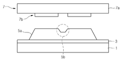
도 1a 내지 도 1c는 종래의 라인 패턴 불량을 설명하는 도면이다.1A to 1C are diagrams illustrating conventional line pattern defects.
도 1a에 도시한 바와 같이, 기판(1) 상에 라인 패턴을 형성하기 위한 박막(3)을 형성하고, 그 위에 감광막(5)을 형성한다.As shown in FIG. 1A, the
감광막(5) 상에 노광용 마스크(7)를 정렬한 후 노광용 마스크(7)에 광을 조사하는 노광 공정을 수행한다.After aligning the
노광용 마스크(7)는 쿼츠(quartz)를 포함하는 베이스 기판(7a) 상에 크롬으로 이루어진 마스크 패턴(7b)이 형성되어 있다. In the
라인 패턴을 좁히기 위해서는 노광용 마스크(7)의 마스크 패턴(7b) 사이 또한 좁도록 형성되어야 한다. In order to narrow the line pattern, it should also be formed so as to be narrow between the
노광 공정을 수행하는 경우, 도 1b에 도시한 바와 같이, 마스크 패턴(7b) 사이의 간격이 노광 분해 능력을 초과하였기 때문에 마스크 패턴(7b) 사이로 광이 제대로 투과되지 않게 되어 마스크 패턴(7b) 사이에 대응하는 감광막이 노광되지 않게 된다. 따라서, 현상 공정을 수행하는 경우, 마스크 패턴(7b) 사이에 대응하는 감광막이 제거되지 않게 되어, 감광막 패턴(5a) 사이가 서로 연결된 감광막 쇼트 영역(5b)이 형성되게 된다. In the case of performing the exposure process, as shown in FIG. 1B, since the interval between the
도 1c에 도시한 바와 같이, 상기 감광막 패턴(5a, 5b)을 마스크로 하여 식각 공정을 수행하는 경우, 상기 감광막 패턴(5a)에 대응하는 영역에는 라인 패턴(3a)이 형성되는데 반해 상기 감광막 패턴(5a) 사이에 대응하는 박막(3)은 제거되지 않아 패턴 쇼트 영역(3b)이 형성되므로, 라인 패턴(3a) 사이가 쇼트되는 불량이 발생하게 된다. As illustrated in FIG. 1C, when the etching process is performed using the
이와 같이, 라인 패턴(3a) 사이의 쇼트 불량으로 인해 패턴 사이의 거리를 좁히지 못함에 따라 개구율을 향상시킬 수 없는 문제가 있다.As described above, there is a problem in that the aperture ratio cannot be improved because the distance between the patterns is not narrowed due to the short defect between the line patterns 3a.
실시예는 노광 한계를 극복하여 패턴 간 거리를 최소하할 수 있는 패턴 형성 방법 및 박막 트랜지스터 어레이 기판의 제조 방법을 제공한다.The embodiment provides a pattern forming method and a method of manufacturing a thin film transistor array substrate capable of minimizing the distance between patterns by overcoming exposure limitations.
실시예는 패턴 간 쇼트 불량을 방지하는 패턴 형성 방법 및 박막 트랜지스터 어레이 기판의 제조 방법을 제공한다.The embodiment provides a method of forming a pattern and a method of manufacturing a thin film transistor array substrate that prevent short shorts between patterns.
실시예는 개구율을 향상시킬 수 있는 박막 트랜지스터 어레이 기판의 제조 방법을 제공한다.The embodiment provides a method of manufacturing a thin film transistor array substrate capable of improving the aperture ratio.
실시예에 따르면, 패턴 형성 방법은, 기판 상에 제1 및 제2 패턴을 형성하기 위한 박막을 형성하는 단계; 상기 박막 상에 감광막을 형성하는 단계; 상기 제1 및 제2 패턴 사이의 간격이 최소화되도록 상기 제1 및 제2 패턴 사이의 간격에 대응하는 반투과 영역을 포함하는 마스크를 정렬하는 단계; 상기 마스크에 광을 조사하여 상기 반투과 영역에 대응하는 상기 감광막의 상부 영역을 제거한 제1 감광 패턴을 형성하는 단계; 애싱 공정을 수행하여 상기 박막이 노출되도록 상기 반투과 영역에 대응하는 상기 제1 감광 패턴을 제거한 제2 감광 패턴을 형성하는 단계; 및 상기 제2 감광 패턴을 식각용 마스크로 하여 상기 박막을 패턴하여 상기 제1 및 제2 패턴을 형성하는 단계를 포함한다.According to an embodiment, a method of forming a pattern may include forming a thin film for forming first and second patterns on a substrate; Forming a photoresist film on the thin film; Arranging a mask including a semi-transmissive area corresponding to the gap between the first and second patterns such that the gap between the first and second patterns is minimized; Irradiating light onto the mask to form a first photosensitive pattern from which an upper region of the photosensitive film corresponding to the transflective region is removed; Performing an ashing process to form a second photosensitive pattern from which the first photosensitive pattern corresponding to the transflective region is removed to expose the thin film; And patterning the thin film using the second photosensitive pattern as an etching mask to form the first and second patterns.
실시예에 따르면, 박막 트랜지스터 어레이 기판의 제조 방법은, 기판 상에 게이트 라인 및 게이트 전극을 포함하는 게이트 패턴 그룹을 형성하는 단계; 상기 기판 상에 게이트 절연막을 형성하는 단계; 상기 게이트 절연막 상에 반도체층과 데이터 라인, 소스 전극 및 드레인 전극을 포함하는 데이터 패턴 그룹을 형성하는 단계; 상기 기판 상에 콘택홀을 포함하는 보호막을 형성하는 단계; 및 상기 보호막 상에 화소 전극을 형성하는 단계를 포함하고, 상기 게이트 라인 사이의 제1 간격, 상기 소스 전극과 드레인 전극 사이의 제2 간격 및 상기 화소 전극 사이의 제3 간격 중 적어도 하나 이상의 간격을 최소화하기 위해 상기 적어도 하나 이상의 간격에 대응하는 반투과 영역을 포함하는 마스크를 이용한다. According to an embodiment, a method of manufacturing a thin film transistor array substrate may include forming a gate pattern group including a gate line and a gate electrode on a substrate; Forming a gate insulating film on the substrate; Forming a data pattern group including a semiconductor layer, a data line, a source electrode, and a drain electrode on the gate insulating layer; Forming a protective layer including a contact hole on the substrate; And forming a pixel electrode on the passivation layer, and forming at least one of a first gap between the gate line, a second gap between the source electrode and a drain electrode, and a third gap between the pixel electrode. To minimize the use of a mask comprising a transflective area corresponding to the at least one gap.
실시예는 노광 한계를 극복하여 패턴 간 거리를 최소하할 수 있다.Embodiments can overcome exposure limitations to minimize the distance between patterns.
실시예는 패턴 간 쇼트 불량을 방지할 수 있다.Embodiments can prevent short defects between patterns.
실시예는 개구율을 향상시킬 수 있다.Embodiments can improve the aperture ratio.
도 1a 내지 도 1c는 종래의 라인 패턴 불량을 설명하는 도면이다.
도 2는 실시예에 따른 박막 트랜지스터 어레이 기판을 도시한 평면도이다.
도 3은 도 1의 박막 트랜지스터 어레이 기판을 도시한 단면도이다.
도 4a 내지 도 4d는 도 1의 박막 트랜지스터 어레이 기판의 제조 공정을 도시한 도면이다.
도 5a 내지 도 5d는 도 4a의 게이트 패턴 그룹의 제조 공정을 도시한 도면이다.
도 6a 내지 도 6e는 도 4b의 데이터 패턴 그룹의 제조 공정을 도시한 도면이다.
도 7a 내지 도 7d는 도 4d의 화소 전극의 제조 공정을 도시한 도면이다.
도 8a 내지 도 8c는 실시예에 적용되는 노광용 마스크를 도시한 도면이다.
도 9는 도 1의 박막 트랜지스터 어레이 기판에 의한 개구율 향상을 보여주는 도면이다.1A to 1C are diagrams illustrating conventional line pattern defects.
2 is a plan view illustrating a thin film transistor array substrate according to an embodiment.
3 is a cross-sectional view illustrating the thin film transistor array substrate of FIG. 1.
4A to 4D are diagrams illustrating a manufacturing process of the thin film transistor array substrate of FIG. 1.
5A through 5D are diagrams illustrating a manufacturing process of the gate pattern group of FIG. 4A.
6A through 6E are diagrams illustrating a manufacturing process of the data pattern group of FIG. 4B.
7A to 7D are diagrams illustrating a manufacturing process of the pixel electrode of FIG. 4D.
8A to 8C are diagrams showing an exposure mask applied to the embodiment.
9 is a view illustrating an improvement in aperture ratio by the thin film transistor array substrate of FIG. 1.
이하 첨부된 도면들을 참고하여 실시예를 상세히 설명한다.Hereinafter, exemplary embodiments will be described in detail with reference to the accompanying drawings.
도 2는 실시예에 따른 박막 트랜지스터 어레이 기판을 도시한 평면도이고, 도 3은 도 1의 박막 트랜지스터 어레이 기판을 도시한 단면도이다.2 is a plan view illustrating a thin film transistor array substrate according to an embodiment, and FIG. 3 is a cross-sectional view illustrating the thin film transistor array substrate of FIG. 1.
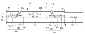
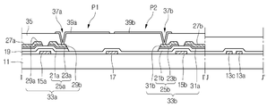
도 2를 참고하면, 실시예에 따른 박막 트랜지스터 어레이 기판(10)은 제1 게이트 라인(13a)과 제1 및 제2 데이터 라인(27a, 27b)에 의해 제1 및 제2 화소 영역(P1, P2)이 정의되고, 제2 게이트 라인(13b)과 제2 및 제3 데이터 라인(27b, 27c)에 의해 제3 및 제4 화소 영역(P3, P4)이 정의될 수 있다. Referring to FIG. 2, the thin film
상기 제1 데이터 라인(27a)은 상기 제1 화소 영역(P1)의 좌측 영역에 배치되고, 상기 제2 데이터 라인(27b)은 상기 제2 및 제3 화소 영역(P2, P3) 사이에 배치되며, 상기 제3 데이터 라인(27c)은 상기 제4 화소 영역(P4)의 우측 영역에 배치될 수 있다.The
상기 제1 게이트 라인(13a)과 상기 제1 데이터 라인(27a)에 제1 박막 트랜지스터(33a)가 전기적으로 연결되고, 상기 제1 게이트 라인(13a)과 상기 제2 데이터 라인(27b)에 제2 박막 트랜지스터(33b)가 전기적으로 연결될 수 있다. A first
상기 제2 게이트 라인(13b)과 상기 제2 데이터 라인(27b)에 제3 박막 트랜지스터(33c)가 전기적으로 연결되고, 상기 제2 게이트 라인(13b)과 상기 제3 데이터 라인(27c)에 제4 박막 트랜지스터(33d)가 전기적으로 연결될 수 있다. A third
상기 제1 화소 영역(P1)에는 상기 제1 박막 트랜지스터(33a)에 전기적으로 연결된 제1 화소 전극(39a)이 배치되고, 상기 제2 화소 영역(P2)에는 상기 제2 박막 트랜지스터(33b)에 전기적으로 연결된 제2 화소 전극(39b)이 배치될 수 있다.The
상기 제3 화소 영역(P3)에는 상기 제3 박막 트랜지스터(33c)에 전기적으로 연결된 제3 화소 전극(39c)이 배치되고, 제4 화소 영역(P4)에는 상기 제4 박막 트랜지스터(33d)에 전기적으로 연결된 제4 화소 전극(39d)이 배치될 수 있다. The
따라서, 제1 게이트 라인(13a)으로 인가된 게이트 신호에 응답하여 제1 및 제2 화소 영역(P1, P2)의 제1 및 제2 박막 트랜지스터(33a, 33b)가 턴온되고, 상기 제1 데이터 라인(27a)으로 공급된 제1 데이터 전압이 상기 제1 박막 트랜지스터(33a)를 경유하여 상기 제1 화소 전극(39a)으로 인가되고 상기 제2 데이터 라인(27b)으로 공급된 제2 데이터 전압이 상기 제2 박막 트랜지스터(33b)를 경유하여 상기 제2 화소 전극(39b)으로 인가될 수 있다. 상기 제1 화소 전극(39a)으로 인가된 제1 데이터 전압에 의해 상기 제1 화소 영역(P1)이 구동되고, 상기 제2 화소 전극(39b)으로 인가된 제2 데이터 전압에 의해 상기 제2 화소 영역(P2)이 구동될 수 있다. Accordingly, the first and second
상기 제2 게이트 라인(13b)으로 인가된 게이트 신호에 응답하여 상기 제3 및 제4 화소 영역(P3, P4)의 제3 및 제4 박막 트랜지스터(33c, 33d)가 턴온되고, 상기 제2 데이터 라인(27b)으로 인가된 제3 데이터 전압이 상기 제3 박막 트랜지스터(33c)를 경유하여 상기 제3 화소 전극(39c)으로 인가되고 상기 제3 데이터 라인(27c)으로 공급된 제4 데이터 전압이 상기 제4 박막 트랜지스터(33d)를 경유하여 상기 제4 화소 전극(39d)으로 인가될 수 있다. 상기 제3 화소 전극(39c)으로 인가된 제3 데이터 전압에 의해 상기 제3 화소 영역(P3)이 구동되며, 상기 제4 화소 전극(39d)으로 인가된 제4 데이터 전압에 의해 상기 제4 화소 영역(P4)이 구동될 수 있다. In response to the gate signal applied to the
각 화소 영역(P1 내지 P4)에는 화소 전극(39a 내지 39d)과의 오버랩에 의해 스토리지 캐패시터(Cst1, Cst2)를 형성하기 위한 공통 전극(17)이 배치될 수 있다. 상기 공통 전극(17)은 상기 각 화소 영역(P1 내지 P4)에서 상기 화소 전극(39a 내지 39d)의 에지 영역에 오버랩될 수 있다. In each pixel area P1 to P4, a
가로 방향(제1 방향)을 따라 각 화소 영역(P1 내지 P4)의 공통 전극(17)은 공통 연결 전극(17a)에 의해 전기적으로 연결될 수 있다. 상기 공통 연결 전극(17a)은 상기 공통 전극(17)과 일체로 형성될 수 있다. The
실시예는 제1 방향을 따라 한 쌍의 박막 트랜지스터(33a 및 33b, 33c 및 33d)가 제1 게이트 라인(13a)과 제2 게이트 라인(13b)에 교대로 연결되는 구조를 가질 수 있다. 예컨대 제1 및 제2 박막 트랜지스터(33a, 33b)는 제1 게이트 라인(13a)에 연결되고, 제3 및 제4 박막 트랜지스터(33c, 33d)는 제2 게이트 라인(13b)에 연결될 수 있다. The embodiment may have a structure in which a pair of
한편, 상기 제1 게이트 라인(13a)에 인접하여 상기 제1 게이트 라인(13a)과 평행하게 또 다른 게이트 라인(13c)이 배치될 수 있다. 따라서, 세로 방향(제2 방향)에서 화소 영역 사이에 서로 인접한 한 쌍의 게이트 라인들(13a, 13c)이 배치될 수 있다. Meanwhile, another
한 쌍의 게이트 라인(13a, 13c) 사이의 거리를 최소화할수록 화소 영역의 개구율은 향상될 수 있다. As the distance between the pair of
또한, 제1 및 제2 화소 전극(39a, 39b) 사이 그리고 제3 및 제4 화소 전극(39c, 39d) 사이의 거리를 최소화할수록 화소 영역의 개구율은 향상될 수 있다. In addition, as the distance between the first and
실시예는 게이트 라인(13a, 13c) 사이의 거리 및/또는 화소 전극(39a 및 39b, 39c 및 39d) 사이의 거리를 최소화하여 개구율을 향상시키기 위해 제안되었다. Embodiments have been proposed to improve the aperture ratio by minimizing the distance between the
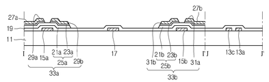
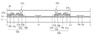
도 3에 도시한 바와 같이, 기판(11) 상에 제1 게이트 라인(미도시), 제1 및 제2 게이트 전극(15a, 15b) 및 공통 전극(17)이 형성되고, 상기 제1 및 제2 게이트 전극(15a, 15b) 상에 게이트 절연막(19)이 형성되고 그 위에 활성층(21a, 21b)과 오믹 콘택층(23a, 23b)을 포함하는 제1 및 제2 반도체층(25a, 25b)이 형성될 수 있다.As shown in FIG. 3, first gate lines (not shown), first and
상기 제1 반도체층(25a) 상에 제1 소스 전극(29a)과 제1 드레인 전극(29b)이 형성되고, 제2 반도체층(25b) 상에 제2 소스 전극(31a)과 제2 드레인 전극(32b)이 형성될 수 있다. 이와 함께 제1 데이터 라인(27a)과 제2 데이터 라인(27b)이 형성될 수 있다. The
상기 제1 게이트 전극(15a), 상기 제1 반도체층(25a), 상기 제1 소스 전극(29a) 및 상기 제1 드레인 전극(29b)에 의해 상기 제1 박막 트랜지스터(33a)가 형성되고, 상기 제2 게이트 전극(15b), 상기 제2 반도체층(25b), 상기 제2 소스 전극(31a) 및 상기 제2 드레인 전극(31b)에 의해 제2 박막 트랜지스터층(33b)이 형성될 수 있다.The first
상기 제1 및 제2 박막 트랜지스터(33a, 33b) 상에 보호막(35)이 형성되고, 상기 보호막(35)에 제1 콘택홀(37a)과 제2 콘택홀(37b)이 형성될 수 있다.A
상기 보호막(35) 상에 제1 콘택홀(37a)을 통해 상기 제1 드레인 전극(29b)에 전기적으로 연결된 제1 화소 전극(39a)과 제2 콘택홀(27b)을 통해 상기 제2 드레인 전극(31b)에 전기적으로 연결된 제2 화소 전극(39b)이 형성될 수 있다.The second drain electrode through the
따라서, 상기 제1 화소 영역(P1)에는 제1 게이트 라인(13a)과 제1 데이터 라인(27a)에 전기적으로 연결된 제1 박막 트랜지스터(33a)와 상기 제1 박막 트랜지스터(33a)에 전기적으로 연결된 제1 화소 전극(39a)이 형성되고, 상기 제2 화소 영역(P2)에는 제1 게이트 라인(13a)과 제2 데이터 라인(27b)에 전기적으로 연결된 제2 박막 트랜지스터(33b)와 상기 제2 박막 트랜지스터(33b)에 전기적으로 연결된 제2 화소 전극(39b)이 형성될 수 있다. Therefore, the first
이상과 같이 구성된 실시예에 따른 박막 트랜지스터 어레이 기판의 제조 공정을 도 4a 내지 도 4d를 참고하여 설명한다.The manufacturing process of the thin film transistor array substrate according to the embodiment configured as described above will be described with reference to FIGS. 4A to 4D.
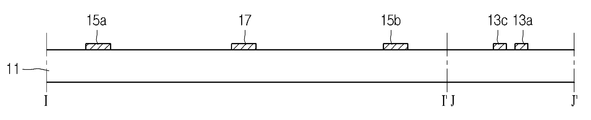
도 4a를 참고하면, 기판(11) 상에 제1 마스크 공정을 이용하여 게이트 라인(13a, 13c), 게이트 전극(15a, 15b) 및 공통 전극(17)을 포함하는 게이트 패턴그룹을 형성한다. Referring to FIG. 4A, a gate pattern group including the
제1 방향을 따라 배열된 화소 영역들(P1 내지 P4)이 가로 화소 영역들로 정의될 수 있다. 따라서, 다수의 가로 화소 영역들이 정의될 수 있다. Pixel areas P1 to P4 arranged along the first direction may be defined as horizontal pixel areas. Thus, a plurality of horizontal pixel regions can be defined.
다수의 게이트 라인들(13a 내지 13c)이 제1 방향을 따라 형성될 수 있다. A plurality of
이러한 경우, 제1 가로 화소 영역들의 상측과 하측에 제1 및 제2 게이트 라인들(13a, 13b)이 배치되고, 제2 가로 화소 영역들의 상측과 하측에 제3 게이트 라인(13c) 및 제4 게이트 라인이 배치될 수 수 있다. 상기 제1 및 상기 제3 게이트 라인들(13a, 13c)은 가능한 최대한 좁은 간격으로 이격되어 배치될 수 있다. 이와 같이 상기 제1 및 제3 게이트 라인들(13a,13c)의 간격을 최소화함으로써, 화소 영역의 개구율이 향상될 수 있다.In this case, the first and
게이트 패턴 그룹의 형성을 도 5a 내지 도 5를 참고하여 더욱 상세히 설명한다.Formation of the gate pattern group will be described in more detail with reference to FIGS. 5A to 5.
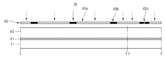
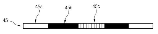
도 5a에 도시한 바와 같이, 기판(11) 상에 제1 금속막(41)과 제1 감광막(43)을 순차적으로 형성하고, 그 위에 제1 하프톤 마스크(halftone mask, HTM)(45)를 정렬한다.As shown in FIG. 5A, the
상기 제1 감광막(43)은 광에 의해 반응하여 제거되는 포지티브 감광막일 수 있다. 하지만, 실시예는 네거티브 감광막이 사용될 수도 있고, 이에 대해서는 한정하지 않는다.The
제1 하프톤 마스크(45)는 투과 영역(45a), 차단 영역(45b) 및 반투과 영역(45c)을 포함할 수 있다. 투과 영역(45a)은 광이 완전하게 투과되는 영역이고, 차단 영역(45b)은 광이 전혀 투과되지 않는 영역이며, 반투과 영역(45c)은 광이 회절되어 부분적으로 투과되는 영역일 수 있다. The
상기 반투과 영역(45c)은 다수의 미세한 슬릿(slit)을 포함하는 영역으로서, 매우 좁은 폭으로 설계될 수 있다. The
예컨대, 상기 반투과 영역(45c)은 6㎛이하의 폭으로 설계될 수 있다. For example, the
일반 마스크의 경우, 반투과 영역 대신에 투과 영역이 형성되는데, 이러한 투과 영역의 폭이 매우 좁은 경우 광이 조사되면 투과 영역에 대응하는 감광막이 노광의 분해 능력의 한계로 인해 투과 영역을 통해 감광막으로 조사되는 광량이 부족하여 감광막이 제거되지 않게 될 수 있다. 감광막이 제거되지 않게 되어 이후 식각 공정시 라인 쇼트 불량이 발생되는 문제가 있다. In the case of a general mask, a transmissive region is formed instead of a semi-transmissive region. When the width of the transmissive region is very narrow, when light is irradiated, a photosensitive film corresponding to the transmissive region passes through the transmissive region through the transmissive region due to the limitation of the resolution of exposure. The amount of light to be irradiated may be insufficient to prevent the photoresist from being removed. Since the photoresist is not removed, there is a problem that a line short defect occurs during the subsequent etching process.
매우 좁은 간격으로 감광막을 제거하는 경우, 일반 마스크의 투과 영역 대신에 하프톤 마스크(45)의 반투과 영역(45c)을 이용함으로써, 매우 좁은 간격의 감광막을 용이하게 제거할 수 있다.When the photosensitive film is removed at very narrow intervals, the
상기 제1 감광막(43)을 남기기 위한 영역에 대응하는 제1 하프톤 마스크(45)의 영역은 차단 영역(45b)이 위치되고, 상기 제1 감광막(43)을 제거하기 위한 영역에 대응하는 제1 하프톤 마스크(45)의 영역은 투과 영역(45a)이 위치되며, 게이트 라인 사이의 간격에 대응하는 제1 하프톤 마스크(45)의 영역은 반투과 영역(45c)이 위치될 수 있다. 상기 반투과 영역(45c)의 좌우측에는 인접하는 게이트 라인들에 대응하는 차단 영역들(45b)이 위치될 수 있다.In the region of the
상기 제1 하프톤 마스크(45)로 광을 조사하게 된다.Light is irradiated onto the
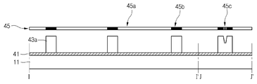
도 5b에 도시한 바와 같이, 상기 제1 하프톤 마스크(45)의 투과 영역(45a)을 통해 조사된 광에 의해 상기 투과 영역(45a)에 대응하는 제1 감광막(43)은 제거되고, 상기 제1 하프톤 마스크(45)의 차단 영역(45b)에 대응하는 제1 감광막(43)은 광이 조사되지 않기 때문에 제거되지 않게 된다. 또한 상기 제1 하프톤 마스크(45)의 반투과 영역(45c)에 대응하는 제1 감광막(43)은 투과 영역(45a)에 비해 투과되는 광량이 적기 때문에 제1 감광막(43)의 상부 영역이 국부적으로 제거될 수 있다. 따라서, 상기 제1 하프톤 마스크(45)가 차단 영역(45b)과 반투과 영역(45c)에 대응하는 제1 감광막(43)을 제외한 나머지 영역의 제1 감광막(43)이 제거된 제1 감광 패턴(43a)이 형성될 수 있다.As shown in FIG. 5B, the first
상기 제1 감광 패턴(43a)에서 상기 제1 하프톤 마스크(45)의 반투과 영역(45c)에 대응하는 제1 감광막(43)이 제거된 경우, 제거된 제1 감광막(43)의 폭은 상기 제1 하프톤 마스크(45)의 반투과 영역(45c)의 폭과 비슷한 6㎛이하가 될 수 있다.When the
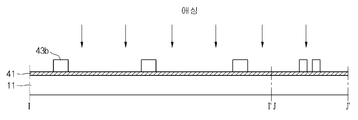
도 5c에 도시한 바와 같이, 상기 제1 하프톤 마스크(45)를 제거한 다음, 산소나 수소 플라즈마를 이용한 애싱 공정을 수행하여, 상기 제1 감광 패턴(43a)의 상부 영역을 제거하여 그 높이를 줄여준다. 상기 애싱 공정은 상기 제1 하프톤 마스크(45)의 반투과 영역(45c)에 대응하는 제1 감광 패턴(43a)의 영역이 완전히 제거되어 제1 금속막(41)이 노출될 때까지 수행될 수 있다. As shown in FIG. 5C, after removing the
상기 애싱 공정에 의해 게이트 라인, 게이트 전극 및 공통 전극을 형성하기 위한 영역에 대응하는 감광막만 남아 있는 제2 감광 패턴(43b)이 형성될 수 있다. By the ashing process, a second
특히 상기 제2 감광 패턴(43b)에서 인접하는 게이트 라인들에 대응하는 제1 감광 패턴(43a)은 높이는 줄어들었지만 완전히 제거되지 않고 감광 패턴으로 남아 있고, 게이트 라인들 사이의 간격에 대응하는 제1 감광 패턴(43a)은 완전히 제거될 수 있다. 따라서, 게이트 라인들에 대응하는 제1 감광 패턴(43a)만 남아 있고 상기 게이트 라인들 사이의 간격에 대응하는 제1 감광 패턴(43a)은 모두 제거되므로 감광 패턴의 쇼트가 발생되지 않게 된다. 또한, 제1 하프톤 마스크(45)에서 매우 좁은 간격(6㎛이하)으로 설계된 반투과 영역(45c)의 폭이 인접하는 게이트 라인들 사이의 간격에 대응하는 감광 패턴(43a) 사이의 폭으로 그대로 전사될 수 있다. In particular, the first
도 5d에 도시한 바와 같이, 제2 감광 패턴(43b)을 마스크로 하여 식각 공정을 수행하여 제1 금속막(41)을 부분적으로 제거한다. 이에 따라, 게이트 라인(13a, 13c), 게이트 전극(15a, 15b) 및 공통 전극(17)을 포함하는 게이트 패턴 그룹이 형성될 수 있다. 특히, 6㎛이하의 간격을 갖는 게이트 라인들(13a, 13c)을 형성할 수 있다. As shown in FIG. 5D, an etching process is performed using the second
따라서, 실시예는 제1 하프톤 마스크(45)를 이용하여 인접하는 게이트 라인들(13a, 13c) 사이의 간격을 최소화하여 화소 영역의 개구율을 극대화할 수 있다.Therefore, the exemplary embodiment may maximize the aperture ratio of the pixel area by minimizing the gap between the
도 4b를 참고하면, 게이트 패턴 그룹을 포함하는 기판(11) 상에 제2 마스크 공정을 이용하여 반도체층(25a, 25b)과 데이터 라인(27a, 27b), 소스 전극(29a, 31a) 및 드레인 전극(29b, 31b)을 포함하는 데이터 패턴 그룹을 형성한다. Referring to FIG. 4B, the semiconductor layers 25a and 25b, the
상기 기판(11) 상에 게이트 절연막(19)이 형성되고, 게이트 전극(15a, 15b)에 대응하는 게이트 절연막(19) 상에 반도체층(25a, 25b)이 형성되며, 상기 반도체층(25a,25b)을 포함하는 기판(11) 상에 데이터 라인(27a, 27b), 소스 전극(29a, 31a) 및 드레인 전극(29b, 31b)을 포함하는 데이터 패턴 그룹이 형성될 수 있다.A
상기 반도체층(25a, 25b)은 활성층(21a, 21b)과 오믹 콘택층(23a, 23b)을 포함할 수 있다. The semiconductor layers 25a and 25b may include
상기 데이터 라인(27a, 27b)은 상기 게이트 라인(13a, 13c)과 교차하여 화소 영역(P1 내지 P4)을 정의할 수 있다. The data lines 27a and 27b may cross the
예를 들어, 제1 게이트 라인(13a)과 제1 및 제2 데이터 라인(27a, 27b)에 의해 제1 및 제2 화소 영역들(P1, P2)이 정의될 수 있다. 제2 게이트 라인(13b)과 제2 및 제3 데이터 라인(27b, 27c)에 의해 제3 및 제4 화소 영역들(P3, P4)이 정의될 수 있다. For example, the first and second pixel regions P1 and P2 may be defined by the
상기 반도체층(25a, 25b)과 상기 데이터 패턴 그룹의 형성을 도 6a 내지 도 6e를 참고하여 더욱 상세히 설명한다.Formation of the semiconductor layers 25a and 25b and the data pattern group will be described in more detail with reference to FIGS. 6A to 6E.
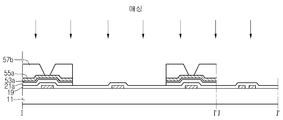
도 6a에 도시한 바와 같이, 게이트 라인(13a, 13c)을 포함하는 기판(11) 상에 게이트 절연막(19), 비정질막(51), 불순물을 포함하는 비정질막(53), 제2 금속막(55)과 제2 감광막(57)을 순차적으로 형성하고, 그 위에 제2 하프톤 마스크(59)를 정렬한다.As shown in FIG. 6A, the
상기 제2 감광막(57)은 광에 의해 반응하여 제거되는 포지티브 감광막일 수 있다. 하지만, 실시예는 네거티브 감광막이 사용될 수도 있고, 이에 대해서는 한정하지 않는다.The
제2 하프톤 마스크(59)는 투과 영역(59a), 차단 영역(59b) 및 반투과 영역(59c)을 포함할 수 있다. 투과 영역(59a)은 광이 완전하게 투과되는 영역이고, 차단 영역(59b)은 광이 전혀 투과되지 않는 영역이며, 반투과 영역(59c)은 광이 회절되어 부분적으로 투과되는 영역일 수 있다. The
상기 반투과 영역(59c)은 마수의 슬릿(slit)을 포함하는 영역으로서, 매우 좁은 폭으로 설계될 수 있다. The
예컨대, 상기 반투과 영역(59c)은 6㎛이하의 폭으로 설계될 수 있다. For example, the
상기 제2 감광막(57)을 남기기 위한 영역에 대응하는 제2 하프톤 마스크(59)의 영역은 차단 영역(59b)이 위치되고, 상기 제2 감광막(57)을 제거하기 위한 영역에 대응하는 제2 하프톤 마스크(59)의 영역은 투과 영역(59a)이 위치되며, 소스 전극과 드레인 전극 사이의 간격에 대응하는 제2 하프톤 마스크(59)의 영역은 반투과 영역(59c)이 위치될 수 있다. 상기 반투과 영역(59c)의 좌우측에는 인접하는 소스 전극과 드레인 전극에 대응하는 차단 영역들(59b)이 위치될 수 있다.In the region of the
상기 제2 하프톤 마스크(59)로 광을 조사하게 된다.Light is irradiated onto the
도 6b에 도시한 바와 같이, 상기 제2 하프톤 마스크(59)의 투과 영역(59a)을 통해 조사된 광에 의해 상기 투과 영역(59a)에 대응하는 제2 감광막(57)은 제거되고, 상기 제2 하프톤 마스크(59)의 차단 영역(59b)에 대응하는 제2 감광막(57)은 광이 조사되지 않기 때문에 제거되지 않게 된다. 또한 상기 제2 하프톤 마스크(59)의 반투과 영역(59c)에 대응하는 제2 감광막(57)은 투과 영역(59a)에 비해 투과되는 광량이 적기 때문에 제2 감광막(57)의 상부 영역이 국부적으로 제거될 수 있다. 따라서, 상기 제2 하프톤 마스크(59)이 차단 영역(59b)과 반투과 영역(59c)에 대응하는 제2 감광막(57)을 제외한 나머지 영역의 제2 감광막(57)이 제거된 제1 감광 패턴(57a)이 형성될 수 있다.As shown in FIG. 6B, the second
상기 제1 감광 패턴(57a)에서 상기 제2 하프톤 마스크(59)의 반투과 영역(59c)에 대응하는 제2 감광막(57)이 제거된 경우, 제거된 제2 감광막(57)의 폭은 상기 제2 하프톤 마스크(59)의 반투과 영역(59c)의 폭과 비슷한 6㎛이하가 될 수 있다.When the second
도 6c에 도시한 바와 같이, 상기 제2 하프톤 마스크(59)를 제거한 다음, 제1 감광 패턴(57a)을 마스크로 하여 1차 식각 공정을 수행하여, 상기 제2 하프톤 마스크(59)의 투과 영역(59a)에 대응하는 제2 금속막(55), 불순물을 포함하는 비정질막(53) 및 비정질막(51)을 제거하여 제2 금속 패턴(55a)과 비정질 패턴(53a)이 형성된다. 상기 제2 금속막(55)의 제거에 의해 데이터 라인(27a, 27b)이 형성되고, 비정질막(51)의 제거에 의해 활성층(21a, 21b)이 형성될 수 있다. As shown in FIG. 6C, the
도 6d에 도시한 바와 같이, 산소나 수소 플라즈마를 이용한 애싱 공정을 수행하여, 상기 제1 감광 패턴(57a)의 상부 영역을 제거하여 그 높이를 줄여준다. 상기 애싱 공정은 상기 제2 하프톤 마스크(59)의 반투과 영역(59c)에 대응하는 제1 감광 패턴(57a)의 영역이 완전히 제거되어 제2 금속 패턴(55a)이 노출될 때까지 수행될 수 있다. As shown in FIG. 6D, an ashing process using oxygen or hydrogen plasma is performed to remove the upper region of the first
상기 애싱 공정에 의해 오믹 콘택층, 소스 전극 및 드레인 전극을 형성하기 위한 영역에 대응하는 감광막만 남아 있는 제2 감광 패턴(57b)이 형성될 수 있다. By the ashing process, a second
특히 상기 제2 감광 패턴(57b)에서 인접하는 소스 전극과 드레인 전극에 대응하는 제1 감광 패턴(57a)은 높이는 줄어들었지만 완전히 제거되지 않고 감광 패턴으로 남아 있고, 소스 전극과 드레인 전극 사이의 간격에 대응하는 제1 감광 패턴(57a)은 완전히 제거될 수 있다. 따라서, 소스 전극과 드레인 전극에 대응하는 제1 감광 패턴(57a)만 남아 있고 소스 전극과 드레인 전극 사이의 간격에 대응하는 제1 감광 패턴(57a)은 모두 제거되므로 감광 패턴의 쇼트가 발생되지 않게 된다. 또한, 제2 하프톤 마스크(59)에서 매우 좁은 간격(6㎛이하)으로 설계된 반투과 영역(59c)의 폭이 인접하는 소스 전극과 드레인 전극 사이의 간격에 대응하는 감광 패턴(57a) 사이의 폭으로 그대로 전사될 수 있다. In particular, the first
도 6e에 도시한 바와 같이, 제2 감광 패턴(57b)을 마스크로 하여 식각 공정을 수행하여 제2 하프톤 마스트(59)의 반투과 영역(59c)에 대응하는 제2 금속 패턴(55a)과 불순물을 포함하는 비정질 패턴(53a)을 제거한다. 이에 따라, 소스 전극(29a, 31a)과 드레인 전극(29b, 31b) 그리고 오믹 콘택층(23a, 23b)이 형성될 수 있다. As shown in FIG. 6E, an etching process is performed using the second
제2 마스크 공정을 이용하여 반도체층(25a, 25b)과 더불어 데이터 라인(27a, 27b), 소스 전극(29a, 31a) 및 드레인 전극(29b, 31b)을 포함하는 데이터 패턴 그룹을 형성할 수 있다. 특히, 6㎛이하의 간격을 갖는 소스 전극(29a, 31a)과 드레인 전극(29b, 31b)을 형성할 수 있다. A data pattern group including the
따라서, 실시예는 제2 하프톤 마스크(59)를 이용하여 인접하는 소스 전극(29a, 31a)과 드레인 전극(29b, 31b) 사이의 간격을 최소화하여 화소 영역의 개구율을 극대화할 수 있다.Therefore, the embodiment can maximize the aperture ratio of the pixel region by minimizing the distance between the
도 4c를 참고하면, 데이터 패턴 그룹을 포함하는 기판(11) 상에 제3 마스크 공정을 이용하여 보호막(35)에 콘택홀(37a, 37b)을 형성한다. Referring to FIG. 4C,
기판(11) 상에 유기 물질이나 금속 물질로 이루어지는 보호막(35)을 형성하고, 그 위에 노멀 마스크를 정렬한 다음, 노광 공정을 수행하여 콘택홀(37a, 37b)을 형성할 수 있다.The
상기 콘택홀(37a, 37b)은 상기 드레인 전극(29b, 31b)이 노출되도록 형성될 수 있다. The contact holes 37a and 37b may be formed to expose the
노멀 마스크는 반투과 영역은 존재하지 않고 투과 영역과 차단 영역만 존재하는 마스크를 의미할 수 있다.The normal mask may refer to a mask in which only a transmissive region and a blocking region exist without a transflective region.
도 4d를 참고하면, 보호막(35) 상에 제4 마스크 공정을 이용하여 화소 전극(39a, 39b)을 형성한다.Referring to FIG. 4D,
상기 화소 전극(39a, 39b)의 형성을 도 도 7a 내지 도 7d를 참고하여 더욱 상세히 설명한다.Formation of the
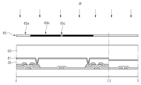
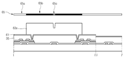
도 7a에 도시한 바와 같이, 상기 보호막(35) 상에 투명한 도전막(61)과 제3 감광막(63)을 순차적으로 형성한 후, 그 위에 제3 하프톤 마스크(65)를 정렬한다.As shown in FIG. 7A, the transparent
상기 제3 감광막(63)은 광에 의해 반응하여 제거되는 포지티브 감광막일 수 있다. 하지만, 실시예는 네거티브 감광막이 사용될 수도 있고, 이에 대해서는 한정하지 않는다.The
제3 하프톤 마스크(65)는 투과 영역(65a), 차단 영역(65b) 및 반투과 영역(65c)을 포함할 수 있다. 투과 영역(65a)은 광이 완전하게 투과되는 영역이고, 차단 영역(65b)은 광이 전혀 투과되지 않는 영역이며, 반투과 영역(65c)은 광이 회절되어 부분적으로 투과되는 영역일 수 있다. The
상기 반투과 영역(65c)은 다수의 슬릿(slit)을 포함하는 영역으로서, 매우 좁은 폭으로 설계될 수 있다. The
예컨대, 상기 반투과 영역(65c)은 6㎛이하의 폭으로 설계될 수 있다. For example, the
상기 제3 감광막(63)을 남기기 위한 영역에 대응하는 제3 하프톤 마스크(65)의 영역은 차단 영역(65b)이 위치되고, 상기 제3 감광막(63)을 제거하기 위한 영역에 대응하는 제3 하프톤 마스크(65)의 영역은 투과 영역(65a)이 위치되며, 화소 전극 사이의 간격에 대응하는 제3 하프톤 마스크(65)의 영역은 반투과 영역(65c)이 위치될 수 있다. 상기 반투과 영역(65c)의 좌우측에는 인접하는 화소 전극들에 대응하는 차단 영역들(65b)이 위치될 수 있다.In the region of the
상기 제3 하프톤 마스크(65)로 광을 조사하게 된다.Light is irradiated onto the
도 7b에 도시한 바와 같이, 상기 제3 하프톤 마스크(65)의 투과 영역(65a)을 통해 조사된 광에 의해 상기 투과 영역(65a)에 대응하는 제3 감광막(63)은 제거되고, 상기 제3 하프톤 마스크(65)의 차단 영역(65b)에 대응하는 제3 감광막(63)은 광이 조사되지 않기 때문에 제거되지 않게 된다. 또한 상기 제3 하프톤 마스크(65)의 반투과 영역(65c)에 대응하는 제3 감광막(63)은 투과 영역에 비해 투과되는 광량이 적기 때문에 제3 감광막(63)의 상부 영역이 국부적으로 제거될 수 있다. 따라서, 상기 제3 하프톤 마스크(65)이 차단 영역(65b)과 반투과 영역(65c)에 대응하는 제3 감광막(63)을 제외한 나머지 영역의 제3 감광막(63)이 제거된 제1 감광 패턴(63a)이 형성될 수 있다.As shown in FIG. 7B, the third
상기 제1 감광 패턴(63a)에서 상기 제3 하프톤 마스크(65)의 반투과 영역(65c)에 대응하는 제3 감광막(63)이 제거된 경우, 제거된 제3 감광막(63)의 폭은 상기 제3 하프톤 마스크(65)의 반투과 영역(65c)의 폭과 비슷한 6㎛이하가 될 수 있다.When the
도 7c에 도시한 바와 같이, 상기 제3 하프톤 마스크(65)를 제거한 다음, 산소나 수소 플라즈마를 이용한 애싱 공정을 수행하여, 상기 제1 감광 패턴(63a)의 상부 영역을 제거하여 그 높이를 줄여준다. 상기 애싱 공정은 상기 제3 하프톤 마스크(65)의 반투과 영역(65c)에 대응하는 제1 감광 패턴(63a)의 영역이 완전히 제거되어 투명한 도전막(61)이 노출될 때까지 수행될 수 있다. As shown in FIG. 7C, after removing the
상기 애싱 공정에 의해 화소 전극을 형성하기 위한 영역에 대응하는 제1 감광 패턴(63a)만 남아 있는 제2 감광 패턴(63b)이 형성될 수 있다. The second
특히 상기 제2 감광 패턴(63b)에서 인접하는 화소 전극들에 대응하는 제1 감광 패턴(63a)은 높이는 줄어들었지만 완전히 제거되지 않고 감광 패턴으로 남아 있고, 화소 전극들 사이의 간격에 대응하는 제1 감광 패턴(63a)은 완전히 제거될 수 있다. 따라서, 화소 전극들에 대응하는 제1 감광 패턴(63a)만 남아 있고 상기 화소 전극들 사이의 간격에 대응하는 제1 감광 패턴(63a)은 모두 제거되므로 감광 패턴의 쇼트가 발생되지 않게 된다. 또한, 제3 하프톤 마스크(65)에서 매우 좁은 간격(6㎛이하)으로 설계된 반투과 영역(65c)의 폭이 인접하는 화소 전극 사이의 간격에 대응하는 감광 패턴(63a) 사이의 폭으로 그대로 전사될 수 있다. In particular, the first
도 7d에 도시한 바와 같이, 제2 감광 패턴(63b)을 마스크로 하여 식각 공정을 수행하여 투명한 도전막(61)을 부분적으로 제거한다. 이에 따라, 6㎛ 이하의 간격을 갖는 화소 전극들(39a, 39b)이 형성될 수 있다. As shown in FIG. 7D, an etching process is performed using the second
따라서, 실시예는 제3 하프톤 마스크(65)를 이용하여 인접하는 화소 전극들(39a, 39b) 사이의 간격을 최소화하여 화소 영역의 개구율을 극대화할 수 있다.Therefore, the embodiment can maximize the aperture ratio of the pixel region by minimizing the gap between the
이상의 실시예는 라인 패턴 사이의 간격을 최소화하기 위해 하프톤 마스크가 사용되었다.In the above embodiment, a halftone mask is used to minimize the spacing between the line patterns.
하지만, 실시예는 하프톤 이외의 다른 마스크들이 추가적으로 사용될 수 있다.However, the embodiment may additionally use masks other than halftones.
도 8a는 이미 설명한 하프톤 마스크(45)이다. 하프톤 마스크(45)는 광이 완전히 투과되는 투과 영역(45a), 광이 완전히 차단되는 차단 영역(45b) 그리고 광이 회절되어 부분적으로 투과되는 반투과 영역(45c)을 포함할 수 있다. 상기 반투과 영역(45c)은 다수의 슬릿을 포함할 수 있다. 이에 따라, 광이 다수의 슬릿을 통해 회절되면서 광량이 줄어들게 된다.8A shows the
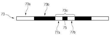
도 8b는 그레이 톤 마스크(73)이다. 그레이 톤 마스크(gray tone mask, GTM)(73)은 싱글 슬릿 마스크(single slit mask, SSM)과 유사하거나 동일할 수 있다.8B is a
그레이 톤 마스크(73)는 투과 영역(73a), 차단 영역(73b) 및 반투과 영역(73c)을 포함할 수 있다. The
상기 반투과 영역(73c)은 하나의 슬릿(75)과 슬릿(75)의 양측의 제1 및 제2 투과홀(77a, 77b)을 포함할 수 있다. 이에 따라, 광이 제1 및 제2 투과홀(77a, 77b)을 통해 회절되면서 광량이 줄어들게 된다.The
슬릿(75)의 폭과 제1 및 제2 투과홀(77a, 77b)의 폭을 조절하여 원하는 광량을 얻을 수 있다. A desired amount of light can be obtained by adjusting the width of the
도 8c는 비대칭 하프톤 마스크(asymmetric halftone mask, ASHM)(83)이다. 비대칭 하프톤 마스크(83)는 투과 영역(83a), 차단 영역(83b) 및 반투과 영역(83c)을 포함할 수 있다. 8C is an asymmetric halftone mask (ASHM) 83. The
상기 반투과 영역(83c)은 다수의 슬릿을 포함하는 제1 슬릿군(slit group)(85), 다수의 슬릿을 포함하고 상기 제1 슬릿군(85)의 폭보다 적어도 작은 제2 슬릿군(87) 및 상기 제1 및 제2 슬릿군(85, 87) 사이의 투과홀(89)을 포함할 수 있다. 상기 투과홀(89) 대신에 제1 및 제2 슬릿군(85, 87)에 포함된 슬릿에 비해 상대적으로 큰 폭을 갖는 하나의 슬릿이 사용될 수도 있다. The
상기 제1 및 제2 슬릿군(85, 87)은 서로 상이한 폭을 가지므로, 상기 제1 슬릿군(85)에서 회절되는 광과 상기 제2 슬릿군(87)에서 회절되는 광 사이의 회절량이 상이할 수 있다. Since the first and
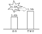
도 9에 도시한 바와 같이, 이상의 실시예에 의한 박막 트랜지스터 어레이 기판은 종래에 비해 대략 5.32% 정도 향상됨을 확인하였다. As shown in FIG. 9, the thin film transistor array substrate according to the above embodiment was confirmed to be improved by about 5.32% compared with the related art.
실시예의 박막 트랜지스터 어레이 기판에서 게이트 라인 사이의 간격 또는 화소 전극 사이의 간격은 종래에 비해 적어도 2㎛이하로 줄일 수 있고, 이와 같이 게이트 라인 사이의 간격 또는 화소 전극 사이의 간격이 종래에 비해 줄어들기 때문에 개구율이 향상될 수 있다. In the thin film transistor array substrate of the embodiment, the spacing between the gate lines or the spacing between the pixel electrodes can be reduced to at least 2 μm or less, and thus, the spacing between the gate lines or the spacing between the pixel electrodes can be reduced. Therefore, the aperture ratio can be improved.
실시예는 게이트 라인 사이의 간격을 줄이거나 화소 전극 사이의 간격을 줄이는 것에 한정하여 설명하고 있지만, 실시예는 이에 한정하지 않는다. 즉, 실시예는 공통 전극 또는 공통 라인 사이의 간격을 줄이는 데에도 적용될 수 있다. Embodiments have been described as being limited to reducing the gap between the gate lines or the gap between the pixel electrodes, but the embodiment is not limited thereto. That is, the embodiment can also be applied to reducing the spacing between common electrodes or common lines.
실시예는 도 1에서 도시된 박막 트랜지스터 어레이 기판의 구조 이외에 게이트 라인 사이의 간격, 공통 라인 사이의 간격, 화소 전극 사이의 간격 등과 같이 라인 패턴 사이의 간격을 줄여 개구율을 향상시키기 위한 어떠한 박막 트랜지스터 어레이 기판의 구조에도 동일하게 적용될 수 있다. The embodiment is any thin film transistor array for improving the aperture ratio by reducing the gap between the line patterns, such as the gap between the gate lines, the gap between the common lines, the gap between the pixel electrodes, etc., in addition to the structure of the thin film transistor array substrate shown in FIG. The same can be applied to the structure of the substrate.
10: 박막 트랜지스터 어레이 기판 11: 기판
13a, 13b, 13c: 게이트 라인 15a, 15b: 게이트 전극
17: 공통 전극 17a: 연결 전극
19: 게이트 절연막 21a, 21b: 활성층
23a, 23b: 오믹 콘택층 25a, 25b: 반도체층
27a, 27b, 27c: 데이터 라인 29a, 31a: 소스 전극
29b, 31b: 드레인 전극 35: 보호막
37a, 37b: 콘택홀 39a, 39b; 화소 전극10: thin film transistor array substrate 11: substrate
13a, 13b, 13c:
17: common electrode 17a: connection electrode
19:
23a, 23b:
27a, 27b, 27c:
29b, 31b: drain electrode 35: protective film
37a, 37b:
Claims (11)
상기 박막 상에 감광막을 형성하는 단계;
상기 제1 및 제2 패턴 사이의 간격이 최소화되도록 상기 제1 및 제2 패턴 사이의 간격에 대응하는 반투과 영역을 포함하는 마스크를 정렬하는 단계;
상기 마스크에 광을 조사하여 상기 반투과 영역에 대응하는 상기 감광막의 상부 영역을 제거한 제1 감광 패턴을 형성하는 단계;
애싱 공정을 수행하여 상기 박막이 노출되도록 상기 반투과 영역에 대응하는 상기 제1 감광 패턴을 제거한 제2 감광 패턴을 형성하는 단계; 및
상기 제2 감광 패턴을 식각용 마스크로 하여 상기 박막을 패턴하여 상기 제1 및 제2 패턴을 형성하는 단계
를 포함하는 패턴 형성 방법.Forming a thin film for forming first and second patterns on the substrate;
Forming a photoresist film on the thin film;
Arranging a mask including a semi-transmissive area corresponding to the gap between the first and second patterns such that the gap between the first and second patterns is minimized;
Irradiating light onto the mask to form a first photosensitive pattern from which an upper region of the photosensitive film corresponding to the transflective region is removed;
Performing an ashing process to form a second photosensitive pattern from which the first photosensitive pattern corresponding to the transflective region is removed to expose the thin film; And
Patterning the thin film using the second photosensitive pattern as an etching mask to form the first and second patterns
Pattern forming method comprising a.
상기 마스크는 하프톤 마스크, 그레이 톤 마스크 및 비대칭 하프톤 마스크 중 하나인 패턴 형성 방법.The method of claim 1,
And the mask is one of a halftone mask, a graytone mask, and an asymmetric halftone mask.
상기 기판 상에 게이트 절연막을 형성하는 단계;
상기 게이트 절연막 상에 반도체층과 데이터 라인, 소스 전극 및 드레인 전극을 포함하는 데이터 패턴 그룹을 형성하는 단계;
상기 기판 상에 콘택홀을 포함하는 보호막을 형성하는 단계; 및
상기 보호막 상에 화소 전극을 형성하는 단계를 포함하고,
상기 게이트 라인 사이의 제1 간격, 상기 소스 전극과 드레인 전극 사이의 제2 간격 및 상기 화소 전극 사이의 제3 간격 중 적어도 하나 이상의 간격을 최소화하기 위해 상기 적어도 하나 이상의 간격에 대응하는 반투과 영역을 포함하는 마스크를 이용하는 박막 트랜지스터 어레이 기판의 제조 방법.Forming a gate pattern group including a gate line and a gate electrode on the substrate;
Forming a gate insulating film on the substrate;
Forming a data pattern group including a semiconductor layer, a data line, a source electrode, and a drain electrode on the gate insulating layer;
Forming a protective layer including a contact hole on the substrate; And
Forming a pixel electrode on the passivation layer,
A semi-transmissive region corresponding to the at least one gap is minimized to minimize at least one of the first gap between the gate line, the second gap between the source electrode and the drain electrode, and the third gap between the pixel electrode. A method of manufacturing a thin film transistor array substrate using a mask comprising.
상기 마스크는 하프톤 마스크, 그레이 톤 마스크 및 비대칭 하프톤 마스크 중 하나인 박막 트랜지스터 어레이 기판의 제조 방법.The method of claim 3,
And the mask is one of a halftone mask, a graytone mask, and an asymmetric halftone mask.
상기 반투과 영역은 다수의 슬릿을 포함하는 박막 트랜지스터 어레이 기판의 제조 방법.The method of claim 3,
The transflective region includes a plurality of slits.
상기 반투과 영역은 슬릿과 상기 슬릿의 양측에 제1 및 제2 투과홀을 포함하는 박막 트랜지스터 어레이 기판의 제조 방법.The method of claim 3,
The transflective region includes a slit and first and second transmission holes on both sides of the slit.
상기 반투과 영역은 다수의 슬릿을 포함하는 제1 슬릿군, 다수의 슬릿을 포함하고 상기 제1 슬릿군과 상이한 폭을 갖는 제2 슬릿군 및 상기 제1 및 제2 슬릿군 사이의 투과홀을 포함하는 박막 트랜지스터 어레이 기판의 제조 방법.The method of claim 3,
The transflective area may include a first slit group including a plurality of slits, a second slit group including a plurality of slits and having a width different from that of the first slit group, and a transmission hole between the first and second slit groups. Method of manufacturing a thin film transistor array substrate comprising.
상기 반투과 영역은 다수의 슬릿을 포함하는 제1 슬릿군, 다수의 슬릿을 포함하고 상기 제1 슬릿군과 상이한 폭을 갖는 제2 슬릿군 및 상기 제1 및 제2 슬릿군에 포함된 슬릿보다 큰 폭을 갖고 상기 제1 및 제2 슬릿군 사이에 배치된 하나의 슬릿을 포함하는 박막 트랜지스터 어레이 기판의 제조 방법.The method of claim 3,
The semi-transmissive region may include a first slit group including a plurality of slits, a second slit group including a plurality of slits and having a different width than the first slit group, and a slit included in the first and second slit groups. A method of manufacturing a thin film transistor array substrate having a large width and including one slit disposed between the first and second slit groups.
상기 게이트 패턴 그룹을 형성하는 단계는,
상기 기판 상에 상기 게이트 라인 및 상기 게이트 전극을 형성하기 위한 제1 금속막과 제1 감광막을 형성하는 단계;
상기 제1 감광막 상에 상기 게이트 라인 사이의 간격에 대응하는 반투과 영역을 포함하는 제1 마스크를 정렬하는 단계;
상기 제1 마스크에 광을 조사하여 상기 반투과 영역에 대응하는 상기 제1 감광막의 상부 영역을 제거한 제1 감광 패턴을 형성하는 단계;
애싱 공정을 수행하여 상기 제1 금속막이 노출되도록 상기 반투과 영역에 대응하는 상기 제1 감광 패턴을 제거한 제2 감광 패턴을 형성하는 단계; 및
상기 제2 감광 패턴을 식각용 마스크로 하여 상기 제1 금속막을 패턴하여 상기 게이트 라인 및 상기 게이트 전극을 형성하는 단계
를 포함하는 박막 트랜지스터 어레이 기판의 제조 방법.The method of claim 3,
Forming the gate pattern group,
Forming a first metal film and a first photosensitive film on the substrate to form the gate line and the gate electrode;
Aligning a first mask including a transflective region corresponding to a gap between the gate lines on the first photoresist;
Irradiating light to the first mask to form a first photosensitive pattern from which an upper region of the first photosensitive film corresponding to the transflective region is removed;
Performing a ashing process to form a second photosensitive pattern from which the first photosensitive pattern corresponding to the transflective region is removed to expose the first metal film; And
Patterning the first metal layer using the second photosensitive pattern as an etching mask to form the gate line and the gate electrode
Method of manufacturing a thin film transistor array substrate comprising a.
상기 반도체층과 상기 데이터 패턴 그룹을 형성하는 단계는,
상기 게이트 절연막 상에 비정질막, 불순물을 포함하는 비정질막, 상기 데이터 라인, 상기 소스 전극 및 상기 드레인 전극을 형성하기 위한 제2 금속막 및 제2 감광막을 형성하는 단계;
상기 제2 감광막 상에 상기 소스 전극과 상기 드레인 전극 사이의 간격에 대응하는 반투과 영역을 포함하는 제2 마스크를 정렬하는 단계;
상기 제2 마스크에 광을 조사하여 상기 반투과 영역에 대응하는 상기 제2 감광막의 상부 영역을 제거한 제1 감광 패턴을 형성하는 단계;
상기 제1 감광 패턴을 제1 식각용 마스크로 하여 상기 제2 금속막, 상기 불순물을 포함하는 비정질막 및 상기 비정질막을 패턴하여 상기 데이터 라인과 상기 반도체층의 활성층을 형성하는 단계;
애싱 공정을 수행하여 상기 제1 금속막이 노출되도록 상기 반투과 영역에 대응하는 상기 제1 감광 패턴을 제거한 제2 감광 패턴을 형성하는 단계; 및
상기 제2 감광 패턴을 제2 식각용 마스크로 하여 상기 제1 금속막과 상기 불순물을 포함하는 비정질막을 패턴하여 상기 반도체층의 오믹 콘택층, 상기 소스 전극 및 상기 드레인 전극을 형성하는 단계
를 포함하는 박막 트랜지스터 어레이 기판의 제조 방법.The method of claim 3,
Forming the semiconductor layer and the data pattern group,
Forming an amorphous film, an amorphous film including impurities, a second metal film and a second photosensitive film for forming the data line, the source electrode and the drain electrode on the gate insulating film;
Arranging a second mask including a transflective region corresponding to a gap between the source electrode and the drain electrode on the second photosensitive film;
Irradiating light onto the second mask to form a first photosensitive pattern from which an upper region of the second photosensitive film corresponding to the transflective region is removed;
Forming an active layer of the data line and the semiconductor layer by patterning the second metal layer, the amorphous layer including the impurity, and the amorphous layer using the first photosensitive pattern as a first etching mask;
Performing a ashing process to form a second photosensitive pattern from which the first photosensitive pattern corresponding to the transflective region is removed to expose the first metal film; And
Forming an ohmic contact layer, the source electrode, and the drain electrode of the semiconductor layer by patterning an amorphous layer including the first metal layer and the impurities using the second photosensitive pattern as a second etching mask.
Method of manufacturing a thin film transistor array substrate comprising a.
상기 화소 전극을 형성하는 단계는,
상기 보호막 상에 상기 화소 전극을 형성하기 위한 도전막과 제3 감광막을 형성하는 단계;
상기 제3 감광막 상에 상기 화소 전극 사이의 간격에 대응하는 반투과 영역을 포함하는 제3 마스크를 정렬하는 단계;
상기 제3 마스크에 광을 조사하여 상기 반투과 영역에 대응하는 상기 제3 감광막의 상부 영역을 제거한 제1 감광 패턴을 형성하는 단계;
애싱 공정을 수행하여 상기 제3 금속막이 노출되도록 상기 반투과 영역에 대응하는 상기 제1 감광 패턴을 제거한 제2 감광 패턴을 형성하는 단계; 및
상기 제2 감광 패턴을 식각용 마스크로 하여 상기 도전막을 패턴하여 상기 화소 전극을 형성하는 단계
를 포함하는 박막 트랜지스터 어레이 기판의 제조 방법.The method of claim 3,
Forming the pixel electrode,
Forming a conductive film and a third photosensitive film for forming the pixel electrode on the passivation film;
Arranging a third mask including a transflective region corresponding to a gap between the pixel electrodes on the third photoresist;
Irradiating light onto the third mask to form a first photosensitive pattern from which an upper region of the third photosensitive film corresponding to the transflective region is removed;
Performing a ashing process to form a second photosensitive pattern from which the first photosensitive pattern corresponding to the transflective region is removed to expose the third metal film; And
Patterning the conductive layer using the second photosensitive pattern as an etching mask to form the pixel electrode
Method of manufacturing a thin film transistor array substrate comprising a.
Priority Applications (1)
| Application Number | Priority Date | Filing Date | Title |
|---|---|---|---|
| KR1020100137131A KR20120081663A (en) | 2010-12-28 | 2010-12-28 | Method of forming patterns and method of fabricating a thin film transistor array substrate |
Applications Claiming Priority (1)
| Application Number | Priority Date | Filing Date | Title |
|---|---|---|---|
| KR1020100137131A KR20120081663A (en) | 2010-12-28 | 2010-12-28 | Method of forming patterns and method of fabricating a thin film transistor array substrate |
Publications (1)
| Publication Number | Publication Date |
|---|---|
| KR20120081663A true KR20120081663A (en) | 2012-07-20 |
Family
ID=46713702
Family Applications (1)
| Application Number | Title | Priority Date | Filing Date |
|---|---|---|---|
| KR1020100137131A Ceased KR20120081663A (en) | 2010-12-28 | 2010-12-28 | Method of forming patterns and method of fabricating a thin film transistor array substrate |
Country Status (1)
| Country | Link |
|---|---|
| KR (1) | KR20120081663A (en) |
-
2010
- 2010-12-28 KR KR1020100137131A patent/KR20120081663A/en not_active Ceased
Similar Documents
| Publication | Publication Date | Title |
|---|---|---|
| JP4607418B2 (en) | Array substrate for liquid crystal display device and manufacturing method thereof | |
| JP4343510B2 (en) | Liquid crystal display device, thin film transistor substrate for liquid crystal display device and manufacturing method thereof | |
| KR100816333B1 (en) | Color filter substrates and thin film transistor substrates for liquid crystal display devices and methods of manufacturing the same | |
| KR101264722B1 (en) | Method for manufacturing Liquid Crystal Display Device | |
| TWI494677B (en) | Array substrate of liquid crystal display and manufacturing method thereof | |
| CN101369588B (en) | Thin film transistor array panel and manufacturing method thereof | |
| EP3187929A1 (en) | Array substrate and manufacturing method therefor, and display apparatus | |
| WO2017133097A1 (en) | Array substrate, preparation method therefor, and display panel | |
| US8203674B2 (en) | Manufacturing thin film transistor array panels for flat panel displays | |
| KR101450803B1 (en) | Array substrate and method for manufacturing the array substrate | |
| KR100978260B1 (en) | LCD and its manufacturing method | |
| US7855033B2 (en) | Photo mask and method of fabricating array substrate for liquid crystal display device using the same | |
| KR101682432B1 (en) | Fringe field switching mode liquid crystal display device and the method for fabricating the same | |
| KR20060001165A (en) | Horizontal field applied thin film transistor substrate and manufacturing method thereof | |
| KR100679516B1 (en) | Liquid crystal display device and manufacturing method thereof | |
| JP4567589B2 (en) | Array substrate for liquid crystal display device and manufacturing method thereof | |
| CN108363252B (en) | Liquid crystal display device and manufacturing method of TFT array substrate | |
| KR20120081663A (en) | Method of forming patterns and method of fabricating a thin film transistor array substrate | |
| KR20070082090A (en) | Display substrate and manufacturing method thereof | |
| US8435722B2 (en) | Method for fabricating liquid crystal display device | |
| KR20080059801A (en) | LCD and its manufacturing method | |
| KR101856209B1 (en) | Tft of liquid crystal display device and method of fabricating the same | |
| KR101141535B1 (en) | Forming method electrode pattern and method of fabricating liquid crystal display device using the same | |
| JP2007213075A (en) | Thin film transistor substrate manufacturing method, thin film transistor substrate, and display panel having the same | |
| JP2017156701A (en) | Liquid crystal display device and manufacturing method for liquid crystal display device |
Legal Events
| Date | Code | Title | Description |
|---|---|---|---|
| PA0109 | Patent application |
Patent event code: PA01091R01D Comment text: Patent Application Patent event date: 20101228 |
|
| PG1501 | Laying open of application | ||
| A201 | Request for examination | ||
| PA0201 | Request for examination |
Patent event code: PA02012R01D Patent event date: 20151210 Comment text: Request for Examination of Application Patent event code: PA02011R01I Patent event date: 20101228 Comment text: Patent Application |
|
| E902 | Notification of reason for refusal | ||
| PE0902 | Notice of grounds for rejection |
Comment text: Notification of reason for refusal Patent event date: 20170704 Patent event code: PE09021S01D |
|
| E601 | Decision to refuse application | ||
| PE0601 | Decision on rejection of patent |
Patent event date: 20171219 Comment text: Decision to Refuse Application Patent event code: PE06012S01D Patent event date: 20170704 Comment text: Notification of reason for refusal Patent event code: PE06011S01I |