KR20120080608A - Optoelectronic module - Google Patents
Optoelectronic module Download PDFInfo
- Publication number
- KR20120080608A KR20120080608A KR1020127009750A KR20127009750A KR20120080608A KR 20120080608 A KR20120080608 A KR 20120080608A KR 1020127009750 A KR1020127009750 A KR 1020127009750A KR 20127009750 A KR20127009750 A KR 20127009750A KR 20120080608 A KR20120080608 A KR 20120080608A
- Authority
- KR
- South Korea
- Prior art keywords
- electrical insulation
- insulation layer
- semiconductor chip
- carrier
- contact surface
- Prior art date
Links
Images

Classifications
-
- H—ELECTRICITY
- H01—ELECTRIC ELEMENTS
- H01L—SEMICONDUCTOR DEVICES NOT COVERED BY CLASS H10
- H01L33/00—Semiconductor devices with at least one potential-jump barrier or surface barrier specially adapted for light emission; Processes or apparatus specially adapted for the manufacture or treatment thereof or of parts thereof; Details thereof
- H01L33/48—Semiconductor devices with at least one potential-jump barrier or surface barrier specially adapted for light emission; Processes or apparatus specially adapted for the manufacture or treatment thereof or of parts thereof; Details thereof characterised by the semiconductor body packages
- H01L33/50—Wavelength conversion elements
-
- H—ELECTRICITY
- H01—ELECTRIC ELEMENTS
- H01L—SEMICONDUCTOR DEVICES NOT COVERED BY CLASS H10
- H01L33/00—Semiconductor devices with at least one potential-jump barrier or surface barrier specially adapted for light emission; Processes or apparatus specially adapted for the manufacture or treatment thereof or of parts thereof; Details thereof
- H01L33/44—Semiconductor devices with at least one potential-jump barrier or surface barrier specially adapted for light emission; Processes or apparatus specially adapted for the manufacture or treatment thereof or of parts thereof; Details thereof characterised by the coatings, e.g. passivation layer or anti-reflective coating
-
- H—ELECTRICITY
- H01—ELECTRIC ELEMENTS
- H01L—SEMICONDUCTOR DEVICES NOT COVERED BY CLASS H10
- H01L33/00—Semiconductor devices with at least one potential-jump barrier or surface barrier specially adapted for light emission; Processes or apparatus specially adapted for the manufacture or treatment thereof or of parts thereof; Details thereof
- H01L33/48—Semiconductor devices with at least one potential-jump barrier or surface barrier specially adapted for light emission; Processes or apparatus specially adapted for the manufacture or treatment thereof or of parts thereof; Details thereof characterised by the semiconductor body packages
- H01L33/62—Arrangements for conducting electric current to or from the semiconductor body, e.g. lead-frames, wire-bonds or solder balls
-
- H—ELECTRICITY
- H01—ELECTRIC ELEMENTS
- H01L—SEMICONDUCTOR DEVICES NOT COVERED BY CLASS H10
- H01L2224/00—Indexing scheme for arrangements for connecting or disconnecting semiconductor or solid-state bodies and methods related thereto as covered by H01L24/00
- H01L2224/01—Means for bonding being attached to, or being formed on, the surface to be connected, e.g. chip-to-package, die-attach, "first-level" interconnects; Manufacturing methods related thereto
- H01L2224/18—High density interconnect [HDI] connectors; Manufacturing methods related thereto
- H01L2224/23—Structure, shape, material or disposition of the high density interconnect connectors after the connecting process
- H01L2224/24—Structure, shape, material or disposition of the high density interconnect connectors after the connecting process of an individual high density interconnect connector
-
- H—ELECTRICITY
- H01—ELECTRIC ELEMENTS
- H01L—SEMICONDUCTOR DEVICES NOT COVERED BY CLASS H10
- H01L25/00—Assemblies consisting of a plurality of individual semiconductor or other solid state devices ; Multistep manufacturing processes thereof
- H01L25/03—Assemblies consisting of a plurality of individual semiconductor or other solid state devices ; Multistep manufacturing processes thereof all the devices being of a type provided for in the same subgroup of groups H01L27/00 - H01L33/00, or in a single subclass of H10K, H10N, e.g. assemblies of rectifier diodes
- H01L25/04—Assemblies consisting of a plurality of individual semiconductor or other solid state devices ; Multistep manufacturing processes thereof all the devices being of a type provided for in the same subgroup of groups H01L27/00 - H01L33/00, or in a single subclass of H10K, H10N, e.g. assemblies of rectifier diodes the devices not having separate containers
- H01L25/075—Assemblies consisting of a plurality of individual semiconductor or other solid state devices ; Multistep manufacturing processes thereof all the devices being of a type provided for in the same subgroup of groups H01L27/00 - H01L33/00, or in a single subclass of H10K, H10N, e.g. assemblies of rectifier diodes the devices not having separate containers the devices being of a type provided for in group H01L33/00
- H01L25/0753—Assemblies consisting of a plurality of individual semiconductor or other solid state devices ; Multistep manufacturing processes thereof all the devices being of a type provided for in the same subgroup of groups H01L27/00 - H01L33/00, or in a single subclass of H10K, H10N, e.g. assemblies of rectifier diodes the devices not having separate containers the devices being of a type provided for in group H01L33/00 the devices being arranged next to each other
Abstract
적어도 하나의 접촉 지점(1A)을 갖는 캐리어(1); 제1접촉면(2A) 및 제2접촉면(2B)을 가진 복사 방출 반도체칩(2); 제1(4A) 및 제2홈(4B)을 가진 전기 절연층(4); 적어도 하나의 전기 전도성 리드 구조물(8)을 포함하는 광전 모듈(100)이 제공되며, 제1접촉면(2A)은 캐리어(1) 반대편의 복사 방출 반도체칩(2)의 측에 배치되고, 전기 절연층(4)은 적어도 국부적으로 캐리어(1) 및 반도체칩(2) 상에 적용되며, 제1접촉면(2A)의 영역에서 제1홈(4A) 및 접촉 지점(1A)의 영역에서 제2홈(4B)을 포함하고, 전기 전도성 리드 구조물(8)은 전기 절연층(4) 상에 배치되고, 제1접촉면(2A)은 캐리어(1)의 접촉 지점(1A)과 전기적으로 접촉하고, 전기 절연층(4)은 주로 세라믹 물질로 형성된다.A carrier 1 having at least one contact point 1A; A radiation emitting semiconductor chip 2 having a first contact surface 2A and a second contact surface 2B; An electrical insulation layer 4 having a first 4A and a second groove 4B; A photovoltaic module 100 is provided comprising at least one electrically conductive lead structure 8, the first contact surface 2A being disposed on the side of the radiation emitting semiconductor chip 2 opposite the carrier 1, and electrically insulating The layer 4 is applied at least locally on the carrier 1 and the semiconductor chip 2, and in the region of the first contact surface 2A the second groove in the region of the first groove 4A and the contact point 1A. 4B, the electrically conductive lead structure 8 is disposed on the electrically insulating layer 4, the first contact surface 2A is in electrical contact with the contact point 1A of the carrier 1, and The insulating layer 4 is mainly formed of a ceramic material.
Description
본 발명은 광전 모듈에 관한 것이다.The present invention relates to a photovoltaic module.
본 특허 출원은 독일 특허 출원 10 2009 042 205.6의 우선권을 청구하고, 그 공개 내용은 참조로 포함된다.This patent application claims the priority of German patent application 10 2009 042 205.6, the disclosure content of which is incorporated by reference.
본 발명은 무엇보다도 시효 안정적이며 긴 유효 수명을 갖는 광전 모듈을 제공하는 것을 목적으로 한다.An object of the present invention is to provide a photovoltaic module which is aging stable and has a long useful life.
광전 모듈의 적어도 일 실시예에 따르면, 광전 모듈은 적어도 하나의 접촉 지점을 가진 캐리어를 포함한다. 캐리어는 도체판 또는 캐리어 프레임(리드프레임)을 가리킬 수 있다. 마찬가지로 캐리어가 연성이며 예컨대 필름로 형성된 경우를 고려할 수 있다. 캐리어는 예컨대 금속과 같은 전기 전도 물질을 포함하거나, 예컨대 열가소성 또는 열경화성 물질 또는 세라믹 물질과 같은 전기 절연 물질로 형성될 수 있다. 캐리어가 전기 절연 물질을 포함하여 형성되면, 캐리어는 실장면 및/또는 실장면에 대향된 바닥면에서 연결지점 및 도전 경로를 포함하는 것을 고려할 수 있다. 적어도 하나의 접촉 지점은 전기 전도 물질, 예컨대 금속을 포함하여 형성되어 있다. According to at least one embodiment of the photovoltaic module, the photovoltaic module comprises a carrier having at least one contact point. The carrier may refer to a conductor plate or a carrier frame (lead frame). It is likewise possible to consider the case where the carrier is soft and formed for example into a film. The carrier may comprise, for example, an electrically conductive material, such as a metal, or may be formed of an electrically insulating material, such as, for example, a thermoplastic or thermoset material or a ceramic material. If the carrier is formed comprising an electrically insulating material, it may be considered that the carrier includes a connection point and a conductive path at the mounting surface and / or the bottom surface opposite the mounting surface. At least one contact point is formed comprising an electrically conductive material, such as a metal.
적어도 일 실시예에 따르면, 광전 모듈은 복사 방출 반도체칩을 포함하고, 복사 방출 반도체칩은 제1접촉면 및 제2접촉면을 포함한다. 두 접촉면은 복사 방출 반도체칩의 접촉을 위해 역할한다. 예컨대, 복사 방출 반도체칩은 제2접촉면을 이용하여 캐리어의 연결 지점에 고정되고, 전기적으로 접촉되어 있다. 복사 방출 반도체칩은 예컨대 냉광성 다이오드칩(luminescence diode chip)을 가리킬 수 있다. 냉광성 다이오드칩은 발광다이오드칩 또는 레이저 다이오드칩을 가리킬 수 있고, 상기 다이오드칩의 복사 생성 활성 영역은 자외광 내지 적외광의 영역에서 복사를 방출한다. 복사 방출 반도체칩의 제1접촉면 및 제2접촉면은 바람직하게는 전기 전도 물질, 예컨대 금속을 포함하여 형성되어 있다. According to at least one embodiment, the photovoltaic module comprises a radiation emitting semiconductor chip, and the radiation emitting semiconductor chip comprises a first contact surface and a second contact surface. The two contact surfaces serve for the contact of the radiation emitting semiconductor chip. For example, the radiation emitting semiconductor chip is fixed to the connection point of the carrier and is in electrical contact with the second contact surface. The radiation emitting semiconductor chip may refer to, for example, a luminescence diode chip. The cold light diode chip may refer to a light emitting diode chip or a laser diode chip, and the radiation generating active region of the diode chip emits radiation in the region of ultraviolet light or infrared light. The first contact surface and the second contact surface of the radiation-emitting semiconductor chip are preferably formed of an electrically conductive material, such as a metal.
적어도 일 실시예에 따르면, 광전 모듈은 전기 절연층을 포함하고, 전기 절연층은 제1홈 및 제2홈을 포함한다. 예컨대, 홈은 물질 제거를 이용하여 생성되어 있다. 두 홈은 예컨대 측면에서 전기 절연층에 의해 한정되어 있으며 각각 2개의 마주보는 개구부를 포함한다. 바람직하게는, 두 홈은 외부로부터 자유롭게 접근 가능하다. According to at least one embodiment, the photovoltaic module comprises an electrical insulation layer, the electrical insulation layer comprising a first groove and a second groove. For example, grooves have been created using material removal. The two grooves are for example defined by an electrically insulating layer on the side and each include two opposing openings. Preferably, the two grooves are freely accessible from the outside.
광전 모듈의 적어도 일 실시예에 따르면, 제1접촉면은 캐리어 반대편의 복사 방출 반도체칩의 측에 배치된다. 예컨대, 제1접촉면은 캐리어 반대편의 복사 방출 반도체칩의 측에서 표면에 적용된다.According to at least one embodiment of the photovoltaic module, the first contact surface is arranged on the side of the radiation emitting semiconductor chip opposite the carrier. For example, the first contact surface is applied to the surface on the side of the radiation emitting semiconductor chip opposite the carrier.
적어도 일 실시예에 따르면, 광전 모듈은 적어도 하나의 전기 전도성 리드 구조물(lead structure)을 포함한다. 전기 전도성 리드 구조물은 예컨대 전기적 도전 경로를 가리킬 수 있으며, 상기 도전 경로는 바람직하게는 금속을 포함하거나 금속합금을 포함하여 형성된다. 마찬가지로, 전기 전도성 리드 구조물이 전기 전도 접착제 또는 금속 페이스트를 포함하여 형성되어 있는 것도 고려할 수 있다.According to at least one embodiment, the photovoltaic module comprises at least one electrically conductive lead structure. The electrically conductive lead structure can, for example, refer to an electrically conductive path, which is preferably formed of a metal or comprising a metal alloy. Similarly, it is also contemplated that the electrically conductive lead structure is formed comprising an electrically conductive adhesive or metal paste.
광전 모듈의 적어도 일 실시예에 따르면, 전기 절연층은 적어도 국부적으로 캐리어 및 반도체칩상에 적용된다. 바람직하게는, 전기 절연층은 상기 지점에 형상 맞춤 방식으로 맞추어 형성되어, 전기 절연층과 상기 전기 절연층에 의해 덮인 지점 사이에는 틈새도 불연속 부분도 형성되지 않는다.According to at least one embodiment of the optoelectronic module, an electrically insulating layer is applied at least locally on the carrier and the semiconductor chip. Preferably, the electrical insulation layer is formed to conform to the point in a shape fitting manner so that no gap nor discontinuity is formed between the electrical insulation layer and the point covered by the electrical insulation layer.
또한, 전기 절연층은 제1접촉면의 영역에서 제1홈을, 접촉 지점의 영역에서 제2홈을 포함한다. 홈 및 접촉면/접촉 지점은 적어도 국부적으로 상호 합동으로 배치되어, 복사 방출 반도체칩은 외부로부터, 전기 절연층 내에 형성된 홈을 관통하여 접촉될 수 있다. The electrical insulation layer also includes a first groove in the region of the first contact surface and a second groove in the region of the contact point. The grooves and contact surfaces / contact points are at least locally disposed in mutual contact so that the radiation emitting semiconductor chip can be contacted from outside, through the grooves formed in the electrical insulation layer.
광전 모듈의 적어도 일 실시예에 따르면, 전기 전도성 리드 구조물은 전기 절연층상에 배치되어 있고, 제1접촉면과 캐리어의 접촉 지점을 전기적으로 접촉시킨다. 바람직하게는, 전기 전도성 리드 구조물은 전기 절연층에 형상 맞춤 방식으로 맞추어 형성되어 있다. 바꾸어 말하면, 바람직하게는 전기 절연층과 전기 전도성 리드 구조물 사이에는 틈새도 불연속 부분도 형성되지 않는다. 이를 위해, 전기 전도성 리드 구조물은 전기 절연층상에 예컨대 스크린인쇄, 제트(jet) 또는 디스펜싱 방법 또는 사출 방법을 이용하여 적용된다. 예컨대, 홈은 적어도 국부적으로 리드 구조물로 채워져 있다. 바람직하게는, 전기 전도성 리드 구조물은 홈을 관통하여, 전기 전도성 리드 구조물은 반도체칩과 완전히 접촉되어 있다. 홈은 예컨대 전기 전도성 리드 구조물의 물질로 채워져 있다.According to at least one embodiment of the photovoltaic module, the electrically conductive lead structure is disposed on the electrically insulating layer and makes electrical contact between the first contact surface and the contact point of the carrier. Preferably, the electrically conductive lead structure is formed to conform to the electrically insulating layer in a shape fitting manner. In other words, there are preferably no gaps or discontinuities between the electrically insulating layer and the electrically conductive lead structure. To this end, electrically conductive lead structures are applied on the electrically insulating layer, for example using screen printing, jet or dispensing methods or injection methods. For example, the grooves are at least locally filled with lead structures. Preferably, the electrically conductive lead structure penetrates the groove so that the electrically conductive lead structure is in complete contact with the semiconductor chip. The grooves are for example filled with the material of the electrically conductive lead structure.
광전 모듈의 적어도 일 실시예에 따르면, 전기 절연층은 주로 세라믹 물질로 형성된다. "주로(predominantly)"란, 전기 절연층이 적어도 50 wt%, 바람직하게는 적어도 75 wt%의 세라믹 물질을 포함한다는 것을 가리킨다. 이러한 맥락에서, 전기 절연층이 완전히 세라믹 물질로 구성되는 것도 고려할 수 있다. 또한, 전기 절연층은, 제어된 결정화에 의해 유리 용융물로부터 제조된 유리 세라믹으로 구성될 수 있다.According to at least one embodiment of the photovoltaic module, the electrical insulation layer is mainly formed of a ceramic material. By “predominantly” it is meant that the electrical insulation layer comprises at least 50 wt%, preferably at least 75 wt% of ceramic material. In this context, it is also conceivable that the electrical insulation layer consists entirely of ceramic material. The electrical insulation layer may also be composed of glass ceramics made from glass melts by controlled crystallization.
적어도 일 실시예에 따르면, 광전 모듈은 적어도 하나의 접촉 지점을 가진 캐리어 및 복사 방출 반도체칩을 포함하고, 복사 방출 반도체칩은 제1접촉면 및 제2접촉면을 포함한다. 또한 광전 모듈은 전기 절연층을 포함하고, 전기 절연층은 제1홈 및 제2홈을 포함할 뿐만 아니라 적어도 하나의 전기 전도성 리드 구조물도 포함한다. 제1접촉면은 캐리어 반대편의 복사 방출 반도체칩의 측에 배치된다. 또한, 전기 절연층은 적어도 국부적으로 캐리어 및 반도체칩상에 적용되고, 제1접촉면의 영역에서 제1홈을, 제2접촉 지점의 영역에서 제2홈을 포함한다. 전기 전도성 리드 구조물은 전기 절연층 상에 배치되어 있고, 제1접촉면과 캐리어의 접촉 지점을 전기적으로 접촉시킨다. 또한, 전기 절연층은 주로 세라믹 물질로 형성되어 있다.According to at least one embodiment, the photovoltaic module comprises a carrier having at least one contact point and a radiation emitting semiconductor chip, wherein the radiation emitting semiconductor chip comprises a first contact surface and a second contact surface. The photovoltaic module also includes an electrical insulation layer, which includes not only the first and second grooves but also at least one electrically conductive lead structure. The first contact surface is disposed on the side of the radiation emitting semiconductor chip opposite the carrier. In addition, the electrically insulating layer is applied at least locally on the carrier and the semiconductor chip, and includes a first groove in the region of the first contact surface and a second groove in the region of the second contact point. The electrically conductive lead structure is disposed on the electrically insulating layer and electrically contacts the contact point of the carrier with the first contact surface. In addition, the electrical insulation layer is mainly formed of a ceramic material.
여기에 설명된 광전 모듈은 특히, 유기 물질을 포함하여 형성되며 예컨대 평면 접촉부를 가진 광전 모듈에 사용되는 전기 절연층이 시효 안정성이 낮다는 인식을 기초로 한다. 즉, 예컨대 조사(illumination), 습기 또는 온도 편차와 같은 외부 영향 요소는 전기 절연층의 물질을 손상시킨다. 이러한 점은 이미 광전 모듈의 짧은 구동 시간 이후에도 예컨대 취약한 전기 절연층을 초래한다. 즉, 이러한 광전 모듈은 이미 짧은 구동 시간 이후에 시효 조건적인 손상을 입을 수 있다.The photovoltaic module described herein is based on the recognition that the electrical insulation layer is formed, in particular, comprising organic materials and for example used in photovoltaic modules with planar contacts. That is, external influences such as, for example, illumination, moisture or temperature variations damage the material of the electrical insulation layer. This results in a weak electrical insulation layer, for example, even after a short driving time of the photovoltaic module. That is, such a photovoltaic module may already be damaged under aging conditions after a short driving time.
무엇보다도 시효 안정적인 광전 모듈을 제공하기 위해, 여기에 설명된 광전 모듈은, 무엇보다도, 전기 절연층을 주로 세라믹 물질러 형성한다는 아이디어를 활용한다. 세라믹 물질은 특히 외부의 복사 영향 및 열 영향이 있을 때 더 시효 안정적임으로써, 이러한 전기 절연층 자체는 강한 외부 부하를 받으면서 더 긴 구동 시간 이후에도 물질 손상을 거의 입지 않는다. First of all, in order to provide an aging stable photovoltaic module, the photovoltaic module described herein takes advantage of the idea that, among other things, the electrical insulation layer is formed primarily of ceramic material. The ceramic material is more age stable, especially in the presence of external radiation and thermal effects, such that the electrical insulation layer itself is subjected to strong external loads and hardly suffers material damage even after longer driving times.
유리하게는, 상당히 길어진 유효 수명을 가지는 광전 모듈이 제공된다. Advantageously, a photovoltaic module having a significantly longer useful life is provided.
적어도 일 실시예에 따르면, 광전 모듈은 적어도 2개의 복사 방출 반도체칩들을 포함하고, 전기 절연층은 국부적으로 복사 방출 반도체칩들 사이에 배치된다. 예컨대, 반도체칩들 사이에 간극이 형성되어 있다. 바꾸어 말하면, 반도체칩들은 상호 이격되어 배치된다. 예컨대, 간극은 전기 절연층의 물질로 채워져 있다. 바람직하게는, 전기 절연층은 반도체칩들의 측면들과 닿고, 상기 측면들을 형상 맞춤 방식으로 덮는다. According to at least one embodiment, the photovoltaic module comprises at least two radiation emitting semiconductor chips, and an electrical insulation layer is disposed between the radiation emitting semiconductor chips locally. For example, a gap is formed between the semiconductor chips. In other words, the semiconductor chips are arranged spaced apart from each other. For example, the gap is filled with the material of the electrical insulation layer. Preferably, the electrically insulating layer contacts the sides of the semiconductor chips and covers the sides in a shape fitting manner.
광전 모듈의 적어도 일 실시예에 따르면, 전기 절연층은 홈을 제외하고 광전 모듈의 노출된 외부면 상에 형상 맞춤 방식으로 적용된다. 즉, 광전 모듈의 노출된 외부면과 전기 절연층 사이에는 틈새도 불연속 부분도 형성되지 않는다. 전기 절연층은 이 경우 봉지층(encapsulating layer)의 기능을 가지며, 예컨대 복사 방출 반도체칩의 봉지층의 기능을 가진다. 이는, 반도체칩이 전기 절연층에 의해 전기적 접촉 영역을 제외하고 완전히 봉지된다는 것을 가리킬 수 있다. 이를 통해, 바람직하게는, 복사 방출 반도체칩이 예컨대 부딪힘과 같은 기계적 영향으로부터 보호된다. According to at least one embodiment of the photovoltaic module, the electrical insulation layer is applied in a shape fitting manner on the exposed outer surface of the photovoltaic module except for the grooves. That is, no gap or discontinuity is formed between the exposed outer surface of the photovoltaic module and the electrical insulation layer. The electrically insulating layer in this case functions as an encapsulating layer, for example as an encapsulation layer of a radiation emitting semiconductor chip. This may indicate that the semiconductor chip is completely encapsulated except for the electrical contact region by the electrical insulation layer. In this way, the radiation emitting semiconductor chip is preferably protected from mechanical influences such as, for example, impingement.
광전 모듈의 적어도 일 실시예에 따르면, 전기 절연층은 복사 투과성이며, 반도체칩의 복사 출사면을 국부적으로 덮는다. "복사 투과성(radiation-permeable)"이란, 전기 절연층이 바람직하게는 활성층으로부터 방출된 복사를 부분적으로만 흡수한다는 것을 의미한다. 복사 방출 반도체칩으로부터 방출된 전자기 복사는 적어도 부분적으로 전기 절연층을 통하여 광전 모듈로부터 아웃커플링될 수 있다. According to at least one embodiment of the photovoltaic module, the electrical insulation layer is radiation transmissive and locally covers the radiation exit surface of the semiconductor chip. By "radiation-permeable" it is meant that the electrical insulation layer preferably only partially absorbs radiation emitted from the active layer. Electromagnetic radiation emitted from the radiation emitting semiconductor chip can be at least partially outcoupled from the photovoltaic module through the electrical insulation layer.
광전 모듈의 적어도 일 실시예에 따르면, 전기 절연층은 세라믹 형광물질로 구성된다. 전기 절연층이 국부적으로 반도체칩의 복사 출사면에 적용되면, 전기 절연층은 반도체칩으로부터 1차로 방출된 전자기 복사를 부분적으로 흡수할 수 있고, 적어도 부분적으로 상기 1차 방출된 복사를 다른 파장의 복사로 변환하여 다시 재방출할 수 있다. 즉, 전기 절연층은 광 컨버터의 기능을 가진다. 예컨대, 전기 절연층은 YAG:Ce로 구성된다. According to at least one embodiment of the photovoltaic module, the electrical insulation layer is comprised of a ceramic phosphor. If the electrical insulation layer is locally applied to the radiation exit surface of the semiconductor chip, the electrical insulation layer can partially absorb electromagnetic radiation emitted primarily from the semiconductor chip, and at least partially absorb the primary emitted radiation at a different wavelength. You can convert it to copy and release it again. In other words, the electrical insulation layer has the function of an optical converter. For example, the electrical insulation layer is composed of YAG: Ce.
광전 모듈의 적어도 일 실시예에 따르면, 제1홈은 전기 절연층 내에서 반도체칩의 복사 출사면과 캐리어 사이에서 반도체칩의 측면을 따라 연속적으로 이어지며, 측 방향으로 접촉면 및 캐리어에 의해 한정된다. 이는, 복사 출사면뿐만 아니라 반도체칩의 하나 이상의 측면이 적어도 국부적으로 "노출됨(exposed)"을 가리킬 수 있다. According to at least one embodiment of the optoelectronic module, the first groove extends continuously along the side of the semiconductor chip between the radiation exit surface of the semiconductor chip and the carrier in the electrical insulation layer, and is defined by the contact surface and the carrier in the lateral direction. . This may indicate that at least one side of the semiconductor chip, as well as the radiation exit surface, is at least locally "exposed".
광전 모듈의 적어도 일 실시예에 따르면, 제1홈은 전기 절연층 내에서 인접한 반도체칩들 사이에서 연속적으로 이어지며, 측 방향에서 접촉면에 의해 한정된다. 이러한 맥락에서 "인접한(adjacent)"이란, 반도체칩들이 예컨대 쌍을 지어(pairwise) 배치되고, 각각의 쌍은 그 사이에 간극을 형성한다는 것을 가리킨다. 간극은 전기 절연층에 의해 덮이지 않으므로 "덮이지 않은(uncovered)" 상태이다. 또한, 이러한 맥락에서, 노출된 간극 외에 마찬가지로 부분적으로 반도체칩들의 복사 출사면들이 전기 절연층을 포함하지 않는 것을 고려할 수 있다. According to at least one embodiment of the optoelectronic module, the first groove runs continuously between adjacent semiconductor chips in the electrical insulation layer and is defined by the contact surface in the lateral direction. "Adjacent" in this context indicates that the semiconductor chips are arranged, for example, pairwise, with each pair forming a gap therebetween. The gap is "uncovered" because it is not covered by the electrically insulating layer. Also in this context, it is conceivable that, in addition to the exposed gap, the radiation exit surfaces of the semiconductor chips, in part, also do not comprise an electrically insulating layer.
광전 모듈의 적어도 일 실시예에 따르면, 반도체칩들 사이에 절연층이 배치된다. 예컨대, 절연층은 반도체칩들 사이의 간극을 적어도 부분적으로 형상 맞춤 방식으로 채운다. 또한, 절연층 및 전기 절연층은 동일한 물질을 포함하여 형성되는 것을 고려할 수 있다. According to at least one embodiment of the optoelectronic module, an insulating layer is disposed between the semiconductor chips. For example, the insulating layer fills the gap between the semiconductor chips at least partially in a shape fitting manner. It is also contemplated that the insulating layer and the electrical insulating layer comprise the same material.
광전 모듈의 적어도 일 실시예에 따르면, 전기 절연층은 필름(foil)이다. 바람직하게는, 전기 절연층의 층 두께는 10 내지 300 ㎛, 바람직하게는 150 ㎛이다. 마찬가지로, 전기 절연층이 다수의 개별 필름들로 구성되고, 상기 필름들이 포개어져 배치되며, 예컨대 접착되어 있을 수 있고 적층형 필름 결합물을 형성할 수 있다. 이러한 맥락에서, 상기 필름은 하이브리드 필름 또는 다중층 필름을 가리키는 것을 고려할 수 있다. "하이브리드 필름(hybrid film)"이란 예컨대, 폴리머 매트릭스에서 세라믹 물질로 형성된 필름을 가리킨다. "다중층 필름(multilayer films)"이란 예컨대 접착제 코팅을 포함한 세라믹 필름이다. According to at least one embodiment of the photovoltaic module, the electrical insulation layer is a film. Preferably, the layer thickness of the electrical insulation layer is 10 to 300 mu m, preferably 150 mu m. Likewise, the electrical insulation layer can be composed of a plurality of individual films, the films can be stacked and placed, for example, can be glued and form a laminated film combination. In this context, it can be considered that the film refers to a hybrid film or a multilayer film. "Hybrid film" refers to a film formed of a ceramic material, for example, in a polymer matrix. "Multilayer films" are, for example, ceramic films including adhesive coatings.
광전 모듈의 적어도 일 실시예에 따르면, 전기 절연층은 라미네이팅 공정을 이용하여 적용된다. 전기 절연층이 필름인 경우, 상기 필름은 라미네이팅 공정을 이용하여 노출된 외부면상에, 예컨대 반도체칩 및 캐리어의 실장면의 실장면의 노출된 외부면상에 라미네이팅될 수 있다. According to at least one embodiment of the photovoltaic module, the electrical insulation layer is applied using a laminating process. When the electrically insulating layer is a film, the film may be laminated on the exposed outer surface, for example, on the exposed outer surface of the mounting surface of the mounting surface of the semiconductor chip and the carrier using a laminating process.
광전 모듈의 적어도 일 실시예에 따르면, 전기 절연층은 소결 공정을 이용하여 적용된다. 예컨대, 전기 절연층의 적용된 물질은 고에너지 레이저 광을 이용하거나 열 소결을 이용하여 형성된다. 이를 위해, 전기 절연층의 물질은 예컨대 나노분말 또는 복합재(composite)의 형태를 가진다. According to at least one embodiment of the photovoltaic module, the electrical insulation layer is applied using a sintering process. For example, the applied material of the electrical insulation layer is formed using high energy laser light or using thermal sintering. For this purpose, the material of the electrical insulation layer is, for example, in the form of nanopowder or composite.
적어도 일 실시예에 따르면, 전기 절연층은 몰딩 공정을 이용하여 적용된다. 예컨대, 이를 위해 전기 절연층의 물질의 적용 전에 몰드가 접촉지점/접촉면상에 적용되는데, 상기 몰드는 접촉지점/접촉면을 덮는다. 부가적 단계에서, 전기 절연층의 물질은 사출될 수 있다. 몰드는 경화 이후 제거될 수 있어서, 홈은 전기 절연층 내에서 노출된다. 바람직하게는, 전기 절연층의 물질은 예컨대 분산물(dispersion) 또는 에어로졸의 형태를 가진다. According to at least one embodiment, the electrical insulation layer is applied using a molding process. For example, for this purpose a mold is applied on the contact point / contact surface prior to the application of the material of the electrical insulation layer, which mold covers the contact point / contact surface. In an additional step, the material of the electrical insulation layer can be injected. The mold can be removed after curing so that the grooves are exposed in the electrical insulation layer. Preferably, the material of the electrical insulation layer is in the form of a dispersion or aerosol, for example.
전기 절연층이 라미네이팅 공정, 소결 공정 또는 몰딩 공정에 의해 적용된다는 특징은, 각각 객관적 특징을 가리키는데, 상기 적용 방법은 직접적으로 광전 모듈에서 증명 가능하기 때문이다. The feature that the electrical insulation layer is applied by a laminating process, a sintering process or a molding process respectively indicates an objective feature, since the application method is directly provable in the photoelectric module.
마찬가지로, 전기 절연층이 분사되는 것도 고려할 수 있다. 이를 위해, 전기 절연층의 물질은 예컨대 휘발성 용액 또는 폴리머 매트릭스 내에 존재한다.Similarly, the electrical insulation layer may be sprayed. For this purpose, the material of the electrically insulating layer is present, for example, in a volatile solution or polymer matrix.
또한, 전기 절연층의 물질은 선택적 증착을 이용하여, 예컨대 플라즈마 공정, 플라즈마 스프레이 공정을 이용하거나 스퍼터링을 이용하여 적용될 수 있다.In addition, the material of the electrically insulating layer may be applied using selective deposition, for example using a plasma process, a plasma spray process or using sputtering.
마찬가지로, 전기 절연층이 스텐실(stencil) 인쇄 방법을 이용하여 적용되는 것도 고려할 수 있다. 이를 위해, 사전 제조된 스텐실이 캐리어 및 반도체칩 상에 놓이고, 상기 스텐실은 예컨대 접촉지점/접촉면의 영역에서 덮개를 포함한다. 이와 같은 스텐실 그리드를 이용하여, 물질의 인쇄 후에 영역들은 전기 절연층의 물질을 미포함한 채로 있게 되며, 상기 영역들은 전기 절연층의 홈들을 형성한다.Similarly, it is also conceivable that the electrically insulating layer is applied using a stencil printing method. To this end, a prefabricated stencil is placed on the carrier and the semiconductor chip, which stencil comprises a lid, for example in the region of the contact point / contact surface. Using such a stencil grid, after printing of the material the regions remain free of the material of the electrical insulation layer, which forms the grooves of the electrical insulation layer.
이하, 여기에 설명한 광전 모듈은 실시예 및 부속한 개략도를 참조하여 더 상세히 설명된다. The photovoltaic module described herein is described in more detail below with reference to embodiments and the accompanying schematic diagrams.
도 1 및 도 2는 여기에 설명한 광전 모듈의 실시예의 개략도를 도시한다.
도 3a 내지 3d는 여기에 설명한 광전 모듈의 실시예의 제조를 위한 개별 제조 단계를 도시한다. 1 and 2 show schematic diagrams of embodiments of the photovoltaic module described herein.
3A-3D show individual fabrication steps for the fabrication of embodiments of the photovoltaic module described herein.
실시예 및 도면에서 동일하거나 동일한 효과를 가진 구성요소는 각각 동일한 참조번호를 갖는다. 도시된 요소는 척도에 맞는 것으로 볼 수 없고, 오히려 개별 요소는 더 나은 이해를 위해 더 크게 과장되어 도시될 수 있다.Components having the same or the same effects in the embodiments and the drawings each have the same reference numerals. The elements shown may not be considered to be to scale, but rather individual elements may be drawn to be exaggerated for greater understanding.
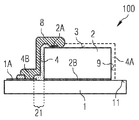
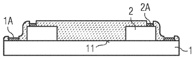
도 1은 여기에 설명된 광전 모듈(100)의 실시예를 개략적 측면도로 도시한다. 캐리어(1)는 접촉지점(1A)을 포함한다. 실장면(11) 상에 복사 방출 반도체칩(2)이 적용되어 있으며, 복사 방출 반도체칩은 전자기 복사의 생성을 위해 활성 영역을 포함한다. 또한, 복사 방출 반도체칩(2)은 제1접촉면(2A) 및 제2접촉면(2B)을 포함한다. 복사 방출 반도체칩(2)은 상기 칩의 제2접촉면(2A)을 이용하여 캐리어(1)의 실장면(11)상에 적용되며, 이 부분에서 캐리어(1)와 전기적으로 접촉되어 있다. 예컨대, 복사 방출 반도체칩(2)은 접착되거나, 땜납 물질을 이용하여 캐리어(1)와 결합하고 있다. 반도체칩(2)의 노출된 측면(9) 및 반도체칩(2)의 복사 출사면(3) 상에 부분적으로 전기 절연층(4)이 형상 맞춤 방식으로 적용된다. 또한, 전기 절연층(4)은 영역(21) 내에서 캐리어(1)의 실장면(11)을 덮어서, 전기 절연층(4)은 접촉지점(1A)과 제1접촉면(2A) 사이에서 불연속적인 부분 없이 이어진다. 전기 절연층(4)은 제1홈(4A)을 포함하고, 제1홈은 연속적으로 복사 출사면(3) 사이에서 측면(9)을 따라 캐리어(1)까지 이어진다. 제1홈(4A)은 캐리어(1) 및 제1접촉면(2A)에 의해 측 방향으로 한정된다. 복사 방출 반도체칩(2)의 복사 출사면(3)은 부분적으로 전기 절연층(4)을 포함하지 않는다. 전기 전도성 리드 구조물(8)은 제1접촉면(2A)과 캐리어(1)의 접촉 지점(1A)을 전기적으로 접촉시킨다. 본원에서 전기 전도성 리드 구조물(8)은 전기 절연층(4) 및 두 접촉면(1A, 2A)상에 인쇄되어 있다. 본원에서 전기 절연층(4)은 라미네이팅 공정을 이용하여 적용된 필름을 가리킨다. 도 1에 따른 실시예에서, 전기 절연층(4)은 세라믹 물질로 구성된다. 마찬가지로, 전기 절연층(4)이 세라믹 형광물질로 구성되고 전기 절연층(4)이 적어도 부분적으로, 복사 방출 반도체칩(2)으로부터 1차 방출된 전자기 복사로부터 다른 파장의 복사로 변환하여, 광전 모듈(100)이 혼합광을 방출하는 것을 고려할 수 있다.1 shows a schematic side view of an embodiment of the
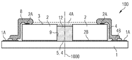
도 2는 나란히 배치된 2개의 복사 방출 반도체칩(2)을 포함한 광전 모듈(100)을 도시한다. 반도체칩(2)은 그 사이에 간극(12)을 형성하고, 상기 간극은 측 방향으로 각각 측면(9) 및 캐리어(1)에 의해 한정된다. 간극(12) 내에 절연층(5)이 배치되어 있고, 절연층은 간극(12)을 적어도 부분적으로 채우며, 측면(9) 및 캐리어(1) 상에 형상 맞춤 방식으로 적용된다. 마찬가지로, 절연층(5) 대신 또는 부가적으로, 전기 절연층(4)이 간극(12) 안에 삽입된 것을 고려할 수 있다. 제1홈(4A)은 불연속적인 부분 없이 두 반도체칩(2) 사이에 이어지며, 접촉면(2A)에 의해 측 방향으로 한정된다. 그 결과, 반도체칩들의 복사 출사면(3)은 적어도 국부적으로 노출된다. 2 shows a
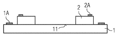
도 3a 내지 3d는 여기에 설명한 광전 모듈(100)의 실시예의 제조를 위한 개별 제조 단계를 도시한다. 이를 위해, 우선, 도 3a에 도시된 바와 같이, 캐리어(1)가 제공되고, 캐리어(1)의 실장면(11) 상에 반도체칩(2)이 적용된다.3A-3D show individual manufacturing steps for the fabrication of an embodiment of the
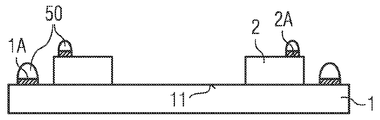
추가적인 단계에서, 도 3b에 도시된 바와 같이, 캐리어(1)의 접촉면(1A) 및 반도체칩(2)의 접촉면(2A)은 래커(50)로 덮인다. 또는, 접촉면은 필름, 밀랍 또는 다른 부착층으로 덮일 수 있다. In a further step, as shown in FIG. 3B, the
도 3c에 따르면, 부가적 단계에서 광전 모듈(100)의 노출된 외부면 상에 전기 절연층(4)의 물질이 적용되어, 측면(9) 및 복사 출사면(3)은 적어도 국부적으로 전기 절연층(4)으로 덮인다. 상기 적용은 예컨대 소결 공정 또는 몰딩 공정을 이용하여 실시할 수 있다. 마찬가지로, 전기 절연층(4)이 라미네이팅 공정 또는 분사 공정을 이용하여 적용되는 것도 고려할 수 있다. According to FIG. 3c, in an additional step a material of the
또한, 전기 절연층(4)의 물질은 선택적 증착을 이용하여, 예컨대 플라즈마 공정, 플라즈마 스프레이 공정을 이용하여 또는 스퍼터링을 이용하여 적용될 수 있다.In addition, the material of the electrically insulating
추가적인 단계에서 도 3d에서는 물리적 및/또는 기계적 물질 제거를 이용하여 래커(50)가 제거되어, 적어도 접촉면(1A, 2A)이 노출된다. In an additional step, in FIG. 3D the
복사 출사면(3)은 전기 절연층(4)의 물질에 의해, 접촉면(2A)이 연장된 지점들을 제외하고 완전히 덮여 있으며, 본원에서 전기 절연층(4)은 복사 투과성 세라믹을 포함하여 형성되거나 세라믹 형광물질로 구성된다. The
최종 단계에서, 반도체칩(2)이 전기 전도성 리드 구조물(8)을 지나 접촉 지점(1A, 2A)의 자리에 접촉되는 것을 실시할 수 있다. In the final step, the
또는, 전기 절연층(4)이 사전 구조화된 마스크를 사용하여 적용될 수 있다. 예컨대, 전기 절연층(4)은 분사 공정에 의해, 예컨대 플라즈마 증착을 이용하여 적용될 수 있다.Alternatively, the
본 발명은 실시예에 따른 설명에 의하여 제한되지 않는다. 오히려 본 발명은 각각의 새로운 특징 및 특징들의 각 조합을 포함하고, 이러한 점은 특히, 상기 특징 또는 상기 조합이 그 자체로 명백하게 특허청구범위 또는 실시예에서 제공되지 않더라도, 특허청구범위에서의 특징들의 각 조합을 포괄한다.The present invention is not limited by the description according to the embodiment. Rather, the invention includes each new feature and each combination of features, which in particular is a feature of the features in the claims, even if the feature or the combination is not explicitly provided by itself in the claims or the examples. Cover each combination.
Claims (12)
제1접촉면(2A) 및 제2접촉면(2B)을 갖는 복사 방출 반도체칩(2);
제1홈(4A) 및 제2홈(4B)을 갖는 전기 절연층(4); 및
적어도 하나의 전기 전도성 리드 구조물(8)을 포함하고,
상기 제1접촉면(2A)은 캐리어(1) 반대편의 복사 방출 반도체칩(2)의 측에 배치되고,
상기 전기 절연층(4)은, 적어도 국부적으로 상기 캐리어(1) 및 반도체칩(2) 상에 적용되며, 제1접촉면(2A)의 영역에 제1홈(4A)을 포함하며, 접촉지점(1A)의 영역에 제2홈(4B)을 포함하고,
상기 전기 전도성 리드 구조물(8)은 전기 절연층(4) 상에 배치되고,
상기 제1접촉면(2A)은 상기 캐리어(1)의 접촉지점(1A)과 전기적으로 접촉하고,
상기 전기 절연층(4)은 주로 세라믹 물질로 형성되는 것을 특징으로 하는 광전 모듈(100).A carrier 1 having at least one contact point 1A;
A radiation emitting semiconductor chip 2 having a first contact surface 2A and a second contact surface 2B;
An electrical insulation layer 4 having a first groove 4A and a second groove 4B; And
At least one electrically conductive lead structure 8,
The first contact surface 2A is disposed on the side of the radiation emitting semiconductor chip 2 opposite the carrier 1,
The electrically insulating layer 4 is applied at least locally on the carrier 1 and the semiconductor chip 2 and includes a first groove 4A in the region of the first contact surface 2A, and includes a contact point ( The second groove 4B in the region of 1A,
The electrically conductive lead structure 8 is disposed on the electrically insulating layer 4,
The first contact surface 2A is in electrical contact with the contact point 1A of the carrier 1,
The electrical insulation layer (4) is characterized in that the predominantly formed of a ceramic material.
상기 광전 모듈은 적어도 2개의 복사 방출 반도체칩(2)을 포함하고,
상기 전기 절연층(4)은 국부적으로 상기 복사 방출 반도체칩(2) 사이에 배치되는 것을 특징으로 하는 광전 모듈(100).The method of claim 1,
The photovoltaic module comprises at least two radiation emitting semiconductor chips 2,
The electrical insulation layer (4) is arranged locally between the radiation emitting semiconductor chips (2).
상기 전기 절연층(4)은 홈들(4A, 4B)을 제외하고 상기 광전 모듈(100)의 노출된 외부면 상에 형상 맞춤 방식으로 적용되는 것을 특징으로 하는 광전 모듈(100).The method according to claim 1 or 2,
The electrical insulation layer (4), characterized in that the electrical insulation layer (4) is applied in a shape-fitting manner on the exposed outer surface of the photoelectric module (100) except for the grooves (4A, 4B).
상기 전기 절연층(4)은 복사 투과성이며, 상기 반도체칩(2)의 복사 출사면(3)을 국부적으로 덮는 것을 특징으로 하는 광전 모듈(100).The method according to any one of claims 1 to 3,
The electrical insulation layer (4) is characterized in that it is radiation transmissive and covers the radiation exit surface (3) of the semiconductor chip (2) locally.
상기 전기 절연층(4)은 세라믹 형광물질로 구성되는 것을 특징으로 하는 광전 모듈(100).The method according to any one of claims 1 to 4,
The electrical insulation layer (4) is characterized in that consisting of a ceramic fluorescent material.
상기 제1홈(4A)은 상기 전기 절연층(4) 내에서 상기 반도체칩(2)의 복사 출사면(3)과 캐리어(1) 사이에서 상기 반도체칩(2)의 측면(9)을 따라 연속적으로 이어지며, 측 방향으로 상기 제1접촉면(2A) 및 캐리어(1)에 의해 한정되는 것을 특징으로 하는 광전 모듈(100).6. The method according to any one of claims 1 to 5,
The first groove 4A is along the side surface 9 of the semiconductor chip 2 between the radiation exit surface 3 of the semiconductor chip 2 and the carrier 1 in the electrical insulation layer 4. A photovoltaic module (100) characterized by being continuously connected and defined by the first contact surface (2A) and the carrier (1) in the lateral direction.
상기 제1홈(4A)은 상기 전기 절연층(4) 내에서 인접한 반도체칩(2) 사이에서 연속적으로 이어지며, 측 방향으로 접촉면(2A)에 의해 한정되는 것을 특징으로 하는 광전 모듈(100).7. The method according to any one of claims 1 to 6,
The first groove 4A extends continuously between adjacent semiconductor chips 2 in the electrical insulation layer 4, and is defined by the contact surface 2A in the lateral direction. .
상기 반도체칩(2) 사이에 절연층(5)이 배치되는 것을 특징으로 하는 광전 모듈(100).The method according to any one of claims 1 to 7,
Optoelectronic module (100), characterized in that the insulating layer (5) is disposed between the semiconductor chip (2).
상기 전기 절연층(4)은 필름인 것을 특징으로 하는 광전 모듈(100).The method according to any one of claims 1 to 8,
Optoelectronic module (100), characterized in that the electrical insulation layer (4) is a film.
상기 전기 절연층(4)은 라미네이팅 공정을 이용하여 적용되는 것을 특징으로 하는 광전 모듈(100).The method of claim 9,
The electrical insulation layer (4) is characterized in that it is applied using a laminating process.
상기 전기 절연층(4)은 소결 공정을 이용하여 적용되는 것을 특징으로 하는 광전 모듈(100).The method according to any one of claims 1 to 8,
The electrical insulation layer (4) is characterized in that it is applied using a sintering process.
상기 전기 절연층(4)은 몰딩 공정을 이용하여 적용되는 것을 특징으로 하는 광전 모듈(100).The method according to any one of claims 1 to 8,
The electrical insulation layer (4) is characterized in that it is applied using a molding process.
Applications Claiming Priority (2)
| Application Number | Priority Date | Filing Date | Title |
|---|---|---|---|
| DE102009042205A DE102009042205A1 (en) | 2009-09-18 | 2009-09-18 | Optoelectronic module |
| DE102009042205.6 | 2009-09-18 |
Publications (1)
| Publication Number | Publication Date |
|---|---|
| KR20120080608A true KR20120080608A (en) | 2012-07-17 |
Family
ID=43333046
Family Applications (1)
| Application Number | Title | Priority Date | Filing Date |
|---|---|---|---|
| KR1020127009750A KR20120080608A (en) | 2009-09-18 | 2010-09-06 | Optoelectronic module |
Country Status (8)
| Country | Link |
|---|---|
| US (1) | US20120228666A1 (en) |
| EP (1) | EP2478557A1 (en) |
| JP (1) | JP2013505561A (en) |
| KR (1) | KR20120080608A (en) |
| CN (1) | CN102576707A (en) |
| DE (1) | DE102009042205A1 (en) |
| TW (1) | TW201117439A (en) |
| WO (1) | WO2011032853A1 (en) |
Families Citing this family (8)
| Publication number | Priority date | Publication date | Assignee | Title |
|---|---|---|---|---|
| DE102011016935A1 (en) * | 2011-04-13 | 2012-10-18 | Osram Opto Semiconductors Gmbh | A method of manufacturing a semiconductor light emitting device and light emitting semiconductor device |
| DE102011079708B4 (en) | 2011-07-25 | 2022-08-11 | Osram Gmbh | SUPPORT DEVICE, ELECTRICAL DEVICE WITH SUPPORT DEVICE, AND METHOD FOR MANUFACTURING SAME |
| DE102012101889A1 (en) | 2012-03-06 | 2013-09-12 | Osram Opto Semiconductors Gmbh | Method for producing an optoelectronic semiconductor chip and optoelectronic semiconductor chip |
| DE102012108160A1 (en) * | 2012-09-03 | 2014-03-06 | Osram Opto Semiconductors Gmbh | Optoelectronic semiconductor component and method for producing an optoelectronic semiconductor component |
| JP6430630B2 (en) * | 2014-09-02 | 2018-11-28 | フィリップス ライティング ホールディング ビー ヴィ | Method for applying illumination devices to surfaces and illumination surfaces |
| DE102015104886A1 (en) * | 2015-03-30 | 2016-10-06 | Osram Opto Semiconductors Gmbh | Optoelectronic semiconductor chip, optoelectronic semiconductor component and method for producing an optoelectronic semiconductor chip |
| CN108700275B (en) * | 2016-02-24 | 2022-05-31 | 奇跃公司 | Low profile interconnect for light emitter |
| DE102019219016A1 (en) * | 2019-12-05 | 2021-06-10 | OSRAM Opto Semiconductors Gesellschaft mit beschränkter Haftung | OPTOELECTRONIC DEVICE AND METHOD OF MANUFACTURING AN OPTOELECTRONIC DEVICE |
Family Cites Families (16)
| Publication number | Priority date | Publication date | Assignee | Title |
|---|---|---|---|---|
| JPH0518839U (en) * | 1991-08-30 | 1993-03-09 | シヤープ株式会社 | Light emitting device |
| DE10308866A1 (en) * | 2003-02-28 | 2004-09-09 | Osram Opto Semiconductors Gmbh | Lighting module and method for its production |
| DE10353679A1 (en) * | 2003-11-17 | 2005-06-02 | Siemens Ag | Cost-effective, miniaturized assembly and connection technology for LEDs and other optoelectronic modules |
| US7361938B2 (en) * | 2004-06-03 | 2008-04-22 | Philips Lumileds Lighting Company Llc | Luminescent ceramic for a light emitting device |
| DE102004050371A1 (en) * | 2004-09-30 | 2006-04-13 | Osram Opto Semiconductors Gmbh | Optoelectronic component with a wireless contact |
| US20060154393A1 (en) * | 2005-01-11 | 2006-07-13 | Doan Trung T | Systems and methods for removing operating heat from a light emitting diode |
| EP1922764A1 (en) * | 2005-08-24 | 2008-05-21 | Philips Intellectual Property & Standards GmbH | Light emitting diodes and lasers diodes with color converters |
| DE102005041099A1 (en) * | 2005-08-30 | 2007-03-29 | Osram Opto Semiconductors Gmbh | LED chip with glass coating and planar assembly and connection technology |
| JP2007158262A (en) * | 2005-12-08 | 2007-06-21 | Rohm Co Ltd | Method of manufacturing semiconductor light-emitting element |
| US20070241661A1 (en) * | 2006-04-12 | 2007-10-18 | Yin Chua B | High light output lamps having a phosphor embedded glass/ceramic layer |
| DE102007021009A1 (en) * | 2006-09-27 | 2008-04-10 | Osram Opto Semiconductors Gmbh | Light-emitting diode arrangement and method for producing such |
| US9024349B2 (en) * | 2007-01-22 | 2015-05-05 | Cree, Inc. | Wafer level phosphor coating method and devices fabricated utilizing method |
| DE102007011123A1 (en) * | 2007-03-07 | 2008-09-11 | Osram Opto Semiconductors Gmbh | Light-emitting module and method of manufacturing a light-emitting module |
| JP2008244357A (en) * | 2007-03-28 | 2008-10-09 | Toshiba Corp | Semiconductor light-emitting device |
| DE102007046337A1 (en) * | 2007-09-27 | 2009-04-02 | Osram Opto Semiconductors Gmbh | Optoelectronic semiconductor chip, optoelectronic component and method for producing an optoelectronic component |
| DE102008019902A1 (en) * | 2007-12-21 | 2009-06-25 | Osram Opto Semiconductors Gmbh | Optoelectronic component and production method for an optoelectronic component |
-
2009
- 2009-09-18 DE DE102009042205A patent/DE102009042205A1/en not_active Withdrawn
-
2010
- 2010-09-06 US US13/496,805 patent/US20120228666A1/en not_active Abandoned
- 2010-09-06 KR KR1020127009750A patent/KR20120080608A/en not_active Application Discontinuation
- 2010-09-06 EP EP10752334A patent/EP2478557A1/en not_active Withdrawn
- 2010-09-06 CN CN2010800416619A patent/CN102576707A/en active Pending
- 2010-09-06 JP JP2012529207A patent/JP2013505561A/en active Pending
- 2010-09-06 WO PCT/EP2010/063035 patent/WO2011032853A1/en active Application Filing
- 2010-09-09 TW TW099130463A patent/TW201117439A/en unknown
Also Published As
| Publication number | Publication date |
|---|---|
| EP2478557A1 (en) | 2012-07-25 |
| TW201117439A (en) | 2011-05-16 |
| JP2013505561A (en) | 2013-02-14 |
| US20120228666A1 (en) | 2012-09-13 |
| DE102009042205A1 (en) | 2011-03-31 |
| WO2011032853A1 (en) | 2011-03-24 |
| CN102576707A (en) | 2012-07-11 |
Similar Documents
| Publication | Publication Date | Title |
|---|---|---|
| KR20120080608A (en) | Optoelectronic module | |
| JP5628425B2 (en) | Semiconductor component and method for manufacturing semiconductor component | |
| JP6099764B2 (en) | Method for manufacturing optoelectronic semiconductor components and optoelectronic semiconductor components | |
| US7695990B2 (en) | Fabricating surface mountable semiconductor components with leadframe strips | |
| TWI389328B (en) | Optoelectronic semiconductor component and method for manufacturing an optoelectronic semiconductor component | |
| TWI446593B (en) | Method for manufacturing an optoelectronic semiconductor component and said optoelectronic semiconductor component | |
| CN106663659B (en) | Surface mountable semiconductor device and method of manufacturing the same | |
| US20070018191A1 (en) | Side view LED with improved arrangement of protection device | |
| JP5670571B2 (en) | Method for manufacturing at least one optoelectronic semiconductor component | |
| KR20100074100A (en) | Optoelectronic semiconductor chip, optoelectronic component, and method for producing an optoelectronic component | |
| KR101509045B1 (en) | Led package and method of manufacturing same | |
| US9190553B2 (en) | Optoelectronic semiconductor component, method for producing same and use of such a component | |
| US20160190410A1 (en) | Optoelectronic component and method for the production thereof | |
| KR102527885B1 (en) | Method for manufacturing a connected carrier, a connected carrier and an optoelectronic semiconductor component with a connected carrier | |
| KR20110057263A (en) | Optoelectronic module having a carrier substrate and a plurality of radiation-emitting semiconductor components and method for the production thereof | |
| US20160155891A1 (en) | Optoelectronic component and method for the production thereof | |
| US9935250B2 (en) | Optoelectronic component and method of production thereof | |
| JP2018514950A (en) | Method for creating optoelectronic component and surface mountable optoelectronic component | |
| CN100530714C (en) | Electrooptical device with wireless contaction | |
| KR20130062985A (en) | Radiation-emitting component and method for producing a radiation-emitting component | |
| US11189990B2 (en) | Semiconductor laser component and method of producing a semiconductor laser component | |
| KR101457827B1 (en) | Method for producing an optoelectronic semiconductor component | |
| US8847247B2 (en) | Optoelectronic module comprising at least one first semiconductor body having a radiation outlet side and an insulation layer and method for the production thereof | |
| US9876155B2 (en) | Optoelectronic component and method for the production thereof | |
| KR101533068B1 (en) | PCB and Semiconductor module including the same |
Legal Events
| Date | Code | Title | Description |
|---|---|---|---|
| WITN | Application deemed withdrawn, e.g. because no request for examination was filed or no examination fee was paid |