KR20120040756A - Process for metallic contamination reduction in silicon wafers - Google Patents
Process for metallic contamination reduction in silicon wafers Download PDFInfo
- Publication number
- KR20120040756A KR20120040756A KR1020127009189A KR20127009189A KR20120040756A KR 20120040756 A KR20120040756 A KR 20120040756A KR 1020127009189 A KR1020127009189 A KR 1020127009189A KR 20127009189 A KR20127009189 A KR 20127009189A KR 20120040756 A KR20120040756 A KR 20120040756A
- Authority
- KR
- South Korea
- Prior art keywords
- silicon wafer
- wafers
- silicon
- wafer
- copper
- Prior art date
Links
Images

Classifications
-
- H—ELECTRICITY
- H01—ELECTRIC ELEMENTS
- H01L—SEMICONDUCTOR DEVICES NOT COVERED BY CLASS H10
- H01L21/00—Processes or apparatus adapted for the manufacture or treatment of semiconductor or solid state devices or of parts thereof
- H01L21/02—Manufacture or treatment of semiconductor devices or of parts thereof
- H01L21/04—Manufacture or treatment of semiconductor devices or of parts thereof the devices having at least one potential-jump barrier or surface barrier, e.g. PN junction, depletion layer or carrier concentration layer
- H01L21/18—Manufacture or treatment of semiconductor devices or of parts thereof the devices having at least one potential-jump barrier or surface barrier, e.g. PN junction, depletion layer or carrier concentration layer the devices having semiconductor bodies comprising elements of Group IV of the Periodic System or AIIIBV compounds with or without impurities, e.g. doping materials
- H01L21/30—Treatment of semiconductor bodies using processes or apparatus not provided for in groups H01L21/20 - H01L21/26
- H01L21/322—Treatment of semiconductor bodies using processes or apparatus not provided for in groups H01L21/20 - H01L21/26 to modify their internal properties, e.g. to produce internal imperfections
- H01L21/3221—Treatment of semiconductor bodies using processes or apparatus not provided for in groups H01L21/20 - H01L21/26 to modify their internal properties, e.g. to produce internal imperfections of silicon bodies, e.g. for gettering
- H01L21/3225—Thermally inducing defects using oxygen present in the silicon body for intrinsic gettering
-
- H—ELECTRICITY
- H01—ELECTRIC ELEMENTS
- H01L—SEMICONDUCTOR DEVICES NOT COVERED BY CLASS H10
- H01L21/00—Processes or apparatus adapted for the manufacture or treatment of semiconductor or solid state devices or of parts thereof
- H01L21/02—Manufacture or treatment of semiconductor devices or of parts thereof
- H01L21/04—Manufacture or treatment of semiconductor devices or of parts thereof the devices having at least one potential-jump barrier or surface barrier, e.g. PN junction, depletion layer or carrier concentration layer
- H01L21/18—Manufacture or treatment of semiconductor devices or of parts thereof the devices having at least one potential-jump barrier or surface barrier, e.g. PN junction, depletion layer or carrier concentration layer the devices having semiconductor bodies comprising elements of Group IV of the Periodic System or AIIIBV compounds with or without impurities, e.g. doping materials
- H01L21/30—Treatment of semiconductor bodies using processes or apparatus not provided for in groups H01L21/20 - H01L21/26
- H01L21/324—Thermal treatment for modifying the properties of semiconductor bodies, e.g. annealing, sintering
Landscapes
- Engineering & Computer Science (AREA)
- Physics & Mathematics (AREA)
- Condensed Matter Physics & Semiconductors (AREA)
- General Physics & Mathematics (AREA)
- Manufacturing & Machinery (AREA)
- Computer Hardware Design (AREA)
- Microelectronics & Electronic Packaging (AREA)
- Power Engineering (AREA)
- Crystals, And After-Treatments Of Crystals (AREA)
- Cleaning Or Drying Semiconductors (AREA)
Abstract
표면 및 내부를 갖는 실리콘 웨이퍼로부터 구리, 니켈 및 그들의 조합으로부터 선택된 오염물을 제거하기 위한 공정으로서, 산화 개시 온도 또는 그 위의 온도로부터 제어된 분위기 내의 실리콘 웨이퍼를 냉각시키는 단계 및 상기 산화 개시 온도에서 산소를 포함하는 분위기의 흐름을 개시하여 실리콘 웨이퍼 표면 주위에 산화 환경을 생성함으로써, 실리콘 웨이퍼 표면 상에 산화물층을 형성하고 산화물층과 실리콘 웨이퍼 내부 사이의 계면에 변형층을 형성하는 단계를 포함한다. 웨이퍼를 냉각시키는 단계는, 또한 실리콘 웨이퍼 내부로부터 변형층으로 오염물의 원자들이 확산할 수 있도록 제어된다. 그 후, 실리콘 웨이퍼를 세정하여 산화물층 및 변형층을 제거함으로써 변형층으로 확산된 상기 오염물을 제거한다.A process for removing selected contaminants from copper, nickel and combinations thereof from a silicon wafer having a surface and an interior, the method comprising: cooling a silicon wafer in a controlled atmosphere from an oxidation onset temperature or above and oxygen at the oxidation onset temperature Initiating the flow of the atmosphere to create an oxidizing environment around the silicon wafer surface, thereby forming an oxide layer on the silicon wafer surface and forming a strained layer at the interface between the oxide layer and the inside of the silicon wafer. Cooling the wafer is also controlled to allow atoms of contaminants to diffuse from the inside of the silicon wafer into the strained layer. Thereafter, the silicon wafer is cleaned to remove the oxide layer and the strained layer to remove the contaminants diffused into the strained layer.
Description
본 발명은 일반적으로 반도체 재료 기판들의 준비에 관련되며, 특히 전자 소자들의 제조에 사용되는 실리콘 웨이퍼들에 관련된다. 보다 구체적으로, 본 발명은 웨이퍼 내부 또는 벌크(bulk)로부터 구리와 같은 금속 오염물들의 농도를 줄이기 위해 하나 이상의 실리콘 웨이퍼를 열처리하거나 어닐링(annealing)하는 공정에 관련된다. 또한, 본 발명의 공정은 하나 이상의 실리콘 웨이퍼의 벌크 내 및 그 표면 상의 응집 공공(vacancy) 결함들의 크기 또는 농도를 감소시키는 방식으로 수행될 수 있다. The present invention relates generally to the preparation of semiconductor material substrates, in particular to silicon wafers used in the manufacture of electronic devices. More specifically, the present invention relates to a process of annealing or annealing one or more silicon wafers to reduce the concentration of metal contaminants, such as copper, within or from the bulk of the wafer. In addition, the process of the present invention may be carried out in a manner that reduces the size or concentration of cohesive vacancy defects in the bulk and on the surface of one or more silicon wafers.
실리콘 디바이스 성능은 금속성 오염물들에 의해 열화된다. 구리, 철 및 니켈을 포함하는 전이 금속들은 집적 회로 제조 조건들과 연관된 통상적인 열적 사이클들 동안 용해되고 확산될 수 있다. 집적 회로 제조와 연관된 온도들로부터의 냉각 동안, 구리 및 다른 금속들은 웨이퍼의 표면뿐 아니라 예를 들어 붕소(예를 들면, p형 웨이퍼 또는 영역)로 도핑된 영역들, 결함 사이트들 및 계면들에 석출되거나 집중될 수 있다. 이러한 석출물들은 일반적으로 금속 오염물과 실리콘의 반응 생성물로 여겨진다. 구리의 경우, 석출물들은 구리 실리사이드 석출물로 여겨진다. 석출물들은 종종 전위들(dislocations) 및 다른 결함들을 생성한다. 석출물들 및 그들과 연관된 전위들 및 결함들은, 웨이퍼의 디바이스 제조 영역 내에 존재하는 경우, 웨이퍼로부터 만들어진 집적 회로를 쓸모없게 한다. 또한, 구리 실리사이드 석출물들은 헤이즈 결함(haze defect)으로 불리는 것을 형성하는데, 그 이유는 일반적인 에칭 처리 및 밝은 광 검사를 할 경우, 석출물들이 웨이퍼의 표면 상에 헤이즈처럼 보이는 결함들을 유발하기 때문이다. 이러한 문제로 인해, 집적 회로 제조자들은 일반적으로, 실리콘 웨이퍼의 표면 상의 구리의 농도가, 본 분야의 표준 방법들에 의해 결정된 바와 같이 1x10¹⁰ 원자/㎠ 내지 1x10¹¹ 원자/㎠ 일 것을 요구한다. 또한, 무작위의 디바이스 오류의 큰 비율이 구리 실리사이드 석출물들로 추적될 수 있기 때문에 이러한 필요요건은 5x10⁹ 원자/㎠, 1x10⁹ 원자/㎠ 또는 그 아래의 값으로 감소될 것이다.Silicon device performance is degraded by metallic contaminants. Transition metals including copper, iron and nickel can dissolve and diffuse during typical thermal cycles associated with integrated circuit fabrication conditions. During cooling from the temperatures associated with integrated circuit fabrication, copper and other metals may be deposited on the surface of the wafer, as well as regions, defect sites and interfaces doped with, for example, boron (eg, p-type wafer or region). Can be precipitated or concentrated. These precipitates are generally regarded as reaction products of metal contaminants and silicon. In the case of copper, the precipitates are considered to be copper silicide precipitates. Precipitates often create dislocations and other defects. Precipitates and dislocations and defects associated with them render the integrated circuit made from the wafer useless when present in the device fabrication area of the wafer. In addition, copper silicide precipitates form what are called haze defects because, when subjected to normal etching and bright light inspection, the precipitates cause defects that look like haze on the surface of the wafer. Due to this problem, integrated circuit manufacturers generally require that the concentration of copper on the surface of the silicon wafer be between 1 × 10 10 atoms /
쵸크랄스키법(Czochralski method) 또는 부유띠법(floating-zone method)에 의해 생산된 단결정 실리콘 잉곳의 성장으로 시작하는 공정에 의해 단결정 실리콘 웨이퍼들이 일반적으로 제조된다. 결정 잉곳은 통상적으로 와이어 톱을 이용하여 웨이퍼들로 슬라이스되고, 웨이퍼들은 래핑(lapping)에 의해 평탄화되고 기계적 손상 및 오염을 제거하기 위해 화학적으로 에칭된다. 에칭된 후, 웨이퍼들은 한쪽 또는 양쪽으로 연마된다. COP(crystal originated particles)를 줄이기 위해 열적 어닐링과 같은 추가 처리를 웨이퍼들에 가하더라도, 그 처리는 통상적으로 최신 세정 방법들로 종료한다. 이러한 세정 이후에, 연마된 웨이퍼들의 표면 상의 구리 농도는, TXRF(total reflection spectroscopy) 측정에 의해 결정되는 바와 같이, 통상적으로 1x10¹⁰ 원자/㎠ 미만이다. 예를 들어 C. Neumann 등의 Spectrochemica Acta, 10 (1991), pp.1369-1377; 및 Ingle & Crouch의 Spectrochemical Analysis, Prentice Hall, 1988를 참조하라. 그러나, 이들 웨이퍼의 표면 구리 농도는 포화 상태에 도달할 때까지 상온에서도 시간이 지남에 따라 증가하는 경향이 있다. 따라서, 세정 직후 표면 구리 농도에 대한 목표 규격을 만족시키는 웨이퍼들도 5 내지 10달 후에는 이러한 규격을 만족시키지 못할 수 있다.Single crystal silicon wafers are generally manufactured by a process starting with the growth of single crystal silicon ingots produced by the Czochralski method or the floating-zone method. Crystal ingots are typically sliced into wafers using a wire saw, and the wafers are planarized by lapping and chemically etched to remove mechanical damage and contamination. After etching, the wafers are polished to one or both sides. Although additional processing, such as thermal annealing, is applied to the wafers to reduce crystal originated particles (COP), the processing typically ends with modern cleaning methods. After this cleaning, the copper concentration on the surface of the polished wafers is typically less than 1 × 10 10 atoms /
오늘날까지, 실리콘 웨이퍼들의 구리 오염 문제를 다루는 3가지 주요 접근법들이 존재해 왔다. 첫번째 접근법은, 연마 작업 동안 실리콘에 도입되는 구리 및 다른 금속들의 양을 줄이는 것을 포함한다. 구체적으로, 이러한 오염물들의 소스들을, 가능한 한, 식별하고 제거하는 것에 주로 초점을 맞추었다. 연마 혼합물 내의 금속량을 줄이는 것 이외에, Prigge 등(DE 3939661 A1)에 의해 개시된 것과 같은 다른 방법들은, 구리와 배위 복합물을 형성하는 소정의 시약과 연마제들을 혼합함으로써 연마하는 동안 웨이퍼에 실질적으로 포함되는 구리의 양을 제한하는 것을 포함한다. 이러한 배위 복합물은 구리가 실리콘으로 들어갈 수 있는 능력을 제한하는 특정 형태로 구리를 유지하는 역할을 한다. 연마 혼합물들을 수정하여 실리콘 웨이퍼들 내의 구리 오염의 정도를 줄이더라도, 통상적으로 다른 구리 저감 방법들에 대한 필요성을 없앨 만큼 충분히 효과적이지 않다. 또한, 집적 회로 제조에 의한 실리콘 웨이퍼들 내의 금속성 오염 수준에 대해 보다 엄격한 제한이 가해질수록 실리콘 웨이퍼들 내의 금속성 오염을 제어하기 위해 훨씬 비싼 선택인 연마 혼합물 수정에 의존하게 한다.To date, there have been three main approaches to address the problem of copper contamination of silicon wafers. The first approach involves reducing the amount of copper and other metals introduced into the silicon during the polishing operation. Specifically, the focus was primarily on identifying and eliminating these sources of contaminants. In addition to reducing the amount of metal in the polishing mixture, other methods, such as those disclosed by Prigge et al. (DE 3939661 A1), are substantially incorporated into the wafer during polishing by mixing the abrasive with certain reagents forming copper and coordination complexes. Limiting the amount of copper. This coordination composite serves to keep copper in a particular form that limits the ability of copper to enter silicon. Although modifying the polishing mixtures to reduce the degree of copper contamination in silicon wafers, it is typically not effective enough to eliminate the need for other copper abatement methods. In addition, the more stringent restrictions placed on the level of metallic contamination in silicon wafers by integrated circuit fabrication, make them rely on polishing mixture modifications, which are a much more expensive option for controlling metallic contamination in silicon wafers.
연마된 실리콘 웨이퍼들의 금속 오염을 다루는 두번째 접근법은, 구리 및 다른 금속들을 트랩하여 이러한 금속들이 웨이퍼의 디바이스 영역에 도달하지 못하게 하는 진성 게터링(intrinsic gettering)이다. 진성 게터링 기술은 웨이퍼로부터 제조되는 집적 회로들의 기능을 저해하지 않는 위치들(즉, 종종 "벌크(bulk)", "웨이퍼 벌크" 또는 "벌크 영역"으로 불리우는 디바이스 영역 아래의 웨이퍼 내부 영역)에서 결함 사이트(defect site)들을 실리콘 웨이퍼에 도입하는 것을 수반한다. 그러나, 게터링 기술들은 금속성 오염물들을 제어하는 완전히 수용가능한 해결책으로 증명되지는 않았다. 예를 들어, 실리콘에서의 구리 및 니켈과 같은 금속의 높은 확산계수로 인해 이러한 금속들은 게터링 사이트들에서 탈출하여 디바이스 영역에 도달할 수 있다. 또한, 실리콘에 게터링 싱크(gettering sink)들로서 도입된 결함들이 예를 들어 소수 캐리어 재결합 라이프타임을 줄임으로써 실리콘의 품질을 낮출 수 있다.A second approach to dealing with metal contamination of polished silicon wafers is intrinsic gettering, which traps copper and other metals to prevent these metals from reaching the device region of the wafer. Intrinsic gettering techniques are used at locations that do not interfere with the functionality of integrated circuits manufactured from a wafer (ie, an area within the wafer below the device area, often referred to as a "bulk", "wafer bulk" or "bulk area"). This involves introducing defect sites into the silicon wafer. However, gettering techniques have not proven to be a fully acceptable solution for controlling metallic contaminants. For example, high diffusion coefficients of metals such as copper and nickel in silicon can cause these metals to escape from gettering sites and reach the device region. In addition, defects introduced as gettering sinks in silicon can lower the quality of silicon, for example by reducing minority carrier recombination life time.
연마된 실리콘 웨이퍼들의 금속성 오염의 문제를 다루는 세번째 접근법은, 하나 이상의 소위 "저온 어닐링(low temperature anneals)"을 사용하여 구리를 실리콘 웨이퍼의 벌크로부터 제거될 수 있는 표면으로 몰아내는 것이다. 예를 들어, Falster 등의 미국 특허 번호 6,100,167호는 일반적으로, 웨이퍼를 상대적으로 짧은 시간 기간 동안(예를 들어, 약 5분 내지 약 1.5시간 사이) 저온 어닐링(예를 들어, 약 225 내지 약 300℃ 사이) 처리하는 것을 포함하여, 구리가 웨이퍼의 표면으로 확산하는 속도를 증가시킨다. 표면으로 확산시킨 후, 세정 작업을 수행하는 것에 의해 구리가 표면에서 제거된다. 세정하여 구리를 제거하는 것을 포함하는, 하나 이상의 이러한 저온 어닐링은, 구리 실리사이드 석출물의 형성을 피하기 위해 연마된 실리콘 웨이퍼가 500℃를 초과하는 온도로 가열되기 전에 수행될 수 있다. 이러한 저온 어닐링들이 단일 실리콘 웨이퍼로부터 효과적으로 구리를 제거하는데 사용될 수 있더라도, 처리량을 상당히 감소시키고 웨이퍼의 비용을 상당히 증가시키기 때문에 통상적인 제조 공정에서 구현되지 않았다. 이러한 이유로 인해, 이들 저온 어닐링들은 실험실 및 시험 응용들로 한정되어 왔다.A third approach to address the problem of metallic contamination of polished silicon wafers is to drive copper to a surface that can be removed from the bulk of the silicon wafer using one or more so-called "low temperature anneals". For example, US Pat. No. 6,100,167 to Falster et al. Generally describes cold annealing (eg, about 225 to about 300) a wafer for a relatively short period of time (eg, between about 5 minutes and about 1.5 hours). Increasing the rate at which copper diffuses to the surface of the wafer. After diffusion to the surface, copper is removed from the surface by performing a cleaning operation. One or more such low temperature annealing, including cleaning to remove copper, may be performed before the polished silicon wafer is heated to a temperature above 500 ° C. to avoid the formation of copper silicide precipitates. Although such low temperature annealing can be used to effectively remove copper from a single silicon wafer, it has not been implemented in conventional manufacturing processes because it significantly reduces throughput and significantly increases the cost of the wafer. For this reason, these low temperature anneals have been limited to laboratory and test applications.
요약하면, 실리콘 웨이퍼들의 제조는, 웨이퍼 연마와 같은 금속성 오염물들의 도입에 대한 잠재적인 요인들이 되는 많은 단계들을 포함한다. 금속성 오염을 방해하거나 또는 제거하기 위한 앞선 방법들의 단점을 고려하면, 해로운 석출물들을 형성하지 않고 종래의 제조 공정들에 포함될 수 있는, 연마된 실리콘 웨이퍼들로부터 금속성 오염물들을 제거하기 위한, 간단하고, 저비용이며 효과적인 방법에 대한 필요성이 계속 존재한다.In summary, the manufacture of silicon wafers includes many steps that are potential factors for the introduction of metallic contaminants such as wafer polishing. Given the shortcomings of the foregoing methods for obstructing or removing metallic contamination, a simple, low cost for removing metallic contaminants from polished silicon wafers, which can be included in conventional manufacturing processes without forming harmful precipitates And there is a continuing need for effective methods.
따라서, 간단히 말하면, 본 발명은 구리, 니켈 및 그들의 조합으로부터 선택된 오염물을, 실리콘 웨이퍼 표면 및 실리콘 웨이퍼 내부를 갖는 실리콘 웨이퍼로부터 제거하는 공정에 관한 것이다. 이 공정은, 산화 개시 온도 또는 그 위의 온도로부터 제어된 분위기 내에서 실리콘 웨이퍼를 냉각시키는 단계를 포함한다. 상기 산화 개시 온도에서, 실리콘 웨이퍼 표면 주위에 산화 환경을 생성하도록 산소를 포함하는 분위기의 흐름이 시작되어, 실리콘 웨이퍼 표면 상의 산화물층 및 산화물층과 실리콘 웨이퍼 내부 사이의 계면에서의 변형층(strain layer)을 형성한다. 실리콘 웨이퍼 내부로부터 변형층으로 오염물의 원자들이 확산되도록 실리콘 웨이퍼의 냉각이 제어된다. 그 후, 웨이퍼가 세정되어 산화물층 및 변형층을 제거하여, 변형층으로 확산된 상기 오염물을 제거한다.Thus, in short, the present invention relates to a process for removing contaminants selected from copper, nickel and combinations thereof from a silicon wafer having a silicon wafer surface and a silicon wafer interior. This process includes cooling the silicon wafer in an atmosphere controlled from the temperature at or above the oxidation start temperature. At the oxidation start temperature, a flow of atmosphere containing oxygen is initiated to create an oxidizing environment around the silicon wafer surface, resulting in an oxide layer on the silicon wafer surface and a strain layer at the interface between the oxide layer and the inside of the silicon wafer. ). Cooling of the silicon wafer is controlled such that atoms of contaminants diffuse from the inside of the silicon wafer into the strained layer. Thereafter, the wafer is cleaned to remove the oxide layer and the strained layer to remove the contaminants diffused into the strained layer.
또한, 본 발명은 실리콘 웨이퍼 표면 및 실리콘 웨이퍼 내부를 갖는 실리콘 웨이퍼로부터, 구리 및 니켈 중에서 선택된 오염물을 제거하는 또 다른 공정에 관한 것이다. 이 공정은 적어도 약 1100℃의 온도로 실리콘 웨이퍼를 가열하는 단계, 및 수소, 헬륨, 네온, 아르곤, 크립톤, 제논 및 그 혼합물들을 포함하는 그룹으로부터 선택된 것을 포함하는 세정 환경에 실리콘 웨이퍼 표면을 노출시켜 실리콘 웨이퍼 표면으로부터 실리콘 산화물을 제거함으로써 탈산화된(deoxidized) 실리콘 웨이퍼를 형성하는 단계를 포함한다. 탈산화된 실리콘 웨이퍼가 산화 환경에 노출되어 실리콘 웨이퍼 표면 상에 산화물층을 형성함으로써, 산화물층과 실리콘 웨이퍼 내부 사이의 계면에 변형층을 갖는 산화된 실리콘 웨이퍼를 만든다. 산화된 실리콘 웨이퍼의 온도는 실리콘 웨이퍼 내부로부터 변형층으로 오염물이 확산하도록 제어된다. 그 후, 실리콘 웨이퍼가 세정되어 실리콘 웨이퍼로부터 변형층으로 확산된 오염물을 제거함으로써 세정된 실리콘 웨이퍼를 만든다.The invention also relates to another process for removing contaminants selected from copper and nickel from a silicon wafer having a silicon wafer surface and a silicon wafer interior. This process exposes the silicon wafer surface to a cleaning environment comprising heating the silicon wafer to a temperature of at least about 1100 ° C. and a cleaning environment comprising one selected from the group comprising hydrogen, helium, neon, argon, krypton, xenon and mixtures thereof. Removing the silicon oxide from the silicon wafer surface to form a deoxidized silicon wafer. The deoxidized silicon wafer is exposed to an oxidizing environment to form an oxide layer on the silicon wafer surface, resulting in an oxidized silicon wafer having a strained layer at the interface between the oxide layer and the inside of the silicon wafer. The temperature of the oxidized silicon wafer is controlled to diffuse contaminants from inside the silicon wafer into the strained layer. Thereafter, the silicon wafer is cleaned to remove the contaminants diffused from the silicon wafer into the strained layer to form a cleaned silicon wafer.
또한, 본 발명은 실리콘 웨이퍼 표면들 및 실리콘 웨이퍼 내부들을 갖는 다수의 실리콘 웨이퍼로부터, 구리, 니켈 및 그들의 조합으로부터 선택된 오염물을 제거하는 공정에 관한 것이다. 이 공정은 약 800℃ 미만의 산화 개시 온도 또는 그 위의 온도로부터 실리콘 웨이퍼들을 냉각시키는 단계를 포함한다. 상기 산화 개시 온도에서, 실리콘 웨이퍼 표면들 주위에 산화 환경을 생성하도록 산소를 포함하는 분위기의 흐름이 개시되어, 실리콘 웨이퍼 표면들 상에 약 5 내지 약 20Å 사이의 두께를 갖는 산화물층들을 형성하고 산화물층들과 실리콘 웨이퍼 내부들 사이의 계면들에 변형층들을 형성한다. 웨이퍼들의 냉각은, 실리콘 웨이퍼 내부들로부터 변형층들로 오염물의 원자들이 확산되도록 제어된다. 그 후, 실리콘 웨이퍼들이 세정되어 산화물층들 및 변형층들을 제거함으로써, 변형층들로 확산된 상기 오염물을 제거한다.The invention also relates to a process for removing selected contaminants from copper, nickel and combinations thereof from a plurality of silicon wafers having silicon wafer surfaces and silicon wafer interiors. This process includes cooling the silicon wafers from an oxidation initiation temperature of less than about 800 ° C. or above. At the oxidation initiation temperature, a flow of an atmosphere comprising oxygen is initiated to create an oxidizing environment around the silicon wafer surfaces to form oxide layers having a thickness of between about 5 and about 20 microns on the silicon wafer surfaces. Strain layers are formed at the interfaces between the layers and the silicon wafer interiors. Cooling of the wafers is controlled to diffuse atoms of contaminants from the silicon wafer interiors into the strained layers. The silicon wafers are then cleaned to remove oxide layers and strained layers, thereby removing the contaminants diffused into the strained layers.
또한, 본 발명은 구리, 니켈 및 그들의 조합으로부터 선택된 오염물을, 실리콘 웨이퍼 표면 및 실리콘 웨이퍼 내부를 갖는 실리콘 웨이퍼로부터 제거하는 공정에 관한 것이다. 이 공정은 실리콘 웨이퍼를 아르곤을 포함하는 가열-냉각 환경에 노출시키면서 적어도 약 1100℃인 어닐링 온도로 실리콘 웨이퍼의 온도를 증가시키는 단계를 포함한다. 실리콘 웨이퍼가 어닐링 온도에 있을 때 수소, 헬륨, 네온, 아르곤, 크립톤, 제논 및 그들의 조합을 포함하는 그룹으로부터 선택된 어닐링 환경에 약 30분 내지 약 90분 사이에 있는 기간 동안 실리콘 웨이퍼를 노출시킴으로써 실리콘 웨이퍼가 어닐링되어, 실리콘 웨이퍼 표면으로부터 실리콘 산화물을 제거하고 실리콘 웨이퍼 표면에서의 노출된 응집 공공 결함들로의 실리콘 원자들의 이동을 용이하게 하여 노출된 응집 공공 결함들의 크기를 감소시킨다. 실리콘 웨이퍼를 가열-냉각 환경에 노출하는 동안 실리콘 웨이퍼의 온도가 어닐링 온도로부터 약 800℃ 이하인 산화 개시 온도로 감소된다. 웨이퍼의 온도가 산화 개시 온도로부터 감소됨에 따라, 실리콘 웨이퍼는 약 10 내지 약 100ppm 사이에 있는 농도의 산소를 포함하는 산화 환경에 노출되어, 실리콘 웨이퍼 표면 상에 산화물층을 형성하고 산화물층과 실리콘 웨이퍼 내부 사이의 계면에 변형층을 형성한다. 실리콘 웨이퍼의 온도 감소는 실리콘 웨이퍼 내부로부터 변형층으로의 오염물의 원자들의 확산을 허용하도록 제어된다. 실리콘 웨이퍼가 세정되어 실리콘 웨이퍼로부터 변형층으로 확산된 오염물을 제거한다.The invention also relates to a process for removing contaminants selected from copper, nickel and combinations thereof from a silicon wafer having a silicon wafer surface and a silicon wafer interior. The process includes increasing the temperature of the silicon wafer to an annealing temperature of at least about 1100 ° C. while exposing the silicon wafer to a heat-cooling environment comprising argon. Silicon wafer by exposing the silicon wafer for a period of between about 30 minutes and about 90 minutes to an annealing environment selected from the group comprising hydrogen, helium, neon, argon, krypton, xenon and combinations thereof when the silicon wafer is at the annealing temperature Is annealed to remove silicon oxide from the silicon wafer surface and to facilitate the migration of silicon atoms to the exposed agglomeration void defects on the silicon wafer surface to reduce the size of the exposed agglomeration void defects. While exposing the silicon wafer to a heat-cooling environment, the temperature of the silicon wafer is reduced from the annealing temperature to an oxidation initiation temperature of about 800 ° C. or less. As the temperature of the wafer decreases from the onset of oxidation, the silicon wafer is exposed to an oxidizing environment containing oxygen at a concentration between about 10 and about 100 ppm, forming an oxide layer on the silicon wafer surface and forming the oxide layer and the silicon wafer. A strained layer is formed at the interface between the interiors. The temperature reduction of the silicon wafer is controlled to allow diffusion of atoms of contaminants from inside the silicon wafer into the strained layer. The silicon wafer is cleaned to remove contaminants that have diffused from the silicon wafer into the strained layer.
본 발명의 다른 특징들 및 이점들은 다음의 상세한 설명 및 첨부 도면(들)로부터 보다 명백하게 될 것이다.Other features and advantages of the present invention will become more apparent from the following detailed description and the accompanying drawing (s).
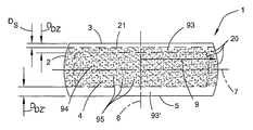
도 1은 본 발명에 따라 생산된 단결정 실리콘 웨이퍼의 구조를 나타낸다.
도 2는 본 발명에 따라 준비될 수 있는 웨이퍼의 산소 석출물 프로파일을 나타낸다.1 shows the structure of a single crystal silicon wafer produced according to the present invention.
2 shows an oxygen precipitate profile of a wafer that can be prepared in accordance with the present invention.
다음의 설명은 실리콘 내의 구리 오염에 초점이 맞추어지며, 구리가 가장 많이 연구되어지고 통상적으로 금속성 오염물들 중 가장 많이 문제가 된다. 그러나, 구리에 대해 설명된 방법들은 실리콘 내에 발견된 다른 금속성 오염물들(예를 들어, 니켈, 철, 알루미늄, 크롬 등)에도 응용가능하다.The following discussion focuses on copper contamination in silicon, with copper being the most studied and typically the most problematic of metallic contaminants. However, the methods described for copper are also applicable to other metallic contaminants found in silicon (eg nickel, iron, aluminum, chromium, etc.).
임의의 특정 이론에 구속되지 않는다고 할 때, 구리가 붕소와 함께 소정의 종류의 복합체를 형성하고, 붕소로 도핑된 실리콘 웨이퍼들에 이러한 형태로 포함되거나 "저장되는" 것으로 여겨진다. 또한, 이러한 구리-붕소 복합체들은 심지어 상온에서도 불안정한 것으로 여겨진다. 따라서, 시간이 경과함에 따라, 이러한 복합체들의 해리로 인해 구리는 인터스티셜 위치(interstitial position)를 취할 수 있다. 구리는 실리콘에서 빠른 확산자이다; 모든 금속 중에서 가장 빠르고 상온에서도 매우 유동적이다. 그러나 이외에도, 실리콘 내의 그의 용해도는 매우 온도 의존적이고 저온에서 예를 들어 상온에서 매우 낮다. 따라서, 저온에서 인터스티셜 구리는 웨이퍼의 표면을 빠르게 확산한다. 이렇듯, 웨이퍼의 표면 상의 구리의 농도는, 소정의 표면 농도 한계(예를 들어, 포화 한계)에 도달될 때까지 시간에 따라 증가하는 경향이 있다. 시간에 의존적인 것 이외에, 표면으로의 구리의 확산은 부분적으로, 연마 공정에 의해 웨이퍼에 제공되는 구리의 양 및/또는 노(furnace) 부품들 및 부속설비에 포함되는 탄소 및 실리콘 탄화물과 같은 다른 소스들의 양에 의존한다. 또한, 구리 확산도는 부분적으로 웨이퍼 내의 붕소의 농도에 의존적이다. 구체적으로, 웨이퍼의 붕소 농도가 증가함에 따라, 구리에 대한 "저장" 용량이 증가하고, 이처럼 웨이퍼 표면 상의 구리 농도의 시간에 따른 증가에 대한 잠재성이 증가하게 된다.Without being bound by any particular theory, it is believed that copper forms some kind of composite with boron and is included or "stored" in this form in boron-doped silicon wafers. In addition, these copper-boron complexes are considered to be unstable, even at room temperature. Thus, over time, copper may assume an interstitial position due to dissociation of these complexes. Copper is a fast diffuser in silicon; It is the fastest of all metals and is very fluid at room temperature. In addition, however, their solubility in silicon is very temperature dependent and very low at low temperatures, for example at room temperature. Thus, at low temperatures, interstitial copper diffuses quickly across the surface of the wafer. As such, the concentration of copper on the surface of the wafer tends to increase with time until a certain surface concentration limit (eg, saturation limit) is reached. In addition to being time dependent, the diffusion of copper to the surface is in part dependent upon the amount of copper provided to the wafer by the polishing process and / or other such as carbon and silicon carbide contained in furnace components and accessories. Depends on the amount of sources. In addition, the copper diffusivity depends in part on the concentration of boron in the wafer. Specifically, as the boron concentration of the wafer increases, the "storage" capacity for copper increases, thus increasing the potential for the increase in copper concentration on the wafer surface over time.
웨이퍼 벌크로부터, 구리가 제거되고 측정될 수 있는 웨이퍼의 표면으로의 구리의 확산을 가속시키는 테스트를 수행함으로써 실리콘 웨이퍼의 벌크 내의 구리 오염의 상대적 양이 평가될 수 있다. 이러한 하나의 방법은, 연마된 표면, 그 위의 실리콘 산화물층, 및/또는 연마된 표면으로부터 수 나노미터 거리(예를 들어, 약 100㎚ 미만) 안쪽으로 연장하는 변형된 실리콘 영역 내로 웨이퍼 벌크 내의 구리를 외부확산(outdiffuse)시키기 위해 적어도 약 30초 동안 적어도 약 75℃의 온도에서의 웨이퍼의 저온 열처리를 포함한다. 특정 이론에 구속되지 않는다고 할 때, 격자 차이에 의해 표면 또는 그 근처의 변형 영역 또는 층이 주로 발생된다(즉, 실리콘이 SiO 및 SiO2 와 같은 실리콘 산화물로 변하는 계면에서, 부피가 보다 큰 실리콘 산화물이, 보다 작은 실리콘 상태에 의해 이전에 차지하고 있었던 공간 내로 강제로 들어가게 되어, 압축력 및 변형을 야기함)고 여겨진다. 또한, 변형의 소정 부분은, 웨이퍼의 온도가 변화되는 경우 열적으로 유도된 응력 및 변형을 유발시키는, 실리콘과 그 위의 실리콘 산화물의 확장 계수들 간의 차이의 결과일 수 있다. 바람직하게는, 저온 열처리는 약 4시간 동안의 기간 동안 약 250℃의 온도에서 웨이퍼를 열처리하는 것을 포함한다. 그 후, 열처리된 웨이퍼에 대해 외부확산된 구리의 양을 측정하는 테스트가 수행된다. 이러한 테스트의 일례는, 산 적하(acid-drop)/ICP-MS(inductively coupled plasma-mass spectroscopy)이며, 이는 구리를 추출하기 위해 화학 용액(예를 들어 불산 기반 혼합물)으로 웨이퍼의 표면을 접촉시켜 표면으로부터 산화물 및 구리를 용해시키고, 용해된 산화물 및 구리를 포함하는 용액을 모으고, ICP-MS를 사용하여 그 용액 내의 구리의 양을 측정하는 것을 수반한다. 구리의 측정된 양은 웨이퍼 표면의 제곱 센티미터 당 원자들의 개수로 표현되는 구리 농도로 변환되고 일반적으로 "구리의 벌크 농도", "벌크 구리 농도", 또는 "벌크 구리"로 지칭된다. 앞선 방법에 따라 측정된 경우, 많은 집적 회로 제조는,벌크 구리 농도가 5x10¹⁰ 원자/㎠ 미만이고 바람직하게는 1x10¹⁰ 원자/㎠ 미만일 것을 요구한다.From the wafer bulk, the relative amount of copper contamination in the bulk of the silicon wafer can be evaluated by performing a test that accelerates the diffusion of copper to the surface of the wafer where copper can be removed and measured. One such method is a method in which the wafer bulk into a modified silicon region extending inwards a few nanometers distance (eg, less than about 100 nm) from the polished surface, a silicon oxide layer thereon, and / or the polished surface. Low temperature heat treatment of the wafer at a temperature of at least about 75 ° C. for at least about 30 seconds to outdiffuse copper. Without being bound by a particular theory, lattice differences often lead to deformation regions or layers at or near the surface (ie, at the interface where silicon turns to silicon oxides such as SiO and SiO 2 , a larger volume of silicon oxide This force is forced into the space previously occupied by the smaller silicon state, causing compression and deformation. Further, some portion of the strain may be the result of the difference between the expansion coefficients of silicon and the silicon oxide thereon, causing thermally induced stress and strain when the temperature of the wafer changes. Preferably, the low temperature heat treatment includes heat treating the wafer at a temperature of about 250 ° C. for a period of about 4 hours. Thereafter, a test is performed to measure the amount of outdiffused copper on the heat treated wafer. One example of such a test is acid drop / inductively coupled plasma-mass spectroscopy (ICP-MS), which involves contacting the surface of a wafer with a chemical solution (e.g. a hydrofluoric acid based mixture) to extract copper. It involves dissolving oxides and copper from the surface, collecting a solution comprising dissolved oxides and copper, and measuring the amount of copper in the solution using ICP-MS. The measured amount of copper is converted to copper concentration expressed in number of atoms per square centimeter of the wafer surface and is generally referred to as "bulk concentration of copper", "bulk copper concentration", or "bulk copper". When measured according to the previous method, many integrated circuit fabrications require that the bulk copper concentration be less than 5 × 10 10 atoms /
연마되고 세정된 웨이퍼들이 집적 회로 제조자 사양들 내에 있는 수용가능한 구리의 표면 농도(즉, 벌크 농도 측정을 수행하기 이전의 표면 상의 구리의 농도)를 가질 수 있더라도, 약 5x10¹⁰ 원자/㎠ 를 초과하거나, 약 1x10¹¹ 원자/㎠ 를 초과하거나, 또는 약 1.5x10¹¹ 원자/㎠ 를 초과하는 구리의 벌크 농도를 가질 수 있다. 예를 들어, 연마되고, 결정학적 결함들을 줄이거나 또는 제거하기 위해 1200℃와 같은 고온들에서 어닐링된 후 벌크 구리 내용물에 대해 분석된 P형 웨이퍼들은 통상적으로 약 2x10¹¹ 원자/㎠ 의 벌크 구리 농도들을 가진다.Although polished and cleaned wafers may have a surface concentration of acceptable copper that is within integrated circuit manufacturer specifications (i.e., the concentration of copper on the surface prior to performing bulk concentration measurements), or exceed about 5x10 10 atoms /
일반적으로, 본 발명의 공정은 하나 이상의 실리콘 웨이퍼들의 벌크로부터 금속성 오염물들을 제거하는 것에 관한 것이다. 보다 구체적으로는, 본 발명은 금속성 오염물들을 포함하는 하나 이상의 웨이퍼들을 상대적으로 높은 온도(예를 들어, 적어도 약 500℃, 600℃, 700℃, 800℃, 900℃, 1000℃, 1100℃, 또는 1200℃, 또는 그 보다 높은 온도)로 가열한 후 금속성 오염물들, 특히 구리가 웨이퍼의 표면 또는 그 근처의 변형 영역으로 확산될 수 있도록 하는 방식으로 웨이퍼들을 냉각하는 단계를 포함하는 열처리 또는 어닐링에 관한 것이다. 그 후, 종래의 SC1, SC2 세정 작업과 같은 임의의 적절한 세정 방법에 따라 웨이퍼들을 세정함으로써 웨이퍼들로부터 확산된 금속성 오염물들이 제거될 수 있다. 특정 이론에 구속되지 않는다고 할 때, 붕소로 도핑된 실리콘 단결정 웨이퍼들에 앞선 공정을 가함으로써, 구리-붕소 복합체들이 해리하는 속도를 증가시키고, 웨이퍼의 벌크로부터, 확산된 구리가 웨이퍼로부터 제거될 때까지 바람직하게 머무르는 표면 또는 그 근처의 변형 영역으로, 구리가 확산하는 속도를 증가시키는 것으로 여겨진다. 해리 및 확산 속도들을 증가시킴으로써, 웨이퍼의 벌크 내의 이전의 구리의 상당 부분이 제거될 수 있다. 사실상, 확산된 구리를 제거한 후, 웨이퍼 내의 구리의 양은, 웨이퍼 내의 구리의 벌크 농도가 약 1x10¹⁰ 원자/㎠ 아래의 레벨로 감소되는 정도이다. 바람직하게는, 구리의 벌크 농도는 약 5x10⁹ 원자/㎠ 아래의 레벨로 감소된다. 보다 바람직하게는, 구리의 벌크 농도는 약 1x10⁹ 원자/㎠ 아래의 레벨로 감소된다.In general, the process of the present invention is directed to removing metallic contaminants from the bulk of one or more silicon wafers. More specifically, the present invention relates to a process for treating one or more wafers comprising metallic contaminants at relatively high temperatures (eg, at least about 500 ° C., 600 ° C., 700 ° C., 800 ° C., 900 ° C., 1000 ° C., 1100 ° C., or 1200 ° C., or higher), followed by cooling the wafers in such a way that metallic contaminants, in particular copper, can diffuse into or near the strained surface of the wafer. will be. Thereafter, metallic contaminants diffused from the wafers can be removed by cleaning the wafers according to any suitable cleaning method, such as conventional SC1, SC2 cleaning operations. Without wishing to be bound by any theory, applying a process prior to boron doped silicon single crystal wafers increases the rate at which the copper-boron complexes dissociate, and when diffused copper is removed from the wafer's bulk, It is believed to increase the rate at which copper diffuses to the strain region near or at the surface where it preferably stays. By increasing the dissociation and diffusion rates, a significant portion of the previous copper in the bulk of the wafer can be removed. In fact, after removing the diffused copper, the amount of copper in the wafer is such that the bulk concentration of copper in the wafer is reduced to a level below about 1 × 10 10 atoms /
본 발명의 공정은, 8면체 공동(void)으로 나타나는 결함 및 COP들(crystal originated pits/particles로도 불림)로 일반적으로 지칭되는 결함과 같은 응집 공공 결함들을 감소시키거나 제거하기 위해 수행되는 수소 및/또는 아르곤 어닐링(또는 "수소-아르곤 어닐링"으로도 지칭됨)과 같은 종래의 열처리의 냉각 부분에 포함될 수 있기 때문에, 제조 공정에 시간을 거의 또는 전혀 추가하지 않으면서 벌크 구리 농도의 감소가 이루어진다는 점에서 이점이 있다. 사실상, 본 발명의 방법은, 특히 수소-아르곤 어닐링의 냉각 부분 동안에 포함되는 것이 적절하고, 이와같이, 본 발명의 다음의 설명은 주로 이러한 실시예에 관한 것이다. 본 발명의 다른 이점은, 상대적으로 비싸지 않는 원재료(예를 들어, 산소)를 매우 적게 사용하기 때문에, 실질적으로 추가 비용 없이 수행될 수 있다는 것이다. 또한, 본 발명은 종래의 어닐링 후 세정 공정들의 수정없이 구리를 제거할 수 있다.The process of the present invention is carried out to reduce or eliminate cohesive void defects, such as defects represented by octahedral voids and defects commonly referred to as crystal originated pits / particles and / or hydrogen and / or Or because it can be included in the cooling portion of conventional heat treatments such as argon annealing (or also referred to as “hydrogen-argon annealing”), a reduction in bulk copper concentration is achieved with little or no time to the manufacturing process. There is an advantage in that. Indeed, the method of the invention is particularly suitable for inclusion during the cooling portion of the hydrogen-argon annealing, and as such, the following description of the invention mainly relates to this embodiment. Another advantage of the present invention is that since it uses very little raw material (eg oxygen) which is relatively inexpensive, it can be carried out at substantially no additional cost. In addition, the present invention can remove copper without modification of conventional post-anneal cleaning processes.
실리콘 웨이퍼의 특성Characteristics of Silicon Wafers
본 발명을 위한 바람직한 시작 재료는 바람직하게는 쵸크랄스키 결정 성장법 중 종래의 변형들 중 임의의 것에 따라 성장된 단결정 잉곳으로부터 슬라이스된 단결정 실리콘 웨이퍼이다. 쵸크랄스키 방법을 사용하여 준비된 웨이퍼는 통상적으로 약 5x10¹⁷ 원자/㎤ 내지 약 9x10¹⁷ 원자/㎤(다른 말로 하면, 약 10ppm 내지 약 18ppm(즉, 웨이퍼 내의 1,000,000 개의 전체 원자들 당 약 10 내지 약 18개의 산소 원자들)) 중 임의의 산소 농도를 가지며(ASTM 표준 F-121-80), 보다 일반적으로는 약 6x10¹⁷ 원자/㎤ 내지 약 8.5x10¹⁷ 원자/㎤ (즉, 약 12ppm 내지 약 17ppm) 사이의 산소 농도를 가진다. 산소가 없는 웨이퍼를 원한다면, 시작 재료는 바람직하게는 부유영역 결정 성장법의 종래의 변형들 중 임의의 것에 따라 성장된 단결정 잉곳으로부터 슬라이스된다. 실리콘 잉곳의 성장, 표준 실리콘 슬라이싱, 래핑, 에칭 및 연마 기술들은 본 기술분야에 잘 알려져 있고, 예를 들어, F. Shimura, Semiconductor Silicon Crystal Technology(Academic Press, 1989); 및 Silicon Chemical Etching, (J. Grabmaier, ed., Springer-Verlag, New York, 1982)에 개시되어 있다. 본 발명의 방법은 바람직하게는, 실리콘 웨이퍼의 적어도 전면 상에 거울같은 광을 제공하는 최종 연마 작업 후, 최종 세정 작업 이전의 제조 공정 내의 임의의 시점에서의 하나 이상의 실리콘 웨이퍼들에 대해 수행된다.Preferred starting materials for the present invention are single crystal silicon wafers, preferably sliced from single crystal ingots grown according to any of the conventional variations of the Czochralski crystal growth method. Wafers prepared using the Czochralski method are typically from about 5x10 17 atoms /
웨이퍼는 통상적으로 하나 이상의 도펀트들을 포함하여 웨이퍼에 다양한 원하는 특성들을 제공한다. 구체적으로, 웨이퍼는 통상적으로 P형 웨이퍼(즉, 붕소, 알루미늄, 갈륨 및 인듐과 같은 주기율표의 3족으로부터의 원소로 도핑된, 주로 붕소로 도핑된 웨이퍼)이다. 바람직하게는, 웨이퍼는 약 100Ω㎝ 내지 약 0.01Ω㎝의 비저항을 갖는 P형 웨이퍼이다. 붕소로 도핑된 실리콘에 있어서, 앞선 비저항 값들은 약 1.3x10¹⁴ 원자/㎤ 내지 약 8.5x10¹⁸ 원자/㎤ 의 도펀트 농도에 각각 대응한다. 본 발명의 공정이, 예를 들어 약 20Ω㎝ 내지 약 1Ω㎝ 사이의 비저항들을 갖는 상대적으로 낮은 붕소 농도들을 갖는 P형 웨이퍼(일반적으로, P-실리콘으로 불림)로부터 구리를 제거하는데 유용하지만, 예를 들어 약 0.03Ω㎝ 내지 약 0.01Ω㎝ 사이의 비저항들을 갖는 보다 높은 붕소 농도들을 갖는 웨이퍼들(일반적으로 "P+ 실리콘"으로 불리워짐)에 구리 제거가 특히 유용하다.The wafer typically includes one or more dopants to provide the wafer with various desired properties. Specifically, the wafer is typically a P-type wafer (ie, a wafer doped mainly with boron, doped with elements from
바람직하게는, 웨이퍼는 또한 질소를 포함한다. 질소의 존재는 실리콘 웨이퍼에 대해 몇몇 이점들을 제공한다. 구체적으로, 질소가 실리콘 웨이퍼를 강화시키는 것이 본 기술분야에 알려져 있다. 또한, 질소의 존재로 인해 실리콘 내의 공공 결함들의 확산을 느리게 하는 경향이 있으며, 이는 웨이퍼 내의 공동들의 농도 및/또는 크기를 감소시킬 수 있으며, 보다 작은 공동은 웨이퍼가 적절한 열처리에 놓일 때 보다 용이하게 용해되는 경향이 있다. 공공 확산이 느려지면 또한 웨이퍼 내의 벌크 마이크로 결함들("BMD" 또는 "BMDs"로도 불림) 또는 산소 석출물들의 밀도 또는 농도를 안정화시키는 경향이 있다. 성장하는 실리콘 잉곳 내의 질소 농도를 제어하는 방법들은, 본 기술 분야에 잘 알려져 있다. 바람직하게는, 임의의 알려진 방법이 성장하는 잉곳 내의 질소 농도를 제어하는데 사용되어, 그로부터 슬라이스된 웨이퍼는 약 1x10¹² 원자/㎤(약 0.00002ppma) 내지 1x10¹⁵ 원자/㎤(약 0.02ppma) 사이에 있는 질소 농도를 가진다. 보다 바람직하게는, 질소 농도는 약 1x10¹² 원자/㎤ 내지 약 1x10¹³ 원자/㎤(0.0002ppma) 사이에 있다.Preferably, the wafer also contains nitrogen. The presence of nitrogen offers several advantages for silicon wafers. Specifically, it is known in the art that nitrogen strengthens silicon wafers. In addition, the presence of nitrogen tends to slow the diffusion of the void defects in the silicon, which can reduce the concentration and / or size of the cavities in the wafer, with smaller cavities more easily when the wafer is placed in proper heat treatment. It tends to dissolve. Slowing the air diffusion also tends to stabilize the density or concentration of bulk micro defects (also called "BMD" or "BMDs") or oxygen precipitates in the wafer. Methods of controlling the nitrogen concentration in the growing silicon ingot are well known in the art. Preferably, any known method is used to control the nitrogen concentration in the growing ingot so that the wafer sliced therefrom is between about 1 × 10 12 atoms / cm 3 (about 0.00002 ppm) and 1 × 10 15 atoms / cm 3 (about 0.02 ppm) Have a concentration of nitrogen. More preferably, the nitrogen concentration is between about 1 × 10 12 atoms /
도 1을 참조하면, 단결정 실리콘 웨이퍼는 중심축(8), 중심축(8)에 일반적으로 수직인 전면(3) 및 이면(5), 전면과 이면 사이에서 등거리에 있는 가상 중심면(7), 전면(3) 및 이면(5)을 결합하는 원주형 에지(2), 및 중심축에서 원주형 에지(2)로 연장하는 직경(9)을 가진다. 실리콘 웨이퍼들이 통상적으로 소정의 전체 두께 변화(TTV), 휨, 및 굽힘을 갖기 때문에, 전면 상의 모든 점과 이면 상의 모든 점 간의 중간점이 정확하게 평면 내에 속하지 않을 수 있다는 것에 주의하라. 그러나, 실질적인 문제로서, 전체 두께 변화, 휨, 및 굽힘은 통상적으로 미미하기 때문에 가깝게 근사하면 중심점들이 가상 중심면 내에 속한다고 말할 수 있다.Referring to FIG. 1, a single crystal silicon wafer has a
실리콘 웨이퍼들의 표면 특성들을 개선하기 위한 To improve the surface properties of silicon wafers 어닐링Annealing
연마된 웨이퍼는 통상적으로, 응고 후 잉곳이 냉각되었을 때 형성된, 표면 상의 원하지 않는 결함들(예를 들어, COPs)을 가지고, 이들은 레이저 산란 검사 도구들에 의해 검출가능하다. 그러한 결함들은, 부분적으로는, 공공 및 자체 인터스티셜들(self-interstitials)로서 알려져 있는 진성 점 결함들의 과도한 존재(즉, 고용도 한계 위의 농도)로 인해 발생한다. 용해물로부터 성장된 실리콘 결정들은 통상적으로 하나 또는 다른 유형의 진성 점 결함, 결정 격자 공공들 또는 실리콘 자체 인터스티셜들을 과도하게 가진 채로 성장된다. 실리콘 내의 응집 진성 점 결함들은 복잡하고 높은 집적 회로의 생산 시 재료의 수율 잠재력에 상당히 영향을 미칠 수 있다. 예를 들어, 게이트 산화물 무결성 파손은 웨이퍼 표면 상의 COP들의 농도와 상관된다. D. Graf, M. Suhren, U. Schmilke, A. Ehlert, W. v. Ammon 및 P. Wagner., J. Electrochem. Soc. 1998, 145,275; M. Tamatsuka, T. Sasaki, K. Hagimoto 및 G. A. Rozgonyi, Proc. 6th. Int. Symp. On Ultralarge Scale Integration Science and Technology "ULSI Science and Technology/1997", The Electrochemical Society 1997, PV97-3,p.183; 및 T. Abe, Electrochem. Soc. Proc. 1998, PV98-1, 157; N. Adachi, T. Hisatomi, M. Sano, H. Tsuya, J. Electrochem. Soc. 2000, 147, 350.Polished wafers typically have unwanted defects (eg, COPs) on the surface, formed when the ingot has cooled after solidification, which are detectable by laser scattering inspection tools. Such defects arise, in part, due to the excessive presence of intrinsic point defects known as public and self-interstitials (i.e. concentration above the high solubility limit). Silicon crystals grown from the melt are typically grown with excessive one or other types of intrinsic point defects, crystal lattice cavities or silicon itself interstitials. Cohesive intrinsic point defects in silicon can significantly affect the yield potential of materials in the production of complex and high integrated circuits. For example, gate oxide integrity breakage is correlated with the concentration of COPs on the wafer surface. D. Graf, M. Suhren, U. Schmilke, A. Ehlert, W. v. Ammon and P. Wagner., J. Electrochem. Soc. 1998, 145, 275; M. Tamatsuka, T. Sasaki, K. Hagimoto and G. A. Rozgonyi, Proc. 6th. Int. Symp. On Ultralarge Scale Integration Science and Technology "ULSI Science and Technology / 1997", The Electrochemical Society 1997, PV97-3, p. 183; And in T. Abe, Electrochem. Soc. Proc. 1998, PV98-1, 157; N. Adachi, T. Hisatomi, M. Sano, H. Tsuya, J. Electrochem. Soc. 2000, 147, 350.
웨이퍼 표면에서, COP들은 실리콘 이산화물로 피복된 벽들을 갖는 피트들로서 나타나고 통상적으로 약 50 ~ 300㎚ 넓이이며, 약 300㎚ 깊이까지 될 수 있다. 웨이퍼를 소정의 환경들에서 열처리하면 실리콘 원자들의 COP들로의 이동을 증가시켜, 자동 검사 도구들에 의해 일반적으로 검출되지 않는 얕은 접시형 함몰부들로서 나타날때까지 COP들의 깊이를 감소시킨다. 이전에 개시된 열처리들 또는 열적 어닐링 공정들은 수소 분위기에서의 장시간 어닐링(예를 들어, 약 30분 보다 긴)을 포함하여 사실상 COP가 없는 표면들을 생성한다. D. Graf, U. Lambert, M. Brohl, A. Ehlert, R. Wahlich, P. Wagner., J. Electrochem. Soc. 1995, 142, 3189. 웨이퍼를 아르곤 환경에서 어닐링하는 것도 개시되어 있다. D. Graf, M. Suhren, U. Lambert, R. Schmolke, A. Ehlert, W. v. Ammon 및 P. Wagner, Electrochem. Soc. Proc. 1996. 96-13, 117; lida, W. Kusaki, M. Tamatsura, E. lino, M. Kimura 및 S. Murasoka, Electrochem. Soc. Proc. 1999, 99-1, 449. 또한, 표면 COP 소멸 및 헤이즈 내의 유사한 증가를 갖는 GOI 개선을 위해 H2와 Ar의 혼합물에서 웨이퍼들을 어닐링하는 것도 시도되어왔다. T. Abe, Electrochem. Soc. Proc. 1998, 98-1, 157; M. Tamatsuka, N. Kobayashi, S. Tobe, 및 T. Masiu, Electrochem. Soc. Proc. 1999, 99-1, 456; D. Graf, M. Suhren, U. Lambert, R. Schmolke, A. Ehlert, W. v. Ammon, 및 P. Wagner, Electrochem. Soc. Proc. 1996, 96-13, 117; 및 W. lida, M. Kusaki, E. Tamatsura, M. K. lino, S. Muraoka, Electrochem. Soc. Proc. 1999, 99-1, 449. 본 발명의 구리 제거 공정은 웨이퍼의 표면 및 벌크 내(예를 들어, 표면으로부터 안쪽으로 적어도 약 10㎛의 깊이로 연장하는 영역)에 위치하는 COP들을 제거하기 위한 임의의 열처리에 본질적으로 포함될 수 있다는 점에 주의하라.At the wafer surface, the COPs appear as pits with walls covered with silicon dioxide and are typically about 50-300 nm wide and can be up to about 300 nm deep. Heat treatment of the wafer in certain environments increases the migration of silicon atoms to the COPs, reducing the depth of the COPs until they appear as shallow dish-shaped depressions that are not normally detected by automated inspection tools. Previously disclosed heat treatments or thermal annealing processes include long time annealing (eg, longer than about 30 minutes) in a hydrogen atmosphere to produce surfaces that are substantially COP free. D. Graf, U. Lambert, M. Brohl, A. Ehlert, R. Wahlich, P. Wagner., J. Electrochem. Soc. 1995, 142, 3189. Annealing wafers in an argon environment is also disclosed. D. Graf, M. Suhren, U. Lambert, R. Schmolke, A. Ehlert, W. v. Ammon and P. Wagner, Electrochem. Soc. Proc. 1996. 96-13, 117; lida, W. Kusaki, M. Tamatsura, E. lino, M. Kimura, and S. Murasoka, Electrochem. Soc. Proc. 1999, 99-1, 449. Also, annealing wafers in a mixture of H 2 and Ar has been attempted for GOI improvement with surface COP disappearance and similar increase in haze. T. Abe, Electrochem. Soc. Proc. 1998, 98-1, 157; M. Tamatsuka, N. Kobayashi, S. Tobe, and T. Masiu, Electrochem. Soc. Proc. 1999, 99-1, 456; D. Graf, M. Suhren, U. Lambert, R. Schmolke, A. Ehlert, W. v. Ammon, and P. Wagner, Electrochem. Soc. Proc. 1996, 96-13, 117; And in W. lida, M. Kusaki, E. Tamatsura, MK lino, S. Muraoka, Electrochem. Soc. Proc. 1999, 99-1, 449. The copper removal process of the present invention may be used to remove COPs located in the surface and bulk of the wafer (eg, an area extending in depth from the surface to a depth of at least about 10 μm). Note that this may inherently be included in the heat treatment.
실리콘 웨이퍼의 표면 상의 변칙적인 것들은, 입자들(예를 들어 연마 입자), 응집 인터스티셜 결함들 또는 응집 공공 결함들(예를 들어, COPs)인지 여부에 상관없이, 통상적으로 레이저 산란 검사 도구들에 의해 검출된다. 상업적으로 가용한 적절한 레이저 산란 검사 도구들의 예들은 미국, 캘리포니아, 마운틴 뷰의 KLA-텐코사로부터의 SURFSCAN 6220 및 SURFSCAN SP1, 및 미국 노쓰 캐롤라이나, 샤롯테의 ADE Optical Systems Corp.로부터의 CR80, CR81 및 CR82를 포함한다. 이러한 도구들은 실리콘 웨이퍼 표면 상의 결함들(일반적으로 LPD들로 불림)의 크기 및 위치를 판단할 수 있다. 레이저 산란 검사 도구를 사용하여 웨이퍼의 표면 상의 LPD들의 크기를 측정하는 경우, LPD의 실제 크기가 판단되지 않는다는 것은 잘 알려져 있다. 대신, 검출된 결함(즉, 광 산란 이벤트)이 특정 지름의 라텍스 구(latex sphere)(LSE)와 동등한 광을 산란시킨다(예를 들어, SURFSCAN 6220 및 SURFSCAN SP1과 같은 레이저 산란 검사 도구들에 대한 현재의 검출 한계인 약 0.095㎛ 보다 큰 지름을 갖는 라텍스 구). 열처리하기 이전에, 공동이 많은 웨이퍼는 통상적으로 웨이퍼의 전면 상에 약 3LPDs/㎠, 약 6LPDs/㎠, 또는 심지어 약 8LPDs/㎠ 보다 큰 농도를 가진다.Anomalies on the surface of a silicon wafer are typically laser scattering inspection tools, regardless of whether they are particles (eg abrasive particles), cohesive interstitial defects or cohesive void defects (eg COPs). Is detected by. Examples of suitable commercially available laser scattering inspection tools include SURFSCAN 6220 and SURFSCAN SP1 from KLA-Tencor, Mountain View, California, USA, and CR80, CR81 and ADE Optical Systems Corp. of Charlotte, North Carolina, USA. CR82. These tools can determine the size and location of defects (commonly called LPDs) on the silicon wafer surface. When measuring the size of LPDs on the surface of a wafer using a laser scattering inspection tool, it is well known that the actual size of the LPD is not determined. Instead, the detected defect (ie, light scattering event) scatters light equivalent to a latex sphere (LSE) of a certain diameter (e.g., for laser scattering inspection tools such as SURFSCAN 6220 and SURFSCAN SP1). Latex spheres with diameters greater than the current detection limit of about 0.095 μm). Prior to the heat treatment, the cavity-rich wafer typically has a concentration of greater than about 3LPDs /
통상적으로, 열처리는 하나 이상의 웨이퍼들을 가열하는 것 및 가열된 웨이퍼들의 표면들로부터 실리콘 산화물의 층들(예를 들어, 자연 산화물층)을 제거하는 것을 포함한다. 바람직하게는, 웨이퍼들은 적어도 약 1100℃, 보다 바람직하게는 적어도 약 1150℃, 보다 더 바람직하게는 약 1200℃ 내지 약 1250℃ 사이의 온도로 가열된다. 이러한 가열은 바람직하게는, 실리콘 웨이퍼들의 표면들이 CO2와 같은 산화제들을 거의 포함하지 않는 분위기(예를 들어, 약 0.001wt% 미만의 산화제, 바람직하게는 약 0.0001wt% 미만의 산화제, 가장 바람직하게는 0wt% 산화제)에 노출되거나 이와 접촉되면서 수행된다. 또한, 분위기는 바람직하게는 자연 산화물이 없는 전면으로부터 실리콘을 실질적으로 에칭 또는 제거하지 않는다(예를 들어, 실리콘 웨이퍼의 표면으로부터 약 0.1㎚/분 미만의 실리콘이 제거된다). 이러한 환경은 수소, 헬륨, 네온, 아르곤, 크립톤, 제논 및 그 혼합물들로 구성된 그룹으로부터 선택된 단원자 불활성 가스를 포함할 수 있다. 바람직하게는, 수소는 노 내의 온도가 약 950℃ 위로 도달할 때까지 도입되지 않는다. 이와같이, 단원자 불활성 가스들이 바람직하고 아르곤이 가장 바람직한 단원자 불활성 가스인데, 그 이유는 아르곤은 비용이 가장 낮고 가장 널리 가용한 단원자 불활성 가스이기 때문이다. 고순도 아르곤은, 99.999wt%의 순도를 갖는 초고순도 등급(UHP 5) 및 99.9995wt%의 순도를 갖는 초 대규모 집적 회로 등급(VLSI 5.7+)과 같은 다양한 등급으로 상업적으로 가용하다.Typically, the heat treatment includes heating one or more wafers and removing layers of silicon oxide (eg, a native oxide layer) from the surfaces of the heated wafers. Preferably, the wafers are heated to a temperature of at least about 1100 ° C, more preferably at least about 1150 ° C, even more preferably from about 1200 ° C to about 1250 ° C. This heating is preferably performed in an atmosphere in which the surfaces of the silicon wafers contain little oxidizing agents, such as CO 2 (eg, less than about 0.001 wt% of oxidant, preferably less than about 0.0001 wt% of oxidant, most preferably Is performed by exposure to or in contact with 0 wt% oxidant). In addition, the atmosphere preferably does not substantially etch or remove silicon from the front surface free of native oxide (eg, less than about 0.1 nm / min of silicon is removed from the surface of the silicon wafer). Such an environment may comprise a monoatomic inert gas selected from the group consisting of hydrogen, helium, neon, argon, krypton, xenon and mixtures thereof. Preferably, hydrogen is not introduced until the temperature in the furnace reaches above about 950 ° C. As such, monoatomic inert gases are preferred and argon is the most preferred monoatomic inert gas, since argon is the lowest cost and most widely available monoatomic inert gas. High purity argon is commercially available in various grades such as ultra high purity grade (UHP 5) with a purity of 99.999 wt% and ultra large scale integrated circuit grade (VLSI 5.7+) with a purity of 99.9995 wt%.
본 발명의 열처리는, 적어도 하나의 웨이퍼 및 바람직하게는 다수의 웨이퍼가 하나 이상의 제어된 분위기에 노출 또는 접촉된 상태에서 가열되는 어닐링 노 또는 상업적으로 가용한 열처리 중 임의의 수로 수행될 수 있다. 이러한 노의 일례는, 예를 들어 AG Electronic Materials에 의해 만들어진 실리콘 탄화물 보트로 125개 실리콘 웨이퍼가 장착되는 ASM 모델 A412 수직 노(vertical furnace)이다. 웨이퍼들이 노출되는 분위기는 바람직하게는 약 5리터/분 내지 약 100리터/분의 속도, 보다 바람직하게는 약 10리터/분 내지 약 20리터/분의 속도로 노/반응기를 통해 흐른다. 노 내의 분위기의 압력은 하위의 대기(sub-atmospheric) 내지 극상의 대기(super-atmospheric)의 범위에 있을 수 있으나, 비용 및 안전 관계로 인해 대기압이 바람직하다.The heat treatment of the present invention may be carried out in any number of annealing furnaces or commercially available heat treatments in which at least one wafer and preferably a plurality of wafers are heated or exposed in contact with one or more controlled atmospheres. One example of such a furnace is an ASM model A412 vertical furnace, in which 125 silicon wafers are mounted in a silicon carbide boat made by AG Electronic Materials, for example. The atmosphere in which the wafers are exposed flows through the furnace / reactor preferably at a rate of about 5 liters / minute to about 100 liters / minute, more preferably at a rate of about 10 liters / minute to about 20 liters / minute. The pressure of the atmosphere in the furnace may be in the range of sub-atmospheric to super-atmospheric, but atmospheric pressure is preferred due to cost and safety relationships.
웨이퍼들은 슬립(slip)을 유발하지 않는 속도로 가열되는 것이 바람직하다. 보다 구체적으로는, 웨이퍼가 너무 빨리(예를 들어, 초 당 약 35℃보다 큰 속도로) 가열되면, 웨이퍼 내의 상이한 면들이 서로에 대해 이동(예를 들어, 슬립)하게 하는데 충분한 내부 응력을 생성할 수 있는 열 구배가 발달된다. 일반적으로, 웨이퍼의 온도가 약 750℃를 초과할 때까지는, 변화의 속도가 과도하게 중요하지 않으나, 약 750 내지 1100℃ 사이에서는 웨이퍼의 온도가 슬립을 피하기 위해 분당 약 40℃ 보다 많이 변화되지 않는 것이 바람직하다. 약 1100 내지 약 1150℃ 사이에서, 온도 변화 속도는 슬립을 피하기 위해 분 당 약 10℃ 이하로 제어되는 것이 바람직하다. 약 1150 내지 약 1200℃ 사이에서, 그 속도는 슬립을 피하기 위해 분 당 약 5℃ 이하로 제어되는 것이 바람직하다. 앞의 내용을 고려하여, 웨이퍼의 온도 프로파일은 바람직하게는, 웨이퍼가 냉각 이전에 실질적으로 일정한 온도로 유지되는 기간에 대응하는 확장된 수평 부분을 갖는 포물선과 유사하다. The wafers are preferably heated at a rate that does not cause slip. More specifically, if the wafer is heated too quickly (eg, at a rate greater than about 35 ° C. per second), it creates enough internal stress to cause different sides in the wafer to move (eg, slip) relative to each other. There is a thermal gradient that can be developed. In general, the rate of change is not overly important until the temperature of the wafer exceeds about 750 ° C., but between about 750 and 1100 ° C. the temperature of the wafer does not change more than about 40 ° C. per minute to avoid slipping. It is preferable. Between about 1100 and about 1150 ° C., the rate of temperature change is preferably controlled to about 10 ° C. or less per minute to avoid slippage. Between about 1150 and about 1200 ° C., the speed is preferably controlled to about 5 ° C. or less per minute to avoid slippage. In view of the foregoing, the temperature profile of the wafer is preferably similar to a parabola with an extended horizontal portion corresponding to the period during which the wafer is maintained at a substantially constant temperature prior to cooling.
적어도 약 1100℃, 보다 바람직하게는 적어도 약 1150℃의 온도, 및 보다 더 바람직하게는 약 1200℃ 내지 약 1250℃의 어닐링 온도에 도달할 때, 실리콘 산화물(예를 들어, 통상적으로 약 20Å 두께 이하인 자연 산화물층)이 웨이퍼들의 표면들로부터 제거된다. 분위기 또는 환경은 웨이퍼들을 어닐링 온도로 가열하는데 사용된 것과 동일할 수 있거나 또는 수정될 수 있다. 상술한 바와 같이, 웨이퍼는 통상적으로 아르곤을 포함하는 환경 또는 분위기에서 어닐링 온도로 가열된다. 어닐링 온도에 도달할 때, 수소를 분위기 또는 환경에 도입하는 것을 원할 수 있다. 도입되면, 분위기 또는 환경 내의 수소 농도는 통상적으로 적어도 약 20% 수소이며, 나머지는 바람직하게는 아르곤과 같은 단원자 불활성 가스이다. 일반적으로, 보다 높은 수소 농도가 바람직하다. 이와 같이, 분위기는, 증가하는 선호도의 순서로, 적어도 약 30, 40, 50, 60, 70, 80, 90 또는 심지어 100% 수소를 포함한다. 수소 가스는 바람직하게는 99.99999999% 순수하다. 적어도 약 1100℃의 온도에서, 산화물은 분 당 약 1 내지 2 나노미터 사이의 속도로 웨이퍼 표면에서 제거된다. 따라서, 통상적인 자연 산화물층은 약 2분 미만에 제거된다.Silicon oxide (eg, typically about 20 GPa thick or less, when reaching a temperature of at least about 1100 ° C., more preferably at least about 1150 ° C., and even more preferably from about 1200 ° C. to about 1250 ° C. Native oxide layer) is removed from the surfaces of the wafers. The atmosphere or environment may be the same as that used to heat the wafers to the annealing temperature or may be modified. As mentioned above, the wafer is typically heated to an annealing temperature in an environment or atmosphere containing argon. When the annealing temperature is reached, it may be desirable to introduce hydrogen into the atmosphere or environment. Once introduced, the hydrogen concentration in the atmosphere or environment is typically at least about 20% hydrogen and the remainder is preferably monoatomic inert gas such as argon. In general, higher hydrogen concentrations are preferred. As such, the atmosphere comprises at least about 30, 40, 50, 60, 70, 80, 90 or even 100% hydrogen in order of increasing preference. The hydrogen gas is preferably 99.99999999% pure. At a temperature of at least about 1100 ° C., the oxide is removed from the wafer surface at a rate between about 1 and 2 nanometers per minute. Thus, conventional native oxide layers are removed in less than about 2 minutes.
자연 산화물이 빨리 제거되더라도, 실리콘 웨이퍼의 표면 또는 그 근처에서 COP들의 크기를 감소시키거나 및/또는 웨이퍼들의 표면들 상의 LPD들의 농도를 감소시키기 위해 적어도 충분한 기간 동안, 적어도 약 1100℃의 온도에서, 바람직하게는 수소, 단원자 불활성 가스 또는 그들의 조합과 웨이퍼들이 접촉된다. 응집 공공 결함들의 감소는 주로, 응집 공공 결함들을 둘러싸는 표면 및 서브-표면 영역들로부터 결함 사이트들(산화물이 사이트들의 벽들로부터 제거된 이후)로 실리콘 원자들이 이동하는 것에 기인한다. 바람직하게는, 그 기간은 약 30분 내지 약 90분이다. 보다 바람직하게는, 세정 가스에 대한 노출은 약 60분이다.Although the native oxide is quickly removed, at a temperature of at least about 1100 ° C. for at least a sufficient time period to reduce the size of the COPs on or near the surface of the silicon wafer and / or to reduce the concentration of LPDs on the surfaces of the wafers, Preferably the wafers are contacted with hydrogen, monoatomic inert gas or a combination thereof. The reduction in cohesion void defects is mainly due to the migration of silicon atoms from the surface and sub-surface regions surrounding the cohesion void defects to defect sites (after the oxide is removed from the walls of the sites). Preferably, the period is from about 30 minutes to about 90 minutes. More preferably, the exposure to the cleaning gas is about 60 minutes.
원하는 기간 동안 수소, 단원자 불활성 가스 또는 그 조합을 포함하는 분위기에 노출된 이후, 수소가 도입되었었던 경우 수소의 흐름은 바람직하게는 정지되고, 가열된 웨이퍼의 산화물 없는 전면이, 진공(예를 들어, 약 5밀리Torr 미만), 또는 바람직하게는 상술한 바와 같이 하나 이상의 단원자 가스들(예를 들어, 아르곤)을 포함하는 분위기에 노출된다. 통상적으로, 수소의 단절 또는 아르곤 분위기의 재도입은 웨이퍼들의 온도 감소와 일치하고, 웨이퍼들이 약 800℃ 이하의 온도로 냉각될 때까지 적어도 계속된다. 적어도 웨이퍼가 약 1100℃로 냉각될 때까지 실리콘 원자들의 이동이 계속된다고 여겨진다는 점에 주의하라. 슬립을 피하기 위해, 약 1100℃로의 웨이퍼들의 온도 감소는 통상적으로 적어도 약 10분정도에 일어난다. 바람직하게는, 약 1100℃로의 온도 감소는 약 30분 내지 약 90분 사이에 발행한다. 보다 바람직하게는 그 기간은 약 60분이다.After exposure to an atmosphere comprising hydrogen, monoatomic inert gas, or a combination thereof for a desired period, the flow of hydrogen is preferably stopped when hydrogen has been introduced, and the oxide-free front surface of the heated wafer is vacuum (e.g. For example, less than about 5 milliTorr), or preferably as described above, is exposed to an atmosphere comprising one or more monoatomic gases (eg, argon). Typically, disconnection of hydrogen or reintroduction of an argon atmosphere is consistent with the temperature reduction of the wafers and at least continues until the wafers are cooled to a temperature of about 800 ° C. or less. Note that the migration of silicon atoms is believed to continue until at least the wafer has cooled to about 1100 ° C. To avoid slippage, the temperature reduction of the wafers to about 1100 ° C. typically occurs in at least about 10 minutes. Preferably, the temperature decrease to about 1100 ° C. occurs between about 30 minutes and about 90 minutes. More preferably, the period is about 60 minutes.
도 1을 참조하면, 실리콘 웨이퍼에 본 발명의 열처리를 가함으로써, 전면(3)으로부터 안쪽으로 거리 Ds(예를 들어, 통상적으로 적어도 약 5㎛)로 확장하는 층(stratum)(21)을 형성하는데, 상기 층(21)은 시작 재료에 걸친 결함들의 밀도와 비교할 경우, 감소된 응집 공공 결함 밀도를 가진다. 층(21)과 가상 중심면(7) 사이에서, 응집 공공 결함들(20)의 밀도가 변하지 않는다고 여겨진다. 구체적으로, 층(21)과 가상 중심면(7) 사이의 웨이퍼의 부분은(즉, 웨이퍼의 벌크) 약 1x10³ 결함/㎤ 내지 약 1x10⁷ 결함/㎤ 사이, 통상적으로 약 1x10⁵ 결함/㎤ 내지 1x10⁶ 결함/㎤ 사이에 있는 응집 공공 결함 밀도를 가지는 반면, 층(21)은 바람직하게는 웨이퍼의 벌크 내의 응집 공공 결함의 밀도의 약 50% 미만인 응집 공공 결함의 밀도를 가진다. 보다 바람직하게는, 층(21) 내의 응집 공공 결함의 밀도는, 웨이퍼 벌크 내의 응집 공공 결함의 밀도의 약 30%, 20% 또는 10% 미만이다. 가장 바람직하게는, 층(21)에는 실질적으로 응집 공공 결함이 없다, 즉 응집 공공 결함의 밀도는 이러한 결함들의 검출 한계 미만인 경우이며, 이는 현재 약 10 결함/㎤이다.Referring to FIG. 1, by applying a heat treatment of the present invention to a silicon wafer, a
응집 공공 결함들의 크기 및/또는 농도의 감소는, 웨이퍼 표면 상의 LPD들의 평균 농도의 감소와 유사하게 실현된다. 바람직하게는, 그 감소는 적어도 약 50%, 70%, 80%, 90% 또는 그 이상이다. 따라서, 약 1 LPD/㎠ 보다 작은 (약 0.095 ~ 0.120㎛ LSE 보다 큰) LPD들의 평균 농도가 용이하게 얻어질 수 있다. 바람직하게는, LPD들의 평균 농도는, 약 0.5 LPDs/㎠ 보다 작거나, 보다 바람직하게는 약 0.1 LPDs/㎠ 보다 작거나, 보다 더 바람직하게는 약 0.05LPDs/㎠ 보다 작거나, 더욱 더 바람직하게는 약 0.005LPDs/㎠ 보다 작다. 보다 더 바람직하게는, 응집 공공 결함의 크기 및/또는 농도는, 결함들이 현재의 레이저 산란 검사 도구들에 의해 검출될 수 없는 정도로 감소된다.Reduction of the size and / or concentration of cohesive void defects is realized similar to the reduction of the average concentration of LPDs on the wafer surface. Preferably, the reduction is at least about 50%, 70%, 80%, 90% or more. Thus, an average concentration of LPDs less than about 1 LPD / cm 2 (greater than about 0.095-0.120 μm LSE) can be readily obtained. Preferably, the average concentration of LPDs is less than about 0.5 LPDs /
이러한 실리콘 웨이퍼들의 표면들 상의 응집 공공 결함들의 감소는, 열처리된 실리콘 웨이퍼들의 표면들 상의 헤이즈의 수용할 수 없을 정도의 증가가 동반되지 않는다. "헤이즈(Haze)"는 입사광에 대한 산란광(포톤)의 비율로서 정의되고, 표면의 마이크로 거칠기에 적어도 부분적으로 의존하는 것으로 생각된다. 예를 들어, S. Varharerbeke, T. Futatsuki, R. Messousi 및 T. Ohmi의 The Effects of H2 Annealing on the Si Surface and its Use in the Study of Roughening During Wet Chemical Cleaning, Electrochem. Soc. Proceedings, Vol. 93-8, p.1170, 1993을 참조하라. 헤이즈의 수용할 수 없을 정도의 증가는, 열처리되기 전에 실리콘 웨이퍼의 표면 상의 헤이즈와 비교할 경우 약 500% 보다 큰 헤이즈의 증가로서 정의된다. 따라서, 헤이즈의 수용가능한 증가는 열처리하기 이전의 실리콘 웨이퍼 표면 상의 헤이즈와 비교할 경우 약 500% 미만이다. 바람직하게는, 헤이즈의 증가가 약 350% 미만이고, 보다 바람직하게는 약 300% 미만이며, 보다 더 바람직하게는 약 200% 미만이다.The reduction of cohesive void defects on the surfaces of such silicon wafers is not accompanied by an unacceptable increase in haze on the surfaces of the heat treated silicon wafers. "Haze" is defined as the ratio of scattered light (photons) to incident light and is believed to depend at least in part on the micro roughness of the surface. For example, The Effects of H 2 Annealing on the Si Surface and its Use in the Study of Roughening During Wet Chemical Cleaning, Electrochem. By S. Varharerbeke, T. Futatsuki, R. Messousi and T. Ohmi. Soc. Proceedings, Vol. 93-8, p. 1170, 1993. An unacceptable increase in haze is defined as an increase in haze of greater than about 500% when compared to haze on the surface of a silicon wafer before heat treatment. Thus, the acceptable increase in haze is less than about 500% compared to haze on the silicon wafer surface prior to heat treatment. Preferably, the increase in haze is less than about 350%, more preferably less than about 300%, even more preferably less than about 200%.
산란 데이터를 수집하고 헤이즈 프로세서를 사용하여 그를 필터링하여 LPD 정보에서 헤이즈 정보를 분리하는 레이저 산란 검사 도구를 사용하여 헤이즈의 레벨이 결정된다. 각 검사 도구는 자신의 고유한 광학 디자인을 가지며 그 결과, 상이한 검사 도구들을 사용하여 웨이퍼를 검사하면 상이한 헤이즈 값들이 생성된다. 웨이퍼의 전체 전면을 주사하기 위해, SURFSCAN 6220 도구는 웨이퍼가 빔이 주행하는 방향에 수직인 방향으로 이동함에 따라 웨이퍼 표면에 걸쳐 레이저 빔을 지향시킨다. 이와 같이, 주사 레이저 빔에 대한 웨이퍼의 방위(orientation)가 헤이즈 값들에 영향을 줄 수 있다(본원에 개시된 모든 헤이즈 레벨들은, 로딩 카세트 내의 6시 위치로 향하고 있는 웨이퍼의 노치를 이용하여 결정되었음). 대조적으로, 보다 새로운 SURFSCAN SP1 검사 도구는 대칭적인 수집 광학기기를 갖고 나선형 주사 패턴을 사용하여 웨이퍼의 방위에 의해 헤이즈의 측정이 영향을 받지 않도록 한다. SURFSCAN 6220 레이저 산란 검사 도구에 의해 측정된 약 1.2ppm 보다 높은 표면 헤이즈가 약 0.2㎛ LSE 미만인 LPD들을 검출하는 능력을 제한하므로, 통상적으로 이는 바람직하지 않다. 유사하게, SURFSCAN SP1 레이저 검사 도구에 의해 측정된 약 0.2ppm 보다 높은 표면 헤이즈는 바람직하지 않은 것으로 간주된다. 비교하자면, SURFSCAN 6220에 의해 측정된 에피택셜 실리콘 웨이퍼의 표면 상의 헤이즈는 통상적으로 약 0.8ppm 내지 1.1 ppm이다.The level of haze is determined using a laser scattering inspection tool that collects scattering data and filters it using a haze processor to separate the haze information from the LPD information. Each inspection tool has its own unique optical design, and as a result, different haze values are produced by inspecting the wafer using different inspection tools. To scan the entire front surface of the wafer, the SURFSCAN 6220 tool directs the laser beam across the wafer surface as the wafer moves in a direction perpendicular to the direction in which the beam travels. As such, the orientation of the wafer with respect to the scanning laser beam can affect the haze values (all haze levels disclosed herein were determined using the notch of the wafer facing the 6 o'clock position in the loading cassette). . In contrast, the newer SURFSCAN SP1 inspection tool has symmetrical acquisition optics and uses a spiral scanning pattern to ensure that the measurement of haze is not affected by the orientation of the wafer. Typically this is undesirable because surface haze higher than about 1.2 ppm as measured by the SURFSCAN 6220 laser scattering test tool limits the ability to detect LPDs below about 0.2 μm LSE. Similarly, surface haze higher than about 0.2 ppm measured by the SURFSCAN SP1 laser inspection tool is considered undesirable. In comparison, the haze on the surface of the epitaxial silicon wafer measured by SURFSCAN 6220 is typically about 0.8 ppm to 1.1 ppm.
본 발명의 방법에 따라 처리된 실리콘 웨이퍼의 전면은, SURFSCAN 6220 레이저 산란 검사 도구에 의해 측정된 약 1.2ppm 미만, 바람직하게는 약 0.7ppm 미만, 보다 바람직하게는 약 0.5ppm 내지 약 0.3ppm 사이의 헤이즈 수준을 갖는다. SURFSCAN SP1 레이저 산란 검사 도구에 의해 측정된 바와 같이, 본 발명의 방법에 따라 처리된 실리콘 웨이퍼의 전면은 약 0.17ppm 미만, 바람직하게는 약 0.15ppm 미만, 보다 바람직하게는 약 0.13ppm 내지 약 0.10ppm 사이의 헤이즈 수준을 갖는다.The front surface of the silicon wafer treated according to the method of the present invention is less than about 1.2 ppm, preferably less than about 0.7 ppm, more preferably between about 0.5 ppm and about 0.3 ppm measured by the SURFSCAN 6220 laser scattering inspection tool. Has a haze level. As measured by the SURFSCAN SP1 laser scattering test tool, the front surface of the silicon wafer treated according to the method of the present invention is less than about 0.17 ppm, preferably less than about 0.15 ppm, more preferably about 0.13 ppm to about 0.10 ppm Has a haze level between.
웨이퍼들의 표면 상의 COP들의 농도를 감소시키는 것 이외에, 어닐링 공정은 또한 일반적으로 노출된 구역(denuded zone)으로 지칭되는 것을 설치한다. 노출된 구역은 산화 석출물들이 실질적으로 없는, 웨이퍼의 표면으로부터 안쪽으로 연장되는 영역이다(예를 들어, 통상적인 노출된 구역은 ㎤ 당 약 1x10⁶ 미만의 산소 석출물들 또는 벌크 마이크로결함을 포함한다). 대조적으로, 노출된 구역으로부터 안쪽에 있는 웨이퍼의 영역은 통상적으로 약 1x10⁷ 내지 약 5x10¹⁰ 석출물/㎤ 사이에 있는 농도의 산소 석출물들 또는 벌크 마이크로결함들을 포함한다. 도 2를 참조하면, 본 발명에 따라 준비된 웨이퍼를 열처리하여 형성될 수 있는 산소 석출물 분포를 갖는 웨이퍼가 도시된다. 이러한 특정 실시예에서, 웨이퍼 기판(4)은 산소 석출물(95)이 없는 영역들(93, 93')('노출된 구역')에 의해 특징지워진다. 이러한 구역들은 전면(3)과 이면(5)으로부터 각각 Ddz 및 Ddz' 의 깊이로 연장한다. 바람직하게는, Ddz 및 Ddz'는 각각 약 10㎛ 내지 약 50㎛에 있으며, 보다 바람직하게는 약 20㎛ 내지 약 30㎛ 사이에 있다. 산소 석출물이 없는 영역들(93, 93') 사이에는, 실질적으로 균일한 농도의 산소 석출물을 포함하는 영역(94)이 존재한다. 도 2의 목적은 본 발명의 단지 하나의 실시예를 예시함으로써 본 발명을 당업자에게 알리는데 도움을 주기 위한 것이라는 것을 인식하여야 한다. 본 발명이 이 실시예로 한정되지 않는다.In addition to reducing the concentration of COPs on the surface of the wafers, the annealing process also installs what is commonly referred to as a denuded zone. The exposed zone is the area extending inward from the surface of the wafer, substantially free of oxide precipitates (eg, a typical exposed zone includes less than about 1 × 10 6 oxygen precipitates or bulk microdefects per cm 3). . In contrast, the region of the wafer inward from the exposed zone typically contains oxygen precipitates or bulk microdefects at concentrations between about 1 × 10 7 and about 5 × 10 10 precipitates /
웨이퍼들로부터의 구리 제거Copper Removal from Wafers
본 발명이 주로, 본 발명의 공정이 수소-아르곤 어닐링과 같은 열처리에 포함되는 실시예에 관한 것이라는 사실로 인해 본 발명의 응용 범위가 한정되어 해석되어서는 안된다. 본 발명의 공정은 웨이퍼 표면의 산화를 수반하는 다른 상대적으로 고온의 실리콘 웨이퍼 공정들과 함께 수행될 수 있다.The scope of the present invention should not be construed as limiting the application scope of the present invention primarily due to the fact that the process of the present invention relates to embodiments that are involved in heat treatment such as hydrogen-argon annealing. The process of the present invention can be performed in conjunction with other relatively hot silicon wafer processes involving oxidation of the wafer surface.
본 발명의 공정은 그 표면들에 바람직하게는 산소 또는 산화물이 존재하지 않는 하나 이상의 연마된 웨이퍼들 상에 수행된다. 공정이 수소-아르곤 어닐링으로 금속성 오염물들을 제거하는 것을 포함하는 경우, 이 공정은 통상적으로 베어 실리콘 웨이퍼(bare silicon wafer) 표면 상에 산화물층을 형성하는 것을 포함하는데, 그 이유는 자연 산화물층(통상적으로 약 20Å 미만의 두께)이 제거되어 웨이퍼의 표면 또는 그 근처의 COP들의 크기가 줄어들거나 제거할 수 있게 되기 때문이다.The process of the invention is carried out on one or more polished wafers which are preferably free of oxygen or oxide on their surfaces. If the process involves removing metallic contaminants by hydrogen-argon annealing, this process typically involves forming an oxide layer on the bare silicon wafer surface, which is why the native oxide layer (usually Less than about 20 microns in thickness), thereby reducing or eliminating the size of the COPs on or near the surface of the wafer.
금속성 오염을 줄이는 목적에서는, 웨이퍼 표면 또는 그 근처에 실리콘에서의 변형층을 형성할 정도로 산화물층이 충분히 두껍다면, 산화물층의 두께가 과도하게 중요하지 않으며, 상기 웨이퍼 표면은 충분한 구리를 보유하여, 웨이퍼가 세정된 후 벌크 구리가 원하는 레벨로 감소될 수 있다. 또한, 산화물층의 두께가 세정 작업 동안 확산된 구리의 제거를 방해할 정도로 크지 않는 것이 바람직하다. 오늘날까지의 결과들은, 약 5 내지 약 20Å 사이의 두께를 갖는 산화물층을 형성하여, 확산된 구리의 만족할만한 보유 및 표준 SC1 및 SC2 세정 작업을 이용한 확산된 구리의 완전한 제거가 달성될 수 있다는 것을 나타낸다. 바람직하게는, 산화물층 두께는 약 15Å 미만이다. 보다 더 바람직하게는, 산화물층 두께는 약 7 내지 약 15Å 사이에 있다. 산화물층이 약 20Å 두께를 초과하더라도(즉, 상대적으로 두꺼운 산화물층일 수 있음), 이는 일반적으로 바람직한 경우가 아닌데, 그 이유는 확산된 구리를 제거하는 것은 통상적으로 보다 긴 세정 작업, 보다 많은 양의 세정 용액(들), 및/또는 보다 공격적인 세정 용액들을 필요로 하여, 이들 중 임의의 것이 웨이퍼의 비용을 증가시키거나 및/또는 웨이퍼 표면들을 손상시킬 수 있기 때문이다.For the purpose of reducing metallic contamination, if the oxide layer is thick enough to form a strained layer in silicon on or near the wafer surface, the thickness of the oxide layer is not overly important and the wafer surface has sufficient copper, The bulk copper can be reduced to the desired level after the wafer is cleaned. In addition, it is desirable that the thickness of the oxide layer is not large enough to prevent removal of diffused copper during the cleaning operation. The results to date indicate that by forming an oxide layer with a thickness between about 5 and about 20 microns, satisfactory retention of the diffused copper and complete removal of the diffused copper using standard SC1 and SC2 cleaning operations can be achieved. Indicates. Preferably, the oxide layer thickness is less than about 15 GPa. Even more preferably, the oxide layer thickness is between about 7 and about 15 microns. Although the oxide layer exceeds about 20 microns thick (i.e. it may be a relatively thick oxide layer), this is not generally the case, because removing the diffused copper is typically a longer cleaning operation, a greater amount of This is because cleaning solution (s), and / or more aggressive cleaning solutions are needed, any of which may increase the cost of the wafer and / or damage the wafer surfaces.
수소-아르곤 어닐링과 같은 열처리는 통상적으로 다수의 웨이퍼에 대해 동시에 수행된다. 구체적으로, 수소-아르곤 어닐링은 통상적으로 단일 배치(single batch) 내의 다수의 웨이퍼를 처리하도록 구성되고 그러한 크기를 갖는 어닐링 노에서 수행된다. 이러한 하나의 노는 앞서 언급된 ASM 모델 a412 수직 노이다. 웨이퍼들의 그룹으로부터 금속성 오염물들을 효과적으로 제거하기 위해, 웨이퍼들 사이의 산화물 층 두께의 균일성이 과도하게 중요하지는 않다. 즉, 소정의 웨이퍼들이 예를 들어 5Å과 같이 상대적으로 얇은 산화물층들을 갖고 다른 웨이퍼들이 예를 들어 20Å과 같이 상대적으로 두꺼운 산화물층들을 갖더라도, 처리된 모든 웨이퍼들에 대해 구리의 효과적인 제거가 달성될 수 있다. 그러나, 산화물층들의 균일성은 다른 웨이퍼 품질들에 대한 인자가 되는 경향이 있다. 예를 들어, 산화물층의 두께가 웨이퍼에 따라 균일하지 않으면(예를 들어, 웨이퍼 그룹에 대한 산화물 두께 변화가, 가장 얇은 산화물층과 가장 두꺼운 산화물층 간의 차이가 약 5Å 보다 크면), 후속 세정 공정은 소정의 웨이퍼들 특히 상대적으로 얇은 산화물층들을 갖는 웨이퍼들 상에 표면 결함(예를 들어, 피트)들을 생성할 수 있다. 구체적으로, 상대적으로 얇은 산화물층은 세정 공정으로 하여금 웨이퍼로부터 실리콘을 과도하게 제거하게 하여 피트들을 형성하게 하는 것으로 여겨진다. 이러한 결함들은 앞서 언급된 Tencor 6220 또는 Tencor SP-1과 같은 레이저 산란 검사 도구들을 사용하여 검출될 수 있고 LPD들로 지칭된다.Heat treatments such as hydrogen-argon annealing are typically performed simultaneously on multiple wafers. Specifically, hydrogen-argon annealing is typically performed in an annealing furnace configured to process multiple wafers in a single batch and having such a size. One such furnace is the previously mentioned ASM model a412 vertical furnace. In order to effectively remove metallic contaminants from the group of wafers, the uniformity of the oxide layer thickness between the wafers is not overly important. That is, even though certain wafers have relatively thin oxide layers, for example 5 ms and other wafers have relatively thick oxide layers, for example 20 ms, effective removal of copper is achieved for all processed wafers. Can be. However, the uniformity of the oxide layers tends to be a factor for other wafer qualities. For example, if the thickness of the oxide layer is not uniform across the wafer (e.g., the oxide thickness change for the wafer group is greater than about 5 mm between the thinnest oxide layer and the thickest oxide layer), then the subsequent cleaning process. May create surface defects (eg, pits) on certain wafers, especially those with relatively thin oxide layers. Specifically, the relatively thin oxide layer is believed to cause the cleaning process to excessively remove silicon from the wafer to form pits. These defects can be detected using laser scattering inspection tools such as Tencor 6220 or Tencor SP-1 mentioned above and are referred to as LPDs.
앞선 내용을 고려하면, 다수의 웨이퍼에 대해 본 발명의 공정을 동시에 수행할 때, (상기 공정 수행 이전 또는 그 공정 동안 형성된) 산화물층들 간의 두께 변화는 최소로 유지하는 것이 바람직하다. 구체적으로, 동시에 처리된 웨이퍼들의 그룹에 대해 가장 얇은 산화물층과 가장 두꺼운 산화물층 간의 차이는 약 5Å 미만인 것이 바람직하다. 보다 바람직하게는, 가장 얇은 산화물층과 가장 두꺼운 산화물층 간의 차이는 약 3Å 미만이다. 다른 방식으로 말하면, 앞선 바람직한 범위들 중 임의의 범위 내에 있는 평균 산화물 두께를 갖는 웨이퍼들의 그룹에 대해, 그 그룹에 대한 평균 산화물 두께로부터의 표준 편차(시그마)는 선호도가 증가하는 순으로 약 2.0Å, 1.0Å, 0.5Å, 0.3Å, 0.2Å, 0.1Å보다 작거나, 그 보다 더 작다.In view of the foregoing, when carrying out the process of the invention on a plurality of wafers simultaneously, it is desirable to keep the thickness variation between oxide layers (formed prior to or during the process) to a minimum. Specifically, for the group of wafers processed simultaneously, the difference between the thinnest oxide layer and the thickest oxide layer is preferably less than about 5 GPa. More preferably, the difference between the thinnest oxide layer and the thickest oxide layer is less than about 3 GPa. In other words, for a group of wafers having an average oxide thickness that falls within any of the preceding preferred ranges, the standard deviation (sigma) from the average oxide thickness for that group is about 2.0 mm in order of increasing preference. Is less than, or less than, 1.0 ms, 0.5 ms, 0.3 ms, 0.2 ms, 0.1 ms.
앞선 언급한 바와 같이, 수소-아르곤 어닐링과 같은 기존의 열처리의 일부분으로서 본 발명의 공정을 수행하는 경우, 웨이퍼들 상의 산화물층들은 통상적으로 공정의 일부분으로서 형성되는데, 그 이유는 표면 상의 임의의 산화물은 통상적으로 제거되었기 때문이다(즉, 웨이퍼들의 표면들은 본질적으로 베어 실리콘이다). 이러한 상황에서, 본 발명의 공정은 바람직하게는 기상 산화(gas-phase oxidation)를 통해 실리콘 웨이퍼들 상에 산화물층들을 형성하는 단계를 포함한다. 일반적으로, 기상 산화는 산소를 포함하는 분위기, 환경 또는 가스와 하나 이상의 실리콘 웨이퍼들을 접촉시키는 단계를 포함한다. 본 기술분야의 당업자에게 알려진 임의의 적절한 산화 분위기, 환경 또는 가스가 사용될 수 있더라도(예를 들어, 산소, 오존, 수증기 또는 그들의 조합), 산소가 일반적으로 바람직한데, 그 이유는 상대적으로 낮은 비용으로 반도체 제조에 충분한 순도로 널리 이용가능하기 때문이다. 산소를 사용하는 경우, 일반적으로 산소는 순수한 것이 바람직하다(예를 들어, 99.99999999% 순도). 이러한 순도를 달성하기 위해, 산소는 통상적으로, SAES PURE GAS 및 NUPURE로부터 가용한 것과 같은 건식 장비로 처리된다. 따라서, 본 발명의 일 실시예에서, 실리콘 웨이퍼들의 표면들은, 상술한 두께 및 변동 범위들에 따라 웨이퍼들 상에 산화물층들을 형성하는데 충분한 기간 동안 산소를 포함하는 분위기에 노출되거나 또는 그와 접촉한다.As mentioned above, when carrying out the process of the present invention as part of an existing heat treatment such as hydrogen-argon annealing, the oxide layers on the wafers are typically formed as part of the process, because any oxide on the surface Is typically removed (ie the surfaces of the wafers are essentially bare silicon). In such a situation, the process of the present invention preferably includes forming oxide layers on silicon wafers via gas-phase oxidation. In general, gas phase oxidation involves contacting one or more silicon wafers with an atmosphere, environment, or gas containing oxygen. Although any suitable oxidizing atmosphere, environment or gas known to those skilled in the art can be used (eg oxygen, ozone, water vapor or combinations thereof), oxygen is generally preferred because of its relatively low cost. This is because it is widely available in purity sufficient for semiconductor manufacturing. In the case of using oxygen, it is generally preferred that the oxygen is pure (eg 99.99999999% purity). To achieve this purity, oxygen is typically treated with dry equipment such as those available from SAES PURE GAS and NUPURE. Thus, in one embodiment of the invention, the surfaces of the silicon wafers are exposed to or in contact with an atmosphere containing oxygen for a period of time sufficient to form oxide layers on the wafers in accordance with the above-described thickness and variation ranges. .
기상 산화는 통상적으로, 적어도 부분적으로, 웨이퍼들이 상승된 온도(예를 들어, 약 500℃ 보다 높은 온도 또는 온도들)에 있으면서 수행된다. 보다 구체적으로는, 수소-산소 어닐링의 일부분으로서 본 발명의 공정을 수행하는 경우, 웨이퍼들은, 바람직하게는 최대 어닐링 온도(예를 들어, 약 1200℃ 내지 약 1250℃의 온도)로부터 냉각되면서 산화된다. 웨이퍼들이 임의의 온도 근처 또는 온도들의 범위에서 산화될 수 있더라도, 바람직하게는 약 1200℃ 아래의 온도들에서 산화된다. 보다 바람직하게는, 웨이퍼들은 약 1100℃, 1000℃ 또는 심지어 900℃ 아래의 온도들에서 산화된다. 보다 더 바람직하게는, 웨이퍼들이 약 800℃ 이하의 온도로 냉각되면 웨이퍼들의 산화가 시작한다. 그보다 더 바람직하게는, 웨이퍼가 약 775℃ 이하에 있는 온도로 냉각된 후 웨이퍼들의 산화가 일어난다. 또는 다른 방식으로 말하면, 산화 개시 온도는 800℃ 이하가 바람직하고, 보다 바람직하게는 약 775℃ 이하이다. 약 800℃ 이하의 온도들에서 산화를 수행함으로써, 산화물층들은 앞서 원하는 범위들에 따라 균일하게 임의의 두께로 성장하는 경향이 있다. 구체적으로, 약 800℃ 보다 높은 온도들에서 산화 반응은 분위기 내의 산소의 확산도에 의해 제어되어, 웨이퍼들 간에 상대적으로 불균일한 산화물층 두께를 초래하는 경향이 있다는 것이 관찰되었다. 보다 구체적으로, 가스 인입구들 근처의 웨이퍼들이 그 인입구들에서 더 멀리 떨어져 위치하는 웨이퍼들 보다 상당히 두꺼운 산화물층들을 가지는 경향이 있다. 대조적으로, 약 800℃ 아래의 온도들에서, 산화 반응은 동역학적으로(kinetically) 제어된다(즉, 산화 반응은 웨이퍼 표면으로 확산하는 산소 능력보다는 실리콘과 산소 간의 반응에 의해 제어되는 경향이 있다). 따라서, 산화물은 챔버 내의 위치에 상관없이 실질적으로 유사한 속도들로 다수의 웨이퍼 상에 형성되며, 그 결과 산화물층들의 두께들은 실질적으로 균일하게 되는 경향이 있다.Vapor phase oxidation is typically performed, at least in part, while the wafers are at elevated temperatures (eg, temperatures or temperatures above about 500 ° C.). More specifically, when carrying out the process of the present invention as part of a hydrogen-oxygen anneal, the wafers are preferably oxidized with cooling from the maximum annealing temperature (eg, from about 1200 ° C. to about 1250 ° C.). . Although wafers may be oxidized near any temperature or in a range of temperatures, they are preferably oxidized at temperatures below about 1200 ° C. More preferably, the wafers are oxidized at temperatures below about 1100 ° C, 1000 ° C or even 900 ° C. Even more preferably, oxidation of the wafers begins when the wafers are cooled to a temperature below about 800 ° C. Even more preferably, oxidation of the wafers occurs after the wafer is cooled to a temperature below about 775 ° C. Alternatively, in other words, the oxidation start temperature is preferably 800 ° C. or lower, more preferably about 775 ° C. or lower. By performing the oxidation at temperatures below about 800 ° C., the oxide layers tend to grow to any thickness uniformly according to previously desired ranges. Specifically, it has been observed that at temperatures above about 800 ° C., the oxidation reaction tends to be controlled by the diffusion of oxygen in the atmosphere, resulting in a relatively non-uniform oxide layer thickness between the wafers. More specifically, wafers near gas inlets tend to have significantly thicker oxide layers than wafers located farther from those inlets. In contrast, at temperatures below about 800 ° C., the oxidation reaction is kinematically controlled (ie, the oxidation reaction tends to be controlled by the reaction between silicon and oxygen rather than the ability of oxygen to diffuse to the wafer surface). . Thus, oxides are formed on a plurality of wafers at substantially similar velocities regardless of their position in the chamber, with the result that the thicknesses of the oxide layers tend to be substantially uniform.
약 800℃ 아래의 온도에서 산화가 시작되는 것이 일반적으로 바람직하더라도, 기존의 열처리에 적어도 용이하게 포함되고, 공정 시간을 최소화시키고, 비용을 절감하기 위해 기상 산화가 약 500℃ 보다 높은 온도에서 개시되는 것도 바람직하다. 보다 바람직하게는, 산화는 적어도 약 600℃의 온도에서 개시된다. 보다 더 바람직하게는, 산화가 적어도 약 700℃의 온도에서 개시된다. 그보다 더 바람직하게는, 산화가 적어도 약 750℃의 온도에서 개시된다.Although it is generally desirable to start oxidation at temperatures below about 800 ° C., gas phase oxidation may be initiated at temperatures above about 500 ° C., at least readily included in existing heat treatments, to minimize process time, and to reduce costs. It is also preferable. More preferably, the oxidation is initiated at a temperature of at least about 600 ° C. Even more preferably, oxidation is initiated at a temperature of at least about 700 ° C. Even more preferably, oxidation is initiated at a temperature of at least about 750 ° C.
산화 온도 이외에, 분위기 내의 산소의 농도가 산화물층들의 균일성에 영향을 주는 경향이 있다는 것이 발견되었다. 구체적으로, 분위기 내의 산소 농도는 산화 온도가 올라감에 따라 바람직하게는 증가된다는 것을 발견하였다. 특정 이론에 구속되지 않는다고 할 때, 앞선 관계는 상대적으로 높은 온도들(예를 들어, 약 1100℃ 보다 높은 온도)에서 웨이퍼들 상에 형성된 산화물은 표면에서 증발하는 경향이 있으며, 이는 세정 동안 웨이퍼 표면의 피팅을 유발하는 불균일한 산화물층들을 초래할 수 있다는 사실에 기인하는 것으로 여겨진다. 이러한 증발 경향은 특히 상대적으로 낮은 산소 농도들(예를 들어, 약 64ppm 아래)에서 특히 심하다. 따라서, 웨이퍼들이 약 800℃ 보다 높은 온도들에서 산화된다면, 분위기 내의 산소 농도는 바람직하게는 증가되어 피트 형성에 관한 경향을 줄인다. 산소 농도의 증가가 산화물층 균일성을 개선하는 경향이 있더라도, 이는 산화물층 두께도 증가시키는 경향이 있다.In addition to the oxidation temperature, it has been found that the concentration of oxygen in the atmosphere tends to affect the uniformity of the oxide layers. Specifically, it was found that the oxygen concentration in the atmosphere is preferably increased as the oxidation temperature is raised. Without wishing to be bound by any theory, the foregoing relationship shows that oxides formed on wafers at relatively high temperatures (eg, higher than about 1100 ° C.) tend to evaporate from the surface during cleaning It is believed that this is due to the fact that it can lead to non-uniform oxide layers causing the fitting of. This evaporation tendency is particularly severe at relatively low oxygen concentrations (eg below about 64 ppm). Thus, if wafers are oxidized at temperatures higher than about 800 ° C., the oxygen concentration in the atmosphere is preferably increased to reduce the tendency for pit formation. Although increasing the oxygen concentration tends to improve oxide layer uniformity, it also tends to increase the oxide layer thickness.
산화 환경 내의 산소 농도가, 적어도 구리 농도를 줄이기 위한 목적에 대해서는, 과도하게 중요하지 않더라도, 앞선 관찰은, 웨이퍼들 상의 표면 결함들의 형성을 제한하기 위해 보다 낮은 산화 온도들에서의 보다 낮은 산소 농도가 바람직하다는 것을 나타낸다. 예를 들어, 약 15000ppm의 산소를 포함하는 산화 환경에 웨이퍼들을 노출시키는 것이 구리 제거에 효과적이더라도, 이는 웨이퍼들이 피팅으로부터 과도한 양의 경량 점결함들(light point defects)을 갖는 것을 초래한다(아래의 표 A의 테스트 그룹 4 웨이퍼들 참조). 따라서, 일반적으로 산화 환경 내의 산소 농도는 처리된 웨이퍼들이 과도한 양의 경량 점결함을 가지지 않도록 하는 것을 보장하는 약 10,000ppm(즉, 약 1퍼센트) 미만인 것이 바람직하다. 선호도 증가의 순서로, 산소 농도는 약 5000, 1000, 500, 100 또는 심지어 그 보다 낮은 것 이하인 것이 보다 바람직하다. 예를 들어, 웨이퍼들을 약 64ppm을 포함하는 산화 환경에 노출시키면, 우수한 구리 제거와 낮은 표면 점결함 형성 정도를 나타낸다(표 A의 테스트 그룹 7 웨이퍼들을 참조). 낮은 측에서, 산화 환경 내의 산소 농도는 적어도 약 1ppm인 것이 일반적으로 바람직하다. 보다 바람직하게는, 산소 농도는 적어도 약 10ppm이다. 보다 더 바람직하게는, 산소 농도는 적어도 약 25ppm이다.Although the oxygen concentration in the oxidizing environment is not overly important, at least for the purpose of reducing the copper concentration, previous observations have shown that lower oxygen concentrations at lower oxidation temperatures are limited to limit the formation of surface defects on the wafers. Indicates that it is preferable. For example, although exposing wafers to an oxidizing environment containing about 15000 ppm of oxygen is effective for copper removal, this results in the wafers having an excessive amount of light point defects from the fitting (Table below). See
산화 온도(들) 및 산소 농도 이외에, 산화 기간이 특히 상대적으로 낮은 산소 농도에서 산화물층들의 균일성에 역할을 하는 경향이 있다. 구체적으로, 웨이퍼들이 산화 환경에 접촉하고 있는 시간 길이는 바람직하게는 산화물층들이 균일한 두께들을 갖도록 제어된다. 보다 구체적으로, 산소 농도가 감소함에 따라 웨이퍼들을 균일하게 산화시키는데 필요한 시간 길이는 증가하는 경향이 있다는 것이 관찰되었다. 예를 들어, 약 15,000ppm의 상대적으로 높은 산소 농도에서, 웨이퍼들은 4분과 같은 짧은 시간에 균일하게 산화되는 경향이 있다(표 A의 테스트 웨이퍼 그룹 3 및 4 참조). 그러나, 실질적으로 보다 낮은 산소 농도에서(예를 들어, 약 64ppm), 약 4분 또는 심지어 8분의 산화 기간은 웨이퍼들을 불균일하게 산화시키는 경향이 있을 것이다(표 A의 테스트 웨이퍼 그룹 5 및 6을 참조). 그러나, 낮은 농도의 산화 환경과의 노출 또는 접촉을 길게 함으로써, 웨이퍼들의 표면 품질에 부정적인 영향을 주지 않으면서 구리가 제거될 수 있다(예를 들어, 표 A의 테스트 웨이퍼 그룹 7을 참조). 요약하면, 웨이퍼들이 산화 환경에 노출되거나 그와 접촉하는 시간 길이가 넓게 변화할 수 있더라도(예를 들어, 약 1분 정도로 짧거나 또는 약 1시간 정도로 길 수 있다), 연마된 웨이퍼들에 대해 통상적인 보다 길거나 및/또는 보다 공격적인 세정 작업을 필요로 할 정도로 두껍게 되지 않고 효과적인 구리 게터링에 충분한 두께를 갖는 균일한 산화물층들을 생성하도록 기간이 바람직하게 제어되는 것이 일반적으로 바람직하다. 통상적으로, 웨이퍼가 챔버 내의 산화 환경에 노출되는 시간 길이가 적어도 약 10분인 경우 이러한 조건들이 만족된다. 바람직하게는, 그 기간은 적어도 약 20분이다. 보다 바람직하게는, 그 기간은 적어도 약 30분이다. 보다 더 바람직하게는, 그 기간은 적어도 약 40분이다.In addition to the oxidation temperature (s) and oxygen concentration, the oxidation period tends to play a role in the uniformity of the oxide layers, especially at relatively low oxygen concentrations. Specifically, the length of time that the wafers are in contact with the oxidizing environment is preferably controlled such that the oxide layers have uniform thicknesses. More specifically, it has been observed that as the oxygen concentration decreases, the length of time needed to uniformly oxidize the wafers tends to increase. For example, at a relatively high oxygen concentration of about 15,000 ppm, wafers tend to oxidize uniformly in a short time, such as 4 minutes (see
통상적인 수소-아르곤 어닐링 동안 웨이퍼들이 냉각되는 속도 또는 기간에 대한 수정없이 이러한 기간들이 통상적으로 얻어진다는 점에 주의하라. 사실상, 통상적으로 웨이퍼들이 약 600℃, 550℃, 500℃, 450℃, 400℃ 또는 심지어 그 보다 낮은 온도 미만인 온도로 냉각된 후인, 웨이퍼들이 열처리 노로부터 제거될 때까지 약 750℃ 내지 약 700℃의 범위 내의 온도에 도달할 때 바람직하게는 웨이퍼들이 산화 환경에 노출되거나 그와 접촉하는 것으로 결정된다. 약 450℃의 온도에 도달할 때 웨이퍼들을 노에서 제거하는 것이 처리량을 최대로 하는 경향이 있고 그에 의해 제조 비용을 저감시킨다고 판단된다. 노는 통상적으로 약 1000 - 900℃ 아래에서 웨이퍼들이 분 당 약 30℃ 아래의 속도로 냉각되도록 제어되기(바람직하게는, 그 속도는 분 당 약 10 내지 20℃이다) 때문에, 웨이퍼들의 온도는 적어도 약 10분의 기간 동안(바람직하게는 약 15분 내지 약 30분 사이) 바람직하게는 약 750℃와 약 450℃ 사이에 있다.Note that these periods are typically obtained without modifications to the rate or duration at which wafers are cooled during conventional hydrogen-argon annealing. In fact, about 750 ° C. to about 700 ° C. until wafers are removed from the heat treatment furnace, typically after the wafers are cooled to temperatures below about 600 ° C., 550 ° C., 500 ° C., 450 ° C., 400 ° C. or even lower. Preferably, the wafers are exposed to or in contact with the oxidizing environment when reaching a temperature within the range of. It is believed that removing wafers from the furnace when reaching a temperature of about 450 ° C. tends to maximize throughput, thereby reducing manufacturing costs. The furnace is typically controlled to cool the wafers below about 1000-900 ° C. at a rate below about 30 ° C. per minute (preferably, the speed is about 10 to 20 ° C. per minute), so the temperature of the wafers is at least about For a period of 10 minutes (preferably between about 15 minutes and about 30 minutes) it is preferably between about 750 ° C and about 450 ° C.
상술한 바와 같이, 본 발명의 공정은 일반적으로 금속 오염물들, 특히 구리를 웨이퍼의 벌크로부터 웨이퍼의 표면 또는 그 근처의 변형 영역으로 확산시키는 단계를 수반한다. 구체적으로, 게터링 공정은, 구리-붕소 복합체들을 통상적으로 해리하는 적어도 약 500℃(예를 들어 1100℃ 내지 약 1200℃ 사이)로 웨이퍼들을 가열하여 열적으로 구동시킨 후, 웨이퍼들을 약 500℃ 아래(예를 들어, 약 400℃ 내지 약 300℃ 사이)로 냉각하여, 표준의 최신 세정 방법들 및 조성들을 사용하여 웨이퍼로부터 제거될 수 있는 산화물 유도형 변형 영역으로 방출된 구리가 확산된다. 구리의 확산은 주로 웨이퍼가 약 500℃ 아래로 냉각됨에 따라 실리콘 내의 구리의 용해도가 급격하게 감소한 반면 실리콘 내의 구리의 확산도(확산 길이)는 상대적으로 높게 유지한다(예를 들어, 7.4x10⁻⁶ ㎠/초)는 사실에 기인한다.As mentioned above, the process of the present invention generally involves diffusing metal contaminants, especially copper, from the bulk of the wafer to the strain region on or near the surface of the wafer. Specifically, the gettering process heats the wafers to thermally drive them to at least about 500 ° C. (eg, between 1100 ° C. and about 1200 ° C.), which typically dissociates copper-boron complexes, and then drives the wafers below about 500 ° C. Cooling to (eg, between about 400 ° C. to about 300 ° C.), the released copper diffuses into the oxide induced strain region that can be removed from the wafer using standard, modern cleaning methods and compositions. On the other hand the diffusion of copper has mainly the wafer is decreased as cooled to below about 500 ℃ dramatically the solubility of the copper in the copper diffusion in the silicon in the silicon is held in (diffusion length) is relatively high (for example, 7.4x10 -6 Cm 2 / sec) is due to the fact.
본 발명의 공정은 바람직하게는, 구리의 벌크 농도를 약 1x10¹⁰ 원자/㎠ 미만, 약 5x10⁹ 원자/㎠ 미만, 또는 약 1x10⁹ 원자/㎠ 미만으로 줄이는데 충분한 기간 동안 방출된 구리의 확산에 적절한 온도 범위 내에 웨이퍼들이 놓이도록 수행된다. 일반적으로, 소정의 구리 농도에 대해, 필요한 기간은 보다 높은 온도에서 보다 짧은 경향이 있으며, 유사하게, 보다 긴 기간은 보다 낮은 온도들과 관련된다. 예를 들어, 웨이퍼가 약 500℃로 유지되면, 구리 확산에 필요한 기간은 약 30초 정도로 작다. 대조적으로, 구리 농도가 약 100℃에 대한 용해도 한계 아래에 있는 온도로부터 웨이퍼들이 빠르게 냉각되거나 급랭되면, 약 100℃에서의 기간이 약 3시간 정도로 길 수 있다. 구리가 특히 이동적이고 용해도 한계가 웨이퍼 내의 구리 농도 훨씬 아래에 있는 온도들에서(예를 들어, 약 300-400℃ 아래, 약 100℃ 위), 충분한 기간은 수십분 범위 내에 있을 수 있다(예를 들어, 약 10분 내지 약 60분). 유리하게도, 수소-아르곤 어닐링과 같은 열처리의 일부분으로서 웨이퍼들을 냉각시키는 것과 관련된 기간 및 온도들은 통상적으로 벌크 구리의 원하는 감소분을 달성하는데 충분하다. 예를 들어, 구리 확산의 수용가능한 레벨들은 약 750℃ 내지 약 450℃로부터 분 당 약 10 내지 20℃ 사이의 속도로 웨이퍼들을 냉각시키고(통상적으로 약 15 내지 약 30분 사이), 450℃에 도달할 때 노에서 웨이퍼들을 제거하고(통상적으로 약 20분), 노 밖에서 상온으로 냉각(통상적으로 약 20분)시킴으로써 수용가능한 레벨의 구리 확산이 관찰되었다. 산화 환경에 대한 노출 및 변형 영역으로의 구리의 확산이 적어도 부분적으로 중첩되거나 또는 순차적으로 발생할 수 있다는 것에 주의하라.The process of the invention is preferably suitable for diffusion of copper released for a period sufficient to reduce the bulk concentration of copper to less than about 1x10 10 atoms /
열처리 또는 어닐링이 완료된 후, 웨이퍼(들)로부터 구리를 효과적으로 제거하는 세정 단계가 웨이퍼(들)에 대해 수행된다. 통상적인 세정액들은 피라나(piranha) 혼합물들(황산과 과산화수소의 혼합물), RCA형 SC1 및 SC2 세정 용액(예를 들어, F. Shimura, Semiconductor Silicon Crystal Technology, Academic Press, 1989, pp.188-191 및 부록 XII을 참조바라며, 본원에 참조로 포함됨)을 포함한다. 웨이퍼들은 세정 용액에 침지되거나 또는 스크러빙 제트(scrubbing jet)에 노출될 수 있다.After the heat treatment or annealing is complete, a cleaning step is performed on the wafer (s) to effectively remove copper from the wafer (s). Typical cleaning solutions include piranha mixtures (mixtures of sulfuric acid and hydrogen peroxide), RCA type SC1 and SC2 cleaning solutions (eg F. Shimura, Semiconductor). Silicon Crystal See Technology , Academic Press, 1989, pp. 188-191 and Addendum XII, incorporated herein by reference. Wafers may be immersed in a cleaning solution or exposed to a scrubbing jet.
RCA형 SC1 용액은 수산화암모늄의 용매화 작용 및 과산화수소의 강력한 산화 작용 양쪽에 의해 유기 오염물들 및 입자들을 제거한다. 통상적인 SC1 세정 용액들은 (물 내의 30-35 중량 퍼센트의 H2O2 및 물 내의 28-30 중량 퍼센트 NH4OH로 공급되는) H2O:H2O2:NH4OH 부피에 의한 비율 약 1000:1:1 내지 약 1:1:1 사이를 포함한다. 즉, SC1 세정 용액은 H2O, H2O2, 및 NH4OH를 포함하고 (물 내의 30-35 중량 퍼센트 H2O2로 공급된) H2O 내지 H2O2의 비율이 약 1000:1 내지 약 1:1 사이에 있고, (물 내의 28-30 중량 퍼센트 NH4OH로 공급된) H2O 대 NH4OH의 비율이 약 1000:1 내지 약 1:1 사이에 있고, H2O 대 H2O2의 비율은 H2O 대 NH4OH의 비율에 독립적이다. 바람직한 SC1 세정 용액들은 H2O:H2O2:NH4OH 부피에 의한 비율 약 100:1:1 내지 약 5:1:1를 포함한다. 바람직하게는, SC1 세정 용액이 약 30 내지 약 80℃ 사이의 온도로 가열되고 보다 바람직하게는 약 60 내지 약 80℃ 사이의 온도로 가열된다.The RCA type SC1 solution removes organic contaminants and particles by both the solvation of ammonium hydroxide and the strong oxidation of hydrogen peroxide. Typical SC1 cleaning solutions are fed by H 2 O: H 2 O 2 : NH 4 OH volume (supplied with 30-35 weight percent H 2 O 2 in water and 28-30 weight percent NH 4 OH in water). Between about 1000: 1: 1 and about 1: 1: 1. That is, the SC1 cleaning solution comprises H 2 O, H 2 O 2 , and NH 4 OH and the ratio of H 2 O to H 2 O 2 (supplied with 30-35 weight percent H 2 O 2 in water) is about Is between 1000: 1 and about 1: 1, and the ratio of H 2 O to NH 4 OH (supplied with 28-30 weight percent NH 4 OH in water) is between about 1000: 1 and about 1: 1, H 2 O ratio of H 2 O 2 is independent of the ratio of H 2 O for NH 4 OH. Preferred SC1 cleaning solutions include a ratio of about 100: 1: 1 to about 5: 1: 1 by H 2 O: H 2 O 2 : NH 4 OH volume. Preferably, the SC1 cleaning solution is heated to a temperature between about 30 to about 80 ° C and more preferably to a temperature between about 60 to about 80 ° C.
약 5 내지 약 30분 사이의 기간 동안 웨이퍼들이 SC1 용액에서 세정될 수 있다. 웨이퍼들이 보다 긴 시간 동안 세정 용액에 담궈지면, 과도한 에칭, 피팅 및 표면을 거칠게 하는 것이 발생할 수 있다. 세정 이후, 웨이퍼들은 반응을 급랭시키고 웨이퍼 표면들로부터 SC1 세정액을 제거하기 위해 린스조(rinse bath)에 담그진다. 웨이퍼들은 약 2 내지 약 60분의 기간 동안, 통상적으로 약 5 내지 약 45분 동안 약 3 내지 약 18 메가옴의 비저항, 바람직하게는 약 17 메가옴보다 큰 비저항을 갖는 탈이온화된 물에서 린스된다.Wafers may be cleaned in the SC1 solution for a period between about 5 to about 30 minutes. If the wafers are immersed in the cleaning solution for a longer time, excessive etching, fitting and roughening of the surface may occur. After cleaning, the wafers are immersed in a rinse bath to quench the reaction and remove the SC1 cleaning liquid from the wafer surfaces. Wafers are rinsed in deionized water having a resistivity of about 3 to about 18 megohms, preferably greater than about 17 megohms, for a period of about 2 to about 60 minutes, typically about 5 to about 45 minutes. .
통상적인 SC2 조는 HCl:H2O2:H2O의 부피에 의한 약 1:1:5 내지 약 1:1:1000 비율을 포함할 수 있다. SC2 용액의 온도는 바람직하게는 약 10 내지 약 90℃ 사이에 있고 실리콘 웨이퍼들은 적어도 약 0.1분의 기간 동안 이 용액의 흐르는 조(flowing bath) 내에 담궈진다. 이러한 용액들은 알칼리 및 전이 금속들을 효과적으로 제거하고, 용해가능한 금속 복합체들을 형성함으로써 용액으로부터 다시 퇴적되는 것을 방지한다.Conventional SC2 baths may comprise a ratio of about 1: 1: 5 to about 1: 1: 1000 by volume of HCl: H 2 O 2 : H 2 O. The temperature of the SC2 solution is preferably between about 10 and about 90 ° C. and the silicon wafers are immersed in a flowing bath of the solution for a period of at least about 0.1 minutes. Such solutions effectively remove alkali and transition metals and prevent re-deposition from solution by forming soluble metal complexes.
실리콘 웨이퍼들을 세정하는데 HF 용액도 사용될 수 있다. 통상적인 HF 용액은 (물에 49 중량 퍼센트 HF로서 공급되는) HF:H2O 부피에 의한 약 1:1 내지 약 1:10,000 비율을 포함한다. 금속 제거를 강화하기 위해, 이 용액은 HCl(HF:HCl 부피에 의한 1000:1 내지 1:1000 비율), 과산화수소(HF:H2O2 부피에 의한 1:1 내지 1:1000 비율), 이소프로필 알코올(HF:IPA 부피에 의한 10,000:1 내지 1:10 비율) 또는 오존(약 0.05 내지 약 50ppm)을 추가로 포함할 수 있다.HF solutions can also be used to clean silicon wafers. Conventional HF solutions comprise a ratio of about 1: 1 to about 1: 10,000 by volume of HF: H 2 O (supplied with water as 49 weight percent HF). To enhance the metal removal, the solution is HCl (1000: 1 to 1: 1000 ratio by HF: HCl volume), hydrogen peroxide (1: 1 to 1: 1000 ratio by HF: H 2 O 2 volume), iso Propyl alcohol (10,000: 1 to 1:10 ratio by HF: IPA volume) or ozone (about 0.05 to about 50 ppm).
세정 이후, 웨이퍼들은 바람직하게는 약 1x10¹⁰ 원자/㎠ 미만, 보다 바람직하게는 약 5x10⁹ 원자/㎠ 미만, 보다 더 바람직하게는 약 1x10⁹ 원자/㎠ 미만인 표면 구리 농도를 가진다. 또한, 세정된 웨이퍼들은 바람직하게는 약 1x10¹⁰ 원자/㎠ 미만, 보다 바람직하게는 약 5x10⁹ 원자/㎠ 미만, 보다 더 바람직하게는 약 1x10⁹ 원자/㎠ 미만인 벌크 구리 농도를 가진다.After cleaning, wafers are preferably has from about 1x10 10 atoms / ㎠ less, more preferably from about 5x10 9 atoms / ㎠ less, and more preferably, from about 1x10 9 atoms / ㎠ surface is less than the copper concentration. Further, the washed wafers are preferably has from about 1x10 10 atoms / ㎠ less, more preferably from about 5x10 9 atoms / ㎠ less, and more preferably, from about 1x10 9 atoms / ㎠ lower than bulk copper concentration.
예Yes
사용되는 어닐링 노는 Toshiba Ceramics에 의해 제조된 고순도 TSQ-10 수정 튜브 및 200㎜ 웨이퍼들을 보유하도록 설계된 125 슬롯의 실리콘 탄화물 보트를 장착한 ASM 모델 A412 수직 노이다. 실리콘 탄화물 보트는 AG Electronic Materials사에 의해 화학 기상 증착을 이용하여 그 위에 퇴적된 고순도 실리콘 탄화물 코팅을 갖는다. 어닐링 공정을 수행한 후, 웨이퍼들은 SubMicron Systems 습식 벤치 및 위에서 보다 상세하게 설명된 표준 SC1 및 SC2 세정 용액들을 이용하여 세정된다.The annealing furnace used is an ASM model A412 vertical furnace equipped with 125 slots of silicon carbide boats designed to hold 200 mm wafers and high purity TSQ-10 quartz tubes manufactured by Toshiba Ceramics. The silicon carbide boat has a high purity silicon carbide coating deposited thereon using chemical vapor deposition by AG Electronic Materials. After performing the annealing process, the wafers are cleaned using SubMicron Systems wet benches and standard SC1 and SC2 cleaning solutions described in more detail above.
웨이퍼들의 각 테스트 그룹은 표준 수소 어닐링 처리된다. 구체적으로, (자연 산화물층들을 갖는) 웨이퍼들은 노 내에 배치되고 약 1200℃의 온도로 가열되고, 약 1시간 동안 1200℃에서 유지된 후 냉각된다. 약 450℃ 내지 최대 온도 사이로부터 다시 약 450℃ 까지의 어닐링 시간의 함수로서의 온도의 도면은 1200℃ 유지 기간에 대응하는 연장된 수평 부분이 존재하는 것을 제외하면 포물선과 일반적으로 유사하다. 웨이퍼들이 약 1200℃로 가열되고 약 1200℃로부터 냉각될 때, 웨이퍼들은 아르곤을 포함하는 분위기에 노출된다. 그러나, 웨이퍼들이 약 1시간 동안 약 1200℃에서 유지될 때의 웨이퍼들은 약 100% 수소를 포함하는 분위기에 노출된다. 노를 통한 아르곤 및 수소의 가스 흐름 속도들은 각각 분 당 약 20리터 및 분당 12리터이다.Each test group of wafers is standard hydrogen annealed. Specifically, wafers (with natural oxide layers) are placed in a furnace and heated to a temperature of about 1200 ° C., held at 1200 ° C. for about 1 hour and then cooled. The plot of temperature as a function of annealing time from about 450 ° C. to the maximum temperature again to about 450 ° C. is generally similar to a parabola except that there is an extended horizontal portion corresponding to a 1200 ° C. hold period. When the wafers are heated to about 1200 ° C. and cooled from about 1200 ° C., the wafers are exposed to an atmosphere containing argon. However, when the wafers are held at about 1200 ° C. for about one hour, the wafers are exposed to an atmosphere containing about 100% hydrogen. The gas flow rates of argon and hydrogen through the furnace are about 20 liters per minute and 12 liters per minute, respectively.
아르곤 이외에, 테스트 그룹 3-7의 웨이퍼들은 냉각되면서 산소에 노출된다. 노 안의 산소 농도는 이러한 웨이퍼들에 대해 변화된다. 산소의 흐름은 웨이퍼들이 약 700℃로 냉각되는 경우 시작되고(즉, 산소 개시 온도는 약 700℃임) 아래의 표 A에 제공되는 기간동안 유지된다. 아르곤의 흐름이 냉각 처음부터 끝까지 유지된다(즉, 산소의 흐름이 아르곤의 흐름에 추가된다)는 것에 주의하라. 테스트 그룹 3 및 4에 대한 산소 흐름 속도는 약 15,000ppm의 대기 산소 농도에 대응하는 분당 약 300밀리리터이다. 테스트 그룹 5-7에 대한 산소의 흐름 속도는 64ppm의 대기 산소 농도에 대응하는 분 당 약 2밀리리터이다. 테스트 그룹 7에 대한 산소 흐름의 기간은 약 700℃로부터 약 450℃에서의 노로부터의 제거까지 웨이퍼들을 냉각시키는데 필요한 시간에 대응한다. 테스트 그룹 3-6에 대해, 산소의 흐름이 종료된 후 아르곤의 흐름은 약 450℃에 도달 시 웨이퍼들이 노에서 제거될 때까지 계속된다. 약 700℃ 내지 약 450℃에서, 냉각 속도는 대략 분 당 15℃이고 실질적으로 일정하다(즉, 시간의 함수로서 온도의 감소가 거의 선형이다)는 점에 주의하라.In addition to argon, wafers in test group 3-7 are exposed to oxygen as they cool. The oxygen concentration in the furnace is varied for these wafers. The flow of oxygen begins when the wafers are cooled to about 700 ° C. (ie, the oxygen onset temperature is about 700 ° C.) and is maintained for the period provided in Table A below. Note that the flow of argon is maintained from beginning to end (ie, the flow of oxygen is added to the flow of argon). The oxygen flow rate for
웨이퍼들 상의 산화물층들의 두께는 엘립소미터(elipsometry)를 사용하여 측정된다. (표 A에 나타난) 소정의 웨이퍼들은 SC1, SC2 세정에 관한 상술한 설명에 따라 세정된다. 산화물층 두께 측정 이후, 수행된다면 웨이퍼들의 세정 이후, 웨이퍼들에 대한 구리의 표면 농도 또는 벌크 농도는 상술한 방법에 따라 결정된다. 구리 농도 측정 이후, 웨이퍼들은 경량 점결함들의 존재에 대해 분석된다. 앞선 테스트들의 결과들이 아래의 표 1에 제공되어 있다.The thickness of the oxide layers on the wafers is measured using ellipsometry. Certain wafers (shown in Table A) are cleaned according to the above description of SC1, SC2 cleaning. After the oxide layer thickness measurement, if performed after cleaning of the wafers, the surface concentration or bulk concentration of copper for the wafers is determined according to the method described above. After measuring the copper concentration, the wafers were analyzed for the presence of light weight defects. The results of the preceding tests are provided in Table 1 below.

표 1에 제공된 결과들이 해석되어 몇몇 결론들에 도달한다. 예를 들어, 컨트롤 1 및 컨트롤 2로부터의 웨이퍼들은 세정이 어닐링된 웨이퍼의 표면 상의 구리량을 감소시키는 것을 나타낸다. 이러한 표면 구리 농도들은 벌크 구리 결정을 수행하지 않고 웨이퍼 상에 있는 구리량을 나타낸다. 테스트 그룹 1 및 2에 대한 결과들은, 인시츄 산화물 성장없이도 웨이퍼들이 수용가능한 레벨의 경량 점결함들을 가진다는 것을 나타내나, 상대적으로 높은 벌크 구리 농도를 나타낸다. 테스트 그룹 3 웨이퍼들에 대한 결과들은 공정에 의해 변형 영역으로의 상당한 양의 구리 확산이 이루어졌음을 나타낸다. 벌크 구리 농도를 결정하기 전에 세정 단계의 추가를 제외하고는 그룹 3 웨이퍼들과 동일하게 처리된 그룹 4 웨이퍼들의 테스트 결과들은, 어닐링과 세정의 조합에 의해 상당한 양의 구리가 제거되고 수용가능한 레벨의 벌크 구리를 갖는 웨이퍼들을 생산했다는 것을 나타낸다. 구리가 그룹 3 및 4 웨이퍼들에서 효과적으로 저감되더라도, 상대적으로 높은 경량 점결함 개수는, 그 공정이 웨이퍼들의 표면들에 부정적으로 영향을 준다는 것을 나타낸다. 특정 이론에 구속되지 않고, 산화물층들이 상대적으로 두껍고 상대적으로 빠르게 형성되기 때문에 경량 점결함 개수가 높은 것으로 여겨진다. 그룹 5 및 6 웨이퍼들에 대한 테스트 결과들은 또한, 그 공정이 벌크 구리를 효과적으로 제거하였더라도, 표면의 품질에 부정적인 영향을 줄 수 있다는 것을 나타낸다. 이러한 웨이퍼들에 대해서는, 경량 점결함의 상대적으로 높은 농도는 웨이퍼들의 불균일한 산화에 의해 야기되는 피팅에 기인된 것으로 여겨진다. 그러나, 테스트 그룹 7 웨이퍼들에 대한 테스트 결과들은, 구리 저감 이외에, 본 발명의 공정이 수소-아르곤 어닐링과 같은 기존 열처리에 포함되어 COP들과 같은 응집 공공 결함들을 효과적으로 저감 또는 제거시킬 수 있는 방식으로 수행될 수 있다는 것을 나타낸다.The results provided in Table 1 are interpreted to arrive at some conclusions. For example, wafers from
상기 설명은 예시적이며 제한적이지 않다는 것을 이해하여야 한다. 상기 설명을 읽으면 많은 실시예들이 본 기술분야의 당업자에게 명백하게 될 것이다. 따라서, 본 발명의 범위는 상기 설명만을 기준으로 하여 결정되지 않고 청구범위 및 이러한 청구범위에 의해 제공되는 등가물들의 전체 범위를 기준으로 결정되어야 한다.It is to be understood that the above description is illustrative and not restrictive. Many embodiments will become apparent to those skilled in the art upon reading the above description. Therefore, the scope of the present invention should not be determined based solely on the above description but on the full scope of the claims and their equivalents provided by those claims.
본 발명의 요소들 또는 그 실시예들을 도입할 때, "한(a)", "하나의(an)", "그(the)" 및 "상기(said)"라는 관사들은 하나 이상의 요소들이 존재한다는 것을 의미하도록 의도된다. "구성하는(comprising)", "포함하는(including)" 및 "갖는(having)"이라는 용어들은 포괄적인 것으로 의도되고 리스트된 요소들 이외의 추가 요소들이 존재한다는 것을 의미한다.When introducing elements of the invention or embodiments thereof, the articles “a”, “an”, “the” and “said” may have one or more elements present. It is intended to mean. The terms "comprising", "including" and "having" are intended to be inclusive and mean that there are additional elements other than the listed elements.
최종점들에 의한 수치 범위의 인용은 그 범위 내의 포괄되는 모든 숫자들을 포함한다. 예를 들어, 1 내지 5 사이에 있다는 것으로 기술된 범위는 1, 1.6, 2, 2.8, 3, 3.2, 4, 4.75 및 5를 포함한다.Citation of a numerical range by end points includes all the numbers that fall within that range. For example, the ranges described as being between 1 and 5 include 1, 1.6, 2, 2.8, 3, 3.2, 4, 4.75 and 5.
Claims (21)
a) 제어된 분위기 내에서 산화 개시 온도 이상의 온도로부터 상기 산화 개시 온도로 상기 실리콘 웨이퍼를 냉각시키는 단계 - 상기 산화 개시 온도는 500℃ 내지 1250℃ 사이임 -;
b) 상기 산화 개시 온도에서 산소를 포함하는 분위기의 흐름(flow)을 개시하여 상기 실리콘 웨이퍼 표면 주위에 산화 환경을 생성함으로써, 상기 실리콘 웨이퍼 표면 상에 산화물층을 형성하고 상기 산화물층과 상기 실리콘 웨이퍼 내부 사이의 계면(interface)에 변형층(strain layer)을 형성하는 단계;
c) 상기 실리콘 웨이퍼 내부로부터 상기 변형층으로 상기 오염물의 원자들이 확산할 수 있도록 상기 산화 개시 온도로부터 상기 산화 개시 온도 미만의 온도로 상기 실리콘 웨이퍼의 냉각을 제어하는 단계; 및
d) 상기 실리콘 웨이퍼를 세정하여 상기 산화물층 및 상기 변형층을 제거함으로써 상기 변형층으로 확산된 상기 오염물을 제거하는 단계
를 포함하는 방법.A method for removing contaminants selected from copper, nickel and combinations thereof from a silicon wafer having a silicon wafer surface and a silicon wafer interior,
a) cooling the silicon wafer from a temperature above the oxidation start temperature to the oxidation start temperature in a controlled atmosphere, wherein the oxidation start temperature is between 500 ° C. and 1250 ° C .;
b) initiating a flow of oxygen-containing atmosphere at the oxidation start temperature to create an oxidizing environment around the silicon wafer surface, thereby forming an oxide layer on the silicon wafer surface and forming the oxide layer and the silicon wafer. Forming a strain layer at an interface between the interior;
c) controlling the cooling of the silicon wafer from the oxidation start temperature to a temperature below the oxidation start temperature such that atoms of the contaminant can diffuse from inside the silicon wafer into the strained layer; And
d) cleaning the silicon wafer to remove the contaminants diffused into the strain layer by removing the oxide layer and the strain layer.
≪ / RTI >
0.001 wt% 미만의 산화제를 포함하는 분위기에서, 산화 개시 온도 이상의 온도에서 상기 산화 개시 온도까지 상기 실리콘 웨이퍼들을 냉각시키는 단계 - 상기 산화 개시 온도는 800℃ 미만임 - ;
상기 산화 개시 온도에서 산소를 포함하는 분위기의 흐름을 개시하여 상기 실리콘 웨이퍼 표면들 주위에 산화 환경을 생성함으로써, 상기 실리콘 웨이퍼 표면들 상에 5Å 내지 20Å 사이의 두께를 갖는 산화물층들을 형성하고 상기 산화물층들과 상기 실리콘 웨이퍼 내부들 사이의 계면들에 변형층들을 형성하는 단계;
상기 실리콘 웨이퍼 내부들로부터 상기 변형층들로 상기 오염물의 원자들이 확산할 수 있도록 상기 산화 개시 온도로부터 상기 실리콘 웨이퍼들의 냉각을 제어하는 단계; 및
상기 실리콘 웨이퍼들을 세정하여 상기 산화물층들 및 상기 변형층들을 제거함으로써 상기 변형층들로 확산된 상기 오염물을 제거하는 단계
를 포함하는 방법.A method for removing contaminants selected from copper, nickel and combinations thereof from a plurality of silicon wafers having a silicon wafer surface and a silicon wafer interior,
Cooling the silicon wafers from a temperature above the oxidation start temperature to the oxidation start temperature in an atmosphere containing less than 0.001 wt% oxidant, wherein the oxidation start temperature is less than 800 ° C .;
Initiating a flow of oxygen-containing atmosphere at the oxidation initiation temperature to create an oxidizing environment around the silicon wafer surfaces, thereby forming oxide layers having a thickness between 5 kPa and 20 kPa on the silicon wafer surfaces. Forming strained layers at the interfaces between the layers and the insides of the silicon wafer;
Controlling cooling of the silicon wafers from the oxidation initiation temperature to allow atoms of the contaminant to diffuse from the silicon wafer interiors into the strained layers; And
Cleaning the silicon wafers to remove the contaminants diffused into the strained layers by removing the oxide layers and the strained layers.
≪ / RTI >
Applications Claiming Priority (2)
| Application Number | Priority Date | Filing Date | Title |
|---|---|---|---|
| US10/840,854 | 2004-05-07 | ||
| US10/840,854 US7084048B2 (en) | 2004-05-07 | 2004-05-07 | Process for metallic contamination reduction in silicon wafers |
Related Parent Applications (1)
| Application Number | Title | Priority Date | Filing Date |
|---|---|---|---|
| KR1020067025661A Division KR101165108B1 (en) | 2004-05-07 | 2005-04-26 | Process for metallic contamination reduction in silicon wafers |
Publications (1)
| Publication Number | Publication Date |
|---|---|
| KR20120040756A true KR20120040756A (en) | 2012-04-27 |
Family
ID=34967282
Family Applications (1)
| Application Number | Title | Priority Date | Filing Date |
|---|---|---|---|
| KR1020127009189A KR20120040756A (en) | 2004-05-07 | 2005-04-26 | Process for metallic contamination reduction in silicon wafers |
Country Status (7)
| Country | Link |
|---|---|
| US (1) | US7084048B2 (en) |
| EP (2) | EP1743364B1 (en) |
| JP (2) | JP5238251B2 (en) |
| KR (1) | KR20120040756A (en) |
| CN (1) | CN100466200C (en) |
| TW (1) | TWI393168B (en) |
| WO (1) | WO2005114716A2 (en) |
Families Citing this family (33)
| Publication number | Priority date | Publication date | Assignee | Title |
|---|---|---|---|---|
| JP2005333090A (en) * | 2004-05-21 | 2005-12-02 | Sumco Corp | P-type silicon wafer and method for heat-treatment thereof |
| JP2006040972A (en) * | 2004-07-22 | 2006-02-09 | Shin Etsu Handotai Co Ltd | Silicon epitaxial wafer and its manufacturing method |
| JP2007194232A (en) * | 2006-01-17 | 2007-08-02 | Shin Etsu Handotai Co Ltd | Process for producing silicon single crystal wafer |
| US20070295357A1 (en) * | 2006-06-27 | 2007-12-27 | Lovejoy Michael L | Removing metal using an oxidizing chemistry |
| US7968148B2 (en) * | 2006-09-15 | 2011-06-28 | Globalfoundries Singapore Pte. Ltd. | Integrated circuit system with clean surfaces |
| JP5350623B2 (en) * | 2006-12-28 | 2013-11-27 | グローバルウェーハズ・ジャパン株式会社 | Heat treatment method for silicon wafer |
| US20080171449A1 (en) * | 2007-01-15 | 2008-07-17 | Chao-Ching Hsieh | Method for cleaning salicide |
| US7957917B2 (en) * | 2007-09-28 | 2011-06-07 | International Business Machines Corporation | Copper contamination detection method and system for monitoring copper contamination |
| US7888142B2 (en) * | 2007-09-28 | 2011-02-15 | International Business Machines Corporation | Copper contamination detection method and system for monitoring copper contamination |
| US20090211623A1 (en) * | 2008-02-25 | 2009-08-27 | Suniva, Inc. | Solar module with solar cell having crystalline silicon p-n homojunction and amorphous silicon heterojunctions for surface passivation |
| US8076175B2 (en) * | 2008-02-25 | 2011-12-13 | Suniva, Inc. | Method for making solar cell having crystalline silicon P-N homojunction and amorphous silicon heterojunctions for surface passivation |
| JP5276863B2 (en) * | 2008-03-21 | 2013-08-28 | グローバルウェーハズ・ジャパン株式会社 | Silicon wafer |
| JP2009231429A (en) * | 2008-03-21 | 2009-10-08 | Covalent Materials Corp | Method of manufacturing silicon wafer |
| JP5134586B2 (en) * | 2009-05-18 | 2013-01-30 | 濱田重工株式会社 | Silicon wafer recycling method |
| JP5544859B2 (en) * | 2009-12-15 | 2014-07-09 | 信越半導体株式会社 | Manufacturing method of silicon epitaxial wafer |
| US20110146717A1 (en) * | 2009-12-23 | 2011-06-23 | Memc Electronic Materials, Inc. | Systems And Methods For Analysis of Water and Substrates Rinsed in Water |
| CN103493214B (en) * | 2011-01-26 | 2016-01-20 | 胜高股份有限公司 | Wafer used for solar batteries and preparation method thereof |
| WO2012102755A1 (en) * | 2011-01-28 | 2012-08-02 | Applied Materials, Inc. | Carbon addition for low resistivity in situ doped silicon epitaxy |
| US8796116B2 (en) * | 2011-01-31 | 2014-08-05 | Sunedison Semiconductor Limited | Methods for reducing the metal content in the device layer of SOI structures and SOI structures produced by such methods |
| DE102011016366B4 (en) * | 2011-04-07 | 2018-09-06 | Nasp Iii/V Gmbh | III / V-Si template, its use and process for its preparation |
| GB201105953D0 (en) * | 2011-04-07 | 2011-05-18 | Metryx Ltd | Measurement apparatus and method |
| CN103582955B (en) * | 2011-06-03 | 2016-06-29 | Memc新加坡私人有限公司 | Suppress the method for Reduction of minority carrier lifetime in silicon wafer |
| JP6065366B2 (en) * | 2012-01-30 | 2017-01-25 | 富士通セミコンダクター株式会社 | Manufacturing method of semiconductor device |
| CN102766908B (en) * | 2012-07-25 | 2016-02-24 | 苏州阿特斯阳光电力科技有限公司 | The Boron diffusion method of crystal silicon solar energy battery |
| CN104733337B (en) * | 2013-12-23 | 2017-11-07 | 有研半导体材料有限公司 | A kind of method of testing for being used to analyze metal contamination in wafer bulk |
| CN103871871A (en) * | 2014-02-21 | 2014-06-18 | 上海华力微电子有限公司 | Method for removing metallic purities of silicon chip |
| CN105869988B (en) * | 2015-01-20 | 2019-09-24 | 无锡华润上华科技有限公司 | A kind of manufacturing method of semiconductor devices |
| CN109872941A (en) * | 2017-12-05 | 2019-06-11 | 上海新昇半导体科技有限公司 | A kind of processing method of silicon wafer |
| WO2019182107A1 (en) * | 2018-03-22 | 2019-09-26 | 住友大阪セメント株式会社 | Composite sintered body, electrostatic chuck member, electrostatic chuck device, and method for producing composite sintered body |
| DE102020107236B4 (en) * | 2019-09-30 | 2023-05-04 | Taiwan Semiconductor Manufacturing Co. Ltd. | METHOD OF MAKING A SEMICONDUCTOR ON INSULATOR (SOI) SUBSTRATE |
| CN112539982B (en) * | 2020-12-03 | 2023-11-03 | 西安奕斯伟材料科技股份有限公司 | Manufacturing method of silicon wafer sample and silicon wafer sample |
| CN112683988B (en) * | 2020-12-28 | 2023-06-02 | 上海新昇半导体科技有限公司 | Method for detecting metal impurities in wafer |
| CN113506733A (en) * | 2021-06-22 | 2021-10-15 | 华虹半导体(无锡)有限公司 | Method for reducing metal impurities of silicon wafer |
Family Cites Families (18)
| Publication number | Priority date | Publication date | Assignee | Title |
|---|---|---|---|---|
| JPS6055629B2 (en) | 1983-03-15 | 1985-12-05 | グンゼ株式会社 | Device for turning over tubular clothing articles |
| JPS6055629A (en) | 1983-09-07 | 1985-03-30 | Fujitsu Ltd | Preparation of miller wafer |
| JPS63129633A (en) | 1986-11-20 | 1988-06-02 | Fujitsu Ltd | Surface treatment for semiconductor |
| JPH01244621A (en) * | 1988-03-25 | 1989-09-29 | Shin Etsu Handotai Co Ltd | Method of cleaning surface of silicon single crystal substrate |
| ES2084606T3 (en) * | 1988-12-21 | 1996-05-16 | At & T Corp | MODIFIED GROWTH THERMAL OXIDATION PROCEDURE FOR THIN OXIDES. |
| DE3939661A1 (en) | 1989-11-30 | 1991-06-13 | Wacker Chemitronic | Controlling copper incorporation into silicon wafers - during polishing by adding complexing ligands |
| JPH05275436A (en) * | 1992-03-24 | 1993-10-22 | Shin Etsu Handotai Co Ltd | Heat treatment of silicon wafer |
| JP3095519B2 (en) * | 1992-04-22 | 2000-10-03 | 株式会社東芝 | Method for manufacturing semiconductor device |
| US5869405A (en) * | 1996-01-03 | 1999-02-09 | Micron Technology, Inc. | In situ rapid thermal etch and rapid thermal oxidation |
| US6100167A (en) | 1997-05-29 | 2000-08-08 | Memc Electronic Materials, Inc. | Process for the removal of copper from polished boron doped silicon wafers |
| US6482269B1 (en) * | 1997-05-29 | 2002-11-19 | Memc Electronic Materials, Inc. | Process for the removal of copper and other metallic impurities from silicon |
| JP3211747B2 (en) * | 1997-09-30 | 2001-09-25 | 日本電気株式会社 | Method for manufacturing semiconductor device |
| KR20060093740A (en) * | 1998-01-09 | 2006-08-25 | 에이에스엠 아메리카, 인코포레이티드 | In situ growth of oxide and silicon layers |
| JP3173655B2 (en) * | 1999-01-18 | 2001-06-04 | 日本電気株式会社 | Method for manufacturing semiconductor device |
| JP2000294549A (en) * | 1999-02-02 | 2000-10-20 | Nec Corp | Semiconductor device and manufacture of the same |
| JP3601383B2 (en) * | 1999-11-25 | 2004-12-15 | 信越半導体株式会社 | Epitaxial growth silicon wafer, epitaxial wafer and manufacturing method thereof |
| US6599815B1 (en) * | 2000-06-30 | 2003-07-29 | Memc Electronic Materials, Inc. | Method and apparatus for forming a silicon wafer with a denuded zone |
| US20030104680A1 (en) | 2001-11-13 | 2003-06-05 | Memc Electronic Materials, Inc. | Process for the removal of copper from polished boron-doped silicon wafers |
-
2004
- 2004-05-07 US US10/840,854 patent/US7084048B2/en active Active
-
2005
- 2005-04-26 WO PCT/US2005/014529 patent/WO2005114716A2/en active Application Filing
- 2005-04-26 EP EP05739906A patent/EP1743364B1/en not_active Expired - Fee Related
- 2005-04-26 JP JP2007511422A patent/JP5238251B2/en not_active Expired - Fee Related
- 2005-04-26 CN CNB2005800228233A patent/CN100466200C/en not_active Expired - Fee Related
- 2005-04-26 KR KR1020127009189A patent/KR20120040756A/en not_active Application Discontinuation
- 2005-04-26 EP EP10179629A patent/EP2259291B1/en not_active Expired - Fee Related
- 2005-05-06 TW TW094114777A patent/TWI393168B/en not_active IP Right Cessation
-
2012
- 2012-11-14 JP JP2012250402A patent/JP2013058784A/en not_active Ceased
Also Published As
| Publication number | Publication date |
|---|---|
| JP5238251B2 (en) | 2013-07-17 |
| CN1981369A (en) | 2007-06-13 |
| EP2259291A2 (en) | 2010-12-08 |
| JP2013058784A (en) | 2013-03-28 |
| US7084048B2 (en) | 2006-08-01 |
| WO2005114716A2 (en) | 2005-12-01 |
| US20050250297A1 (en) | 2005-11-10 |
| TW200603224A (en) | 2006-01-16 |
| TWI393168B (en) | 2013-04-11 |
| EP1743364B1 (en) | 2011-12-28 |
| WO2005114716A3 (en) | 2006-02-09 |
| JP2007536738A (en) | 2007-12-13 |
| EP1743364A2 (en) | 2007-01-17 |
| CN100466200C (en) | 2009-03-04 |
| EP2259291A3 (en) | 2011-02-23 |
| EP2259291B1 (en) | 2012-03-14 |
Similar Documents
| Publication | Publication Date | Title |
|---|---|---|
| JP5238251B2 (en) | Method for reducing metal contamination in silicon wafers | |
| US6743495B2 (en) | Thermal annealing process for producing silicon wafers with improved surface characteristics | |
| US6413310B1 (en) | Method for producing silicon single crystal wafer and silicon single crystal wafer | |
| JP5171277B2 (en) | Silicon wafer heat treatment method and silicon wafer treated by the method | |
| US6277501B1 (en) | Silicon epitaxial wafer and method for manufacturing the same | |
| US20060075960A1 (en) | Method for the preparation of a semiconductor substrate with a non-uniform distribution of stabilized oxygen precipitates | |
| US20190267251A1 (en) | Method of treating silicon wafers to have intrinsic gettering and gate oxide integrity yield | |
| JP2002532875A (en) | Epitaxial silicon wafer having internal gettering and method of manufacturing the same | |
| JP2006131500A (en) | Ideal oxygen deposition silicon having low defect density | |
| JP2005522879A (en) | A method to control the denuded zone depth in ideal oxygen-deposited silicon wafers | |
| JP2002524852A (en) | Ideal oxygen deposition silicon wafer manufacturing method | |
| JP2010161393A (en) | Ideal oxygen precipitating silicon wafer with nitrogen/carbon stabilized oxygen precipitate nucleation centers and process for making the same | |
| JP2004533125A (en) | Method of fabricating a silicon-on-insulator structure having intrinsic gettering by ion implantation | |
| JP2005311200A (en) | Method for heat-treating silicon semiconductor substrate, and the silicon semiconductor substrate treated thereby | |
| KR100298529B1 (en) | Methods for removing contaminants from silicon and improving minority carrier life | |
| JP5251137B2 (en) | Single crystal silicon wafer and manufacturing method thereof | |
| KR100396609B1 (en) | Processing Method of Semiconductor Substrate | |
| JP2003502836A (en) | Manufacturing method of epitaxial silicon wafer having intrinsic gettering | |
| CN107210222B (en) | Epitaxially coated semiconductor wafer and method for producing an epitaxially coated semiconductor wafer | |
| KR101165108B1 (en) | Process for metallic contamination reduction in silicon wafers | |
| JP5572091B2 (en) | Manufacturing method of semiconductor wafer | |
| US4954189A (en) | Silicon wafers for producing oxide layers of high breakdown strength and process for the production thereof | |
| JP2009182233A (en) | Washing method of annealed wafer |
Legal Events
| Date | Code | Title | Description |
|---|---|---|---|
| A107 | Divisional application of patent | ||
| A201 | Request for examination | ||
| E902 | Notification of reason for refusal | ||
| E601 | Decision to refuse application | ||
| J201 | Request for trial against refusal decision | ||
| J801 | Dismissal of trial |
Free format text: REJECTION OF TRIAL FOR APPEAL AGAINST DECISION TO DECLINE REFUSAL REQUESTED 20130522 Effective date: 20130813 |