KR20120038511A - Method for manufacturing a light source and light source - Google Patents
Method for manufacturing a light source and light source Download PDFInfo
- Publication number
- KR20120038511A KR20120038511A KR1020127004430A KR20127004430A KR20120038511A KR 20120038511 A KR20120038511 A KR 20120038511A KR 1020127004430 A KR1020127004430 A KR 1020127004430A KR 20127004430 A KR20127004430 A KR 20127004430A KR 20120038511 A KR20120038511 A KR 20120038511A
- Authority
- KR
- South Korea
- Prior art keywords
- light emitting
- lighting means
- semiconductor bodies
- carrier
- semiconductor
- Prior art date
Links
- 238000000034 method Methods 0.000 title claims abstract description 37
- 238000004519 manufacturing process Methods 0.000 title claims abstract description 19
- 239000004065 semiconductor Substances 0.000 claims abstract description 120
- 239000002131 composite material Substances 0.000 claims abstract description 31
- 230000005670 electromagnetic radiation Effects 0.000 claims abstract description 21
- 230000005855 radiation Effects 0.000 claims abstract description 19
- 238000006243 chemical reaction Methods 0.000 claims description 26
- 230000002285 radioactive effect Effects 0.000 claims description 14
- 239000010409 thin film Substances 0.000 claims description 6
- 229920003023 plastic Polymers 0.000 claims description 5
- 238000000926 separation method Methods 0.000 claims description 5
- 230000003595 spectral effect Effects 0.000 claims description 5
- 239000004033 plastic Substances 0.000 claims description 4
- 230000008878 coupling Effects 0.000 abstract description 3
- 238000010168 coupling process Methods 0.000 abstract description 3
- 238000005859 coupling reaction Methods 0.000 abstract description 3
- 239000000758 substrate Substances 0.000 description 6
- 239000000463 material Substances 0.000 description 3
- 230000003287 optical effect Effects 0.000 description 3
- 239000000919 ceramic Substances 0.000 description 2
- 239000012777 electrically insulating material Substances 0.000 description 2
- 239000003086 colorant Substances 0.000 description 1
- 230000000295 complement effect Effects 0.000 description 1
- 239000011888 foil Substances 0.000 description 1
- 238000005286 illumination Methods 0.000 description 1
- 230000003993 interaction Effects 0.000 description 1
- 238000002955 isolation Methods 0.000 description 1
- 229910044991 metal oxide Inorganic materials 0.000 description 1
- 150000004706 metal oxides Chemical class 0.000 description 1
- 239000002985 plastic film Substances 0.000 description 1
- 229920006255 plastic film Polymers 0.000 description 1
Images


Classifications
-
- H—ELECTRICITY
- H01—ELECTRIC ELEMENTS
- H01L—SEMICONDUCTOR DEVICES NOT COVERED BY CLASS H10
- H01L25/00—Assemblies consisting of a plurality of individual semiconductor or other solid state devices ; Multistep manufacturing processes thereof
- H01L25/16—Assemblies consisting of a plurality of individual semiconductor or other solid state devices ; Multistep manufacturing processes thereof the devices being of types provided for in two or more different main groups of groups H01L27/00 - H01L33/00, or in a single subclass of H10K, H10N, e.g. forming hybrid circuits
- H01L25/167—Assemblies consisting of a plurality of individual semiconductor or other solid state devices ; Multistep manufacturing processes thereof the devices being of types provided for in two or more different main groups of groups H01L27/00 - H01L33/00, or in a single subclass of H10K, H10N, e.g. forming hybrid circuits comprising optoelectronic devices, e.g. LED, photodiodes
-
- H—ELECTRICITY
- H01—ELECTRIC ELEMENTS
- H01L—SEMICONDUCTOR DEVICES NOT COVERED BY CLASS H10
- H01L25/00—Assemblies consisting of a plurality of individual semiconductor or other solid state devices ; Multistep manufacturing processes thereof
- H01L25/03—Assemblies consisting of a plurality of individual semiconductor or other solid state devices ; Multistep manufacturing processes thereof all the devices being of a type provided for in the same subgroup of groups H01L27/00 - H01L33/00, or in a single subclass of H10K, H10N, e.g. assemblies of rectifier diodes
- H01L25/04—Assemblies consisting of a plurality of individual semiconductor or other solid state devices ; Multistep manufacturing processes thereof all the devices being of a type provided for in the same subgroup of groups H01L27/00 - H01L33/00, or in a single subclass of H10K, H10N, e.g. assemblies of rectifier diodes the devices not having separate containers
- H01L25/075—Assemblies consisting of a plurality of individual semiconductor or other solid state devices ; Multistep manufacturing processes thereof all the devices being of a type provided for in the same subgroup of groups H01L27/00 - H01L33/00, or in a single subclass of H10K, H10N, e.g. assemblies of rectifier diodes the devices not having separate containers the devices being of a type provided for in group H01L33/00
- H01L25/0753—Assemblies consisting of a plurality of individual semiconductor or other solid state devices ; Multistep manufacturing processes thereof all the devices being of a type provided for in the same subgroup of groups H01L27/00 - H01L33/00, or in a single subclass of H10K, H10N, e.g. assemblies of rectifier diodes the devices not having separate containers the devices being of a type provided for in group H01L33/00 the devices being arranged next to each other
-
- H—ELECTRICITY
- H01—ELECTRIC ELEMENTS
- H01L—SEMICONDUCTOR DEVICES NOT COVERED BY CLASS H10
- H01L2924/00—Indexing scheme for arrangements or methods for connecting or disconnecting semiconductor or solid-state bodies as covered by H01L24/00
- H01L2924/0001—Technical content checked by a classifier
- H01L2924/0002—Not covered by any one of groups H01L24/00, H01L24/00 and H01L2224/00
-
- H—ELECTRICITY
- H01—ELECTRIC ELEMENTS
- H01L—SEMICONDUCTOR DEVICES NOT COVERED BY CLASS H10
- H01L33/00—Semiconductor devices having potential barriers specially adapted for light emission; Processes or apparatus specially adapted for the manufacture or treatment thereof or of parts thereof; Details thereof
- H01L33/005—Processes
- H01L33/0093—Wafer bonding; Removal of the growth substrate
-
- H—ELECTRICITY
- H01—ELECTRIC ELEMENTS
- H01L—SEMICONDUCTOR DEVICES NOT COVERED BY CLASS H10
- H01L33/00—Semiconductor devices having potential barriers specially adapted for light emission; Processes or apparatus specially adapted for the manufacture or treatment thereof or of parts thereof; Details thereof
- H01L33/48—Semiconductor devices having potential barriers specially adapted for light emission; Processes or apparatus specially adapted for the manufacture or treatment thereof or of parts thereof; Details thereof characterised by the semiconductor body packages
- H01L33/50—Wavelength conversion elements
Landscapes
- Engineering & Computer Science (AREA)
- Microelectronics & Electronic Packaging (AREA)
- Physics & Mathematics (AREA)
- Condensed Matter Physics & Semiconductors (AREA)
- General Physics & Mathematics (AREA)
- Computer Hardware Design (AREA)
- Power Engineering (AREA)
- Led Device Packages (AREA)
- Led Devices (AREA)
Abstract
본 발명은 조명 수단을 제조하기 위한 방법에 관한 것이며, 상기 방법은 하기의 방법 단계들을 포함한다:
다수의 발광 다이오드(4)를 준비하는 단계, 이때 각각의 발광 다이오드는 방사선 투과성 캐리어(44) 및 공간적으로 서로 분리된 2개 이상의 반도체 몸체(41, 42, 43)를 구비하고, 각각의 반도체 몸체(41, 42, 43)는 전자기 방사선을 발생시키기 위해 제공되어 있으며, 상기 반도체 몸체들(41, 42, 43)은 서로 분리하여 작동될 수 있고, 상기 반도체 몸체들(41, 42, 43)은 상기 방사선 투과성 캐리어(44) 상에서 방사선 투과성 캐리어(44)의 상부면(44a)에 배치되어 있으며;
CMOS-칩들(10)로 이루어진 칩-복합체(1)를 준비하는 단계, 이때 각각의 CMOS-칩(10)은 자체 상부면(10a)에 2개 이상의 접속 지점(2)을 가지며;
상기 발광 다이오드들(4) 중 하나 이상의 발광 다이오드를 상기 CMOS-칩들 중 하나의 CMOS-칩(10)과 연결하는 단계, 이때 상기 발광 다이오드(4)는 상기 CMOS-칩(10)의 상부면(10a)에 있는 상기 방사선 투과성 캐리어(44)의 상부면(44a)에 배치되며, 발광 다이오드의 각각의 반도체 몸체(41, 42, 43)는 상기 CMOS-칩(10)의 접속 지점(2)에 연결된다.The present invention relates to a method for manufacturing a lighting means, the method comprising the following method steps:
Preparing a plurality of light emitting diodes (4), wherein each light emitting diode comprises a radiation transmitting carrier (44) and at least two semiconductor bodies (41, 42, 43) spatially separated from each other, each semiconductor body 41, 42, 43 are provided for generating electromagnetic radiation, the semiconductor bodies 41, 42, 43 can be operated separately from each other, and the semiconductor bodies 41, 42, 43 are Disposed on the top surface 44a of the radiolucent carrier 44 on the radiolucent carrier 44;
Preparing a chip-composite 1 composed of CMOS chips 10, wherein each CMOS chip 10 has two or more connection points 2 on its top surface 10a;
Coupling one or more light emitting diodes of the light emitting diodes 4 to a CMOS chip 10 of one of the CMOS chips, wherein the light emitting diodes 4 are formed on the top surface of the CMOS chip 10. Disposed on the top surface 44a of the radiation transmissive carrier 44 in 10a, wherein each semiconductor body 41, 42, 43 of the light emitting diode is connected to the connection point 2 of the CMOS chip 10. Connected.
Description
본 발명은 조명 수단을 제조하기 위한 방법에 관한 것이다. 또한, 본 발명은 바람직하게 상기 방법에 의해 제조 가능한 조명 수단에 관한 것이다. The present invention relates to a method for producing a lighting means. The invention furthermore relates to a lighting means which can be produced by the above method.
본 발명에 기술된 조명 수단은 예를 들어 소형화된 풀-컬러 디스플레이(full-colour display)에 사용될 수 있다. 그 밖에 본 발명에 기술된 조명 수단은 광원으로서 광학 투사 장치(projection device), 예컨대 소형화된 영사기(projector)에 사용된다. The lighting means described in the present invention can be used, for example, in miniaturized full-colour displays. In addition, the illuminating means described in the present invention is used as an optical source in an optical projection device such as a miniaturized projector.
조명 수단을 제조하기 위한 방법의 적어도 한 실시 예에 따르면, 제일 먼저 다수의 발광 다이오드들이 준비된다. 각각의 발광 다이오드는 방사선 투과성 캐리어 및 공간적으로 서로 분리된 2개 이상의 반도체 몸체를 포함한다. 상기 반도체 몸체들은 예를 들어 상기 방사선 투과성 캐리어 상에서 방사선 투과성 캐리어의 상부면에 배치되어 있다. 상기 캐리어의 상부면은 발광 다이오드의 상부면도 형성한다. According to at least one embodiment of the method for manufacturing the lighting means, firstly a plurality of light emitting diodes are prepared. Each light emitting diode includes a radiation transmitting carrier and two or more semiconductor bodies that are spatially separated from each other. The semiconductor bodies are arranged, for example, on the top surface of the radiation transmissive carrier on the radiation transmissive carrier. The upper surface of the carrier also forms the upper surface of the light emitting diode.
각각의 반도체 몸체는 전자기 방사선을 발생시키기 위해 제공되어 있으며, 이 목적을 위해 상기 반도체 몸체들은 서로 분리하여 작동될 수 있다. 다시 말해서, 발광 다이오드의 반도체 몸체들은 상이한 시간에 또는 동시에 전자기 방사선을 방출할 수 있다. Each semiconductor body is provided for generating electromagnetic radiation, for which purpose the semiconductor bodies can be operated separately from one another. In other words, the semiconductor bodies of the light emitting diode can emit electromagnetic radiation at different times or simultaneously.
상기 방사선 투과성 캐리어는 발광 다이오드의 작동 중에 반도체 몸체들로부터 방출된 전자기 방사선에 대해 투과성을 가지며, 바람직하게는 맑게 보이며, 즉 투명하다. 상기 방사선 투과성 캐리어는 예를 들어 방사선 투과성 박막(foil)으로 형성되어 있다. The radiolucent carrier is transparent to the electromagnetic radiation emitted from the semiconductor bodies during operation of the light emitting diode, and preferably looks clear, ie transparent. The radiolucent carrier is formed, for example, of a radiolucent foil.
발광 다이오드들의 반도체 몸체들은 바람직하게 성장 기판을 갖지 않는다. 다시 말하자면, 발광 다이오드들의 반도체 몸체들은 각각 에피택셜 방식으로 성장되어 있으며, 반도체 몸체들이 그 위에 에피택셜 방식으로 증착된 성장 기판은 상기 반도체 몸체들로부터 분리되어 있다. The semiconductor bodies of light emitting diodes preferably do not have a growth substrate. In other words, the semiconductor bodies of the light emitting diodes are each grown epitaxially, and the growth substrate on which the semiconductor bodies are epitaxially deposited thereon is separated from the semiconductor bodies.
조명 수단을 제조하기 위한 방법의 적어도 한 실시 예에 따르면, 추가의 한 방법 단계에서는 발광 다이오드들을 작동시킬 목적으로 제공된 반도체 칩들로 이루어진 칩 복합체(chip composite)가 준비된다. 이 경우 반도체 칩 각각은 자체 상부면에 발광 다이오드의 접속을 위해 제공된 2개 이상의 접속 지점(connection point)을 포함한다. 칩 복합체의 반도체 칩들로서는 예컨대 소위 CMOS-칩들(complementary metal oxide semiconductor-Chips)이 사용된다. CMOS-칩들은 공통의 기판상에 MOSFET의 p-채널뿐만 아니라 n-채널도 사용되는 반도체 소자들이다. According to at least one embodiment of the method for manufacturing the lighting means, in a further method step a chip composite of semiconductor chips provided for the purpose of operating light emitting diodes is prepared. In this case, each of the semiconductor chips includes two or more connection points provided for connection of the light emitting diodes on its upper surface. As semiconductor chips of the chip composite, so-called CMOS-chips (complementary metal oxide semiconductor-Chips) are used, for example. CMOS chips are semiconductor devices that use n-channels as well as p-channels of MOSFETs on a common substrate.
조명 수단을 제조하기 위한 방법의 적어도 한 실시 예에 따르면, 발광 다이오드 중 하나 이상의 발광 다이오드는 CMOS-칩들 중 하나의 CMOS-칩과 연결되며, 이 경우 발광 다이오드의 상부면은 CMOS-칩의 상부면에 배치되고, 발광 다이오드의 각각의 반도체 몸체는 CMOS-칩의 접속 지점에 연결된다. 다시 말해, 상기 발광 다이오드 및 CMOS-칩의 상부면들은 서로 마주보고 있으며, 발광 다이오드의 반도체 몸체들은 CMOS-칩의 상응하는 접속 지점들과 연결된다. 이 경우 CMOS-칩은 바람직하게 다수의 접속 지점을 가지며, 상기 접속 지점들은 적어도 발광 다이오드의 반도체 몸체 개수에 상응한다. 예컨대, 칩 복합체의 각각의 CMOS-칩 상으로는 정확히 하나의 발광 다이오드가 설치되며, 상기 발광 다이오드의 반도체 몸체는 할당된 CMOS-칩의 할당된 접속 지점들과 각각 연결된다. 발광 다이오드들은 각각 CMOS-칩의 접속 지점들을 통해서 작동될 수 있으며, 그 결과 반도체 몸체에 의한 전자기 방사선의 발생이 발광 다이오드에 할당된 칩에 의해서 제어된다. According to at least one embodiment of the method for manufacturing the lighting means, at least one of the light emitting diodes is connected with a CMOS chip of one of the CMOS chips, in which case the top surface of the light emitting diode is the top surface of the CMOS chip. And each semiconductor body of the light emitting diode is connected to a connection point of the CMOS chip. In other words, the top surfaces of the light emitting diode and the CMOS chip face each other, and the semiconductor bodies of the light emitting diode are connected with corresponding connection points of the CMOS chip. In this case the CMOS chip preferably has a plurality of connection points, which correspond at least to the number of semiconductor bodies of the light emitting diode. For example, exactly one light emitting diode is installed on each CMOS chip of the chip composite, and the semiconductor body of the light emitting diode is connected to the assigned connection points of the assigned CMOS chip, respectively. The light emitting diodes can each be operated through the connection points of the CMOS chip, so that the generation of electromagnetic radiation by the semiconductor body is controlled by the chip assigned to the light emitting diode.
조명 수단을 제조하기 위한 방법의 적어도 하나의 실시 예에 따르면, 제일 먼저, 다수의 발광 다이오드가 준비되며, 이 경우 각각의 발광 다이오드는 방사선 투과성 캐리어 및 공간적으로 서로 분리된 2개 이상의 반도체 몸체를 구비하고, 각각의 반도체 몸체는 전자기 방사선을 발생시키기 위해 제공되어 있으며, 상기 반도체 몸체들은 서로 분리하여 작동될 수 있고, 상기 반도체 몸체들은 상기 방사선 투과성 캐리어 상에서 방사선 투과성 캐리어의 상부면에 배치되어 있다. 추가의 방법 단계에서는 하나 이상의 CMOS-칩으로 이루어진 칩 복합체가 준비되며, 이 경우 각각의 CMOS-칩은 자체 상부면에 2개 이상의 접속 지점을 갖는다. 이어서 발광 다이오드 중 적어도 하나의 발광 다이오드가 CMOS-칩 중 하나의 CMOS-칩과 연결되고, 이 경우 발광 다이오드의 상부면은 CMOS-칩의 상부면에 배치되며, 발광 다이오드의 각각의 반도체 몸체는 CMOS-칩의 접속 지점과 연결된다. According to at least one embodiment of the method for manufacturing the lighting means, firstly, a plurality of light emitting diodes are prepared, in which case each light emitting diode has a radiopaque carrier and at least two semiconductor bodies spatially separated from one another. In addition, each semiconductor body is provided for generating electromagnetic radiation, the semiconductor bodies can be operated separately from each other, and the semiconductor bodies are disposed on an upper surface of the radiation transmitting carrier on the radiation transmitting carrier. In a further method step, a chip composite consisting of one or more CMOS chips is prepared, in which case each CMOS chip has two or more connection points on its top surface. Subsequently, at least one light emitting diode of the light emitting diode is connected with the CMOS chip of one of the CMOS chips, in which case the top surface of the light emitting diode is disposed on the top surface of the CMOS chip, and each semiconductor body of the light emitting diode is CMOS It is connected to the connection point of the chip.
또한, 본 발명에서는 조명 수단이 제시된다. 조명 수단의 적어도 하나의 실시 예에 따르면, 상기 조명 수단은 발광 다이오드를 작동시키기 위한 칩, 예를 들어 CMOS-칩을 포함하며, 이 경우 상기 칩은 자체 상부면에 2개 이상의 접속 지점을 갖는다. In the present invention, there is also provided a lighting means. According to at least one embodiment of the luminaire, the luminaire comprises a chip for operating a light emitting diode, for example a CMOS chip, in which case the chip has two or more connection points on its top surface.
조명 수단의 적어도 하나의 실시 예에 따르면, 조명 수단은 하나 이상의 발광 다이오드를 포함하며, 이 경우 조명 수단의 각각의 발광 다이오드는 방사선 투과성 캐리어 및 공간적으로 서로 분리된 2개 이상의 반도체 몸체를 구비하고, 각각의 반도체 몸체는 전자기 방사선을 발생시키기 위해 제공되어 있으며, 반도체 몸체들은 서로 분리하여 작동될 수 있고, 반도체 몸체는 상기 방사선 투과성 캐리어 상에서 방사선 투과성 캐리어의 상부면에 배치되어 있다. According to at least one embodiment of the luminaire, the luminaire comprises at least one light emitting diode, in which each light emitting diode of the luminaire has a radiopaque carrier and at least two semiconductor bodies spatially separated from each other, Each semiconductor body is provided for generating electromagnetic radiation, the semiconductor bodies can be operated separately from each other, and the semiconductor body is disposed on the radioactive carrier on the top surface of the radioactive carrier.
상기 반도체 몸체가 공간적으로 서로 분리되어 있다는 것은, 예컨대 반도체 몸체들이 예를 들어 공통의 성장 기판과 같은 공통의 부재에 의해 서로 연결되지 않았다는 것을 의미할 수 있다. 이러한 경우 상기 반도체 몸체들 사이의 유일한 기계적 결합은 예컨대, 반도체 몸체들이 그 위에 배치되어 있는 방사선 투과성 캐리어에 의해서 제공된다. The spatial separation of the semiconductor bodies from one another may mean that the semiconductor bodies are not connected to one another, for example by a common member such as a common growth substrate. In this case the only mechanical coupling between the semiconductor bodies is provided by, for example, a radiation transmissive carrier on which the semiconductor bodies are disposed.
조명 수단의 적어도 하나의 실시 예에 따르면, 적어도 하나의 발광 다이오드 및 CMOS-칩의 상부면들은 서로 마주보고 있으며, 상기 적어도 하나의 발광 다이오드의 각각의 반도체 몸체는 CMOS-칩의 접속 지점과 연결되어 있다. 이 경우 바람직하게는 상기 적어도 하나의 발광 다이오드의 각각의 반도체 몸체가 정확하게 CMOS-칩의 하나의 접속 지점과 연결되어 있으며, 발광 다이오드의 다른 반도체 몸체들은 CMOS-칩의 상기 접속 지점과 연결되어 있지 않다. 다시 말해, 반도체 몸체들과 접속 지점들은 서로 1대 1 대응하여 할당되어 있다.According to at least one embodiment of the lighting means, at least one light emitting diode and the top surfaces of the CMOS chip face each other, and each semiconductor body of the at least one light emitting diode is connected to a connection point of the CMOS chip. have. In this case, preferably, each semiconductor body of the at least one light emitting diode is precisely connected with one connection point of the CMOS chip, and the other semiconductor bodies of the light emitting diode are not connected with the connection point of the CMOS chip. . In other words, the semiconductor bodies and the connection points are assigned one-to-one correspondence with each other.
조명 수단의 적어도 하나의 실시 예에 따르면, 조명 수단은 구동 제어 칩, 예컨대 CMOS-칩을 포함하며, 이 경우 상기 CMOS-칩은 자체 상부면에 2개 이상의 접속 지점을 갖는다. 또한, 조명 수단은 적어도 하나의 발광 다이오드를 추가로 포함하며, 이 경우 상기 발광 다이오드는 방사선 투과성 캐리어 및 공간적으로 서로 분리된 2개 이상의 반도체 몸체를 구비하고, 각각의 반도체 몸체는 전자기 방사선을 발생시키기 위해 제공되어 있으며, 상기 반도체 몸체들은 서로 분리하여 작동될 수 있고, 상기 반도체 몸체들은 상기 방사선 투과성 캐리어 상에서 방사선 투과성 캐리어의 상부면에 배치되어 있다. 이 경우 상기 적어도 하나의 발광 다이오드 및 CMOS-칩의 상부면들은 서로 마주보고 있으며, 상기 적어도 하나의 발광 다이오드의 각각의 반도체 몸체는 CMOS-칩의 접속 지점과 연결되어 있다. According to at least one embodiment of the lighting means, the lighting means comprises a drive control chip, eg a CMOS chip, in which case the CMOS chip has two or more connection points on its top surface. The lighting means further comprises at least one light emitting diode, in which case the light emitting diode has a radiation transmitting carrier and at least two semiconductor bodies spatially separated from each other, each semiconductor body generating electromagnetic radiation. And the semiconductor bodies can be operated separately from one another, the semiconductor bodies being disposed on the top surface of the radiation transmitting carrier on the radiation transmitting carrier. In this case, the at least one light emitting diode and the top surfaces of the CMOS chip face each other, and each semiconductor body of the at least one light emitting diode is connected to the connection point of the CMOS chip.
바람직하게 본 발명에 기술된 조명 수단은 본 발명에 기술된 방법에 의해 제조 가능하다. 다시 말해, 상기 본 발명에 따른 방법과 관련하여 기술된 전체 특징들은 상기 본 발명에 따른 조명 수단에 대해서도 공개된 것이며, 그 반대로도 가능하다. Preferably the lighting means described in the present invention can be produced by the method described in the present invention. In other words, all the features described in connection with the method according to the invention are also disclosed for the lighting means according to the invention and vice versa.
하기의 실시 예들은 조명 수단을 제조하기 위한 방법 및 조명 수단 모두와 관련된다. The following embodiments relate to both a method and a lighting means for manufacturing the lighting means.
적어도 하나의 실시 예에 따르면, 접속 지점들은 방사선 투과성 캐리어로부터 떨어져서 마주한 반도체 몸체의 상부면과 직접 접촉된다. 다시 말해, 발광 다이오드는 반도체 몸체 및 상기 반도체 몸체에 할당된 칩의 접속 지점이 서로 접촉되는 방식으로 할당된 칩 상에 설치된다. 이 경우에는 접속 지점이 예를 들어 반도체 몸체의 p-도전성 측과 도전 접속됨으로써, 결과적으로 상기 접속 지점은 반도체 몸체의 p-측 콘택팅에 사용된다. According to at least one embodiment, the connection points are in direct contact with the upper surface of the semiconductor body facing away from the radioactive carrier. In other words, the light emitting diode is mounted on the allocated chip in such a manner that the semiconductor body and the connection point of the chip assigned to the semiconductor body are in contact with each other. In this case, the connection point is for example electrically conductively connected with the p-conductive side of the semiconductor body, so that the connection point is used for p-side contacting of the semiconductor body.
적어도 하나의 실시 예에 따르면, 반도체 몸체들 중 하나 이상의 반도체 몸체를 위한, 반도체 몸체들로부터 떨어져서 마주하는 방사선 투과성 캐리어의 하부면에 있는 변환 소자는, 반도체 몸체의 작동 중에 상기 반도체 몸체로부터 방출된 전자기 방사선이 상기 변환 소자를 통과하고 상기 변환 소자에 의해 적어도 부분적으로 파장 변환되는 방식으로 상기 방사선 투과성의 캐리어 상에 제공된다. According to at least one embodiment, for one or more of the semiconductor bodies, the conversion element on the bottom surface of the radioactive carrier facing away from the semiconductor bodies comprises electromagnetic radiation emitted from the semiconductor body during operation of the semiconductor body. Radiation is provided on the radiation transmissive carrier in such a manner that it passes through the conversion element and is at least partially wavelength converted by the conversion element.
이 경우 반도체 몸체는 바람직하게 작동 중에 자외선 및/또는 청색 광의 스펙트럼 영역으로부터 전자기 방사선을 발생시키기 위해 제공되어 있다. 예를 들어 이러한 경우에는 발광 다이오드의 반도체 몸체 모두가 동일한 형태로 형성될 수 있음으로써, 결과적으로 발광 다이오드의 반도체 몸체 모두는 동일한 스펙트럼 영역으로부터 전자기 방사선을 방출한다. 이러한 경우 반도체 몸체들 다음에 배치된 변환 소자들은 서로 상이할 수 있다. 이러한 방식에 의해서, 예를 들면 작동 중에 녹색, 적색 및 청색 광을 발생시킬 수 있는 조명 수단이 제조될 수 있다. 이 경우 상기 녹색 및 적색 광은 예를 들어 반도체 몸체들에 의해서 발생된 전자기 방사선의 완전 파장 변환에 의해 형성된다. In this case the semiconductor body is preferably provided for generating electromagnetic radiation from the spectral region of ultraviolet and / or blue light during operation. For example, in this case, all of the semiconductor bodies of the light emitting diode can be formed in the same shape, so that all of the semiconductor bodies of the light emitting diode emit electromagnetic radiation from the same spectral region. In this case, the conversion elements disposed after the semiconductor bodies may be different from each other. In this way, for example, lighting means can be produced which can generate green, red and blue light during operation. The green and red light in this case are formed by, for example, full wavelength conversion of electromagnetic radiation generated by the semiconductor bodies.
대안적으로 각각의 발광 다이오드의 반도체 몸체들은 그 자체로 이미 적색, 녹색 및 청색 광의 발생시킬 목적으로 제공될 수도 있다. 이러한 경우 발광 다이오드의 상기 반도체 몸체들은 서로 상이하다. Alternatively, the semiconductor bodies of each light emitting diode may themselves It may already be provided for the purpose of generating red, green and blue light. In this case, the semiconductor bodies of the light emitting diodes are different from each other.
적어도 하나의 실시 예에 따르면, 변환 소자들은 복합체 내에 존재한다. 다시 말해, 다수의 변환 소자들은 예를 들어 공통의 캐리어에 의해서 서로 연결되어 있다. 공통의 캐리어로서는 예컨대 그 위에 변환 소자들이 제공된, 예컨대 에피택셜 방식으로 증착된 성장 기판이 사용될 수 있다. 이러한 경우 상기 변환 소자들은 예컨대 II/VI-반도체 재료들로부터 형성될 수 있다. 복합체 내에 있는 다수의 변환 소자들은 바람직하게 동시에 다수의 발광 다이오드들과 연결된다. 이러한 과정은 예컨대 발광 다이오드들을 칩-복합체 상에 제공한 후에 이루어질 수 있다. 다수의 변환 소자들의 연결 부재, 즉 예를 들어 에피택셜 성장 기판은 발광 다이오드들에 결합한 후에 제거될 수 있다.According to at least one embodiment, the conversion elements are in the composite. In other words, the plurality of conversion elements are connected to each other by, for example, a common carrier. As a common carrier, for example, a growth substrate provided with conversion elements thereon, for example epitaxially deposited, can be used. In this case the conversion elements can be formed for example from II / VI-semiconductor materials. The plurality of conversion elements in the composite is preferably connected with a plurality of light emitting diodes at the same time. This process can be done, for example, after providing the light emitting diodes on the chip-composite. The connecting member of the plurality of conversion elements, ie the epitaxial growth substrate, can be removed after coupling to the light emitting diodes.
그러나 대안적으로 변환 소자들은 발광 다이오드들 상에 개별적으로 제공될 수도 있다. 이러한 경우 상기 변환 소자들은 예를 들어 세륨-도핑된 YAG와 같은 세라믹 발광체들에 의해서도 형성될 수 있다.Alternatively, however, the conversion elements may be provided separately on the light emitting diodes. In this case the conversion elements can also be formed by ceramic emitters, for example cerium-doped YAG.
적어도 한 실시 예에 따르면, 칩-복합체 및 다수의 발광 다이오드들로 이루어진 복합체는 개별 조명 수단들로 분리되고, 상기 조명 수단들 중 각각의 조명 수단은 하나 이상의 발광 다이오드를 포함하며, 이때 분리시에는 칩-복합체만 양단된다. According to at least one embodiment, the composite consisting of the chip-composite and the plurality of light emitting diodes is separated into individual lighting means, each of the lighting means comprising one or more light emitting diodes, wherein Only the chip-composite is crossed.
본 발명에서 발광 다이오드들은 칩 복합체의 칩들의 할당된 접속 지점들과 개별적으로 연결된다. 다시 말해, 칩 복합체와 연결시 상기 발광 다이오드들 자체는 복합체 내에 있지 않고, 발광 다이오드들은 칩 복합체 상에 개별적으로 제공될 수 있는 불연속 소자들이다. 그렇기 때문에 칩-복합체를 분리하기 위해서는 발광 다이오드들에 의한 분리는 필수적이지 않고, 칩-복합체 자체만 양단될 수 있다. 상기와 같은 방식에 의해서는 발광 다이오드들의 양단에 의한 발광 다이오드들의 손상이 야기되지 않을 수 있는데, 그 이유는 발광 다이오드의 양단이 생략되기 때문이다. 또한, 발광 다이오드들을 칩-복합체 상에 별도로 분리하여 장착하는 것은 개별 공정 단계들의 상호 작용을 최소화한다. 또한, 발광 다이오드들을 별도로 분리하여 장착할 때에는 상기 발광 다이오드들을 할당된 칩-복합체 칩 상에 1㎛ 미만의 매우 높은 정확성으로 배치할 수 있다. 구동 제어-칩들과 발광 다이오드들을 연결함으로써, 발광 다이오드들 자체를 위한 구동 제어 회로 및/또는 복잡한 와이어링이 생략되며, 이와 같은 상황은 경제적인 비용의 작은 횡단면을 갖는 발광 다이오드들의 사용을 가능하게 한다. 그외에도 개별 발광 다이오드들은 제어 칩들과 연결되기 전에 테스트될 수 있으며, 이러한 테스트는 조명 수단들의 불량을 줄여준다. In the present invention, the light emitting diodes are individually connected with the assigned connection points of the chips of the chip composite. In other words, when connected with the chip composite, the light emitting diodes themselves are not in the composite, and the light emitting diodes are discrete elements that can be provided separately on the chip composite. Therefore, in order to separate the chip-composite, separation by the light emitting diodes is not essential. Only the chip-composite itself can be crossed. In this manner, the damage of the light emitting diodes due to both ends of the light emitting diodes may not be caused because both ends of the light emitting diodes are omitted. In addition, separately mounting the light emitting diodes on the chip-composite minimizes the interaction of the individual process steps. In addition, when separately mounting and mounting the light emitting diodes, the light emitting diodes can be placed on the assigned chip-composite chip with a very high accuracy of less than 1 μm. By connecting the drive control-chips and the light emitting diodes, the drive control circuitry and / or complicated wiring for the light emitting diodes themselves are omitted, a situation like this which enables the use of light emitting diodes with a small cross section of economical cost. . In addition, individual light-emitting diodes can be tested before being connected with control chips, which reduces the failure of the lighting means.
적어도 하나의 실시 예에 따르면, 하나 이상의 발광 다이오드는 반도체 몸체로부터 떨어져서 마주하는, 상기 하나 이상의 발광 다이오드의 방사선 투과성 캐리어의 측에 접속 지점을 가지며, 상기 접속 지점은 발광 다이오드의 모든 반도체 몸체의 공통의 전기 콘택팅을 위해 제공되어 있다. 공통의 접속 지점으로서는 예를 들어 발광 다이오드의 반도체 몸체들이 n-측에서 콘택팅될 수 있는 접속 지점이 사용된다. 이 경우 반도체 몸체들의 n-측들은 공통의 전위 상에 놓여 있다. 반도체 몸체들의 분리 작동은 할당된 CMOS-칩의 할당된 접속 지점을 통해서 전류가 공급됨으로써 이루어진다. 이런 경우 상기 접속 지점을 통해 반도체 몸체들은 p-측에서 콘택팅 된다. 이 경우에는 극성이 바뀔 수도 있는데, 즉 방사선 투과성 캐리어 상에 있는 접속 지점이 반도체 몸체들의 p-측 콘택팅을 위해 제공될 수 있다. According to at least one embodiment, the one or more light emitting diodes have connection points on the side of the radioactive carrier of the one or more light emitting diodes facing away from the semiconductor body, the connection points being common to all semiconductor bodies of the light emitting diodes. It is provided for electrical contacting. As a common connection point, for example, a connection point in which semiconductor bodies of a light emitting diode can be contacted on the n-side is used. In this case the n-sides of the semiconductor bodies lie at a common potential. The isolation operation of the semiconductor bodies is achieved by supplying current through the assigned connection point of the assigned CMOS chip. In this case the semiconductor bodies are contacted at the p-side via the connection point. In this case the polarity may be reversed, ie a connection point on the radiopaque carrier may be provided for p-side contacting of the semiconductor bodies.
적어도 하나의 실시 예에 따르면, 적어도 하나의 발광 다이오드의 방사선 투과성 캐리어는 플라스틱 박막을 포함하며, 상기 플라스틱 박막 내에 그리고/또는 상기 플라스틱 박막 상에는 반도체 몸체들의 콘택팅을 위한 전기 라인들이 배치되어 있다. 다시 말해, 상기 방사선 투과성 캐리어 자체는 전기 절연성 재료로부터 형성되어 있다. 예를 들어, 방사선 투과성 캐리어의 전기 절연성 재료 안으로 관통 플레이트들이 삽입되어 있으며, 상기 관통 플레이트들은 캐리어의 상부면에 있는 반도체 몸체들을 캐리어 하부 면에 있는 접속 지점에 연결시킨다. 하지만, 반도체 몸체들과 접속 지점을 연결하기 위한 전기 라인들은 플라스틱 박막의 외부표면들 상에서도 진행될 수 있다.According to at least one embodiment, the radiopaque carrier of the at least one light emitting diode comprises a plastic thin film, in which electrical lines for contacting semiconductor bodies are arranged in and / or on the plastic thin film. In other words, the radioactive carrier itself is formed from an electrically insulating material. For example, through plates are inserted into the electrically insulating material of the radiopaque carrier, which connects the semiconductor bodies on the upper surface of the carrier to the connection points on the lower surface of the carrier. However, the electrical lines for connecting the semiconductor bodies and the connection points can also run on the outer surfaces of the plastic film.
하기에서는 본 발명에 기술된 조명 수단을 제조하기 위한 방법 그리고 본 발명에 기술된 조명 수단이 실시 예들과 관련된 도면들을 참조해서 더 자세히 설명된다. In the following the method for manufacturing the lighting means described in the present invention and the lighting means described in the present invention are described in more detail with reference to the drawings in connection with the embodiments.
도 1 및 도 2와 관련하여서는 본 발명에 기술된 조명 수단을 제조하기 위한 방법 그리고 본 발명에 기술된 조명 수단의 실시 예들이 개략적인 단면도들을 참조해서 더 자세히 설명된다. 1 and 2, the method for manufacturing the lighting means described in the present invention and the embodiments of the lighting means described in the present invention are described in more detail with reference to schematic cross-sectional views.
도면에서 동일한, 동일한 형태의 또는 동일하게 작용하는 소자들에는 동일한 도면 부호들이 제공되었다. 도면들 그리고 상기 도면들에 도시된 소자들의 상호 크기 비율들은 척도에 맞는 것으로 간주될 수 없다. 오히려 개별 소자들은 더 나은 개관을 위해 그리고/또는 더 나은 이해를 위해 과도하게 크게 도시되어 있을 수 있다.The same reference numerals have been provided in the drawings to refer to like, like shaped or like acting elements. The drawings and the mutual size ratios of the elements shown in the figures cannot be considered to be a measure. Rather, individual elements may be shown excessively large for a better overview and / or for a better understanding.
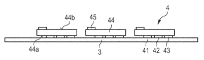
도 1a는 다수의 CMOS-칩(10)을 구비한 칩-복합체(1)를 개략적인 단면도로 보여준다. 각각의 CMOS-칩(10)의 상부면(10a)에는 3개의 접속 지점(2)이 배치되어 있다. 각각의 접속 지점(2)은 발광 다이오드의 반도체 몸체에 전류를 공급받기 위해서 제공되어 있다. 1A shows in schematic cross-sectional view a chip-composite 1 with a plurality of
도 1b의 개략적인 단면도에는 공통의 캐리어(3), 예컨대 박막 상에 배치되어 있는 3개의 발광 다이오드(4)가 도시되어 있다. 상기 발광 다이오드들(4)은, 도 1c에 도시된 바와 같이 캐리어(3)로부터 개별적으로 분리될 수 있다.In the schematic cross-sectional view of FIG. 1B there is shown a
각각의 발광 다이오드(4)는 방사선 투과성 캐리어(44)를 포함하고, 상기 방사선 투과성 캐리어의 상부면(44a)에는 각각 3개의 반도체 몸체(41, 42, 43)가 배치되어 있다. 상기 반도체 몸체들(41, 42, 43)은 공간적으로 서로 분리되어 있으며 상기 방사선 투과성 캐리어(44)를 통해서만 서로 연결되어 있다.Each
방사선 캐리어(44)로서는 투명한 플라스틱 박막이 사용된다. As the
또한, 각각의 발광 다이오드(4)는 상부면(44a)으로부터 떨어져서 마주한 캐리어(44)의 하부면(44b)에, 반도체 몸체들(41, 42, 43)이 예를 들어 n-측에서 콘택팅될 수 있는 접속 지점(45)을 포함한다. In addition, each
본 발명에서 반도체 몸체들(41, 42, 43)로서는, 작동 중에 다른 색의 전자기 방사선을 발생시키기 위해 각각 제공된 서로 상이한 반도체 몸체들이 사용된다. 예를 들어 반도체 몸체(41)는 작동 중에 적색 광을 발생하고, 반도체 몸체(42)는 작동 중에 녹색 광을 발생하며, 반도체 몸체(43)는 작동 중에 청색 광을 발생한다. As the
도 1c의 개략적인 도면에 따르면, 발광 다이오드들(4)은 간단한 방식으로 캐리어(3)로부터 분리될 수 있다. 발광 다이오드들(4)로서는, 칩-복합체(1)의 CMOS-칩(10) 상에 서로 분리되어 배치될 수 있는 분리 부품들이 사용된다. 이 경우 상기 발광 다이오드들(4)은 캐리어(44)의 상부면(44a)과 칩(10)의 상부면(10a)이 서로 마주 보고 놓이도록 CMOS-칩들(10) 상에 배치된다. 이 경우 각각의 발광 다이오드(4)의 반도체 몸체(41, 42, 43) 각각은 CMOS-칩(10)의 관련된 접속 지점(2)에 기계적으로 고정되고 상기 접속 지점에 전기적으로 콘택팅되어 있다(도 1e와 비교).According to the schematic drawing of FIG. 1C, the
마지막 방법 단계에서는 발광 다이오드들(4) 및 CMOS-칩들(10)로 이루어진 복합체가 분리될 수 있다. 이 경우에는 형성될 수 있는 가장 작은 유닛이 정확히 하나의 CMOS-칩(10) 및 하나의 할당된 발광 다이오드(4)를 포함한다. 다시 말하자면, CMOS-칩들(10)의 측면들(10c)은 분리에 의해 형성되고 분리 공정의 흔적들, 예를 들어 톱니 그루우브들을 갖는다.In the last method step, the composite consisting of the
그러나 조명 수단들(100)이 각각 다수의 CMOS-칩(10) 및 다수의 발광 다이오드(4)를 포함하는 것도 가능하다. 이러한 경우에 상기 조명 수단(100)은, 각각의 발광 다이오드(4)가 픽셀을 표현하는 풀-컬러 디스플레이로서 특히 우수하게 적합하며, 상기 픽셀은 각각 반도체 몸체들(41, 42, 43)로 형성되어 있는 3개의 하위 픽셀을 포함한다. However, it is also possible for the lighting means 100 to comprise a plurality of
예를 들어 도 1f에 도시된 조명 수단과 같은, 정확히 하나의 발광 다이오드(4) 및 정확히 하나의 CMOS-칩(10)을 갖는 조명 수단들(100)은 예컨대 광원으로서 광학 투사 장치들에 사용될 수 있다. Lighting means 100 with exactly one
CMOS-칩(10)을 통해서는 반도체 몸체들(41, 42, 43)이 사전 설정 가능한 방식에 의해 작동될 수 있다.Through the
도 2a 내지 도 2c와 관련해서는 본 발명에 기술된 방법의 대안적인 실시 예가 더 자세히 설명되어 있다. 상기 실시 예에서는 반도체 몸체들(41, 42, 43)이 동일한 형태로 형성되어 있다. 다시 말해, 각각 하나의 발광 다이오드(4)의 반도체 몸체들(41, 42, 43)은 작동 중에 동일한 스펙트럼 영역으로부터 전자기 방사선을 발생한다. 2A-2C, alternative embodiments of the method described herein are described in more detail. In the above embodiment, the
예를 들어, 반도체 몸체들(41, 42, 43)은 작동 중에 UV-방사선을 발생한다. 도 2a의 개략적인 단면도에 따르면, 발광 다이오드들(4)은 이미 칩-복합체(1) 상에 제공되어 있고, 각각의 반도체 몸체(41, 42, 43)는 할당된 CMOS-칩(10a)의 할당된 접속 지점(2)과 연결되어 있다. 이제 변환 소자들(51, 52, 53)은 각각 발광 다이오드들(4) 상으로 제공되며, 상기 변환 소자들은 이 변환 소자들이 반도체 몸체의 방사 방향으로 볼 때 할당된 상기 반도체 몸체(41, 42, 43) 다음에 배치되도록 각각의 캐리어의 하부면(44b)에 고정된다.For example, the
예를 들어 변환 소자들(51, 52, 53)은 발광 다이오드들 상에 제공되기 전에 공통의 캐리어(5) 상에 제공된다. 상기 변환 소자들은 예를 들어 반도체 재료, 예컨대 II/VI-반도체 재료에 의해 형성될 수 있다. 상기 변환 소자들은 캐리어(5)에 에피택셜 방식으로 증착될 수 있다. 하지만, 이 경우에는 복합체 내에, 즉 공통의 캐리어 (5) 상에, 또는 개별적으로 발광 다이오드(4) 상에 제공되는 세라믹 변환 소자들도 사용 가능하다. For example, the
캐리어(5)로부터 분리한 후 조명 수단이 만들어지며, 상기 조명 수단에서는 각각의 발광 다이오드(4)의 각각의 반도체 몸체(41, 42, 43) 다음에는 변환 소자(51, 52, 53)가 배치되어 있다. 작동 중에 상기 반도체 몸체들로부터 발생된 전자기 방사선은 예를 들어, 방사선 투과성 캐리어(44)를 통과하고 그곳에서 가급적 완전히 가시 광으로 파장 변환된다. 그럼으로써, 각각의 발광 다이오드는 예를 들어 적색, 녹색 및 청색 광의 방사에 적합하다.After separating from the carrier 5 an illumination means is made, in which the
도 2c에 도시된 바와 같이, 칩-복합체(1)는 조명 수단(100) 내에서 필요에 따라 양단될 수 있고, 분리시에는 재차 온전히 칩-복합체(1)에 의해서만 분리되며, 발광 다이오드(4)에 의해서는 분리되지 않는다. As shown in FIG. 2C, the chip-composite 1 can be cut off as necessary in the lighting means 100, again separated only by the chip-composite 1 again, and the light-emitting diode 4 ) Are not separated.
본 특허 출원서는 독일 특허 출원 102009033915.9호의 우선권을 주장하며, 상기 우선권 문서의 공개 내용은 인용의 방식으로 본 출원서에 수용된다. This patent application claims the priority of German Patent Application No. 102009033915.9, the disclosure of which priority document is incorporated herein by way of citation.
본 발명은 실시 예들을 참조한 상세한 설명에 한정되지 않는다. 오히려 본 발명은 각각의 새로운 특징 그리고 각각의 특징 조합을 포함하며, 상기 특징 또는 상기와 같은 조합 자체가 특허 청구 범위 또는 실시 예들에 명시적으로 기재되어 있지 않더라도 특히 각각의 특징 조합은 특허 청구범위에 포함된 것으로 간주된다. The invention is not limited to the detailed description with reference to the embodiments. Rather, the invention encompasses each new feature and each feature combination, in particular each feature combination being covered by the claims, even if such feature or such combination itself is not expressly described in the claims or the examples. It is considered to be included.
Claims (10)
다수의 발광 다이오드(4)를 준비하는 단계 ? 이때 각각의 발광 다이오드는 방사선 투과성 캐리어(44) 및 공간적으로 서로 분리된 2개 이상의 반도체 몸체(41, 42, 43)를 구비하고, 각각의 반도체 몸체(41, 42, 43)는 전자기 방사선을 발생시키기 위해 제공되어 있으며, 상기 반도체 몸체들(41, 42, 43)은 서로 분리하여 작동될 수 있고, 상기 반도체 몸체들(41, 42, 43)은 방사선 투과성 캐리어(44) 상에서 상기 방사선 투과성 캐리어(44)의 상부면(44a)에 배치되어 있음 ?;
CMOS-칩들(10)로 이루어진 칩-복합체(1)를 준비하는 단계 ? 이때 각각의 CMOS-칩(10)은 자체 상부면(10a)에 2개 이상의 접속 지점(2)을 가짐 ?;
상기 발광 다이오드들 중 하나 이상의 발광 다이오드(4)를 상기 CMOS-칩들 중 하나의 CMOS-칩(10)에 연결하는 단계 ? 이때 상기 발광 다이오드(4)는 상기 CMOS-칩(10)의 상부면(10a)에 있는 상기 방사선 투과성 캐리어(44)의 상부면(44a)에 배치되며, 발광 다이오드의 각각의 반도체 몸체(41, 42, 43)는 상기 CMOS-칩(10)의 접속 지점(2)에 연결됨 ?,
조명 수단을 제조하기 위한 방법.As a method for manufacturing the lighting means,
Preparing a plurality of light emitting diodes 4? In this case, each light emitting diode has a radiation transmitting carrier 44 and two or more semiconductor bodies 41, 42, 43 which are spatially separated from each other, and each semiconductor body 41, 42, 43 generates electromagnetic radiation. And the semiconductor bodies 41, 42, 43 can be operated separately from each other, and the semiconductor bodies 41, 42, 43 can be operated on a radioactive carrier 44. Disposed on the upper surface 44a of 44;
Preparing a chip-composite 1 consisting of CMOS chips 10? Wherein each CMOS chip 10 has at least two connection points 2 on its top surface 10a;
Connecting at least one light emitting diode 4 of the light emitting diodes to a CMOS chip 10 of one of the CMOS chips. In this case, the light emitting diodes 4 are disposed on the top surface 44a of the radiation transmitting carrier 44 in the top surface 10a of the CMOS chip 10, and each semiconductor body 41, 42 and 43 are connected to the connection point 2 of the CMOS chip 10?
Method for manufacturing the lighting means.
상기 접속 지점(2)은 방사선 투과성 캐리어(44)로부터 떨어져서 마주하는 상기 반도체 몸체(41, 42, 43)의 표면과 직접 접촉되는,
조명 수단을 제조하기 위한 방법.The method of claim 1,
The connection point 2 is in direct contact with the surface of the semiconductor body 41, 42, 43 facing away from the radioactive carrier 44,
Method for manufacturing the lighting means.
상기 반도체 몸체들(41, 42, 43)로부터 떨어져서 마주하는, 상기 하나 이상의 반도체 몸체(41, 42, 43)를 위한 상기 방사선 투과성 캐리어(44)의 하부면(44b)에서 변환 소자(51, 52, 53)는, 상기 반도체 몸체(41, 42, 43)의 작동 중에 상기 반도체 몸체로부터 방출된 전자기 방사선이 상기 변환 소자(51, 52, 53)를 통과하고 상기 변환 소자에 의해 적어도 부분적으로 파장 변환되도록 상기 방사선 투과성 캐리어(44) 상에 제공되는,
조명 수단을 제조하기 위한 방법.The method according to claim 1 or 2,
Conversion elements 51, 52 at the bottom surface 44b of the radiation transmissive carrier 44 for the one or more semiconductor bodies 41, 42, 43 facing away from the semiconductor bodies 41, 42, 43. , 53 indicates that electromagnetic radiation emitted from the semiconductor body during operation of the semiconductor bodies 41, 42, 43 passes through the conversion elements 51, 52, 53 and is at least partially wavelength converted by the conversion element. Provided on the radiolucent carrier 44 as
Method for manufacturing the lighting means.
복합체 내에 있는 다수의 변환 소자(51, 52, 53)는 동시에 다수의 발광 다이오드(4)와 연결되는,
조명 수단을 제조하기 위한 방법.The method of claim 3, wherein
The plurality of conversion elements 51, 52, 53 in the composite are simultaneously connected with the plurality of light emitting diodes 4,
Method for manufacturing the lighting means.
칩-복합체(1) 및 다수의 발광 다이오드(4)로 이루어진 복합체가 개별 조명 수단들로 분리되고, 상기 조명 수단들 중 각각의 조명 수단은 하나 이상의 발광 다이오드(4)를 포함하며, 상기 분리 과정 시에는 칩-복합체(1)만 양단되는,
조명 수단을 제조하기 위한 방법.The method according to any one of claims 1 to 4,
A composite consisting of a chip-composite 1 and a plurality of light emitting diodes 4 is separated into individual lighting means, each of the lighting means comprising one or more light emitting diodes 4, the separation process At the time, only the chip-composite 1
Method for manufacturing the lighting means.
이때 상기 CMOS-칩(10)은 자체 상부면에 2개 이상의 접속 지점(2)을 가지며,
이때 상기 발광 다이오드(4)는 방사선 투과성 캐리어(44) 및 공간적으로 서로 분리된 2개 이상의 반도체 몸체(41, 42, 43)를 구비하고, 각각의 반도체 몸체(41, 42, 43)는 전자기 방사선을 발생하기 위해 제공되어 있으며, 상기 반도체 몸체들(41, 42, 43)은 서로 분리하여 작동될 수 있고, 상기 반도체 몸체들(41, 42, 43)은 상기 방사선 투과성 캐리어(44) 상에서 방사선 투과성 캐리어의 상부면(44a)에 배치되어 있으며, 이때
상기 발광 다이오드(4) 및 CMOS-칩(10)의 상부면들(44a, 10a)은 서로 마주보며, 상기 하나 이상의 발광 다이오드(4)의 각각의 반도체 몸체(41, 42, 43)는 상기 CMOS-칩(10)의 접속 지점(2)과 연결되어 있는,
조명 수단.As a lighting means having a CMOS chip (10) and a light emitting diode (4),
In this case, the CMOS chip 10 has two or more connection points 2 on its upper surface,
In this case, the light emitting diode 4 has a radiation-transmissive carrier 44 and two or more semiconductor bodies 41, 42, 43 which are spatially separated from each other, and each semiconductor body 41, 42, 43 has an electromagnetic radiation. And the semiconductor bodies 41, 42, 43 can be operated separately from each other, and the semiconductor bodies 41, 42, 43 are transmissive on the radiation transmitting carrier 44. Disposed on the upper surface 44a of the carrier,
The light emitting diodes 4 and the upper surfaces 44a and 10a of the CMOS chip 10 face each other, and each semiconductor body 41, 42, 43 of the one or more light emitting diodes 4 is connected to the CMOS. Connected to the connection point 2 of the chip 10,
Lighting means.
상기 하나 이상의 발광 다이오드(4)는 반도체 몸체들(41, 42, 43)로부터 떨어져서 마주한 상기 발광 다이오드의 방사선 투과성 캐리어(44)의 측에 접속 지점(45)을 구비하며, 상기 접속 지점은 상기 발광 다이오드(4)의 모든 반도체 몸체(41, 42, 43)의 공통의 전기 콘택팅을 위해 제공되어 있는,
조명 수단.The method according to claim 6,
The at least one light emitting diode 4 has a connection point 45 on the side of the radioactive carrier 44 of the light emitting diode facing away from the semiconductor bodies 41, 42, 43, the connection point being the light emission. Provided for the common electrical contacting of all the semiconductor bodies 41, 42, 43 of the diode 4,
Lighting means.
상기 하나 이상의 발광 다이오드(4)의 모든 반도체 몸체(41, 42, 43)가 동일한 스펙트럼 영역에서 전자기 방사선을 발생시키고, 상기 반도체 몸체들(41, 42, 43) 중 하나 이상의 반도체 몸체 다음에는 변환 소자(51, 52, 53)가 배치되어 있으며, 이때 상기 변환 소자(51, 52, 53)는, 상기 반도체 몸체(41, 42, 43)의 작동 중에 상기 반도체 몸체로부터 방출된 전자기 방사선이 상기 변환 소자(51, 52, 53)를 통과하고 상기 변환 소자로부터 적어도 부분적으로 파장 변환되도록 상기 반도체 몸체(41, 42, 43)로부터 떨어져서 마주하는 상기 방사선 투과성 캐리어(44)의 하부면(44b)에 배치되어 있는,
조명 수단을 제조하기 위한 방법 또는 조명 수단.A method or lighting means for producing the lighting means according to any one of claims 1 to 7,
All semiconductor bodies 41, 42, 43 of the one or more light emitting diodes 4 generate electromagnetic radiation in the same spectral region, followed by one or more semiconductor bodies of the semiconductor bodies 41, 42, 43. (51, 52, 53) is disposed, wherein the conversion element (51, 52, 53), the electromagnetic radiation emitted from the semiconductor body during the operation of the semiconductor body (41, 42, 43) is the conversion element Disposed on the lower surface 44b of the radioactive carrier 44 facing away from the semiconductor body 41, 42, 43 to pass through (51, 52, 53) and at least partially wavelength convert from the conversion element. there is,
Method or lighting means for manufacturing the lighting means.
상기 하나 이상의 발광 다이오드(4)의 2개 이상의 반도체 몸체(41, 42, 43)가 작동 중에 서로 상이한 스펙트럼 영역들로부터 전자기 방사선을 발생시키는,
조명 수단을 제조하기 위한 방법 또는 조명 수단.The method according to any one of claims 1 to 8,
Two or more semiconductor bodies 41, 42, 43 of the at least one light emitting diode 4 generate electromagnetic radiation from different spectral regions during operation,
Method or lighting means for manufacturing the lighting means.
상기 하나 이상의 발광 다이오드의 방사선 투과성 캐리어(44)가 플라스틱 박막을 포함하고, 상기 플라스틱 박막 내부로 그리고/또는 상기 플라스틱 박막 상으로 상기 반도체 몸체들(41, 42, 43)의 콘택팅을 위한 전기 라인들이 배치되어 있는,
조명 수단을 제조하기 위한 방법 또는 조명 수단.The method according to any one of claims 1 to 9,
The radiation-transmitting carrier 44 of the at least one light emitting diode comprises a plastic thin film and an electrical line for contacting the semiconductor bodies 41, 42, 43 into and / or onto the plastic thin film. Is placed,
Method or lighting means for manufacturing the lighting means.
Applications Claiming Priority (2)
| Application Number | Priority Date | Filing Date | Title |
|---|---|---|---|
| DE102009033915.9A DE102009033915B4 (en) | 2009-07-20 | 2009-07-20 | Method of manufacturing a lighting device and lighting device |
| DE102009033915.9 | 2009-07-20 |
Publications (1)
| Publication Number | Publication Date |
|---|---|
| KR20120038511A true KR20120038511A (en) | 2012-04-23 |
Family
ID=43016842
Family Applications (1)
| Application Number | Title | Priority Date | Filing Date |
|---|---|---|---|
| KR1020127004430A KR20120038511A (en) | 2009-07-20 | 2010-07-16 | Method for manufacturing a light source and light source |
Country Status (6)
| Country | Link |
|---|---|
| EP (1) | EP2457254B1 (en) |
| JP (1) | JP5813636B2 (en) |
| KR (1) | KR20120038511A (en) |
| CN (1) | CN102473704A (en) |
| DE (1) | DE102009033915B4 (en) |
| WO (1) | WO2011009821A1 (en) |
Families Citing this family (3)
| Publication number | Priority date | Publication date | Assignee | Title |
|---|---|---|---|---|
| DE102012202928A1 (en) * | 2012-02-27 | 2013-08-29 | Osram Gmbh | LIGHT SOURCE WITH LED CHIP AND FLUORESCENT LAYER |
| DE102013205179A1 (en) | 2013-03-25 | 2014-09-25 | Osram Gmbh | A method of manufacturing an electromagnetic radiation emitting assembly and electromagnetic radiation emitting assembly |
| KR20200062762A (en) | 2018-11-27 | 2020-06-04 | 삼성전자주식회사 | Micro light source array, display device having the same and method of manufacturing display device |
Family Cites Families (12)
| Publication number | Priority date | Publication date | Assignee | Title |
|---|---|---|---|---|
| US5940683A (en) * | 1996-01-18 | 1999-08-17 | Motorola, Inc. | LED display packaging with substrate removal and method of fabrication |
| JP3473396B2 (en) * | 1998-04-23 | 2003-12-02 | 松下電器産業株式会社 | Optical information processing device |
| EP0977063A1 (en) * | 1998-07-28 | 2000-02-02 | Interuniversitair Micro-Elektronica Centrum Vzw | A socket and a system for optoelectronic interconnection and a method of fabricating such socket and system |
| JP3652945B2 (en) * | 1999-12-28 | 2005-05-25 | 松下電器産業株式会社 | Optical information processing equipment |
| JP4182661B2 (en) * | 2001-10-31 | 2008-11-19 | ソニー株式会社 | Image display device and manufacturing method thereof |
| JP2005093649A (en) * | 2003-09-17 | 2005-04-07 | Oki Data Corp | Semiconductor composite device, led print head, and image forming apparatus using same |
| US7294961B2 (en) * | 2004-03-29 | 2007-11-13 | Articulated Technologies, Llc | Photo-radiation source provided with emissive particles dispersed in a charge-transport matrix |
| CN1622730A (en) * | 2004-12-16 | 2005-06-01 | 新磊微制造股份有限公司 | Luminous module |
| TWI420691B (en) * | 2006-11-20 | 2013-12-21 | 尼康股份有限公司 | Led device and the fabricating method thereof |
| DE102007010244A1 (en) * | 2007-02-02 | 2008-08-07 | Osram Opto Semiconductors Gmbh | Arrangement and method for generating mixed light |
| JP2008262993A (en) * | 2007-04-10 | 2008-10-30 | Nikon Corp | Display device |
| EP1988577B1 (en) * | 2007-04-30 | 2017-04-05 | Tridonic Jennersdorf GmbH | Light emitting diode module with silicon platform |
-
2009
- 2009-07-20 DE DE102009033915.9A patent/DE102009033915B4/en not_active Expired - Fee Related
-
2010
- 2010-07-16 WO PCT/EP2010/060345 patent/WO2011009821A1/en active Application Filing
- 2010-07-16 KR KR1020127004430A patent/KR20120038511A/en not_active Application Discontinuation
- 2010-07-16 EP EP10734486.3A patent/EP2457254B1/en active Active
- 2010-07-16 CN CN2010800331752A patent/CN102473704A/en active Pending
- 2010-07-16 JP JP2012521009A patent/JP5813636B2/en not_active Expired - Fee Related
Also Published As
| Publication number | Publication date |
|---|---|
| WO2011009821A1 (en) | 2011-01-27 |
| DE102009033915A1 (en) | 2011-01-27 |
| CN102473704A (en) | 2012-05-23 |
| EP2457254B1 (en) | 2020-03-18 |
| EP2457254A1 (en) | 2012-05-30 |
| JP5813636B2 (en) | 2015-11-17 |
| DE102009033915B4 (en) | 2022-05-25 |
| JP2012533895A (en) | 2012-12-27 |
Similar Documents
| Publication | Publication Date | Title |
|---|---|---|
| CN109937480B (en) | Multi-pixel LED component and method for operating a multi-pixel LED component | |
| TWI384637B (en) | Semiconductor light emitting device, light emitting module, lighting apparatus, display element and manufacturing method of semiconductor light emitting device | |
| US20200051967A1 (en) | Led display modules and methods for making the same | |
| JP3934590B2 (en) | White light emitting device and manufacturing method thereof | |
| US9543221B2 (en) | Method of manufacturing light-emitting apparatus, light-emitting module inspecting apparatus, and method of determining whether light-emitting module meets quality requirement | |
| US11069663B2 (en) | Method of producing an optoelectronic semiconductor component, and optoelectronic semiconductor component | |
| US20100301355A1 (en) | Optoelectronic Component and Production Method for an Optoelectronic Component | |
| US9142721B2 (en) | Semiconductor light emitting device and manufacturing method of the same | |
| JP2010041057A (en) | Semiconductor device and method of manufacturing the same | |
| WO2015117273A1 (en) | Smart pixel surface mount device package | |
| US11164850B2 (en) | Arrangement comprising a plurality of lighting modules and method for producing an arrangement comprising a plurality of lighting modules | |
| US9257623B2 (en) | Light-emitting diode package | |
| US20150260351A1 (en) | Light-emitting device, illumination light source, and illumination device | |
| JP2016167518A (en) | Light emission device and luminaire | |
| JP2005109113A (en) | Semiconductor light-emitting device, method for manufacturing the same light-emitting module, and lighting system | |
| US20150292682A1 (en) | Lighting apparatus | |
| KR20120038511A (en) | Method for manufacturing a light source and light source | |
| KR20150000676A (en) | Method for manufacturing semiconductor light emitting device package | |
| KR20120085085A (en) | Cob type light emitting module and method of the light emitting module | |
| KR20170047641A (en) | 3d full color display using micro leds | |
| JP6941923B2 (en) | LED module manufacturing method and LED module | |
| US8273588B2 (en) | Method for producing a luminous device and luminous device | |
| KR101460380B1 (en) | Arrangement for generating mixed light,and method for the production of such an arrangement | |
| US8562142B2 (en) | Projector for micro projection surfaces and use of a multicolour LED in a projector | |
| WO2014032702A1 (en) | Light-emitting device and method for manufacturing a light- emitting device |
Legal Events
| Date | Code | Title | Description |
|---|---|---|---|
| WITN | Application deemed withdrawn, e.g. because no request for examination was filed or no examination fee was paid |