KR20200062762A - Micro light source array, display device having the same and method of manufacturing display device - Google Patents
Micro light source array, display device having the same and method of manufacturing display device Download PDFInfo
- Publication number
- KR20200062762A KR20200062762A KR1020180148546A KR20180148546A KR20200062762A KR 20200062762 A KR20200062762 A KR 20200062762A KR 1020180148546 A KR1020180148546 A KR 1020180148546A KR 20180148546 A KR20180148546 A KR 20180148546A KR 20200062762 A KR20200062762 A KR 20200062762A
- Authority
- KR
- South Korea
- Prior art keywords
- sub
- silicon
- light source
- mounts
- mount
- Prior art date
Links
- 238000004519 manufacturing process Methods 0.000 title claims abstract description 28
- 229910052710 silicon Inorganic materials 0.000 claims abstract description 103
- 239000010703 silicon Substances 0.000 claims abstract description 103
- 239000000758 substrate Substances 0.000 claims abstract description 49
- XUIMIQQOPSSXEZ-UHFFFAOYSA-N Silicon Chemical compound [Si] XUIMIQQOPSSXEZ-UHFFFAOYSA-N 0.000 claims description 101
- 238000000034 method Methods 0.000 claims description 34
- 238000006243 chemical reaction Methods 0.000 claims description 6
- 238000005498 polishing Methods 0.000 claims description 2
- 239000010410 layer Substances 0.000 description 17
- 239000004065 semiconductor Substances 0.000 description 11
- 238000003491 array Methods 0.000 description 10
- 239000011159 matrix material Substances 0.000 description 7
- 239000000463 material Substances 0.000 description 6
- 229910044991 metal oxide Inorganic materials 0.000 description 6
- 150000004706 metal oxides Chemical class 0.000 description 6
- 239000002096 quantum dot Substances 0.000 description 6
- 239000003990 capacitor Substances 0.000 description 3
- 230000000295 complement effect Effects 0.000 description 3
- 229920001940 conductive polymer Polymers 0.000 description 2
- 239000004020 conductor Substances 0.000 description 2
- 230000007423 decrease Effects 0.000 description 2
- 230000014509 gene expression Effects 0.000 description 2
- 229910052751 metal Inorganic materials 0.000 description 2
- 239000002184 metal Substances 0.000 description 2
- 239000000203 mixture Substances 0.000 description 2
- 239000002245 particle Substances 0.000 description 2
- 229910004613 CdTe Inorganic materials 0.000 description 1
- 229910001218 Gallium arsenide Inorganic materials 0.000 description 1
- 229910000673 Indium arsenide Inorganic materials 0.000 description 1
- ZOKXTWBITQBERF-UHFFFAOYSA-N Molybdenum Chemical compound [Mo] ZOKXTWBITQBERF-UHFFFAOYSA-N 0.000 description 1
- BQCADISMDOOEFD-UHFFFAOYSA-N Silver Chemical compound [Ag] BQCADISMDOOEFD-UHFFFAOYSA-N 0.000 description 1
- RTAQQCXQSZGOHL-UHFFFAOYSA-N Titanium Chemical compound [Ti] RTAQQCXQSZGOHL-UHFFFAOYSA-N 0.000 description 1
- 229910007709 ZnTe Inorganic materials 0.000 description 1
- 239000012790 adhesive layer Substances 0.000 description 1
- 229910045601 alloy Inorganic materials 0.000 description 1
- 239000000956 alloy Substances 0.000 description 1
- 229910052782 aluminium Inorganic materials 0.000 description 1
- XAGFODPZIPBFFR-UHFFFAOYSA-N aluminium Chemical compound [Al] XAGFODPZIPBFFR-UHFFFAOYSA-N 0.000 description 1
- UHYPYGJEEGLRJD-UHFFFAOYSA-N cadmium(2+);selenium(2-) Chemical compound [Se-2].[Cd+2] UHYPYGJEEGLRJD-UHFFFAOYSA-N 0.000 description 1
- 239000002238 carbon nanotube film Substances 0.000 description 1
- 239000003086 colorant Substances 0.000 description 1
- 150000001875 compounds Chemical class 0.000 description 1
- 239000013078 crystal Substances 0.000 description 1
- 238000000708 deep reactive-ion etching Methods 0.000 description 1
- -1 for example Substances 0.000 description 1
- 229910052733 gallium Inorganic materials 0.000 description 1
- PCHJSUWPFVWCPO-UHFFFAOYSA-N gold Chemical compound [Au] PCHJSUWPFVWCPO-UHFFFAOYSA-N 0.000 description 1
- 239000010931 gold Substances 0.000 description 1
- 229910052737 gold Inorganic materials 0.000 description 1
- RPQDHPTXJYYUPQ-UHFFFAOYSA-N indium arsenide Chemical compound [In]#[As] RPQDHPTXJYYUPQ-UHFFFAOYSA-N 0.000 description 1
- 238000007641 inkjet printing Methods 0.000 description 1
- 230000001678 irradiating effect Effects 0.000 description 1
- 238000012986 modification Methods 0.000 description 1
- 230000004048 modification Effects 0.000 description 1
- 229910052750 molybdenum Inorganic materials 0.000 description 1
- 239000011733 molybdenum Substances 0.000 description 1
- 230000000149 penetrating effect Effects 0.000 description 1
- 238000001020 plasma etching Methods 0.000 description 1
- 229920001296 polysiloxane Polymers 0.000 description 1
- 229910052594 sapphire Inorganic materials 0.000 description 1
- 239000010980 sapphire Substances 0.000 description 1
- 238000007650 screen-printing Methods 0.000 description 1
- SBIBMFFZSBJNJF-UHFFFAOYSA-N selenium;zinc Chemical compound [Se]=[Zn] SBIBMFFZSBJNJF-UHFFFAOYSA-N 0.000 description 1
- 238000000926 separation method Methods 0.000 description 1
- 229910052709 silver Inorganic materials 0.000 description 1
- 239000004332 silver Substances 0.000 description 1
- 230000002194 synthesizing effect Effects 0.000 description 1
- 229910052719 titanium Inorganic materials 0.000 description 1
- 239000010936 titanium Substances 0.000 description 1
- WFKWXMTUELFFGS-UHFFFAOYSA-N tungsten Chemical compound [W] WFKWXMTUELFFGS-UHFFFAOYSA-N 0.000 description 1
- 229910052721 tungsten Inorganic materials 0.000 description 1
- 239000010937 tungsten Substances 0.000 description 1
- 238000000378 two-dimensional separation method Methods 0.000 description 1
Images


Classifications
-
- H—ELECTRICITY
- H01—ELECTRIC ELEMENTS
- H01L—SEMICONDUCTOR DEVICES NOT COVERED BY CLASS H10
- H01L27/00—Devices consisting of a plurality of semiconductor or other solid-state components formed in or on a common substrate
- H01L27/02—Devices consisting of a plurality of semiconductor or other solid-state components formed in or on a common substrate including semiconductor components specially adapted for rectifying, oscillating, amplifying or switching and having at least one potential-jump barrier or surface barrier; including integrated passive circuit elements with at least one potential-jump barrier or surface barrier
- H01L27/12—Devices consisting of a plurality of semiconductor or other solid-state components formed in or on a common substrate including semiconductor components specially adapted for rectifying, oscillating, amplifying or switching and having at least one potential-jump barrier or surface barrier; including integrated passive circuit elements with at least one potential-jump barrier or surface barrier the substrate being other than a semiconductor body, e.g. an insulating body
- H01L27/1214—Devices consisting of a plurality of semiconductor or other solid-state components formed in or on a common substrate including semiconductor components specially adapted for rectifying, oscillating, amplifying or switching and having at least one potential-jump barrier or surface barrier; including integrated passive circuit elements with at least one potential-jump barrier or surface barrier the substrate being other than a semiconductor body, e.g. an insulating body comprising a plurality of TFTs formed on a non-semiconducting substrate, e.g. driving circuits for AMLCDs
- H01L27/1259—Multistep manufacturing methods
- H01L27/1262—Multistep manufacturing methods with a particular formation, treatment or coating of the substrate
- H01L27/1266—Multistep manufacturing methods with a particular formation, treatment or coating of the substrate the substrate on which the devices are formed not being the final device substrate, e.g. using a temporary substrate
-
- H—ELECTRICITY
- H01—ELECTRIC ELEMENTS
- H01L—SEMICONDUCTOR DEVICES NOT COVERED BY CLASS H10
- H01L25/00—Assemblies consisting of a plurality of individual semiconductor or other solid state devices ; Multistep manufacturing processes thereof
- H01L25/03—Assemblies consisting of a plurality of individual semiconductor or other solid state devices ; Multistep manufacturing processes thereof all the devices being of a type provided for in the same subgroup of groups H01L27/00 - H01L33/00, or in a single subclass of H10K, H10N, e.g. assemblies of rectifier diodes
- H01L25/04—Assemblies consisting of a plurality of individual semiconductor or other solid state devices ; Multistep manufacturing processes thereof all the devices being of a type provided for in the same subgroup of groups H01L27/00 - H01L33/00, or in a single subclass of H10K, H10N, e.g. assemblies of rectifier diodes the devices not having separate containers
- H01L25/075—Assemblies consisting of a plurality of individual semiconductor or other solid state devices ; Multistep manufacturing processes thereof all the devices being of a type provided for in the same subgroup of groups H01L27/00 - H01L33/00, or in a single subclass of H10K, H10N, e.g. assemblies of rectifier diodes the devices not having separate containers the devices being of a type provided for in group H01L33/00
- H01L25/0753—Assemblies consisting of a plurality of individual semiconductor or other solid state devices ; Multistep manufacturing processes thereof all the devices being of a type provided for in the same subgroup of groups H01L27/00 - H01L33/00, or in a single subclass of H10K, H10N, e.g. assemblies of rectifier diodes the devices not having separate containers the devices being of a type provided for in group H01L33/00 the devices being arranged next to each other
-
- H—ELECTRICITY
- H01—ELECTRIC ELEMENTS
- H01L—SEMICONDUCTOR DEVICES NOT COVERED BY CLASS H10
- H01L25/00—Assemblies consisting of a plurality of individual semiconductor or other solid state devices ; Multistep manufacturing processes thereof
- H01L25/16—Assemblies consisting of a plurality of individual semiconductor or other solid state devices ; Multistep manufacturing processes thereof the devices being of types provided for in two or more different main groups of groups H01L27/00 - H01L33/00, or in a single subclass of H10K, H10N, e.g. forming hybrid circuits
- H01L25/167—Assemblies consisting of a plurality of individual semiconductor or other solid state devices ; Multistep manufacturing processes thereof the devices being of types provided for in two or more different main groups of groups H01L27/00 - H01L33/00, or in a single subclass of H10K, H10N, e.g. forming hybrid circuits comprising optoelectronic devices, e.g. LED, photodiodes
-
- H—ELECTRICITY
- H01—ELECTRIC ELEMENTS
- H01L—SEMICONDUCTOR DEVICES NOT COVERED BY CLASS H10
- H01L27/00—Devices consisting of a plurality of semiconductor or other solid-state components formed in or on a common substrate
- H01L27/02—Devices consisting of a plurality of semiconductor or other solid-state components formed in or on a common substrate including semiconductor components specially adapted for rectifying, oscillating, amplifying or switching and having at least one potential-jump barrier or surface barrier; including integrated passive circuit elements with at least one potential-jump barrier or surface barrier
- H01L27/04—Devices consisting of a plurality of semiconductor or other solid-state components formed in or on a common substrate including semiconductor components specially adapted for rectifying, oscillating, amplifying or switching and having at least one potential-jump barrier or surface barrier; including integrated passive circuit elements with at least one potential-jump barrier or surface barrier the substrate being a semiconductor body
- H01L27/08—Devices consisting of a plurality of semiconductor or other solid-state components formed in or on a common substrate including semiconductor components specially adapted for rectifying, oscillating, amplifying or switching and having at least one potential-jump barrier or surface barrier; including integrated passive circuit elements with at least one potential-jump barrier or surface barrier the substrate being a semiconductor body including only semiconductor components of a single kind
- H01L27/085—Devices consisting of a plurality of semiconductor or other solid-state components formed in or on a common substrate including semiconductor components specially adapted for rectifying, oscillating, amplifying or switching and having at least one potential-jump barrier or surface barrier; including integrated passive circuit elements with at least one potential-jump barrier or surface barrier the substrate being a semiconductor body including only semiconductor components of a single kind including field-effect components only
- H01L27/088—Devices consisting of a plurality of semiconductor or other solid-state components formed in or on a common substrate including semiconductor components specially adapted for rectifying, oscillating, amplifying or switching and having at least one potential-jump barrier or surface barrier; including integrated passive circuit elements with at least one potential-jump barrier or surface barrier the substrate being a semiconductor body including only semiconductor components of a single kind including field-effect components only the components being field-effect transistors with insulated gate
- H01L27/092—Devices consisting of a plurality of semiconductor or other solid-state components formed in or on a common substrate including semiconductor components specially adapted for rectifying, oscillating, amplifying or switching and having at least one potential-jump barrier or surface barrier; including integrated passive circuit elements with at least one potential-jump barrier or surface barrier the substrate being a semiconductor body including only semiconductor components of a single kind including field-effect components only the components being field-effect transistors with insulated gate complementary MIS field-effect transistors
-
- H—ELECTRICITY
- H01—ELECTRIC ELEMENTS
- H01L—SEMICONDUCTOR DEVICES NOT COVERED BY CLASS H10
- H01L27/00—Devices consisting of a plurality of semiconductor or other solid-state components formed in or on a common substrate
- H01L27/02—Devices consisting of a plurality of semiconductor or other solid-state components formed in or on a common substrate including semiconductor components specially adapted for rectifying, oscillating, amplifying or switching and having at least one potential-jump barrier or surface barrier; including integrated passive circuit elements with at least one potential-jump barrier or surface barrier
- H01L27/12—Devices consisting of a plurality of semiconductor or other solid-state components formed in or on a common substrate including semiconductor components specially adapted for rectifying, oscillating, amplifying or switching and having at least one potential-jump barrier or surface barrier; including integrated passive circuit elements with at least one potential-jump barrier or surface barrier the substrate being other than a semiconductor body, e.g. an insulating body
- H01L27/1214—Devices consisting of a plurality of semiconductor or other solid-state components formed in or on a common substrate including semiconductor components specially adapted for rectifying, oscillating, amplifying or switching and having at least one potential-jump barrier or surface barrier; including integrated passive circuit elements with at least one potential-jump barrier or surface barrier the substrate being other than a semiconductor body, e.g. an insulating body comprising a plurality of TFTs formed on a non-semiconducting substrate, e.g. driving circuits for AMLCDs
- H01L27/1218—Devices consisting of a plurality of semiconductor or other solid-state components formed in or on a common substrate including semiconductor components specially adapted for rectifying, oscillating, amplifying or switching and having at least one potential-jump barrier or surface barrier; including integrated passive circuit elements with at least one potential-jump barrier or surface barrier the substrate being other than a semiconductor body, e.g. an insulating body comprising a plurality of TFTs formed on a non-semiconducting substrate, e.g. driving circuits for AMLCDs with a particular composition or structure of the substrate
-
- H—ELECTRICITY
- H01—ELECTRIC ELEMENTS
- H01L—SEMICONDUCTOR DEVICES NOT COVERED BY CLASS H10
- H01L33/00—Semiconductor devices with at least one potential-jump barrier or surface barrier specially adapted for light emission; Processes or apparatus specially adapted for the manufacture or treatment thereof or of parts thereof; Details thereof
- H01L33/005—Processes
-
- H—ELECTRICITY
- H01—ELECTRIC ELEMENTS
- H01L—SEMICONDUCTOR DEVICES NOT COVERED BY CLASS H10
- H01L33/00—Semiconductor devices with at least one potential-jump barrier or surface barrier specially adapted for light emission; Processes or apparatus specially adapted for the manufacture or treatment thereof or of parts thereof; Details thereof
- H01L33/48—Semiconductor devices with at least one potential-jump barrier or surface barrier specially adapted for light emission; Processes or apparatus specially adapted for the manufacture or treatment thereof or of parts thereof; Details thereof characterised by the semiconductor body packages
- H01L33/483—Containers
- H01L33/486—Containers adapted for surface mounting
-
- H—ELECTRICITY
- H01—ELECTRIC ELEMENTS
- H01L—SEMICONDUCTOR DEVICES NOT COVERED BY CLASS H10
- H01L33/00—Semiconductor devices with at least one potential-jump barrier or surface barrier specially adapted for light emission; Processes or apparatus specially adapted for the manufacture or treatment thereof or of parts thereof; Details thereof
- H01L33/48—Semiconductor devices with at least one potential-jump barrier or surface barrier specially adapted for light emission; Processes or apparatus specially adapted for the manufacture or treatment thereof or of parts thereof; Details thereof characterised by the semiconductor body packages
- H01L33/50—Wavelength conversion elements
-
- H—ELECTRICITY
- H01—ELECTRIC ELEMENTS
- H01L—SEMICONDUCTOR DEVICES NOT COVERED BY CLASS H10
- H01L33/00—Semiconductor devices with at least one potential-jump barrier or surface barrier specially adapted for light emission; Processes or apparatus specially adapted for the manufacture or treatment thereof or of parts thereof; Details thereof
- H01L33/48—Semiconductor devices with at least one potential-jump barrier or surface barrier specially adapted for light emission; Processes or apparatus specially adapted for the manufacture or treatment thereof or of parts thereof; Details thereof characterised by the semiconductor body packages
- H01L33/62—Arrangements for conducting electric current to or from the semiconductor body, e.g. lead-frames, wire-bonds or solder balls
-
- H—ELECTRICITY
- H01—ELECTRIC ELEMENTS
- H01L—SEMICONDUCTOR DEVICES NOT COVERED BY CLASS H10
- H01L2933/00—Details relating to devices covered by the group H01L33/00 but not provided for in its subgroups
- H01L2933/0008—Processes
- H01L2933/0033—Processes relating to semiconductor body packages
Abstract
Description
예시적인 실시예는 마이크로 광원 어레이, 이를 포함한 디스플레이 장치 및 디스플레이 장치의 제조 방법에 관한 것이다. An exemplary embodiment relates to a micro light source array, a display device including the same, and a method of manufacturing the display device.
발광 다이오드(Light emitting diode; LED)는 저전력 사용과 친환경적이라는 장점이 있다. 이러한 장점 때문에 산업적인 수요가 증대되고 있다. LED는 조명 장치나 LCD 백라이트용으로 뿐만 아니라 LED 디스플레이 장치에도 적용되고 있다. 즉, 마이크로 단위의 LED 칩을 사용하는 디스플레이 장치가 개발되고 있다. 마이크로 LED 디스플레이 장치를 제작하는데 있어서, 마이크로 LED를 기판에 전사하는 것이 필요하다. 마이크로 LED를 전사하는 방법으로 픽 앤 플레이스(pick and place) 방법이 많이 사용되고 있다. 하지만, 이러한 방법은 마이크로 LED의 크기가 작아지고 디스플레이의 사이즈가 커짐에 따라 생산성이 저하된다. Light emitting diodes (LEDs) have the advantage of using low power and being environmentally friendly. Due to these advantages, industrial demand is increasing. LEDs are applied not only for lighting devices or LCD backlights, but also for LED display devices. That is, a display device using a micro unit LED chip has been developed. In manufacturing a micro LED display device, it is necessary to transfer the micro LED to the substrate. As a method of transferring the micro LED, a pick and place method is widely used. However, this method decreases productivity as the size of the micro LED becomes smaller and the size of the display increases.
다양한 실시예는 실리콘 서브 마운트에 정렬된 마이크로 광원 어레이를 제공한다.Various embodiments provide an array of micro light sources aligned to a silicon sub-mount.
다양한 실시예는 실리콘 서브 마운트에 정렬된 마이크로 광원 어레이를 포함하는 디스플레이 장치를 제공한다.Various embodiments provide a display device comprising an array of micro light sources aligned to a silicon sub-mount.
다양한 실시예는 디스플레이 장치의 제조 방법을 제공한다. Various embodiments provide a method of manufacturing a display device.
일 실시예에 따르면, 각각 독립적으로 구동되는 복수 개의 서브 픽셀을 포함하는 디스플레이 장치의 마이크로 광원 어레이에 있어서, 기판에 상기 서브 픽셀에 대응하여 구비되고, 트렌치에 의해 서로 이격되어 배열된 실리콘 서브 마운트; 상기 실리콘 서브 마운트에 결합된 발광 소자 칩; 및 상기 실리콘 서브 마운트에 구비된 구동 회로;를 포함한다.According to one embodiment, each of the micro light source array of the display device including a plurality of sub-pixels that are independently driven, comprising: a silicon sub-mount provided on the substrate corresponding to the sub-pixels and spaced apart from each other by a trench; A light emitting device chip coupled to the silicon sub-mount; And a driving circuit provided in the silicon sub-mount.
상기 구동 회로가 CMOS 또는 NMOS를 포함할 수 있다.The driving circuit may include CMOS or NMOS.
상기 실리콘 서브 마운트와 전기적으로 연결되는 배선을 더 포함할 수 있다. 상기 발광 소자 칩이 상기 실리콘 서브 마운트에 플립칩 본딩될 수 있다.A wire electrically connected to the silicon sub-mount may be further included. The light emitting device chip may be flip-chip bonded to the silicon sub-mount.
상기 이웃하는 실리콘 서브 마운트들이 가로 방향과 세로 방향에 대해 각각 상기 서브 픽셀의 피치 간격으로 이격되어 배치될 수 있다. The neighboring silicon sub-mounts may be disposed spaced apart at a pitch interval of the sub-pixels, respectively, in the horizontal direction and the vertical direction.
상기 발광 소자 칩은 마이크로 LED를 포함할 수 있다.The light emitting device chip may include a micro LED.
상기 발광 소자 칩은 청색 광을 발광할 수 있다.The light emitting device chip may emit blue light.
예시적인 실시예에 따른 디스플레이 장치는, 각각 독립적으로 구동되는 복수 개의 서브 픽셀을 포함하는 디스플레이 장치에 있어서, 기판; 상기 기판에 상기 서브 픽셀에 대응하여 구비되고, 트렌치에 의해 서로 이격되어 배열된 실리콘 서브 마운트; 상기 실리콘 서브 마운트에 결합된 발광 소자 칩; 상기 실리콘 서브 마운트에 구비된 구동 회로; 및 상기 발광 소자 칩 상에 구비되어 상기 발광 소자 칩으로부터 출사된 광의 칼라를 변환하는 칼라 변환 소자;를 포함한다. 예시적인 실시예에 따른 디스플레이 제조 방법은, A display device according to an exemplary embodiment includes: a display device including a plurality of sub-pixels each independently driven, comprising: a substrate; A silicon sub-mount provided on the substrate corresponding to the sub-pixel and arranged spaced apart from each other by a trench; A light emitting device chip coupled to the silicon sub-mount; A driving circuit provided in the silicon sub-mount; And a color conversion element provided on the light emitting element chip to convert the color of light emitted from the light emitting element chip. The display manufacturing method according to the exemplary embodiment,
실리콘 기판에 구동 회로를 형성하는 단계; 상기 실리콘 기판에 트렌치를 형성하는 단계; 상기 실리콘 기판에 발광 소자 어레이를 본딩하는 단계; 및 상기 실리콘 기판을 후면에서 상기 트렌치가 관통되도록 연마하여 서로 이격된 실리콘 서브 마운트를 형성하는 단계;를 포함한다.Forming a driving circuit on the silicon substrate; Forming a trench in the silicon substrate; Bonding a light emitting device array to the silicon substrate; And polishing the silicon substrate so that the trench is penetrated from the rear surface to form silicon sub-mounts spaced apart from each other.
상기 디스플레이 제조 방법은, 상기 서로 이격된 실리콘 서브 마운트를 타켓 기판에 전사하는 단계를 더 포함할 수 있다. 상기 디스플레이 제조 방법은, 상기 서로 이격된 실리콘 서브 마운트 사이의 가로 방향과 세로 방향 중 어느 한 방향으로 이동 소자를 삽입하고, 실리콘 서브 마운트 사이를 벌려 정렬하는 단계를 포함할 수 있다.The display manufacturing method may further include transferring the silicon sub-mounts spaced apart from each other to a target substrate. The display manufacturing method may include inserting moving elements in either a horizontal direction or a vertical direction between the silicon sub-mounts spaced apart from each other, and aligning the silicon sub-mounts.
상기 디스플레이 제조 방법은, 상기 실리콘 서브 마운트의 세로 방향과 가로 방향 중 다른 한 방향으로 이동 소자를 삽입하고, 실리콘 서브 마운트 사이를 벌려 정렬하는 단계를 포함할 수 있다. The display manufacturing method may include inserting a moving element in a different one of a vertical direction and a horizontal direction of the silicon sub-mount and aligning the silicon sub-mounts.
상기 디스플레이 제조 방법은, 상기 서로 이격된 실리콘 서브 마운트 사이의 제1 방향으로 이동 소자를 삽입하여 분리하는 단계를 포함할 수 있다.The display manufacturing method may include a step of inserting and separating a moving element in a first direction between the silicon sub-mounts spaced apart from each other.
상기 디스플레이 제조 방법은, 상기 제1 방향으로 분리된 실리콘 서브 마운트들의 제2 방향으로 이동 소자를 삽입하고, 그루브를 포함하는 채널을 따라 상기 실리콘 서브 마운트를 이동시키는 단계를 포함할 수 있다.The display manufacturing method may include inserting a moving element in a second direction of the silicon submounts separated in the first direction, and moving the silicon submount along a channel including a groove.
상기 채널이 상기 그루브의 간격이 점점 커지는 영역을 포함할 수 있다.The channel may include an area in which the gap of the groove gradually increases.
상기 디스플레이 제조 방법은, 상기 이동 소자가 쐐기형 블레이드를 포함하고, 상기 서로 이격된 실리콘 마운트 사이로 쐐기형 블레이드를 삽입하고 이동시켜 실리콘 서브 마운트 사이를 벌리는 단계를 포함할 수 있다. The display manufacturing method may include a step in which the moving element includes a wedge-shaped blade, and inserts and moves the wedge-shaped blade between the spaced apart silicon mounts to spread between the silicon sub-mounts.
상기 쐐기형 블레이드가 상기 서로 이격된 실리콘 서브 마운트 사이로 진입하는 제1부분과, 상기 실리콘 서브 마운트 사이의 간격을 조절하는 제2부분을 포함하고, 상기 제2부분의 폭에 따라 실리콘 서브 마운트 사이의 피치 간격이 결정될 수 있다.The wedge-shaped blade includes a first portion that enters between the silicon sub-mounts spaced apart from each other, and a second portion that adjusts a gap between the silicon sub-mounts, and between the silicon sub-mounts according to the width of the second portion. Pitch spacing can be determined.
일 실시예에 따른 마이크로 광원 어레이는 실리콘 서브 마운트에 마이크로 광원이 결합된 구조를 가지므로 대면적 실리콘 기판을 이용하여 대면적으로 제작 가능하다.Since the micro light source array according to an embodiment has a structure in which a micro light source is coupled to a silicon sub-mount, it can be fabricated in a large area using a large area silicon substrate.
일 실시예에 따른 디스플레이 장치의 제조 방법은 실리콘 서브 마운트에 마이크로 광원을 결합하여 효율적으로 디스플레이 장치를 제조할 수 있다.A method of manufacturing a display device according to an embodiment may efficiently manufacture a display device by combining a micro light source with a silicon sub-mount.
도 1은 일 실시예에 따른 마이크로 광원 어레이를 도시한 것이다.
도 2는 일 실시예에 따른 마이크로 광원 전사 방법을 개략적으로 나타낸 것이다.
도 3 내지 도 12는 일 실시예에 따른 마이크로 광원 어레이의 제조 방법을 나타낸 것이다.
도 13은 내지 도 16은 일 실시예에 따른 마이크로 광원 전사 방법을 나타낸 것이다.
도 17 내지 도 19는 다른 실시예에 따른 마이크로 광원 전사 방법을 나타낸 것이다.
도 20 및 도 21은 도 13에서 블레이드를 이용하여 마이크로 광원을 이송하는 것을 나타낸 것이다.
도 22는 도 13에서 한 쌍의 블레이드를 이용하여 마이크로 광원을 이송하는 것을 나타낸 것이다.
도 23은 도 13에서 홀더를 이용하여 마이크로 광원을 이송하는 것을 나타낸 것이다.
도 24는 도 13에서 와이어를 이용하여 마이크로 광원을 이송하는 것을 나타낸 것이다.
도 25는 도 13에서 한 쌍의 와이어를 이용하여 마이크로 광원을 이송하는 것을 나타낸 것이다.
도 26 및 도 27은 다른 실시예에 따른 마이크로 광원 전사 방법을 나타낸 것이다.
도 28은 타켓 기판에 마이크로 광원이 전사되고, 평탄화 공정에 의해 평탄화된 상태를 나타낸 것이다.
도 29는 도 28에 도시된 구조에 배선 공정이 이루어진 상태를 나타낸 것이다.
도 30은 일 실시예에 따른 디스플레이 장치를 나타낸 것이다.
도 31은 다른 실시예에 따른 디스플레이 장치의 제조 방법을 나타낸 것이다.
도 32는 또 다른 실시예에 따른 디스플레이 장치의 제조 방법을 나타낸 것이다.1 shows a micro light source array according to an embodiment.
2 schematically illustrates a micro light source transfer method according to an embodiment.
3 to 12 illustrate a method of manufacturing a micro light source array according to an embodiment.
13 to 16 illustrate a micro light source transfer method according to an embodiment.
17 to 19 illustrate a micro light source transfer method according to another embodiment.
20 and 21 show that the micro light source is transferred using the blade in FIG. 13.
FIG. 22 illustrates the transfer of a micro light source using a pair of blades in FIG. 13.
FIG. 23 shows the transfer of the micro light source using the holder in FIG. 13.
FIG. 24 shows the transfer of the micro light source using the wire in FIG. 13.
FIG. 25 illustrates the transfer of a micro light source using a pair of wires in FIG. 13.
26 and 27 illustrate a micro light source transfer method according to another embodiment.
28 illustrates a state in which a micro light source is transferred to a target substrate and is flattened by a planarization process.
FIG. 29 shows a state in which a wiring process is performed on the structure shown in FIG. 28.
30 illustrates a display device according to an embodiment.
31 illustrates a method of manufacturing a display device according to another embodiment.
32 illustrates a method of manufacturing a display device according to another embodiment.
이하, 첨부된 도면을 참조하여 다양한 실시예에 따른 마이크로 광원 어레이, 이를 포함한 디스플레이 장치 및 디스플레이 장치의 제조 방법에 대해 상세히 설명한다. 이하의 도면들에서 동일한 참조부호는 동일한 구성요소를 지칭하며, 도면상에서 각 구성요소의 크기는 설명의 명료성과 편의상 과장되어 있을 수 있다. 제 1, 제 2 등의 용어는 다양한 구성요소들을 설명하는데 사용될 수 있지만, 구성요소들은 이 용어들에 의해 한정되어서는 안 된다. 용어들은 하나의 구성요소를 다른 구성요소로부터 구별하는 목적으로만 사용된다.Hereinafter, a micro light source array according to various embodiments, a display device including the same, and a method of manufacturing the display device will be described in detail with reference to the accompanying drawings. The same reference numerals in the following drawings refer to the same components, and the size of each component in the drawings may be exaggerated for clarity and convenience of description. Terms such as first and second may be used to describe various components, but components should not be limited by these terms. The terms are only used to distinguish one component from other components.
단수의 표현은 문맥상 명백하게 다르게 뜻하지 않는 한, 복수의 표현을 포함한다. 또한 어떤 부분이 어떤 구성요소를 "포함"한다고 할 때, 이는 특별히 반대되는 기재가 없는 한 다른 구성요소를 제외하는 것이 아니라 다른 구성요소를 더 포함할 수 있는 것을 의미한다. 또한, 도면에서 각 구성요소의 크기나 두께는 설명의 명료성을 위하여 과장되어 있을 수 있다. 또한, 소정의 물질층이 기판이나 다른 층 상에 존재한다고 설명될 때, 그 물질층은 기판이나 다른 층에 직접 접하면서 존재할 수도 있고, 그 사이에 다른 제3의 층이 존재할 수도 있다. 그리고, 아래의 실시예에서 각 층을 이루는 물질은 예시적인 것이므로, 이외에 다른 물질이 사용될 수도 있다. Singular expressions include plural expressions unless the context clearly indicates otherwise. Also, when a part “includes” a certain component, this means that other components may be further included, rather than excluding other components, unless otherwise specified. In addition, the size or thickness of each component in the drawings may be exaggerated for clarity of explanation. Further, when it is described that a predetermined material layer is present on a substrate or other layer, the material layer may exist in direct contact with the substrate or other layer, and another third layer may exist between them. In addition, in the examples below, the materials forming each layer are exemplary, and other materials may be used.
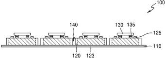
도 1은 예시적인 실시예에 따른 마이크로 광원 어레이의 개략적인 구조를 보이는 단면도이다.1 is a cross-sectional view showing a schematic structure of a micro light source array according to an exemplary embodiment.
마이크로 광원 어레이(100)는 각각 독립적으로 구동되는 복수 개의 서브 픽셀을 포함하는 디스플레이 장치에 채용될 수 있다. 디스플레이 장치에서 서브 픽셀은 서로 다른 칼라 광이 출사되는 단위를 나타낼 수 있다. 예를 들어, 디스플레이 장치는 적색 광을 표시하는 제1 서브 픽셀, 녹색 광을 표시하는 제2 서브 픽셀, 청색 광을 표시하는 제3 서브 픽셀을 포함할 수 있다. 제1 내지 제3 서브 픽셀이 하나의 픽셀을 구성할 수 있다. 픽셀은 예를 들어, 제1 내지 제3 서브 픽셀의 조합에 의해 칼라 영상을 표시할 수 있다. 마이크로 광원 어레이(100)는 베이스(110)에 서브 픽셀에 대응되게 구비된 실리콘 서브 마운트(120)와, 실리콘 서브 마운트(120)에 구비된 구동 회로(123)와, 실리콘 서브 마운트(120)에 결합된 발광 소자 칩(130)을 포함할 수 있다.The micro
이웃하는 실리콘 서브 마운트(120) 사이에 트렌치(140)가 구비되어, 실리콘 서브 마운트(120)가 이격되어 배열될 수 있다. 트렌치(140)는 베이스(110)가 노출되도록 형성될 수 있다. 즉, 실리콘 서브 마운트(120)는 서로 별개의 몸체로 이격되어 있다. 구동 회로(123)는 발광 소자 칩(130)을 구동하기 위한 적어도 하나의 트랜지스터와 적어도 하나의 커패시터를 포함할 수 있다. 구동 회로(123)는 CMOS(complementary metal-oxide semiconductor) 또는 NMOS(n-channel metal-oxide semiconductor)를 포함할 수 있다. 구동 회로(123)는 반도체 공정을 통해 제작될 수 있다. 본 실시예에서 발광 소자 칩(130)은 예를 들어, 청색 광을 출사하는 광원일 수 있다. 디스플레이 장치는 발광 소자 칩(130)에서 출사된 청색 광의 칼라를 변환하는 칼라 변환 소자를 구비하여 칼라 영상을 표시할 수 있다. 이에 대해서는 후술하기로 한다. A
베이스(110)는 본 실시예의 마이크로 광원 어레이(100)가 채용되는 디스플레이 장치의 타켓 기판, 예를 들어 디스플레이 장치의 백플레인(back plane)을 위한 기판일 수 있고, 또는 마이크로 광원을 고정 지지하기 위한 지지판일 수 있다. 또는, 베이스(110)가 마이크로 광원을 타켓 기판에 전사하기 위한 이동부일 수 있다. 베이스(110)는 이 밖에도 다양한 장치에 적용될 수 있다. The base 110 may be a target substrate of a display device to which the micro
도 2는 예시적인 실시예에 따른 마이크로 광원 어레이 제조 방법을 나타낸 것이다.Fig. 2 shows a method of manufacturing a micro light source array according to an exemplary embodiment.
실리콘 기판에 반도체 공정을 통해 구동 회로를 형성할 수 있다(S10). 구동 회로는 앞서 설명한 바와 같이 발광 소자 칩을 구동하기 위한 회로일 수 있다. 그리고, 실리콘 기판에 트렌치를 형성할 수 있다(S20). 여기서, 트렌치는 실기콘 기판을 관통하지 않고 소정 깊이를 가지고 형성될 수 있다. 실리콘 기판에 발광 소자 칩이 배열된 발광 소자 어레이를 본딩한다(S30). 그리고, 실리콘 기판을 후면에서 연마하여 트렌치가 실리콘 기판을 관통하여 형성되도록 한다(S40).A driving circuit may be formed on a silicon substrate through a semiconductor process (S10). The driving circuit may be a circuit for driving the light emitting device chip as described above. Then, a trench may be formed on the silicon substrate (S20). Here, the trench may be formed with a predetermined depth without penetrating the actual cone substrate. A light emitting device array in which light emitting device chips are arranged on a silicon substrate is bonded (S30). Then, the silicon substrate is polished from the rear surface so that the trench is formed through the silicon substrate (S40).
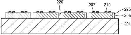
이하에서, 예시적인 마이크로 광원 어레이 제조 방법을 상세히 설명한다. 도 3을 참조하면, 실리콘 기판(201)에 구동 회로(205)를 형성할 수 있다. 구동 회로(205)는 예를 들어, 적어도 하나의 트랜지스터와 적어도 하나의 커패시터를 포함할 수 있다. 또는, 구동 회로(205)는 CMOS(complementary metal-oxide semiconductor) 또는 NMOS(n-channel metal-oxide semiconductor)를 포함할 수 있다. 구동 회로(205)는 반도체 공정을 통해 제작될 수 있다.Hereinafter, a method of manufacturing an exemplary micro light source array will be described in detail. Referring to FIG. 3, a driving
도 4를 참조하면, 구동 회로(205)에 대응하여 컨택 패드(207)가 구비될 수 있다. 컨택 패드(207)는 후술할 디스플레이 장치를 위한 능동 매트릭스 회로와 접속될 수 있다. 컨택 패드(207)은 하나 이상의 층을 포함할 수 있으며, 예를 들어, 금속, 전도성 산화물 및 전도성 중합체들을 포함한 다양한 전도성 재료로 형성될 수 있다. Referring to FIG. 4, a
또한, 구동 회로(205)에 본딩 패드(210)가 구비될 수 있다. 본딩 패드(210)는 후술할 마이크로 광원을 연결하기 위해 구비될 수 있다. In addition, a
도 5를 참조하면, 실리콘 기판(201)에 트렌치(220)를 형성할 수 있다. 트렌치(220)는 예를 들어, 딥 RIE(deep reactive ion etching) 공정을 통해 형성될 수 있다. 트렌치(220)에 의해 서로 이격된 실리콘 서브 마운트(225)가 형성될 수 있다. 트렌치(220)는 실리콘 서브 마운트(225)의 두께를 결정할 수 있다. 예를 들어, 트렌치(220)는 20㎛ 이하의 깊이를 가질 수 있다.Referring to FIG. 5, a
도 6을 참조하면, 기판(231)에 발광 소자 칩(235)을 형성할 수 있다. 발광 소자 칩(235)은 복수 개의 층을 포함할 수 있다. 발광 소자 칩(235)은 예를 들어, 도핑되지 않은(undoped) GaN/n-GaN/MQW(multi quantum well)/p-GnN층을 포함할 수 있다. 하지만, 이는 일 예일 뿐이고 다양한 실시예가 가능하다. 기판(231)은 예를 들어, 사파이어, SiC, Si, GaAs, GaN, ZnO, Si, GaP, InP, Ge, 및 Ga203 중 적어도 어느 하나로 형성될 수 있다. 발광 소자 칩(235)은 하나의 칼라 광을 출사하는 동일한 구조를 가질 수 있다. 발광 소자 칩(235)은 예를 들어, 청색 광을 조사하는 LED일 수 있다. 이와 같이 발광 소자 칩을 하나의 칼라 광을 조사하는 단일 칩으로 구성하는 경우, 발광 소자 칩의 수율을 높일 수 있고, 마이크로 광원의 전사 효율도 높일 수 있다. 다시 말하면, 복수 칼라 광의 발광 소자 칩을 이용하는 경우, 다른 칼라 광의 발광 소자 칩을 각각 제조해야 해야 하므로, 제조 공정이 복잡할 수 있다. 그리고, 다른 칼라 광의 발광 소자 칩을 전사하는 경우, 전사 과정이 칼라 광마다 따로 이루어져야 하므로 전사 효율이 저하된다. 또한, 다른 칼라 광의 발광 소자 칩을 사용하는 경우, 발광 소자 칩의 사이즈가 칼라마다 다를 수 있으므로 발광 소 자 칩을 전사할 때, 피치 간격을 조절하는 것이 어려울 수 있다. 이에 비해, 하나의 칼라 광을 조사하는 발광 소자 칩을 이용하는 경우 전사 과정을 크게 줄일 수 있다. Referring to FIG. 6, a light emitting
도 7을 참조하면, 발광 소자 칩(235)에 전극(240)을 형성할 수 있다. 전극(240)은 알루미늄, 몰리브덴, 티타늄, 텅스텐, 은, 또는 금, 또는 그것의 합금과 같은 금속을 포함할 수 있다. 또는, 전극(240)은 ITO, IZO, ZnO, 또는 In2O3 등의 투명 도전성 산화물(TCO), 카본 나노 튜브 필름 또는 투명한 도전성 폴리머와 같은 도전성 물질을 포함하는 투명 도전층을 포함할 수 있다.Referring to FIG. 7, an
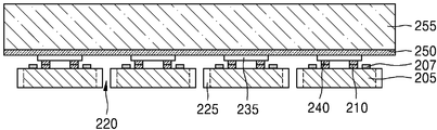
도 8을 참조하면, 기판(231)을 뒤집어서 발광 소자 칩(235)이 도 5에 도시된 실리콘 서브 마운트(225)와 마주보도록 정렬할 수 있다. 그리고, 발광 소자 칩(235)과 실리콘 서브 마운트(225)를 결합할 수 있다. 예를 들어, 발광 소자 칩(235)과 실리콘 서브 마운트(225)는 플립칩 본딩될 수 있다. Referring to FIG. 8, the
도 9를 참조하면, 발광 소자 칩(235)으로부터 기판(231)을 제거한다. 기판(231)은 레이저 리프트 오프(laser lift off) 또는 기계적 리프트 오프(mechanical lift off) 방법에 의해 제거될 수 있다. Referring to FIG. 9, the
그런 다음, 도 10에 도시된 바와 같이, 접착층(250)이 구비된 핸들링 웨이퍼(255)를 도 9에 도시된 발광 소자 칩(235)에 부착할 수 있다. 그리고, 도 11에 도시된 바와 같이 실리콘 기판(201)을 후면에서부터 연마하여 트렌치(220)가 관통하도록 할 수 있다. 그럼으로써, 실리콘 서브 마운트(225)가 서로 분리될 수 있다. 도 12를 참조하면, 실리콘 서브 마운트(225)를 테입(260)에 결합하고, 핸들링 기판(255)을 제거할 수 있다. 테입(260)은 실리콘 서브 마운트(225)들의 배열이 흐트러지지 않도록 고정 지지해 주고, 필요에 따라 쉽게 제거될 수 있는 재질로 형성될 수 있다. 본 실시예에서 실리콘 서브 마운트(225)와, 이에 대응하는 발광 소자 칩(235)을 포함한 구성이 마이크로 광원(265)일 수 있다. 이와 같이 하여, 마이크로 광원 어레이(270)를 제작할 수 있다. Then, as illustrated in FIG. 10, the handling
도 13에 도시된 바와 같이 마이크로 광원 어레이(270)가 베이스(280)에 전사될 수 있다. 마이크로 광원 어레이(270)는 테입(260)에 탑재된 채로 전체가 베이스(280)에 전사될 수 있다. 베이스(280)는 마이크로 광원 어레이(270)가 탑재될 타켓 기판일 수 있다. 이와 같이 마이크로 광원 어레이(270)를 전체적으로 베이스(280)에 전사하고, 마이크로 광원(265)를 원하는 간격으로 벌릴 수 있다. 마이크로 광원(265) 사이의 간격을 벌리는 방법은 다양할 수 있다. As shown in FIG. 13, the micro
도 14를 참조하면, 마이크로 광원 어레이(270)에서는 마이크로 광원(265)이 nХm 매트릭스 형태로 배열될 수 있다. 도 14에서는 마이크로 광원(265)이 5Х5 매트릭스 형태로 배열되어 있다. 도면에서는 편의상 마이크로 광원(265)을 단순하게 사각형으로만 도시하였다. Referring to FIG. 14, in the micro
마이크로 광원 어레이(270)는 제1컬럼(271), 제2컬럼(272), 제3컬럼(273), 제4컬럼(274), 제5컬럼(275)을 포함할 수 있다. 이동 소자(277)를 이용하여 마이크로 광원 어레이(270)의 제1컬럼(271)을 제1방향(예를 들어, X 방향)으로 분리 및 이송시킬 수 있다. 여기서, 제1방향은 마이크로 광원 사이의 간격을 2차원적으로 조절할 때, 어느 한 방향을 나타낼 수 있다. 이어서, 이동 소자(277)를 이용하여 마이크로 광원 어레이(270)의 제2컬럼(272)을 분리 및 이송시킬 수 있다. 동일한 방식으로, 제3컬럼(273), 제4컬럼(274), 제5컬럼(275)을 분리 및 이송시킬 수 있다. 이웃하는 컬럼 사이의 간격은 마이크로 광원 어레이가 적용되는 장치에서 요구하는 규격에 따라 정해질 수 있다. 이와 같이 마이크로 광원 어레이(270)가 한꺼번에 타켓 기판(도 13의 280)에 전사되고, 마이크로 광원(265)들이 컬럼 단위로 분리되므로 마이크로 광원을 효율적으로 전사할 수 있고, 전사 작업 시간을 줄일 수 있다. 도 14에서는 마이크로 광원의 1차원 분리 방법을 설명하고 있다.The micro
도 15는 마이크로 광원의 2차원 분리 방법을 도시한 것이다.15 shows a two-dimensional separation method of a micro light source.
마이크로 광원(265)이 타켓 기판(280)에서 제2방향(예를 들어, Y 방향)으로 분리 및 이송될 수 있다. 여기서, 제2방향은 마이크로 광원 사이의 간격을 2차원적으로 조절할 때, 다른 한 방향을 나타낼 수 있다. 이동 소자(277)를 이용하여 제1로우(row)에 있는 마이크로 광원(265)들을 동시에 제2방향으로 이송시킬 수 있다. 이와 동일한 방식으로 제2로우, 제3로우, 제4로우, 제5로우에 있는 마이크로 광원들을 분리 및 이송시킬 수 있다. 그럼으로써, 도 16에 도시된 바와 같이 타겟 기판(280)에 마이크로 광원(275)들이 정렬될 수 있다.The micro
예를 들어, 100×100 ㎛2 LED를 사용하여 60 PPI(Pixel per Inch)를 구현할 때, 서브 픽셀 사이의 피치가 대략 420㎛일 수 있다. 그러면, LED 광원을 전사할 때, LED 피치 간격을 대략 LED 폭의 4.2배로 벌려주면 60PPI를 구현할 수 있다. 또는, 10×10 ㎛2 LED를 사용하여 568 PPI(Pixel per Inch)를 구현할 때, 서브 픽셀 사이의 피치가 대략 44.8㎛일 수 있다. 그러면, LED 광원을 전사할 때, LED 피치 간격을 대략 LED 폭의 4.4배로 벌려주면 568 PPI를 구현할 수 있다. For example, when implementing 60 pixels per inch (PPI) using 100×100 μm 2 LEDs, the pitch between sub-pixels may be approximately 420 μm. Then, when transferring the LED light source, if the LED pitch interval is approximately 4.2 times the width of the LED, 60 PPI can be realized. Alternatively, when realizing 568 pixels per inch (PPI) using 10×10 μm 2 LEDs, the pitch between sub-pixels may be approximately 44.8 μm. Then, when transferring the LED light source, if the LED pitch interval is approximately 4.4 times the width of the LED, 568 PPI can be realized.
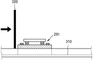
도 17은 마이크로 광원의 전사 방법의 다른 예를 도시한 것이다. 도 18은 도 17의 C-C 선 단면도이다.17 shows another example of a method of transferring a micro light source. 18 is a cross-sectional view taken along line C-C in FIG. 17.
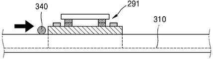
도 17을 참조하면, 마이크로 광원 전사 장치(300)는 마이크로 광원(290)이 일렬로 배열된 1차원 마이크로 광원 어레이(291)가 이동할 수 있는 채널(310)을 포함할 수 있다. 채널(310)은 마이크로 광원 어레이(291)가 초기 배열되는 제1영역(310A), 마이크로 광원 어레이(291)가 이송되는 경로를 포함하는 제2영역(310B), 마이크로 광원(290)이 소정 간격으로 벌어져 정렬되는 제3영역(310C)을 포함할 수 있다.Referring to FIG. 17, the micro light
도 18을 참조하면, 채널(310)은 마이크로 광원 어레이(291)가 가이드되는 그루브를 포함할 수 있다. 1차원 마이크로 광원 어레이(291)가 채널(310)에 수용되어 채널(310)을 따라 이송될 수 있다. Referring to FIG. 18, the
제1영역(310A)은 마이크로 광원 어레이(291)가 이송되기 전에 채널(310)에 안착되는 영역일 수 있다. 제1 영역(310A)에서는 마이크로 광원(290)이 제1방향(Y 방향)으로 제1간격(D1)으로 배열되고, 제2방향(X 방향)으로 제2간격(D2)으로 배열될 수 있다. 제2영역(310B)은 점점 넓어지는 테이퍼 형태를 가질 수 있다. 제2영역(310B)에서는 제1방향(Y 방향)으로 채널(310) 사이 간격이 점점 넓어지도록 구성될 수 있다. 제3영역(310C)에서는 채널(310) 사이 간격이 제3간격(D3)을 가질 수 있다. 제3간격(D3)이 제1간격(D1)보다 클 수 있다. 마이크로 광원 어레이(291)가 제1영역(310A)에서 제3영역(310C)으로 이송되면 마이크로 광원(290) 사이의 간격이 제3간격(D3)으로 조절될 수 있다.The
제1 방향(Y 방향)으로 배열된 첫 번째 라인의 마이크로 광원 어레이를 이동 소자(320)를 이용하여 채널(310)을 따라 한꺼번에 이송할 수 있다. 이동 소자(320)에 의해 제1영역(310A)에서 제3영역(310C)으로 이송된 마이크로 광원 어레이는 마이크로 광원 사이의 간격이 제3간격(D3)으로 증가될 수 있다. 이어서, 제1 방향(Y 방향)으로 배열된 두 번째 라인의 마이크로 광원 어레이를 이동 소자(320)를 이용하여 채널(310)을 따라 한꺼번에 이송할 수 있다. 순서대로 n 번째 마이크로 광원 어레이를 채널을 통해 이송할 수 있다. 도 19를 참조하면, 이와 같이 하여 제1 영역(310A)에 있는 마이크로 광원 어레이를 제3영역(310C)으로 모두 이송하면, 제1 방향(Y 방향)으로의 마이크로 광원(290) 사이의 제3간격(D3)이 제1간격(D1)보다 커지고, 제2방향(X 방향)으로의 마이크로 광원(290) 사이의 제4간격(D4)이 제2간격(D2)보다 커질 수 있다. 다시 말하면, 마이크로 광원 사이의 간격이 2차원적으로 조절될 수 있다.The micro light source array of the first line arranged in the first direction (Y direction) may be transferred along the
도 20 및 도 21은 마이크로 광원 어레이(291)가 이동 소자(320)에 의해 채널(310)을 통해 이동하는 것을 보인 것이다. 이동 소자(320)가 마이크로 광원 어레이(291)를 슬라이딩시킬 수 있는 판일 수 있다.20 and 21 show that the micro
도 22는 한 쌍의 이동 소자(320)(321)를 이용하여 마이크로 광원 어레이(291)를 이송하는 것을 보인 것이다. 22 shows transferring the micro
도 23은 이동 소자(330)가 마이크로 광원 어레이(291)을 양 측에서 잡고 이송시킬 수 있도록 제1부분(330a)과 제2부분(330b)을 포함할 수 있다. 23 may include a first portion 330a and a second portion 330b so that the moving
도 24는 이동 소자(340)가 와이어로 구성된 예를 도시한 것이다. 이동 소자(340)가 마이크로 광원 어레이(291)의 일 측면에 접촉하여 마이크로 광원 어레이(291)를 채널(310)을 통해 슬라이딩시킬 수 있다. 24 shows an example in which the
도 25는 한 쌍의 이동 소자(340)(341)가 마이크로 광원 어레이(291)의 양 측에 구비되어 마이크로 광원 어레이(291)를 이송시킬 수 있다.25, a pair of
도 26은 나란하게 이격되어 배열된 제1, 제2, 제3 및 제4 마이크로 광원 어레이(411)(412)(413)(414)의 간격을 조절하는 이동 소자(420)를 도시한 것이다. 이동 소자(420)는 쐐기형 구조를 가질 수 있다. 이동 소자(420)는 각 마이크로 광원 어레이 사이로 진입하는 제1부분(420a)과 일정한 폭을 가지는 제2부분(420b)을 포함할 수 있다. 제1부분(420a)은 쐐기형으로 되어 있어 이웃하는 마이크로 광원 어레이 사이로 용이하게 진입할 수 있다. 그리고, 제1부분(420a)의 폭이 점점 증가하는 형태를 가지므로 이동 소자(420)가 마이크로 광원 어레이 사이로 진행함에 따라 마이크로 광원 어레이 사이 간격이 점점 벌어진다. FIG. 26 shows the
그리고, 도 27에 도시된 바와 같이 이동 소자(420)의 제2부분(420b)이 마이크로 광원 어레이 사이로 진입함에 따라 제2부분(420b)의 폭(W1)만큼 마이크로 광원 어레이 사이가 벌어질 수 있다. 마이크로 광원 어레이 사이의 간격은 제2부분(420b)의 폭(W1)에 의해 결정될 수 있다. 복수 개의 이동 소자(420)가 동시에 마이크로 광원 어레이 사이로 진입할 때, 복수 개의 마이크로 광원 어레이가 일정한 간격 W1으로 배열될 수 있다. 이 경우에는 마이크로 광원 어레이가 도면 상 X 방향의 1차원적으로 간격 조절이 이루어질 수 있다.Then, as shown in FIG. 27, as the
도 28은 상술한 바와 같이 마이크로 광원의 전사가 이루어진 상태에서 트렌치(140)에 필름 막(450)이 형성되어 평탄화된 것을 보인 것이다. 도 28에서 도 1과 동일한 참조 번호를 사용한 구성 요소는 도 1에서 설명한 것과 실질적으로 동일하므로 여기서는 상세한 설명을 생략한다.28 shows that the
도 29를 참조하면, 필름 막(450)에 배선(460)이 형성될 수 있다. 배선(460)이 컨택 패드(125)에 연결될 수 있다. Referring to FIG. 29, a
도 30은 일 실시예에 따른 디스플레이 장치(400)를 도시한 것이다.30 illustrates a
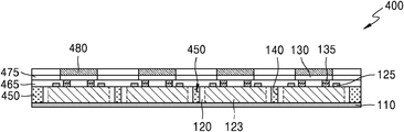
디스플레이 장치(400)는 제1 칼라 광을 표시하는 제1 서브 픽셀, 제2 칼라 광을 표시하는 제2 서브 픽셀, 제3 칼라 광을 표시하는 제3 서브 픽셀을 포함할 수 있다. 제1 내지 제3 서브 픽셀이 하나의 픽셀을 구성할 수 있다. 베이스(110)에 각 서브 픽셀에 대응되게 구비된 실리콘 서브 마운트(120)와, 실리콘 서브 마운트(120)에 구비된 구동 회로(123)와, 실리콘 서브 마운트(120)에 결합된 발광 소자 칩(130)을 포함할 수 있다. The
이웃하는 실리콘 서브 마운트(120) 사이에 트렌치(140)가 구비되어, 실리콘 서브 마운트(120)가 이격되게 배열될 수 있다. 트렌치(140)는 베이스(110)가 노출되도록 형성될 수 있다. 즉, 실리콘 서브 마운트(120)는 서로 별개의 몸체로 이격되어 있다. 구동 회로(123)는 발광 소자 칩(130)을 구동하기 위한 적어도 하나의 트랜지스터와 적어도 하나의 커패시터를 포함할 수 있다. 구동 회로(123)는 CMOS(complementary metal-oxide semiconductor) 또는 NMOS(n-channel metal-oxide semiconductor)를 포함할 수 있다. 본 실시예에서 발광 소자 칩(130)은 예를 들어, 청색 광을 출사하는 광원일 수 있다. 디스플레이 장치(400)는 발광 소자 칩(130)에서 출사된 청색 광의 칼라를 변환하는 칼라 변환 소자(480)를 구비하여 칼라 영상을 표시할 수 있다.A
도 30을 참조하면, 서브 마운트(120)에 적어도 하나의 층(465)이 구비될 수 있다. 예를 들어, 적어도 하나의 층(465)은 평탄화 층 또는 절연층일 수 있다. 적어도 하나의 층(465)에 배선이 더 구비될 수 있다. 또한, 적어도 하나의 층(465) 위에 블랙 매트릭스 필름(475)이 구비될 수 있다. 블랙 매트릭스 필름(475)은 발광 소자 칩(130)에서 나오는 광이 이웃하는 서브 픽셀로 혼합되는 것을 방지할 수 있다. 발광 소자 칩(130)에 칼라 변환 소자(480)가 구비될 수 있다. 칼라 변환 소자(480)는 예를 들어, 양자점 칼라 필터일 수 있다. 칼라 변화 소자(480)는 발광 소자 칩(130)에서 나오는 광의 파장을 선택적으로 전환할 수 있다. 예를 들어, 발광 소자 칩(130)은 청색 광을 출사할 수 있다. 발광 소자 칩(130)에서 나온 청색 광을 칼라 변환 소자(480)가 적색 광으로 전환하거나, 녹색 광으로 전환할 수 있다. 예를 들어, 양자점 칼라 필터의 경우, 양자점들은 원자가 수 백 개 내지 수 천 개 이상 모인 입자들로, 양자(quantum)를 나노미터(nm)의 단위로 합성시킨 반도체 결정일 수 있다. 예를 들어, 양자점들은 II-VI족, III-V족, IV-VI족, IV족 반도체 화합물 및 이들의 혼합물로 형성될 수 있다. 예를 들어, 양자점은 CdS, CdSe, CdTe, ZnS, ZnSe, ZnTe, InP, InAs 또는 및 이들의 혼합물로 이루어진 군에서 선택하여 형성될 수 있다. 양자점들은 광이 입사되면 입자의 크기에 따라 다양한 색을 나타낼 수 있다. 발광 소자 칩(130)에서 발광된 청색 광을 그대로 통과시키거나, 녹색 광으로 변환시키거나 적색 광으로 변환시킬 수 있다. 그럼으로써, 칼라 영상을 표시할 수 있다. Referring to FIG. 30, at least one layer 465 may be provided on the sub-mount 120. For example, the at least one layer 465 may be a planarization layer or an insulating layer. Wiring may be further provided on the at least one layer 465. Also, a
도 31은 다른 실시예에 따른 디스플레이 제조 방법을 나타낸 것이다. 제조 방법은 실리콘 서브 마운트를 제작하는 단계를 포함한다(S110). 실리콘 서브 마운트는 도 3 내지 도 5를 참조하여 설명한 방법에 따라 제작될 수 있다. 다음, 발광 소자 칩을 실리콘 서브 마운트에 본딩할 수 있다(S120). 다음, 발광 소자 칩치 본딩된 실리콘 서브 마운트를 분리할 수 있다(S130). 그리고, 분리된 실리콘 서브 마운트를 타겟 기판에 피치를 늘리면서 전사시킬 수 있다(S140). 예를 들어, 타겟 기판에는 데이터 라인(data line), 스캔 라인(scan line), VDD 등이 프린팅될 수 있다. 그리고, 실리콘 서브 마운트와 발광 소자 칩을 서로 전기적으로 연결하는 배선 작업을 할 수 있다(S180). 31 illustrates a display manufacturing method according to another embodiment. The manufacturing method includes manufacturing a silicon sub-mount (S110). The silicon sub-mount can be manufactured according to the method described with reference to FIGS. 3 to 5. Next, the light emitting device chip may be bonded to the silicon sub-mount (S120). Next, the silicon sub-mount bonded with the light-emitting device chip may be separated (S130 ). Then, the separated silicon sub-mount may be transferred to the target substrate while increasing the pitch (S140). For example, a data line, a scan line, and VDD may be printed on the target substrate. Further, a wiring operation in which the silicon sub-mount and the light emitting element chip are electrically connected to each other may be performed (S180).
도 32는 다른 실시예에 따른 디스플레이 제조 방법을 나타낸 것이다. 도 32는 도 31과 비교할 때, 단계 S140과 단계 S180 사이에 몇 개의 단계가 더 추가될 수 있다. 실리콘 서브 마운트를 임시 기판에 피치를 늘리면서 전사시킬 수 있다(S140). 그리고, 실리콘 서브 마운트에 경화성 물질을 도포하고 경화시켜 늘어난 피치 상태를 고정시킬 수 있다(S150). 경화된 필름을 임시 기판으로부터 박리한다(S160). 경화된 필름에는 실리콘 서브 마운트와 발광 소자 칩이 배열되어 있다. 타겟 기판에 경화된 필름을 라미네이션 한다(S170). 다음, 실리콘 서브 마운트를 서로 전기적으로 연결하는 배선 작업을 한다(S180). 배선은 예를 들어, 스크린 프린팅 방법, 잉크젯 프린팅 방법 등에 의해 형성될 수 있다. 이와 같이 하여 2차원 픽셀이 전기적으로 연결된 액티브 매트릭스 어레이가 구비될 수 있다.32 illustrates a display manufacturing method according to another embodiment. 32, several steps may be added between steps S140 and S180 when compared to FIG. 31. The silicon sub-mount can be transferred to the temporary substrate while increasing the pitch (S140). Then, the cured material is applied to the silicone sub-mount and cured to fix the stretched pitch state (S150). The cured film is peeled from the temporary substrate (S160). In the cured film, a silicon sub-mount and a light emitting device chip are arranged. The cured film is laminated to the target substrate (S170). Next, wiring is performed to electrically connect the silicon sub-mounts to each other (S180). The wiring can be formed by, for example, a screen printing method, an inkjet printing method, or the like. In this way, an active matrix array in which two-dimensional pixels are electrically connected may be provided.
본 발명은 도면에 도시된 실시예를 참고로 설명되었으나 이는 예시적인 것에 불과하며, 당해 기술 분야에서 통상의 지식을 가진 자라면 이로부터 다양한 변형 및 균등한 다른 실시예가 가능하다는 점을 이해할 것이다. 따라서, 본 발명의 진정한 기술적 보호 범위는 첨부된 특허청구범위의 기술적 사상에 의하여 정해져야 할 것이다.The present invention has been described with reference to the embodiments shown in the drawings, but these are merely exemplary, and those skilled in the art will understand that various modifications and equivalent other embodiments are possible therefrom. Therefore, the true technical protection scope of the present invention should be determined by the technical spirit of the appended claims.
100,270: 마이크로 광원 어레이, 110:베이스
120,225: 실리콘 서브 마운트, 123,205:구동 회로
125,207:컨택 패드, 135,210:본딩 패드
130,235:발광 소자 칩, 201:실리콘 기판
265:마이크로 광원,
277,320,321,330,340,341:이동 소자
400:디스플레이 장치
460:액티브 매트릭스 회로
480:칼라 변화 소자 100,270: micro light source array, 110: base
120,225: silicon sub-mount, 123,205: drive circuit
125,207: contact pad, 135,210: bonding pad
130,235: light-emitting element chip, 201: silicon substrate
265: micro light source,
277,320,321,330,340,341:Moving element
400: display device
460: active matrix circuit
480: color change element
Claims (22)
기판에 상기 서브 픽셀에 대응하여 구비되고, 트렌치에 의해 서로 이격되어 배열된 실리콘 서브 마운트;
상기 실리콘 서브 마운트에 결합된 발광 소자 칩; 및
상기 실리콘 서브 마운트에 구비된 구동 회로;를 포함하는 마이크로 광원 어레이.In the micro light source array of the display device including a plurality of sub-pixels that are each driven independently,
A silicon sub-mount provided on the substrate corresponding to the sub-pixels and spaced apart from each other by a trench;
A light emitting device chip coupled to the silicon sub-mount; And
A micro light source array comprising; a driving circuit provided in the silicon sub-mount.
상기 구동 회로가 CMOS 또는 NMOS를 포함하는 광원 어레이.According to claim 1,
The light source array in which the driving circuit comprises CMOS or NMOS.
상기 실리콘 서브 마운트와 전기적으로 연결되는 배선을 더 포함하는 마이크로 광원 어레이.According to claim 1,
The micro light source array further comprises a wiring electrically connected to the silicon sub-mount.
상기 발광 소자 칩이 상기 실리콘 서브 마운트에 플립칩 본딩된 광원 어레이.According to claim 1,
A light source array in which the light emitting device chip is flip-chip bonded to the silicon sub-mount.
상기 이웃하는 실리콘 서브 마운트들이 가로 방향과 세로 방향에 대해 각각 상기 서브 픽셀의 피치 간격으로 이격되어 배치된 마이크로 광원 어레이. According to claim 1,
The neighboring silicon sub-mounts are arranged at a distance between the sub-pixel pitch in the horizontal direction and the vertical direction, respectively.
상기 발광 소자 칩은 마이크로 LED를 포함하는 마이크로 광원 어레이.According to claim 1,
The light emitting device chip is a micro light source array comprising a micro LED.
상기 발광 소자 칩은 청색 광을 발광하는 마이크로 광원 어레이.According to claim 1,
The light emitting device chip is a micro light source array that emits blue light.
기판;
상기 기판에 상기 서브 픽셀에 대응하여 구비되고, 트렌치에 의해 서로 이격되어 배열된 실리콘 서브 마운트;
상기 실리콘 서브 마운트에 결합된 발광 소자 칩;
상기 실리콘 서브 마운트에 구비된 구동 회로; 및
상기 발광 소자 칩 상에 구비되어 상기 발광 소자 칩으로부터 출사된 광의 칼라를 변환하는 칼라 변환 소자;를 포함하는 디스플레이 장치.In the display device including a plurality of sub-pixels are each driven independently,
Board;
A silicon sub-mount provided on the substrate corresponding to the sub-pixel and arranged spaced apart from each other by a trench;
A light emitting device chip coupled to the silicon sub-mount;
A driving circuit provided in the silicon sub-mount; And
And a color conversion element provided on the light emitting element chip to convert the color of light emitted from the light emitting element chip.
상기 구동 회로가 CMOS 또는 NMOS를 포함하는 디스플레이 장치.The method of claim 8,
A display device in which the driving circuit comprises CMOS or NMOS.
상기 발광 소자 칩이 상기 실리콘 서브 마운트에 플립칩 본딩된 디스플레이 장치.The method of claim 8,
A display device in which the light emitting device chip is flip-chip bonded to the silicon sub-mount.
상기 이웃하는 실리콘 서브 마운트들이 가로 방향과 세로 방향에 대해 각각 상기 서브 픽셀의 피치 간격으로 이격되어 배치된 디스플레이 장치. The method of claim 8,
A display device in which the neighboring silicon sub-mounts are spaced apart at a pitch interval of the sub-pixels, respectively, in a horizontal direction and a vertical direction.
상기 발광 소자 칩은 마이크로 LED를 포함하는 디스플레이 장치.The method of claim 8,
The light emitting device chip is a display device comprising a micro LED.
상기 발광 소자 칩은 청색 광을 발광하는 디스플레이 장치.The method of claim 8,
The light emitting device chip is a display device that emits blue light.
상기 실리콘 기판에 트렌치를 형성하는 단계;
상기 실리콘 기판에 발광 소자 어레이를 본딩하는 단계; 및
상기 실리콘 기판을 후면에서 상기 트렌치가 관통되도록 연마하여 서로 이격된 실리콘 서브 마운트를 형성하는 단계;를 포함하는 디스플레이 제조 방법.Forming a driving circuit on the silicon substrate;
Forming a trench in the silicon substrate;
Bonding a light emitting device array to the silicon substrate; And
And polishing the silicon substrate so that the trench is penetrated from the rear to form silicon sub-mounts spaced apart from each other.
상기 서로 이격된 실리콘 서브 마운트를 타켓 기판에 전사하는 단계를 더 포함하는 디스플레이 제조 방법.The method of claim 14,
And transferring the silicon submounts spaced apart from each other to a target substrate.
상기 서로 이격된 실리콘 서브 마운트 사이의 가로 방향과 세로 방향 중 어느 한 방향으로 이동 소자를 삽입하고, 실리콘 서브 마운트 사이를 벌려 정렬하는 단계를 포함하는 디스플레이 제조 방법.The method of claim 14,
And inserting a moving element in either a horizontal direction or a vertical direction between the silicon sub-mounts spaced apart from each other, and aligning the silicon sub-mounts.
상기 실리콘 서브 마운트의 세로 방향과 가로 방향 중 다른 한 방향으로 이동 소자를 삽입하고, 실리콘 서브 마운트 사이를 벌려 정렬하는 단계를 포함하는 디스플레이 제조 방법. The method of claim 16,
A method of manufacturing a display, comprising inserting a moving element in one of a vertical direction and a horizontal direction of the silicon sub-mount and aligning the silicon sub-mounts.
상기 서로 이격된 실리콘 서브 마운트 사이의 제1 방향으로 이동 소자를 삽입하여 분리하는 단계를 포함하는 디스플레이 제조 방법.The method of claim 14,
And inserting and separating a moving element in a first direction between the silicon sub-mounts spaced apart from each other.
상기 제1 방향으로 분리된 실리콘 서브 마운트들의 제2 방향으로 이동 소자를 삽입하고, 그루브를 포함하는 채널을 따라 상기 실리콘 서브 마운트를 이동시키는 단계를 포함하는 디스플레이 제조 방법.The method of claim 18,
And inserting a moving element in a second direction of the silicon sub-mounts separated in the first direction, and moving the silicon sub-mount along a channel including a groove.
상기 채널이 상기 그루브의 간격이 점점 커지는 영역을 포함하는 디스플레이 제조 방법.The method of claim 19,
A method of manufacturing a display, wherein the channel includes an area where the spacing of the grooves gradually increases.
상기 이동 소자가 쐐기형 블레이드를 포함하고, 상기 서로 이격된 실리콘 마운트 사이로 쐐기형 블레이드를 삽입하고 이동시켜 실리콘 서브 마운트 사이를 벌리는 단계를 포함하는 디스플레이 제조 방법. The method of claim 14,
And wherein the moving element includes a wedge-shaped blade, and inserts and moves the wedge-shaped blade between the spaced apart silicon mounts to spread between the silicon sub-mounts.
상기 쐐기형 블레이드가 상기 서로 이격된 실리콘 서브 마운트 사이로 진입하는 제1부분과, 상기 실리콘 서브 마운트 사이의 간격을 조절하는 제2부분을 포함하고, 상기 제2부분의 폭에 따라 실리콘 서브 마운트 사이의 피치 간격이 결정되는 디스플레이 제조 방법.The method of claim 21,
The wedge-shaped blade includes a first portion that enters between the silicon sub-mounts spaced apart from each other, and a second portion that adjusts the distance between the silicon sub-mounts, and between the silicon sub-mounts according to the width of the second portion. A method of manufacturing a display in which pitch spacing is determined.
Priority Applications (3)
| Application Number | Priority Date | Filing Date | Title |
|---|---|---|---|
| KR1020180148546A KR20200062762A (en) | 2018-11-27 | 2018-11-27 | Micro light source array, display device having the same and method of manufacturing display device |
| US16/670,457 US11056473B2 (en) | 2018-11-27 | 2019-10-31 | Micro light source array, display device having the same, and method of manufacturing display device |
| US17/338,748 US11652093B2 (en) | 2018-11-27 | 2021-06-04 | Micro light source array, display device having the same, and method of manufacturing display device |
Applications Claiming Priority (1)
| Application Number | Priority Date | Filing Date | Title |
|---|---|---|---|
| KR1020180148546A KR20200062762A (en) | 2018-11-27 | 2018-11-27 | Micro light source array, display device having the same and method of manufacturing display device |
Publications (1)
| Publication Number | Publication Date |
|---|---|
| KR20200062762A true KR20200062762A (en) | 2020-06-04 |
Family
ID=70771759
Family Applications (1)
| Application Number | Title | Priority Date | Filing Date |
|---|---|---|---|
| KR1020180148546A KR20200062762A (en) | 2018-11-27 | 2018-11-27 | Micro light source array, display device having the same and method of manufacturing display device |
Country Status (2)
| Country | Link |
|---|---|
| US (2) | US11056473B2 (en) |
| KR (1) | KR20200062762A (en) |
Cited By (1)
| Publication number | Priority date | Publication date | Assignee | Title |
|---|---|---|---|---|
| EP4145512A1 (en) * | 2021-09-03 | 2023-03-08 | LG Display Co., Ltd. | Display device |
Family Cites Families (10)
| Publication number | Priority date | Publication date | Assignee | Title |
|---|---|---|---|---|
| JP3682584B2 (en) | 2001-08-06 | 2005-08-10 | ソニー株式会社 | Method for mounting light emitting element and method for manufacturing image display device |
| US7964888B2 (en) * | 2007-04-18 | 2011-06-21 | Cree, Inc. | Semiconductor light emitting device packages and methods |
| DE102009033915B4 (en) | 2009-07-20 | 2022-05-25 | OSRAM Opto Semiconductors Gesellschaft mit beschränkter Haftung | Method of manufacturing a lighting device and lighting device |
| WO2011071559A1 (en) | 2009-12-09 | 2011-06-16 | Nano And Advanced Materials Institute Limited | Method for manufacturing a monolithic led micro-display on an active matrix panel using flip-chip technology and display apparatus having the monolithic led micro-display |
| US9871345B2 (en) * | 2015-06-09 | 2018-01-16 | X-Celeprint Limited | Crystalline color-conversion device |
| KR102617466B1 (en) | 2016-07-18 | 2023-12-26 | 주식회사 루멘스 | Micro led array display apparatus |
| US10475876B2 (en) | 2016-07-26 | 2019-11-12 | X-Celeprint Limited | Devices with a single metal layer |
| WO2019031183A1 (en) * | 2017-08-10 | 2019-02-14 | シャープ株式会社 | Semiconductor module, display device and method for producing semiconductor module |
| US10903267B2 (en) * | 2019-04-04 | 2021-01-26 | Bor-Jen Wu | System and method for making micro LED display |
| US20210013367A1 (en) * | 2019-04-04 | 2021-01-14 | Bor-Jen Wu | System and Method for Making Micro LED Display |
-
2018
- 2018-11-27 KR KR1020180148546A patent/KR20200062762A/en not_active Application Discontinuation
-
2019
- 2019-10-31 US US16/670,457 patent/US11056473B2/en active Active
-
2021
- 2021-06-04 US US17/338,748 patent/US11652093B2/en active Active
Cited By (1)
| Publication number | Priority date | Publication date | Assignee | Title |
|---|---|---|---|---|
| EP4145512A1 (en) * | 2021-09-03 | 2023-03-08 | LG Display Co., Ltd. | Display device |
Also Published As
| Publication number | Publication date |
|---|---|
| US11056473B2 (en) | 2021-07-06 |
| US11652093B2 (en) | 2023-05-16 |
| US20200168594A1 (en) | 2020-05-28 |
| US20210296296A1 (en) | 2021-09-23 |
Similar Documents
| Publication | Publication Date | Title |
|---|---|---|
| US20200258939A1 (en) | Light emitting diode module, display panel having the same and method of manufacturing the same | |
| US11575067B2 (en) | Display substrate, display apparatus, and manufacturing method for display substrate | |
| US10096647B2 (en) | Display apparatus having a plurality of reflective electrodes | |
| US10332949B2 (en) | Display apparatus | |
| TWI663749B (en) | Light emitting apparatus and manufacturing method thereof | |
| KR102413460B1 (en) | Semiconducting pixel, matrix of such pixels, semiconducting structure for the production of such pixels and their methods of fabrication | |
| CN110071202B (en) | Micro LED element and image display element | |
| EP3486946A1 (en) | Growth substrate including micro-light emitting diode chips and method of manufacturing light emitting diode display using the same | |
| KR102579645B1 (en) | Method of transferring semiconductor device, semiconductor device carrier, and method of fabricating display panel | |
| TW201826516A (en) | Micro light-emitting diode chip | |
| US20230387179A1 (en) | Light emitting device for display and display apparatus having the same | |
| KR20210116456A (en) | Light emitting element transfer method for display and display device | |
| US20230005888A1 (en) | Semiconductor light-emitting element supply device and supply method | |
| KR20190115838A (en) | Display appartus using one chip type led and fabrication method of the same | |
| KR102054951B1 (en) | Display apparatus and method for manufacturing sub micro light emitting diode display | |
| US11652093B2 (en) | Micro light source array, display device having the same, and method of manufacturing display device | |
| KR20190112916A (en) | Display apparatus and method for manufacturing thereof | |
| WO2021148895A1 (en) | Light processing device array and method for manufacturing thereof | |
| KR102073572B1 (en) | Display apparatus and method for manufacturing thereof | |
| JP2018529234A (en) | Light emitting device and method for manufacturing light emitting device | |
| KR20180016101A (en) | Method of fabricating display device | |
| US11843077B2 (en) | Unit pixel having light emitting device and displaying apparatus | |
| US20210376188A1 (en) | Method for transferring a light emitting device for display | |
| US11476390B2 (en) | III-V light emitting device with pixels enabling lower cost through-layer vias | |
| CN110993761A (en) | Active matrix colour display device |
Legal Events
| Date | Code | Title | Description |
|---|---|---|---|
| E902 | Notification of reason for refusal |