KR20110120233A - Optical device, analyzer and spectroscopy method - Google Patents
Optical device, analyzer and spectroscopy method Download PDFInfo
- Publication number
- KR20110120233A KR20110120233A KR20110039320A KR20110039320A KR20110120233A KR 20110120233 A KR20110120233 A KR 20110120233A KR 20110039320 A KR20110039320 A KR 20110039320A KR 20110039320 A KR20110039320 A KR 20110039320A KR 20110120233 A KR20110120233 A KR 20110120233A
- Authority
- KR
- South Korea
- Prior art keywords
- wavelength
- resonance peak
- light
- incident
- peak wavelength
- Prior art date
Links
Images


Classifications
-
- G—PHYSICS
- G01—MEASURING; TESTING
- G01N—INVESTIGATING OR ANALYSING MATERIALS BY DETERMINING THEIR CHEMICAL OR PHYSICAL PROPERTIES
- G01N21/00—Investigating or analysing materials by the use of optical means, i.e. using sub-millimetre waves, infrared, visible or ultraviolet light
- G01N21/17—Systems in which incident light is modified in accordance with the properties of the material investigated
- G01N21/25—Colour; Spectral properties, i.e. comparison of effect of material on the light at two or more different wavelengths or wavelength bands
- G01N21/27—Colour; Spectral properties, i.e. comparison of effect of material on the light at two or more different wavelengths or wavelength bands using photo-electric detection ; circuits for computing concentration
-
- G—PHYSICS
- G01—MEASURING; TESTING
- G01N—INVESTIGATING OR ANALYSING MATERIALS BY DETERMINING THEIR CHEMICAL OR PHYSICAL PROPERTIES
- G01N21/00—Investigating or analysing materials by the use of optical means, i.e. using sub-millimetre waves, infrared, visible or ultraviolet light
- G01N21/62—Systems in which the material investigated is excited whereby it emits light or causes a change in wavelength of the incident light
- G01N21/63—Systems in which the material investigated is excited whereby it emits light or causes a change in wavelength of the incident light optically excited
- G01N21/65—Raman scattering
- G01N21/658—Raman scattering enhancement Raman, e.g. surface plasmons
-
- G—PHYSICS
- G01—MEASURING; TESTING
- G01N—INVESTIGATING OR ANALYSING MATERIALS BY DETERMINING THEIR CHEMICAL OR PHYSICAL PROPERTIES
- G01N21/00—Investigating or analysing materials by the use of optical means, i.e. using sub-millimetre waves, infrared, visible or ultraviolet light
- G01N21/17—Systems in which incident light is modified in accordance with the properties of the material investigated
- G01N21/55—Specular reflectivity
- G01N21/552—Attenuated total reflection
- G01N21/553—Attenuated total reflection and using surface plasmons
- G01N21/554—Attenuated total reflection and using surface plasmons detecting the surface plasmon resonance of nanostructured metals, e.g. localised surface plasmon resonance
-
- G—PHYSICS
- G01—MEASURING; TESTING
- G01N—INVESTIGATING OR ANALYSING MATERIALS BY DETERMINING THEIR CHEMICAL OR PHYSICAL PROPERTIES
- G01N21/00—Investigating or analysing materials by the use of optical means, i.e. using sub-millimetre waves, infrared, visible or ultraviolet light
- G01N21/62—Systems in which the material investigated is excited whereby it emits light or causes a change in wavelength of the incident light
- G01N21/63—Systems in which the material investigated is excited whereby it emits light or causes a change in wavelength of the incident light optically excited
- G01N21/65—Raman scattering
Abstract
Description
본 발명은 광 디바이스, 분석 장치 및 분광 방법 등에 관한 것이다.
The present invention relates to optical devices, analytical devices, spectroscopic methods and the like.
최근, 의료 진단이나 음식물의 검사 등에 이용되는 센서의 수요가 증대하고 있어, 고감도 또한 소형의 센서의 개발이 요구되고 있다. 이러한 요구에 응하기 위해서, 전기화학적인 수법을 비롯하여 다양한 타입의 센서가 검토되고 있다. 이들 중에서, 집적화가 가능하다는 점, 저비용, 측정 환경을 가리지 않다는 점 등의 이유로부터, 표면 플라즈몬 공명을 이용한 센서에 관한 관심이 높아지고 있다. In recent years, the demand of the sensor used for a medical diagnosis, food inspection, etc. is increasing, and the development of a highly sensitive and small sensor is calculated | required. In order to meet these demands, various types of sensors have been examined, including electrochemical techniques. Among these, the interest regarding the sensor using surface plasmon resonance is increasing from the reason that integration is possible, a low cost, and a choice of a measurement environment.
예컨대, 특허 문헌 1에는, 표면에 금속 미립자가 고정된 기판에 의한 국재 표면 플라즈몬 공명(localized surface plasmon resonance)을 이용하여, 센서 감도를 향상시키는 수법이 개시되어 있다.
For example,
표면 플라즈몬 공명에 의한 전장(電場) 증강을 이용해서 라만 산란의 강도를 증강시켜서, 표적물의 센싱 감도를 향상시키는 경우, 그 전장 증강도는, 여기 파장에 있어서의 전장 증강도와 라만 산란 파장에 있어서의 전장 증강도의 곱에 의해 결정된다. 따라서, 센싱의 고감도화를 위해서는, 여기 파장에 있어서의 전장 증강도와 라만 산란 파장에 있어서의 전장 증강도를 함께 향상시킬 필요가 있다. When the intensity of the Raman scattering is enhanced by using the electric field enhancement by surface plasmon resonance to improve the sensing sensitivity of the target, the electric field enhancement degree is obtained by the electric field enhancement at the excitation wavelength and the Raman scattering wavelength. It is determined by the product of the full-length buildup. Therefore, in order to increase the sensitivity, it is necessary to improve both the electric field enhancement in the excitation wavelength and the electric field enhancement in the Raman scattering wavelength.
예컨대, 상술한 특허 문헌 1의 수법에서는, 금속 미립자의 크기나 배열을 균일하게 하는 것이 곤란하기 때문에, 공명 파장에도 편차가 생겨서, 흡광도 스펙트럼의 폭이 넓어지게 된다. 또한, 공명 피크도 하나밖에 생기지 않는다. 이 때문에, 예컨대 희박한 표적물을 센싱하는 용도로서는, 여기 파장과 라만 산란 파장 양 파장에 있어서 충분한 전장 증강도를 얻는 것이 곤란하게 되어 버린다. For example, in the above-described method of
한편, 특허 문헌 2에는, 장파장측으로 시프트하는 공명 피크와 단파장측으로 시프트하는 공명 피크를 갖는 국재 플라즈몬 공명 센서의 기술이 개시되어 있다. 또한, 특허 문헌 3에는, 복수의 파장에 대해 공진 가능하게 하기 위해서 복수의 공진 영역에 의해 미소 공진기가 구성된 전장 증강 디바이스의 기술이 개시되어 있다. On the other hand, Patent Document 2 discloses a technique of a local plasmon resonance sensor having a resonance peak shifting to a long wavelength side and a resonance peak shifting to a short wavelength side. In addition, Patent Document 3 discloses a technique of an electric field enhancement device in which a micro-resonator is constituted by a plurality of resonance regions in order to enable resonance with a plurality of wavelengths.
본 발명의 몇 가지 측면에 따르면, 여기 파장에 있어서의 전장 증강도와 라만 산란 파장에 있어서의 전장 증강도를 향상시킬 수 있는 광 디바이스, 분석 장치 및 분광 방법 등을 제공할 수 있다.
According to some aspects of the present invention, there can be provided an optical device, an analytical device, a spectroscopic method, and the like, which can improve the electric field enhancement in the excitation wavelength and the electric field enhancement in the Raman scattering wavelength.
본 발명의 일 측면은, 전기 전도체의 돌기를 가상 평면에 대하여 평행한 방향을 따라 제 1 주기로 배열한 제 1 돌기군을 갖고, 상기 가상 평면을 향하는 수직선에 대하여 경사진 방향으로 진행하는 광을 상기 제 1 주기로 배열된 상기 제 1 돌기군에 입사시킨 경우의 표면 플라즈몬 공명이, 제 1 공명 피크 파장과 제 2 공명 피크 파장 각각으로 발생하고, 상기 제 1 공명 피크 파장을 포함하는 제 1 공명 피크 파장 대역은, 상기 표면 증강 라만 산란에 있어서의 여기 파장 λ1을 포함하고, 상기 제 2 공명 피크 파장을 포함하는 제 2 공명 피크 파장 대역은, 상기 표면 증강 라만 산란에 있어서의 라만 산란 파장 λ2를 포함하는 광 디바이스에 관한 것이다. One aspect of the present invention has a first projection group in which protrusions of an electrical conductor are arranged in a first period along a direction parallel to an imaginary plane, wherein the light propagates in a direction inclined with respect to a vertical line facing the imaginary plane. Surface plasmon resonance when incident on the first projection group arranged in a first period occurs at a first resonance peak wavelength and a second resonance peak wavelength, respectively, and includes a first resonance peak wavelength including the first resonance peak wavelength. The band includes an
본 발명의 일 측면에 따르면, 제 1 돌기군의 전기 전도체의 돌기가 가상 평면에 대하여 평행한 방향을 따라서 제 1 주기로 배열된다. 이 제 1 주기로 배열된 제 1 돌기군에는 가상 평면을 향하는 수직선에 대하여 경사진 방향으로 진행하는 광이 입사된다. 이 입사된 광에 의해, 제 1 공명 피크 파장과 제 2 공명 피크 파장의 각각으로 표면 플라즈몬 공명이 발생한다. 이 때, 제 1 공명 피크 파장을 포함하는 제 1 공명 피크 파장 대역에는, 표면 증강 라만 산란에 있어서의 여기 파장 λ1이 포함되고, 제 2 공명 피크 파장을 포함하는 제 2 공명 피크 파장 대역에는, 표면 증강 라만 산란에 있어서의 라만 산란 파장 λ2이 포함되도록, 제 1 주기와 광의 입사 각도가 설정된다. 이로써, 여기 파장에 있어서의 전장 증강도와 라만 산란 파장에 있어서의 전장 증강도를 향상시키는 것 등이 가능하게 된다. According to one aspect of the invention, the projections of the electrical conductors of the first projection group are arranged in a first period along a direction parallel to the virtual plane. Light traveling in the direction inclined with respect to the vertical line toward the imaginary plane is incident on the first projection group arranged at the first period. By this incident light, surface plasmon resonance occurs at each of the first resonance peak wavelength and the second resonance peak wavelength. At this time, the excitation wavelength? 1 in the surface enhancement Raman scattering is included in the first resonance peak wavelength band including the first resonance peak wavelength, and the surface is included in the second resonance peak wavelength band including the second resonance peak wavelength. The first period and the angle of incidence of the light are set so that the Raman scattering wavelength lambda 2 in the enhanced Raman scattering is included. Thereby, it becomes possible to improve the electric field enhancement in the excitation wavelength and the electric field enhancement in the Raman scattering wavelength.
또한, 본 발명의 일 측면에서는, 상기 라만 산란 파장 λ2는, 상기 여기 파장 λ1보다 긴 파장이어도 된다. In addition, in one aspect of the present invention, the Raman scattering wavelength λ 2 may be a wavelength longer than the
이와 같이 하면, 라만 산란광 중 여기 파장 λ1보다 파장이 긴 라만 산란 파장 λ2을 이용해서 표적물을 검출할 수 있다. In this way, a target can be detected using the Raman scattering wavelength (lambda) 2 longer in excitation wavelength (lambda) 1 among Raman scattered light.
또한, 본 발명의 일 측면에서는, 상기 입사광으로서, 편광 방향의 상기 가상 평면에 평행한 성분과 상기 제 1 돌기군의 배열 방향이 평행한 직선 편광이 입사되어도 된다. In addition, in one aspect of the present invention, as the incident light, linearly polarized light in which a component parallel to the imaginary plane in the polarization direction and the array direction of the first protrusion group are parallel may be incident.
이와 같이 하면, 편광 방향의 가상 평면에 평행한 성분이 제 1 돌기군의 배열 방향과 평행한 직선 편광을 광 디바이스에 입사할 수 있다. 이로써, 전파형 표면 플라즈몬을 여기할 수 있다. By doing in this way, a linearly polarized component whose component parallel to the virtual plane of a polarization direction is parallel to the arrangement direction of a 1st protrusion group can be incident on an optical device. Thereby, the propagation type surface plasmon can be excited.
또한, 본 발명의 일 측면에서는, 상기 제 1 돌기군의 정상면에, 전기 전도체에 의해 형성되는 제 2 돌기군을 포함하고, 상기 제 2 돌기군은, 상기 가상 평면에 평행한 방향을 따라서, 상기 제 1 주기보다 짧은 제 2 주기로 배열되어도 된다. In addition, in one aspect of the present invention, the top surface of the first projection group includes a second projection group formed by an electric conductor, wherein the second projection group is arranged along a direction parallel to the virtual plane. It may be arranged in a second period shorter than the first period.
이와 같이 하면, 제 2 돌기군을 제 1 돌기군의 정상면에 가상 평면에 평행한 방향을 따라서 제 2 주기로 배열할 수 있다. 이로써, 제 2 돌기군에 국재형의 표면 플라즈몬을 여기할 수 있다. In this way, the second projection group can be arranged at the second period along the direction parallel to the virtual plane on the top surface of the first projection group. Thereby, local plasmon of local type can be excited to a 2nd protrusion group.
또한, 본 발명의 일 측면에서는, 상기 제 1 돌기군이 배열되는 면이며, 상기 제 1 돌기군의 이웃하는 돌기 사이의 면에, 전기 전도체에 의해 형성되는 제 3 돌기군을 포함하고, 상기 제 3 돌기군은, 상기 가상 평면에 평행한 방향을 따라서, 상기 제 1 주기보다 짧은 제 3 주기로 배열되어도 된다.In addition, in one aspect of the present invention, the first protrusion group is a surface on which the first protrusion group is arranged, and includes a third protrusion group formed by an electric conductor on a surface between neighboring protrusions of the first protrusion group. The third projection group may be arranged in a third period shorter than the first period along a direction parallel to the virtual plane.
이와 같이 하면, 제 3 돌기군을, 상기 제 1 돌기군이 배열되는 면이며, 제 1 돌기군의 이웃하는 돌기 사이의 면에, 가상 평면에 평행한 방향을 따라서 제 3 주기로 배열할 수 있다. 이로써, 제 3 돌기군에 국재형의 표면 플라즈몬을 여기할 수 있다. In this way, the 3rd protrusion group is a surface in which the said 1st protrusion group is arrange | positioned, and can be arrange | positioned at the 3rd period along the direction parallel to an imaginary plane on the surface between neighboring protrusions of a 1st protrusion group. Thereby, local surface plasmon can be excited to a 3rd protrusion group.
또한, 본 발명의 다른 측면은, 광원과, 상기 어느 한 측면에 기재된 광 디바이스와, 상기 광원으로부터의 상기 파장 λ1의 입사광을, 상기 광 디바이스의 상기 가상 평면을 향하는 수직선에 대하서 경사시켜서, 상기 회절 격자에 입사시키는 제 1 광학계와, 상기 광 디바이스의 상기 전기 전도체 격자에 의해 산란 또는 반사된 광 중에서 라만 산란광을 취출하는 제 2 광학계와, 상기 제 2 광학계를 통해서 수광된 상기 라만 산란광을 검출하는 검출기를 포함하는 분석 장치에 관한 것이다. Moreover, another aspect of this invention inclines the light source, the optical device as described in any one of said aspects, and the incident light of the said wavelength (lambda) 1 from the said light source with respect to the perpendicular | vertical line toward the said virtual plane of the said optical device, A first optical system incident on a diffraction grating, a second optical system for extracting Raman scattered light from light scattered or reflected by the electrical conductor grating of the optical device, and detecting the Raman scattered light received through the second optical system An analysis apparatus comprising a detector.
또한, 본 발명의 다른 측면에서는, 상기 제 1 광학계는, 상기 입사광을 상기 제 1 광학계의 광축으로부터 어긋나게 해서 입사시킴으로써, 상기 입사광을 상기 가상 평면을 향하는 수직선에 대해 경사시켜서 상기 전기 전도체 격자에 입사시켜도 된다. Further, in another aspect of the present invention, the first optical system may be incident by shifting the incident light from the optical axis of the first optical system so that the incident light is inclined with respect to the vertical line toward the imaginary plane to be incident on the electric conductor grating. do.
또한, 본 발명의 다른 측면에서는, 상기 광 디바이스의 상기 가상 평면을 향하는 수직선을 상기 제 1 광학계의 광축에 대해 경사지도록, 상기 광 디바이스를 지지하는 지지부를 더 포함하고, 상기 제 1 광학계는, 상기 입사광을 상기 제 1 광학계의 광축과 일치시켜서 입사시킴으로써, 상기 입사광을 상기 가상 평면을 향하는 수직선에 대해서 경사시켜서, 상기 전기 전도체 격자에 입사시켜도 된다. In another aspect of the present invention, the optical device further includes a support for supporting the optical device such that the vertical line facing the virtual plane is inclined with respect to the optical axis of the first optical system, and the first optical system includes: The incident light may be incident on the electric conductor grating by inclining the incident light with respect to the vertical line toward the imaginary plane by making incident light coincide with the optical axis of the first optical system.
또한, 본 발명의 또 다른 태양은, 전기 전도체의 돌기를 가상 평면에 대해 평행한 방향을 따라서 제 1 주기로 배열한 제 1 돌기군을 준비하고, 상기 가상 평면을 향하는 수직선에 대하여 경사진 방향으로 진행하는 광을, 상기 제 1 주기로 배열된 상기 제 1 돌기군에 입사시켜서, 제 1 공명 피크 파장과 제 2 공명 피크 파장의 각각으로 표면 플라즈몬 공명을 발생시키며, 상기 제 1 공명 피크 파장을 포함하는 제 1 공명 피크 파장 대역은, 상기 표면 증강 라만 산란에 있어서의 여기 파장 λ1을 포함하고, 상기 제 2 공명 피크 파장을 포함하는 제 2 공명 피크 파장 대역은, 상기 표면 증강 라만 산란에 있어서의 라만 산란 파장 λ2을 포함하는 분광 방법에 관한 것이다.
Still another aspect of the present invention provides a first projection group in which projections of an electric conductor are arranged at a first period along a direction parallel to an imaginary plane, and proceed in a direction inclined with respect to a vertical line facing the imaginary plane. Incident light into the first projection group arranged in the first period to generate surface plasmon resonance at each of a first resonance peak wavelength and a second resonance peak wavelength, and including the first resonance peak wavelength. The first resonance peak wavelength band includes the excitation wavelength λ1 in the surface enhancement Raman scattering, and the second resonance peak wavelength band including the second resonance peak wavelength includes the Raman scattering wavelength in the surface enhancement Raman scattering. A spectroscopic method comprising λ 2 is provided.
본 발명을 통해서, 여기 파장에 있어서의 전장 증강도와 라만 산란 파장에 있어서의 전장 증강도를 향상시킬 수 있다.
Through the present invention, the electric field enhancement in the excitation wavelength and the electric field enhancement in the Raman scattering wavelength can be improved.
도 1은 본 실시예의 비교예의 설명도,
도 2는 본 실시예의 비교예의 설명도,
도 3은 본 실시예의 비교예의 설명도,
도 4(a)는 라만 산란 분광법이 원리적인 설명도이고, 도 4(b)는 라만 산란 분광에 의해 취득되는 라만 스펙트럼의 예를 나타내는 도면,
도 5는 본 실시예의 수법의 설명도,
도 6은 본 실시예의 센서 칩의 구성예의 사시도,
도 7은 본 실시예의 센서 칩의 단면도,
도 8은 센서 칩의 반사광 강도의 특성예,
도 9는 2개의 공명 피크 파장의 설정 수법의 설명도,
도 10은 센서 칩의 변형예의 반사광 강도의 특성예,
도 11은 센서 칩의 제 2 구성예의 사시도,
도 12는 센서 칩의 제 2 구성예의 단면도,
도 13은 분석 장치의 구성예,
도 14는 입사광을 경사시켜서 입사시키기 위한 제 1 수법의 설명도,
도 15는 입사광을 경사시켜서 입사시키기 위한 제 2 수법의 설명도이다. 1 is an explanatory diagram of a comparative example of the present embodiment;
2 is an explanatory diagram of a comparative example of the present embodiment;
3 is an explanatory diagram of a comparative example of the present embodiment;
4 (a) is an explanatory diagram in principle of Raman scattering spectroscopy, and FIG. 4 (b) shows an example of a Raman spectrum obtained by Raman scattering spectroscopy,
5 is an explanatory diagram of a method of the present embodiment;
6 is a perspective view of a structural example of a sensor chip of the present embodiment;
7 is a cross-sectional view of the sensor chip of this embodiment;
8 is a characteristic example of reflected light intensity of a sensor chip;
9 is an explanatory diagram of a setting method of two resonance peak wavelengths;
10 is a characteristic example of reflected light intensity of a modification of the sensor chip;
11 is a perspective view of a second configuration example of a sensor chip;
12 is a sectional view of a second structural example of a sensor chip;
13 is a structural example of an analysis device;
14 is an explanatory diagram of a first method for inclining incident light to make incident;
15 is an explanatory diagram of a second method for inclining incident light at an angle.
이하, 본 발명의 바람직한 실시의 형태에 대하여 구체적으로 설명한다. 또 이하에 설명하는 본 실시예는 특허청구의 범위에 기재된 본 발명의 내용을 부당하게 한정하는 것이 아니며, 본 실시예에서 설명되는 구성 모두가 본 발명의 해결 수단으로서 필수적인 것이라고 한정하지 않는다. EMBODIMENT OF THE INVENTION Hereinafter, preferred embodiment of this invention is described concretely. In addition, this embodiment described below does not unduly limit the contents of the present invention described in the claims, and does not limit that all of the configurations described in this embodiment are essential as a solution of the present invention.
1. 비교예 1. Comparative Example
도 1~도 3을 이용하여, 본 실시예의 비교예로서, 금속 미립자에 의한 국재 표면 플라즈몬 공명을 표면 증강 라만 산란 분광에 이용한 경우에 대해서 설명한다. 우선, 도 1, 도 2를 이용해서, 금속 미립자에 의한 국재 표면 플라즈몬 공명에 대해서 설명한다. With reference to FIGS. 1-3, the case where localized surface plasmon resonance by metal microparticles | fine-particles is used for surface enhanced Raman scattering spectroscopy as a comparative example of a present Example is demonstrated. First, the local surface plasmon resonance by metal microparticles | fine-particles is demonstrated using FIG. 1, FIG.
상술한 바와 같이, 의료 진단 등에 이용하는, 고감도이며 소형인 센서로서, 표면 플라즈몬 공명(SPR:Surface Plasmon Resonance)을 이용한 센서에 대한 관심이 높아지고 있다. 이 센서는, 여기광에 의해 금속 표면에 표면 플라즈몬(SP:Surface Plasmon)를 여기하고, 이 표면 플라즈몬 공명에 의한 흡광도의 변화를 이용해서, 금속 표면에 부착된 표적물을 센싱하는 것이다. 여기서, 표면 플라즈몬 공명이란, 계면 고유의 경계 조건에 따라 광과 결합을 일으키는 전자 조밀파의 진동 모드이다. As described above, interest in sensors using Surface Plasmon Resonance (SPR) is increasing as a highly sensitive and compact sensor for use in medical diagnosis and the like. The sensor excites a surface plasmon (SP) on the metal surface by excitation light, and senses a target attached to the metal surface by using a change in absorbance caused by the surface plasmon resonance. Here, surface plasmon resonance is the vibration mode of the electron dense wave which couple | bonds with light according to the boundary conditions inherent to an interface.
이 표면 플라즈몬을 여기하는 수법으로서, 표면 요철 격자나 프리즘을 이용하는 수법이 알려져 있다. 예컨대, 표면 플라즈몬 공명을 응용한 센서로서, 전반사형(全反射型) 프리즘을 이용하는 수법이 있다. 이 수법에서는, 전반사형 프리즘의 표면에 금속막을 형성하고, 이 금속막에 표적물을 접촉시킨다. 그리고, 전반사형 프리즘에 여기광을 입사시킴으로써 공기와 금속막의 계면에 전파형 표면 플라즈몬이 여기되고, 이 전파형 표면 플라즈몬에 기인한 흡광도의 변화로부터 표적물의 흡착의 유무를 검출한다. 표적물을 흡착시키는 수법으로서, 항원 항체 반응 등이 이용되고 있다. As a method of exciting this surface plasmon, the method of using a surface asperity grating and a prism is known. For example, as a sensor using surface plasmon resonance, there is a method using a total reflection prism. In this method, a metal film is formed on the surface of the total reflection prism, and the target is brought into contact with the metal film. Then, the excitation light is incident on the total reflection prism to propagate the propagation type surface plasmon at the interface between the air and the metal film, and detect the presence or absence of adsorption of the target from the change in absorbance caused by the propagation type surface plasmon. As a method of adsorbing a target, an antigen antibody reaction or the like is used.
또한, 표면 플라즈몬을 여기하는 다른 수법으로서, 금속 미립자에 의한 국재형 표면 플라즈몬(LSP:Localized Surface Plasmon)을 여기하는 수법이 있다. 이 국재형 표면 플라즈몬에서는, 여기된 표면 플라즈몬이 기판 표면에 형성된 미세 구조 상에 국재하고, 이 국재한 표면 플라즈몬에 의해서, 현저하게 증강된 전장이 유기된다. 이러한 증강 전장을 이용해서 센서 감도를 향상시키는 것을 목적으로 해서, 금속 미립자나 금속 나노 구조를 이용한 국재 표면 플라즈몬 공명(LSPR:Localized Surface Plasmon Resonance)을 이용한 센서가 제안되어 있다. As another method of exciting surface plasmons, there is a method of exciting localized surface plasmons (LSP) by metal fine particles. In this localized surface plasmon, the excited surface plasmons are localized on the fine structure formed on the substrate surface, and the localized surface plasmons remarkably enhance the electric field. In order to improve sensor sensitivity using such an enhanced electric field, a sensor using localized surface plasmon resonance (LSPR) using metal fine particles or metal nanostructures has been proposed.
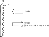
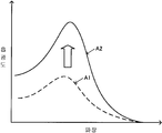
예컨대, 이러한 센서로서, 상술한 특허 문헌 1의 수법이 있다. 이 수법에서는, 도 1에 나타낸 바와 같이, 투명 기판(10)의 표면에 금속 미립자(20)를 고정하고, 이 투명 기판(10)에 대해 입사광을 조사하여, 금속 미립자(20)를 투과한 반사광의 흡광도를 측정한다. 도 2에 나타낸 바와 같이, 금속 미립자(20)에 표적물이 부착되어 있는 경우에는, A1로 나타내는 흡광도 스펙트럼으로부터 A2로 나타내는 흡광도 스펙트럼으로 변화된다. 특허 문헌 1의 수법에서는, 이 흡광도의 변화에 의해, 금속 미립자 근방의 매질의 변화를 검출하여, 표적물의 흡착이나 퇴적을 검출한다. For example, as such a sensor, there is a method of
그러나 이 수법에서는, 금속 미립자의 크기나 형상을 균일하게 제작하는 것이나, 금속 미립자를 규칙적으로 배열하는 것이 곤란하다. 금속 미립자의 크기나 배열을 제어할 수 없다면, 플라즈몬 공명으로 생기는 흡수나 공명 파장에도 편차가 생긴다. 이 때문에, 도 2에 나타낸 바와 같이, 흡광도 스펙트럼의 폭이 넓어져서, 피크 강도가 저하되어 버린다. 그리고, 피크 강도가 저하되면, 금속 미립자 근방의 매질의 변화를 검출하는 신호 변화가 작아져서, 센서 감도를 향상시키는데에도 한계가 생겨 버린다. 이 때문에, 흡광도 스펙트럼으로부터 물질을 특정하고자는 용도로는, 센서의 감도가 불충분하게 되어 버린다. However, in this method, it is difficult to uniformly produce the size and shape of the metal fine particles and to arrange the metal fine particles regularly. If the size and arrangement of the metal fine particles cannot be controlled, variations occur in the absorption and resonance wavelengths caused by plasmon resonance. For this reason, as shown in FIG. 2, the width | variety of the absorbance spectrum becomes wide and the peak intensity falls. When the peak intensity decreases, the signal change for detecting the change of the medium in the vicinity of the metal fine particles becomes small, and there is a limit in improving the sensor sensitivity. For this reason, the sensitivity of the sensor becomes insufficient for the purpose of specifying the substance from the absorbance spectrum.
그런데, 센서의 감도를 향상시키는 수법으로서, 상술한 센서를 표면 증강 라만 산란(SERS:Surface Enhanced Raman Scattering)에 적용하는 수법을 생각할 수 있다. 이 수법은, 표면 플라즈몬 공명에 의해서 라만 산란광을 증강시킴으로써, 라만 분광의 감도를 향상시키는 수법이다. By the way, as a method of improving the sensitivity of the sensor, a method of applying the above-described sensor to Surface Enhanced Raman Scattering (SERS) can be considered. This method is a method of improving the sensitivity of Raman spectroscopy by augmenting Raman scattered light by surface plasmon resonance.
그러나, 이 수법에서는, 여기 파장(도 4(a)에 나타내는 λ1)과 라만 산란 파장(λ2)에 있어서의 전장 증강도에 의해서 센서 감도가 결정되기 때문에(아래의 식 (1)), 양 파장에 있어서 전장 증강도를 향상시켜야 한다. However, in this technique, since the sensor sensitivity is determined by the electric field enhancement degree in the excitation wavelength (λ1 shown in Fig. 4A) and the Raman scattering wavelength λ2 (Equation (1) below), both wavelengths It is necessary to improve the electric field augmentation.
예컨대, 종래의 표면 증강 라만 산란 센서에서는, 공명 피크를 한 개만 이용하기 때문에, 공명 피크의 파장을 여기 파장 또는 라만 산란 파장 중 어느 하나에 맞춰야 한다. 이 경우, 어느 한쪽의 산란 과정에서의 전장 증강 효과만을 이용하게 되어서, 높은 전장 증강 효과는 기대할 수 없다. For example, in the conventional surface enhanced Raman scattering sensor, since only one resonance peak is used, the wavelength of the resonance peak must be adjusted to either the excitation wavelength or the Raman scattering wavelength. In this case, only the full-length enhancer effect in either scattering process is used, and a high full-field enhancer effect cannot be expected.
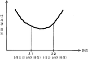
또한, 상술한 특허 문헌 1의 센서를 표면 증강 라만 산란에 적용했다고 가정한다. 이 경우, 도 2로 상술한 바와 같이, 넓은 표면 플라즈몬 공명 피크가 하나밖에 존재하지 않기 때문에, 여기 파장과 라만 산란 파장에 대해, 공명 피크의 위치를 적절한 위치로 설정할 필요가 있다. 즉, 이 공명 피크 파장이 국재 전장의 증강도에 큰 영향을 미치기 때문이다. 구체적으로는, 도 3에 나타낸 바와 같이, 라만 시프트에 대해서 비교적 넓은 공명 피크를 얻을 수 있다. 이 때문에, 공명 피크 파장을 여기 파장과 라만 산란 파장 사이로 설정하면, 여기 과정과 라만 산란 과정 양쪽에서 전장 증강 효과를 기대할 수 있다. 그러나 공명 피크가 넓기 때문에, 개개의 과정에서는 공명의 강도가 약해져서, 과정 전체의 증강도는 충분하다고할 수 없다. In addition, suppose that the sensor of
2. 본 실시예의 수법 2. Technique of this embodiment
그래서, 본 실시예에서는, 전기 전도체 격자의 일례인 금속 격자에 입사광을 비스듬히 입사시켜서 공명 피크를 2개 발생시키며, 이 2개의 공명 피크를 여기 파장과 라만 산란 파장에 설정함으로써 센서 감도를 향상시킨다. 이하에서는, 이 본 실시예의 수법에 대해서 설명한다. 우선, 본 실시예에 사용되는 라만 산란 분광법에 대해서 설명한다. Thus, in the present embodiment, two resonance peaks are generated by incidence of incident light on a metal grating, which is an example of an electrical conductor grating, and the two sensory resonance peaks are set to an excitation wavelength and a Raman scattering wavelength to improve sensor sensitivity. The method of this embodiment will be described below. First, the Raman scattering spectroscopy used for this Example is demonstrated.
도 4(a)에, 라만 산란 분광법의 원리적인 설명도를 나타낸다. 도 4(a)에 나타낸 바와 같이, 단일 파장의 광 Lin을 표적 분자 X(표적물)에 조사하면, 산란광 중에는, 입사광 Lin의 파장 λin과는 다른 파장 λ2의 라만 산란광 Ram이 발생한다. 이 라만 산란광 Ram과 입사광 Lin의 에너지 차이는, 표적 분자 X의 진동 준위나 회전 준위나 전자 준위의 에너지에 대응하고 있다. 표적 분자 X는, 그 구조에 따른 특유의 진동 에너지를 갖기 때문에, 단일 파장의 광 Lin을 이용함으로써 표적 분자 X를 특정할 수 있다. In Fig.4 (a), the principal explanatory drawing of Raman scattering spectroscopy is shown. As shown in Fig. 4 (a), when a single wavelength of light Lin is irradiated to the target molecule X (target), the scattered light generates Raman scattered light Ram having a wavelength? 2 different from the wavelength? In of the incident light Lin. The energy difference between the Raman scattered light Ram and the incident light Lin corresponds to the energy of the vibration level, rotation level, or electron level of the target molecule X. Since the target molecule X has a vibration energy peculiar to its structure, the target molecule X can be specified by using the light Lin of a single wavelength.
예컨대, 입사광 Lin의 진동 에너지를 V1라고 하고, 표적 분자 X의 진동 에너지를 V2라고 하며, 라만 산란광 Ram의 진동 에너지를 V3라고 하면, V3=V1-V2가 된다. 즉, V3가 V2에 따른 진동 에너지가 되기 때문에, 라만 산란광 Ram의 파장 λ2을 측정함으로써, 표적 분자 X를 특정할 수 있다. For example, if the vibration energy of the incident light Lin is V1, the vibration energy of the target molecule X is V2, and the vibration energy of the Raman scattered light Ram is V3, V3 = V1-V2. That is, since V3 becomes the vibration energy according to V2, the target molecule X can be specified by measuring the wavelength lambda 2 of the Raman scattered light Ram.
한편, 입사광 Lin의 대부분은 표적 분자 X에 충돌한 후에도 충돌 전과 같은 크기의 에너지를 갖고 있다. 이 탄성적인 산란광을 레일리-산란광 Ray라고 한다. 예컨대, 레일리-산란광 Ray의 진동 에너지를 V4라고 하면, V4=V1이다. 즉, 레일리-산란광 Ray의 파장 λ1은, λ1=λin이다. On the other hand, most of the incident light Lin has the same energy as before the impact even after impacting the target molecule X. This elastic scattered light is called Rayleigh-scattered light Ray. For example, when the vibration energy of Rayleigh-scattered light Ray is V4, V4 = V1. That is, the wavelength [lambda] 1 of Rayleigh-scattered light Ray is [lambda] 1 = (lambda) in.
도 4(b)에, 라만 산란 분광에 의해 취득되는 라만 스펙트럼(라만 시프트와 라만 산란 강도의 관계)의 예를 도시한다. 도 4(b)에 나타내는 그래프의 가로축은 라만 시프트를 나타낸다. 라만 시프트란, 라만 산란광 Ram의 파수(진동수)와 입사광 Lin의 파수의 차로, 표적 분자 X의 분자 결합 상태에 특유의 값을 취한다. In FIG.4 (b), the example of the Raman spectrum (Raman shift and Raman scattering intensity) acquired by Raman scattering spectroscopy is shown. The horizontal axis of the graph shown in FIG. 4B represents a Raman shift. Raman shift is a difference between the wave number (frequency) of the Raman scattered light Ram and the wave number of the incident light Lin, and takes a value peculiar to the molecular binding state of the target molecule X.
도 4(b)에 나타낸 바와 같이, B1로 나타내는 라만 산란광 Ram의 산란 강도(스펙트럼 피크)와, B2에 나타내는 레일리-산란광 Ray의 산란 강도를 비교하면, 라만 산란광 Ram 쪽이 미약하다는 것을 알 수 있다. 이와 같이, 라만 산란 분광법은 표적 분자 X의 식별 능력은 우수한 반면, 표적 분자 X를 센싱하는 감도 자체는 낮은 측정 수법이다. 이 때문에, 본 실시예에서는, 표면 증강 라만 산란에 의한 분광법을 이용해서, 센서의 고감도화를 도모하고 있다. As shown in Fig. 4B, when the scattering intensity (spectral peak) of the Raman scattered light Ram represented by B1 is compared with the scattered intensity of the Rayleigh-scattered light Ray shown in B2, it can be seen that the Raman scattered light Ram is weaker. . As such, Raman scattering spectroscopy is excellent in identifying the target molecule X, while the sensitivity itself of sensing the target molecule X is low. For this reason, in the present Example, the sensor is made highly sensitive using the spectroscopy by surface enhancement Raman scattering.
이 표면 증강 라만 산란을 응용한 고감도인 표면 플라즈몬 공명 센서를 실현하기 위해서는, 국소 전장의 증강도(이하, 적절히 줄여서 증강도라고 한다)가 가능한 한 큰 것이 바람직하다. 증강도 α는, 아래의 식 (1)로 표시된다(M.Inoue, K.Ohtaka, J.Phys.Soc.Jpn., 52,3853(1983)). 여기서, α ray는, 여기 파장(레일리-산란 파장과 같다)에 있어서의 증강도이고, α ram은 라만 산란 파장에 있어서의 증강도이다. In order to realize a highly sensitive surface plasmon resonance sensor using this surface enhancement Raman scattering, it is preferable that the enhancement of the local electric field (hereinafter, referred to as an enhancement) is as large as possible. The degree of enhancement α is represented by the following formula (1) (M. Inoue, K. Ohtaka, J. Phys. Soc. Jpn., 52, 3853 (1983)). Here, alpha ray is the degree of enhancement at the excitation wavelength (the same as the Rayleigh scattering wavelength), and α ram is the degree of enhancement at the Raman scattering wavelength.
α=α ray×α ram (1) α = α ray × α ram (1)
위의 식 (1)로부터, 표면 증강 라만 산란 과정에서의 증강도를 높이기 위해서는, 여기 과정에 있어서의 증강도와 라만 산란 과정에서의 증강도 양쪽을 동시에 높일 필요가 있다. 이 때문에 본 실시예에서는, 도 5에 나타낸 바와 같이 여기 파장 및 라만 산란 파장의 근방에서만 강한 2개의 공명 피크를 발생시킨다. 이로써, 양 산란 과정의 상승 효과에 의해서, 국소 전장의 증강 효과를 비약적으로 높일 수 있다. From the above equation (1), in order to increase the degree of enhancement in the surface enhanced Raman scattering process, it is necessary to simultaneously increase both the degree of enhancement in the excitation process and the degree of enhancement in the Raman scattering process. For this reason, in the present embodiment, as shown in Fig. 5, two resonance peaks are generated that are strong only near the excitation wavelength and the Raman scattering wavelength. Thereby, the synergistic effect of both scattering processes can dramatically increase the enhancement effect of the local electric field.
3. 구성예 3. Configuration Example
도 6~도 9를 이용해서, 여기 파장과 라만 산란 파장 근방에 2개의 공명 피크를 발생시키는 본 실시예의 구성예에 대해서 설명한다. 한편, 이하에서는, 각 구성 요소를 도면 상에서 인식할 수 있을 정도의 크기로 하기 위해서, 각 구성 요소의 치수나 비율을 실제의 것과는 적당히 다르게 하고 있다. 6-9, the structural example of this Example which generate | occur | produces two resonance peaks in the vicinity of an excitation wavelength and a Raman scattering wavelength is demonstrated. In addition, in the following, in order to make each component into the magnitude | size which can be recognized on drawing, the dimension and ratio of each component are changed suitably from an actual thing.
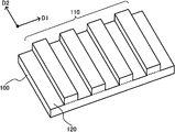
도 6은 본 실시예의 센서 칩(광 디바이스, 전기 전도체 격자)의 구성예의 사시도이다. 이 센서 칩은, 표면 플라즈몬 공명과 표면 증강 라만 산란을 이용해서 표적물(표적 물질, 표적 분자)를 검출하기 위한 것으로, 기재(100)(기판), 제 1 돌기군(110)을 포함한다. 이 센서 칩은, 1차원의 주기성을 갖는 금속 격자이다. 6 is a perspective view of a configuration example of a sensor chip (optical device, electric conductor grating) of the present embodiment. This sensor chip detects a target (target substance, target molecule) using surface plasmon resonance and surface enhanced Raman scattering, and includes a substrate 100 (substrate) and a
또한 이하에서는, 센서 칩이, 금속으로 형성되는 금속 격자인 경우를 예로 설명하지만, 본 실시예에서는 이 경우로 한정되지 않는다. 즉, 센서 칩은, 전기 전도체에 의해 형성되는 격자이면 되고, 예컨대 반도체(예컨대, 폴리 실리콘)에 의해 형성되는 격자여도 된다. In the following, the case where the sensor chip is a metal grating formed of metal is described as an example, but the present embodiment is not limited to this case. In other words, the sensor chip may be a lattice formed of an electrical conductor or may be, for example, a lattice formed of a semiconductor (for example, polysilicon).
구체적으로는, 기재(100)는 Ag(은)이나 Au(금) 등의 금속(넓은 의미로는 전기 전도체)을 포함하며, 예컨대 사각형이나 원형의 평판 형상으로 형성된다. 제 1 돌기군(110)은 기재(100)의 평면(넓은 의미로는 면)에 따른 제 1 방향(D1)으로 주기적으로 배치되고, 예컨대 기재(100)와 같은 금속에 의해 형성된다. 여기서, 기재(100)의 평면은, 예컨대 제 1 돌기군(110)이 형성되는 쪽의 기재(100)의 표면(120)이다. Specifically, the
보다 구체적으로는, 제 1 돌기군(110)의 각 돌기는, 돌기의 배열 방향(D1)의 단면 형상이 기재(100)의 표면(120)으로부터 볼록 형상으로 형성된다. 볼록 형상은, 직사각형이나 사다리꼴, 원호 등이다. 예컨대, 도 6에 나타낸 바와 같이, 제 1 돌기군(110)은, 기재(100)를 바라본 평면도에 있어서, 방향(D1)에 직교하는 제 2 방향(D2)에 평행한 줄무늬 형상으로 형성된다. More specifically, each protrusion of the
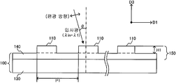
도 7에, 본 실시예의 센서 칩의 단면도를 나타낸다. 이 단면도의 단면은, 기재(100)의 평면에 수직인 면이며, 제 1 돌기군(110)의 배열 방향(D1)에 평행한 면이다. 도 7에 나타낸 바와 같이, 기재(100)의 평면의 법선 방향을 방향(D3)라고 한다. 7 is a sectional view of the sensor chip of this embodiment. The cross section of this cross section is a surface perpendicular | vertical to the plane of the
기재(100)는 유리 기판(130) 위에 금속 박막(140)을 형성한 것이다. 예컨대, 금속 박막(140)의 두께는 150nm이상이다. 제 1 돌기군(110)의 단면 형상은 직사각형(대략 직사각형)이며, 높이(H1)인 돌기가, 방향(D1)을 따라 제 1 주기(P1)로 배열된다. 이 금속 박막(140)과 제 1 돌기군(110)에 의해 금속 격자(150)(주기적인 금속 요철 구조)가 형성된다. 주기(P1)는 100~1000nm의 범위로 설정되고, 높이(H1)는 10~100nm의 범위로 설정되는 것이 바람직하다. The
이 센서 칩에는 직선 편광을 포함하는 입사광이 입사된다. 직선 편광의 편광 방향(편광 방향)은, 방향(D1)과 방향(D3)에 평행한 면에 대해 평행한 방향이다. 이 입사광은, 금속 박막(140)과 제 1 돌기군(110)에 의한 금속 격자(150)에 대해 경사시켜서 입사시킨다. 구체적으로는, 경사각을 θ이라고 하면, θ>0이며, 도 7에 나타내는 단면에 있어서 입사 방향과 방향(D3)의 반대 방향과의 각도(기재(100)의 평면을 향하는 수직선에 대한 각도)가 θ가 되도록 입사광을 입사시킨다. Incident light including linearly polarized light is incident on the sensor chip. The polarization direction (polarization direction) of linearly polarized light is a direction parallel to the surface parallel to direction D1 and the direction D3. This incident light is made to incline with respect to the
또한 상기에서는, 직선 편광이 방향(D1)과 방향(D3)에 평행한 면에 대해 평행이라고 했지만, 본 실시예에서는, 직선 편광이 상기한 면에 대해 비평행이어도 되고, 상기 면에 평행한 편광 성분을 포함하고 있으면 된다. 또한, 상기에서는, 기재(100)로서 유리 기판(130) 위에 금속 박막(140)을 형성한 것을 이용하고 있지만, 본 실시예는 이것에 한정되지 않는다. 예컨대, 본 실시예의 기재(100)는, 석영 기판이나 사파이어 기판 위에 금속막을 형성한 것이어도 된다. 또한, 기재(100)로서 금속으로 이루어지는 평판을 이용해도 된다. In addition, in the above, although linearly polarized light was said to be parallel with respect to the surface parallel to direction D1 and the direction D3, in this Example, linearly polarized light may be non-parallel with respect to the said surface, and is polarized parallel to the said surface. What is necessary is just to contain a component. In addition, in the above, although the metal
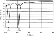
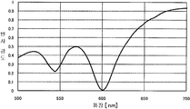
도 8에, 센서 칩의 반사광 강도의 특성예를 도시한다. 도 8은, 금속 격자를 Ag에 의해 형성하고, 금속 격자에 대한 광의 입사 각도θ가 3도이며, 광의 편광 방향이 금속 격자의 홈 방향(D2)과 직교하고, 돌기의 단면이 직사각형(대략 직사각형)이며, 주기(P1)가 500nm이고, 높이(H1)가 20nm인 경우의 특성예이다. 한편, 가로축은 반사광의 파장을 나타내고, 세로축은 반사광 강도(입사광 강도에 대한 비율)를 나타낸다. 8, the characteristic example of the reflected light intensity of a sensor chip is shown. 8 shows that the metal lattice is formed of Ag, the incident angle θ of light to the metal lattice is 3 degrees, the polarization direction of the light is orthogonal to the groove direction D2 of the metal lattice, and the cross section of the projection is rectangular (approximately rectangular). Is a characteristic example when the period P1 is 500 nm and the height H1 is 20 nm. On the other hand, the horizontal axis represents the wavelength of the reflected light, and the vertical axis represents the reflected light intensity (ratio to incident light intensity).
도 8에 나타낸 바와 같이, 본 실시예의 금속 격자에는, 표면 플라즈몬 폴라리톤(SPP:Surface Plasmon Polariton)의 공명 피크가 2개 존재한다. 예컨대, 하나의 공명 피크는 파장 515nm 부근에 위치하고, 다른 하나의 공명 피크는 파장 555nm 부근에 위치한다. 이 2개의 공명 피크를, 여기 파장과 라만 산란 파장의 근방에 맞춤으로써(또는 일치시킴으로써), 큰 증강 라만 산란 효과를 기대할 수 있다. 예컨대, 파장 515nm의 아르곤 레이저를 여기 파장으로서 이용한 경우, 파장 555nm 근방의 라만 산란광(라만 시프트 1200~1600cm-1)을 강하게 증강시키는 것이 가능해진다. As shown in Fig. 8, two resonance peaks of the surface plasmon polariton (SPP) exist in the metal lattice of the present embodiment. For example, one resonance peak is located near wavelength 515 nm and the other resonance peak is located near wavelength 555 nm. By fitting (or matching) these two resonance peaks to the vicinity of the excitation wavelength and the Raman scattering wavelength, a large enhancement Raman scattering effect can be expected. For example, it is possible to the case of using an argon laser with a wavelength of 515nm as an excitation wavelength, and a strong Raman scattering light (
한편, 본 실시예가 적용되는 표적물로서, 예컨대 마약이나 알코올이나 잔류 농약 등의 희박한 분자나, 바이러스 등의 병원체를 상정할 수 있다. On the other hand, as a target to which the present embodiment is applied, for example, lean molecules such as drugs, alcohols or residual pesticides, and pathogens such as viruses can be assumed.
4. 공명 피크 파장의 설정 수법 4. Setting method of resonance peak wavelength
도 9를 이용해서, 2개의 공명 피크 파장의 설정 수법에 대해서 설명한다. 우선, 본 실시예의 센서 칩의 기능에 대해서 설명한다. 9, the method of setting two resonance peak wavelengths is demonstrated. First, the function of the sensor chip of the present embodiment will be described.
센서 칩의 격자면에 광이 입사하면, 격자의 요철에 의해 표면 플라즈몬이 발생한다. 본 실시예에서는, 센서 칩의 격자면에 대해 비스듬하게 광을 입사시킨다. 이 입사각 θ는 수 도(예컨대 10도 이하)이다. 입사광의 편광 방향을 격자의 홈 방향과 직교시켜 두면, 금속 격자 내의 자유 전자의 진동에 동반해서 전자파의 진동이 여기된다. 이 전자파의 진동은 자유 전자의 진동에 영향을 미치기 때문에, 양자의 진동이 결합된 계(system)인 표면 플라즈몬 폴라리톤이 형성된다. When light enters the grating plane of the sensor chip, surface plasmons are generated by the irregularities of the grating. In this embodiment, light is incident at an angle to the grating plane of the sensor chip. This incident angle θ is several degrees (for example, 10 degrees or less). When the polarization direction of the incident light is orthogonal to the groove direction of the grating, vibration of the electromagnetic wave is excited along with vibration of free electrons in the metal grating. Since the vibration of the electromagnetic wave affects the vibration of the free electrons, a surface plasmon polaritone, a system in which both vibrations are combined, is formed.
이 표면 플라즈몬 폴라리톤은, 센서 칩의 표면을 따라 전파한다. 구체적으로는, 표면 플라즈몬 폴라리톤은, 공기와 금속 격자와의 계면을 따라 전파해서, 금속 격자의 근방에 강한 국소 전장을 여기한다. 표면 플라즈몬 폴라리톤의 결합은 광의 파장에 대해서 민감하며, 그 결합 효율은 높다. 그리고, 격자 표면에 예컨대 1~수개의 표적물이 흡착하면, 여기에서 표면 증강 라만 산란이 발생한다. 이와 같이, 공기 전파 모드인 입사광으로부터 표면 플라즈몬 폴라리톤을 통해서 증강 전장을 여기하고, 증강 전장과 표적물의 상호 작용에 의해 표면 증강 라만 산란을 발현시킨다. 본 실시예에서는, 반사광 강도 스펙트럼의 폭이 좁아서, 2개의 공명 피크를 날카롭게 할 수 있다. 이로써, 센서 감도의 향상을 도모하여, 표면 증강 라만 산란 스펙트럼으로부터 표적 물질을 특정하는 것이 가능한 센서 칩을 실현할 수 있다. This surface plasmon polaritone propagates along the surface of the sensor chip. Specifically, the surface plasmon polaritone propagates along the interface between air and the metal lattice, and excites a strong local electric field in the vicinity of the metal lattice. The binding of surface plasmon polaritone is sensitive to the wavelength of light, and its coupling efficiency is high. And when one or several targets adsorb | suck to a grating surface, for example, surface enhancement Raman scattering arises here. As such, the enhanced electric field is excited through the surface plasmon polaritone from the incident light in the air propagation mode, and the surface enhanced Raman scattering is expressed by the interaction of the enhanced electric field with the target. In this embodiment, the width of the reflected light intensity spectrum is narrow, so that two resonance peaks can be sharpened. Thereby, the sensor chip which can aim at the improvement of a sensor sensitivity and can specify a target substance from the surface enhancement Raman scattering spectrum can be realized.
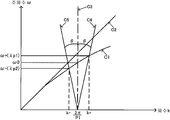
도 9에, 표면 플라즈몬 폴라리톤의 여기 조건의 설명도를 나타낸다. 도 9에 나타내는 C1은 표면 플라즈몬 폴라리톤의 분산 곡선(예컨대, 공기와 Au의 경계면에서의 분산 곡선)을 나타내고, C2는 라이트 라인(a light line)을 나타낸다. 도 9에서는, 금속 격자의 주기를 P1으로 하고, 이 경우의 격자 벡터의 파수 2π/P1를 가로축 상에 나타낸다. Explanatory drawing of the excitation condition of surface plasmon polaritone is shown in FIG. C1 shown in FIG. 9 shows the dispersion curve of surface plasmon polaritone (for example, the dispersion curve in the interface of air and Au), and C2 shows a light line. In Fig. 9, the period of the metal lattice is set to P1, and the wave number 2π / P1 of the lattice vector in this case is shown on the horizontal axis.
우선, 금속 격자와 여기 조건의 관계에 대해서 설명한다. 입사광의 파수를 ki라고 하고, 입사 각도를 θ라고 하면, 금속 격자의 배열 방향(도 7에 나타내는 방향 D1, 또는 -D1)에 있어서의 1차 에버네슨트(evanescent)파의 파수는, 2π/P1± ki·sinθ이다. 표면 플라즈몬 폴라리톤은, 이 에버네슨트파의 파수 2π/P1± ki·sinθ와 표면 플라즈몬의 파수가 일치한 경우에 여기된다. 즉, 표면 플라즈몬 폴라리톤의 여기 조건은, 에버네슨트파의 생성 조건을 나타내는 직선과 표면 플라즈몬 폴라리톤의 분산 곡선과의 교점에 의해 표시된다. First, the relationship between a metal lattice and an excitation condition is demonstrated. If the wave number of incident light is ki and the angle of incidence is θ, the wavenumber of the primary evanescent wave in the arrangement direction of the metal lattice (direction D1 or -D1 shown in FIG. 7) is 2π /
도 9의 C3에, 본 실시예의 비교예로서 금속 격자에 대해 수직(θ=0)으로 광을 입사시킨 경우의 에버네슨트파의 생성 조건을 나타내는 직선을 나타낸다. C3에 나타낸 바와 같이, 이 경우의 에버네슨트파의 파수는 2π/P1으로 표시된다. 이 직선 C3은, 격자 벡터의 파수의 위치로부터 위로 연장시킨 선으로, 표면 플라즈몬 폴라리톤의 분산 곡선 C1과 교차된다. 이 때, 교점은 하나로, 공명 피크는 주파수 ω0(각(角) 주파수) 하나만 나타난다. In Fig. 9 C3, a straight line showing the conditions for generating an Evernesent wave when light is incident perpendicularly to the metal lattice (θ = 0) as a comparative example of the present embodiment is shown. As shown in C3, the wavenumber of the Evernesent wave in this case is represented by 2π / P1. This straight line C3 is a line extending upward from the position of the wavenumber of the lattice vector and intersects with the dispersion curve C1 of the surface plasmon polaritone. At this time, there is only one intersection point, and only one resonance peak appears at a frequency ω 0 (each frequency).
C4과 C5에, 본 실시예에서의 에버네슨트파의 생성 조건을 나타내는 직선을 나타낸다. 본 실시예와 같이 금속 격자에 대하여 각도 θ(θ>0)로 광을 입사시킨 경우, 에버네슨트파의 파수는 2π/P1±ki·sinθ으로 표시된다. 직선 C4은 2π/P1+ki·sinθ에 대응하고, 직선 C5은, 2π/P1-ki·sinθ에 대응한다. 이들 직선 C4과 C5는 격자 벡터의 파수의 위치로부터 각도θ로 기울여서 위로 연장시킨 선으로, 표면 플라즈몬 폴라리톤의 분산 곡선 C1과 2점에서 교차한다. 따라서, 공명 피크는 주파수 ω+와 ω-의 2개(각각 파장 λp1과 λp2에 대응한다)가 나타난다. In C4 and C5, the straight line which shows the generation conditions of the evernesent wave in a present Example is shown. In the case where light is incident on the metal lattice at an angle θ (θ> 0) as in the present embodiment, the wavenumber of the Evernet wave is represented by 2π / P1 ± ki · sinθ. The straight line C4 corresponds to 2π / P1 + kisinθ, and the straight line C5 corresponds to 2π / P1-kisinθ. These straight lines C4 and C5 are lines extending upward by tilting at an angle θ from the position of the wave vector of the lattice vector, and intersect at two points with the dispersion curve C1 of the surface plasmon polaritone. Therefore, two resonance peaks (corresponding to the wavelengths λp1 and λp2, respectively) of the frequencies ω + and ω- appear.
본 실시예에서는, 상기한 표면 플라즈몬 폴라리톤의 여기 조건을 이용해서 2개의 공명 피크 파장 λp1과 λp2를 설정하고, 이 2개의 공명 피크 파장을 표면 증강 라만 산란에 이용한다. 구체적으로는, 우선 엄밀 결합파 해석(RCWA:Rigorous Coupled Wave Analysis)에 의해 분산 곡선 C1을 구한다(L. Li and C. W. Haggans, J. Opt. Soc. Am., A10, 1184-1189(1993)). 분산 곡선 C1은, 금속의 종류나, 매질의 종류나, 금속 격자의 단면 형상에 고유의 곡선이다. 다음으로 원하는 격자 주기(P1)와 입사 각도(θ)를, 표적물의 라만 시프트에 따라서 결정한다. 즉, 제 1 공명 피크 파장 λp1을 여기 파장(레일리-산란 파장) 근방으로 설정하고, 제 2 공명 피크 파장 λp2(λp2>λp1)을 라만 산란 파장의 근방으로 설정한다. 그리고, 분산 곡선 C1과 ω=ω+(λ=λp1)의 교점을 직선 C4가 지나고, 분산 곡선 C1과 ω=ω-(λ=λp2)의 교점을 직선 C5가 지나도록, 격자 주기(P1)와 입사 각도(θ)를 설정한다. In this embodiment, two resonance peak wavelengths λp1 and λp2 are set using the above-described excitation conditions of the surface plasmon polaritone, and the two resonance peak wavelengths are used for surface enhanced Raman scattering. Specifically, first, a dispersion curve C1 is obtained by a rigid coupled wave analysis (RCWA) (L. Li and CW Haggans, J. Opt. Soc. Am., A10, 1184-1189 (1993)). . Dispersion curve C1 is a curve inherent in the kind of metal, the kind of medium, and the cross-sectional shape of a metal lattice. Next, the desired lattice period P1 and the incident angle θ are determined in accordance with the Raman shift of the target. That is, the first resonance peak wavelength λp1 is set near the excitation wavelength (Rayley-scattering wavelength), and the second resonance peak wavelength λp2 (λp2> λp1) is set near the Raman scattering wavelength. The lattice period P1 is such that the straight line C4 passes through the intersection point of the dispersion curve C1 and ω = ω + (λ = λp1) and the straight line C5 passes through the intersection point of the dispersion curve C1 and ω = ω− (λ = λp2). And the angle of incidence θ are set.
이렇게 해서, 금속 격자의 소재나, 형상, 높이(H1), 격자 주기(P1), 광의 입사 각도(θ)를 설정함으로써, 2개의 공명 피크의 파장 λp1과 λp2를 원하는 값으로 설정할 수 있다. In this way, the wavelengths? P1 and? P2 of the two resonance peaks can be set to desired values by setting the material of the metal lattice, the shape, the height H1, the lattice period P1, and the incident angle? Of the light.
그런데, 비교예로 상술한 바와 같이, 표면 플라즈몬 공명이 하나의 넓은 공명 피크밖에 갖지 않는 경우, 표면 증강 라만 산란의 과정 전체에서 충분한 전장 증강 효과를 얻기 어렵다는 과제가 있다. However, as described above in the comparative example, when the surface plasmon resonance has only one wide resonance peak, there is a problem that it is difficult to obtain a sufficient electric field enhancement effect throughout the entire surface enhancement Raman scattering process.
이 점, 본 실시예의 광 디바이스는, 도 7에 나타낸 바와 같이, 전기 전도체의 돌기를, 기재(100)의 평면(넓은 의미로는 가상 평면)에 대해 평행한 방향(D1)을 따라 제 1 주기(P1)(P1<λ1)로 배열한 제 1 돌기군(110)을 갖는다. 이 제 1 주기(P1)로 배열된 제 1 돌기군(110)에는, 기재(100)의 평면을 향하는 수직선에 대해 경사진 방향으로 진행하는 광(파장 λ1, 입사 각도θ)이 입사된다. 이 입사광에 의해, 도 9에 나타낸 바와 같이, 제 1 공명 피크 파장 λp1과 제 2 공명 피크 파장 λp2 각각으로 표면 플라즈몬 공명이 발생한다. 이 때, 도 8에 나타낸 바와 같이, 제 1 공명 피크 파장 λp1을 포함하는 제 1 공명 피크 파장 대역 BW1은, 표면 증강 라만 산란에 있어서의 여기 파장 λ1을 포함한다. 제 2 공명 피크 파장 λp2을 포함하는 제 2 공명 피크 파장 대역 BW2은, 표면 증강 라만 산란에 있어서의 라만 산란 파장 λ2을 포함한다. In this regard, in the optical device of the present embodiment, as shown in FIG. 7, the projection of the electrical conductor has a first period along the direction D1 parallel to the plane (in a broad sense, the virtual plane) of the
여기서, 대역 BW1, BW2의 폭이란, 소정의 반사광 강도에서의 대역폭으로, 예컨대 피크의 반값폭이다. 한편, 도 8에서는 λ1=λp1, λ2=λp2로 하고 있지만, 본 실시예에서는 λ1과 λp1는 달라도 되고, λ2과 λp2는 달라도 된다. 또한, 가상 평면이란, 제 1 돌기군(110)의 배열 방향이나 입사광의 입사 각도 등의 기준이 되는 평면으로, 예컨대 기재(100)의 평면(예컨대 기재(100)의 표면(120))에 평행한 면이다. Here, the widths of the bands BW1 and BW2 are bandwidths at predetermined reflected light intensities, for example, half-widths of peaks. In FIG. 8,
상기 실시예에 의하면, 표면 증강 라만 산란의 과정 전체에서 전장 증강도를 향상시키는 것이 가능하게 된다. 즉, 2개의 공명 피크 파장 대역 BW1, BW2이 파장λ1, λ2을 포함하도록 주기(P1)나 입사 각도(θ) 등이 설정됨으로써 여기 파장 λ1에 있어서의 전장 증강도와 라만 산란 파장 λ2에 있어서의 전장 증강도를 향상시킬 수 있다. According to the above embodiment, it is possible to improve the electric field enhancement degree throughout the entire process of surface enhancement Raman scattering. That is, the period P1, the incidence angle θ, and the like are set such that the two resonance peak wavelength bands BW1 and BW2 include the wavelengths λ1 and λ2, so that the electric field enhancement at the excitation wavelength λ1 and the electric field at the Raman scattering wavelength λ2 are achieved. It can improve the degree of reinforcement.
또한, 상기 실시예에 의하면, 금속 격자의 소재나, 단면 형상, 주기(P1), 높이(H1), 광의 입사 각도(θ)를 적절하게 변경함으로써, 2개의 공명 피크의 위치와 간격을 임의의 값으로 맞출 수 있다. 이 때문에, 표적물을 특정할 때에 조사하는 광의 파장 λin을 적절하게 선택하는 것이 가능해져서, 측정 파장 범위의 폭을 넓힐 수 있다. Further, according to the above embodiment, the position and spacing of the two resonance peaks can be arbitrarily changed by suitably changing the material of the metal lattice, the cross-sectional shape, the period P1, the height H1, and the incident angle θ of light. Can be set to a value. For this reason, when specifying a target, the wavelength (lambda) in of the light to irradiate can be selected suitably, and the width | variety of a measurement wavelength range can be expanded.
또한, 본 실시예에서는, 라만 산란 파장 λ2은 여기 파장 λ1보다 긴 파장(λ2>λ1)이다. In addition, in this embodiment, the Raman scattering wavelength λ 2 is a wavelength (λ 2> λ 1) longer than the
이와 같이 하면, 라만 산란광의 스토크스 성분과 반스토크스 성분 중, 산란 강도가 보다 큰 스토크스 성분을 측정할 수 있다. 한편, 본 실시예에서는, λ2<λ1인 반스토크스 성분을 이용해도 된다. By doing in this way, the Stokes component with larger scattering intensity | strength can be measured among the Stokes component and anti-stalk component of Raman scattered light. In addition, in this embodiment, you may use the anti-stokes component of (lambda) 2 <(lambda) 1.
또한, 본 실시예에서는, 도 7에 나타낸 바와 같이, 입사광으로서, 편광 방향의 기재(100)의 평면에 평행한 성분(편광 방향의 기재(100)의 평면에 대한 정사영)과 제 1 돌기군(110)의 배열 방향(D1)이 평행한 직선 편광이 입사된다. In addition, in the present embodiment, as shown in FIG. 7, as incident light, a component parallel to the plane of the
이와 같이 하면, 직선 편광에 의해서 자유 전자 플라즈마의 조밀파가 방향(D1)에 따른 방향으로 유기되어, 제 1 돌기군(110)의 배열 방향(D1)을 따라 전파하는 표면 플라즈몬를 여기할 수 있다. In this way, the surface plasmons propagating along the alignment direction D1 of the
또한, 본 실시예에서는, 도 12 등으로 후술하는 바와 같이, 제 1 돌기군(110)의 정상면(220)에, 금속에 의해 형성되는 제 2 돌기군(200)을 포함해도 된다. 그리고, 제 2 돌기군(200)은, 기재(100)의 평면에 평행한 방향(D1)을 따라서, 제 1 주기(P1)보다 짧은 제 2 주기(P2)(P2<P1)로 배열되어도 된다. In addition, in the present embodiment, as described later in FIG. 12 or the like, the
또한, 본 실시예에서는, 도 12 등으로 후술하는 바와 같이, 제 1 돌기군(110)이 배열된 면이며, 제 1 돌기군(110)의 이울하는 돌기 사이의 면(230)(제 1 돌기군(110)의 이웃하는 돌기 사이의 바닥면(230))에, 금속에 의해 형성되는 제 3 돌기군(210)을 포함해도 된다. 그리고, 제 3 돌기군(210)은, 기재(100)의 평면에 평행한 방향(D1)을 따라서, 상기 제 1 주기(P1)보다 짧은 제 3 주기(P3)(P3<P1)로 배열되어도 된다. In addition, in the present embodiment, as will be described later with reference to FIG. 12 and the like, the
이와 같이 하면, 제 1 돌기군(110)에 의해 전파형의 표면 플라즈몬이 여기되고, 이 전파형의 표면 플라즈몬에 의해 제 2 돌기군(200)이나 제 3 돌기군(210)에 국재형의 표면 플라즈몬이 여기된다. 이로써, 여기 파장과 라만 산란 파장에 있어서의 전장 증강도를 더 향상시킬 수 있다. In this way, the surface plasmon of the propagation type is excited by the
5. 변형예 5. Modifications
상술한 도 8에서는, 금속 격자(150)가 Ag에 의해 형성되는 경우에 대해서 설명했지만, 본 실시예에서는 금속 격자(150)가 Au에 의해 형성되어도 된다. 도 10에, 이 경우의 센서 칩의 반사광 강도의 특성예를 나타낸다. 도 10은 금속 격자에 대한 광의 입사 각도(θ)가 5도이고, 광의 편광 방향이 금속 격자의 홈과 직교하며, 돌기의 단면이 직사각형(대략 직사각형)이고, 주기(P1)가 500nm이며, 높이(H1)가 40nm인 경우의 특성예이다. In FIG. 8 described above, the case where the
도 10에 나타낸 바와 같이, 2개의 공명 피크 중 하나는 파장 545nm에 위치하고, 다른 하나는 파장 600nm에 위치하고 있다. 이 2개의 공명 피크를 여기 파장 및 라만 산란 파장의 근방에 맞춤으로써, 강한 표면 증강 라만 산란의 신호를 취득하는 것이 가능하게 된다. As shown in FIG. 10, one of the two resonance peaks is located at wavelength 545 nm and the other is located at
이 Au에 의해 형성된 금속 격자에서는, 도 8에 나타내는 Ag에 의해 형성된 금속 격자와 비교해서, 2개의 공명 피크의 파장이 다르고, 공명 피크가 약간 넓으며, 공명 피크가 낮게 되어 있다. 그러나 공명 피크를 하나 밖에 이용하지 않는 경우에 비해서, 표면 증강 라만 산란의 신호를 증강시키는 효과는 현저하게 우수하다. 또한, Au를 이용함으로써, 산화나 황화 등에 의한 표면 열화를 억지할 수 있다. 한편, 도 8에 나타낸 바와 같이, Ag를 이용한 경우에는, Au에 비해서 공명 피크가 좁고 깊다. 이 때문에, Au에 비해서, 표면 증강 라만 산란의 신호의 증강 효과를 보다 향상시킬 수 있다. In the metal lattice formed of Au, the wavelengths of the two resonance peaks are different, the resonance peaks are slightly wider, and the resonance peaks are lower than the metal lattice formed of Ag shown in FIG. 8. However, compared with the case where only one resonance peak is used, the effect of enhancing the signal of surface enhanced Raman scattering is remarkably excellent. Moreover, by using Au, surface deterioration by oxidation, sulfidation, etc. can be suppressed. On the other hand, as shown in Fig. 8, when Ag is used, the resonance peak is narrower and deeper than Au. For this reason, compared with Au, the augmentation effect of the signal of surface enhancement Raman scattering can be improved more.
여기서, 이상의 실시예에서는, 표면 플라즈몬이나, 표면 플라즈몬 폴라리톤, 표면 증강 라만 산란을 강하게 발현시키는 물성을 갖는 Ag나 Au를 이용했지만, 본 실시예에서는, 그 외에 Pt(백금)이나 Cu(구리), Al(알루미늄) 등의 금속을 이용해도 된다. Here, in the above embodiment, Ag or Au having physical properties that strongly express surface plasmon, surface plasmon polaritone, and surface enhanced Raman scattering was used. However, in the present embodiment, Pt (platinum) and Cu (copper) are used. And metals such as Al (aluminum) may be used.
6. 제 2 구성예 6. Second Configuration Example
상기 실시예에서는, 제 1 돌기군(110)에 의해 전파형의 표면 플라즈몬이 여기되었지만, 본 실시예에서는, 회절 격자가, 국재형의 표면 플라즈몬을 여기하는 다른 돌기군(금속 미세 구조)을 포함해도 된다. 도 11, 도 12를 이용해서, 이러한 센서 칩의 제 2 구성예에 대해서 설명한다. In the above embodiment, the propagation type surface plasmon is excited by the
도 11은 센서 칩의 제 2 구성예의 사시도이다. 이 센서 칩은, 기재(100), 제 1 돌기군(110), 제 2 돌기군(200), 제 3 돌기군(210)을 포함한다. 또한, 이하에서는, 도 7 등으로 설명한 구성 요소와 동일한 구성 요소에는 같은 부호를 붙이고, 적절하게 설명을 생략한다. 11 is a perspective view of a second configuration example of the sensor chip. This sensor chip contains the
도 11에 나타낸 바와 같이, 제 1 돌기군(110)은 기재(100)의 평면에 평행한 제 1 방향(D1)을 따라 주기적으로 배치된다. 그리고, 제 2 돌기군(200)은 제 1 돌기군(110)의 정상면(220)에, 방향(D1)을 따라서 주기적으로 배치된다. 제 3 돌기군(210)은 제 1 돌기군(110)의 돌기 사이의 바닥면(230)(기재(100)의 평면)에 방향(D1)을 따라서 주기적으로 배치된다. As shown in FIG. 11, the
보다 구체적으로는, 제 2 돌기군(200)과 제 3 돌기군(210)의 각 돌기는, 돌기의 배열 방향(D1)의 단면 형상이 정상면(220)과 바닥면(230)에 의해 볼록 형상으로 형성된다. 볼록 형상은, 직사각형이나 사다리꼴, 원호 등이다. 예컨대, 도 11에 나타낸 바와 같이, 제 2 돌기군(200)이나 제 3 돌기군(210)은, 기재(100)를 바라본 평면도 상에서, 방향(D2)에 평행한 줄무늬 형상으로 형성된다. 이 제 2 돌기군(200)과 제 3 돌기군(210)은, 제 1 돌기군(110)과 같은 금속에 의해 형성되어도 되고, 다른 금속에 의해 형성되어도 된다. More specifically, each projection of the
도 12에, 제 2 구성예의 센서 칩의 단면도를 나타낸다. 이 단면도의 단면은, 기재(100)의 평면에 수직인 면이며, 방향(D1)에 평행한 면이다. 도 12에 나타낸 바와 같이, 제 2 돌기군(200)은 정상면(220)으로부터의 높이가 H2이며, P1보다 짧은 주기(P2)로 배열된다. 제 3 돌기군(210)은 저면(230)으로부터의 높이가 H3이며, P1보다 짧은 주기(P3)로 배열된다. 예컨대, 주기(P2나 P3)는, 500nm 이하로 설정하는 것이 바람직하고, 높이(H2나 H3)는, 200nm 이하로 설정하는 것이 바람직하다. 한편, 높이(H3)는 H3>H1이어도 되고, H3≤H1이어도 된다. 12, sectional drawing of the sensor chip of a 2nd structural example is shown. The cross section of this cross section is a surface perpendicular | vertical to the plane of the
여기서, 상기에서는, 제 2 돌기군(200)이나 제 3 돌기군(210)의 배열 방향이, 제 1 돌기군(110)과 같은 배열 방향(D1)이라고 했지만, 본 실시예에서는 제 2 돌기군(200)이나 제 3 돌기군(210)의 배열 방향이 D1와 다른 방향이어도 된다. 이 경우, 배열 주기(P2나 P3)는, 방향(D1)에 있어서의 배열 주기가 된다. Here, in the above, although the arrangement direction of the
다음으로, 이 제 2 구성예의 센서 칩에 의한 표면 증강 라만 산란에 대해서 설명한다. 본 실시예에서는, 여기광을 각도(θ)로 기울여서 센서 칩에 입사시킨다. 이렇게 하면, 상술한 바와 같이, 제 1 돌기군(110)에 의해, 여기 파장(레일리-산란 파장)과 라만 산란 파장에 2개의 공명 피크를 갖는 전파형의 표면 플라즈몬이 여기된다. 이 표면 플라즈몬은, 금속 격자(150)의 표면을 따라 전파하여, 제 2 돌기군(200)이나 제 3 돌기군(210)에 국재형의 표면 플라즈몬을 여기한다. 그리고, 이 국재형의 표면 플라즈몬은, 제 2 돌기군(200)이나 제 3 돌기군(210)의 돌기 사이에 증강 전장을 여기하고, 이 증강 전장과 표적물의 상호 작용에 의해 표면 증강 라만 산란이 생긴다. 이 때, 제 2 돌기군(200)이나 제 3 돌기군(210)의 돌기 간격이 좁기 때문에, 돌기 사이에 강한 증강 전장이 여기된다. 이 때문에, 돌기 사이에 흡착한 표적물이 1개~수개이더라도, 이 증강 전장에 의해서 강한 표면 증강 라만 산란을 생기게 할 수 있다. Next, the surface-enhanced Raman scattering by the sensor chip of this 2nd structural example is demonstrated. In this embodiment, the excitation light is inclined at an angle θ to enter the sensor chip. In this way, as described above, the
7. 분석 장치 7. Analysis device
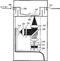
도 13에, 본 실시예의 센서 칩을 포함하는 분석 장치의 구성예를 나타낸다. 이 분석 장치(넓은 의미로는 분광 장치)는 센서 칩(300)(광 디바이스), 광원(310), 컬리메이트 렌즈(320), 편광 제어 소자(330), 대물 렌즈(350)(제 1 광학계), 다이클로익 미러(340), 집광 렌즈(360), 에탈론(370)(넓은 의미로는, 340, 360, 370는 제 2 광학계), 광 검출기(380)(검출기), 반송부(420)를 포함한다. 한편, 본 실시예의 분석 장치는 도 13의 구성으로 한정되지 않고, 그 구성 요소의 일부(예컨대 반송부)를 생략하거나, 다른 구성 요소를 추가하는 등의 여러가지 변형 실시가 가능하다. 13 shows an example of the configuration of an analysis device including the sensor chip of the present embodiment. This analysis device (a broad spectroscopic device) comprises a sensor chip 300 (optical device), a
광원(310)은, 표면 플라즈몬 폴라리톤과 표면 증강 라만 산란을 여기하는 레이저광을 출사한다. 광원(310)으로부터 출사된 레이저광은 컬리메이터 렌즈(320)에 의해 평행광으로 되고, 편광 제어 소자(330)에 의해 직선 편광으로 된다. 편광 제어 소자(330)를 통과한 레이저광은 다이클로익 미러(340)에 의해 센서 칩(300)의 방향으로 유도되고, 대물 렌즈(350)에서 집광되어, 센서 칩(300)에 입사한다. 센서 칩(300)의 표면에는, 예컨대 금속 격자나 검출 물질 선택 기구가 형성된다. 이 금속 격자의 주기는 레이저광의 파장보다 짧다. The
도 8에 나타내는 화살표는 표적물의 반송 방향을 나타낸다. 표적물은 팬(fan)(도시 생략)의 구동을 제어함으로써 반입구(400)로부터 반송부(420) 내부로 도입되고, 배출구(410)로부터 반송부(420) 외부로 배출된다. 이 때, 반송부(420)를 통과하는 표적물의 일부가 지지부(430)로 지지된 센서 칩(300)에 부착하고, 센서 칩(300)의 표면에 표적물(도시 생략)이 배치된다. The arrow shown in FIG. 8 shows the conveyance direction of a target. The target is introduced into the conveying
금속 격자 표면에 레이저광이 입사하면, 레이저광의 진동에 동반하여 자유 전자가 공명 진동하고, 금속 격자 표면 근방에는 표면 플라즈몬 폴라리톤을 통해서 매우 강한 증강 전장이 생긴다. 이 증강 전장에 예컨대 1~수개의 표적 물질이 침입하면, 여기서 표면 증강 라만 산란이 발생한다. 센서 칩(300)으로부터의 레일리-산란광과 라만 산란광은, 대물 렌즈(350)를 통과하고, 다이클로익 미러(340)에 의해서 광 검출기(380) 방향으로 유도된다. 이 산란광은, 집광 렌즈(360)로 집광되고, 에탈론(370)(분광기)을 통과해서, 광 검출기(380)에 입사한다. 그리고, 에탈론(370)에 의해 산란광으로부터 라만 산란광이 분광되고, 광 검출기(380)에 의해 이 라만 산란광이 수광된다. 이렇게 해서, 산란광이 스펙트럼 분해되고, 표적물의 스펙트럼 정보를 얻을 수 있다. When the laser beam is incident on the surface of the metal lattice, free electrons resonate with vibration of the laser beam, and a very strong enhanced electric field is generated through the surface plasmon polaritone near the surface of the metal lattice. When one to several target substances invade this enhanced electric field, for example, surface enhanced Raman scattering occurs. Rayleigh-scattered light and Raman scattered light from the
이상의 분석 장치에 의하면, 상술한 센서 칩(300)을 구비함으로써 표면 증강 라만 산란을 생기게 하고, 이 라만 산란광을 선택적으로 분광하여, 표적물을 검출할 수 있다. 이로써, 센서 감도의 향상을 도모하여, 표면 증강 라만 산란 스펙트럼으로부터 표적물을 특정하는 것이 가능해진다. According to the above analysis apparatus, by providing the
한편, 본 실시예의 분석 장치는, 마약이나 폭발물의 검지, 의료나 건강 진단, 식품의 검사에 사용되는 센싱 장치에 널리 응용하는 것이 가능하다. 또한, 항원 항체 반응에 있어서의 항원의 흡착의 유무 등과 같이, 물질의 흡착의 유무를 검출하는 어피니티 센서 등으로서 이용할 수 있다. On the other hand, the analysis device of the present embodiment can be widely applied to a sensing device used for detection of drugs and explosives, medical or medical examination, and inspection of food. Moreover, it can use as an affinity sensor etc. which detect the presence or absence of the adsorption | suction of a substance, such as presence or absence of the adsorption of an antigen in antigen-antibody reaction.
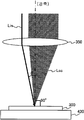
도 14에, 센서 칩에 입사광을 경사시켜서 입사시키기 위한 제 1 수법의 설명도를 나타낸다. 이 제 1 수법에서는, 입사빔 Lin(입사광)을 대물 렌즈(350)의 광축으로부터 어긋나서 입사함으로써, 센서 칩(300)에 대해 입사빔 Lin을 경사시킨다. 14, the explanatory drawing of the 1st method for making incident light incline to a sensor chip is shown. In this first method, the incident beam Lin is incident on the
구체적으로는, 대물 렌즈(350)의 광축에 대해 수직으로 센서 칩(300)을 지지부(430) 상에 배치한다. 그리고, 소정 거리만큼 대물 렌즈(350)의 광축으로부터 이격시켜서, 대물 렌즈(350)의 광축과 평행하게 입사빔 Lin을 입사시킨다. 소정 거리는, 센서 칩(300)에 대한 입사빔 Lin의 입사 각도가 대물 렌즈(350)의 굴절에 의해서 θ가 되는 거리이다. 센서 칩(300)으로부터의 산란광 Lsc(또는 반사광)은 대물 렌즈(350)에 입사되고, 대물 렌즈(350)에 의해서 다이클로익 미러(340) 등의 다음 단의 광학계로 유도된다. Specifically, the
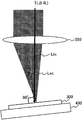
도 15에, 센서 칩에 입사광을 경사시켜서 입사시키기 위한 제 2 수법의 설명도를 나타낸다. 이 제 2 수법에서는, 입사빔 Lin(입사광)을 대물 렌즈(350)의 광축과 일치시켜서 입사시키는 한편, 대물 렌즈(350)의 광축에 대해 센서 칩(300)을 경사시켜서 배치함으로써, 센서 칩(300)에 대해 입사빔 Lin을 경사시킨다. 15 is an explanatory diagram of a second method for inclining incident light on the sensor chip and making it incident. In this second method, the incident beam Lin (incident light) coincides with the optical axis of the
구체적으로는, 센서 칩(300)의 평면(기재(100)의 평면)의 법선과, 대물 렌즈(350)의 광축이 이루는 각도를 θ로 배치한다. 그리고, 대물 렌즈(350)의 광축을 따라 입사빔 Lin을 입사시킨다. 그렇다면, 입사빔 Lin은 대물 렌즈(350)에 의해서 굴절되지 않고, 센서 칩(300)에 대해 입사 각도θ로 입사된다. 센서 칩(300)으로부터의 산란광 Lsc은, 상기 제 1 수법과 같이, 대물 렌즈(350)에 의해서 다음 단의 광학계로 유도된다. 한편, 본 실시예에서는 센서 칩(300)을 경사시키기 위해서, 도 15에 나타낸 바와 같이 지지부(430)를 경사시켜도 되고, 지지부(430)의 지지면을 경사면으로 해도 된다. Specifically, the angle between the normal of the plane of the sensor chip 300 (the plane of the base material 100) and the optical axis of the
한편, 상기한 바와 같이 본 실시예에 대해서 구체적으로 설명했지만, 본 발명의 신규 사항 및 효과로부터 실체적으로 일탈하지 않는 많은 변형이 가능하다는 것은 당업자에게는 용이하게 이해할 수 있을 것이다. 따라서, 이러한 변형예는 모두 본 발명의 범위에 포함되는 것으로 한다. 예컨대, 명세서 또는 도면에 있어서, 적어도 한번, 보다 넓은 의미 또는 같은 의미의 다른 용어(표적물, 입사광, 회절 격자, 전도체 등)와 같이 기재된 용어(표적 물질, 여기광, 금속 격자, 금속 등)는 명세서 또는 도면의 어떠한 개소에 있어서도, 이와 같은 용어로 바꿀 수 있다. 또한 광 디바이스, 분석 장치 등의 구성, 동작도 본 실시예에서 설명한 것에 한정되지 않고, 여러가지의 변형 실시가 가능하다.
On the other hand, while the present embodiment has been described in detail as described above, it will be readily understood by those skilled in the art that many modifications are possible without departing substantially from the novelty and effects of the present invention. Therefore, all such modifications shall fall within the scope of the present invention. For example, in the specification or drawings, the terms (target material, excitation light, metal lattice, metal, etc.) described at least once, such as broader or other terms of the same meaning (target, incident light, diffraction grating, conductor, etc.) In any place of a specification or drawing, it can replace with such a term. In addition, the structure and operation | movement of an optical device, an analysis apparatus, etc. are not limited to what was demonstrated by this embodiment, A various deformation | transformation can be implemented.
10 : 투명 기판 20 : 금속 미립자
100 : 기재 110 : 제 1 돌기군
120 : 기재의 표면 130 : 유리 기판
140 : 금속 박막 150 : 금속 격자
200 : 제 2 돌기군 210 : 제 3 돌기군
220 : 제 1 돌기군의 정상면
230 : 제 1 돌기군의 이웃하는 돌기 사이의 저면
300 : 센서 칩 310 :광원
320 : 컬리메이터 렌즈 330 : 편광 제어 소자
340 : 다이클로익 미러 350 : 대물 렌즈
360 : 집광 렌즈 370 : 에탈론
380 : 광 검출기 400 : 반입구
410 : 배출구 420 : 반송부
BW1 : 제 1 공명 피크 파장 대역 BW2 : 제 2 공명 피크 파장 대역
D1 : 제 1 방향 Lin : 입사광
Lsc : 산란광 P1 : 제 1 주기
P2 : 제 2 주기 P3 : 제 3 주기
Ram : 라만 산란광 Ray : 레일리-산란광
X : 표적 분자 θ : 입사 각도
λ1 : 여기 파장 λ2 : 라만 산란 파장
λin : 입사광의 파장 λp1 : 제 1 공명 피크 파장
λp2 : 제 2 공명 피크 파장 ω+, ω- : 공명 주파수10
100: base material 110: first projection group
120: surface of the substrate 130: glass substrate
140: metal thin film 150: metal grid
200: second projection group 210: third projection group
220: normal surface of the first protrusion group
230: Bottom between neighboring protrusions of the first protrusion group
300: sensor chip 310: light source
320: collimator lens 330: polarization control element
340: dichroic mirror 350: objective lens
360: condenser lens 370: etalon
380: photo detector 400: inlet
410: outlet 420: conveying unit
BW1: first resonance peak wavelength band BW2: second resonance peak wavelength band
D1: first direction Lin: incident light
Lsc: Scattered Light P1: First Cycle
P2: second cycle P3: third cycle
Ram: Raman scattered light Ray: Rayleigh-scattered light
X: target molecule θ: angle of incidence
λ1: excitation wavelength λ2: Raman scattering wavelength
λin: wavelength of incident light λp1: first resonance peak wavelength
λp2: second resonance peak wavelength ω +, ω-: resonance frequency
Claims (9)
상기 가상 평면을 향하는 수직선에 대하여 경사진 방향으로 진행하는 광을 상기 제 1 돌기군에 입사시킨 경우의 표면 플라즈몬 공명이, 제 1 공명 피크 파장과 제 2 공명 피크 파장 각각으로 발생하고,
상기 제 1 공명 피크 파장을 포함하는 제 1 공명 피크 파장 대역은, 상기 표면 증강 라만 산란에 있어서의 여기 파장 λ1을 포함하고,
상기 제 2 공명 피크 파장을 포함하는 제 2 공명 피크 파장 대역은, 상기 표면 증강 라만 산란에 있어서의 라만 산란 파장 λ2를 포함하는
것을 특징으로 하는 광 디바이스.
Has a first projection group in which the projections of the electrical conductor are arranged in a first period along a direction parallel to the imaginary plane,
Surface plasmon resonance when the light traveling in the direction inclined with respect to the vertical line toward the imaginary plane is incident on the first projection group, occurs at the first resonance peak wavelength and the second resonance peak wavelength, respectively.
The first resonance peak wavelength band including the first resonance peak wavelength includes an excitation wavelength λ1 in the surface enhancement Raman scattering,
The second resonance peak wavelength band including the second resonance peak wavelength includes a Raman scattering wavelength lambda 2 in the surface enhanced Raman scattering.
An optical device, characterized in that.
상기 라만 산란 파장 λ2는, 상기 여기 파장 λ1보다 긴 파장인 것을 특징으로 하는 광 디바이스.
The method of claim 1,
The said Raman scattering wavelength (lambda) 2 is a wavelength longer than the said excitation wavelength (lambda) 1.
상기 입사광으로서, 편광 방향의 상기 가상 평면에 평행한 성분과 상기 제 1 돌기군의 배열 방향이 평행한 직선 편광이 입사되는 것을 특징으로 하는 광 디바이스.
The method according to claim 1 or 2,
As said incident light, the linearly polarized light in which the component parallel to the said imaginary plane of a polarization direction, and the arrangement direction of the said 1st protrusion group in parallel are injected.
상기 제 1 돌기군의 정상면에, 전기 전도체에 의해 형성되는 제 2 돌기군을 포함하고,
상기 제 2 돌기군은, 상기 가상 평면에 평행한 방향을 따라서, 상기 제 1 주기보다 짧은 제 2 주기로 배열되는
것을 특징으로 하는 광 디바이스.
The method according to any one of claims 1 to 3,
On the top surface of the first projection group, including a second projection group formed by an electrical conductor,
The second projection group is arranged in a second period shorter than the first period along a direction parallel to the virtual plane.
An optical device, characterized in that.
상기 제 1 돌기군이 배열되는 면이며, 상기 제 1 돌기군의 이웃하는 돌기 사이의 면에, 전기 전도체에 의해 형성되는 제 3 돌기군을 포함하고,
상기 제 3 돌기군은, 상기 가상 평면에 평행한 방향을 따라서, 상기 제 1 주기보다 짧은 제 3 주기로 배열되는
것을 특징으로 하는 광 디바이스.
The method according to any one of claims 1 to 4,
The first protrusion group is a surface arranged, and includes a third protrusion group formed by an electric conductor on a surface between neighboring protrusions of the first protrusion group,
The third protrusion group is arranged in a third period shorter than the first period along a direction parallel to the virtual plane.
An optical device, characterized in that.
청구항 1 내지 청구항 5 중 어느 한 항에 기재된 광 디바이스와,
상기 광원으로부터의 상기 파장 λ1의 입사광을, 상기 광 디바이스의 상기 가상 평면을 향하는 수직선에 대해서 경사시켜서, 상기 전기 전도체의 격자에 입사시키는 제 1 광학계와,
상기 광 디바이스의 상기 전기 전도체의 격자에 의해 산란 또는 반사된 광 중에서 라만 산란광을 취출하는 제 2 광학계와,
상기 제 2 광학계를 통해서 수광된 상기 라만 산란광을 검출하는 검출기
를 포함하는 것을 특징으로 하는 분석 장치.
Light source,
The optical device according to any one of claims 1 to 5,
A first optical system in which the incident light of the wavelength? 1 from the light source is inclined with respect to the vertical line toward the imaginary plane of the optical device and is incident on the grating of the electric conductor;
A second optical system for extracting Raman scattered light from light scattered or reflected by the grating of the electrical conductor of the optical device,
A detector for detecting the Raman scattered light received through the second optical system
Analysis device comprising a.
상기 제 1 광학계는, 상기 입사광을 상기 제 1 광학계의 광축으로부터 어긋나게 해서 입사시킴으로써, 상기 입사광을 상기 가상 평면을 향하는 수직선에 대해 경사시켜서 상기 전기 전도체의 격자에 입사시키는 것을 특징으로 하는 분석 장치.
The method according to claim 6,
And the first optical system is incident by shifting the incident light from the optical axis of the first optical system, thereby inclining the incident light with respect to a vertical line directed to the virtual plane, and entering the grating of the electrical conductor.
상기 광 디바이스의 상기 가상 평면을 향하는 수직선이 상기 제 1 광학계의 광축에 대해 경사지도록, 상기 광 디바이스를 지지하는 지지부를 더 포함하고,
상기 제 1 광학계는, 상기 입사광을 상기 제 1 광학계의 광축과 일치시켜서 입사시킴으로써, 상기 입사광을 상기 가상 평면을 향하는 수직선에 대해서 경사시켜서, 상기 전기 전도체의 격자에 입사시키는 것
을 특징으로 하는 분석 장치.
The method according to claim 6,
And a support for supporting the optical device such that a vertical line facing the virtual plane of the optical device is inclined with respect to the optical axis of the first optical system,
Wherein the first optical system is incident to the incident light by coinciding the incident light with the optical axis of the first optical system, thereby inclining the incident light with respect to a vertical line facing the virtual plane, and incident the incident light into the grating of the electrical conductor.
Analysis device characterized in that.
상기 가상 평면을 향하는 수직선에 대하여 경사진 방향으로 진행하는 광을, 상기 제 1 돌기군에 입사시켜서, 제 1 공명 피크 파장과 제 2 공명 피크 파장의 각각으로 표면 플라즈몬 공명을 발생시키며,
상기 제 1 공명 피크 파장을 포함하는 제 1 공명 피크 파장 대역은, 상기 표면 증강 라만 산란에 있어서의 여기 파장 λ1을 포함하고,
상기 제 2 공명 피크 파장을 포함하는 제 2 공명 피크 파장 대역은, 상기 표면 증강 라만 산란에 있어서의 라만 산란 파장 λ2를 포함하는 것
을 특징으로 하는 분광 방법. Preparing a first projection group in which the projections of the electrical conductor are arranged in a first period along a direction parallel to the imaginary plane,
Light propagating in a direction inclined with respect to the vertical line toward the imaginary plane is incident on the first projection group to generate surface plasmon resonance at each of a first resonance peak wavelength and a second resonance peak wavelength,
The first resonance peak wavelength band including the first resonance peak wavelength includes an excitation wavelength λ1 in the surface enhancement Raman scattering,
The second resonance peak wavelength band including the second resonance peak wavelength includes Raman scattering wavelength λ2 in the surface enhancement Raman scattering.
Spectroscopic method characterized in that.
Applications Claiming Priority (2)
| Application Number | Priority Date | Filing Date | Title |
|---|---|---|---|
| JPJP-P-2010-103035 | 2010-04-28 | ||
| JP2010103035A JP5609241B2 (en) | 2010-04-28 | 2010-04-28 | Spectroscopic method and analyzer |
Publications (1)
| Publication Number | Publication Date |
|---|---|
| KR20110120233A true KR20110120233A (en) | 2011-11-03 |
Family
ID=44317620
Family Applications (1)
| Application Number | Title | Priority Date | Filing Date |
|---|---|---|---|
| KR20110039320A KR20110120233A (en) | 2010-04-28 | 2011-04-27 | Optical device, analyzer and spectroscopy method |
Country Status (6)
| Country | Link |
|---|---|
| US (1) | US8848182B2 (en) |
| EP (1) | EP2383565A1 (en) |
| JP (1) | JP5609241B2 (en) |
| KR (1) | KR20110120233A (en) |
| CN (1) | CN102608823B (en) |
| TW (1) | TWI567375B (en) |
Cited By (2)
| Publication number | Priority date | Publication date | Assignee | Title |
|---|---|---|---|---|
| KR101333482B1 (en) * | 2012-03-08 | 2013-11-26 | 단국대학교 산학협력단 | Measuring system for biological materials based on Surface Plasmon Scattering and Resonance |
| KR101494679B1 (en) * | 2013-12-30 | 2015-02-24 | 한국과학기술원 | Selection Method of Localized Surface Plasmon Resonance Wavelength for High Intense Surface Enhanced Raman Scattering |
Families Citing this family (20)
| Publication number | Priority date | Publication date | Assignee | Title |
|---|---|---|---|---|
| JP5560891B2 (en) * | 2010-05-13 | 2014-07-30 | セイコーエプソン株式会社 | Optical device and analyzer |
| JP5821511B2 (en) | 2011-10-17 | 2015-11-24 | セイコーエプソン株式会社 | Optical device and detection apparatus |
| JP5928026B2 (en) * | 2012-03-15 | 2016-06-01 | セイコーエプソン株式会社 | Sensor chip, manufacturing method thereof, and detection apparatus |
| JP2013234941A (en) * | 2012-05-10 | 2013-11-21 | Seiko Epson Corp | Sensor chip, sensor cartridge, and detector |
| JP2014169955A (en) | 2013-03-05 | 2014-09-18 | Seiko Epson Corp | Analysis device, analysis method, optical element and electronic apparatus used in them, and design method of optical element |
| JP2014206463A (en) * | 2013-04-12 | 2014-10-30 | 日本精工株式会社 | Target substance capture device |
| JP6180834B2 (en) * | 2013-07-24 | 2017-08-16 | 株式会社クラレ | Plasmon resonance structure |
| US9297772B2 (en) | 2013-07-30 | 2016-03-29 | Industrial Technology Research Institute | Apparatus for amplifying intensity during transmission small angle—X-ray scattering measurements |
| JP6269008B2 (en) * | 2013-12-12 | 2018-01-31 | 株式会社豊田中央研究所 | Electromagnetic wave-surface polariton conversion element. |
| JP6365817B2 (en) | 2014-02-17 | 2018-08-01 | セイコーエプソン株式会社 | Analytical device and electronic device |
| JP2015152492A (en) * | 2014-02-17 | 2015-08-24 | セイコーエプソン株式会社 | Analysis device and electronic apparatus |
| JP2016142617A (en) * | 2015-02-02 | 2016-08-08 | セイコーエプソン株式会社 | Electric field enhancement element, analyzer, and electronic apparatus |
| JP6613736B2 (en) * | 2015-09-07 | 2019-12-04 | セイコーエプソン株式会社 | Substance detection method and substance detection apparatus |
| US9772290B2 (en) | 2015-10-23 | 2017-09-26 | King Fahd University Of Petroleum And Minerals | Anisotropic monolayer gold nanoassembly: a highly SERS-active substrate for molecular detection |
| CN106125175A (en) * | 2016-06-24 | 2016-11-16 | 中国科学院长春光学精密机械与物理研究所 | A kind of slower rays structure, absorbency detection method and micro-fluidic chip |
| CN110291429A (en) * | 2017-01-30 | 2019-09-27 | 阿尔托大学基金会 | Phasmon device |
| CN110244392B (en) * | 2019-07-31 | 2021-07-20 | 华中科技大学 | Asymmetric transmitter |
| JP7210067B2 (en) * | 2019-08-02 | 2023-01-23 | 国立研究開発法人物質・材料研究機構 | Optical sensor, sensor unit, and object detection device using optical sensor |
| JP2022134422A (en) * | 2021-03-03 | 2022-09-15 | 株式会社日立ハイテク | Spectroscopic measurement device |
| US11959859B2 (en) * | 2021-06-02 | 2024-04-16 | Edwin Thomas Carlen | Multi-gas detection system and method |
Family Cites Families (16)
| Publication number | Priority date | Publication date | Assignee | Title |
|---|---|---|---|---|
| US6180415B1 (en) * | 1997-02-20 | 2001-01-30 | The Regents Of The University Of California | Plasmon resonant particles, methods and apparatus |
| JP3452837B2 (en) | 1999-06-14 | 2003-10-06 | 理化学研究所 | Localized plasmon resonance sensor |
| JP2005016963A (en) * | 2003-06-23 | 2005-01-20 | Canon Inc | Chemical sensor, and chemical sensor device |
| GB2418017A (en) * | 2004-09-10 | 2006-03-15 | Univ Southampton | Raman spectroscopy |
| JP2006093055A (en) | 2004-09-27 | 2006-04-06 | Toshiba Corp | Image display device |
| GB0424458D0 (en) * | 2004-11-04 | 2004-12-08 | Mesophotonics Ltd | Metal nano-void photonic crystal for enhanced raman spectroscopy |
| CN101057132B (en) | 2004-11-04 | 2012-04-18 | 雷尼绍诊断有限公司 | Metal nano-void photonic crystal for enhanced raman spectroscopy |
| WO2006093055A1 (en) * | 2005-03-03 | 2006-09-08 | National Institute For Materials Science | Chip for optical analysis, method for manufacturing the same, optical analyzer, and optical analyzing method |
| US7599066B2 (en) | 2005-06-01 | 2009-10-06 | Canon Kabushiki Kaisha | Localized plasmon resonance sensor |
| JP4878216B2 (en) * | 2005-06-01 | 2012-02-15 | キヤノン株式会社 | Local plasmon resonance sensor and detection method using local plasmon resonance sensor |
| TWI296044B (en) * | 2005-11-03 | 2008-04-21 | Ind Tech Res Inst | Coupled waveguide-surface plasmon resonance biosensor |
| WO2008073601A2 (en) * | 2006-10-31 | 2008-06-19 | Trustees Of Boston University | Deterministic aperiodic patterned dielectric and plasmonic materials for localized electromagnetic field enhancement |
| US7397559B1 (en) * | 2007-01-23 | 2008-07-08 | Hewlett-Packard Development Company, L.P. | Surface plasmon enhanced Raman spectroscopy |
| JP2009250951A (en) * | 2008-04-11 | 2009-10-29 | Fujifilm Corp | Electric field enhancement optical device |
| US8223331B2 (en) * | 2009-06-19 | 2012-07-17 | Hewlett-Packard Development Company, L.P. | Signal-amplification device for surface enhanced raman spectroscopy |
| US8865402B2 (en) * | 2009-08-26 | 2014-10-21 | Clemson University Research Foundation | Nanostructured substrates for surface enhanced raman spectroscopy (SERS) and detection of biological and chemical analytes by electrical double layer (EDL) capacitance |
-
2010
- 2010-04-28 JP JP2010103035A patent/JP5609241B2/en active Active
-
2011
- 2011-04-25 TW TW100114336A patent/TWI567375B/en active
- 2011-04-27 US US13/095,103 patent/US8848182B2/en active Active
- 2011-04-27 KR KR20110039320A patent/KR20110120233A/en not_active Application Discontinuation
- 2011-04-27 CN CN201110107698.3A patent/CN102608823B/en active Active
- 2011-04-28 EP EP20110164070 patent/EP2383565A1/en not_active Withdrawn
Cited By (2)
| Publication number | Priority date | Publication date | Assignee | Title |
|---|---|---|---|---|
| KR101333482B1 (en) * | 2012-03-08 | 2013-11-26 | 단국대학교 산학협력단 | Measuring system for biological materials based on Surface Plasmon Scattering and Resonance |
| KR101494679B1 (en) * | 2013-12-30 | 2015-02-24 | 한국과학기술원 | Selection Method of Localized Surface Plasmon Resonance Wavelength for High Intense Surface Enhanced Raman Scattering |
Also Published As
| Publication number | Publication date |
|---|---|
| CN102608823A (en) | 2012-07-25 |
| US8848182B2 (en) | 2014-09-30 |
| US20110267613A1 (en) | 2011-11-03 |
| TW201213791A (en) | 2012-04-01 |
| JP5609241B2 (en) | 2014-10-22 |
| EP2383565A1 (en) | 2011-11-02 |
| TWI567375B (en) | 2017-01-21 |
| JP2011232186A (en) | 2011-11-17 |
| CN102608823B (en) | 2016-02-03 |
Similar Documents
| Publication | Publication Date | Title |
|---|---|---|
| JP5609241B2 (en) | Spectroscopic method and analyzer | |
| US7151599B2 (en) | Monolithic system and method for enhanced Raman spectroscopy | |
| US7639355B2 (en) | Electric-field-enhancement structure and detection apparatus using same | |
| TWI506270B (en) | Optical device and analyzing apparatus | |
| US9057697B2 (en) | Optical device with propagating and localized surface plasmons and detection apparatus | |
| JP5589656B2 (en) | Sensor chip, sensor cartridge and analyzer | |
| JP5939016B2 (en) | Optical device and detection apparatus | |
| US7136160B2 (en) | Integrated system and method for transversal enhanced Raman Spectroscopy | |
| JP5621394B2 (en) | Sensor chip, sensor cartridge and analyzer | |
| JP5935492B2 (en) | Optical device and detection apparatus | |
| JP2015152492A (en) | Analysis device and electronic apparatus | |
| JP2013096939A (en) | Optical device and detector | |
| TWI453398B (en) | Sensor chip, sensor cartridge, and analysis apparatus | |
| Canpean et al. | Multifunctional plasmonic sensors on low-cost subwavelength metallic nanoholes arrays | |
| EP3051277A2 (en) | Electric-field enhancement element, analysis device, and eletronic apparatus | |
| JP5831583B2 (en) | Analysis equipment | |
| KR101669289B1 (en) | Sensor chip, sensor cartridge, and analysis apparatus | |
| JP2016003858A (en) | Detector, method for detection, and electric field enhancement element |
Legal Events
| Date | Code | Title | Description |
|---|---|---|---|
| WITN | Application deemed withdrawn, e.g. because no request for examination was filed or no examination fee was paid |