KR20110110240A - Antireflective articles and methods of making the same - Google Patents
Antireflective articles and methods of making the same Download PDFInfo
- Publication number
- KR20110110240A KR20110110240A KR1020117017517A KR20117017517A KR20110110240A KR 20110110240 A KR20110110240 A KR 20110110240A KR 1020117017517 A KR1020117017517 A KR 1020117017517A KR 20117017517 A KR20117017517 A KR 20117017517A KR 20110110240 A KR20110110240 A KR 20110110240A
- Authority
- KR
- South Korea
- Prior art keywords
- substrate
- matrix
- composite
- meth
- electrode
- Prior art date
Links
Images


Classifications
-
- G—PHYSICS
- G02—OPTICS
- G02B—OPTICAL ELEMENTS, SYSTEMS OR APPARATUS
- G02B1/00—Optical elements characterised by the material of which they are made; Optical coatings for optical elements
- G02B1/10—Optical coatings produced by application to, or surface treatment of, optical elements
- G02B1/11—Anti-reflection coatings
- G02B1/118—Anti-reflection coatings having sub-optical wavelength surface structures designed to provide an enhanced transmittance, e.g. moth-eye structures
-
- B—PERFORMING OPERATIONS; TRANSPORTING
- B05—SPRAYING OR ATOMISING IN GENERAL; APPLYING FLUENT MATERIALS TO SURFACES, IN GENERAL
- B05D—PROCESSES FOR APPLYING FLUENT MATERIALS TO SURFACES, IN GENERAL
- B05D3/00—Pretreatment of surfaces to which liquids or other fluent materials are to be applied; After-treatment of applied coatings, e.g. intermediate treating of an applied coating preparatory to subsequent applications of liquids or other fluent materials
- B05D3/10—Pretreatment of surfaces to which liquids or other fluent materials are to be applied; After-treatment of applied coatings, e.g. intermediate treating of an applied coating preparatory to subsequent applications of liquids or other fluent materials by other chemical means
- B05D3/107—Post-treatment of applied coatings
-
- B—PERFORMING OPERATIONS; TRANSPORTING
- B05—SPRAYING OR ATOMISING IN GENERAL; APPLYING FLUENT MATERIALS TO SURFACES, IN GENERAL
- B05D—PROCESSES FOR APPLYING FLUENT MATERIALS TO SURFACES, IN GENERAL
- B05D5/00—Processes for applying liquids or other fluent materials to surfaces to obtain special surface effects, finishes or structures
- B05D5/06—Processes for applying liquids or other fluent materials to surfaces to obtain special surface effects, finishes or structures to obtain multicolour or other optical effects
-
- B—PERFORMING OPERATIONS; TRANSPORTING
- B32—LAYERED PRODUCTS
- B32B—LAYERED PRODUCTS, i.e. PRODUCTS BUILT-UP OF STRATA OF FLAT OR NON-FLAT, e.g. CELLULAR OR HONEYCOMB, FORM
- B32B17/00—Layered products essentially comprising sheet glass, or glass, slag, or like fibres
- B32B17/06—Layered products essentially comprising sheet glass, or glass, slag, or like fibres comprising glass as the main or only constituent of a layer, next to another layer of a specific material
-
- B—PERFORMING OPERATIONS; TRANSPORTING
- B32—LAYERED PRODUCTS
- B32B—LAYERED PRODUCTS, i.e. PRODUCTS BUILT-UP OF STRATA OF FLAT OR NON-FLAT, e.g. CELLULAR OR HONEYCOMB, FORM
- B32B37/00—Methods or apparatus for laminating, e.g. by curing or by ultrasonic bonding
- B32B37/02—Methods or apparatus for laminating, e.g. by curing or by ultrasonic bonding characterised by a sequence of laminating steps, e.g. by adding new layers at consecutive laminating stations
-
- B—PERFORMING OPERATIONS; TRANSPORTING
- B32—LAYERED PRODUCTS
- B32B—LAYERED PRODUCTS, i.e. PRODUCTS BUILT-UP OF STRATA OF FLAT OR NON-FLAT, e.g. CELLULAR OR HONEYCOMB, FORM
- B32B38/00—Ancillary operations in connection with laminating processes
- B32B38/0008—Electrical discharge treatment, e.g. corona, plasma treatment; wave energy or particle radiation
-
- B—PERFORMING OPERATIONS; TRANSPORTING
- B32—LAYERED PRODUCTS
- B32B—LAYERED PRODUCTS, i.e. PRODUCTS BUILT-UP OF STRATA OF FLAT OR NON-FLAT, e.g. CELLULAR OR HONEYCOMB, FORM
- B32B7/00—Layered products characterised by the relation between layers; Layered products characterised by the relative orientation of features between layers, or by the relative values of a measurable parameter between layers, i.e. products comprising layers having different physical, chemical or physicochemical properties; Layered products characterised by the interconnection of layers
- B32B7/04—Interconnection of layers
- B32B7/12—Interconnection of layers using interposed adhesives or interposed materials with bonding properties
-
- C—CHEMISTRY; METALLURGY
- C08—ORGANIC MACROMOLECULAR COMPOUNDS; THEIR PREPARATION OR CHEMICAL WORKING-UP; COMPOSITIONS BASED THEREON
- C08J—WORKING-UP; GENERAL PROCESSES OF COMPOUNDING; AFTER-TREATMENT NOT COVERED BY SUBCLASSES C08B, C08C, C08F, C08G or C08H
- C08J7/00—Chemical treatment or coating of shaped articles made of macromolecular substances
- C08J7/04—Coating
- C08J7/042—Coating with two or more layers, where at least one layer of a composition contains a polymer binder
- C08J7/0423—Coating with two or more layers, where at least one layer of a composition contains a polymer binder with at least one layer of inorganic material and at least one layer of a composition containing a polymer binder
-
- C—CHEMISTRY; METALLURGY
- C08—ORGANIC MACROMOLECULAR COMPOUNDS; THEIR PREPARATION OR CHEMICAL WORKING-UP; COMPOSITIONS BASED THEREON
- C08J—WORKING-UP; GENERAL PROCESSES OF COMPOUNDING; AFTER-TREATMENT NOT COVERED BY SUBCLASSES C08B, C08C, C08F, C08G or C08H
- C08J7/00—Chemical treatment or coating of shaped articles made of macromolecular substances
- C08J7/04—Coating
- C08J7/043—Improving the adhesiveness of the coatings per se, e.g. forming primers
-
- C—CHEMISTRY; METALLURGY
- C08—ORGANIC MACROMOLECULAR COMPOUNDS; THEIR PREPARATION OR CHEMICAL WORKING-UP; COMPOSITIONS BASED THEREON
- C08J—WORKING-UP; GENERAL PROCESSES OF COMPOUNDING; AFTER-TREATMENT NOT COVERED BY SUBCLASSES C08B, C08C, C08F, C08G or C08H
- C08J7/00—Chemical treatment or coating of shaped articles made of macromolecular substances
- C08J7/04—Coating
- C08J7/044—Forming conductive coatings; Forming coatings having anti-static properties
-
- C—CHEMISTRY; METALLURGY
- C08—ORGANIC MACROMOLECULAR COMPOUNDS; THEIR PREPARATION OR CHEMICAL WORKING-UP; COMPOSITIONS BASED THEREON
- C08J—WORKING-UP; GENERAL PROCESSES OF COMPOUNDING; AFTER-TREATMENT NOT COVERED BY SUBCLASSES C08B, C08C, C08F, C08G or C08H
- C08J7/00—Chemical treatment or coating of shaped articles made of macromolecular substances
- C08J7/04—Coating
- C08J7/046—Forming abrasion-resistant coatings; Forming surface-hardening coatings
-
- C—CHEMISTRY; METALLURGY
- C08—ORGANIC MACROMOLECULAR COMPOUNDS; THEIR PREPARATION OR CHEMICAL WORKING-UP; COMPOSITIONS BASED THEREON
- C08J—WORKING-UP; GENERAL PROCESSES OF COMPOUNDING; AFTER-TREATMENT NOT COVERED BY SUBCLASSES C08B, C08C, C08F, C08G or C08H
- C08J7/00—Chemical treatment or coating of shaped articles made of macromolecular substances
- C08J7/04—Coating
- C08J7/054—Forming anti-misting or drip-proofing coatings
-
- C—CHEMISTRY; METALLURGY
- C08—ORGANIC MACROMOLECULAR COMPOUNDS; THEIR PREPARATION OR CHEMICAL WORKING-UP; COMPOSITIONS BASED THEREON
- C08J—WORKING-UP; GENERAL PROCESSES OF COMPOUNDING; AFTER-TREATMENT NOT COVERED BY SUBCLASSES C08B, C08C, C08F, C08G or C08H
- C08J7/00—Chemical treatment or coating of shaped articles made of macromolecular substances
- C08J7/04—Coating
- C08J7/056—Forming hydrophilic coatings
-
- C—CHEMISTRY; METALLURGY
- C08—ORGANIC MACROMOLECULAR COMPOUNDS; THEIR PREPARATION OR CHEMICAL WORKING-UP; COMPOSITIONS BASED THEREON
- C08J—WORKING-UP; GENERAL PROCESSES OF COMPOUNDING; AFTER-TREATMENT NOT COVERED BY SUBCLASSES C08B, C08C, C08F, C08G or C08H
- C08J7/00—Chemical treatment or coating of shaped articles made of macromolecular substances
- C08J7/12—Chemical modification
- C08J7/123—Treatment by wave energy or particle radiation
-
- G—PHYSICS
- G02—OPTICS
- G02B—OPTICAL ELEMENTS, SYSTEMS OR APPARATUS
- G02B1/00—Optical elements characterised by the material of which they are made; Optical coatings for optical elements
- G02B1/10—Optical coatings produced by application to, or surface treatment of, optical elements
- G02B1/11—Anti-reflection coatings
- G02B1/111—Anti-reflection coatings using layers comprising organic materials
-
- G—PHYSICS
- G02—OPTICS
- G02B—OPTICAL ELEMENTS, SYSTEMS OR APPARATUS
- G02B1/00—Optical elements characterised by the material of which they are made; Optical coatings for optical elements
- G02B1/10—Optical coatings produced by application to, or surface treatment of, optical elements
- G02B1/12—Optical coatings produced by application to, or surface treatment of, optical elements by surface treatment, e.g. by irradiation
-
- G—PHYSICS
- G02—OPTICS
- G02B—OPTICAL ELEMENTS, SYSTEMS OR APPARATUS
- G02B1/00—Optical elements characterised by the material of which they are made; Optical coatings for optical elements
- G02B1/10—Optical coatings produced by application to, or surface treatment of, optical elements
- G02B1/14—Protective coatings, e.g. hard coatings
-
- G—PHYSICS
- G02—OPTICS
- G02B—OPTICAL ELEMENTS, SYSTEMS OR APPARATUS
- G02B1/00—Optical elements characterised by the material of which they are made; Optical coatings for optical elements
- G02B1/10—Optical coatings produced by application to, or surface treatment of, optical elements
- G02B1/18—Coatings for keeping optical surfaces clean, e.g. hydrophobic or photo-catalytic films
-
- G—PHYSICS
- G02—OPTICS
- G02B—OPTICAL ELEMENTS, SYSTEMS OR APPARATUS
- G02B27/00—Optical systems or apparatus not provided for by any of the groups G02B1/00 - G02B26/00, G02B30/00
- G02B27/0006—Optical systems or apparatus not provided for by any of the groups G02B1/00 - G02B26/00, G02B30/00 with means to keep optical surfaces clean, e.g. by preventing or removing dirt, stains, contamination, condensation
-
- B—PERFORMING OPERATIONS; TRANSPORTING
- B32—LAYERED PRODUCTS
- B32B—LAYERED PRODUCTS, i.e. PRODUCTS BUILT-UP OF STRATA OF FLAT OR NON-FLAT, e.g. CELLULAR OR HONEYCOMB, FORM
- B32B2255/00—Coating on the layer surface
- B32B2255/26—Polymeric coating
-
- B—PERFORMING OPERATIONS; TRANSPORTING
- B32—LAYERED PRODUCTS
- B32B—LAYERED PRODUCTS, i.e. PRODUCTS BUILT-UP OF STRATA OF FLAT OR NON-FLAT, e.g. CELLULAR OR HONEYCOMB, FORM
- B32B2307/00—Properties of the layers or laminate
- B32B2307/40—Properties of the layers or laminate having particular optical properties
- B32B2307/412—Transparent
-
- B—PERFORMING OPERATIONS; TRANSPORTING
- B32—LAYERED PRODUCTS
- B32B—LAYERED PRODUCTS, i.e. PRODUCTS BUILT-UP OF STRATA OF FLAT OR NON-FLAT, e.g. CELLULAR OR HONEYCOMB, FORM
- B32B2307/00—Properties of the layers or laminate
- B32B2307/40—Properties of the layers or laminate having particular optical properties
- B32B2307/42—Polarizing, birefringent, filtering
-
- B—PERFORMING OPERATIONS; TRANSPORTING
- B32—LAYERED PRODUCTS
- B32B—LAYERED PRODUCTS, i.e. PRODUCTS BUILT-UP OF STRATA OF FLAT OR NON-FLAT, e.g. CELLULAR OR HONEYCOMB, FORM
- B32B2457/00—Electrical equipment
- B32B2457/20—Displays, e.g. liquid crystal displays, plasma displays
-
- B—PERFORMING OPERATIONS; TRANSPORTING
- B32—LAYERED PRODUCTS
- B32B—LAYERED PRODUCTS, i.e. PRODUCTS BUILT-UP OF STRATA OF FLAT OR NON-FLAT, e.g. CELLULAR OR HONEYCOMB, FORM
- B32B2457/00—Electrical equipment
- B32B2457/20—Displays, e.g. liquid crystal displays, plasma displays
- B32B2457/202—LCD, i.e. liquid crystal displays
-
- B—PERFORMING OPERATIONS; TRANSPORTING
- B32—LAYERED PRODUCTS
- B32B—LAYERED PRODUCTS, i.e. PRODUCTS BUILT-UP OF STRATA OF FLAT OR NON-FLAT, e.g. CELLULAR OR HONEYCOMB, FORM
- B32B2551/00—Optical elements
-
- C—CHEMISTRY; METALLURGY
- C08—ORGANIC MACROMOLECULAR COMPOUNDS; THEIR PREPARATION OR CHEMICAL WORKING-UP; COMPOSITIONS BASED THEREON
- C08J—WORKING-UP; GENERAL PROCESSES OF COMPOUNDING; AFTER-TREATMENT NOT COVERED BY SUBCLASSES C08B, C08C, C08F, C08G or C08H
- C08J2323/00—Characterised by the use of homopolymers or copolymers of unsaturated aliphatic hydrocarbons having only one carbon-to-carbon double bond; Derivatives of such polymers
- C08J2323/02—Characterised by the use of homopolymers or copolymers of unsaturated aliphatic hydrocarbons having only one carbon-to-carbon double bond; Derivatives of such polymers not modified by chemical after treatment
- C08J2323/04—Homopolymers or copolymers of ethene
- C08J2323/06—Polyethene
-
- C—CHEMISTRY; METALLURGY
- C08—ORGANIC MACROMOLECULAR COMPOUNDS; THEIR PREPARATION OR CHEMICAL WORKING-UP; COMPOSITIONS BASED THEREON
- C08J—WORKING-UP; GENERAL PROCESSES OF COMPOUNDING; AFTER-TREATMENT NOT COVERED BY SUBCLASSES C08B, C08C, C08F, C08G or C08H
- C08J2367/00—Characterised by the use of polyesters obtained by reactions forming a carboxylic ester link in the main chain; Derivatives of such polymers
- C08J2367/02—Polyesters derived from dicarboxylic acids and dihydroxy compounds
-
- C—CHEMISTRY; METALLURGY
- C08—ORGANIC MACROMOLECULAR COMPOUNDS; THEIR PREPARATION OR CHEMICAL WORKING-UP; COMPOSITIONS BASED THEREON
- C08J—WORKING-UP; GENERAL PROCESSES OF COMPOUNDING; AFTER-TREATMENT NOT COVERED BY SUBCLASSES C08B, C08C, C08F, C08G or C08H
- C08J2433/00—Characterised by the use of homopolymers or copolymers of compounds having one or more unsaturated aliphatic radicals, each having only one carbon-to-carbon double bond, and only one being terminated by only one carboxyl radical, or of salts, anhydrides, esters, amides, imides, or nitriles thereof; Derivatives of such polymers
- C08J2433/04—Characterised by the use of homopolymers or copolymers of compounds having one or more unsaturated aliphatic radicals, each having only one carbon-to-carbon double bond, and only one being terminated by only one carboxyl radical, or of salts, anhydrides, esters, amides, imides, or nitriles thereof; Derivatives of such polymers esters
- C08J2433/06—Characterised by the use of homopolymers or copolymers of compounds having one or more unsaturated aliphatic radicals, each having only one carbon-to-carbon double bond, and only one being terminated by only one carboxyl radical, or of salts, anhydrides, esters, amides, imides, or nitriles thereof; Derivatives of such polymers esters of esters containing only carbon, hydrogen, and oxygen, the oxygen atom being present only as part of the carboxyl radical
- C08J2433/08—Homopolymers or copolymers of acrylic acid esters
-
- C—CHEMISTRY; METALLURGY
- C08—ORGANIC MACROMOLECULAR COMPOUNDS; THEIR PREPARATION OR CHEMICAL WORKING-UP; COMPOSITIONS BASED THEREON
- C08J—WORKING-UP; GENERAL PROCESSES OF COMPOUNDING; AFTER-TREATMENT NOT COVERED BY SUBCLASSES C08B, C08C, C08F, C08G or C08H
- C08J2483/00—Characterised by the use of macromolecular compounds obtained by reactions forming in the main chain of the macromolecule a linkage containing silicon with or without sulfur, nitrogen, oxygen, or carbon only; Derivatives of such polymers
- C08J2483/02—Polysilicates
-
- F—MECHANICAL ENGINEERING; LIGHTING; HEATING; WEAPONS; BLASTING
- F24—HEATING; RANGES; VENTILATING
- F24S—SOLAR HEAT COLLECTORS; SOLAR HEAT SYSTEMS
- F24S70/00—Details of absorbing elements
- F24S70/10—Details of absorbing elements characterised by the absorbing material
-
- F—MECHANICAL ENGINEERING; LIGHTING; HEATING; WEAPONS; BLASTING
- F24—HEATING; RANGES; VENTILATING
- F24S—SOLAR HEAT COLLECTORS; SOLAR HEAT SYSTEMS
- F24S70/00—Details of absorbing elements
- F24S70/60—Details of absorbing elements characterised by the structure or construction
-
- Y—GENERAL TAGGING OF NEW TECHNOLOGICAL DEVELOPMENTS; GENERAL TAGGING OF CROSS-SECTIONAL TECHNOLOGIES SPANNING OVER SEVERAL SECTIONS OF THE IPC; TECHNICAL SUBJECTS COVERED BY FORMER USPC CROSS-REFERENCE ART COLLECTIONS [XRACs] AND DIGESTS
- Y10—TECHNICAL SUBJECTS COVERED BY FORMER USPC
- Y10T—TECHNICAL SUBJECTS COVERED BY FORMER US CLASSIFICATION
- Y10T428/00—Stock material or miscellaneous articles
- Y10T428/25—Web or sheet containing structurally defined element or component and including a second component containing structurally defined particles
- Y10T428/254—Polymeric or resinous material
-
- Y—GENERAL TAGGING OF NEW TECHNOLOGICAL DEVELOPMENTS; GENERAL TAGGING OF CROSS-SECTIONAL TECHNOLOGIES SPANNING OVER SEVERAL SECTIONS OF THE IPC; TECHNICAL SUBJECTS COVERED BY FORMER USPC CROSS-REFERENCE ART COLLECTIONS [XRACs] AND DIGESTS
- Y10—TECHNICAL SUBJECTS COVERED BY FORMER USPC
- Y10T—TECHNICAL SUBJECTS COVERED BY FORMER US CLASSIFICATION
- Y10T428/00—Stock material or miscellaneous articles
- Y10T428/25—Web or sheet containing structurally defined element or component and including a second component containing structurally defined particles
- Y10T428/256—Heavy metal or aluminum or compound thereof
- Y10T428/257—Iron oxide or aluminum oxide
-
- Y—GENERAL TAGGING OF NEW TECHNOLOGICAL DEVELOPMENTS; GENERAL TAGGING OF CROSS-SECTIONAL TECHNOLOGIES SPANNING OVER SEVERAL SECTIONS OF THE IPC; TECHNICAL SUBJECTS COVERED BY FORMER USPC CROSS-REFERENCE ART COLLECTIONS [XRACs] AND DIGESTS
- Y10—TECHNICAL SUBJECTS COVERED BY FORMER USPC
- Y10T—TECHNICAL SUBJECTS COVERED BY FORMER US CLASSIFICATION
- Y10T428/00—Stock material or miscellaneous articles
- Y10T428/25—Web or sheet containing structurally defined element or component and including a second component containing structurally defined particles
- Y10T428/258—Alkali metal or alkaline earth metal or compound thereof
-
- Y—GENERAL TAGGING OF NEW TECHNOLOGICAL DEVELOPMENTS; GENERAL TAGGING OF CROSS-SECTIONAL TECHNOLOGIES SPANNING OVER SEVERAL SECTIONS OF THE IPC; TECHNICAL SUBJECTS COVERED BY FORMER USPC CROSS-REFERENCE ART COLLECTIONS [XRACs] AND DIGESTS
- Y10—TECHNICAL SUBJECTS COVERED BY FORMER USPC
- Y10T—TECHNICAL SUBJECTS COVERED BY FORMER US CLASSIFICATION
- Y10T428/00—Stock material or miscellaneous articles
- Y10T428/25—Web or sheet containing structurally defined element or component and including a second component containing structurally defined particles
- Y10T428/259—Silicic material
-
- Y—GENERAL TAGGING OF NEW TECHNOLOGICAL DEVELOPMENTS; GENERAL TAGGING OF CROSS-SECTIONAL TECHNOLOGIES SPANNING OVER SEVERAL SECTIONS OF THE IPC; TECHNICAL SUBJECTS COVERED BY FORMER USPC CROSS-REFERENCE ART COLLECTIONS [XRACs] AND DIGESTS
- Y10—TECHNICAL SUBJECTS COVERED BY FORMER USPC
- Y10T—TECHNICAL SUBJECTS COVERED BY FORMER US CLASSIFICATION
- Y10T428/00—Stock material or miscellaneous articles
- Y10T428/28—Web or sheet containing structurally defined element or component and having an adhesive outermost layer
- Y10T428/2848—Three or more layers
Abstract
(a) 가시광에서 적어도 90% 투과율 및 5% 미만의 탁도(haze)를 가지며, 대향하는 제1 및 제2 표면을 가지는 기판, (b) 매트릭스 및 나노스케일 분산상을 포함하고, 무작위 나노구조 이방성 표면을 가지는 나노구조 용품, 및 (c) 기판의 제2 표면 상에 배치된 광학적으로 투명한 접착제를 가지는 복합체가 개시된다.(a) a substrate having at least 90% transmission in visible light and less than 5% haze, and having opposing first and second surfaces, (b) a matrix and a nanoscale dispersed phase, wherein the random nanostructure anisotropic surface A composite having a nanostructured article having an adhesive, and (c) an optically clear adhesive disposed on a second surface of the substrate is disclosed.
Description
(관련 출원의 상호 참조)(Cross-reference of related application)
이 출원은 미국 가특허 출원 제61/141,517호(2008년 12월 30일 출원); 제61/157,683호(2009년 3월 5일 출원); 및 제61/234,782호(2009년 8월 18일 출원) , 이들 각각은 전체로서 참조로 포함된다.This application is issued US Provisional Patent Application 61 / 141,517, filed December 30, 2008; 61 / 157,683 filed March 5, 2009; And 61 / 234,782 filed August 18, 2009, each of which is incorporated by reference in its entirety.
본 발명은 예를 들면 반사방지 용품으로서 유용한 나노구조 용품에 관한 것이다. 다른 태양에서, 이 발명은 나노구조 용품을 제조하는 방법에 관한 것이다.The present invention relates to nanostructured articles useful for example as antireflective articles. In another aspect, the invention relates to a method of making a nanostructured article.
하나의 매질에서 다른 매질로 광이 이동할 때마다, 광의 일부가 두 매질 사이의 계면으로부터 반사된다. 예를 들어, 투명한 가소성 기판 상에서 빛나는 광의 약 4 내지 5%가 상부 표면에서 반사된다.Each time light travels from one medium to another, a portion of the light is reflected from the interface between the two media. For example, about 4-5% of the light shining on the transparent plastic substrate is reflected at the top surface.
다른 접근법들이 폴리머 물질의 반사를 줄이기 위해 사용되어 왔다. 하나의 접근법은 반사를 줄이기 위해 대조적인 굴절률의 교대되는 층들을 포함하는 투명 박막 구조물로 구성된 다층 반사 코팅과 같은 반사방지(AR: antireflective) 코팅을 이용하는 것이다. 그러나, AR 코팅을 사용하여 광대역(broadband) 반사방지 효과를 얻는 것은 어렵다는 것이 입증되었다.Different approaches have been used to reduce the reflection of polymeric materials. One approach is to use an antireflective (AR) coating, such as a multilayer reflective coating composed of transparent thin film structures comprising alternating layers of contrasting refractive index to reduce reflection. However, it has proven difficult to achieve broadband antireflection effects using AR coatings.
다른 접근법은 광대역 반사방지를 위해 서브파장 표면 구조물(예를 들면, 서브파장 스케일 표면 격자)을 사용하는 것을 포함한다. 서브파장 표면 구조물을 생성하는 방법은 그러나, 복잡하고 비싼 배치 프로세스가 되는 경향이 있다. 예를 들어, 미국 특허 출원 공개 제2005/0233083호는 6.67 cPa (0.5 mTorr) 미만의 진공 조건 하에서 Ar/O2 플라스마로 폴리머 표면을 타격하는 것을 포함한다. 극단적인 진공 조건에 대한 이러한 요구는 이 방법의 상업적 실용성을 제한한다.Another approach involves using subwavelength surface structures (eg, subwavelength scale surface gratings) for broadband antireflection. The method of producing subwavelength surface structures, however, tends to be a complex and expensive placement process. For example, US Patent Application Publication No. 2005/0233083 includes hitting the polymer surface with Ar / O 2 plasma under vacuum conditions of less than 0.5 mTorr (6.67 cPa). This requirement for extreme vacuum conditions limits the commercial practicality of this method.
전술한 견지에서, 표면, 특히 폴리머 표면의 반사를 줄일 수 있는 대안적인 접근법에 대한 필요성이 존재한다는 것이 인식된다. 나아가, 표면의 반사를 줄이기 위한 접근법이 상업적 실용성을 갖기 위해서는, 상대적으로 간단하고 비싸지 않을 것이 요구된다는 것이 인식된다.In view of the foregoing, it is recognized that there is a need for alternative approaches that can reduce the reflection of surfaces, particularly polymer surfaces. Furthermore, it is recognized that an approach for reducing the reflection of the surface is required to be relatively simple and inexpensive in order to have commercial utility.
간단히, 일 태양에서, 본 발명은 매트릭스 및 나노스케일 분산상을 포함하고 무작위 나노구조 이방성 표면을 가지는 나노구조 용품을 제공한다.Briefly, in one aspect, the present invention provides a nanostructured article comprising a matrix and a nanoscale dispersed phase and having a random nanostructured anisotropic surface.
내용 중에 사용된 것과 같이, "나노스케일(nanoscale)"은 서브미크론(예를 들면, 약 1 nm 내지 500 nm)을 의미하고; "나노구조화된(nanostructured)"은 나노스케일 상에 일 차원을 가지는 것을 의미하며; 그리고 "이방성 표면(anisotropic surface)"은 약 1.5:1 이상(바람직하게는, 2:1 이상; 더 바람직하게는 5:1 이상)의 높이 대 폭(즉, 평균 폭) 비율을 가지는 구조적 거칠기(asperities)를 가지는 표면을 의미한다.As used in the context, “nanoscale” means submicron (eg, about 1 nm to 500 nm); "Nanostructured" means having one dimension on the nanoscale; And “anisotropic surface” is a structural roughness having a height-to-width (ie, average width) ratio of about 1.5: 1 or greater (preferably 2: 1 or greater; more preferably 5: 1 or greater). means a surface with asperities).
본 발명의 나노구조 용품은 동일한 매트릭스 물질 및 나노분산상을 포함하는 비구조화 용품에 비하여 반사에서 현저한 감소를 나타낸다. 또한, 본 발명의 나노구조 용품은 내구력이 있을 수 있고 스크래치 내성을 가질 수 있다. 또한, 본 발명의 나노구조 용품의 일부 실시예는 예를 들면, 김서림 방지, 쉬운 세정, 항미생물 활동성, 친수성 또는 소수성과 같은 추가적인 바람직한 속성을 나타낸다.The nanostructured articles of the invention exhibit a significant reduction in reflection compared to unstructured articles comprising the same matrix material and nanodispersed phase. In addition, the nanostructured articles of the present invention may be durable and scratch resistant. In addition, some embodiments of the nanostructured articles of the present invention exhibit additional desirable properties such as, for example, antifogging, easy cleaning, antimicrobial activity, hydrophilicity, or hydrophobicity.
다른 측면에서, 본 발명의 개시내용은 무작위 나노구조 표면을 제조하는 방법을 제공한다. 하나의 방법은 나노분산상을 포함하는 매트릭스를 제공하는 단계와, 무작위 나노구조 이방성 표면을 형성하기 위해 플라스마를 사용하여 매트릭스를 이방성 식각하는 단계를 포함한다. 다른 방법은 나노분산상을 포함하는 매트릭스를 제공하는 단계와, 무작위 나노구조 표면을 형성하기 위해 플라스마를 사용하는 나노분상상의 적어도 일부를 식각하는 단계를 포함한다.In another aspect, the present disclosure provides a method of making a random nanostructured surface. One method includes providing a matrix comprising nanodispersed phases and anisotropically etching the matrix using plasma to form a random nanostructured anisotropic surface. Another method includes providing a matrix comprising nanodispersed phases and etching at least a portion of the nanodispersed phases using plasma to form random nanostructured surfaces.
또 다른 태양에서, 본 발명의 개시내용은 다음을 포함하는 복합체를 제공한다: (a) 가시광에서 적어도 90%의 투과율 및 5% 미만의 탁도(haze)를 가지며, 대면하는 제 1 및 제 2 표면을 가지는 기판; (b) 기판의 제 1 표면 상에 배치되고, 매트릭스 및 나노스케일 분상상을 포함하며, 무작위 나노구조 이방성 표면을 가지는 나노구조 용품; 및 (c) 기판의 제 2 표면 상에 배치되며, 가시광에서 적어도 90%의 투과율 및 5% 미만의 탁도를 가지는 광학적으로 투명한(clear) 접착제.In another aspect, the present disclosure provides a composite comprising: (a) first and second facing surfaces having at least 90% transmission and less than 5% haze in visible light; A substrate having a; (b) a nanostructured article disposed on the first surface of the substrate and comprising a matrix and nanoscale phases and having a random nanostructured anisotropic surface; And (c) an optically clear adhesive disposed on the second surface of the substrate and having at least 90% transmission and less than 5% haze in visible light.
또 다른 측면에서, 본 발명의 개시내용은 다음의 단계를 포함하는 복합체를 제조하는 방법을 제공한다: (a) 가시광에서 적어도 90% 투과율 및 5% 미만의 탁도를 가지는 기판을 제공하는 단계; (b) 반사방지 층을 제조하기 위해 기판의 제1 주 표면 상에, SiO2, ZrO2 및 이들의 조합물로서, 매트릭스 에 분산된 나노입자를 포함하는 하드코트 조성물을 코팅하는 단계; (c) 반사방지 층을 산출하기 위해 하드코트 용액을 건조하는 단계; (d) (i) 진공 용기(vessel) 내의 실린더형 전극 상에 반사방지 층을 배치하는 단계, (ii) 사전지정된 압력에서 이 용기에 식각 가스를 도입하는 단계, (iii) 실린더형 전극 및 상대 전극 사이에 플라스마를 발생시키는 단계; (iv) 기판이 병진하도록 실린더형 전극을 회전시키는 단계; 및 (v) 하드코트 조성물을 이방성 식각하는 단계; 및 (e) 기판의 제2 표면에 배치되며, 가시광에서 적어도 90%의 투과율 및 5% 미만의 탁도를 가지는 광학적으로 투명한 접착제를 라미네이팅 하는 단계.In another aspect, the present disclosure provides a method of making a composite comprising the steps of: (a) providing a substrate having at least 90% transmission and less than 5% haze in visible light; (b) coating a hardcoat composition comprising nanoparticles dispersed in a matrix, as SiO 2 , ZrO 2, and combinations thereof, on the first major surface of the substrate to produce an antireflective layer; (c) drying the hardcoat solution to yield an antireflective layer; (d) (i) placing an antireflective layer on the cylindrical electrode in a vacuum vessel, (ii) introducing an etch gas into the vessel at a predetermined pressure, (iii) the cylindrical electrode and the counterpart Generating a plasma between the electrodes; (iv) rotating the cylindrical electrode to translate the substrate; And (v) anisotropically etching the hardcoat composition; And (e) laminating an optically clear adhesive disposed on the second surface of the substrate and having at least 90% transmittance and less than 5% haze in visible light.
내용 중에 사용된 것과 같이, "플라스마"는 전자, 이온, 중성 분자 및 자유 라디칼을 함유하는 부분적으로 이온화된 가스 또는 유체 상태의 재료를 의미한다.As used herein, "plasma" means a material in a partially ionized gas or fluid state containing electrons, ions, neutral molecules, and free radicals.
본 개시내용의 방법은 적당한 진공 조건(예를 들면, 약 66.7 cPa (5 mTorr) 내지 약 1.3 Pa (10 mTorr))에서 수행될 수 있다. 또한 이들은 실린더 반응성 이온 식각(실린더 RIE)을 사용하여 롤-투-롤(즉, 연속적) 프로세스로서 수행될 수 있다.The methods of the present disclosure can be performed at suitable vacuum conditions (eg, about 66.7 cPa (5 mTorr) to about 1.3 Pa (10 mTorr)). They can also be performed as a roll-to-roll (ie continuous) process using cylinder reactive ion etching (cylinder RIE).
본 발명의 개시내용은 따라서 생성하기에 상대적으로 간단하고 저렴한 AR 표면에 대한 본 기술분야의 필요성을 만족시킨다.The present disclosure thus satisfies the need for the art for a relatively simple and inexpensive AR surface to produce.
<도 1>
도 1은 본 발명의 개시내용에서 유용한 코팅 장치에 대한 제1 부분 사시도이다.
<도 2>
도 2는 다른 관점에서 취해진 도 1의 장치에 대한 제2 부분 사시도이다.
<도 3>
도 3은 가스 함유 챔버로부터 제거된 코팅 장비의 다른 실시예에 대한 부분 사시도이다.
<도 4>
도 4는 다른 관점에서 취해진 도 3의 장치에 대한 제2 사시도이다.
<도 5>
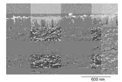
도 5는 본 발명의 개시내용의 이방성 나노구조 용품의 주사형 전자 현미경 사진이다.
<도 6>
도 6은 본 발명의 개시내용의 이방성 나노구조 용품의 주사형 전자 현미경 사진이다.
<도 7>
도 7은 본 발명의 개시내용의 일 방법에 따라 제조된 반사방지 층을 이용한, 디스플레이의 개략적인 단면도이다.<Figure 1>
1 is a first partial perspective view of a coating apparatus useful in the present disclosure.
<FIG. 2>
FIG. 2 is a second partial perspective view of the apparatus of FIG. 1 taken from another perspective. FIG.
3,
3 is a partial perspective view of another embodiment of a coating equipment removed from a gas containing chamber.
<Figure 4>
4 is a second perspective view of the apparatus of FIG. 3 taken from another perspective.
<Figure 5>
5 is a scanning electron micrograph of an anisotropic nanostructured article of the present disclosure.
6,
6 is a scanning electron micrograph of an anisotropic nanostructured article of the present disclosure.
<Figure 7>
7 is a schematic cross-sectional view of a display, using an antireflective layer made in accordance with one method of the present disclosure.
내용 중의 모든 숫자가 "약"이란 용어에 의해 어느 정도 변경되는 것으로 간주된다. 종점(endpoint)에 의한 숫자 범위의 상술(recitation)은 범위 내에 포함된 모든 숫자를 포함한다(예, 1 내지 5는 1, 1.5, 2, 2.75, 3, 3.80, 4 및 5). 내용 중에 언급된 모든 부분은 달리 지시되지 않으면, 중량 단위이다.All numbers in the text are considered to be somewhat altered by the term "about." The recitation of a range of numbers by endpoint includes all the numbers included in the range (eg 1 to 5 is 1, 1.5, 2, 2.75, 3, 3.80, 4 and 5). All parts mentioned in the text are by weight unless otherwise indicated.
나노구조 용품은 분산상을 가지는 매트릭스를 포함한다. 매트릭스(즉, 연속상)는 폴리머 물질, 액체 수지, 무기 물질, 또는 합금 또는 고체 용액(혼화성 폴리머 포함)을 포함할 수 있다.Nanostructured articles include a matrix having a dispersed phase. The matrix (ie, the continuous phase) may comprise a polymeric material, a liquid resin, an inorganic material, or an alloy or solid solution (including miscible polymers).
일 측면에서, 매트릭스는, 폴리카보네이트, 폴리(메트)아크릴레이트, 폴리에스테르, 나일론, 실록산, 플루오로폴리머, 우레탄, 에폭시, 환형 올레핀 코폴리머, 트라이아세테이트 셀룰로오스, 다이아크릴레이트 셀룰로오스 또는 이들의 블렌드 또는 코폴리머로 구성된 그룹으로부터 선택된 폴리머를 포함한다.In one aspect, the matrix is polycarbonate, poly (meth) acrylate, polyester, nylon, siloxane, fluoropolymer, urethane, epoxy, cyclic olefin copolymer, triacetate cellulose, diacrylate cellulose or blends thereof or And a polymer selected from the group consisting of copolymers.
유용한 폴리머 물질은 열가소성 및 열경화성 수지를 포함한다. 적합한 열가소성 물질은 폴리에틸렌 테레프탈레이트(PET), 폴리스티렌, 아클릴로니트릴 부타디엔 스티렌, 폴리비닐클로라이드, 염화 폴리비닐리덴, 폴리카보네이트, 폴리아크릴레이트, 열가소성 폴리우레탄, 폴리비닐 아세테이트, 폴리아미드, 폴리이미드, 폴리프로필렌, 폴리에스테르, 폴리에틸렌, 폴리(메틸메타크릴레이트), 폴리에틸렌 나프탈레이트, 스티렌 아크릴로니트릴, 실리콘-폴리옥사미드 폴리머, 플루오로폴리머, 사이클릭 올레핀 코폴리머, 열가소성 엘라스토머 등을 포함하나 이에 한정되지는 않는다.Useful polymeric materials include thermoplastic and thermosetting resins. Suitable thermoplastics include polyethylene terephthalate (PET), polystyrene, acrylonitrile butadiene styrene, polyvinylchloride, polyvinylidene chloride, polycarbonate, polyacrylate, thermoplastic polyurethane, polyvinyl acetate, polyamide, polyimide, poly Propylene, polyester, polyethylene, poly (methylmethacrylate), polyethylene naphthalate, styrene acrylonitrile, silicone-polyoxamide polymers, fluoropolymers, cyclic olefin copolymers, thermoplastic elastomers, and the like. Does not.
적합한 열경화성 수지는 아릴 수지 ((메트)아크릴레이트, 폴리에스테르 아크릴레이트, 우레탄 아크릴레이트, 에폭시 아크릴레이트 및 폴리에테르 아크릴레이트 포함), 에폭시, 열경화성 폴리우레탄, 실리콘 또는 폴리실록산 등을 포함하나, 이에 한정되지는 않는다. 이러한 수지는 대응하는 모노머 및/또는 올리고머를 포함하는 중합가능한 조성물의 반응 생성물로부터 형성될 수 있다.Suitable thermosetting resins include, but are not limited to, aryl resins (including (meth) acrylates, polyester acrylates, urethane acrylates, epoxy acrylates and polyether acrylates), epoxy, thermoset polyurethanes, silicones or polysiloxanes, and the like. Does not. Such resins may be formed from reaction products of polymerizable compositions comprising the corresponding monomers and / or oligomers.
일 실시예에서, 중합가능한 조성물은 적어도 하나의 모노머 또는 올리고머 (메트)아크릴레이트, 바람직하게는 우레탄 (메트)아크릴레이트를 포함한다. 전형적으로 모노머 또는 올리고머 (메트)아크릴레이트가 멀티(메트)아크릴레이트이다. "(메트)아크릴레이트"란 용어는 아크릴 및 메타크릴 산의 에스테르를 지칭하는 데 사용되고, 일반적으로 (메트)아크릴레이트 폴리머를 지칭하는 "폴리(메트)아크릴레이트"와 대조되게, "멀티(메트)아크릴레이트"는 하나 초과의 (메트)아크릴레이트 기를 함유하는 분자를 지칭한다. 가장 흔하게, 멀티(메트)아크릴레이트는 다이(메트)아크릴레이트이다. 그러나 또한, 트라이(메트)아크릴레이트, 테트라(메트)아크릴레이트 등을 이용하는 것이 고려된다.In one embodiment, the polymerizable composition comprises at least one monomer or oligomer (meth) acrylate, preferably urethane (meth) acrylate. Typically the monomer or oligomer (meth) acrylate is a multi (meth) acrylate. The term “(meth) acrylate” is used to refer to esters of acrylic and methacrylic acid, and in contrast to “poly (meth) acrylate”, which generally refers to (meth) acrylate polymers, refers to “multi (meth) ) Acrylate "refers to a molecule containing more than one (meth) acrylate group. Most often, the multi (meth) acrylate is a di (meth) acrylate. However, it is also contemplated to use tri (meth) acrylate, tetra (meth) acrylate and the like.
적합한 모노머 또는 올리고머 (메트)아크릴레이트는 알킬 (메트)아크릴레이트 (가령, 메틸 (메트)아크릴레이트, 에틸 (메트)아크릴레이트, 1-프로필 (메트)아크릴레이트 및 t-부틸 (메트)아크릴레이트)를 포함한다. 아크릴레이트는 (메트)아크릴 산의 (플루오로)알킬에스테르 모노머를 포함할 수 있으며, 모노머는 부분적으로 및/또는 완전히 플루오로화된, 가령 트라이플루오로에틸 (메트)아크릴레이트이다.Suitable monomers or oligomer (meth) acrylates are alkyl (meth) acrylates such as methyl (meth) acrylate, ethyl (meth) acrylate, 1-propyl (meth) acrylate and t-butyl (meth) acrylate ). The acrylate may comprise a (fluoro) alkylester monomer of (meth) acrylic acid, the monomer being partially and / or fully fluorinated, such as trifluoroethyl (meth) acrylate.
상업적으로 이용할 수 있는 멀티(메트)아크릴레이트 수지의 예는, 미츠비시 레이온 코., 엘티디의 DIABEAM 시리즈; 나가세 &컴퍼니, 엘티디.(Nagase & Company, Ltd.)의 DINACOL 시리즈; 신-나카무라 케미컬 코. 엘티디.의 NK ESTER 시리즈; 다이니폰 인크 & 케미컬스, 아이엔씨.(Dainippon Ink & Chemicals, Inc.)의 UNIDIC 시리즈, 토아고세 코. 엘티디.의 ARONIX 시리즈; NOF 코프.에 의해 제조된 BLENMER 시리즈; 니폰 카야쿠 코. 엘티디.의 KAYARAD 시리즈, 키오에이샤 케미컬 코. 엘티디의 LIGHT ESTER 시리즈 및 LIGHT ACRYLATE 시리즈를 포함한다.Examples of commercially available multi (meth) acrylate resins include, but are not limited to, Mitsubishi Rayon Co., Ltd., DIABEAM series; DINACOL series from Nagase & Company, Ltd .; Shin-Nakamura Chemical Nose. LT ESTER's NK ESTER series; Toagose Co., UNIDIC series by Dainippon Ink & Chemicals, Inc. Elti.'S ARONIX series; BLENMER series manufactured by NOF Corp .; Nippon Kayaku Ko. L.D.KAYARAD series, Kioisha chemical nose. Includes LTI's LIGHT ESTER series and LIGHT ACRYLATE series.
올리고머 우레탄 멀티(메트)아크릴레이트는, 예를 들면 사토머로부터, 상표명 "Photomer 6000 시리즈"(가령 "Photomer 6010" 및 "Photomer 6020"), 그리고 또한 상표명 "CN 900 시리즈"(가령 "CN966B85", "CN964" 및 "CN972")로 상업적으로 입수할 수 있다. 올리고머 우레탄 (메트)아크릴레이트는 또한 서피스 스페셜티스(Surface Specialties)로부터, 가령 상표명 "Ebecryl 8402", "Ebecryl 8807" 및 "Ebecryl 4827"으로 입수할 수 있다. 올리고머 우레탄 (메트)아크릴레이트는 또한 폴리올과, 화학식 OCN-R3-NCO의 알킬렌 또는 방향족 다이아이소시아네이트의 초기 반응에 의해 제조될 수 있다. 가장 흔하게, 폴리올은 화학식 HO-R4-OH의 다이올이며, 여기서, R3는 C2-100 알킬렌 또는 아릴렌 기이고 R4는 C2-100 알킬렌 기이다. 이어서 중간 생성물은 우레탄 다이올 다이아이소시아네이트이며, 이는 후속으로 하이드록시알킬 (메트)아크릴레이트와의 반응을 거칠 수 있다. 적합한 다이아이소시아네이트는 2,2,4-트라이메틸헥실렌 다이아이소시아네이트 및 톨루엔 다이아이소시아네이트를 포함한다. 알킬렌 다이아이소시아네이트가 일반적으로 바람직하다. 특히 바람직한 이러한 유형의 화합물은 2,2,4-트라이메틸헥실렌 다이아이소시아네이트, 폴리(카프로락톤)다이올 및 2-하이드록시에틸 메타크릴레이트로부터 제조될 수 있다. 적어도 일부의 경우에, 우레탄 (메트)아크릴레이트는 지방족 화합물인 것이 바람직하다.Oligomeric urethane multi (meth) acrylates are available, for example, from Satomer under the trade names "Photomer 6000 series" (such as "Photomer 6010" and "Photomer 6020"), and also under the trade names "CN 900 series" (such as "CN966B85", "CN964" and "CN972") are commercially available. Oligomeric urethane (meth) acrylates are also available from Surface Specialties, for example under the trade names "Ebecryl 8402", "Ebecryl 8807" and "Ebecryl 4827". Oligomeric urethane (meth) acrylates can also be prepared by initial reaction of polyols with alkylene or aromatic diisocyanates of the formula OCN-R 3 -NCO. Most often, the polyol is a diol of the formula HO-R 4 -OH, wherein R 3 is a C2-100 alkylene or arylene group and R 4 is a C2-100 alkylene group. The intermediate product is then urethane diol diisocyanate, which may subsequently be reacted with hydroxyalkyl (meth) acrylate. Suitable diisocyanates include 2,2,4-trimethylhexylene diisocyanate and toluene diisocyanate. Alkylene diisocyanates are generally preferred. Particularly preferred compounds of this type can be prepared from 2,2,4-trimethylhexylene diisocyanate, poly (caprolactone) diol and 2-hydroxyethyl methacrylate. In at least some cases, the urethane (meth) acrylate is preferably an aliphatic compound.
중합가능한 조성물은 다양한 모노머 및/또는 올리고머의 혼합물일 수 있으며, 동일한 또는 다른 반응성 작용기를 가진다. 둘 이상의 다른 작용기를 포함하는 중합가능한 조성물이 사용될 수 있고, 다음을 포함한다; (메트)아크릴레이트, 에폭시 및 우레탄. 다른 작용기가 다른 모노머 및/또는 올리고머 모이어티에 또는 동일한 모노머 및/또는 올리고머 모이어티에 함유될 수 있다. 예를 들어, 수지 조성물은 곁사슬에 에폭시 기 및/또는 하이드록실 기를 가지는 아크릴 또는 우레탄 수지, 아미노 기를 가지는 화합물, 및 선택적으로 분자 내에 에폭시 기 또는 아미노 기를 가지는 실란 화합물을 포함할 수 있다.The polymerizable composition may be a mixture of various monomers and / or oligomers and have the same or different reactive functionalities. Polymerizable compositions comprising two or more different functional groups can be used and include: (Meth) acrylates, epoxies and urethanes. Different functional groups may be contained in different monomers and / or oligomer moieties or in the same monomers and / or oligomer moieties. For example, the resin composition may comprise an acrylic or urethane resin having an epoxy group and / or a hydroxyl group in the side chain, a compound having an amino group, and optionally a silane compound having an epoxy group or an amino group in the molecule.
열경화성 수지 조성물은 열 경화, 광경화(화학선 복사에 의한 경화) 및/또는 e-빔 경화와 같은 통상적인 기술을 사용하여 중합화 가능하다. 일 실시예에서, 수지는 자외선(UV) 및/또는 가시광에 수지를 노출함으로써 광중합화된다. 통상적인 경화제(curative) 및/또는 촉매가 중합가능한 조성물에 사용될 수 있고, 조성물 내의 작용기(들)에 근거하여 선택될 수 있다. 여러 경화제 및/또는 촉매는 여러 경화 기능기가 사용되는 경우에, 필요할 수 있다. 하나 이상의 경화 기술(가령, 열 경화, 광경화 및 e-빔 경화)를 조합하는 것은 본 개시내용의 범위 내이다.The thermosetting resin composition is polymerizable using conventional techniques such as thermosetting, photocuring (curing by actinic radiation) and / or e-beam curing. In one embodiment, the resin is photopolymerized by exposing the resin to ultraviolet (UV) and / or visible light. Conventional curatives and / or catalysts may be used in the polymerizable composition and may be selected based on the functional group (s) in the composition. Several curing agents and / or catalysts may be necessary when several curing functionalities are used. Combining one or more curing techniques (eg, thermal curing, photocuring and e-beam curing) is within the scope of the present disclosure.
나아가, 중합가능한 수지가 적어도 하나의 다른 모노머 및/또는 올리고머(전술한 것과 이외의 것, 즉 모노머 또는 올리고머 (메트)아크릴레이트 및 올리고머 우레탄 (메트)아크릴레이트)를 포함하는 조성물일 수 있다. 이러한 다른 모노머는 점도 감소 및/또는 열화학적 속성 개선 및/또는 굴절률 증가를 일으킬 수 있다. 이러한 속성을 가지는 모노머는 아크릴 모노머(즉, 아크릴레이트 및 메타크릴레이트 에스테르, 아크릴아미드 및 메타크릴아미드), 스티렌 모노머 및 에틸렌형 불포화 니트로겐 헤테로사이클을 포함한다.Furthermore, the polymerizable resin may be a composition comprising at least one other monomer and / or oligomer (other than those described above, ie monomer or oligomer (meth) acrylate and oligomeric urethane (meth) acrylate). Such other monomers can lead to reduced viscosity and / or improved thermochemical properties and / or increased refractive index. Monomers having this property include acrylic monomers (ie acrylate and methacrylate esters, acrylamides and methacrylamides), styrene monomers and ethylenically unsaturated nitrogen heterocycles.
또한 다른 기능성을 가지는 (메트)아크릴레이트 에스테르가 포함된다. 이러한 유형의 화합물은 2-(N-부틸카바밀)에틸 (메트)아크릴레이트, 2,4-다이클로로페닐 아크릴레이트, 2,4,6-트라이브로모페닐 아크릴레이트, 트라이브로모페녹실에틸 아크릴레이트, t-부틸페닐 아크릴레이트, 페닐 아크릴레이트, 페닐 티오아크릴레이트, 페닐티오에틸 아크릴레이트, 알콕시레이티드 페닐 아크릴레이트, 아이소보르닐 아크릴레이트 및 페녹시에틸 아크릴레이트에 의해 예시된다. 또한, 테트라브로모비스페놀 A 다이에폭사이드 및 (메트)아크릴산의 반응 생성물이 적합하다.Also included are (meth) acrylate esters having other functionality. Compounds of this type are 2- (N-butylcarbamyl) ethyl (meth) acrylate, 2,4-dichlorophenyl acrylate, 2,4,6-tribromophenyl acrylate, tribromophenoxylethyl acrylate , t-butylphenyl acrylate, phenyl acrylate, phenyl thioacrylate, phenylthioethyl acrylate, alkoxylated phenyl acrylate, isobornyl acrylate and phenoxyethyl acrylate. Also suitable are reaction products of tetrabromobisphenol A diepoxide and (meth) acrylic acid.
또한, 다른 모노머는 모노머의 N-치환된 또는 N,N-이치환된 (메트)아크릴아미드, 특히 아크릴아미드일 수 있다. 이들은 N-알킬아크릴아미드 및 N,N-다이알킬아크릴아미드, 특히 -4알킬 기를 포함하는 것을 포함한다. 예는 N-아이소프로필아크릴아미드, N-t-부틸아크릴아미드, N,N-다이메틸아크릴아미드 및 N,N-다이에틸아크릴아미드이다.Other monomers may also be N-substituted or N, N-disubstituted (meth) acrylamides, in particular acrylamides. These include N-alkylacrylamides and N, N-dialkylacrylamides, especially those containing -4 alkyl groups. Examples are N-isopropylacrylamide, N-t-butylacrylamide, N, N-dimethylacrylamide and N, N-diethylacrylamide.
다른 모노머는 추가로 폴리올 멀티(메트)아크릴레이트일 수 있다. 이러한 화합물은 2-10 탄소 원자를 함유하는 지방족 다이올, 트라이올, 및/또는 테트라올로부터 제조되는 것이 일반적이다. 적합한 폴리(메트)아크릴레이트의 예는, 에틸렌 글리콜 다이아크릴레이트, 1,6-헥산다이올 다이아크릴레이트, 2-에틸-2-하이드록시메틸-1,3-프로판다이올 트라이아실레이트 (트라이메틸올프로판 트라이 아크릴레이트), 다이(트라이메틸올프로판) 테트라아크릴레이트, 펜타에리스리톨 테트라아크릴레이트, 대응하는 메타크릴레이트 및 상기 폴리올의 알콕시레이티드 (보통 에톡시레이티드) 유도체의 (메트)아크릴레이트이다. 둘 이상의 에틸렌형 불포화 그룹을 가지는 모노머가 크로스링커로서 기능을 할 수 있다.The other monomer may further be a polyol multi (meth) acrylate. Such compounds are generally prepared from aliphatic diols, triols, and / or tetraols containing 2-10 carbon atoms. Examples of suitable poly (meth) acrylates include ethylene glycol diacrylate, 1,6-hexanediol diacrylate, 2-ethyl-2-hydroxymethyl-1,3-propanediol triacylate (tri Methylolpropane triacrylate), di (trimethylolpropane) tetraacrylate, pentaerythritol tetraacrylate, corresponding methacrylates and (meth) acrylates of alkoxylated (usually ethoxylated) derivatives of the polyols Rate. Monomers having two or more ethylenically unsaturated groups can function as crosslinkers.
다른 모노머로서 사용하기에 적합한 스티렌 화합물은 스티렌, 다이클로로스티렌, 2,4,6-트라이클로로스티렌, 2,4,6-트라이브로모스티렌, 4-메틸스티렌 및 4-페녹시스티렌을 포함한다. 에틸렌형 불포화 니트로겐 헤테로사이클은 N-비닐피롤리돈 및 비닐피리딘을 포함한다.Styrene compounds suitable for use as other monomers include styrene, dichlorostyrene, 2,4,6-trichlorostyrene, 2,4,6-tribromostyrene, 4-methylstyrene and 4-phenoxystyrene. Ethylenically unsaturated nitrogen heterocycles include N-vinylpyrrolidone and vinylpyridine.
복사선 경화성 물질 내의 성분 비율이 변경될 수 있다. 일반적으로, 유기 성분은 약 30-100% 모노머 및/또는 올리고머 (메트)아크릴레이트 또는 올리고머 우레탄 멀티(메트)아크릴레이트를 포함할 수 있으며, 여기서 다른 모노머 및/또는 올리고머와 임의의 균형이 이루어진다.The proportion of components in the radiation curable material may vary. In general, the organic component may comprise about 30-100% monomer and / or oligomer (meth) acrylate or oligomeric urethane multi (meth) acrylate, where any balance is made with other monomers and / or oligomers.
상업적으로 입수할 수 있는 액체-수지 기반 물질(일반적으로, "하드코트"라 함)이 매트릭스로 또는 매트릭스의 성분으로 사용될 수 있다. 이러한 물질은 캘리포니아 하드코팅 코.(샌 디에고, 캘리포니아)의 PERMANEW 시리즈 및 모멘티브 퍼포먼트 머티리얼(알바니, 뉴욕)의 UVHC 시리즈 하드코트를 포함한다. 추가로, 상업적으로 입수할 수 있는 나노입자 채움 매트릭스(nanoparticle filled matrix)가 나노레진스 아게(기스타흐트, 독일)의 NANOCRYL 및 NANOPOX와 같이 사용될 수 있다.Commercially available liquid-resin based materials (commonly referred to as "hardcoats") can be used as the matrix or as a component of the matrix. Such materials include the PERMANEW series from California Hard Coatings Co. (San Diego, CA) and the UVHC series hard coat from Momentive Performance Materials (Albany, NY). In addition, commercially available nanoparticle filled matrices can be used, such as NANOCRYL and NANOPOX of NanoResin AG (Gistach, Germany).
추가적으로, 나노미립자 함유 하드코트 필름, 가령 토레이 어드벤스드 필름스 코. 엘티디.(도쿄, 일본)의 THS 시리즈; 린텍 코프.(도쿄, 일본)의 FPD 용 Opteria 하드코팅 필름; 소니 케미컬 디바이스 코프.(도쿄, 일본)의 Sony 광학 필름; SKC 하스(서울, 한국)의 하드코팅 필름 및 테크라 코프.(밀워키, 위스콘신)의 테라핀 G 필름이 매트릭스 또는 매트릭스의 성분으로 사용될 수 있다.Additionally, nanoparticulate containing hardcoat films such as Toray Advanced Films Co. THS series of Elti. (Tokyo, Japan); Opteria hard coating film for FPD of Lintec Corp. (Tokyo, Japan); Sony optical film from Sony Chemical Devices Corp. (Tokyo, Japan); Hard coating films of SKC Haas (Seoul, Korea) and terrapine G films of Techla Corp. (Milwaukee, Wisconsin) may be used as the matrix or components of the matrix.
표면 레벨링 제가 매트릭스에 부가될 수 있다. 바람직하게 레벨링 제는 매트릭스 수지를 평탄화(smoothing)하기 위해 사용된다. 예는, 실리콘-레벨링 제, 아크릴-레벨링 제 및 플루오린-함유-레벨링 제를 포함한다. 일 실시예에서, 실리콘-레벨링 제는 폴리다이메틸 실록산 백본(여기에 폴리옥시알킬렌 기가 부가됨)을 포함한다.Surface leveling agents can be added to the matrix. Preferably the leveling agent is used to smooth the matrix resin. Examples include silicon-leveling agents, acrylic-leveling agents and fluorine-containing-leveling agents. In one embodiment, the silicon-leveling agent comprises a polydimethyl siloxane backbone, to which a polyoxyalkylene group is added.
매트릭스에 유용한 무기물은 예를 들면, 유리, 금속, 금속 옥사이드 및 세라믹을 포함한다. 바람직한 무기물은 규소 옥사이드, 지르코니아, 바나듐 펜트옥사이드 및 텅스텐 카바이드를 포함한다.Minerals useful in the matrix include, for example, glass, metals, metal oxides and ceramics. Preferred inorganics include silicon oxide, zirconia, vanadium pentoxide and tungsten carbide.
나노스케일 분산상은 매트릭스 내에 무작위적으로 분산된 불연속상이다. 나노스케일 분산상은 나노입자(예를 들면, 나노스피어), 나노튜브, 나노섬유, 케이지 분자, 하이퍼브랜치 분자, 미셀(micelles), 리버스 미셀 등을 포함할 수 있다. 바람직하게, 분산상은 나노입자 또는 케이지 분자를 포함하고; 더 바람직하게는 분산상이 나노입자를 포함한다.Nanoscale dispersed phases are discrete phases randomly dispersed within the matrix. Nanoscale dispersed phases may include nanoparticles (eg, nanospheres), nanotubes, nanofibers, cage molecules, hyperbranched molecules, micelles, micelles, reverse micelles, and the like. Preferably, the dispersed phase comprises nanoparticles or cage molecules; More preferably the dispersed phase comprises nanoparticles.
나노입자는 바람직하게 약 1 nm 내지 약 100 nm 범위의 평균 지름을 가진다. 바람직하게, 나노입자는 5 nm, 20 nm, 또는 80 nm의 평균 지름을 가진다. 분산상을 위한 나노입자가 금속, 금속 옥사이드, 카바이드, 나이트라이드, 보라이드, 할라이드, 플루오로카본 고체 등, 또는 이들의 혼합물을 포함할 수 있다. 바람직한 물질은 SiO2, ZrO2, TiO2, ZnO, 칼슘 카보네이트, 마그네슘 실리케이트, 인듐 틴 옥사이드, 안티모니 틴 옥사이드, 카본, 폴리(테트라플루오로에틸렌) 등을 포함한다. 바람직하게는, 나노입자가 SiO2를 포함한다.Nanoparticles preferably have an average diameter in the range from about 1 nm to about 100 nm. Preferably, the nanoparticles have an average diameter of 5 nm, 20 nm, or 80 nm. Nanoparticles for the dispersed phase can include metals, metal oxides, carbides, nitrides, borides, halides, fluorocarbon solids, and the like, or mixtures thereof. Preferred materials include SiO 2 , ZrO 2 , TiO 2 , ZnO, calcium carbonate, magnesium silicate, indium tin oxide, antimony tin oxide, carbon, poly (tetrafluoroethylene), and the like. Preferably, the nanoparticles comprise SiO 2 .
나노입자는 매트릭스에 약 1 중량% 내지 약 60중량%, 또는 약 10 중량% 내지 약 40 중량%의 양으로 매트릭스 내에 존재할 수 있다. 본 발명의 개시내용의 물질에서 사용하기 위한 실리카는 날코 케미컬 코.(나퍼빌, 일리노이)로부터, 상표명 "Nalco Colloidal Silicas"(가령, 제품 1040, 1042, 1050, 1060, 2327 및 2329)로, 상업적으로 입수할 수 있다. 적합한 건식 실리카는, 예를 들면 에보닉으로부터, 상표명, "Aerosil 시리즈 OX-50", 및 제품 번호 -130, -150, 및 -200로 상업적으로 입수할 수 있는 제품을 포함한다. 또한, 다른 콜로이드 실리카는 니산 케미컬스로부터 상표명 "IPA-ST", "IPA-ST-L", 및 "IPA-ST-ML"으로 입수할 수 있다. 건식 실리카는 또한, 카보트 코프.(투스콜라, 일리노이)로부터, 상표명 "CAB-O-SPERSE 2095", "CAB-O-SPERSE A105", 및 "CAB-O-SIL M5"으로 상업적으로 입수할 수 있다. 조성물에서 사용하기 위한 지르코니아 및 본 발명의 용품은 날코 케미컬 코.로부터 상표명 "Nalco OOSSOO8"로 입수할 수 있다.Nanoparticles may be present in the matrix in an amount of about 1% to about 60%, or about 10% to about 40% by weight in the matrix. Silicas for use in the materials of the present disclosure are commercially available from Nalco Chemical Co. (Napperville, Illinois) under the trade name “Nalco Colloidal Silicas” (eg, products 1040, 1042, 1050, 1060, 2327 and 2329). You can get it. Suitable dry silicas include, for example, products available from Evonik under the trade names "Aerosil Series OX-50", and product numbers -130, -150, and -200. Other colloidal silicas are also available from Nissan Chemicals under the trade names "IPA-ST", "IPA-ST-L", and "IPA-ST-ML". Dry silica is also commercially available from Cabot Corp. (Tuscola, Illinois) under the trade names "CAB-O-SPERSE 2095", "CAB-O-SPERSE A105", and "CAB-O-SIL M5". Can be. Zirconia and articles of the invention for use in the composition are available under the trade name "Nalco OOSSOO8" from Nalco Chemical Co.
나노-크기 입자를 표면-처리하면 폴리머 수지 중 안정한 분산물을 제공할 수 있다. 바람직하게, 입자가 중합 가능한 수지 내에 잘 분산될 것이고, 실질적으로 균질한 조성물이 얻어지도록 표면-처리가 나노입자를 안정화한다. 나아가, 안정화된 입자가 경화 중에 중합 가능한 수지와 공중합화 또는 반응을 할 수 있도록 나노입자가 표면 처리제로 표면의 적어도 일부 상부에서 개질될 수 있다.Surface-treating the nano-sized particles can provide a stable dispersion in the polymer resin. Preferably, the particles will be well dispersed in the polymerizable resin and the surface-treatment stabilizes the nanoparticles so that a substantially homogeneous composition is obtained. Furthermore, nanoparticles can be modified on at least a portion of the surface with a surface treating agent so that the stabilized particles can copolymerize or react with the polymerizable resin during curing.
바람직하게 나노입자는 표면처리제로 처리된다. 일반적으로, 표면 처리제는 입자 표면에 (공유적으로, 이온적으로 또는 강한 물리흡착을 통해) 부착될 제1 말단 및 입자와 수지와의 상용성을 부여하고/하거나 경화 동안 수지와 반응하는 제2 말단을 갖는다. 표면 처리제의 예에는 알코올, 아민, 카르복실산, 설폰산, 포스폰산, 실란 및 티탄산염이 포함된다. 바람직한 유형의 처리제는, 금속 산화물 표면의 화학적 성질에 의해서 부분적으로 결정된다. 실란이 실리카에 바람직하고 규산질 충전제에는 다른 것이 바람직하다. 실란 및 카르복실산이 지르코니아와 같은 금속 산화물에 바람직하다. 표면 개질은 단량체들과의 혼합에 대하여 후속적으로 또는 혼합 후에 행해질 수 있다. 실란의 경우에, 수지 내로 혼입하기 전에, 실란이 입자 또는 나노입자 표면과 반응하는 것이 바람직하다. 표면 개질제의 바람직한 양은 입자 크기, 입자 유형, 개질제의 분자량 및 개질제 유형과 같은 수 개의 요인에 따라 달라진다.Preferably the nanoparticles are treated with a surface treating agent. In general, the surface treating agent is a first end to be attached (covalently, ionically or via strong physisorption) to the particle surface and a second to impart compatibility of the particle with the resin and / or react with the resin during curing. Have ends. Examples of surface treatment agents include alcohols, amines, carboxylic acids, sulfonic acids, phosphonic acids, silanes and titanates. Preferred types of treatment agents are determined in part by the chemical nature of the metal oxide surface. Silanes are preferred for silica and others for siliceous fillers. Silanes and carboxylic acids are preferred for metal oxides such as zirconia. Surface modification can be done subsequently or after mixing with the monomers. In the case of silane, it is preferred that the silane reacts with the particle or nanoparticle surface prior to incorporation into the resin. The preferred amount of surface modifier depends on several factors, such as particle size, particle type, molecular weight of the modifier and type of modifier.
표면 처리제의 대표적인 실시예는 예를 들면, 아이소옥틸 트라이-메톡시-실란, N-(3-트라이에톡시릴프로필)메톡시에톡시-에톡시에틸 카바메이트(PEG3TES), N-(3-트라이에톡시릴프로필)메톡시에톡시에톡시에틸 카바메이트(PEG2TES), 3-(메타크릴로일옥시)프로필트라이메톡시실란, 3-아크릴옥시프로필트라이메톡시실란, 3-(메타크릴로일옥시)프로필트라이에톡시실란, 3-(메타크릴로일옥시)프로필메틸다이메톡시실란, 3-(아크릴로일록시프로필)메틸다이메톡시실란, 3-(메타크릴로일옥시)프로필다이메틸에톡시실란, 비닐다이메틸에톡시실란, 페닐트라이메타옥시실란, n-옥틸트라이메톡시실란, 도데실트라이메톡시실란, 옥타데실트라이메톡시실란, 프로필트라이메톡시실란, 헥실트라이메톡시실란, 비닐메틸다이악톡시실란, 비닐메틸다이에톡시실란, 비닐트라이아세톡시실란, 비닐트라이에톡시실란, 비닐트라이아이소프로폭시실란, 비닐트라이메톡시실란, 비닐트라이페녹시실란, 비닐트라이-t-부톡시실란, 비닐트라이-아이소부톡시실란, 비닐트라이아이소프로페녹시실란, 비닐트라이s(2-메톡시에톡시)실란, 스티릴에틸트라이메톡시실란, 메르캅토프로필트라이메톡시실란, 3-글리시독시프로필트라이메톡시실란, 아크릴산, 메타크릴산, 올레산, 스테아릭산, 도데칸산, 2-(2-(2-메톡시에톡시)에톡시)아세트산(MEEAA), 베타-카르복시에틸아크릴레이트, 2-(2-메톡시에톡시)아세트산, 메톡시페닐 아세트산, 및 이들의 혼합물과 같은 화합물을 포함한다. 나아가, 또한, OSI 스페셜티스(크롬프턴 사우스 찰스턴, 웨스트버지니아)로부터 상표명 "Silquest A1230"으로 입수할 수 있는 독점적(proprietary) 실란 표면 개질제가 적합할 수 있다.Representative examples of surface treatment agents are, for example, isooctyl tri-methoxy-silane, N- (3-triethoxyylpropyl) methoxyethoxy-ethoxyethyl carbamate (PEG3TES), N- (3 -Triethoxyylpropyl) methoxyethoxyethoxyethyl carbamate (PEG2TES), 3- (methacryloyloxy) propyltrimethoxysilane, 3-acryloxypropyltrimethoxysilane, 3- (methacryl Royloxy) propyltriethoxysilane, 3- (methacryloyloxy) propylmethyldimethoxysilane, 3- (acryloyloxypropyl) methyldimethoxysilane, 3- (methacryloyloxy) Propyldimethylethoxysilane, vinyldimethylethoxysilane, phenyltrimethoxysilane, n-octyltrimethoxysilane, dodecyltrimethoxysilane, octadecyltrimethoxysilane, propyltrimethoxysilane, hexyl Trimethoxysilane, VinylmethylDiacoxysilane, Vinylmethyldiethoxysilane, Vinyl Tri Acetoxysilane, vinyltriethoxysilane, vinyltriisopropoxysilane, vinyltrimethoxysilane, vinyltriphenoxysilane, vinyltri-t-butoxysilane, vinyltri-isobutoxysilane, vinyltriisopro Phenoxysilane, vinyltris (2-methoxyethoxy) silane, styrylethyltrimethoxysilane, mercaptopropyltrimethoxysilane, 3-glycidoxypropyltrimethoxysilane, acrylic acid, methacrylic acid, Oleic acid, stearic acid, dodecanoic acid, 2- (2- (2-methoxyethoxy) ethoxy) acetic acid (MEEAA), beta-carboxyethylacrylate, 2- (2-methoxyethoxy) acetic acid, methoxy Compounds such as phenyl acetic acid, and mixtures thereof. Furthermore, proprietary silane surface modifiers, available under the trade designation “Silquest A1230” from OSI Specialties (Cromtonton South Charleston, WV), may be suitable.
콜로이드 분산물 내의 입자의 표면 개질은 다양한 방식으로 이루어질 수 있다. 프로세스는 표면 개질제와 무기 분산물의 혼합물을 포함한다. 선택적으로, 공용매는 예를 들면, 1-메톡시-2-프로판올, 에탄올, 아이소프로판올, 에틸렌 글리콜, N,N-다이메틸아세트아미드 및 1-메틸-2-피롤리딘온과 같이, 이 시점에서 첨가될 수 있다. 공용매는 표면 개질제뿐만 아니라 표면 개질된 입자의 용해성을 향상시킬 수 있다. 무기 졸 및 표면 개질제를 포함하는 혼합물은 실온 또는 승온에서, 혼합하거나 혼합하지 않으면서 후속적으로 반응시킨다. 일 방법에서, 혼합물이 약 24시간 동안 약 85℃에서 반응될 수 있고, 표면 개질된 졸(sol)이 생성된다. 다른 방법에서, 금속 옥사이드가 표면 개질되는 경우에, 금속 옥사이드의 표면 처리는 입자 표면으로의 산성분자의 흡착을 포함하는 것이 바람직할 수 있다. 중금속 옥사이드의 표면 개질은 실내 온도에서 이루어지는 것이 바람직하다.Surface modification of the particles in the colloidal dispersion can be accomplished in a variety of ways. The process includes a mixture of surface modifiers and inorganic dispersions. Optionally, the cosolvent may be at this point, for example 1-methoxy-2-propanol, ethanol, isopropanol, ethylene glycol, N, N-dimethylacetamide and 1-methyl-2-pyrrolidinone Can be added. Cosolvents can improve the solubility of surface modified particles as well as surface modifiers. The mixture comprising the inorganic sol and the surface modifier is subsequently reacted at room or elevated temperature, with or without mixing. In one method, the mixture can be reacted at about 85 ° C. for about 24 hours, resulting in a surface modified sol. In another method, where the metal oxide is surface modified, it may be desirable for the surface treatment of the metal oxide to include adsorption of acid components onto the particle surface. Surface modification of heavy metal oxides is preferably carried out at room temperature.
실란을 이용한 ZrO2의 표면 개질은 산성 조건 또는 염기성 조건 하에서 이루어질 수 있다. 하나의 경우에, 실란이 적합한 시간 구간 동안 산성 조건하에서 가열된다. 이때, 이 분산액이 수성 암모니아(또는 다른 염기)와 조합된다. 이러한 방법은 ZrO2 표면으로부터의 산 반대 이온의 제거뿐만 아니라 실란과의 반응을 가능하게 한다. 다른 방법에서, 입자는 분산물로부터 침전되고 액상으로부터 분리된다.Surface modification of ZrO 2 with silanes can be made under acidic or basic conditions. In one case, the silane is heated under acidic conditions for a suitable time period. This dispersion is then combined with aqueous ammonia (or other base). This method enables the reaction with silane as well as the removal of acid counter ions from the ZrO 2 surface. In another method, particles precipitate from the dispersion and separate from the liquid phase.
표면 개질제들의 조합이 유용할 수 있으며, 여기서, 적어도 하나의 표면 개질제는 경화성 수지와 공중합성인 작용기를 갖는다. 예를 들어, 중합 기는 에틸렌계 불포화 작용기 또는 개환 중합되는 환형 작용기일 수 있다. 에틸렌계 불포화 중합 기는, 예를 들어, 아크릴레이트 또는 메타크릴레이트 또는 비닐 기일 수 있다. 개환 중합되는 환형 작용기는 일반적으로 산소, 황 또는 질소와 같은 헤테로원자를 포함하며, 바람직하게는 에폭사이드와 같이 산소를 함유하는 3원 고리를 포함한다.Combinations of surface modifiers may be useful, where at least one surface modifier has a functional group copolymerizable with the curable resin. For example, the polymerization group may be an ethylenically unsaturated functional group or a cyclic functional group which is ring-opened polymerized. The ethylenically unsaturated polymerizable group can be, for example, an acrylate or methacrylate or vinyl group. The cyclic functional groups to be ring-opened polymerized generally comprise heteroatoms such as oxygen, sulfur or nitrogen, and preferably comprise three-membered rings containing oxygen such as epoxides.
나노분산상에 대한 유용한 케이지 분자는 다면체 올리고머 실세스퀴옥산 분자를 포함하며, 이는 실리콘 및 산소의 케이지-형 하이브리드 분자이다. 다면체 올리고머 실세스퀴옥산(POSS) 분자가 합성물 및 명칭의 공유 시스템 양자를 통해 실리콘에 밀접하게 관련된 성분의 지속적으로 발달하는 클래스로부터 유래된다. POSS 분자는 다음의 두 개의 고유 특징을 가진다: (1) 화학적 조성물이 실리카(SiO2) 및 실리콘(R2SiO) 사이의 하이브리드, 중간생성물(RSiO1.5)이고, (2) 분자는 폴리머 치수에 비해 물리적으로 크며, 대부분의 폴리머 세그먼트 및 코일과 사이즈 면에서 거의 동일하다. 결과적으로, POSS 분자는 실리카의 최소 입자(약 1- 1.5 nm)만큼 작은 것으로 생각될 수 있다. 그러나, 실리카 또는 개질된 점토와 달리, 각각의 POSS 분자는 중합에 적합한 또는 폴리머 체인에 POSS 모노머를 접합하기에 적합한 공유 결합된 반응성 기능기를 함유한다. 또한, POSS 아크릴레이트 및 메타크릴레이트 모노머가 자외선(UV) 경화에 적합하다. 고 기능성 POSS 아크릴레이트 및 메타크릴레이트(예를 들면, MA0735 및 MA0736)가 기계적으로 내구력이 있는 하드코트를 형성하기 위해 대부분의 UV-경화성 아크릴 및 우레탄 아크릴 모노머 또는 올리고머와 혼화 가능하다. 하드코트에서 POSS 분자는 유기 코팅 매트릭스 내에 균일하게 분산된 나노-상을 형성한다.Useful cage molecules for the nanodisperse phase include polyhedral oligomeric silsesquioxane molecules, which are cage-type hybrid molecules of silicon and oxygen. Polyhedral oligomeric silsesquioxane (POSS) molecules are derived from a constantly evolving class of components that are closely related to silicon through both the composite and the covalent system of designation. POSS molecules have two unique characteristics: (1) the chemical composition is a hybrid, intermediate (RSiO 1.5 ) between silica (SiO 2 ) and silicon (R 2 SiO), and (2) the molecule It is physically large in size and is almost identical in size to most polymer segments and coils. As a result, the POSS molecules can be thought of as small as the smallest particles of silica (about 1-1.5 nm). However, unlike silica or modified clays, each POSS molecule contains covalently bonded reactive functional groups suitable for polymerization or for bonding POSS monomers to polymer chains. In addition, POSS acrylate and methacrylate monomers are suitable for ultraviolet (UV) curing. Highly functional POSS acrylates and methacrylates (eg, MA0735 and MA0736) are miscible with most UV-curable acrylic and urethane acrylic monomers or oligomers to form mechanically durable hardcoats. POSS molecules in the hardcoat form nano-phases uniformly dispersed within the organic coating matrix.
또한 탄소는 미국 특허 제7,368,161호(맥그루앙 등)에서와 같이 그래파이트, 카본 나노튜브, 벌키 볼, 또는 카본 블랙의 형태로 나노분산상에서 사용될 수 있다.Carbon may also be used in the nanodispersed phase in the form of graphite, carbon nanotubes, bulky balls, or carbon black, as in US Pat. No. 7,368,161 (McGruang et al.).
나노분산상에서 사용될 수 있는 추가적인 물질은 Irgastat™ P18(시바 코포레이션(테리타운, 뉴욕)에서 입수할 수 있음)를 포함하며, 암파세트(Ampacet) LR-92967(암파세트 코포레이션(테리타운, 뉴욕)에서 입수할 수 있음)을 포함한다.Additional materials that can be used in the nanodispersed phase include Irgastat ™ P18 (available from Ciba Corporation (Terrytown, NY)), and from Amphaset LR-92967 (Ampacet Corporation (Terrytown, NY) Available).
일반적으로 분산상은 약 1 중량 % 내지 약 50 중량 %; 바람직하게는 약 5 중량 % 내지 약 25 중량 %의 농도로 매트릭스에 존재한다.Generally, the dispersed phase is about 1% to about 50% by weight; Preferably at a concentration of about 5% to about 25% by weight.
본 발명의 나노구조 용품은 나노구조 이방성 표면을 가진다. 일반적으로 나노구조 이방성 표면은 약 2:1 이상의; 바람직하게는 약 5:1 이상의 높이 대 폭 비율을 가지는 나노형상물을 포함한다. 일부 실시예에서, 높이 대 폭 비율은 심지어 50:1 이상이고, 100:1 이상이거나, 200:1 이상이다. 나노구조 이방성 표면은, 예를 들면, 나노-필러 또는 나노-컬럼과 같은 나노형상물, 또는 연속적인 나노-벽(나노-필러 또는 나노-컬럼 포함)을 포함할 수 있다. 바람직하게는, 나노형상물이 기판에 대략적으로 수직인 가파른 측벽을 가진다. 일부 실시예에서, 나노형상물의 대부분이 분산상 물질로 캡핑된다(capped). 표면에서의 분산상의 농도(매트릭스의 내부에서에 관하여)가 약 5 중량% 내지 약 90 중량%일 수 있고; 바람직하게는 약 10 중량 % 내지 75 중량 %일 수 있다. 일부 실시예에서, 분산상의 농도가 매트릭스 내에서 보다 매트릭스의 표면에서 더 높다.Nanostructured articles of the invention have nanostructured anisotropic surfaces. Generally, the nanostructured anisotropic surface is at least about 2: 1; Preferably, the nanostructures have a height to width ratio of about 5: 1 or more. In some embodiments, the height to width ratio is even 50: 1 or more, 100: 1 or more, or 200: 1 or more. Nanostructured anisotropic surfaces can include, for example, nanoforms such as nano-fillers or nano-columns, or continuous nano-walls (including nano-fillers or nano-columns). Preferably, the nanostructures have steep sidewalls that are approximately perpendicular to the substrate. In some embodiments, most of the nanoforms are capped with disperse phase material. The concentration of the dispersed phase at the surface (relative to the interior of the matrix) can be from about 5% to about 90% by weight; Preferably from about 10% to 75% by weight. In some embodiments, the concentration of the dispersed phase is higher at the surface of the matrix than in the matrix.
일부 실시예에서, 매트릭스는 오염물 및 미립자의 인력을 최소화하고 이에 따라 표면 질을 유지하기 위해 정적 분해용 물질을 포함할 수 있다. 정적 분해에 적합한 물질은 예를 들면, Stat-Rite™ 폴리머, 가령 X-5091, M-809, S-5530, S-400, S-403, 및 S-680(루브리졸(위클리프, 오하이오)에서 입수할 수 있음); 3,4-폴리에틸렌다이옥시티오펜-폴리스티렌술포네이트(PEDOT/PSS) ( (H.C. 스타크(신시네티, 오하이오)); 폴리아날린; 폴리티오펜; Pelestat™ NC6321 및 NC7530 정전기 방지제(투멘 아메리카 인크.(뉴욕, 뉴욕)에서 입수할 수 있음)); 비-폴리머 질소 오늄 양이온 및 약한 배위 플루오로 유기 음이온으로 구성된 하나 이상의 이온 염을 함유하는 정전기 방지 조성물(미국 특허 제6,372,829호에 개시되며 미국 특허 출원 공보 제2007/0141329 A1호에 개시됨)을 포함한다.In some embodiments, the matrix may include materials for static degradation to minimize attraction of contaminants and particulates and thus maintain surface quality. Suitable materials for static decomposition are, for example, Stat-Rite ™ polymers such as X-5091, M-809, S-5530, S-400, S-403, and S-680 (Lubricazole (Wickliffe, Ohio) Available at); 3,4-polyethylenedioxythiophene-polystyrenesulfonate (PEDOT / PSS) ((HC Stark (Cincinnati, Ohio)); polyanaline; polythiophene; Pelestat ™ NC6321 and NC7530 antistatic agents (Tumen America Inc. (New York, Available in New York))); Antistatic compositions containing one or more ionic salts composed of a non-polymeric nitrogen onium cation and a weakly coordinated fluoro organic anion, disclosed in US Pat. No. 6,372,829 and disclosed in US Patent Application Publication No. 2007/0141329 A1. do.
나노구조 표면은 매트릭스를 이방성으로 식각하여 형성된다. 나노스케일 분산상을 포함하는 매트릭스가 예를 들면, 기판 상의 코팅으로 제공될 수 있다. 기판은, 예를 들면 폴리머 기판, 유리 기판 또는 윈도우일 수 있고, 또는 유기 발광 다이오드(OLED), 디스플레이, 광전지 디바이스 등과 같은 기능 소자일 수 있다. 분산상을 포함하는 매트릭스는 기판 상에 코팅될 수 있고, 예를 들면, 주조 드럼, 다이 코팅, 흐름 코팅 또는 딥 코팅에 의한 주조 경화와 같이, 본 기술 분야에 알려진 방법을 이용하여 경화될 수 있다. 코팅은 약 1 미크론 초과 또는 바람직하게는 약 4 미크론 초과의 임의의 바람직한 두께로 제조될 수 있다. 또한, 코팅은 UV, 전자 빔 또는 열에 의해 경화될 수 있다. 선택적으로, 분산상을 포함하는 매트릭스가 용품 자체일 수 있다.The nanostructured surface is formed by etching the matrix anisotropically. A matrix comprising nanoscale dispersed phases can be provided, for example, as a coating on a substrate. The substrate may be, for example, a polymer substrate, a glass substrate or a window, or may be a functional element such as an organic light emitting diode (OLED), a display, a photovoltaic device, or the like. The matrix comprising the dispersed phase can be coated onto a substrate and cured using methods known in the art, such as casting hardening by casting drums, die coating, flow coating or dip coating, for example. The coating can be prepared to any desired thickness of greater than about 1 micron or preferably greater than about 4 microns. In addition, the coating can be cured by UV, electron beam or heat. Optionally, the matrix comprising the dispersed phase can be the article itself.
일부 실시예에서, 나노스케일 분산상을 포함하는 매트릭스의 표면이 미세구조화될 수 있다. 예를 들면, v-그루브 미세구조화 표면을 가지는 기판이 나노분산상을 포함하는 중합 가능한 매트릭스 물질로 코팅되고 v-그루브 미세구조화 표면 상의 나노구조물을 형성하기 위해 플라스마 식각함으로서 처리될 수 있다. 선택적으로, 프레넬 렌즈와 같은 미세구조 용품 또는 미세복제 기둥을 포함하는 미세구조 용품 또는 나노분산상을 포함하는 컬럼이 미세구조물 상의 나노구조물을 형성하기 위해 플라스마 식각에 의해 처리될 수 있다. 다른 예는, 미국 특허 제7,378,136호에 개시된 멀티-용매 코팅 용액으로부터 용매 증발 프로세스를 제어하여 발생된 세밀한 미세-구조 표면; 또는 미국 특허 제7,604,381호에 개시된 미세-복제 방법으로부터 구조화된 표면; 또는 전기 및 자기장 또는 다른 수단에 의해 유도된 임의의 다른 구조화된 표면을 포함한다.In some embodiments, the surface of the matrix including nanoscale dispersed phases can be microstructured. For example, a substrate having a v-groove microstructured surface may be coated with a polymerizable matrix material comprising a nanodispersed phase and treated by plasma etching to form nanostructures on the v-groove microstructured surface. Optionally, a microstructured article such as a Fresnel lens or a microstructured article comprising a microreplicated column or a column comprising a nanodispersed phase can be processed by plasma etching to form nanostructures on the microstructures. Other examples include fine micro-structured surfaces generated by controlling the solvent evaporation process from the multi-solvent coating solution disclosed in US Pat. No. 7,378,136; Or surfaces structured from the micro-replication method disclosed in US Pat. No. 7,604,381; Or any other structured surface induced by electric and magnetic fields or other means.
매트릭스는 화학적 반응성 플라스마를 사용하여 이방성으로 식각된다. 예를 들면, RIE 프로세스는 전자기장에 의해 진공 상태에서 플라스마를 발생하는 것을 포함한다. 플라스마로부터의 고 에너지 이온은 매트릭스 물질을 타격 또는 식각한다.The matrix is etched anisotropically using chemically reactive plasma. For example, the RIE process involves generating plasma in a vacuum by an electromagnetic field. High energy ions from the plasma strike or etch the matrix material.
전형적인 RIE 시스템은 두 개의 평행 전극, "전력공급된 전극"(또는 "샘플 캐리어 전극") 및 상대 전극(이는 이온을 전방으로 가속하는 전기장을 생성함)을 가지는 진공 챔버로 구성된다. 전원공급 전극은 챔버의 바닥 부분에 배치되고 챔버의 나머지부분으로부터 전기적으로 격리된다. 나노구조화될 용품 또는 샘플이 전원공급 전극상에 배치된다. 반응성 가스 종은, 예를 들면, 챔버의 상부의 작은 입구를 통해 챔버로 부가될 수 있고 챔버의 바닥에 위치한 진공 펌프 시스템으로 배출될 수 있다. 플라스마는 RF 전자기장을 전원공급 전극으로 인가함으로써 시스템에서 형성된다. 전자기장은 일반적으로, 다른 RF 소스를 통해, 13.56 MHz 오실레이터를 사용하여 생성되고, 주파수 범위가 사용될 수 있다. 가스 분자가 파괴되고, 플라스마 내에서 이온화될 수 있으며, 샘플을 식각하기 위해 전원공급 전극을 향해 가속된다. 큰 전압차는 식각될 샘플과 이온이 충돌하는 전원공급 전극쪽을 이온이 향하도록 한다. 이온의 대부분의 수직 전달에 의해, 샘플의 식각 프로파일은 실질적으로 이방성이다. 바람직하게, 전원공급 전극은 전원공급 전극에 인접한 이온 시스(sheath) 양단에 큰 전압 전위를 생성하는 상대 전극보다 작다. 바람직하게, 식각은 약 100 nm를 초과하는 깊이로 행해진다.A typical RIE system consists of a vacuum chamber having two parallel electrodes, a "powered electrode" (or "sample carrier electrode") and a counter electrode, which creates an electric field that accelerates ions forward. The power supply electrode is disposed at the bottom of the chamber and is electrically isolated from the rest of the chamber. The article or sample to be nanostructured is placed on a powered electrode. Reactive gas species can be added to the chamber through a small inlet at the top of the chamber, for example, and discharged to a vacuum pump system located at the bottom of the chamber. Plasma is formed in the system by applying an RF electromagnetic field to the powered electrode. The electromagnetic field is generally generated using a 13.56 MHz oscillator, via another RF source, and a frequency range can be used. Gas molecules can be destroyed, ionized in the plasma, and accelerated toward the powered electrode to etch the sample. The large voltage difference directs the ions towards the power supply electrode where the ions collide with the sample to be etched. With most vertical transfer of ions, the etch profile of the sample is substantially anisotropic. Preferably, the power supply electrode is smaller than the counter electrode which produces a large voltage potential across the ion sheath adjacent the power supply electrode. Preferably, etching is done to a depth in excess of about 100 nm.
프로세스 압력은 일반적으로 약 2.7 Pa (20 mTorr) 미만 (바람직하게는, 약 1.3 Pa (10 mTorr) 미만)이나 약 13.3 cPa (1 mTorr)를 초과하게 유지된다. 이러한 압력 범위는 비용 효율적인 방식으로 이방성 나노구조물의 생성에 관해 매우 도움이 된다. 압력이 약 2.7 Pa(20 mTorr)를 초과할 때, 식각 프로세스는 이온 에너지의 충돌 켄칭 때문에 보다 더 등방성이 된다. 유사하게, 압력이 약 13.3 cPa (1 mTorr) 미만이 될 때, 식각률은 반응 종의 수 밀도 면에서의 감소 때문에 매우 낮아진다. 또한, 가스 펌핑 요구가 매우 높아진다.The process pressure is generally maintained below about 2.7 Pa (20 mTorr) (preferably below about 1.3 Pa (10 mTorr)) or above about 13.3 cPa (1 mTorr). This pressure range is very helpful for the production of anisotropic nanostructures in a cost effective manner. When the pressure exceeds about 2.7 Pa (20 mTorr), the etching process is more isotropic due to the impingement quenching of ion energy. Similarly, when the pressure is below about 13.3 cPa (1 mTorr), the etch rate is very low because of the decrease in the number density of the reactive species. In addition, gas pumping requirements are very high.
식각 프로세스의 RF 전력의 전력 밀도는 약 0.1 내지 약 1.0 watts/cm3(바람직하게는, 약 0.2 내지 약 0.3 watts/cm3) 범위인 것이 바람직하다.The power density of the RF power of the etching process is preferably in the range of about 0.1 to about 1.0 watts / cm 3 (preferably about 0.2 to about 0.3 watts / cm 3 ).
사용될 가스의 유형 및 양이 식각될 매트릭스 물질에 따라 달라질 것이다. 반응성 가스 종은 분산상보다는 매트릭스 물질을 선택적으로 식각하는 것이 필요하다. 추가적인 가스가 하이드로카본의 식각율을 강화하기 위해, 또는 비-하이드로카본 물질의 식각을 위해 사용될 수 있다. 예를 들어, 플루오로 함유 가스, 가령 퍼플루오로메탄, 퍼플루오로에탄, 퍼플루오로프로판, 설퍼헥산플루오라이드, 질소 트라이플루오라이드 등이 SiO2, 텅스텐 카바이드, 규소 질화물, 비정형 규소 등과 같은 물질을 식각하기 위해 산소에 부가되거나 그대로 혼입될 수 있다. 염소-함유 가스가 마찬가지로 물질, 가령, 알루미늄, 황, 보론 카바이드, 및 II-VI 족으로부터의 반도체 (카드뮴, 마그네슘, 아연, 황, 셀레늄, 텔루르, 및 이들의 조합을 포함하나 이에 한정되는 것은 아님) 그리고 III-V 족으로부터의 반도체(, 알루미늄, 갈륨, 인듐, 비소, 포스포러스, 질소, 안티몬, 또는 이들의 조합을 포함하나 이에 한정되는 것은 아님)의 식각을 위해 부가될 수 있다. 메탄과 같은 하이드로카본 가스는 갈륨 아세나이드, 갈륨, 인듐 등과 같은 물질의 식각을 위해 사용될 수 있다. 불활성 가스, 특히 아르곤과 같은 무거운 가스가 이방성 식각 프로세스를 강화하기 위해 부가될 수 있다.The type and amount of gas to be used will depend on the matrix material to be etched. The reactive gas species needs to selectively etch the matrix material rather than the dispersed phase. Additional gases may be used to enhance the etch rate of hydrocarbons or for the etching of non-hydrocarbon materials. For example, fluoro containing gases such as perfluoromethane, perfluoroethane, perfluoropropane, sulfur hexane fluoride, nitrogen trifluoride and the like may be used as materials such as SiO 2 , tungsten carbide, silicon nitride, amorphous silicon, and the like. It may be added to oxygen or incorporated as it is to etch. Chlorine-containing gases likewise include, but are not limited to, materials such as aluminum, sulfur, boron carbide, and semiconductors from group II-VI (cadmium, magnesium, zinc, sulfur, selenium, tellurium, and combinations thereof). And semiconductors (including, but not limited to, aluminum, gallium, indium, arsenic, phosphorus, nitrogen, antimony, or combinations thereof) from group III-V. Hydrocarbon gases such as methane can be used for the etching of materials such as gallium arsenide, gallium, indium and the like. Inert gases, especially heavy gases such as argon, may be added to enhance the anisotropic etching process.
효과적으로, 본 발명의 방법은 또한 연속적인 롤-투-롤 프로세스를 사용하여 사용될 수 있다. 예를 들면, 본 발명의 방법은 "실린더형(cylindrical)" RIE를 사용하여 수행될 수 있다. 실린더 RIE는 본 발명의 용품의 표면 상의 이방성 식각된 나노구조물을 제공하기 위해 회전형 실린더 전극을 사용한다.Effectively, the method of the present invention can also be used using a continuous roll-to-roll process. For example, the method of the present invention can be performed using a "cylindrical" RIE. Cylinder RIE uses a rotating cylinder electrode to provide anisotropically etched nanostructures on the surface of the article of the present invention.
일반적으로, 본 발명의 나노구조 용품을 제조하기 위한 실린더 RIE는 다음과 같이 설명될 수 있다. 무선-주파수(RF)에 의해 전력이 공급되는 회전가능한 실린더형 전극("드럼 전극") 및 접지된 상대 전극이 진공 용기 내부에 제공된다. 상대 전극은 진공 관 자체를 포함할 수 있다. 식각제를 포함하는 가스가 진공 관으로 공급되고, 플라스마가 드럼 전극 및 접지된 상대 전극 사이에서 점화 및 유지된다. 충분한 이온 충돌이 드럼의 경계에 수직으로 이루어 지도록 선택된다. 나노분산상을 함유하는 매트릭스를 포함하는 연속적인 용품이 이어서 드럼의 경계 주위를 감쌀 수 있고, 매트릭스가 용품의 면에 수직인 방향으로 식각될 수 있다. 매트릭스는 예를 들면, 필름 또는 웹(web) 상에서와 같은 용품 상의 코팅의 형태일 수 있다. 또는 매트릭스가 용품 자체일 수 있다. 용품의 노출 시간은 최종 나노구조물의 사전지정된 식각 깊이를 얻도록 제어될 수 있다. 프로세스는 약 1.3 Pa (10m Torr)의 동작 압력에서 수행될 수 있다.In general, the cylinder RIE for making the nanostructured article of the present invention can be described as follows. A rotatable cylindrical electrode ("drum electrode") and a grounded counter electrode powered by radio-frequency (RF) are provided inside the vacuum vessel. The counter electrode may comprise the vacuum tube itself. The gas containing the etchant is supplied to the vacuum tube, and the plasma is ignited and maintained between the drum electrode and the grounded counter electrode. Sufficient ion bombardment is chosen to be perpendicular to the boundary of the drum. Continuous articles comprising a matrix containing nanodispersed phases can then be wrapped around the boundaries of the drum, and the matrix can be etched in a direction perpendicular to the face of the article. The matrix may be in the form of a coating on an article, for example on a film or web. Or the matrix may be the article itself. The exposure time of the article can be controlled to obtain a predetermined etch depth of the final nanostructure. The process can be performed at an operating pressure of about 1.3 Pa (10 m Torr).
도 1 및 2는 본 발명의 방법에 유용한 실린더 RIE 장비를 도시한다. 플라스마 생성 및 이온 가속을 위한 공통 요소가 일반적으로 10으로 표시된다. 이러한 RIE 장비(10)는 지지 구조물(12), 하나 이상의 도어(18)의 전방 패널(16), 측벽(20) 및 내부가 하나 이상의 격실로 분리된 내부 챔버를 정의하는 후방 플레이트(22)를 포함하는 하우징(14), 챔버 내에 회전가능하게 고정되는 드럼(26), 챔버 내에 회전가능하게 고정되고 일반적으로 28로 나타내는 복수의 릴 메커니즘, 회전 가능하게 드럼(26)을 구동하기 위한 구동 메커니즘(37), 챔버 내에 회전 가능하게 고정된 아이들러 롤러(idler roller, 32), 및 챔버에 유동 가능하게 연결된 진공 펌프(34)를 포함한다.1 and 2 illustrate cylinder RIE equipment useful in the method of the present invention. Common factors for plasma generation and ion acceleration are generally indicated at 10. This
지지 구조물(12)은 본 발명의 경우에, 바람직한 구성, 즉 수직 직립 방식으로 하우징(14)을 지지하기 위해 본 기술 분야에 공지된 임의의 수단이다. 도 1 및 2에 도시된 것과 같이, 하우징(14)은 이하에 더 상세히 설명된 것과 같이 2-파트 하우징일 수 있다. 이러한 실시예에서, 지지 구조물(12)은 장비(10)를 지지하기 위한 2-파트 하우징의 각 측면에 부착된 크로스 지지대(40)를 포함한다. 구체적으로, 크로스 지지대(40)는 각각 장비(10)를 이동 및 지지하기 위한 휠(42)과 조정 가능한 피트(44) 양자를 포함한다. 도 1 및 도 2에 도시된 실시예에서, 크로스 지지대(40)는 부착 지지대(45)를 통해 하우징(14)의 각 측면에 부착된다. 구체적으로, 크로스 지지대(40)는 측벽(20) 중 하나, 즉 바닥 측벽에, 부착 지지대(46)를 거쳐 연결되며, 하우징(14)의 다른 측면 상의 크로스 지지대(40)가 부착 지지대(46)에 의해 후방 플레이트(22)에 연결된다. 추가적인 크로스바(47)가 도 1에 도시된 것과 같은 장치(10)의 오른쪽 측면상의 크로스 지지대(40) 사이에 공급된다. 이는 추가적인 구조적 강화 효과를 제공할 수 있다.The
하우징(14)은 배출(evacuation), 배출 후에 혼입된 가스의 격납, 가스로부터의 플라스마 생성, 이온 가속, 및 식각을 할 수 있는 제어된 환경을 제공하는 임의의 수단일 수 있다. 도 1 및 도 2에 도시된 실시예에서, 하우징(14)은 전방 패널(16), 네 개의 측벽(20) 및 후방 플레이트(22)를 포함하는 외벽을 가진다. 외벽은 챔버(24)로 표시된 것과 같은, 중공형 내부를 가지는 박스를 형성한다. 측벽(20) 및 후방 플레이트(22)는 본 기술 분야에 알려진 임의의 방식으로, 서로 고정되어 측벽(20) 및 후방 플레이트(22)가 챔버(24)의 배출, 플라스마 생성을 위한 유체의 격납, 플라스마 생성, 이온 가속 및 식각을 가능하게 하는데 충분한 방식으로 서로 단단히 고정된다. 전방 패널(16)은 기판 물질을 로드 또는 언로드하기 위해 그리고 관리를 수행하기 위해 챔버(24)로의 접근을 제공하기 위해 안정적으로 고정되지 않는다. 전방 패널(16)은 한 쌍의 도어(18)를 형성하기 위해 측벽(20) 중 하나로 힌지(50)(또는 등가적 연결 수단)를 통해 연결된 두 개의 플레이트로 분할된다. 이러한 도어는 측벽(20)의 에지에, 바람직하게는 진공 실(예를 들면, 오-링)을 사용함으로써 삽입된다. 잠금 메커니즘(52)은 선택적으로 측벽(20)에 도어(18)를 선택적으로 고정하고, 챔버(24)의 배출, 플라스마 생성을 위한 유체의 저장, 플라스마 생성, 이온 가속 및 식각을 가능하게 하는 방식으로 벽(20)에 도어(18)를 고정할 수 있는 임의의 메커니즘일 수 있다.The
일 실시예에서, 챔버(24)는 두 개의 격실(56, 58)로 분리 벽(divider wall, 54)에 의해 분리된다. 벽(54) 내의 통로 또는 홀(60)은 격실 사이의 유체 또는 기판의 통로를 제공한다. 선택적으로, 챔버는 단 하나의 격실일 수도 있고, 또는 셋 이상의 격실일 수도 있다. 바람직하게, 챔버는 단 하나의 격실이다.In one embodiment, the
하우징(14)은 그 내부에서 일어나는 식각 프로세스의 관찰이 가능하도록 포트(62)를 밀봉가능하게 덮는, 고압의, 투명한 폴리머 플레이트(54)를 가지는 복수의 뷰 포트(62)를 포함한다. 또한 하우징(14)은 다양한 센서(예를 들면, 온도, 압력 등)가 고정될 수 있는 복수의 센서 포트(66)를 포함한다. 하우징(14)은 추가로 필요에 따라 챔버(24)로 유체가 이를 통해 혼입될 수 있는 도관 연결부를 제공하는 입구 포트(68)를 포함한다. 또한, 하우징(14)은 챔버(24)로부터 가스 및 액체가 펌핑되거나 그렇지 않으면 배출되는 것을 가능하게 하는 펌프 포크(70, 72)를 포함한다.The
펌프(34)는 측면(20) 중 하나, 바람직하게는 바닥(도 2에 도시된 바와 같음)으로부터 매달린 것으로 도시된다. 펌프(34)는 예를 들면, 하우징(14) 내의 제어된 환경에 유동형으로 연결된 터보- 분자 펌프일 수 있다. 분산 펌프 또는 저온 펌프와 같은 다른 펌프가 하부 챔버(58)를 배출시키기 위해, 그리고 그 내부의 동작 압력을 유지하기 위해 사용될 수 있다. 식각 단계 중의 프로세스 압력은, 이방성 식각을 제공하기 위해, 약 13.3 cPa (1 mTorr) 내지 약 13.3 cPa (20 mTorr)가 되도록 선택되는 것이 바람직하다. 슬라이딩 밸브(73)는 이러한 유체 연결부를 따라 배치되고, 펌프(34) 및 하우징(14)의 내부 사이의 유체 이동을 선택적으로 차단하거나 막을 수 있다. 슬라이딩 밸브(73)는 펌프 포트(62) 상부에서 이동가능하며, 이에 따라 펌프 포트(62)가 완전히 개방되거나, 부분적으로 개방되거나 펌프(34)와의 유체 이동에 대해 폐쇄될 수 있다.The
드럼(26)은 바람직하게는 고리형 표면(82)과 두 개의 평평한 말단 표면(84)을 가지는 실린더 전극(80)이다. 전극은 임의의 전기 전도성 물질로 제조될 수 있으며, 예를 들면, 알루미늄, 구리, 스틸, 스테인리스 스틸, 은, 크롬 또는 전술한 것 중 하나 이상의 합금과 같은 금속인 것이 바람직하다. 쉬운 제조, 낮은 스퍼터 수율 및 낮은 비용 때문에, 전극이 알루미늄인 것이 바람직하다.The
드럼(26)은 추가로, 전기장이 외부로 투과되는 것을 가능하게 하는 비-코팅, 전도성 영역과 함께, 전기장 투과를 방지하고 이에 따라 전극의 비-절연 또는 전도성 부분으로의 필름 코팅을 제한하기 위한 비-전도성, 절연 영역을 포함하도록 구성된다. 전기적 비-전도성 물질은 일반적으로 폴리머(예를 들면, 폴리테트라플루오로에틸렌)와 같은 절연체이다. 전도체 영역으로서, 작은 채널(일반적으로 코팅될 기판의 폭)을 제공하기 위해 이러한 전기적 비-전도성 목적을 수행하는 다양한 실시예가 본 기술 분야의 숙련자들 중 하나에 의해 예상될 수 있다.The
도 1은, 코팅되지 않고 남아서 전기 전도성인 고리형 표면(82) 내의 고리형 채널(90)을 제외하고, 드럼(26)의 고리형 표면(82) 및 말단 표면(84)이 비-전기 전도성 또는 절연 물질로 코팅되는, 드럼(26)의 실시예를 도시한다. 또한, 한 쌍의 다크 스페이스 실드(dark space shields, 86 및 88)는 고리형 표면(82) 상의 절연 물질을 덮고, 일부 실시예에서는 말단 표면(84)을 덮는다. 절연 물질은 플라스마 생성 및 네거티브 바이어싱이 발생할 수 있는 전극의 표면 영역을 제한한다. 그러나, 때때로 절연 물질은 이온 충돌에 의해 오염될 수 있기 때문에, 다크 스페이스 실드(86, 88)가 절연된 물질의 일부 또는 전부를 덮을 수 있다. 이러한 다크 스페이스 실드는 알루미늄과 같은 금속으로부터 만들어질 수 있으나, 전도성 에이전트의 기능을 하지 않는다. 왜냐하면 이들은 절연 물질(도시되지 않음)을 이용하여 전극으로부터 분리되기 때문이다. 이는 전극 영역으로 플라스마의 한정을 가능하게 한다.1 shows that the
드럼(26)이 드럼(26)의 고리형 표면(82)에 붙여진 한 쌍의 절연 링(85, 87)을 포함하는, 드럼(26)의 다른 실시예가 도 3 및 4에 도시된다. 일부 실시예에서, 절연 링(87)은 말단 표면(84)을 덮는 기능을 하는 캡이다. 볼트(92)가 평판 또는 스트랩으로 구현된 지지 수단(94)을 후방 플레이트(22)에 고정한다. 볼트(92) 및 지지 수단(94)이 드럼(26)의 다양한 부분을 지지하는 것을 보조할 수 있다. 한 쌍의 절연 링(85, 87)이, 고리형 표면(82)에 붙여지면, 채널(90)로 구현된 노출된 전극을 형성한다.Another embodiment of the
임의의 경우에, 전극(80)은 기판이 전극과 접촉하는 곳(즉, 터칭 또는 전극의 플라스마 다크 스페이스 제한 내(예, 약 3 mm))을 제외하고 모든 영역에서 절연 물질에 의해 일부 방식으로 덮인다. 이는 전극과 밀접하게 접촉할 수 있는 노출된 전극 부분을 형성한다. 전극의 나머지가 절연 물질에 의해 덮인다. 전극이 전원을 공급받고 전극이 최종 플라스마에 관하여 네거티브 바이어스될 때, 이러한 상대적으로 두꺼운 절연 물질은 자신이 덮는 표면 상의 식각을 방지한다. 결과적으로, 식각은 덮이지 않은 영역(즉, 절연 물질로 덮이지 않은 곳, 채널(90))에 제한되고, 이는 상대적으로 얇은 기판 물질에 의해 덮이는 것이 바람직하다.In any case, the
도 1 및 2를 참조하면, 드럼(26)은 후방 플레이트(22) 내의 홀 내부에 부착된 자성유체 피드쓰루(ferroflowic feedthrough) 및 회전 유니언(38)(또는 등가의 메커니즘)을 통해 후방 플레이트(22) 회전 가능하게 부착된다. 자성 유체 피드쓰루 및 회전 유니언은, 회전 중에 회전 가능한 드럼(26)의 표준 냉각 유체 도관 및 전기 와이어로부터 중공형 냉각 통로 및 전도성 전극으로 각각, 별개의 유체 및 전기 연결부를 제공하며, 동시에 진공 실을 유지한다. 또한, 회전 유니언은 드럼을 회전시키는데 필수적인 힘을 제공하며, 이러한 힘은 브러쉬리스 DC 서보 모터(brushless DC servo motor)와 같은 임의의 구동 수단으로부터 공급된다. 그러나, 후방 플레이트(22) 및 도관 및 와이어로의 드럼(26)의 연결은 연결을 공급할 수 있는 임의의 수단에 의해 수행될 수 있고, 자성유체 피드쓰루 및 회전 유니언에 제한되지 않는다. 이러한 자성유체 피드쓰루 및 회전 유니언의 일 예는 약 5 cm (two-inch) 내부 지름의 중공형 샤프트 피드쓰루(페로플루이딕스 코. (내슈아, 뉴햄프셔)에 의해 제조됨)이다.1 and 2, the
드럼(26)은 구동 어셈블리(37)에 의해 회전 가능하게 구동되고, 이는 드럼(26)으로 회전 운동을 병진시킬 수 있는 임의의 기계 및/또는 전기 시스템일 수 있다. 도 2에 도시된 실시예에서, 구동 어셈블리(37)는 드럼(26)에 고정적으로 종동 풀리(driven pully, 39)에 기계적으로 연결된 구동 풀리(31)에서 종단된 구동 샤프트를 가지는 포터(33)를 포함한다. 벨트(35, 또는 등가 구조물)는 구동 플리(31)로부터 종동 풀리(39)로 회전 운동을 병진시킨다.The
복수의 릴 메커니즘(28)이 후방 플레이트(22)에 회전 가능하게 부착된다. 복수의 릴 메커니즘(28)은 한 쌍의 기판 스풀(28A, 28B)을 가지는 기판 릴 메커니즘을 포함하고, 일부 실시예에서는, 또한 한 쌍의 스페이싱 웹 스풀(28C, 28D)을 가지는 스페이싱 웹 릴 메커니즘, 그리고 한 쌍의 마스킹 웹 스풀(28E 및 28F)를 가지는 마스킹 웹 릴 메커니즘을 포함할 수 있으며, 여기서 각각의 쌍은 하나의 전달 및 하나의 테이크-업 스풀을 포함한다. 도 2로부터 분명히 알 수 있는 것과 같이, 적어도 각각의 테이크-업 릴(28B, 28D 및 28F)은 식각 중에 필요한 것과 같은 릴을 선택적으로 회전시키는 회전 가능한 힘을 공급하기 위해 이하에 설명된 것과 같은 표준 모터와 같이 거기에 기계적으로 연결된 구동 메커니즘(27)을 포함한다. 또한, 선택 실시예에서, 각각의 전달 릴(28A, 28C 및 28E)은 웹 및/또는 구동 메커니즘(29)으로 장력(tautness)을 공급하기 위한 장력기(tensioner)를 포함한다.A plurality of
각각의 릴 메커니즘은 전달 및 테이크-업 스풀(이는 서로 동일하거나 다른 격실 내에 존재할 수 있으며, 차례로 전극이 내부에 존재하는 동일한 격실일 수 있거나 아닐 수 있음)을 포함한다. 각각의 스풀은, 신장된 부재(이 경우에 기판 또는 웹)가 감싸거나 둘러싸는 그루브를 정의하는 각각의 말단으로부터 반지름 방향으로 확장하는 축상 로드(rod) 및 림(rim)을 가지는 표준 구성을 가진다. 각각의 스풀은 후방 플레이트(22)를 통해 밀봉 가능하게 확장하는 회전 가능한 스템(stem)에 고정 가능하게 부착된다. 구동될 스풀의 경우에, 스템은 기계적으로 모터(27, 예를 들면, 브러쉬리스 DC 서보 모터)에 연결된다. 비-종동 스풀의 경우에, 스풀이 후방 플레이트(22)에 커플링(29)을 통해 회전 가능한 방식으로만 연결되며, 느슨해지는 것을 방지하기 위한 장력 메커니즘을 포함할 수 있다.Each reel mechanism includes a delivery and take-up spool, which may be in the same or different compartments of each other, which in turn may or may not be the same compartment in which the electrode is present. Each spool has a standard configuration with axial rods and rims extending radially from each end that defines a groove that the elongated member (in this case the substrate or web) wraps or encircles. . Each spool is fixedly attached to a rotatable stem that sealably extends through the
RIE 장비(10)는 또한 챔버 내에 회전 가능하게 부착된 아이들러 롤러(32) 및 챔버에 유동 가능하게 연결된 펌프(34)를 포함한다. 아이들러 롤러는 기판 스풀(28A)로부터 드럼(26) 상의 채널로, 그리고 채널(90)로부터 테이크-업 기판 스풀(28B)로 기판을 가이드한다. 또한, 스페이싱 웹 및 마스킹 웹이 사용되는 경우에, 아이들러 롤러(32)는 이러한 웹 및 기판을 기판 스풀(28A) 및 마스킹 웹 스풀(28E)로부터 채널(90)로, 채널(90)로부터 테이크-업 기판 스풀(28B) 및 테이크-업 마스킹 웹 스풀(28F)로 각각 가이드한다.The
RIE 장비(10)는 추가로 자성유체 피드쓰루(38)를 거쳐 전극(80)으로 온도 제어 유체를 공급하기 위한 온도 제어 시스템을 추가로 포함한다. 온도 제어 시스템은 장비(10) 상에 제공될 수 있거나, 온도 제어 유체가 전극(80) 내의 통로를 가지는 유체 연결부에 존재하는 한, 선택적으로 별개의 시스템으로부터 제공되어 도관을 거쳐 장비(10)로 펌핑된다. 온도 제어 시스템은 식각을 위해 적합한 온도의 전극을 공급하는 것이 필요함에 따라 전극(80)을 가열 또는 냉각할 수 있다. 바람직한 실시예에서, 온도 제어 시스템은 예를 들면, 물, 에틸렌 글리콜, 클로로 플루오로카본, 하이드로플루오로에테르, 및 액화 가스(예를 들면, 액체 질소)와 같은 냉각제를 사용하는 냉각 시스템이다.The
또한 RIE 장비(10)는 배출 포트(70)에 유동적으로 연결된 배출 펌프를 포함한다. 이러한 펌프는 또한 루츠 블로어, 터보 분자 펌프, 확산 펌프 또는 저온 펌프와 같은, 챔버의 배출을 가능하게 하는 임의의 진공 펌프일 수 있다. 또한, 이러한 펌프는 기계적 펌프에 의해 보조되거나 지원될 수 있다. 배출 펌프는 장비(10) 상에 제공될 수 있다. 또는 선택적으로 별개의 시스템으로 제공되거나 챔버에 유동적으로 연결될 수 있다.The
또한, RIE 장비(10)는 유체 공급기(feeder)(바람직하게는 박막을 형성하기 위해 사용된 유체를 조절하는 질량 유량 제어기의 형태임)를 포함하며, 유체가 챔버의 배출 후에 챔버로 펌핑된다. 공급기는 장비(10) 상에 제공될 수 있다. 또는 선택적으로 별개의 시스템으로 제공되거나 챔버에 유동적으로 연결될 수 있다. 공급기는 식각 중에 챔버로 적절한 부피 비율 또는 질량 유속으로 유체를 공급한다. 식각 가스는 예를 들면, 산소, 아르곤, 염소, 불소, 카본 테트라플루오라이드, 카본테트라클로라이드, 퍼플루오로메탄, 퍼플루오로에탄, 퍼플루오로프로판, 니트로겐 트라이플루오라이드, 설퍼 헥사플루오라이드, 메탄 등을 포함할 수 있다. 가스의 혼합물은 식각 프로세스를 강화하기 위해 효과적으로 사용될 수 있다.The
또한 RIE 장비(10)는 전기 단자(30)를 통해 전극(80)에 전기적으로 연결된 전압원을 포함한다. 전원은 장비(10) 상에 제공될 수 있다. 또는 선택적으로 별개의 시스템 상에 제공될 수 있으며 전기 단자(도 2에 도시된 것과 같이)를 거쳐 전극에 전기적으로 연결될 수 있다. 임의의 경우에, 전원은 충분한 전력을 공급할 수 있는 임의의 전력 발생 또는 송신 시스템이다. (아래의 논의 참조)The
다양한 전원이 가능하나, RF 전력이 바람직하다. 이는 주파수가 적절히 구성된 전원 공급된 전극 상에 셀프 바이어스를 형성할 정도로 충분히 높으나 최종 플라스마 내에서 정상파를 생성할 정도로 충분히 높지는 않기 때문이다. RF 전력이 고 출력(와이드 웹 또는 기판, 고속 웹 속도)을 위해 계측될 수 있다. RF 전력이 사용되면, 전극 상의 네거티브 바이어스는 네거티브 셀프 바이어스이다, 즉 전극 상에 네거티브 바이어스를 유발하는 별개의 전원을 사용할 필요가 없다. RF 전력이 선호되기 때문에, 이러한 논의의 나머지는 그에 대해 배타적으로 집중할 것이다.Various power sources are possible, but RF power is preferred. This is because the frequency is high enough to form a self bias on properly configured powered electrodes but not high enough to produce standing waves in the final plasma. RF power can be measured for high power (wide web or substrate, high speed web speed). If RF power is used, the negative bias on the electrode is negative self bias, i.e. there is no need to use a separate power supply to cause negative bias on the electrode. Since RF power is preferred, the rest of this discussion will focus exclusively on it.
RF 전원은 전극(80)에 0.01 내지 50 MHz의 범위의 주파수, 바람직하게는 13.56 MHz 또는 이들의 임의의 정수(예를 들면, 1, 2 또는 3)배의 주파수를 공급한다. 전극(80)에 공급되는 것과 같은, 이러한 RF 전력은 챔버 내에 가스로부터 플라스마를 생성한다. RF 전원은 동축 전송 라인을 통해 RF 전력을 효과적으로 전송하기 위해 전송 라인의 임피던스(이는 보통 50옴 저항임)와 전원 장치의 임피던스를 일치시키도록 동작하는 네트워크를 거쳐 전극에 연결된 13.56 MHz 오실레이터와 같은 RF 발생기일 수 있다.The RF power source supplies
RF 전력을 전극으로 인가 시, 플라스마가 발생된다. 15 RF 플라스마에서, 전원 공급된 전극은 플라스마에 대해 네거티브 바이어스된다. 이러한 바이어스는 500 내지 1400 볼트의 범위인 것이 일반적이다. 이러한 바이어싱은 플라스마 내의 이온이 전극(80)을 향해 가속되도록 한다. 이온을 가속하는 것은 이하에 상세히 설명된 것과 같이 전극(80)과 접촉하는 용품을 식각한다.When RF power is applied to the electrode, plasma is generated. In a 15 RF plasma, the powered electrode is negatively biased relative to the plasma. Such biases typically range from 500 to 1400 volts. This biasing causes the ions in the plasma to accelerate towards the
동작 시, 식각이 바람직한 기판의 전체 스풀(spool)이 스풀(28A)로서 스템 상부에 삽입된다. 이러한 스풀에 대한 접근은 하부 도어(18)를 통해 제공된다. 왜냐하면 도 1 및 도 2에서 스풀이 하부 격실(58) 내에 배치되고 동시에 식각이 상부 격실(56)에서 이루진다. 또한, 식각이 이루어진 후에 테이크-업 스풀로서 기능하기 위해 스풀(28B)로서 스풀을 고정하는 기판에 대해 고정된다.In operation, the entire spool of substrate for which etching is desired is inserted above the stem as
스페이서 웹이 와인딩(winding) 또는 언와인딩(unwinding) 중에 기판을 보호하기 위해 필요한 경우에, 스페이서 웹 전달 및/또는 테이크-업 스풀이 스풀(28C 및 28D)로 제공될 수 있다(비록 도면에 도시된 특정한 위치 내의 스풀의 위치가 임계적이지는 않다). 유사하게, 식각이 하나의 패턴에서 또는 부분적인 방식으로 필요한 경우에, 마스킹 웹이 입력 스풀 상에 스풀(28E)로서 배치될 수 있고, 빈 스풀이 스풀(28F)과 같은 테이크-업 스풀로서 배치된다.If spacer webs are needed to protect the substrate during winding or unwinding, spacer web delivery and / or take-up spools may be provided to the
기판 또는 웹을 가지거나 가지지 않는 모든 스풀이 배치된 후에, 식각이 이루어질 기판(그리고 전극 주위를 함께 이동할 임의의 마스킹 웹)이 짜여지거나 또는 테이크-업 릴로 시스템을 통해 당겨진다. 스페이서 웹은 일반적으로 시스템을 통해 짜여지지 않으며, 대신에 이러한 단계 전에 바로 및/또는 이러한 단계 후에 바로 기판으로부터 분리된다. 구체적으로 기판은 채널(90) 내의 전극(80) 주위를 감싸고, 이로서 노출된 전극 부분을 덮는다. 기판은 전극이 회전함에 따라 전극과 접촉 상태로 남고 전극과 함께 이동하도록 충분히 당겨지고 따라서 소정 길이의 기판이 식각을 위해 전극과 항상 접촉 상태이다. 이는 기판이 롤의 일 말단에서 다른 말단으로 연속 프로세스에서 식각되는 것을 가능하게 한다. 기판은 식각을 위한 위치에 존재하고 하부 도어(18)가 닫힌 상태로 밀봉된다.After all spools with or without a substrate or web have been placed, the substrate to be etched (and any masking web to move together around the electrode) is woven or pulled through the system with a take-up reel. Spacer webs are generally not woven through the system and instead are separated from the substrate immediately before and / or after this step. Specifically, the substrate wraps around the
챔버(24)는 모든 공기 및 기타 불순물을 제거하도록 배출된다. 식각 가스 혼합물이 배출된 챔버로 펌핑되면, 장비는 식각 프로세스를 시작할 준비가 된다. RF 전원은 전극(80)으로 RF 전기장을 제공하도록 활성화된다. 이러한 RF 전기장은 가스가 이온화되도록 하고, 결과적으로 그 내부에 이온을 가지는 플라스마를 형성한다. 구체적으로, 다른 RF 소스 및 주파수 범위가 사용될 수 있으나, 이는 13.56 MHz 오실레이터를 사용하여 구체적으로 생성된다.
플라스마가 생성되면, RF 전력으로 전극에 전원을 지속적으로 공급함으로써, 네거티브 DC 바이어스 전압이 전극(80) 상에 형성된다. 이러한 바이어스는 전극(80)의 비-절연된 전극 부분(90)을 향해 이온을 가속시킨다(전극의 잔여부분이 절연되거나 차폐된다). 이온은 선택적으로 전극(80)의 채널(90)과 접촉하는 기판의 길이 방향으로 매트릭스 물질을 (분산상에 대해) 선택적으로 식각하며, 이는 기판의 길이 상에서의 매트릭스 물질의 이방성 식각을 일으킨다.Once the plasma is generated, a negative DC bias voltage is formed on
연속적인 식각을 위해, 테이크-업 스풀이 상부 격실(54)을 통해 전극(80) 상부에서 기판 및 임의의 마스킹 웹을 당기기 위해 구동되어 매트릭스의 식각이 고리형 채널(90)과 접촉하는 임의의 마스크되지 않은 기판 부분 상에서 발생한다. 따라서 기판은 상부 격실을 통해 연속적으로 당겨지고 연속적인 RF 필드가 전극 상에 배치되며 충분한 반응성 가스가 챔버 내에 존재한다. 결과물은 신장된 기판 상에서 그리고 실질적으로 기판 상에서만 연속적인 에칭이다. 에칭은 전극의 절연 부분에서 발생하지 않고, 또는 챔버의 다른 곳에서도 에칭이 발생되지 않는다. 실린더 전극의 말단 플레이트에서 플라스마에 공급된 활성 전력이 분산되는 것을 막기 위해, 접지된 다크 스페이스 실드(86 및 88)가 사용될 수 있다. 다크 스페이스 실드(86 및 88)는 임의의 모양, 사이즈 및 잠재적 오염(potential fouling)의 감소를 위해 전도성인 물질을 가질 수 있다. 도 1 및 2에 도시된 실시예에서, 다크 스페이스 실드(86 및 88)는 드럼(26) 및 그 위의 절연물의 상부에 맞는 금속 링이다. 다크 스페이스 실드(86 및 88)는 다크 스페이스 실드(86 및 88)가 드럼(26)과 접촉하는 영역 내의 드럼(26)을 덮는 절연 물질 때문에 바이어스되지 않는다. 이러한 링-형 실시예 내의 다크 스페이스 실드는 추가로 비-고리형 방식으로 드럼(26)으로부터 멀리 확장하는 이들의 각 말단상에 탭을 포함한다. 이러한 탭은 채널(90) 내의 기판을 정렬하는 것을 보조할 수 있다.For continuous etching, the take-up spool is driven to pull the substrate and any masking web over the
바람직하게, 원하는 온도로 전극을 유지하기 위한 프로세스 전체에서 온도 제어 시스템은 유체를 전극(80)을 통해 펌핑한다. 일반적으로, 일부의 경우에 가열이 바람직할 수 있으나, 이는 전술한 것과 같은 냉각제를 이용하여 전극을 냉각시키는 것을 포함한다. 또한, 기판이 전극과 직접 접촉하기 때문에, 플라스마로부터 기판으로의 열 전달이 이러한 냉각 시스템을 통해 관리되며, 이로써 온도 감응 필름(가령, 폴리에틸렌테레프탈레이트, 폴리에틸렌 나프탈레이트 등)의 코팅을 가능하게 한다.Preferably, the temperature control system pumps fluid through
에칭 프로세스의 완료 후에, 스풀은 벽 상에 이들을 지지하는 샤프트로부터 제거될 수 있다. 그 상부에 나노구조 용품을 가지는 기판이 스풀(28B) 상에 존재하고 사용을 위해 준비된다.After completion of the etching process, the spools can be removed from the shaft supporting them on the wall. A substrate having a nanostructured article thereon is present on the
본 발명의 나노구조 용품의 일부 실시예에서, 나노구조 용품은 추가 층을 포함한다. 예를 들어, 용품은 용품에 개선된 물 및/또는 오일 방출 속성을 주는 추가적인 플루오로화 화합물 층을 포함할 수 있다. 또한, 나노구조 표면은(예를 들면, 추가적인 플라스마 처리를 이용하여) 처리된 포스트일 수 있다. 플라스마 포스트 처리는 나노구조물 상에 존재할 수 있는 화학적 기능기를 변경하기 위한 또는 나노구조물의 성능을 강화하는 박막의 증착을 위한 표면 개질을 포함할 수 있다. 표면 개질은 메틸, 플루오라이드, 하이드록실, 카르보닐, 카르복실, 실란올, 아민 또는 기타 기능기의 부착을 포함할 수 있다. 증착된 박막은 플루오로카본, 유리-형, 다이아몬드-형, 옥사이드, 카바이드, 나이트라이드 또는 기타 물질을 포함할 수 있다. 표면 개질 처리가 가해질 때, 표면 기능기의 밀도가 이방성 식각된 나노구조 표면의 넓은 표면 영역에 기인하여 높아진다. 아민 기능성이 사용되면, 항체, 단백질, 효소 등과 같은 생물학적 제재가 아민 기능기로 쉽게 접합될 수 있다. 실란올 기능성이 사용될 때, 실란 화합물이 실란올 기의 고 밀도에 기인하여 나노구조 표면에 쉽게 도포될 수 있다. 실란 화합물에 기반한 항미생물, 이지-클린 및 오염-방지(anti-fouling) 표면 처리가 상업적으로 이용 가능하다. 항미생물 처리는 실란 말단 기를 가지는 제4 암모늄 화합물을 포함할 수 있다. 이지-클린 화합물은 퍼플루오로폴리에스터 실란, 헥사플루오로프로필렌옥사이드(HFPO) 실란 등과 같은 플루오로카본 처리제를 포함할 수 있다. 오염-방지 처리제는 폴리에틸렌글리콜 실란을 포함할 수 있다. 박막이 사용될 때, 이러한 박막은 나노구조물에 대한 추가적인 내구성을 제공할 수 있고, 또는 박막의 굴절률에 따른 고유의 광학적 효과를 제공한다. 특정한 유형의 박막은 다이아몬드-형 카본(DLC), 다이아몬드-형 유리(DLG), 비정형 규소, 규소 나이트라이드, 플라스마 중합화된 실리콘 오일, 알루미늄, 구리 등을 포함할 수 있다.In some embodiments of the nanostructured articles of the present invention, the nanostructured article comprises additional layers. For example, the article may include additional layers of fluorinated compounds that give the article improved water and / or oil release properties. In addition, the nanostructured surface can be a treated post (eg, using an additional plasma treatment). Plasma post treatment may include surface modification for altering chemical functionalities that may be present on the nanostructures or for depositing thin films that enhance the performance of the nanostructures. Surface modification can include the attachment of methyl, fluoride, hydroxyl, carbonyl, carboxyl, silanol, amine or other functional groups. The deposited thin film can include fluorocarbon, glass-type, diamond-type, oxide, carbide, nitride or other materials. When surface modification treatment is applied, the density of the surface functional groups is increased due to the large surface area of the anisotropically etched nanostructured surface. When amine functionality is used, biological agents such as antibodies, proteins, enzymes and the like can be readily conjugated with amine functional groups. When silanol functionality is used, silane compounds can be easily applied to the nanostructured surface due to the high density of silanol groups. Antimicrobial, easy-clean and anti-fouling surface treatments based on silane compounds are commercially available. Antimicrobial treatments may include quaternary ammonium compounds having silane end groups. The easy-clean compound may include a fluorocarbon treating agent such as perfluoropolyester silane, hexafluoropropyleneoxide (HFPO) silane, and the like. Anti-fouling treatments may include polyethyleneglycol silanes. When thin films are used, such thin films can provide additional durability to nanostructures, or provide inherent optical effects depending on the refractive index of the thin films. Specific types of thin films may include diamond-like carbon (DLC), diamond-like glass (DLG), amorphous silicon, silicon nitride, plasma polymerized silicone oil, aluminum, copper, and the like.
본 발명의 나노구조 용품은 반사방지 속성, 광 흡수 속성, 김서림 방지 속성, 개선된 접착 및 내구성과 같은 하나 이상의 바람직한 고성을 나타낼 수 있다.Nanostructured articles of the present invention may exhibit one or more desirable stiffness such as antireflective properties, light absorbing properties, antifogging properties, improved adhesion and durability.
예를 들면, 본 발명의 일부 실시예에서, 나노구조 이방성 표면의 표면 반사도가 처리되지 않은 표면의 표면 반사율의 약 50% 이하이다. 내용 중에 사용된 것과 같이, 표면 속성의 비교에 관하여, "비처리 표면(untreated surface)"이란 용어는 (비교될 본 발명의 나노구조 표면과) 동일한 매트릭스 물질 및 동일한 나노분산상을 포함하나 나노구조 이방성 표면을 포함하지 않는 용품의 표면을 의미한다.For example, in some embodiments of the invention, the surface reflectivity of the nanostructured anisotropic surface is about 50% or less of the surface reflectivity of the untreated surface. As used in the context, with respect to the comparison of surface properties, the term “untreated surface” includes the same matrix material and the same nanodispersed phase but is nanostructured anisotropic (as the nanostructured surface of the invention to be compared). It means the surface of the article that does not include the surface.
본 발명의 일부 실시예에서, 나노구조 이방성 표면의 퍼센트 반사는, 이하의 예(Example) 부분에 설명된 "평균 % 반사의 측정"을 사용하여 측정된 것과 같이, 2% 미만이며, 바람직하게는 1% 미만, 그리고 가장 바람직하게는 0.5% 미만이다.In some embodiments of the invention, the percent reflection of the nanostructured anisotropic surface is less than 2%, preferably as measured using the "Measurement of Average% Reflection" described in the Examples section below. Less than 1%, and most preferably less than 0.5%.
마찬가지로, 본 발명의 일부 실시예에서, 나노구조 이방성 표면의 퍼센트 투과는 이하의 예(Example) 부분에 설명된 "평균 % 투과의 측정"을 사용하여 측정된 것과 같이, 비처리 표면의 퍼센트 투과에 비해 약 2% 이상이다.Likewise, in some embodiments of the invention, the percent transmission of the nanostructured anisotropic surface is dependent on the percent transmission of the untreated surface, as measured using the "measurement of average% transmission" described in the Examples section below. About 2% or more.
본 발명의 다른 실시예에서, 나노구조 이방성 표면은, 이하의 예(Example) 섹션에 설명된 "물 접촉각 측정" 방법을 사용하여 측정된 것과 같이, 약 20° 미만 (바람직하게는, 약 15° 미만; 더 바람직하게는 약 10°미만)의 물 접촉각을 가진다.In another embodiment of the present invention, the nanostructured anisotropic surface is less than about 20 ° (preferably about 15 °), as measured using the “water contact angle measurement” method described in the Example section below. Less than; more preferably less than about 10 °).
본 발명의 또 다른 실시예에서, 나노구조 이방성 표면은 처리되지 않은 표면보다 약 2% 이상의 광을 흡수한다.In another embodiment of the present invention, the nanostructured anisotropic surface absorbs at least about 2% more light than the untreated surface.
본 발명의 또 다른 실시예에서, 나노구조 이방성 표면은 ASTM D-3363-05에 따라 결정된 것과 같이 약 2H 초과(바람직하게는 약 4H 초과)의 연필 경도(pencil hardness)를 가진다.In another embodiment of the present invention, the nanostructured anisotropic surface has a pencil hardness of greater than about 2H (preferably greater than about 4H) as determined according to ASTM D-3363-05.
본 발명의 일부 실시예는 추가로, 예를 들면 나노구조 이방성 표면에 부착된 잉크, 인캡슐런트, 접착제 또는 금속을 포함하는 층 또는 코팅을 추가로 포함한다. 이 층 또는 코팅은 처리되지 않은 표면보다 본 발명의 나노구조 이방성 표면에 대해 개선된 접착력을 가질 수 있다.Some embodiments of the present invention further comprise a layer or coating comprising, for example, an ink, encapsulant, adhesive or metal attached to the nanostructured anisotropic surface. This layer or coating may have improved adhesion to the nanostructured anisotropic surface of the present invention over the untreated surface.
본 발명의 나노구조 용품은 예를 들면, 응용 (예를 들면, 액정 디스플레이(LCD), 발광 다이오드(LED) 디스플레이, 또는 플라스마 디스플레이); 광 추출; 전자기 간섭 (EMI) 실딩(shielding), 안과용 렌즈; 페이스 실딩 렌즈 또는 필름(face shielding lenses or films); 윈도우 필름; 건설 응용, 건설 응용들 또는 교통 신호를 위한 반사 방지; 등을 포함하는 수많은 응용에 유용하다. 본 발명의 나노구조 용품은 또한 솔라 필름 및 프레넬 렌즈와 같은 솔라 응용에 유용하다. 이들은 태양열 고온 액체/기체 열 패널 또는 임의의 태양 에너지 흡수 디바이스의 전방 표면으로; 추가 나노스케일 표면 구조의 미세- 또는 거대-컬럼을 가지는 태양 열 흡수 표면을 위해; 비정형 실리카 광전지 또는 CIGS 광전지로 만들어진 연성 솔라 광전지의 전방 표면을 위해; 그리고 연성 광전지의 상부에 적용된 필름의 전방 표면을 위해 사용될 수 있다.Nanostructured articles of the invention include, for example, applications (eg, liquid crystal displays (LCD), light emitting diode (LED) displays, or plasma displays); Light extraction; Electromagnetic interference (EMI) shielding, ophthalmic lenses; Face shielding lenses or films; Window film; Antireflection for construction applications, construction applications or traffic signals; Useful for numerous applications, including and the like. Nanostructured articles of the invention are also useful for solar applications such as solar films and Fresnel lenses. These are directed to the front surface of the solar hot liquid / gas thermal panel or any solar energy absorbing device; For solar heat absorbing surfaces having micro- or macro-columns of additional nanoscale surface structures; For the front surface of flexible solar photovoltaic cells made of amorphous silica photovoltaic cells or CIGS photovoltaic cells; And for the front surface of the film applied on top of the flexible photovoltaic cell.
도 7은 본 명세서에 개시된 것과 같은 반사방지(AR) 용품을 이용하는, 예시적인 디스플레이(100), 가령 LCD에 대한 개략적인 단면도를 도시한다. 일 실시예에서, 복합체(102)는 기판의 제1 표면상에 배치된 AR 층(106)과 기판의 제2 표면 상에 배치된 광학적으로 투명한 접착제(OCA)를 가지는 대향하는 제1 및 제2 표면을 가지는 기판(104)을 포함한다. 선택적으로, OCA를 보호하도록 이형 라이너(release liner)(도시되지 않음)가 사용될 수 있고, 프로세싱 및 저장 중에 AR 코팅을 보호하기 위해 프리마스크(도시되지 않음)가 사용될 수 있다. 이후에 복합체(102)는, OCA가 액정 모듈(112)에 조립된 유리 기판과 직접 접촉하도록 유리 또는 편광자 기판(110)에 라미네이팅되고, 일반적으로 에어 갭(114)이 AR 코팅 및 액정 모듈 사이에 배치된다. 폴리머 기판, OCA, 및 AR 층이 이하에 추가로 설명된다.7 shows a schematic cross-sectional view of an
본 발명의 개시내용에서 그리고, 특히 디스플레이 응용에 사용하기에 적합한 기판은 가시광(400 내지 800 nm 파장)에서 적어도 약 90% 투과되고 약 5% 미만의 탁도를 가지는 임의의 물질을 포함한다. 폴리머 기판의 설명가능한 예는 폴리카보네이트, 폴리(메트)아크릴레이트, 폴리에스테르, 나일론, 실록산, 플루오로폴리머, 우레탄, 에폭시, 환형 올레핀 코폴리머, 트라이아세테이트 셀룰로오스, 다이아크릴레이트 셀룰로오스 또는 이들의 블렌드 또는 코폴리머, 스티렌 기반 폴리머(가령, 폴리스티렌, 아크릴로니트릴-스티렌 코폴리머, 및 올레핀 기반 폴리머)를 포함한다. 일 실시예에서, 기판은 250 마이크로미터 (㎛)에 이르는 두께를 가진다. 기판은 멀티(메트)아크릴레이트, 폴리에스테르, 에폭시, 플루오로폴리머, 우레탄, 실록산 및 이들의 블렌드 및 코폴리머로부터 선택된 가교-결합 물질을 함유할 수 있다.Substrates suitable for use in the present disclosure and in particular for display applications include any material having at least about 90% transmission in visible light (400-800 nm wavelength) and having a haze of less than about 5%. Illustrative examples of polymer substrates include polycarbonates, poly (meth) acrylates, polyesters, nylons, siloxanes, fluoropolymers, urethanes, epoxies, cyclic olefin copolymers, triacetate cellulose, diacrylate cellulose or blends thereof or Copolymers, styrene based polymers such as polystyrene, acrylonitrile-styrene copolymers, and olefin based polymers. In one embodiment, the substrate has a thickness up to 250 micrometers (μm). The substrate may contain a cross-linking material selected from multi (meth) acrylates, polyesters, epoxies, fluoropolymers, urethanes, siloxanes and blends and copolymers thereof.
본 발명의 개시내용에 사용될 수 있는 OCA는, OCA에 대한 탁도 및 투과율 테스팅 하에 예 부분에서 이하에 설명된 대상의 25 ㎛ 두께의 샘플에 대해 측정된 것과 같이, 적어도 약 90% 또는 그 이상의 광학 투과율 및 약 5% 미만, 또는 그 이하의 탁도 값을 나타내는 것이다. 적합한 OCA는 정전기 방지 속성을 가질 수 있고, 부식 감지 층과 함께 사용할 수 있고, 접착제를 연신함으로서 유리 기판으로부터 이형될 수 있다. 설명 가능한 OCA는 정전기 방지의 광학적으로 투명한 감압 접착제에 관련된 국제 공보 제WO 2008/128073호, 연신 이형(stretch releasing) OCA에 관한 미국 특허 출원 제2009/030084 A1호 및 인듐 주석 옥사이드 상용성 OCA에 관련된 제2009/0087629호; 광학적 투과형 접착제를 가지는 정전기 방지 광학 구성에 관련된 미국 특허 출원 제12/181,667호 및 부식 감지 층과 사용될 수 있는 접착제에 관한 제12/538,948호; 그리고 광학적으로 투명한 연신 이형 접착 테이프에 관한 미국 가특허 출원 제61/036,501호, 및 연신 완화 접착 테이프에 관한 제61/141,767호에 설명된 것을 포함한다. 일 실시예에서, OCA는 약 5㎛ 이하의 두께를 가진다.OCAs that may be used in the disclosure of the present invention have at least about 90% or more optical transmittance, as measured for a 25 μm thick sample of the subject described below in the Examples section under turbidity and transmittance testing for OCA. And a haze value of less than about 5% or less. Suitable OCAs can have antistatic properties, can be used with corrosion sensitive layers, and can be released from glass substrates by stretching the adhesive. The descriptive OCAs are related to International Publication No. WO 2008/128073, US Patent Application No. 2009/030084 A1 on stretch releasing OCAs, and indium tin oxide compatible OCAs relating to antistatic optically clear pressure sensitive adhesives. US2009 / 0087629; US Patent Application No. 12 / 181,667 relating to an antistatic optical construction having an optically transmissive adhesive, and US Pat. And US Provisional Patent Application No. 61 / 036,501 for an optically clear stretch release adhesive tape and 61 / 141,767 for a stretch releasing adhesive tape. In one embodiment, the OCA has a thickness of about 5 μm or less.
하나의 예시적인 프로세스에서 액체 형태로 제공된 하드코트가 기판의 제1 표면 상에 코팅된다. 하드코트의 화학적 성질에 따라, 액체가 기판 상의 건식 AR 층을 형성하도록 경화 또는 건조된다. 하드코팅된 기판은 이후에, 하나의 예시적인 방법에서, 도 1에 설명된 장치를 사용하여 전술한 반응성 이온 식각(RIE) 프로세스를 통해 처리된다. 전술한 반사방지 속성 및 김서림 방지 속성을 포함하는 바람직한 속성을 나타내는 것에 더하여, 또한 RIE 프로세스는 바람직하지 않은 무지갯빛의 현상("간섭 무늬"라고도 함)을 최소화한다. 기판과 하드코트 층의 굴절률 사이의 차가 무지갯빛 현상을 일으킬 수 있고, 이는 하드코트 층에 입사하는 외부 광이 반사되어 무지개-같은 색을 생성할 때 발생한다. 무지갯빛 현상은 디스플레이 상의 이미지를 방해할 것이기 때문에, 디스플레이 응용에 매우 바람직하지 않다.In one exemplary process, a hardcoat provided in liquid form is coated on a first surface of a substrate. Depending on the chemistry of the hardcoat, the liquid is cured or dried to form a dry AR layer on the substrate. The hardcoated substrate is then processed via the reactive ion etching (RIE) process described above using the apparatus described in FIG. 1, in one exemplary method. In addition to exhibiting desirable properties including the aforementioned antireflective and antifogging properties, the RIE process also minimizes undesirable iridescent phenomena (also referred to as "interference fringes"). The difference between the refractive index of the substrate and the hardcoat layer can cause an iridescent phenomenon, which occurs when external light incident on the hardcoat layer is reflected to produce a rainbow-like color. Rainbow phenomenon is very undesirable for display applications because it will disturb the image on the display.
관련 분야의 일부 숙련자가 기판과 코팅 제형 사이의 굴절률을 매칭시킴으로써 무지갯빛을 처리하려는 시도를 하여 왔으나, 1/4 파장 다층 코팅으로 반사방지 및 무지갯빛 현상 사이의 균형을 이루는 성능을 제공하는 것이 매우 어렵다. 이러한 개시내용을 일부 실시예에서, RIE 프로세스는 나노입자 채움 하드코트로 코팅된 기판의 공기-전방 표면 계면으로부터의 반사를 줄일 수 있으며, 이어서 훌륭한 반사방지 속성 및 최소의 무지갯빛 현상을 나타내는 층을 얻도록 무지갯빛 현상을 줄인다. 이러한 개시 내용의 다른 실시예에서, ZrO2와 같은 나노입자가 기판의 굴절률과 실질적으로 일치하도록 하드코트의 코팅 매트릭스의 굴절률을 조절하는데 사용될 수 있다. 내용 중에 개시된 RIE 프로세스 후에 최종 코팅된 용품은 우수한 반사방지 속성과 최소 무지갯빛 현상을 나타낸다.While some practitioners in the art have attempted to treat iridescent light by matching the refractive index between the substrate and the coating formulation, it is highly desirable that a quarter-wave multilayer coating provide a balance between antireflection and iridescent phenomena. it's difficult. In some embodiments of this disclosure, the RIE process can reduce reflections from the air-front surface interface of a substrate coated with a nanoparticle-filled hardcoat, followed by a layer that exhibits good antireflective properties and minimal rainbow phenomena. Reduce the rainbow phenomenon to get it. In other embodiments of this disclosure, nanoparticles such as ZrO 2 can be used to adjust the refractive index of the coating matrix of the hardcoat to substantially match the refractive index of the substrate. The final coated article after the RIE process disclosed herein exhibits good antireflective properties and minimal rainbow phenomena.
본 발명의 다른 실시예에서, 나노분산상은 나노구조(또는 나노다공성) 표면을 형성하기 위해 플라스마를 사용하여 식각될 수 있다. 이러한 방법은 전술한 것과 같이 주로 평평한 RIE 또는 실린더 RIE를 사용하여 수행될 수 있으나, 매트릭스 이외의 나노분산상을 식각하는데 유리한 식각 선택성을 이용하여(즉, 매트릭스 물질 이외의 분산상 물질을 식각하는 가스를 선택함으로써) 수행될 수 있다.In another embodiment of the invention, the nanodispersed phase can be etched using plasma to form a nanostructured (or nanoporous) surface. This method can be carried out using primarily flat RIE or cylinder RIE as described above, but using etch selectivity advantageous for etching nanodispersed phases other than the matrix (i.e., selecting gases to etch dispersed phase materials other than matrix materials). By).
실시예Example
본 발명의 목적 및 이점은 하기의 실시예에 의해 추가로 예시되지만, 이들 실시예에 인용된 특정 물질 및 그 양 뿐만 아니라 기타 조건이나 상세사항은 본 발명을 부당하게 제한하는 것으로 해석되어서는 안 된다.The objects and advantages of the invention are further illustrated by the following examples, but the specific materials and amounts thereof recited in these examples as well as other conditions or details should not be construed as unduly limiting the invention. .
플라스마 처리Plasma treatment
본 발명의 이방성 나노구조물은 미국 특허 제 5,888,594호 (데이비드 등)에 일부 변형예와 함께 개시된 플라스마 처리 시스템을 사용함으로써 얻어졌다. 드럼 전극의 폭은 36.8 cm (14.5)로 감소되었고, 모든 펌핑이 터보-분자 펌프의 수단에 의해 수행되고 이에 따라 훨씬 낮은 동작 압력에서의 동작이 플라스마 프로세싱을 이용하여 통상적으로 수행되도록, 플라스마 시스템 내의 두 개의 격실 사이의 분리물이 제거되었다.The anisotropic nanostructures of the present invention have been obtained by using a plasma processing system disclosed with some variations in US Pat. No. 5,888,594 (David et al.). The width of the drum electrode has been reduced to 36.8 cm (14.5), so that all pumping is carried out by means of a turbo-molecular pump, so that operation at much lower operating pressures is typically performed using plasma processing. The separation between the two compartments was removed.
중합 필름의 롤이 챔버 내에 적층되고, 이 필름은 드럼 전극 주위를 감싸며 드럼의 반대 측면 상의 테이크 업 롤에 고정된다. 언와인드(unwind) 및 테이크-업 장력이 1.36 kg (3 pounds)에서 유지되었다. 챔버 도어가 밀폐되었고, 챔버가 6.7 cPa (5×10⁻⁴ Torr)의 기본 압력으로 펌핑 다운 되었다. 순수한 산소 또는 산소와 결합된 아르곤 또는 산소와 혼합된 퍼플루오로프로판의 가스 혼합물이 이하의 예에 설명된 다양한 조건 하에서 챔버로 도입되었다. 동작 압력은 명목상 1.3 Pa(10 mTorr)이었다. 플라스마가 드럼으로 무선 주파수 전력을 인가함으로써 2000 와트의 전력에서 켜졌고, 드럼 회전이 개시되어 필름이 다음의 예에 언급된 바람직한 속도로 수송되었다. 선택적으로, 여러 조각의 중합 필름이 드럼 전극 상의 에지 주위를 테이핑하였다. 드럼은 일정한 속도로 회전되었고, 이어서 플라스마 처리가 다른 시간 길이로 수행되었다.A roll of polymeric film is laminated in the chamber, which wraps around the drum electrode and is secured to the take up roll on the opposite side of the drum. Unwind and take-up tensions were maintained at 1.36 kg (3 pounds). The chamber door was sealed and the chamber pumped down to a base pressure of 5 x 10 -4 Torr (6.7 cPa). Pure oxygen or a gas mixture of argon combined with oxygen or perfluoropropane mixed with oxygen was introduced into the chamber under various conditions described in the examples below. The operating pressure was nominally 1.3 Pa (10 mTorr). The plasma was turned on at 2000 watts by applying radio frequency power to the drum, and drum rotation was initiated to transport the film at the desired speed mentioned in the following example. Optionally, several pieces of polymeric film were taped around the edges on the drum electrode. The drum was rotated at a constant speed, followed by plasma treatment at different lengths of time.
평균 % 반사의 측정Measurement of Average% Reflection
플라스마 처리된 표면의 평균 % 반사(%R)가 퍼킨엘머 람다 950 UV-VIS-NIR 주사 분광 광도계를 사용하여 측정되었다. 샘플의 배면에 야마토 블랙 비닐 테이프(Yamato Black Vinyl Tape) #200-38(야마토 인터내셔널 코포레이션(Yamato International Corporation, 우드해븐, 미시간)으로부터 입수함)을 적용시켜 각 필름의 샘플을 준비하였다. 필름의 양 측면으로부터의 투과 및 반사가 사전 지정된 투명한 폴리(메틸 메타크릴레이트)(PMMA) 필름이 블랙 테이프로부터 % 반사를 설정하기 위해 사용되었다. 블랙 테이프와 샘플 사이에 포획된 기포가 없음을 보장하기 위하여 롤러를 이용하여 샘플의 배면에 블랙 테이프를 라미네이션 하였다. 적분 구 검출기(integrating sphere detector)에 의해 (비추거나 분산된) 전방 표면 총 % 반사를 측정하기 위해, 비-테이프 측면이 애퍼쳐에 대향하도록 샘플이 기계 내에 배치되었다. % 반사는 8o 입사각에서 측정되었고, 평균 % 반사는 400-800 nm 범위의 파장에 대한 블랙 테이프의 % 반사를 감산함으로써 계산되었다.Average% reflection (% R) of the plasma treated surface was measured using a PerkinElmer lambda 950 UV-VIS-NIR scanning spectrophotometer. Samples of each film were prepared by applying Yamato Black Vinyl Tape # 200-38 (obtained from Yamato International Corporation, Woodhaven, Michigan) to the back of the sample. Transparent poly (methyl methacrylate) (PMMA) film with a predetermined transmission and reflection from both sides of the film was used to set the% reflection from the black tape. The black tape was laminated to the back side of the sample using a roller to ensure no bubbles were trapped between the black tape and the sample. In order to measure the front surface total% reflection (illuminated or dispersed) by an integrating sphere detector, a sample was placed in the machine with the non-tape side facing the aperture. The% reflection was measured at an 8 o incidence angle and the average% reflection was calculated by subtracting the% reflection of the black tape for wavelengths in the 400-800 nm range.
평균 % 투과의 측정Measurement of average% transmission
평균 % 투과가 내부적으로 구축된 머신을 이용하여 측정되었다. 머신은 안정화된 소스 및 커스텀 10.2 cm (4") Spectralon™ 구에 의해 전력이 공급되는 수정 텅스텐 할로겐(QTH) 램프를 광원으로 사용하여 D/0 기하학적 구조를 이용한 샘플 투과를 측정한다. 두 개의 검출기가 존재한다: 규소 CCD가 가시광 및 근적외선(NIR) 용으로 사용되고, InGaAs 다이오드 어레이는 나머지 NIR용으로 사용된다. 체르니-터너(Czerny-Turner) 광학 레이아웃 및 단일 회절격자(grating)를 가지는 간단한 분광기가 각각의 검출기로의 광 분산을 위해 사용된다. 이는 380 nm 내지 1700 nm의 파장 범위에 대해 0도 및 60도 사이에서 변화하는 입사 측정 각을 가지는 필름 샘플의 광학적 투과 측정을 가능하게 한다. 투과는 표준 입사 각도에서 측정되었고, 평균 % 투과가 다음의 예에서 400 내지 800 nm의 파장 범위에 대해 계산 및 보고되었다.Average% transmission was measured using an internally built machine. The machine uses a modified tungsten halogen (QTH) lamp powered by a stabilized source and a custom 10.2 cm (4 ") Spectralon ™ sphere as a light source to measure sample transmission using the D / 0 geometry. Silicon CCDs are used for visible and near infrared (NIR), InGaAs diode arrays are used for the rest of the NIR A simple spectrometer with a Czerny-Turner optical layout and a single diffraction grating It is used for light scattering to each detector, which enables optical transmission measurements of film samples with incident measurement angles varying between 0 and 60 degrees over a wavelength range of 380 nm to 1700 nm. Measurements were made at standard incidence angles and mean% transmission was calculated and reported for the wavelength range of 400 to 800 nm in the following example.
물 접촉각 측정Water contact angle measurement
물 접촉각은 정적 접촉각 측정 디바이스를 이용하여 측정되었다. 머신은 디지털 카메라, 자동 액체 디스펜서 및 물방울의 자동화된 배치를 통해 핸즈-프리 접촉각을 가능하게 하는 샘플 스테이지가 장착된다. 방울 형상이 자동으로 캡쳐되고 이어서 컴퓨터에 의한 방울 형상 분석(Drop Shape Analysis)에 의해 분석되어 정적 접촉각을 결정한다.The water contact angle was measured using a static contact angle measuring device. The machine is equipped with a digital camera, an automatic liquid dispenser and a sample stage that enables hands-free contact angles through the automated placement of droplets. Drop shape is automatically captured and then analyzed by computer drop shape analysis to determine the static contact angle.
OC 접착제에 대한 탁도 및 투과율 테스팅Turbidity and Permeability Testing for OC Adhesives
OC 접착제의 25 미크론 두께의 샘플이 25 미크론 두께의 Melinex™ 폴리에스테르 필름 454 (듀퐁 컴퍼니(윌밍턴, 델라웨어)에서 입수가능함)에 필름 및 접착제 층 사이에 공기 방울이 트랩되도록 하기 위한 방식으로 라미네이팅되었다.아이소프로판올로 3번 닦인 75 mm × 50 mm 평면 미세 슬라이드(다우 코닝(미들랜드, 미시간)에서 입수할 수 있는 유리 슬라이드)가 접착제 및 유리 슬라이드 사이에 공기 방울이 트랩되지 않도록 하기 위해 핸드 롤러를 사용하여 접착제 샘플에 라이네이팅되었다. 퍼센트 (%) 투과율 및 탁도가 Model 9970 BYK Gardner TCS Plus 분광 광도계(from BYK 가드너(콜롬비아, 매릴랜드)에서 입수할 수 있음)를 사용하여 측정되었다. 배경 측정은 Melinex® 폴리에스테르 필름 454 및 유리 슬라이드의 샌드위치로 만들어졌다. 접착제 샘플의 % 투과율 및 탁도가 이후에 분광 광도계 내의 필름/접착제/유리 라미네이트 상에 직접적으로 획득되었다.A 25 micron thick sample of OC adhesive was laminated in a manner to allow air bubbles to trap between the film and the adhesive layer in a 25 micron thick Melinex ™ polyester film 454 (available from DuPont Company, Wilmington, Delaware). 75 mm × 50 mm flat fine slides (glass slides available from Dow Corning (Midland, Michigan)) wiped three times with isopropanol using hand rollers to prevent air bubbles from trapping between the adhesive and the glass slides. The adhesive sample was lined up. Percent (%) transmission and turbidity were measured using a Model 9970 BYK Gardner TCS Plus spectrophotometer (available from BYK Gardner (Colombia, Maryland)). Background measurements were made with a sandwich of Melinex® polyester film 454 and glass slides. The% transmittance and turbidity of the adhesive sample was subsequently obtained directly on the film / adhesive / glass laminate in the spectrophotometer.
예 1Example 1
아크릴 코팅으로 채워진 20 nm 실리카 입자의 40 중량%가 미국특허 제5,104,929호(빌카다이)에 설명된 방법에 따라 Nalco 2327, SR444(펜타에리스리톨 트라이애시레이트(triacylate)), A-174(메타크릴옥시프로필트라이메톡시 실란) 및 Irgacure™ 184(광개시제)로부터 제조되었다. 코팅 제형이 이어서 50 wt% 용액을 형성하도록 아이소프로필 알콜(IPA)로 희석되었다. 이어서 코팅 용액이 프라이밍된 0.051 mm(2 mil) PET 필름 상에 코팅되었다. 용액은 코팅 다이로 시린지-펌핑되었고, 이 코팅은 120℃에 설정된 오븐을 통과함으로써 건조되었고, UV 소스에 의해 경화되었다. 최종 경화된 코팅은 약 4 마이크론 두께였다. 샘플이 서로 다른 처리 시간(30, 60, 90, 120, 150, 및 180 초)으로 산소 플라스마에 의해 처리되었다. 평균 % 반사가 측정되었고 표 1에 보고되었다. 반사의 현저한 감소가 샘플 2-7에서 얻어졌고, 90 초 처리가 최고 반사 동작을 제공하였다.40% by weight of 20 nm silica particles filled with acrylic coating were prepared using Nalco 2327, SR444 (pentaerythritol triacylate), A-174 (methacryloxy) according to the method described in US Pat. No. 5,104,929 (Vilkadie). Propyltrimethoxy silane) and Irgacure ™ 184 (photoinitiator). The coating formulation was then diluted with isopropyl alcohol (IPA) to form a 50 wt% solution. The coating solution was then coated onto a primed 0.051 mm (2 mil) PET film. The solution was syringe-pumped into a coating die, which was dried by passing through an oven set at 120 ° C. and cured by a UV source. The final cured coating was about 4 microns thick. Samples were processed by oxygen plasma with different treatment times (30, 60, 90, 120, 150, and 180 seconds). Average% reflections were measured and reported in Table 1. Significant reduction in reflection was obtained in samples 2-7 and a 90 second treatment provided the highest reflection behavior.

예 2Example 2
SR295(펜타에리트리톨 테트라아크릴레이트) (240 gm), SR238(헥산 다이올 다이아크릴레이트)(240 gm) 및 SR506(아이소보르닐 아크릴레이트)(120 gm)가 결합 및 혼합되었다. 5 nm 실리카 입자 Nalco 2326(400 gm)가 0.95 L(1 qt) 단지(jar)에 채워졌다. 1-메톡시-2-프로판올(450 gm), 3-(메타크릴로일옥시)프로필트라이메톡시 실란(27.82 gm) 및 물 내의 5 % Prostab 5128(힌더드 아민 나트록사이드(hindered amine nitroxide) 억제제)(0.23gm)가 서로 혼합되고 교반 중에 콜로이드 분산물에 첨가되었다. 단지가 16 시간동안 80℃로 실링 및 가열되었다. 표면 개질된 실리카 분산물(1166 gm), SR295, SR238 및 SR506의 수지 혼합물 (70 gm), 및 물 내의 5% Prostab(058 gm)가 결합 및 혼합되었다. 물 및 1-메톡시-2-프로판올이 회전 증발을 거쳐 혼합물로부터 제거되었다. 이는 SiO2 수지 혼합물의 클리어 합성물(184.6 gm)을 생성한다. 제형 내 개질된 실리카의 중량 퍼센트가 약 60 wt%이었다. 20 nm 실리카 입자 농축액(concentrate)의 제조는 Nalco 2326를 Nalco 2327로 치환함으로써 동일한 절차로 수행되었다. 수지로 채워진 나노입자가 아크릴 하드코트 제형 내 실리카 나노입자의 다양한 농도에 대해 SR295, SR238 및 SR506의 혼합물로 희석되었다. 하드코트가, 표 2에 따른 아크릴 코팅 혼합물 내의 두 개의 다른 입자 사이즈(5 nm 및 20 nm) 및 다양한 농도(10 중량 %, 20 중량 %, 40 중량 % 및 50 중량 %)의 실리카 나노입자를 가지는 프라이밍된 0.127 mm(5 mil) PET 필름에 도포되었다. 일-측면 플라스마 처리가 이후에, 서로 다른 처리 시간(30, 60, 90, 120, 150 및 180 초)에 대응하는 다양한 웹 속도(3.05, 1.52, 1.00, 0.76, 0.52, 0.4 m/m (10, 5, 3.3, 2.5, 1.7 및 1.3 feet/min)) 하에서 수행되었다. 일-측면 처리된 샘플의 투과 스펙트럼이 측정되었고, 400-800 nm의 파장 범위 내의 평균 % 투과가 계산되었으며 표 2에 보고되었다. 그리고 대응하는 투과 강화 결과가 이하의 표 3에 보고된다.SR295 (pentaerythritol tetraacrylate) (240 gm), SR238 (hexane diol diacrylate) (240 gm) and SR506 (isobornyl acrylate) (120 gm) were combined and mixed. 5 nm silica particles Nalco 2326 (400 gm) were charged to a 0.95 L (1 qt) jar. 1-methoxy-2-propanol (450 gm), 3- (methacryloyloxy) propyltrimethoxy silane (27.82 gm) and 5% Prostab 5128 (hindered amine nitroxide) in water Inhibitor) (0.23 gm) was mixed with each other and added to the colloidal dispersion during stirring. The jar was sealed and heated to 80 ° C. for 16 hours. Surface modified silica dispersion (1166 gm), resin mixture of SR295, SR238 and SR506 (70 gm), and 5% Prostab (058 gm) in water were combined and mixed. Water and 1-methoxy-2-propanol were removed from the mixture via rotary evaporation. This produces a clear composite (184.6 gm) of SiO 2 resin mixture. The weight percentage of modified silica in the formulation was about 60 wt%. The preparation of 20 nm silica particle concentrate was performed in the same procedure by replacing Nalco 2326 with Nalco 2327. The resin filled nanoparticles were diluted with a mixture of SR295, SR238 and SR506 for various concentrations of silica nanoparticles in the acrylic hardcoat formulation. The hardcoat has two different particle sizes (5 nm and 20 nm) and various concentrations (10 wt%, 20 wt%, 40 wt% and 50 wt%) of silica nanoparticles in the acrylic coating mixture according to Table 2 It was applied to primed 0.127 mm (5 mil) PET film. One-sided plasma treatment is then followed by various web speeds (3.05, 1.52, 1.00, 0.76, 0.52, 0.4 m / m (10) corresponding to different treatment times (30, 60, 90, 120, 150 and 180 seconds). , 5, 3.3, 2.5, 1.7 and 1.3 feet / min). The transmission spectrum of the one-side treated sample was measured, and the average% transmission in the wavelength range of 400-800 nm was calculated and reported in Table 2. And the corresponding permeation enhancement results are reported in Table 3 below.


예 3Example 3
MA0736 POSS™ 분자(하이브리드 플라스틱스 아이엔씨.(해티스버그, 미시시피)), CN991(사토머(엑스톤, 펜실베니아)로부터의 지방족 우레탄 아크릴레이트), CN2303(사토머로부터의 알콕시레이티드 멀티기능성 아크릴레이트 올리고머), 테트라하이드로푸르푸릴 알코올(TFHA) 및 Lucirin™ TPO-L(광개시제 BASF에서 입수할 수 있음)의 블렌드로부터 만들어진 코팅 용액이 프라이밍된 PET 필름에 도포되었고 UV 소스에 의해 경화되었다. 코팅된 필름이 이후에 90초 동안 산소 플라스마로 처리되었다. % 반사가 표 4의 제형 및 처리 조건으로 측정 및 보고되었다.MA0736 POSS ™ Molecule (Hybrid Plastics IC. (Hatisberg, MS)), CN991 (aliphatic urethane acrylate from Satomer (Exton, Pennsylvania)), CN2303 (alkoxylated multifunctional acrylate from Satomer) Oligomeric), tetrahydrofurfuryl alcohol (TFHA) and a coating solution made from a blend of Lucirin ™ TPO-L (available from photoinitiator BASF) were applied to the primed PET film and cured by UV source. The coated film was then treated with oxygen plasma for 90 seconds. % Reflection was measured and reported in the formulation and treatment conditions of Table 4.

예 4Example 4
Imperm™ 103은 3 중량% 나노-스케일 탈크를 포함하는 나일론 MXD6이고, 나노코르 아이엔씨(Nanocor Inc)에서 상업적으로 입수할 수 있다. 필름 샘플이 슬롯 다이를 통과하는 용융 압출 프로세스에 의해 Imperm 103으로부터 제조되었고, 이어서 서로 다른 처리 시간(30, 60, 및 90 초)에 대응하는 Ar-O2 플라스마에 의해 처리되었다. % 반사가 이어서 측정되었고 표 5에 보고되었다.Imperm ™ 103 is a nylon MXD6 with 3 weight percent nano-scale talc and is commercially available from Nanocor Inc. Film samples were prepared from Imperm 103 by a melt extrusion process through a slot die and then processed by Ar-O2 plasma corresponding to different treatment times (30, 60, and 90 seconds). % Reflection was then measured and reported in Table 5.

예 5Example 5
이러한 예에서, 예 1의 샘플 #5 퍼플루오로폴리에테르-실란(3M 컴퍼니로부터 입수할 수 있는 EGC-1720) 용액을 식각된 표면에 도포함으로써 추가 처리되었다. EGC-1720로 처리된 샘플 #1, 샘플 #5, 및 샘플 #5에 대한 정적 접촉 각 및 투과가 측정되었다. 그 결과는 하기 표 3에 보고한다. 물에 대한 접촉각이 10도 미만에서 120도 초과까지 조정 가능한 것으로 나타낸다.In this example, the sample # 5 perfluoropolyether-silane (EGC-1720 available from 3M Company) solution of Example 1 was further treated by applying to the etched surface. Static contact angles and transmissions for Sample # 1, Sample # 5, and Sample # 5 treated with EGC-1720 were measured. The results are reported in Table 3 below. The contact angle for water is shown to be adjustable from less than 10 degrees to more than 120 degrees.

예 6Example 6
이 예에서, 미세구조물을 함유하는 기판 웨브(미국 특허 출원 공개 제20080050560호-A1에서 37 중량% 20 nm 실리카 입자 필드(filled) 코팅으로부터 제조된 휘도 향상 필름-BEF)이 플라스마 처리에 의해 마이크로구조물의 상부에 나노구조물을 생성하기 위해 사용되었다. 식각 처리를 위해, 산소 가스가 500 sccm, 1.1 Pa(8 mTorr) 및 2000 watt로 각각 유지된 유속, 압력 및 전력을 이용하여 90 초의 처리 시간과 함께 사용되었다. 퍼센트 반사가 측정되었다. 400-800 nm의 파장 범위에서 평균 % 반사가 2.2%에서 1%로 감소되고, 표면 반사 관점에서 50% 감소된다.In this example, a substrate web containing microstructures (a brightness enhancing film-BEF made from 37
예 7Example 7
위의 예 2의 두 개의 플라스마 식각된 샘플(60 및 180 초에서 식각된 20 nm 실리카 입자의 10 wt% 농도)이 단면 고 해상도 주사형 전자 현미경(HRSEM)에 의해 특성화되었다. 결과가 도 5(1.5 m/m(5 feet/min)) 및 6(0.4 m/m(1.3 feet/min)에 표시된다. 하위 100 nm 범위에서 식각이 이방성인 것이 명확하다. 10-50 nm 지름 범위에 존재하는 수개의 홀 및 필러가 깊이에 대해 500 나노미터 정도이고, 이는 5:1 이상의 종횡비(aspect ratio)로 이어진다. 도 6에서 "A"로 표시된 홀은 27 나노미터의 지름과 480 나노미터의 깊이를 가지며, "B"로 표시된 필러는 18 나노미터의 지름과 364 나노미터의 깊이를 가진다. 이러한 구조물의 대응하는 종횡비가 약 20:1에 근접한다.The two plasma etched samples of Example 2 above (10 wt% concentration of 20 nm silica particles etched at 60 and 180 seconds) were characterized by cross section high resolution scanning electron microscopy (HRSEM). The results are shown in FIGS. 5 (1.5 m / m (5 feet / min)) and 6 (0.4 m / m (1.3 feet / min). It is clear that the etching is anisotropic in the lower 100 nm range. 10-50 nm Several holes and fillers present in the diameter range are on the order of 500 nanometers to depth, leading to an aspect ratio of at least 5: 1.The holes marked "A" in Figure 6 have a diameter of 27 nanometers and 480 It has a depth of nanometers, and the filler labeled “B” has a diameter of 18 nanometers and a depth of 364 nanometers, with a corresponding aspect ratio of this structure approaching about 20: 1.
예 8Example 8
연성 솔라 흡수 시트(flexible solar absorbing sheet)가 압출 복제 프로세스를 이용하여 제조되었고 이어서 구조화된 표면의 플라스마 식각에 의해 처리되었다. 카본 필드 열가소성 폴리우레탄(폴리원 코프(클리브랜드, 오하이오)에서 입수할 수 있는 URC7000-TC-1)이 압출기를 이용하여 용융되었고 0.5 cm의 깊이 및 2 mm의 지름으로 약 3 mm 떨어진 거리의 홀의 어레이가 관통된 캐스팅 롤(casting roll)로 압출 시트 다이를 통해 형성되었다. 압출기는 약 3.2 cm의 지름, 80 rpm의 나사 속도, 및 100℃ 내지 250℃의 헹굼(rising) 온도 프로파일을 가진다. 압출 복제 캐스팅 롤이 카본 필드 폴리머 용융물을 0.24 MPa의 압력에서 캐스팅 복제 도구 롤로 밀어넣을 수 있는 닙 롤을 가지는 3개의 롤 스택의 중심 롤이다. 압출 복제 캐스팅 프로세스가 0.61 미터/분의 속도로 수행되었다. 압출 복제된 캐스트 시트의 총 두께는 1.0 cm 높이의 기둥(post) 또는 컬럼과 0.1 cm 두께의 연속적인 베이스 필름을 가지는 1.1cm이다. 이어서, 이러한 불투명 컬럼 구조화된 시트의 % 반사가 람다 950 분광 광도계를 사용하여 3.1%로 측정되었다. 불투명 구조화된 시트가 측정 가능한 광 투과를 가지지 않기 때문에, %흡수가 1-%R 또는 96.9% 흡수가 되도록 계산되었다.Flexible solar absorbing sheets were made using an extrusion replication process and then processed by plasma etching of the structured surface. Carbon field thermoplastic polyurethane (URC7000-TC-1, available from Polyone Corp. (Cleveland, Ohio)) was melted using an extruder and an array of holes about 3 mm apart with a depth of 0.5 cm and a diameter of 2 mm Was formed through an extruded sheet die into a perforated casting roll. The extruder has a diameter of about 3.2 cm, a screw speed of 80 rpm, and a rising temperature profile of 100 ° C. to 250 ° C. An extrusion replica casting roll is the center roll of a three roll stack with a nip roll that can push the carbon field polymer melt into a casting replica tool roll at a pressure of 0.24 MPa. The extrusion replica casting process was performed at a rate of 0.61 meters / minute. The total thickness of the extruded replicated cast sheet is 1.1 cm with a post or column 1.0 cm high and a continuous base film 0.1 cm thick. The% reflection of this opaque column structured sheet was then measured at 3.1% using a lambda 950 spectrophotometer. Since the opaque structured sheet did not have measurable light transmission, the% absorption was calculated to be 1-% R or 96.9% absorption.
연성 솔라 흡수 시트가 이후에 60초 동안 O2-C3F8 분위기에서 플라스마에 의해 처리되었다. 플라스마 식각된 불투명한 컬럼 구조화된 시트의 % 반사가 표면 반사의 면에서 55% 감소를 나타내는 람다 950 스펙트라포토머를 이용하여 1.4%로 측정되었다. 플라스마 식각된 컬럼-구조화된 솔라 흡수 시트의 %흡수가 98.6%로 계산되었다.The soft solar absorbent sheet was then treated by plasma in an O 2 -C 3 F 8 atmosphere for 60 seconds. The% reflection of the plasma etched opaque column structured sheet was measured at 1.4% using a Lambda 950 spectraphotomer showing a 55% reduction in surface reflection. The% absorption of the plasma etched column-structured solar absorbent sheet was calculated to be 98.6%.
예 9Example 9
본 발명의 용품은 예 1, 샘플 5에 따라 산소 플라스마 및 120초의 식각 시간을 이용하여 제조되었다. 이방성으로 식각된 무작위 나노구조물의 접착이 두 개의 다른 유형의 접착제, 프리미엄 규소 접착제 및 "엑스트라 강도" 아크릴 접착제에 대해 측정되었다. 비교를 위해, 예 1에서와 같이 하드코팅된 기판의 비-식각 샘플이 사용되었다. 180도 필(peel) 테스터가 접착 강도를 테스트하기 위해 사용되었다.Articles of the invention were prepared using oxygen plasma and an etching time of 120 seconds according to Example 1, Sample 5. Adhesion of anisotropically etched random nanostructures was measured for two different types of adhesives, premium silicon adhesives and "extra strength" acrylic adhesives. For comparison, a non-etched sample of the hardcoated substrate was used as in Example 1. A 180 degree peel tester was used to test the adhesive strength.
테스트 샘플이 약 5.1 cm(2-inch) 폭 × 15.2 cm(6-inch) 길이의 스트라이프(strip)로 절단되었고, 두 개의 다른 접착제 유형을 가지는 두 개의 다른 유형의 테이프가 사용되었다. 실리콘 접착 테이프는 실리콘 접착제를 가지는 2.5 cm(1-inch) 폭 Scotch™ 테이프 No. 8403이고, 아크릴 접착 테이프는 "엑스트라 강도" 1.9 cm(¾-inch) 폭 Scotch™ 크리스탈 클리어 테이프(제품 번호 34-8505-5627-4를 가지며, 3M 컴퍼니(세인트 폴, 미네소타)에서 입수할 수 있음)이다.The test sample was cut into strips approximately 2-inch wide by 6-inch long, and two different types of tape with two different adhesive types were used. Silicone adhesive tape is a 2.5 cm (1-inch) wide Scotch ™ tape with silicone adhesive. 8403, an acrylic adhesive tape has an "extra strength" 1.9 cm (¾-inch) width of Scotch ™ crystal clear tape (product number 34-8505-5627-4, available from 3M Company, St. Paul, Minnesota) )to be.
450 그램의 중량을 가지는 10.2cm (4-inch) 지름의 롤러를 테이프/샘플 샌드위치 위로 굴림으로써 접착제 테이프가 테스트 샘플에 부착되었다. 1.3 cm (0.5 inches)의 테스트 길이에 대해 30.5 cm/min (12 inches/min)의 속도에서 필 측정값을 얻었고, 이러한 거리에 대한 평균 필 값이 측정되었다. 여섯 개의 서로 다른 측정이 샘플/접착제 조합의 각 유형에 대해 이루어졌으며, 표 7에 요약되었다. 또한 여섯 개의 측정값에 대한 평균 및 표준 편차가 이 표에 도시된다.The adhesive tape was attached to the test sample by rolling a 10.2 cm (4-inch) diameter roller weighing 450 grams over the tape / sample sandwich. Peel measurements were obtained at a speed of 30.5 cm / min (12 inches / min) for a test length of 1.3 cm (0.5 inches), and average fill values for these distances were measured. Six different measurements were made for each type of sample / adhesive combination and are summarized in Table 7. The mean and standard deviation for the six measurements are also shown in this table.

예 10Example 10
ASTM D-3363-05 테스트 방법에 따른 연필 경도 테스트가 예 1의 샘플 4의 표면 경도를 평가하기 위해 사용되었다. 연필 등급의 완전한 세트가 가장 강한 것으로 시작된다 - 9H, 8H, 7H, 6H, 5H, 4H, 3H, 2H, F, HB, B, 2B, 3B, 4B, 5B, 6B, 7B, 8B, 및 9B (후자가 가장 연한 연필임). 테스트를 수행하기 위해, 샘플 상에 약 2.54 cm(1 inch) 길이 라인을 만들기 위해 연필이 사용된다. 연필이 표면 상의 가시적인 스크래치를 남기는 경우에, 테스트를 반복하기 위해 다음으로 연한 연필을 취한다. 가시적인 표시를 남기지 않는 제1 연필의 번호가 표면의 "연필 경도" 등급으로 간주된다. 예 1의 샘플 4는 이러한 테스트 방법에 의해 4H인 것으로 밝혀졌다.Pencil hardness test according to ASTM D-3363-05 test method was used to evaluate the surface hardness of Sample 4 of Example 1. A complete set of pencil grades begins with the strongest-9H, 8H, 7H, 6H, 5H, 4H, 3H, 2H, F, HB, B, 2B, 3B, 4B, 5B, 6B, 7B, 8B, and 9B (The latter is the softest pencil). To perform the test, a pencil is used to make a line about 2.54 cm (1 inch) long on the sample. If the pencil leaves a visible scratch on the surface, the next lighter pencil is taken to repeat the test. The number of the first pencil which does not leave a visible mark is considered to be the "penal hardness" grade of the surface. Sample 4 of Example 1 was found to be 4H by this test method.
예 11Example 11
이 예는 LCD에 통합된 예 2에 따라 만들어진 반사방지 층의 사용을 설명한다. 특히, 5 nm 실리카 나노입자를 가지는 예 2의 하드코트가 이전에 프라이밍된 0.051 mm (2 mil) PET 필름의 제1 표면으로 10 중량 %에서 코팅되었다. 건조된 하드코팅된 PET 필름이 25% 아르곤, 75% 산소의 가스 혼합물을 사용하여, AR 필름을 산출하기 위해 60 초의 처리 시간으로 일-측면 플라스마 처리되었다. 이하의 표 8은 3개의 제어 샘플("비처리" 하드코팅된 PET)에 비교하여 예 11의 3개의 샘플에 대한 데이터를 보고한다.This example illustrates the use of an antireflective layer made in accordance with Example 2 incorporated into an LCD. In particular, the hardcoat of Example 2 with 5 nm silica nanoparticles was coated at 10 wt% with the first surface of a previously primed 0.051 mm (2 mil) PET film. The dried hardcoated PET film was unilaterally plasma treated with a gas mixture of 25% argon, 75% oxygen with a treatment time of 60 seconds to yield an AR film. Table 8 below reports data for the three samples of Example 11 compared to three control samples (“untreated” hardcoated PET).
OC 접착제(가령, 제품 번호 8171, 3M 컴퍼니로부터 상업적으로 입수할 수 있음)가 0.127 mm (5 mil) PET 필름의 제2 표면에, 즉 하드코트의 반대 측면 상에, 복합체를 산출하기 위해 핸드 라미네이터를 사용하여 라미네이팅되었다. 이러한 복합체는 이후에 유리 기판에 라미네이팅되었고, 모바일 핸드헬드(MHH) 디바이스와 같은, 전자적 응용을 위해 사용될 수 있는 액정 디스플레이를 산출하기 위해, 액정 모듈과 조립된다.OC adhesive (eg, product number 8171, commercially available from 3M Company) is applied to the hand laminator to yield composites on the second surface of a 0.127 mm (5 mil) PET film, ie on the opposite side of the hardcoat. It was laminated using. This composite was then laminated to a glass substrate and assembled with a liquid crystal module to yield a liquid crystal display that can be used for electronic applications, such as mobile handheld (MHH) devices.

예 12Example 12
이러한 예는 기판의 굴절률과 실질적으로 일치하도록 하드코트 조성물이 만들어지는 경우를 설명한다.This example illustrates the case where the hardcoat composition is made to substantially match the refractive index of the substrate.
하드코트 용액은 미국 특허 제6,376,590호 및 제7,241,437호에 따라 만들어지며 폴리아크릴레이트 매트릭스에 분산된 ZrO2 나노입자를, 이전에 프라이밍된 0.127 mm (5 mil) PET 필름의 제1 표면으로 블렌딩함으로써 제조된다. 용액은 코팅 다이로 시린지-펌핑되었고, 코팅이 120℃에 설정된 오븐을 통과함으로써 건조되었고, 이어서 UV 소스에 의해 경화되었다. 최종 경화된 코팅은 약 4 마이크론 두께였다. 건조된 하드코팅된 PET 필름은, AR 필름을 산출하기 위해, 90 초의 처리 시간으로 25% 아르곤, 75% 산소의 가스 혼합물을 사용하여 일-측면 플라스마 처리되었다. 이하의 표 9는 "비처리" 하드코팅된 PET의 3개의 제어 샘플에 비교하여 이 샘플의 3개의 샘플에 대한 데이터를 보고한다.Hardcoat solutions are made according to US Pat. Nos. 6,376,590 and 7,241,437 and prepared by blending ZrO 2 nanoparticles dispersed in a polyacrylate matrix with a first surface of a previously primed 0.127 mm (5 mil) PET film. do. The solution was syringe-pumped into a coating die, and the coating was dried by passing through an oven set at 120 ° C. and then cured by a UV source. The final cured coating was about 4 microns thick. The dried hardcoated PET film was one-sided plasma treated using a gas mixture of 25% argon, 75% oxygen with a treatment time of 90 seconds to yield an AR film. Table 9 below reports data for three samples of this sample compared to three control samples of “untreated” hardcoated PET.
OC 접착제(가령, 제품 번호 8171, 3M 컴퍼니로부터 상업적으로 입수할 수 있음)가 0.127 mm (5 mil) PET 필름의 제2 표면에, 즉 하드코트의 반대 측면 상에, 복합체를 산출하기 위해 핸드 라미네이터를 사용하여 라미네이팅되었다. 이러한 복합체는 이후에 유리 기판에 라미네이팅되었고 MHH 디바이스를 위해 사용될 수 있는 액정 디스플레이를 산출하기 위해, 액정 모듈과 조립된다. 이러한 특정한 예에서, 유리의 굴절률(ND)이 1.52였고, OC 접착제의 굴절률은 1.50였고, PET 기판의 굴절률은 1.57였고, AR 층의 굴절률은 1.57였다.OC adhesive (eg, product number 8171, commercially available from 3M Company) is applied to the hand laminator to yield composites on the second surface of a 0.127 mm (5 mil) PET film, ie on the opposite side of the hardcoat. It was laminated using. This composite is then laminated to a glass substrate and assembled with a liquid crystal module to produce a liquid crystal display that can be used for MHH devices. In this particular example, the refractive index (N D ) of the glass was 1.52, the refractive index of the OC adhesive was 1.50, the refractive index of the PET substrate was 1.57, and the refractive index of the AR layer was 1.57.

표 8 및 9는 비처리 하드코팅된 PET의 샘플에 비하여 본 개시내용의 예 11 및 12의 샘플의 투과율 데이터를 보여준다. 하드코팅된 PET가 반응성 이온 식각 프로세스를 통해 처리된 플라스마로 프로세싱된 후에 투과율 면에서 약 3% 이득이 있으며, 이는 디스플레이 응용에 대해 현저한 증가이다. MHH 디바이스를 조명하는데 매우 적은 배터리 전력이 필요하기 때문에, 투과율 면에서 이러한 증가는, 디스플레이 디바이스에 의해 보다 낮은 전력 소모를 가능하게 한다.Tables 8 and 9 show the transmittance data of the samples of Examples 11 and 12 of the present disclosure compared to the samples of untreated hardcoated PET. There is about a 3% gain in transmittance after hardcoated PET is processed into plasma treated via a reactive ion etching process, which is a significant increase for display applications. Since very little battery power is needed to illuminate the MHH device, this increase in transmittance allows for lower power consumption by the display device.
예 13Example 13
1-메톡시-2-프로판올의 43.4 wt% A-174 기능화된 실리카 입자를 형성하도록, 미국 특허 제5,104,929호 (비카디)에 개시된 방법에 따른 방법에 따라 표면 개질된 실리카 입자(20 nm)가 Nalco 2327, A-174 (메타크릴록시프로필트라이메톡시 실란), 및 1-메톡시-2-프로판올로부터 제조되었다.In order to form 43.4 wt% A-174 functionalized silica particles of 1-methoxy-2-propanol, surface modified silica particles (20 nm) were prepared according to the method according to the method disclosed in US Pat. No. 5,104,929 (Bicadi). Nalco 2327, A-174 (methacryloxypropyltrimethoxy silane), and 1-methoxy-2-propanol.
이후, 2.998 그램의 개질된 실리카 용액이 혼합물을 형성하도록, 사토머 코., 인크(엑스톤, 펜실베니아)에서 입수할 수 있는 5.21 그램의 CN120M50 (아크릴 수지와 블렌딩된 에폭시 아크릴레이트), 4.9 그램의 아이소프로필 알코올 및 0.06 그램의 TPO-L (광개시제)와 블렌딩되었다. 이러한 혼합물은 유리병으로 운반되었고, 여기서 내용물이 손으로 흔들어서 혼합되고 이어서 추가로 실온에서 동작하는 스튜어트 롤러 혼합물을 사용하여 혼합되었다.Then, 4.21 grams of CN120M50 (epoxy acrylate blended with acrylic resin), available from Sartomer Co., Inc. (Exton, Pennsylvania), so that 2.998 grams of modified silica solution formed a mixture. Blended with isopropyl alcohol and 0.06 grams of TPO-L (photoinitiator). This mixture was transferred to a glass jar where the contents were mixed by hand shaking and then mixed using a Stewart roller mixture operating further at room temperature.
혼합 후에, Meyer 로드 (#8 바) 코팅 디바이스를 사용하여 0.127 mm (0.005 inch)의 프라이밍된 PET 필름으로 그 물질이 코팅되었다. 코팅된 PET 필름은 15분 동안 환기된 후드 내부에서 실온에서 건조되었다. 코팅된 필름은 질소 분위기하에서 D-전구가 장착된 UV 프로세서를 이용하여 경화되었다. 이 샘플은 이후에 90초 동안 산소 플라스마에 의해 처리되었다. 플라스마 처리 후에, 평균 % 반사가 0.61%였고, 이는 4.72%의 평균 퍼센트 반사를 가지는 비처리 필름에 대한 값보다 현저히 낮다.After mixing, the material was coated with a 0.127 mm (0.005 inch) primed PET film using a Meyer rod (# 8 bar) coating device. The coated PET film was dried at room temperature inside a ventilated hood for 15 minutes. The coated film was cured using a UV processor equipped with a D-bulb under nitrogen atmosphere. This sample was then processed by oxygen plasma for 90 seconds. After plasma treatment, the average% reflection was 0.61%, which is significantly lower than the value for the untreated film with an average percentage reflection of 4.72%.
각각이 개별적으로 포함되는 것처럼, 본 명세서에 언급된 공보의 완전한 개시물이 전체적으로 참조로서 포함된다. 본 발명의 범주 및 취지를 벗어나지 않고도 본 발명에 대한 다양한 변형 및 변경이 당업자에게 명백하게 될 것이다. 본 발명을 본 명세서에 설명된 예시적 실시예 및 예로 부당하게 제한하려는 것이 아니며, 그러한 예 및 실시예는 본 명세서에서 하기와 같이 설명된 특허청구범위에 의해서만 제한하려는 본 발명의 범주와 함께 단지 예로서 제시된다는 것을 이해하여야 한다.As each is individually incorporated, the complete disclosure of the publications mentioned herein is incorporated by reference in its entirety. Various modifications and alterations to this invention will become apparent to those skilled in the art without departing from the scope and spirit of this invention. It is not intended that the present invention be unduly limited to the illustrative embodiments and examples described herein, such examples and examples being merely illustrative in conjunction with the scope of the invention which is intended to be limited only by the claims set forth herein below. It should be understood that it is presented as.
Claims (20)
(b) 기판의 제1 표면 상에 배치되며, 매트릭스 및 나노스케일 분산상을 포함하고, 무작위 나노구조 이방성 표면을 가지는 나노구조 용품; 및
(c) 기판의 제2 표면 상에 배치되며, 가시광에서 적어도 90% 투과율 및 5% 미만의 탁도를 가지는 광학적으로 투명한 접착제를 포함하는 복합체.(a) a substrate having at least 90% transmission in visible light and less than 5% haze and having opposing first and second surfaces;
(b) a nanostructured article disposed on a first surface of the substrate, comprising a matrix and a nanoscale dispersed phase, the nanostructured article having a random nanostructured anisotropic surface; And
(c) a composite comprising an optically clear adhesive disposed on the second surface of the substrate and having at least 90% transmission and less than 5% haze in visible light.
(b) 반사방지 층을 산출하기 위해 기판의 제1 주 표면 상에, 매트릭스에 분산된 SiO2, ZrO2 및 이들의 조합의 나노입자를 포함하는 하드코트 조성물을 코팅하는 단계;
(c) 반사방지 층을 산출하기 위해 하드코트 용액을 건조하는 단계;
(d)
(i) 진공 용기내의 실린더형 전극상에 반사방지 층을 배치하는 단계,
(ii) 사전지정된 압력에서 용기에 식각 가스를 도입하는 단계,
(iii) 실린더형 전극 및 상대 전극 사이에서 플라스마를 발생시키는 단계,
(iv) 기판을 병진시키기 위해 실린더형 전극을 회전시키는 단계, 및
(v) 하드코트 조성물을 이방성 식각하는 단계를 포함하는, 반응성 이온 식각에 반사방지 층을 노출하는 단계; 및
(e) 기판의 제2 표면으로 배치되며, 가시광에서 적어도 90%의 투과율 및 5% 미만의 탁도를 가지는 광학적으로 투명한 접착제를 라미네이팅하는 단계를 포함하는 복합체의 제조 방법.(a) providing a substrate having at least 90% transmission and less than 5% haze in visible light;
(b) coating a hardcoat composition comprising nanoparticles of SiO 2 , ZrO 2 and combinations thereof dispersed in a matrix on the first major surface of the substrate to yield an antireflective layer;
(c) drying the hardcoat solution to yield an antireflective layer;
(d)
(i) disposing an antireflective layer on the cylindrical electrode in the vacuum vessel,
(ii) introducing an etch gas into the vessel at a predetermined pressure,
(iii) generating a plasma between the cylindrical electrode and the counter electrode,
(iv) rotating the cylindrical electrode to translate the substrate, and
(v) exposing the antireflective layer to reactive ion etching, comprising anisotropically etching the hardcoat composition; And
(e) laminating an optically clear adhesive disposed on the second surface of the substrate and having at least 90% transmission and less than 5% haze in visible light.
Applications Claiming Priority (6)
| Application Number | Priority Date | Filing Date | Title |
|---|---|---|---|
| US14151708P | 2008-12-30 | 2008-12-30 | |
| US61/141,517 | 2008-12-30 | ||
| US15768309P | 2009-03-05 | 2009-03-05 | |
| US61/157,683 | 2009-03-05 | ||
| US23478209P | 2009-08-18 | 2009-08-18 | |
| US61/234,782 | 2009-08-18 |
Related Child Applications (1)
| Application Number | Title | Priority Date | Filing Date |
|---|---|---|---|
| KR1020167010364A Division KR101915868B1 (en) | 2008-12-30 | 2009-12-18 | Antireflective articles and methods of making the same |
Publications (1)
| Publication Number | Publication Date |
|---|---|
| KR20110110240A true KR20110110240A (en) | 2011-10-06 |
Family
ID=42060629
Family Applications (2)
| Application Number | Title | Priority Date | Filing Date |
|---|---|---|---|
| KR1020167010364A KR101915868B1 (en) | 2008-12-30 | 2009-12-18 | Antireflective articles and methods of making the same |
| KR1020117017517A KR20110110240A (en) | 2008-12-30 | 2009-12-18 | Antireflective articles and methods of making the same |
Family Applications Before (1)
| Application Number | Title | Priority Date | Filing Date |
|---|---|---|---|
| KR1020167010364A KR101915868B1 (en) | 2008-12-30 | 2009-12-18 | Antireflective articles and methods of making the same |
Country Status (8)
| Country | Link |
|---|---|
| US (2) | US9435916B2 (en) |
| EP (1) | EP2380045B1 (en) |
| JP (2) | JP6174300B2 (en) |
| KR (2) | KR101915868B1 (en) |
| CN (1) | CN102326099B (en) |
| SG (1) | SG172204A1 (en) |
| TW (1) | TWI575249B (en) |
| WO (1) | WO2010078071A1 (en) |
Cited By (2)
| Publication number | Priority date | Publication date | Assignee | Title |
|---|---|---|---|---|
| WO2014058748A1 (en) * | 2012-10-08 | 2014-04-17 | Corning Incorporated | Methods and apparatus for providing improved display components |
| KR20160137958A (en) * | 2014-03-28 | 2016-12-02 | 닛산 가가쿠 고교 가부시키 가이샤 | Surface roughening method |
Families Citing this family (70)
| Publication number | Priority date | Publication date | Assignee | Title |
|---|---|---|---|---|
| DE102006002713A1 (en) * | 2005-03-18 | 2006-10-12 | BSH Bosch und Siemens Hausgeräte GmbH | Front assembly for a laundry drying machine |
| US20100003493A1 (en) * | 2007-10-10 | 2010-01-07 | Ppg Industries Ohio, Inc. | Radiation curable coating compositions, related coatings and methods |
| EP2380045B1 (en) | 2008-12-30 | 2017-06-28 | 3M Innovative Properties Company | Antireflective articles and methods of making the same |
| JP5940809B2 (en) | 2008-12-30 | 2016-06-29 | スリーエム イノベイティブ プロパティズ カンパニー | Nanostructured article and method for producing nanostructured article |
| US8553333B2 (en) * | 2009-01-23 | 2013-10-08 | State Of Oregon Acting By And Through The State Board Of Higher Education On Behalf Of Oregon State University | Nanostructured anti-reflective coatings for substrates |
| DE102009035797A1 (en) * | 2009-07-31 | 2011-02-03 | Leibniz-Institut Für Neue Materialien Gemeinnützige Gmbh | Process for the preparation of coatings with antireflection properties |
| WO2011109287A1 (en) * | 2010-03-03 | 2011-09-09 | 3M Innovative Properties Company | Coated polarizer with nanostructured surface and method for making the same. |
| TW201212972A (en) * | 2010-09-17 | 2012-04-01 | Univ Nat Yang Ming | A small ultraviolet (UV) irradiating module |
| US8469551B2 (en) * | 2010-10-20 | 2013-06-25 | 3M Innovative Properties Company | Light extraction films for increasing pixelated OLED output with reduced blur |
| JP5579020B2 (en) * | 2010-10-27 | 2014-08-27 | 三菱樹脂株式会社 | Polyester film with coating layer |
| KR20140015443A (en) | 2011-03-09 | 2014-02-06 | 쓰리엠 이노베이티브 프로퍼티즈 컴파니 | Antireflective film comprising large particle size fumed silica |
| WO2012125324A1 (en) * | 2011-03-14 | 2012-09-20 | 3M Innovative Properties Company | Nanostructured articles |
| BR112013022051A2 (en) * | 2011-03-14 | 2016-11-29 | 3M Innovative Properties Co | multilayer nanostructured articles |
| CN102749666B (en) * | 2011-04-20 | 2015-04-01 | 国家纳米科学中心 | Preparation method for reflection-deducting coating |
| CN102841397B (en) * | 2011-06-21 | 2016-06-15 | 宏腾光电股份有限公司 | Multilayer film reflector plate and making method thereof |
| EP2921521A1 (en) * | 2011-08-17 | 2015-09-23 | 3M Innovative Properties Company of 3M Center | Nanostructured articles and methods to make the same |
| KR20130027852A (en) * | 2011-09-08 | 2013-03-18 | 씨제이제일제당 (주) | Food container having hydrophobic surface consisting of nanostructure and the manufacturing method thereof |
| US9484123B2 (en) | 2011-09-16 | 2016-11-01 | Prc-Desoto International, Inc. | Conductive sealant compositions |
| WO2013050337A2 (en) * | 2011-10-06 | 2013-04-11 | Solvay Sa | Coating composition and antireflective coating prepared therefrom |
| WO2013106629A2 (en) * | 2012-01-13 | 2013-07-18 | Corning Incorporated | Reflection-resistant glass articles and methods for making and using same |
| EP2831648B1 (en) | 2012-03-26 | 2016-09-14 | 3M Innovative Properties Company | Nanostructured material and method of making the same |
| KR20140147857A (en) * | 2012-03-26 | 2014-12-30 | 쓰리엠 이노베이티브 프로퍼티즈 캄파니 | Article and method of making the same |
| TW201400562A (en) * | 2012-04-05 | 2014-01-01 | Daikin Ind Ltd | Process for producing article having fluorine-containing silane-based coating |
| US11133118B2 (en) * | 2012-05-22 | 2021-09-28 | University Of Massachusetts | Patterned nanoparticle structures |
| WO2014021642A1 (en) * | 2012-07-31 | 2014-02-06 | 주식회사 엘지화학 | Substrate for organic electronic device |
| JP6371032B2 (en) * | 2012-08-01 | 2018-08-08 | スリーエム イノベイティブ プロパティズ カンパニー | Anti-reflective hard coat and anti-reflective article |
| CN105324103B (en) * | 2013-04-22 | 2018-07-20 | 指甲创意设计股份有限公司 | The finger paint of adhesion strength with enhancing |
| US20140322547A1 (en) * | 2013-04-30 | 2014-10-30 | Corning Incorporated | Antimicrobial Glass Articles and Methods for Making and Using Same |
| KR20150012877A (en) * | 2013-07-26 | 2015-02-04 | 삼성디스플레이 주식회사 | Window panel manufacturing method thereof, and display apparatus including the window panel |
| US20150158245A1 (en) * | 2013-12-10 | 2015-06-11 | Apple Inc. | Ultrasonic bonding of a cover glass sub-assembly |
| JP2017507803A (en) | 2013-12-19 | 2017-03-23 | スリーエム イノベイティブ プロパティズ カンパニー | Multilayer composite article |
| DE102013226998B4 (en) | 2013-12-20 | 2015-08-06 | Technische Universität Dresden | Method for producing a nanowire electrode for optoelectronic components and their use |
| US20150202834A1 (en) | 2014-01-20 | 2015-07-23 | 3M Innovative Properties Company | Lamination transfer films for forming antireflective structures |
| CN103923529B (en) * | 2014-05-05 | 2015-12-02 | 北京印刷学院 | A kind of compound oil ink, flexible super capacitor electrode and preparation method thereof |
| US9994676B2 (en) | 2014-06-23 | 2018-06-12 | 3M Innovative Properties Company | Silicon-containing polymer and method of making a silicon-containing polymer |
| US9507064B2 (en) * | 2014-07-27 | 2016-11-29 | The Board Of Trustees Of The Leland Stanford Junior University | Dielectric metasurface optical elements |
| KR101888223B1 (en) * | 2014-08-26 | 2018-08-14 | 주식회사 엘지화학 | Scattering protecting film and method for preparing the same |
| EP3230062B1 (en) | 2014-12-08 | 2022-08-10 | 3M Innovative Properties Company | Acrylic polyvinyl acetal films |
| TWI546559B (en) | 2015-05-19 | 2016-08-21 | 長興材料工業股份有限公司 | Coating composition for enhancing light transmittance and coating layer formed therefrom |
| KR20160149847A (en) * | 2015-06-19 | 2016-12-28 | 삼성전자주식회사 | Anti-reflective film, electronic apparatus comprising the film, and method and apparatus for fabricating the film |
| EP3341769A1 (en) * | 2015-08-27 | 2018-07-04 | Surrey Nanosystems Ltd | Low reflectivity coating and method and system for coating a substrate |
| JP6784487B2 (en) | 2015-10-30 | 2020-11-11 | デクセリアルズ株式会社 | Optical body and display device |
| CN105404045A (en) * | 2015-12-02 | 2016-03-16 | 东莞市纳利光学材料有限公司 | Anti-electromagnetic wave brightening film and preparation method thereof |
| EP3393797B1 (en) | 2015-12-22 | 2023-08-16 | 3M Innovative Properties Company | Acrylic polyvinyl acetal graphic films |
| WO2017112468A2 (en) | 2015-12-22 | 2017-06-29 | 3M Innovative Properties Company | Acrylic films comprising a structured layer |
| EP3393799A2 (en) | 2015-12-22 | 2018-10-31 | 3M Innovative Properties Company | Acrylic polyvinyl acetal films comprising a second layer |
| JP7030054B2 (en) | 2015-12-22 | 2022-03-04 | スリーエム イノベイティブ プロパティズ カンパニー | Acrylic polyvinyl acetal film with adhesive layer |
| WO2017192975A1 (en) * | 2016-05-05 | 2017-11-09 | The Coca-Cola Company | Containers and methods for improved mechanical strength |
| WO2018005109A1 (en) * | 2016-06-30 | 2018-01-04 | 3M Innovative Properties Company | Fluorocarbon release coating |
| JP7002895B2 (en) * | 2016-09-30 | 2022-01-20 | 東友ファインケム株式会社 | Hard coating composition and hard coating film using it |
| WO2018118916A1 (en) * | 2016-12-22 | 2018-06-28 | 3M Innovative Properties Company | Surface structured articles and methods of making the same |
| CN106935725A (en) * | 2017-02-17 | 2017-07-07 | 武汉华星光电技术有限公司 | Organic electroluminescence display device and method of manufacturing same |
| JP2018180099A (en) * | 2017-04-05 | 2018-11-15 | スリーエム イノベイティブ プロパティズ カンパニー | Hydrophilic hard coat laminate and method for manufacturing the same |
| TWI821234B (en) | 2018-01-09 | 2023-11-11 | 美商康寧公司 | Coated articles with light-altering features and methods for the production thereof |
| KR20240017416A (en) | 2018-06-20 | 2024-02-07 | 생-고뱅 퍼포먼스 플라스틱스 코포레이션 | Composite film with anti-reflective coating |
| CN108490514A (en) * | 2018-07-03 | 2018-09-04 | 佛山王氏航空光学科技有限公司 | A kind of antifog transparent face mask of aspheric curve plastics heat conduction |
| US20210292570A1 (en) * | 2018-08-31 | 2021-09-23 | 3M Innovative Properties Company | Articles including nanostructured surfaces and interpenetrating layers, and methods of making same |
| US11261335B1 (en) * | 2018-09-25 | 2022-03-01 | United States Of America As Represented By The Administrator Of Nasa | Methods involving oxygen plasma exposure to improve adhesion of silicate thermal coatings |
| WO2020142189A1 (en) * | 2018-12-31 | 2020-07-09 | Saint-Gobain Performance Plastics Corporation | Composite film with anti-reflective coating |
| FI128907B (en) | 2019-03-07 | 2021-02-26 | Fp Pigments Oy | Transparent varnish composition |
| EP3718463A1 (en) * | 2019-04-02 | 2020-10-07 | Ambu A/S | A housing for the tip of a disposable insertion endoscope |
| CN109985782A (en) * | 2019-04-10 | 2019-07-09 | 贵州钢绳股份有限公司 | A method of antirust treatment is carried out in drawing block inner wall using cold galvanizing technique |
| US20220177303A1 (en) * | 2019-05-08 | 2022-06-09 | 3M Innovative Properties Company | Nanostructured article |
| FR3108735A1 (en) * | 2019-10-14 | 2021-10-01 | Safran Electronics & Defense | Rain-erosion resistant optical component |
| CN114902007B (en) | 2019-12-19 | 2024-02-27 | 3M创新有限公司 | Composite cooling film comprising an organic polymer layer, a UV absorbing layer and a reflective metal layer |
| WO2021144714A1 (en) | 2020-01-16 | 2021-07-22 | 3M Innovative Properties Company | Composite cooling film comprising a reflective nonporous organic polymeric layer and a uv-protective layer |
| CN111366993B (en) * | 2020-03-03 | 2022-12-23 | 明基材料有限公司 | Antireflection film and polarizing plate with the same |
| US20220011478A1 (en) | 2020-07-09 | 2022-01-13 | Corning Incorporated | Textured region of a substrate to reduce specular reflectance incorporating surface features with an elliptical perimeter or segments thereof, and method of making the same |
| US11921339B2 (en) | 2020-09-17 | 2024-03-05 | Panduit Corp. | Optical distribution and splice frame including vertical cable managers |
| FR3114267B1 (en) * | 2020-09-18 | 2023-01-20 | Saint Gobain | LAMINATED LIQUID CRYSTAL GLAZING AND METHOD OF MANUFACTURING THEREOF |
Family Cites Families (74)
| Publication number | Priority date | Publication date | Assignee | Title |
|---|---|---|---|---|
| FR1590694A (en) | 1968-09-20 | 1970-04-20 | ||
| GB2064987B (en) | 1979-11-14 | 1983-11-30 | Toray Industries | Process for producing transparent shaped article having enhanced anti-reflective effect |
| US5104929A (en) | 1988-04-11 | 1992-04-14 | Minnesota Mining And Manufacturing Company | Abrasion resistant coatings comprising silicon dioxide dispersions |
| JP3360898B2 (en) * | 1993-10-05 | 2003-01-07 | 日東電工株式会社 | Method for producing antireflection member and polarizing plate |
| US5909314A (en) | 1994-02-15 | 1999-06-01 | Dai Nippon Printing Co., Ltd. | Optical functional materials and process for producing the same |
| US5948166A (en) | 1996-11-05 | 1999-09-07 | 3M Innovative Properties Company | Process and apparatus for depositing a carbon-rich coating on a moving substrate |
| US5888594A (en) | 1996-11-05 | 1999-03-30 | Minnesota Mining And Manufacturing Company | Process for depositing a carbon-rich coating on a moving substrate |
| DE19708776C1 (en) | 1997-03-04 | 1998-06-18 | Fraunhofer Ges Forschung | Anti-reflection coating for glass or plastics panels used in windows, display screens etc. |
| JPH10301105A (en) * | 1997-05-01 | 1998-11-13 | Bridgestone Corp | Liquid crystal display polarizing plate and liquid crystal display device |
| JP3940546B2 (en) | 1999-06-07 | 2007-07-04 | 株式会社東芝 | Pattern forming method and pattern forming material |
| US6890448B2 (en) | 1999-06-11 | 2005-05-10 | Shipley Company, L.L.C. | Antireflective hard mask compositions |
| US6372829B1 (en) | 1999-10-06 | 2002-04-16 | 3M Innovative Properties Company | Antistatic composition |
| US6376590B2 (en) | 1999-10-28 | 2002-04-23 | 3M Innovative Properties Company | Zirconia sol, process of making and composite material |
| JP4759780B2 (en) | 1999-12-07 | 2011-08-31 | 凸版印刷株式会社 | Low refractive index composition, low refractive index film, optical multilayer film and antireflection film |
| US6811867B1 (en) | 2000-02-10 | 2004-11-02 | 3M Innovative Properties Company | Color stable pigmented polymeric films |
| US6483635B1 (en) | 2000-06-07 | 2002-11-19 | Cirrex Corp. | Apparatus for light amplification |
| JP2002122702A (en) * | 2000-10-17 | 2002-04-26 | Matsushita Electric Ind Co Ltd | Optical film and display device |
| JP2002196117A (en) * | 2000-12-25 | 2002-07-10 | Nitto Denko Corp | Light diffusion layer, light diffusing sheet and optical element |
| JP3921952B2 (en) * | 2001-02-28 | 2007-05-30 | 凸版印刷株式会社 | Image sensor and manufacturing method thereof |
| JP2002286906A (en) | 2001-03-23 | 2002-10-03 | Mitsubishi Chemicals Corp | Antireflection method, antireflection structure and antireflection structural body having antireflection structure and method for manufacturing the same |
| US7091281B2 (en) | 2001-04-10 | 2006-08-15 | Toray Fine Chemicals Co., Ltd. | Curable coating composition |
| DE60202617T2 (en) | 2001-08-02 | 2006-03-23 | 3M Innovative Properties Co., St. Paul | OPTICALLY CLEAR AND ANTISTATIC ADHESIVE ADHESIVE |
| EP1300433B1 (en) | 2001-10-05 | 2008-10-15 | Shin-Etsu Chemical Co., Ltd. | Perfluoropolyether-modified silane, surface treating agent, and antireflection filter |
| JP2003129008A (en) * | 2001-10-24 | 2003-05-08 | Nitto Denko Corp | Radiation curing type protective sheet |
| JP2003279705A (en) * | 2002-03-25 | 2003-10-02 | Sanyo Electric Co Ltd | Antireflection member |
| AU2003268487A1 (en) * | 2002-09-05 | 2004-03-29 | Nanosys, Inc. | Nanocomposites |
| DE10241708B4 (en) | 2002-09-09 | 2005-09-29 | Fraunhofer-Gesellschaft zur Förderung der angewandten Forschung e.V. | A method of reducing the interfacial reflection of plastic substrates and such modified substrate and its use |
| TW557363B (en) | 2002-10-15 | 2003-10-11 | Optimax Tech Corp | Anti-glare film |
| EP2233564A3 (en) | 2002-10-30 | 2012-11-21 | Hitachi, Ltd. | Cell culture sheet comprising a functional substrate with a group of columnar micro-pillars and its manufacturing method |
| US6887917B2 (en) | 2002-12-30 | 2005-05-03 | 3M Innovative Properties Company | Curable pressure sensitive adhesive compositions |
| ES2321390T3 (en) | 2003-05-20 | 2009-06-05 | Dsm Ip Assets B.V. | NANO-STRUCTURED SURFACE COATING PROCESS, NANO-STRUCTURED COATINGS AND ITEMS THAT UNDERSTAND THE COVERING. |
| JP2005011021A (en) * | 2003-06-18 | 2005-01-13 | Alps Electric Co Ltd | Tablet and liquid crystal display device |
| JP4475016B2 (en) | 2003-06-30 | 2010-06-09 | 東レ株式会社 | Hard coat film, antireflection film and image display device |
| JP4505670B2 (en) | 2003-08-29 | 2010-07-21 | 株式会社ニコン | Method for manufacturing transmissive optical element |
| US7074463B2 (en) | 2003-09-12 | 2006-07-11 | 3M Innovative Properties Company | Durable optical element |
| US7030008B2 (en) | 2003-09-12 | 2006-04-18 | International Business Machines Corporation | Techniques for patterning features in semiconductor devices |
| KR100577693B1 (en) * | 2004-05-20 | 2006-05-10 | 광주과학기술원 | Anti-reflection film with colloidal multi-layered structure and fabrication for the same |
| US7850319B2 (en) | 2004-05-27 | 2010-12-14 | Panasonic Corporation | Light-absorbing member |
| US8574789B2 (en) | 2004-07-08 | 2013-11-05 | Toyota Motor Engineering & Manufacturing North America, Inc. | Dendritic metal nanostructures for fuel cells and other applications |
| US7378136B2 (en) | 2004-07-09 | 2008-05-27 | 3M Innovative Properties Company | Optical film coating |
| US20060134400A1 (en) | 2004-12-17 | 2006-06-22 | Nitto Denko Corporation | Hard-coated film and method of manufacturing the same |
| US7241437B2 (en) | 2004-12-30 | 2007-07-10 | 3M Innovative Properties Company | Zirconia particles |
| US7264872B2 (en) * | 2004-12-30 | 2007-09-04 | 3M Innovative Properties Company | Durable high index nanocomposites for AR coatings |
| JP4855781B2 (en) | 2005-02-01 | 2012-01-18 | 日東電工株式会社 | Antireflection hard coat film, optical element and image display device |
| US20070047087A1 (en) * | 2005-08-25 | 2007-03-01 | Fuji Photo Film Co., Ltd. | Optical film, polarizing plate and image display device |
| US20070065638A1 (en) | 2005-09-20 | 2007-03-22 | Eastman Kodak Company | Nano-structured thin film with reduced light reflection |
| JPWO2007037276A1 (en) | 2005-09-29 | 2009-04-09 | 大日本印刷株式会社 | Anti-reflection coating |
| US20070104922A1 (en) | 2005-11-08 | 2007-05-10 | Lei Zhai | Superhydrophilic coatings |
| TW200732691A (en) * | 2005-12-22 | 2007-09-01 | Fujifilm Corp | Antireflection film, front plate for plasma display panel using the same, plasma display panel-display device, and image display device |
| US7848021B2 (en) * | 2006-02-17 | 2010-12-07 | Fujifilm Corporation | Optical film, antireflection film, polarizing plate and image display device |
| WO2007103762A2 (en) | 2006-03-03 | 2007-09-13 | Colorado State University Research Foundation | Compositions and methods of use of electron transport system inhibitors |
| JP5252811B2 (en) * | 2006-05-16 | 2013-07-31 | 日東電工株式会社 | Anti-glare hard coat film, polarizing plate and image display device |
| EP1862827B2 (en) | 2006-05-31 | 2012-05-30 | CSEM Centre Suisse d'Electronique et de Microtechnique SA - Recherche et Développement | Nano-structured Zero-order diffractive filter |
| CN101479777B (en) | 2006-05-31 | 2011-07-06 | 株式会社半导体能源研究所 | Display device and electronic apparatus |
| JP5148170B2 (en) * | 2006-05-31 | 2013-02-20 | 株式会社半導体エネルギー研究所 | Display device |
| US8202582B2 (en) | 2006-06-30 | 2012-06-19 | Oji Paper Co., Ltd. | Single particle film etching mask and production method of single particle film etching mask, production method of micro structure with use of single particle film etching mask and micro structure produced by micro structure production method |
| US7842352B2 (en) | 2006-08-09 | 2010-11-30 | Massachusetts Institute Of Technology | Nanoparticle coatings and methods of making |
| US20080135089A1 (en) * | 2006-11-15 | 2008-06-12 | General Electric Company | Graded hybrid amorphous silicon nanowire solar cells |
| JP4986138B2 (en) | 2006-11-15 | 2012-07-25 | 独立行政法人産業技術総合研究所 | Method for manufacturing mold for optical element having antireflection structure |
| DE102006056578A1 (en) | 2006-11-30 | 2008-06-05 | Fraunhofer-Gesellschaft zur Förderung der angewandten Forschung e.V. | Process for producing a nanostructure on a plastic surface |
| US7839570B2 (en) * | 2007-01-22 | 2010-11-23 | Dai Nippon Printing Co., Ltd. | Optical layered body, polarizer and image display device |
| JP4155337B1 (en) * | 2007-02-21 | 2008-09-24 | ソニー株式会社 | Anti-glare film, method for producing the same, and display device |
| FR2913231B1 (en) * | 2007-03-02 | 2009-07-10 | Essilor Int | ARTICLE HAVING A NANOTEXTURED SURFACE WITH SUPERHYDROPHOBIC PROPERTIES. |
| CN101657522B (en) | 2007-04-13 | 2014-05-07 | 3M创新有限公司 | Antistatic optically clear pressure sensitive adhesive |
| US7604381B2 (en) | 2007-04-16 | 2009-10-20 | 3M Innovative Properties Company | Optical article and method of making |
| US20090087629A1 (en) | 2007-09-28 | 2009-04-02 | Everaerts Albert I | Indium-tin-oxide compatible optically clear adhesive |
| JP4945460B2 (en) | 2008-01-04 | 2012-06-06 | 株式会社東芝 | Method for forming antireflection structure and antireflection structure |
| KR20100103870A (en) | 2008-01-11 | 2010-09-28 | 쓰리엠 이노베이티브 프로퍼티즈 컴파니 | Stretch releasing optically clear pressure sensitive adhesive |
| US20090305012A1 (en) | 2008-06-07 | 2009-12-10 | Kevin Song | Functional Optical Films with Nanostructures |
| JP5210748B2 (en) * | 2008-07-28 | 2013-06-12 | 富士フイルム株式会社 | Method for producing antiglare antireflection film |
| US20100028564A1 (en) | 2008-07-29 | 2010-02-04 | Ming Cheng | Antistatic optical constructions having optically-transmissive adhesives |
| US20100221513A1 (en) | 2008-09-05 | 2010-09-02 | Wisconsin Alumni Research Foundation | Self sintering transparent nanoporous thin-films for use in self-cleaning, anti-fogging, anti-corrosion, anti-erosion electronic and optical applications |
| EP2380045B1 (en) | 2008-12-30 | 2017-06-28 | 3M Innovative Properties Company | Antireflective articles and methods of making the same |
| JP5940809B2 (en) | 2008-12-30 | 2016-06-29 | スリーエム イノベイティブ プロパティズ カンパニー | Nanostructured article and method for producing nanostructured article |
-
2009
- 2009-12-18 EP EP09808972.5A patent/EP2380045B1/en not_active Not-in-force
- 2009-12-18 KR KR1020167010364A patent/KR101915868B1/en active IP Right Grant
- 2009-12-18 WO PCT/US2009/068639 patent/WO2010078071A1/en active Application Filing
- 2009-12-18 KR KR1020117017517A patent/KR20110110240A/en active Application Filing
- 2009-12-18 US US12/641,478 patent/US9435916B2/en active Active
- 2009-12-18 SG SG2011044187A patent/SG172204A1/en unknown
- 2009-12-18 CN CN200980157422.7A patent/CN102326099B/en not_active Expired - Fee Related
- 2009-12-18 JP JP2011544480A patent/JP6174300B2/en not_active Expired - Fee Related
- 2009-12-29 TW TW098145627A patent/TWI575249B/en not_active IP Right Cessation
-
2016
- 2016-04-07 JP JP2016077331A patent/JP2016145992A/en not_active Withdrawn
- 2016-08-03 US US15/227,349 patent/US9939557B2/en not_active Expired - Fee Related
Cited By (3)
| Publication number | Priority date | Publication date | Assignee | Title |
|---|---|---|---|---|
| WO2014058748A1 (en) * | 2012-10-08 | 2014-04-17 | Corning Incorporated | Methods and apparatus for providing improved display components |
| US9989692B2 (en) | 2012-10-08 | 2018-06-05 | Corning Incorporated | Methods and apparatus for providing improved display components |
| KR20160137958A (en) * | 2014-03-28 | 2016-12-02 | 닛산 가가쿠 고교 가부시키 가이샤 | Surface roughening method |
Also Published As
| Publication number | Publication date |
|---|---|
| WO2010078071A1 (en) | 2010-07-08 |
| EP2380045A1 (en) | 2011-10-26 |
| US9939557B2 (en) | 2018-04-10 |
| TW201035586A (en) | 2010-10-01 |
| JP2016145992A (en) | 2016-08-12 |
| CN102326099A (en) | 2012-01-18 |
| SG172204A1 (en) | 2011-07-28 |
| EP2380045B1 (en) | 2017-06-28 |
| US9435916B2 (en) | 2016-09-06 |
| TWI575249B (en) | 2017-03-21 |
| US20100165276A1 (en) | 2010-07-01 |
| CN102326099B (en) | 2014-09-17 |
| JP6174300B2 (en) | 2017-08-02 |
| US20160370506A1 (en) | 2016-12-22 |
| KR101915868B1 (en) | 2018-11-06 |
| KR20160052746A (en) | 2016-05-12 |
| JP2012514238A (en) | 2012-06-21 |
Similar Documents
| Publication | Publication Date | Title |
|---|---|---|
| US9939557B2 (en) | Antireflective articles and methods of making the same | |
| KR101719009B1 (en) | Nanostructured articles and methods of making nanostructured articles | |
| EP2686716B1 (en) | Multilayer nanostructured articles | |
| US9435924B2 (en) | Nanostructured articles | |
| US10036831B2 (en) | Nanostructured articles and methods to make the same | |
| JP5788807B2 (en) | Method for producing a nanostructured surface | |
| US20130003179A1 (en) | Composite with nano-structured layer and method of making the same |
Legal Events
| Date | Code | Title | Description |
|---|---|---|---|
| A201 | Request for examination | ||
| E902 | Notification of reason for refusal | ||
| E601 | Decision to refuse application | ||
| A107 | Divisional application of patent | ||
| J201 | Request for trial against refusal decision | ||
| J301 | Trial decision |
Free format text: TRIAL NUMBER: 2016101002309; TRIAL DECISION FOR APPEAL AGAINST DECISION TO DECLINE REFUSAL REQUESTED 20160420 Effective date: 20180116 |