KR20110074999A - Electroluminescent display with compensation of efficiency variations - Google Patents
Electroluminescent display with compensation of efficiency variations Download PDFInfo
- Publication number
- KR20110074999A KR20110074999A KR1020117009592A KR20117009592A KR20110074999A KR 20110074999 A KR20110074999 A KR 20110074999A KR 1020117009592 A KR1020117009592 A KR 1020117009592A KR 20117009592 A KR20117009592 A KR 20117009592A KR 20110074999 A KR20110074999 A KR 20110074999A
- Authority
- KR
- South Korea
- Prior art keywords
- emitter
- subpixel
- signal
- providing
- transistor
- Prior art date
Links
Images


Classifications
-
- G—PHYSICS
- G09—EDUCATION; CRYPTOGRAPHY; DISPLAY; ADVERTISING; SEALS
- G09G—ARRANGEMENTS OR CIRCUITS FOR CONTROL OF INDICATING DEVICES USING STATIC MEANS TO PRESENT VARIABLE INFORMATION
- G09G3/00—Control arrangements or circuits, of interest only in connection with visual indicators other than cathode-ray tubes
- G09G3/20—Control arrangements or circuits, of interest only in connection with visual indicators other than cathode-ray tubes for presentation of an assembly of a number of characters, e.g. a page, by composing the assembly by combination of individual elements arranged in a matrix no fixed position being assigned to or needed to be assigned to the individual characters or partial characters
- G09G3/22—Control arrangements or circuits, of interest only in connection with visual indicators other than cathode-ray tubes for presentation of an assembly of a number of characters, e.g. a page, by composing the assembly by combination of individual elements arranged in a matrix no fixed position being assigned to or needed to be assigned to the individual characters or partial characters using controlled light sources
- G09G3/30—Control arrangements or circuits, of interest only in connection with visual indicators other than cathode-ray tubes for presentation of an assembly of a number of characters, e.g. a page, by composing the assembly by combination of individual elements arranged in a matrix no fixed position being assigned to or needed to be assigned to the individual characters or partial characters using controlled light sources using electroluminescent panels
- G09G3/32—Control arrangements or circuits, of interest only in connection with visual indicators other than cathode-ray tubes for presentation of an assembly of a number of characters, e.g. a page, by composing the assembly by combination of individual elements arranged in a matrix no fixed position being assigned to or needed to be assigned to the individual characters or partial characters using controlled light sources using electroluminescent panels semiconductive, e.g. using light-emitting diodes [LED]
- G09G3/3208—Control arrangements or circuits, of interest only in connection with visual indicators other than cathode-ray tubes for presentation of an assembly of a number of characters, e.g. a page, by composing the assembly by combination of individual elements arranged in a matrix no fixed position being assigned to or needed to be assigned to the individual characters or partial characters using controlled light sources using electroluminescent panels semiconductive, e.g. using light-emitting diodes [LED] organic, e.g. using organic light-emitting diodes [OLED]
- G09G3/3225—Control arrangements or circuits, of interest only in connection with visual indicators other than cathode-ray tubes for presentation of an assembly of a number of characters, e.g. a page, by composing the assembly by combination of individual elements arranged in a matrix no fixed position being assigned to or needed to be assigned to the individual characters or partial characters using controlled light sources using electroluminescent panels semiconductive, e.g. using light-emitting diodes [LED] organic, e.g. using organic light-emitting diodes [OLED] using an active matrix
- G09G3/3233—Control arrangements or circuits, of interest only in connection with visual indicators other than cathode-ray tubes for presentation of an assembly of a number of characters, e.g. a page, by composing the assembly by combination of individual elements arranged in a matrix no fixed position being assigned to or needed to be assigned to the individual characters or partial characters using controlled light sources using electroluminescent panels semiconductive, e.g. using light-emitting diodes [LED] organic, e.g. using organic light-emitting diodes [OLED] using an active matrix with pixel circuitry controlling the current through the light-emitting element
-
- G—PHYSICS
- G09—EDUCATION; CRYPTOGRAPHY; DISPLAY; ADVERTISING; SEALS
- G09G—ARRANGEMENTS OR CIRCUITS FOR CONTROL OF INDICATING DEVICES USING STATIC MEANS TO PRESENT VARIABLE INFORMATION
- G09G3/00—Control arrangements or circuits, of interest only in connection with visual indicators other than cathode-ray tubes
- G09G3/20—Control arrangements or circuits, of interest only in connection with visual indicators other than cathode-ray tubes for presentation of an assembly of a number of characters, e.g. a page, by composing the assembly by combination of individual elements arranged in a matrix no fixed position being assigned to or needed to be assigned to the individual characters or partial characters
- G09G3/22—Control arrangements or circuits, of interest only in connection with visual indicators other than cathode-ray tubes for presentation of an assembly of a number of characters, e.g. a page, by composing the assembly by combination of individual elements arranged in a matrix no fixed position being assigned to or needed to be assigned to the individual characters or partial characters using controlled light sources
- G09G3/30—Control arrangements or circuits, of interest only in connection with visual indicators other than cathode-ray tubes for presentation of an assembly of a number of characters, e.g. a page, by composing the assembly by combination of individual elements arranged in a matrix no fixed position being assigned to or needed to be assigned to the individual characters or partial characters using controlled light sources using electroluminescent panels
-
- H—ELECTRICITY
- H05—ELECTRIC TECHNIQUES NOT OTHERWISE PROVIDED FOR
- H05B—ELECTRIC HEATING; ELECTRIC LIGHT SOURCES NOT OTHERWISE PROVIDED FOR; CIRCUIT ARRANGEMENTS FOR ELECTRIC LIGHT SOURCES, IN GENERAL
- H05B33/00—Electroluminescent light sources
- H05B33/02—Details
-
- G—PHYSICS
- G09—EDUCATION; CRYPTOGRAPHY; DISPLAY; ADVERTISING; SEALS
- G09G—ARRANGEMENTS OR CIRCUITS FOR CONTROL OF INDICATING DEVICES USING STATIC MEANS TO PRESENT VARIABLE INFORMATION
- G09G2300/00—Aspects of the constitution of display devices
- G09G2300/08—Active matrix structure, i.e. with use of active elements, inclusive of non-linear two terminal elements, in the pixels together with light emitting or modulating elements
- G09G2300/0809—Several active elements per pixel in active matrix panels
- G09G2300/0819—Several active elements per pixel in active matrix panels used for counteracting undesired variations, e.g. feedback or autozeroing
-
- G—PHYSICS
- G09—EDUCATION; CRYPTOGRAPHY; DISPLAY; ADVERTISING; SEALS
- G09G—ARRANGEMENTS OR CIRCUITS FOR CONTROL OF INDICATING DEVICES USING STATIC MEANS TO PRESENT VARIABLE INFORMATION
- G09G2310/00—Command of the display device
- G09G2310/02—Addressing, scanning or driving the display screen or processing steps related thereto
- G09G2310/0264—Details of driving circuits
- G09G2310/0297—Special arrangements with multiplexing or demultiplexing of display data in the drivers for data electrodes, in a pre-processing circuitry delivering display data to said drivers or in the matrix panel, e.g. multiplexing plural data signals to one D/A converter or demultiplexing the D/A converter output to multiple columns
-
- G—PHYSICS
- G09—EDUCATION; CRYPTOGRAPHY; DISPLAY; ADVERTISING; SEALS
- G09G—ARRANGEMENTS OR CIRCUITS FOR CONTROL OF INDICATING DEVICES USING STATIC MEANS TO PRESENT VARIABLE INFORMATION
- G09G2320/00—Control of display operating conditions
- G09G2320/02—Improving the quality of display appearance
- G09G2320/0233—Improving the luminance or brightness uniformity across the screen
-
- G—PHYSICS
- G09—EDUCATION; CRYPTOGRAPHY; DISPLAY; ADVERTISING; SEALS
- G09G—ARRANGEMENTS OR CIRCUITS FOR CONTROL OF INDICATING DEVICES USING STATIC MEANS TO PRESENT VARIABLE INFORMATION
- G09G2320/00—Control of display operating conditions
- G09G2320/02—Improving the quality of display appearance
- G09G2320/029—Improving the quality of display appearance by monitoring one or more pixels in the display panel, e.g. by monitoring a fixed reference pixel
- G09G2320/0295—Improving the quality of display appearance by monitoring one or more pixels in the display panel, e.g. by monitoring a fixed reference pixel by monitoring each display pixel
-
- G—PHYSICS
- G09—EDUCATION; CRYPTOGRAPHY; DISPLAY; ADVERTISING; SEALS
- G09G—ARRANGEMENTS OR CIRCUITS FOR CONTROL OF INDICATING DEVICES USING STATIC MEANS TO PRESENT VARIABLE INFORMATION
- G09G2320/00—Control of display operating conditions
- G09G2320/04—Maintaining the quality of display appearance
- G09G2320/043—Preventing or counteracting the effects of ageing
- G09G2320/045—Compensation of drifts in the characteristics of light emitting or modulating elements
-
- G—PHYSICS
- G09—EDUCATION; CRYPTOGRAPHY; DISPLAY; ADVERTISING; SEALS
- G09G—ARRANGEMENTS OR CIRCUITS FOR CONTROL OF INDICATING DEVICES USING STATIC MEANS TO PRESENT VARIABLE INFORMATION
- G09G2320/00—Control of display operating conditions
- G09G2320/06—Adjustment of display parameters
- G09G2320/0693—Calibration of display systems
Landscapes
- Engineering & Computer Science (AREA)
- Physics & Mathematics (AREA)
- Computer Hardware Design (AREA)
- General Physics & Mathematics (AREA)
- Theoretical Computer Science (AREA)
- Control Of Indicators Other Than Cathode Ray Tubes (AREA)
- Electroluminescent Light Sources (AREA)
- Control Of El Displays (AREA)
Abstract
본 발명에 따른 리드아웃 트랜지스터(80)를 갖는 전계발광(EL) 서브픽셀은 드라이브 트랜지스터(70)가 비전도될 때 전류소스(160)에 의해 구동된다. 이는 EL 이미터(50)의 효율을 나타내는 노화신호가 계산될 수 있는 이미터-전압 신호를 생성한다. 노화신호는 입력신호(85)를 조절해 보상 구동신호(95)를 생성하여 EL 이미터의 효율에 있어 변화를 보상하는데 사용된다. The electroluminescent (EL) subpixel with readout transistor 80 according to the invention is driven by the current source 160 when the drive transistor 70 is nonconductive. This produces an emitter-voltage signal from which an aging signal representing the efficiency of the EL emitter 50 can be calculated. The aging signal is used to adjust the input signal 85 to generate a compensation drive signal 95 to compensate for changes in the efficiency of the EL emitter.
Description
본 발명은 고체상태 전계발광 평판 디스플레이에 관한 것으로, 보다 상세하게는 전계발광 디스플레이 구성부품의 효율 손실을 보상하는 방법을 갖는 그러한 디스플레이에 관한 것이다. FIELD OF THE INVENTION The present invention relates to solid state electroluminescent flat panel displays, and more particularly to such displays having a method of compensating for the loss of efficiency of electroluminescent display components.
전계발광(EL) 디바이스는 수년간 알려져 왔고 최근에 상업용 디스플레이 디바이스에 사용되어 왔다. 이런 디바이스는 능동 매트릭스 및 수동 매트릭스 제어방식 모두를 이용하고 복수의 서브픽셀들을 이용할 수 있다. 각 서브픽셀은 EL 이미터와 상기 EL 이미터를 통해 전류를 보내기 위한 드라이브 트랜지스터를 포함한다. 서브픽셀은 일반적으로 각 서브픽셀에 대해 행렬 어드레스를 갖고 데이터 값이 서브픽셀에 연결된 2차원 어레이로 배열되어 있다. 다른 컬러의 서브픽셀, 가령, 적색, 녹색, 청색 및 백색이 픽셀을 형성하기 위해 그룹화된다. EL 디스플레이는 코팅가능한 무기 발광다이오드, 양자도트, 및 유기 발광다이오드(OLED)를 포함한 다양한 이미터 기술로 제조될 수 있다. Electroluminescent (EL) devices have been known for many years and have recently been used in commercial display devices. Such a device uses both active matrix and passive matrix control schemes and can use multiple subpixels. Each subpixel includes an EL emitter and a drive transistor for directing current through the EL emitter. The subpixels are typically arranged in a two dimensional array with a matrix address for each subpixel and the data values connected to the subpixel. Subpixels of different colors, such as red, green, blue and white, are grouped to form a pixel. EL displays can be manufactured with various emitter technologies including coatable inorganic light emitting diodes, quantum dots, and organic light emitting diodes (OLEDs).
고체상태 OLED 디스플레이는 우수한 평판 디스플레이 기술로서 관심이 크다. 이들 디스플레이는 유기재료의 박막을 지나는 전류를 이용해 광을 발생시킨다. 발광 컬러 및 전류에서 광으로 에너지 변환효율은 유기 박막재료의 조성물에 의해 결정된다. 다른 유기재료는 다른 컬러의 광을 방출한다. 그러나, 디스플레이가 사용됨에 따라, 디스플레이의 유기재료는 노화되고 발광 효율이 떨어지게 된다. 다른 유기재료는 다른 속도로 노화될 수 있어, 다른 컬러 노화 및 디스플레이가 사용됨에 따라 백색점이 변하는 디스플레이를 야기한다. 또한, 각 개별 픽셀은 디스플레이 불균일성으로 인해 다른 픽셀과는 다른 속도로 노화될 수 있다. Solid state OLED displays are of great interest as superior flat panel display technologies. These displays generate light using the current passing through a thin film of organic material. The energy conversion efficiency from light emission color and current to light is determined by the composition of the organic thin film material. Different organic materials emit light of different colors. However, as the display is used, the organic materials of the display are aging and the luminous efficiency is lowered. Different organic materials can age at different rates, resulting in displays that change in white color as different color aging and displays are used. In addition, each individual pixel may age at a different rate than other pixels due to display unevenness.
재료 노화 속도는 디스플레이를 지나는 전류량 및 디스플레이로부터 방출된 광량과 관계 있다. 폴리머 발광다이오드에서 이 노화효과를 보상하는 한가지 기술이 선달 등(Sundal et al.)의 미국특허 No. 6,456,061에 기술되어 있다. 이 접근은 사용 초기단계에 제공된 전류를 규제하게 줄이고 이어 디스플레이 출력을 점차 줄이는 제 2 단계에 따른다. 이 방안은 전류 보상량을 제공하는 컨트롤러내 타이머가 디스플레이 동작시간을 추적하는 것을 필요로 한다. 더욱이, 일단 디스플레이가 사용되면, 컨트롤러는 디스플레이 동작시간의 에러를 방지하기 위해 디스플레에 대해 유지되어야 한다. 이 기술은 작은 분자 유기 발광다이오드 디스플레이의 성능을 잘 나타내지 못하는 단점이 있다. 게다가, 디스플레이가 사용되고 있는 시간이 누적되어야 하며, 컨트롤러내 타이밍, 계산 및 저장회로를 필요로 한다. 또한, 이 기술은 휘도 및 온도가 변하는 수준에서 디스플레이 행동의 차이를 수용하지 못하고 다른 유기재료의 다른 노화속도를 수용할 수 없다.The rate of material aging is related to the amount of current passing through the display and the amount of light emitted from the display. One technique for compensating for this aging effect in polymer light emitting diodes is U. S. Patent No. of Sundal et al. 6,456,061. This approach follows a second phase that regulates the current provided during the initial stages of use and then gradually reduces the display output. This solution requires a timer in the controller that provides current compensation to track the display operation time. Moreover, once the display is used, the controller must be held against the display to prevent errors in display operating time. This technique has the disadvantage of not showing the performance of small molecule organic light emitting diode display. In addition, the time the display is in use must be cumulative and requires timing, calculation and storage circuitry in the controller. In addition, the technology cannot accommodate differences in display behavior at varying levels of brightness and temperature and cannot accommodate different rates of aging of other organic materials.
쉔 등(Shen et al.)의 미국특허 No. 6,414,661 Bl은 픽셀에 가해진 누적 구동전류를 기초로 각 픽셀의 광출력 효율에서 감쇠를 계산 및 예측함으로써 OLED 디스플레이 디바이스내 개개의 OLED 이미터의 발광효율에 있어 장기간 변화를 보상하는 방법 및 관련 시스템을 기술하고 있다. 이 방법은 각 픽셀에 대한 다음 구동전류에 인가되는 보정 계수를 도출한다. 이 기술은 각 픽셀에 가해진 그동 전류의 측정 및 누적을 필요로 하며, 디스플레이가 사용됨에 따라 연속적으로 업데이트되어야 하는 저장 메모리를 필요로 하고, 따라서, 복잡하고 고가의 회로를 필요로 한다.U.S. Patent No. of Shen et al. 6,414,661 Bl describes a method and associated system for compensating for long-term changes in luminous efficiency of individual OLED emitters in OLED display devices by calculating and predicting attenuation in the light output efficiency of each pixel based on the cumulative drive current applied to the pixel. Doing. This method derives a correction factor applied to the next drive current for each pixel. This technique requires the measurement and accumulation of the driving current applied to each pixel, and requires storage memory that must be updated continuously as the display is used, thus requiring complex and expensive circuitry.
에베리트(Everitt)의 미국특허출원 No. 2002/0167474는 OLED 디스플레이에 대한 펄스폭변조 드라이버를 기술하고 있다. 비디오 디스플레이의 일실시예는 비디오 디스플레이에서 유기 발광다이오드를 구동하기 위해 선택된 전압을 제공하는 전압 드라이버를 구비한다. 전압 드라이버는 노화, 컬럼저항, 행저항, 및 기타 다이오드 특징을 고려한 보정표로부터 전압 정보를 수신할 수 있다. 본 발명의 일실시예에서, 보정표는 정상 회로동작 이전에 또는 그 동안 계산된다. OLED 출력광 레벨은 OLED 전류에 대해 선형인 것으로 추정되기 때문에, 보정방식은 과도전류가 해소되게 할 정도로 충분히 긴 기간동안 OLED 다이오드를 통해 기지(奇智)의 전류를 보내고 그런 후 컬럼 드라이버상에 있는 아날로그-디저털 컨버터(A/D)로 해당 전압을 측정하는 것을 기초로 한다. 캘리브레이션 전류소스와 A/D는 스위칭 매트릭스를 통해 임의의 컬럼으로 스위치될 수 있다. 그러나, 이 기술은 통상적으로 사용되는 고성능 능동 매트릭스 디스플레이가 아니라 수동-매트릭스 디스플레이에만 적용될 수 있다. 또한, 이 기술은 OLED 효율손실과 같이 노화함에 따라 OLED 이미터에서 변화에 대한 보정을 전혀 포함하지 않는다.US Patent Application No. of Everitt 2002/0167474 describes a pulse width modulation driver for an OLED display. One embodiment of a video display includes a voltage driver that provides a selected voltage for driving an organic light emitting diode in the video display. The voltage driver can receive voltage information from a calibration table that takes into account aging, column resistance, row resistance, and other diode characteristics. In one embodiment of the invention, the correction table is calculated before or during normal circuit operation. Since the OLED output light level is assumed to be linear with respect to the OLED current, the correction scheme sends a known current through the OLED diode for a period long enough to allow the transient to be resolved and then placed on the column driver. It is based on measuring the voltage with an analog-digital converter (A / D). The calibration current source and A / D can be switched to any column through the switching matrix. However, this technique can be applied only to passive-matrix displays, not to the commonly used high performance active matrix displays. In addition, the technology does not include any compensation for changes in OLED emitters as they age, such as OLED efficiency losses.
나리타 등(Narita et al.)의 미국특허 No. 6,504,565는 복수의 발광소자를 배열함으로써 형성된 발광소자 어레이, 발광소자 어레이를 구동시켜 각각의 발광소자로부터 광을 방출시키는 구동유닛, 발광소자 어레이의 각 발광소자에 대한 광방출 회수를 저장하는 메모리 유닛, 및 메모리 유닛내 저장된 정보를 기초로 구동유닛을 제어하기 위한 제어유닛을 포함하여 각각의 발광소자로부터 방출된 광량이 일정하게 유지되도록 하는 발광 디스플레이를 기술하고 있다. 발광 디스플레이를 이용한 노출 디스플레이와 노출 디스플레이를 이용한 이미지형성 기기도 또한 개시되어 있다. 이 디자인은 각 픽셀로 전송된 각 신호에 응답하는 계산유닛을 이용해 사용을 기록하는 것이 필요하므로, 회로 디자인의 복잡도를 크게 높인다. Narita et al., US Pat. 6,504,565 are light emitting element arrays formed by arranging a plurality of light emitting elements, a driving unit for driving light emitting element arrays to emit light from each light emitting element, a memory unit for storing the number of light emission for each light emitting element of the light emitting element array; And a control unit for controlling the drive unit based on the information stored in the memory unit, so that the amount of light emitted from each light emitting element is kept constant. An exposure display using a light emitting display and an image forming apparatus using the exposure display are also disclosed. This design greatly increases the complexity of the circuit design, as it requires recording the usage using a calculation unit that responds to each signal sent to each pixel.
누마오 코지(Numao Koji)의 JP 2002-278514는 지정된 전압이 전류측정회로에 의해 유기 EL소자에 인가되고, 전류가 측정되며, 온도측정회로가 유기 EL소자의 온도를 판단하는 방법을 개시하고 있다. 소자에 인가된 전압값, 전류 흐름값 및 판단된 온도, 전에 결정된 유사하게 구성된 소자의 노화로 인한 변화, 전류-휘도 특징에서 노화로 인한 변화 및 소자의 전류-휘도 특징을 평가하기 위한 특징 측정시의 온도로 비교가 이루어진다. 그런 후, 디스플레이 데이터가 디스플레이되는 동안 간격내 소자들에 제공된 전류량의 총 합이 변하고, 이는 전류-휘도 특징의 판단된 값, 소자내에 흐르는 전류값 및 디스플레이 데이터를 기초로 원래 디스플레이된 휘도를 제공할 수 있다. 이 디자인은 예측가능한 픽셀의 상대적 사용을 가정하고 픽셀들의 그룹 또는 개개의 픽셀들의 실제 사용에 있어 차이를 수용하지 못한다. 따라서, 컬러 또는 공간그룹에 대한 보정은 시간에 걸쳐 부정확해질 가능성이 있다. 더욱이, 온도와 디스플레이내 다수의 전류감지회로의 집적이 요구된다. 이 집적은 복잡하고 제조 생산량을 저하시키고 디스플레이내 공간을 차지한다.JP 2002-278514 to Numao Koji discloses a method in which a specified voltage is applied to an organic EL element by a current measuring circuit, a current is measured, and a temperature measuring circuit determines the temperature of the organic EL element. . When measuring characteristics to evaluate the voltage value applied to the device, the current flow value and the determined temperature, the change due to aging of the similarly configured device determined before, the change due to aging in the current-luminance feature and the current-luminance feature of the device. The comparison is made at the temperature of. Then, while the display data is displayed, the total sum of the amount of current provided to the elements in the interval is changed, which will provide the originally displayed luminance based on the determined value of the current-luminance feature, the current value flowing in the element and the display data. Can be. This design assumes the relative use of predictable pixels and cannot accommodate differences in the actual use of individual pixels or groups of pixels. Thus, the correction for color or spatial group is likely to be inaccurate over time. Moreover, integration of temperature and multiple current sensing circuits in the display is required. This integration is complex and degrades manufacturing output and takes up space in the display.
이시주키 등(Ishizuki et al.)의 미국특허출원 공개공보 No. 2003/0122813 는 심지어 장시간 사용 후에도 휘도가 불규칙하지 않는 고품질의 이미지를 제공하는 디스플레이 패널 구동 디바이스 및 구동방법을 개시하고 있다. 발광 드라이브 전류흐름이 측정되는 동시에 각 픽셀은 연이어 그리고 별개로 광을 방출한다. 그런 후, 측정된 구동 전류값을 기초로 각각의 입력 픽셀 데이터에 대한 휘도가 보정된다. 또 다른 태양에 따르면, 하나의 구동전류값이 기설정된 기준전류값과 같도록 구동전압이 조절된다. 또 다른 태양으로, 전류가 측정되는 동시에 디스플레이 패널의 누설전류에 해당하는 오프세트 전류가 구동전압 발생기 회로로부터 출력된 전류에 추가되고, 결과적으로 발생한 전류가 각각의 픽셀부에 제공된다. 측정 기술은 반복적이고 따라서 느리다.United States Patent Application Publication No. No. of Ishizuki et al. 2003/0122813 discloses a display panel drive device and a drive method for providing a high quality image with uneven brightness even after long time use. The light emitting drive current flow is measured and at the same time each pixel emits light in succession and separately. Then, the luminance for each input pixel data is corrected based on the measured drive current value. According to another aspect, the driving voltage is adjusted such that one driving current value is equal to a predetermined reference current value. In another aspect, the current is measured and at the same time an offset current corresponding to the leakage current of the display panel is added to the current output from the drive voltage generator circuit, and the resulting current is provided to each pixel portion. The measurement technique is iterative and therefore slow.
아놀드 등(Arnold et al.)의 미국특허 No. 6,995,519는 OLED 디바이스(이미터)의 노화를 보상하는 방법을 개시하고 있다. 이 방법은 OLED 이미터를 통해 전류를 구동시키는 드라이브 트랜지스터에 따른다. 그러나, 해당기술분야에 공지된 드라이브 트랜지스터는 이 방법에서 OLED 이미터 노화와 혼동되는 비이상성을 갖는다. 저온 폴리실리콘(LTPS) 트랜지스터는 디스플레이 표면을 가로질러 불균일 임계전압과 이동도를 가질 수 있고, 비정질 실리콘 (a-Si) 트랜지스터는 사용에 따라 변하는 임계전압을 갖는다. 따라서, 아놀드 등의 방법은 트랜지스터들이 이런 영향을 보여주는 회로에서 OLED 효율손실을 완전히 보상하지 못하게 된다. 추가로, 역바이어스와 같은 방법들이 a-Si 트랜지스터 임계전압 이동을 완화시키기 위해 사용되면, 적절하고 잠정적으로 고가의 트랙킹과 역바이어스 효과의 예상 없이 OLED 효율손실의 보상은 신뢰할 수 없게 된다. 따라서, 전계발광 디스플레이에 대한 더 완벽한 보상 접근이 필요하다.United States Patent No. of Arnold et al. 6,995,519 discloses a method for compensating for aging of OLED devices (emitters). This method relies on drive transistors that drive current through the OLED emitter. However, drive transistors known in the art have a non-ideality which is confused with OLED emitter aging in this method. Low temperature polysilicon (LTPS) transistors may have non-uniform threshold voltages and mobility across the display surface, and amorphous silicon (a-Si) transistors have threshold voltages that vary with use. Thus, Arnold et al.'S method does not fully compensate the OLED efficiency loss in circuits where transistors exhibit this effect. In addition, if methods such as reverse bias are used to mitigate the a-Si transistor threshold voltage shift, the compensation of OLED efficiency loss is unreliable without adequate and potentially prospective tracking and anti-bias effects. Thus, a more complete compensatory approach for electroluminescent displays is needed.
따라서, 본 발명의 목적은 트랜지스터 노화가 있는 OLED 이미터의 효율 변화를 보상하는 것이다.Accordingly, it is an object of the present invention to compensate for variations in the efficiency of OLED emitters with transistor aging.
이 목적은 This purpose is
a) 제 1 전극, 제 2 전극, 및 게이트 전극을 갖는 드라이브 트랜지스터와, EL 이미터와, 리드아웃 트랜지스터를 갖는 EL 서브픽셀을 제공하는 단계와,a) providing a drive transistor having a first electrode, a second electrode, and a gate electrode, an EL subpixel having an EL emitter, and a readout transistor;
b) 제 1 전압소스를 드라이브 트랜지스터의 제 1 전극에 선택적으로 연결하기 위해 제 1 전압소스와 제 1 스위치를 제공하는 단계와,b) providing a first voltage source and a first switch for selectively connecting the first voltage source to the first electrode of the drive transistor;
c) EL 이미터를 드라이브 트랜지스터의 제 2 전극에 연결하는 단계와,c) connecting the EL emitter to the second electrode of the drive transistor,
d) EL 이미터에 연결된 제 2 전압소스를 제공하는 단계와,d) providing a second voltage source connected to the EL emitter;
e) 리드아웃 트랜지스터의 제 1 전극을 드라이브 트랜지스터의 제 2 전극에 연결하는 단계와,e) connecting the first electrode of the readout transistor to the second electrode of the drive transistor;
f) 전류소스를 리드아웃 트랜지스터의 제 2 전극에 선택적으로 연결하기 위해 전류소스와 제 3 스위치를 제공하는 단계와,f) providing a current source and a third switch to selectively connect the current source to the second electrode of the readout transistor;
g) 리드아웃 트랜지스터의 제 2 전극에 연결된 전압측정회로를 제공하는 단계와,g) providing a voltage measurement circuit connected to a second electrode of the readout transistor;
h) 제 1 스위치를 열고 제 3 스위치를 닫으며, 전압측정회로를 이용해 리드아웃 트랜지스터의 제 2 전극에서의 전압을 측정하여 제 1 이미터 전압신호를 제공하는 단계와,h) opening the first switch and closing the third switch, measuring the voltage at the second electrode of the readout transistor using a voltage measurement circuit to provide a first emitter voltage signal;
i) 제 1 이미터 전압신호를 이용해 EL 이미터의 효율을 나타내는 노화신호를 제공하는 단계와,i) providing an aging signal indicative of the efficiency of the EL emitter using the first emitter voltage signal;
j) 입력신호를 수신하는 단계와,j) receiving an input signal;
k) 노화신호와 입력신호를 이용해 보상 구동신호를 생성하는 단계와,k) generating a compensation driving signal using the aging signal and the input signal;
l) EL 이미터의 효율에서의 변화를 보상하기 위해 드라이브 트랜지스터의 게이트 전극에 보상 구동신호를 제공하는 단계를 포함하는 전계발광(EL) 서브픽셀내 드라이브 트랜지스터의 게이트 전극에 구동신호를 제공하는 방법에 의해 달성된다.l) providing a drive signal to the gate electrode of the drive transistor in an electroluminescent (EL) subpixel, comprising providing a compensation drive signal to the gate electrode of the drive transistor to compensate for variations in the efficiency of the EL emitter. Is achieved by.
본 발명의 이점은 발광소자 사용 또는 동작시간의 연속측정을 누적하기 위한 고가의 또는 복잡한 회로를 필요로 하지 않고도 회로도 또는 트랜지스터 노화 또는 비균일성이 있는 디스플레이내 유기재료의 노화를 보상하는 OLED 디스플레이와 같은 전계발광 디스플레이이다. 본 발명의 다른 이점은 간단한 전압측정회로를 이용한다는 것이다. 본 발명의 다른 이점은 모든 전압을 측정함으로써 전류를 측정하는 방법보다 변화에 더 민감하다는 것이다. 본 발명의 다른 이점은 데이터 입력 및 데이터 출력을 가능하게 하기 위해 하나의 셀렉트 라인이 사용될 수 있다는 것이다. 본 발명의 다른 이점은 OLED 변화의 특징 및 보상이 특정 소자에 고유하고 개방회로 또는 단락회로일 수 있는 다른 소자들에 의해 영향받지 않는다는 것이다.Advantages of the present invention include OLED displays that compensate for the aging of organic materials in circuit diagrams or transistor aging or non-uniform displays without the need for expensive or complex circuits to accumulate continuous use of light emitting devices or operation time. Same electroluminescent display. Another advantage of the present invention is the use of a simple voltage measurement circuit. Another advantage of the present invention is that it is more sensitive to change than the method of measuring current by measuring all voltages. Another advantage of the present invention is that one select line can be used to enable data input and data output. Another advantage of the present invention is that the features and compensation of OLED changes are inherent to a particular device and are not affected by other devices, which may be open circuit or short circuit.
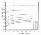
도 1은 OLED 효율, OLED 노화, 및 OLED 구동전류 밀도 간의 관계를 나타낸 그래프이다.
도 2는 본 발명의 실시에 사용될 수 있는 전계발광(EL) 디스플레이의 일실시예의 개략도이다.
도 3은 본 발명의 실시예에 사용될 수 있는 EL 서브픽셀 및 연결된 구성부품들의 일실시예의 개략도이다.
도 4a는 휘도 효율에 대한 OLED 이미터의 노화효과를 나타낸 도표이다.
도 4b는 이미터 전류에 대한 OLED 이미터 또는 드라이브 트랜지스터의 노화 효과를 나타낸 도표이다.
도 5는 본 발명의 방법의 일실시예의 블록도이다.
도 6은 OLED 효율과 OLED 전압의 변화 간에 관계를 나타낸 그래프이다.1 is a graph showing the relationship between OLED efficiency, OLED aging, and OLED drive current density.
2 is a schematic diagram of one embodiment of an electroluminescent (EL) display that may be used in the practice of the present invention.
3 is a schematic diagram of one embodiment of EL subpixels and connected components that can be used in the embodiment of the present invention.
4A is a chart showing the aging effect of OLED emitters on luminance efficiency.
4B is a plot showing the aging effect of an OLED emitter or drive transistor on emitter current.
5 is a block diagram of one embodiment of a method of the present invention.
6 is a graph showing the relationship between OLED efficiency and change in OLED voltage.
도 2를 참조하면, 본 발명의 실시예에 사용될 수 있는 전계발광(EL) 디스플레이의 일실시예의 개략도가 도시되어 있다. EL 디스플레이(10)는 행렬로 배열된 기설정된 개수의 EL 서브픽셀들(60)의 어레이를 구비한다. EL 디스플레이(10)는 복수의 행 셀렉트 라인(20)을 포함하고, EL 서브픽셀(60)의 각 행은 행 셀렉트 라인(20)을 갖는다. EL 디스플레이(10)는 복수의 리드아웃 라인(30)을 포함하고, EL 서브픽셀(60)의 각 열은 리드아웃 라인(30)을 갖는다. 각 리드아웃 라인(30)은 제 3 스위치(30)에 연결되어 있고, 상기 스위치는 캘리브레이션 공정 동안 리드아웃 라인(30)을 전류소스(160)에 연결시킨다. 도면을 명확히 하기 위해 미도시하였으나, 각 열의 EL 서브픽셀(60)은 또한 해당기술분야에 잘 알려진 데이터 라인을 갖는다. 복수의 리드아웃 라인(30)은 하나 이상의 멀티플렉서(40)에 연결되어 있고, 멀티플렉서는 명백한 바와 같이 EL 서브픽셀(60)로부터 신호의 병렬/순차적 리드아웃을 허용한다. 멀티플렉서(40)는 EL 디스플레이(10)와 동일한 구조의 일부가 될 수 있거나, EL 디스플레이(10)로부터 연결 또는 분리될 수 있는 별도의 구조가 될 수 있다. "행" 및 "열"은 패널의 임의의 특정 방향을 의미하지 않는 것에 유의하라.2, a schematic diagram of one embodiment of an electroluminescent (EL) display that can be used in an embodiment of the present invention is shown. The
도 3을 참조하면, 본 발명의 실시예에 사용될 수 있는 EL 서브픽셀의 일실시예의 개략도가 도시되어 있다. EL 서브픽셀(60)은 EL 이미터(50), 드라이브 트랜지스터(70), 커패시터(75), 리드아웃 트랜지스터(80), 및 셀렉트 트랜지스터(90)를 포함한다. 각각의 트랜지스터는 제 1 전극, 제 2 전극 및 게이트 전극을 갖는다. 제 1 전압소스(140)가 제 1 스위치(110)에 의해 드라이브 트랜지스터(70)의 제 1 전극에 선택적으로 연결되며, 제 1 스위치는 EL 디스플레이 기판 또는 별도의 구조물에 위치될 수 있다. 연결은 소자들이 직접 연결되거나 또 다른 구성요소, 예컨대, 스위치, 다이오드, 또는 또 다른 트랜지스터를 통해 전기연결되는 것을 의미한다. 드라이브 트랜지스터(70)의 제 2 전극은 EL 이미터(50)에 연결되고, 제 2 전압소스(150)는 제 2 스위치(120)에 의해 EL 이미터(50)에 선택적으로 연결될 수 있으며, 제 2 스위치는 EL 디스플레이 기판에서 떨어져 있을 수 있다. EL 이미터(50)가 또한 제 2 전압소스(150)에 직접 연결될 수 있다. 적어도 하나의 제 1 스위치와 제 2 스위치(120)가 EL 디스플레이용으로 제공된다. EL 디스플레이가 다수의 전력구동 픽셀 서브그루핑을 갖는다면 추가적인 제 1 및 제 2 스위치가 제공될 수 있다. 드라이브 트랜지스터(70)는 역바이어스로 동작함으로써 제 1 스위치(100)로서 사용될 수 있어, 실질적으로 어떠한 전류도 흐르지 않는다. 역바이어스로 트랜지스터를 동작하는 방법이 해당기술분야에 공지되어 있다. 통상적인 디스플레이 모드에서, 제 1 및 제 2 스위치는 닫히는 반면, (후술된) 다른 스위치들은 개방된다. 드라이브 트랜지스터(70)의 게이트 전극은 트랜지스터(90)를 선택하도록 연결되어 해당기술분야에 잘 알려진 바와 같이 트랜지스터(70)를 구동하도록 데이터 라인(35)으로부터 데이터를 선택적으로 제공한다. 복수의 행 셀렉트 라인(20) 각각은 EL 서브픽셀(60)의 해당하는 행에 있는 셀렉트 트랜지스터(90)의 게이트 전극에 연결되어 있다. 셀렉트 트랜지스터(90)의 게이트 전극은 리드아웃 트랜지스터(80)의 게이트 전극에 연결되어 있다.Referring to Fig. 3, a schematic diagram of one embodiment of an EL subpixel that can be used in the embodiment of the present invention is shown. The
리드아웃 트랜지스터(80)의 제 1 전극은 드라이브 트랜지스터(70)의 제 2 전극과 EL 이미터(50)에 연결되어 있다. 복수의 리드아웃 라인(30) 각각은 서브픽셀(60)의 해당 열에 있는 리드아웃 트랜지스터(80)의 제 2 전극에 연결되어 있다. 리드아웃 라인(30)은 제 3 스위치(130)에 연결되어 있다. 각각의 제 3 스위치(130)(S3)가 EL 서브픽셀(60)의 각 열에 제공된다. 제 3 스위치는 전류소스(160)가 리드아웃 트랜지스터(80)의 제 2 전극에 선택적으로 연결되게 한다. 제 3 스위치에 의해 연결될 때 전류소스(160)는 기설정된 일정한 전류가 EL 서브픽셀(60)로 흐르게 한다. 제 3 스위치(130)와 전류소스(160)는 EL 디스플레이 기판 상에 또는 기판에 떨어져 제공될 수 있다. 전류소스(160)는 고임피던스(Hi-Z) 모드로 설정함으로써 제 3 스위치(130)로서 사용될 수 있어 실질적으로 전혀 전류가 흐르지 않도록 한다. 전류소스를 고임피던스 모드로 설정하는 방법은 해당기술분야에 공지되어 있다.The first electrode of the
리드아웃 트랜지스터(180)의 제 2 전극도 또한 전압측정회로(170)에 연결되고, EL 서브픽셀(60)의 특징을 나타내는 신호를 제공하기 위해 전압을 측정한다. 전압측정회로(170)는 전압 측정을 디지털신호로 변환하는 아날로그-디지털 컨버터(185)와 프로세서(190)를 포함한다. 아날로그-디지털 변환기(185)로부터의 신호가 프로세서(190)로 보내진다. 전압측정회로(170)는 또한 전압측정을 저장하기 위한 메모리(195)와 저역통과필터(180)를 포함할 수 있다. 전압측정회로(170)는 멀티플렉서 출력라인(45)과 멀티플렉서(40)를 통해 EL 서브픽셀(60)의 기설정된 개수로부터 전압을 순차적으로 판독하기 위한 복수의 리드아웃 라인(30)과 리드아웃 트랜지스터(80)에 연결될 수 있다. 복수의 멀티플렉서(40)가 있다면, 각각은 자신의 멀티플렉서 출력라인(45)을 가질 수 있다. 따라서, 기설정된 개수의 EL 서브픽셀(60)이 동시에 구동될 수 있다. 복수의 멀티플렉서(40)는 다양한 멀티플렉서(40)로부터 전압의 병렬식 리드아웃을 허용하는 반면, 각 멀티플렉서(40)는 부착된 리드아웃 라인(30)의 순차적 리드아웃을 허용한다. 이를 본 명세서에서 병렬/순차 프로세스라 한다.The second electrode of the
프로세서(190)는 또한 컨트롤 라인(95)과 소스 드라이버(155)에 의해 데이터 라인(35)에 연결될 수 있다. 따라서, 프로세서(190)는 본 명세서에 기술된 측정 프로세스 동안 데이터 라인(35)에 기설정된 데이터 값을 제공할 수 있다. 프로세서(190)는 또한 입력신호(85)를 통해 디스플레이 데이터를 수용할 수 있고 본 명세서에 상술한 바와 같이 변화에 대한 보상을 제공할 수 있어, 디스플레이 프로세스 동안 데이터 라인(35)에 보상된 데이터를 제공할 수 있다. 소스 드라이버(155)는 디지털-아날로그 컨버터 또는 프로그램가능한 전압소스, 프로그래가능한 전류소스, 또는 펄스폭변조전압("디지털 드라이드") 또는 전류 드라이버 또는 해당기술분야에 공지된 또 다른 타입의 소스 드라이버를 구비할 수 있다.
도 3에 도시된 실시예는 비역전 NMOS 서브픽셀이다. 해당기술분야에 공지된 다른 형태가 본 발명에 이용될 수 있다. EL 이미터(50)는 해당기술분야에 공지된 OLED 이미터 또는 다른 이미터 타입일 수 있다. EL 이미터(50)가 OLED 이미터이면, EL 서브픽셀(60)은 OLED 서브픽셀이다. 드라이브 트랜지스터(70) 및 다른 트랜지스터(80,90)는 저온 폴리실리콘(LPTS), 아연산화물(ZnO), 또는 비정질 실리콘(a-Si) 트랜지스터일 수 있거나 해당기술분야에 공지된 또 다른 타입의 트랜지스터이다.The embodiment shown in FIG. 3 is a non-inverting NMOS subpixel. Other forms known in the art can be used in the present invention.
각 트랜지스터(70,80,90)는 N채널 또는 P채널일 수 있고, EL 이미터(50)는 역전 또는 비역전 배열로 드라이브 트랜지스터(70)에 연결될 수 있다. 해당기술분야에 공지된 역전 형태로, 제 1 및 제 2 전원의 극성이 바뀌고, EL 이미터(50)는 드라이버 트랜지스터로부터 멀어지기보다 드라이버 트랜지스터를 향해 전류를 전도시킨다. 따라서, 본 발명의 전류소스(160)는 음의 전류로서 나와야 한다. 즉, 전류싱크로서 행동해 EL 이미터(50)를 통해 전류를 인출한다.Each
EL 이미터(50), 예컨대, OLED 이미터가 사용되면, 종종 cd/A라고 하는 발광 효율이 줄어들 수 있고 저항이 증가할 수 있다. 이들 효과 모두는 EL 이미터에 의해 방출된 광량이 시간에 걸쳐 줄어들게 할 수 있다. 이런 감소량은 EL 이미터의 사용에 따른다. 따라서, 감소는 디스플레이내 다른 EL 이미터에 대해 다를 수 있고, 그 효과는 본 명세서에서 EL 이미터(50)의 특징에서 공간적 변화라 한다. 이런 공간적 변화는 디스플레이의 다른 부분에서 밝기 및 컬러 밸런스에서 차이를 포함하고, 자주 디스플레이되는 이미지(예컨대, 네트워크 로고)로서 자체의 고스트가 능동 디스플레이상에 항상 보이도록 "번-인(burn-in)을 영상화할 수 있다. 이런 문제를 방지하기 위해 임계전압의 이런 변화를 보상하는 것이 바람직하다.When an
도 4a를 참조하면, 전류가 OLED 이미터를 지날 때 휘도 효율에서 OLED 이미터의 노화 효과를 나타낸 도표가 도시되어 있다. 3개 곡선은 시간 또는 누적전류에 걸쳐 출력된 광으로 표현되는 다른 컬러의 광(예컨대, 적색광, 녹색광, 및 청색광 이미터를 각각 나타내는 R,G,B)을 방출하는 다른 광 이미터의 대표적인 성능을 나타낸다. 다른 컬러의 광 이미터들 간에 휘도의 감소가 다를 수 있다. 차이는 다른 컬러의 광 이미터에 사용된 재료의 다른 노화특징 또는 다른 컬러의 광 이미터의 다른 용도로 인한 것일 수 있다. 따라서, 노화 보정이 없는 종래의 사용시, 디스플레이는 밝기가 덜해질 수 있고 디스플레이의 컬러, 특히 백색점이 이동될 수 있다.Referring to FIG. 4A, a diagram showing the aging effect of an OLED emitter in luminance efficiency as current passes through the OLED emitter. Three curves represent representative performance of different light emitters emitting different color light (e.g., R, G, B representing red light, green light, and blue light emitter, respectively) represented as light output over time or cumulative current. Indicates. The reduction in luminance may differ between light emitters of different colors. The difference may be due to different aging characteristics of the materials used for the light emitters of different colors or other uses of the light emitters of different colors. Thus, in conventional use without aging correction, the display may be less bright and the color of the display, in particular the white point, may be shifted.
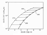
도 4b를 참조하면, 이미터 전류에 대한 OLED 이미터 또는 드라이브 트랜지스터 또는 둘 다의 노화효과를 나타내는 도면이 도시되어 있다. 도 4b의 가로좌표는 드라이브 트랜지스터(70)에서 게이트 전압을 나타내고, 세로좌표는 게이트 전압에서 드라이브 트랜지스터를 통한 전류의 밑을 10으로 한 로그를 나타낸다. 초기 곡선(230)은 노화 전의 서브픽셀을 나타낸다. 서브픽셀이 노화됨에 따라, 더 큰 전압이 소정의 전류를 얻는데 필요하다; 즉, 상기 곡선은 양 ΔV만큼 노화곡선(240)으로 이동된다. ΔV는 도시된 바와 같이 임계전압의 변화(ΔVth, 210)와 OLED 이미터 저항에서 변화로 인해 발생한 OLED 전압의 변화(ΔVOLED, 220)의 합이다. 이 변화로 인해 성능이 저하된다. 더 큰 게이트 전압이 소정의 전류를 얻는데 요구된다. 드라이브 트랜지스터를 지나는 드레인-소스 전류인 OLED 전류, OLED 전압 및 포화시 임계전압 간의 관계는 다음과 같다:Referring to FIG. 4B, a diagram illustrating the aging effect of an OLED emitter or drive transistor or both on emitter current is shown. The abscissa of FIG. 4b represents the gate voltage in the

여기서, W는 TFT 채널폭이고, L은 TFT 채널길이이며, μ는 TFT 이동도이고, C0는 단위면적당 산화물 커패시턴스이며, Vg는 게이트 전압이고, Vgs는 드라이브 트랜지스터의 게이트와 소스 간의 전압차이다. 간략히 하기 위해, Vgs에 대한 μ의 의존성을 무시한다. 따라서, 전류를 일정하게 유지하기 위해, Vth 및 VOLED의 변화를 보상해야 한다. Where W is the TFT channel width, L is the TFT channel length, μ is the TFT mobility, C 0 is the oxide capacitance per unit area, V g is the gate voltage, and V gs is the voltage between the gate and source of the drive transistor. It's a car. For simplicity, ignore the dependence of μ on V gs . Therefore, in order to keep the current constant, changes in V th and V OLED must be compensated for.
도 5와 또한 도 3을 참조하면, 본 발명의 방법의 일실시예의 블록도가 도시되어 있다. 5 and 3, there is shown a block diagram of one embodiment of the method of the present invention.
EL 이미터(50)의 특징을 측정하기 위해, 제 1 스위치(110)가 열리고, 제 2 스위치(120) 및 제 3 스위치(130)가 닫힌다(단계 340). 셀렉트 라인(20)은 선택된 행에 대해 활성화되어 리드아웃 트랜지스터(80)를 온시킨다(단계 345). 따라서, 전류 Itestsu가 전류소스(60)로부터 EL 이미터(50)를 통해 제 2 전압소스(150)로 흐른다. 전류소스(160)를 통한 전류값은 EL 이미터(50)를 지나는 가능한 최대 전류보다 적게 선택된다; 일반적인 값은 1 내지 5 마이크로암페어 범위에 있고 EL 서브픽셀의 수명 동안 모든 측정들에 대해 일정해 진다. 하나 이상의 특정값이 이 과정에서 사용될 수 있다. 예컨대, 1, 2, 및 3 마이크로암페어에서 측정이 수행될 수 있다. 하나 이상의 측정값에서 측정을 함으로써 EL 서브픽셀(60)의 완전한 I-V 곡선이 형성된다. 전압측정회로(170)는 리드아웃 라인(30)상에 전압을 측정하는데 사용될 수 있다(단계 350). 이 전압은 리드아웃 트랜지스터(80)의 제 2 전극에서 전압(Vout)이고, 저항과 이에 따른 EL 이미터(0)의 효율을 포함한 EL 이미터(50)의 특징을 나타내는 제 1 이미터 전압신호(V2)를 제공하는데 사용될 수 있다.In order to measure the characteristics of the
서브픽셀에서 구성부품들의 전압은 다음과 관계 있다:The voltages of the components in the subpixels are related to:
![]()
![]()
이들 전압값으로 리드아웃 트랜지스터(80)(Vout)의 제 2 전극에서의 전압이 수학식 2를 수행하도록 조절게 한다. 상술한 조건 하에서, CV는 세트값이고 Vread는 리드아웃 트랜지스터를 지나는 전류가 낮고 시간에 걸쳐 크게 변하지 않는 상수인 것으로 가정할 수 있다. VOLED는 전류소스(160)에 의해 설정된 전류값과 전류-전압특성에 의해 제어된다.These voltage values allow the voltage at the second electrode of the readout transistor 80 (V out ) to be adjusted to perform equation (2). Under the conditions described above, it can be assumed that CV is a set value and V read is a constant with a low current through the readout transistor and does not change significantly over time. V OLED is controlled by the current value and current-voltage characteristic set by the
VOLED는 EL 이미터(50)에서 노화관련 변화에 따라 변할 수 있다. VOLED의 변화를 판단하기 위해, 시간을 달리해 2개의 별도의 테스트 측정을 수행한다. 제 1 측정은 제 1 시간, 예컨대, EL 이미터(50)가 노화에 의해 열화되지 않을 때에 수행된다. 이는 EL 서브픽셀(60)이 디스플레이 용으로 사용되기 전의 임의의 시간일 수 있다. 제 1 측정에 대한 전압값(V2)은 제 1 이미터-전압 신호(이하 V2a)이고, 측정 및 저장된다. 제 1 시간과는 다른 제 2 시간에, 예컨대, EL 이미터(50)가 기설정된 시간에 대한 이미지를 디스플레이함으로써 노화된 후에, 측정이 반복되고 제 2 이미터-전압 신호(이하 V2b)가 저장된다.The V OLED may change with age related changes in the
피측정 행에 추가 EL 서브픽셀이 있는 경우, 복수의 리드아웃 라인(30)에 연결된 멀티플렉서(40)는 전압측정회로(170)가 연이어 기설정된 개수의 EL 서브픽셀들, 예컨대, 행에서 모든 서브픽셀들 각각을 측정하도록 사용되고(판단단계 355), 각 서브픽셀에 대해 해당하는 제 1 및 제 2 이미터-전압 신호를 제공한다. 디스플레이가 충분히 크면, 제 1 및 제 2 이미터-전압 신호가 병렬/순차 프로세스에 제공되는 복수의 멀티플렉서를 필요로 할 수 있다. EL 디스플레이(10)에서 피측정 서브픽셀의 추가 행들이 있다면, 단계 345 내지 355가 각 행에 대해 반복된다(판단단계 360). 측정 프로세스를 가속화하기 위해, 기설정된 개수의 EL 서브픽셀들 각각은 측정을 취할 때 임의의 정한 시간을 경과하도록 동시에 구동될 수 있다.When there are additional EL subpixels in a row under test, the
EL 이미터(50)에서 변화로 인해 VOLED의 변화가 테스트 전류 Itestsu를 유지하게 할 수 있다. 이들 VOLED 변화는 V2에 대한 변화에 반영된다. 따라서, 각 EL 서브픽셀(60)에 대한 2개의 저장된 이미터-전압 신호(V2) 측정은 EL 이미터(50)의 효율을 나타내는 노화신호(ΔV2)를 계산하기 위해 다음과 같이 비교될 수 있다:The change in the
![]()
![]()
상기 방법은 추후 비교를 위해 각 서브픽셀에 대한 해당하는 제 1 이미터-전압 신호가 메모리에 저장되는 것을 필요로 한다. 초기 측정을 필요로 하지 않고 VOLED에서 공간 변화를 보상할 수 있는 덜 메모리 집약적인 방법이 사용될 수 있다. 노화 후, 제 2 이미터-전압 신호(V2b)가 상술한 바와 같이 전류소스(60)에 대해 선택된 값들에 따라 각 서브픽셀에 대해 기록될 수 있다. 그런 후, 최소 VOLED 변위(즉, 측정된 최소 V2b)를 갖는 서브픽셀이 타겟 신호가 되도록 측정된 서브픽셀의 모집단으로부터 선택된다. 이 타겟신호는 모든 서브픽셀들에 대해 제 1 이미터-전압 신호(V2a , tgt)로서 사용된다. 각각의 복수의 서브 픽셀들에 대한 노화신호(ΔV2)는 다음과 같이 표현될 수 있다:The method requires that the corresponding first emitter-voltage signal for each subpixel is stored in memory for later comparison. Less memory-intensive methods can be used that can compensate for spatial variations in V OLEDs without requiring an initial measurement. After aging, a second emitter-voltage signal V 2b may be recorded for each subpixel according to the values selected for
![]()
![]()
그런 후, EL 서브픽셀(60)에 대한 노화신호는 EL 서브픽셀의 특징에 있어 변화를 보상하는데 사용될 수 있다. Then, the aging signal for the
EL 노화를 보상하기 위해, (ΔV2에 대한)ΔVOLED에 대해 상술한 바와 같이 보정하는 것이 필요하다. 그러나, 제 2 인자는 또한 EL 이미터의 휘도와 노화 또는 사용에 따른 변화에 영향을 준다: EL 이미터의 효율은 사용에 따라 감소되고, 이는 (도 4a에 도시된 바와 같이)소정의 전류에서 광 방출을 저하시킨다. 상기 관계 이외에, EL 이미터의 휘도효율의 감소와 ΔVOLED 간에 관계, 즉, 소정 전류에 대한 EL 휘도가 ΔVOLE 에서 변화 함수인 관계가 다음과 같이 밝혀졌다:To compensate for EL aging, it is necessary to calibrate as described above for ΔV OLEDs (for ΔV 2 ). However, the second factor also affects the brightness and aging of the EL emitter and changes with use: the efficiency of the EL emitter decreases with use, which is at a given current (as shown in FIG. 4A). Reduces light emission. In addition to the above relationship, the relationship between the decrease in the luminance efficiency of the EL emitter and the ΔV OLED , that is, the relationship that the EL brightness for a predetermined current is a change function in the ΔV OLE , is found as follows:

휘도효율과 테스트 OLED 이미터에 대한 ΔVOLED 간의 관계의 예가 도 6에 그래프로 도시되어 있다. 도 6은 부호의 설명에 나열된 다양한 페이드 전류밀도(fade current density)로 이 관계를 나타내고 있다. 도시된 바와 같이, 상기 관계는 페이드 전류밀도에 대략 무관한 것으로 실험적으로 판단되었다. 휘도감소와 소정의 전류에 따른 ΔVOLED 간의 관계를 측정함으로써, EL 이미터(50)가 공칭 휘도를 출력하도록 하는데 필요한 보정된 신호의 변화가 결정될 수 있다. 이 측정은 모델 시스템상에 행해질 수 있고 그런 후 참조표에 저장되거나 알고리즘으로서 사용될 수 있다. 이 모델링은 더 정확한 결과를 위해 다양한 페이드 전류밀도로 또는 비용을 줄이고 OLED 전압 상승과 OLED 효율 손실 간의 관계가 대략 페이드 전류밀도에 무관하다는 도 6에 도시된 판단을 이용해 하나의 페이드 전류밀도로 수행될 수 있다. An example of the relationship between the luminance efficiency and the ΔV OLED for the test OLED emitter is shown graphically in FIG. 6. Figure 6 illustrates this relationship with the various fade current densities listed in the description of the sign. As shown, the relationship was experimentally determined to be approximately independent of the fade current density. By measuring the relationship between the luminance reduction and the ΔV OLED according to a predetermined current, the change in the corrected signal necessary for causing the
EL 서브픽셀(60)의 특징에서 상기 변화를 보상하기 위해, 입력신호(Vdata)가 수신된다(단계 375). 그런 후, 노화신호 및 입력신호가 보상 구동신호를 생성하기 위해 사용될 수 있다(단계 380). 하기의 형태의 방정식이 사용될 수 있다:To compensate for this change in the characteristics of the
![]()
![]()
여기서, ΔVdata는 소정의 휘도를 유지하는데 필요한 드라이브 트랜지스터(70)의 게이트 전극에 대한 오프세트 전압이고, f2(ΔV2)는 EL 저항의 차에 대한 보상이고, f3(ΔV2)는 EL 효율의 변화에 대한 보상이다. 이 경우, 보상 구동신호(Vcomp)는 다음과 같다:Here, ΔV data is an offset voltage for the gate electrode of the
![]()
![]()
보상 구동신호(Vcomp)는 드라이버 트랜지스터의 게이트 전극에 제공되어 소스 드라이버(155)를 이용해 EL 이미터의 효율과 전압 변화를 보상한다(단계 385).The compensation driving signal V comp is provided to the gate electrode of the driver transistor to compensate for the efficiency and voltage change of the EL emitter using the source driver 155 (step 385).
복수의 EL 서브픽셀을 갖는 EL 디스플레이를 보상할 때, 각 서브픽셀은 복수의 해당하는 제 1 및 제 2 이미터 전압신호를 제공하도록 측정되고, 상술한 바와 같이 복수의 해당하는 노화신호가 제공된다. 각 서브픽셀에 대한 해당하는 입력신호가 수신되고 해당하는 보상 구동신호가 해당하는 노화신호를 이용해 상기와 같이 계산된다. 복수의 서브픽셀에서 각 서브픽셀에 해당하는 보상 구동신호가 해당기술분야에 공지된 바와 같이 소스 드라이버(155)를 이용해 상기 서브픽셀의 게이트 전극에 제공된다. 이는 복수의 EL 서브픽셀에서 각 EL 서브픽셀의 효율에서의 변화를 보상하게 한다.When compensating an EL display having a plurality of EL subpixels, each subpixel is measured to provide a plurality of corresponding first and second emitter voltage signals, and a plurality of corresponding aging signals are provided as described above. . The corresponding input signal for each subpixel is received and the corresponding compensation drive signal is calculated as above using the corresponding aging signal. A compensation driving signal corresponding to each subpixel in the plurality of subpixels is provided to the gate electrode of the subpixel using the
EL 디스플레이는 컨트롤러를 포함할 수 있고, 컨트롤러는 각 EL 이미터에 대한 오프세트 전압을 계산하기 위해 참조표 또는 알고리즘을 포함할 수 있다. 오프세트 전압이 계산되어 구동 트랜지스터(70)의 임계전압에서의 변화로 인한 전류의 변화와 EL 이미터(50)의 노화에 대한 보정을 제공할 뿐만 아니라 EL 이미터(50)의 노화로 인한 효율손실을 보상하기 위해 전류 증가를 제공하며, 따라서 완전한 EL 노화 보상방안을 제공한다. 이들 변화는 소정의 공칭 휘도값으로 광출력을 보정하도록 컨트롤러에 의해 적용된다. EL 이미터에 적용된 신호를 제어함으로써, 휘도출력이 일정하고 수명이 증가된 EL 이미터가 달성된다. 이 방법은 디스플레이에서 각 EL 이미터에 대한 보정을 제공하기 때문에, 복수의 EL 서브픽셀 특징에서 공간 변화 및 특히 각 EL 이미터의 효율에서 변화를 보상한다.The EL display may include a controller, which may include a look-up table or algorithm to calculate the offset voltage for each EL emitter. The offset voltage is calculated to provide correction for changes in current due to changes in the threshold voltage of the
도 1을 참조하면, OLED 이미터의 휘도효율과 이미터가 구동되는 전류밀도 간에 추가 관계가 발견된다. 일반적으로, OLED 이미터는 전류, 전류밀도, 또는 주어진 OLED 이미터에 대한 전류밀도의 바이젝티브리 지도로 나타내는 나타내는 임의의 다른 값으로 표현되는 구동레벨로 인해 OLED 효율에서 변화를 나타낼 수 있다. 이 관계는 더 정확한 모델을 위해 상기 수학식 5로 표현된 관계와 조합될 수 있어 주어진 전류에 대한 OLED 휘도가 다음과 같이 주어진다:Referring to FIG. 1, a further relationship is found between the luminance efficiency of OLED emitters and the current density at which the emitters are driven. In general, an OLED emitter may exhibit a change in OLED efficiency due to the drive level represented by current, current density, or any other value represented by a objective map of the current density for a given OLED emitter. This relationship can be combined with the relationship represented by Equation 5 above for a more accurate model so that the OLED brightness for a given current is given by:

여기서, ΔVOLED는 상술한 바와 같이 다시 측정된 전류 Itestsu로 인한 OLED 전압에 대한 변화이고, Ids는 구동 입력신호(85)로부터 이상적으로 발생한 OLED를 지나는 전류이다(도 3). 입력신호(85)의 값 또는 다른 구동레벨 값들이 이 수학식에서 Ids로 대체될 수 있다. 도 1에서 각 곡선은 Ids를 이미터 면적으로 나눈 전류밀도와 특정지점에 대해 노화된 OLED에 대한 효율(LOLED/IOLED) 간에 관계를 도시한 것이다. 노화는 해당기술분야에 공지된 T 표시를 이용해 부호의 설명에 나타나 있다: 예컨대, T86은 이 경우 20mA/㎠의 테스트 전류밀도에서 86%의 효율을 의미한다.Here, ΔV OLED is the change in OLED voltage due to the current I testsu measured again as described above, and Ids is the current through the OLED ideally generated from the drive input signal 85 (FIG. 3). The value of the
EL 서브픽셀(60), 예컨대, OLED 서브픽셀의 특징에서 상기 변화를 보상하기 위해, 하기의 방정식 형태의 입력신호를 수반한 수학식 8을 포함한 상술한 모델에 따라 노화신호(ΔV2)를 사용할 수 있다:In order to compensate for this change in the characteristics of an
![]()
![]()
여기서, ΔVdata는 소정의 휘도를 유지하는데 필요한 드라이브 트랜지스터(70)의 게이트 전극에 대한 오프세트 전압이고, f2(ΔV2)는 EL 저항의 변화에 대한 보상이며, f3(ΔV2,Ids)는 명령된 전류 Ids에서 EL 효율의 변화에 대한 보상이다. 함수 f3는 도 1에 도시된 곡선과 같은 곡선의 피트(fit)일 수 있다. 상기와 같이, 임의의 구동 레벨값이 수학식 9의 두번째 항에 사용될 수 있다. 그런 후, 수학식 9로부터 ΔVdata 값은 보상 구동신호를 제공하기 위해 수학식 7에 사용될 수 있다. 이는 더 정확한 보상방안을 제공할 수 있다.Here, ΔV data is an offset voltage with respect to the gate electrode of the
바람직한 실시예에서, 본 발명은 탕 등(Tang et al.)의 미국특허 No. 4,769,292 및 반슬리케 등(VanSlyke et al.)의 미국특허 No. 5,061,569에 개시되어 있으나 이에 국한되지 않는 작은 분자 또는 폴리머 OLED로 구성된 유기발광 다이오드(OLEDs)를 포함하는 디스플레이에 사용된다. 이런 디스플레이를 제조하는데 유기발광 디스플레이의 많은 조합과 변화들이 사용될 수 있다. In a preferred embodiment, the present invention is described in US Pat. 4,769,292 and Van Slyke et al., US Pat. Used in displays comprising organic light emitting diodes (OLEDs) comprised of small molecule or polymer OLEDs as disclosed in, but not limited to, 5,061,569. Many combinations and variations of organic light emitting displays can be used to make such displays.
10 EL 디스플레이
20 셀렉트 라인
30 리드아웃 라인
35 데이터 라인
40 멀티플렉서
45 멀티플렉서 출력라인
50 EL 이미터
60 EL 서브픽셀
70 드라이브 트랜지스터
75 커패시터
80 리드아웃 트랜지스터
85 입력신호
90 셀렉트 트랜지스터
95 컨트롤 라인
110 제 1 스위치
120 제 2 스위치
130 스위치 블록
140 제 1 전압소스
150 제 2 전압소스
155 소스 드라이버
160 전류소스
165 전류싱크
170 전압측정회로
180 저역통과필터
185 아날로그-디지털 컨버터
190 프로세서
195 메모리
210 ΔVth
220 ΔVOLED
230 초기 곡선
240 노화 곡선
340 단계
345 단계
350 단계
355 판단단계
360 판단단계
370 단계
375 단계
380 단계
385 단계10 EL display
20 select lines
30 lead-out lines
35 data lines
40 multiplexer
45 Multiplexer Output Lines
50 EL emitter
60 EL subpixels
70 drive transistor
75 capacitor
80 lead-out transistors
85 Input Signal
90 select transistor
95 control lines
110 first switch
120 second switch
130 switch blocks
140 first voltage source
150 second voltage source
155 source driver
160 current source
165 Current Sink
170 voltage measuring circuit
180 Low Pass Filter
185 analog-to-digital converters
190 processor
195 memory
210 ΔV th
220 ΔV OLED
230 initial curve
240 Aging Curve
340 steps
345 steps
350 steps
355 Decision Stage
360 judgment steps
370 steps
375 steps
380 steps
385 steps
Claims (14)
b) 제 1 전압소스를 드라이브 트랜지스터의 제 1 전극에 선택적으로 연결하기 위해 제 1 전압소스와 제 1 스위치를 제공하는 단계와,
c) EL 이미터를 드라이브 트랜지스터의 제 2 전극에 연결하는 단계와,
d) EL 이미터에 연결된 제 2 전압소스를 제공하는 단계와,
e) 리드아웃 트랜지스터의 제 1 전극을 드라이브 트랜지스터의 제 2 전극에 연결하는 단계와,
f) 전류소스를 리드아웃 트랜지스터의 제 2 전극에 선택적으로 연결하기 위해 전류소스와 제 3 스위치를 제공하는 단계와,
g) 리드아웃 트랜지스터의 제 2 전극에 연결된 전압측정회로를 제공하는 단계와,
h) 제 1 스위치를 열고 제 3 스위치를 닫으며, 전압측정회로를 이용해 리드아웃 트랜지스터의 제 2 전극에서의 전압을 측정하여 제 1 이미터 전압신호를 제공하는 단계와,
i) 제 1 이미터 전압신호를 이용해 EL 이미터의 효율을 나타내는 노화신호를 제공하는 단계와,
j) 입력신호를 수신하는 단계와,
k) 노화신호와 입력신호를 이용해 보상 구동신호를 생성하는 단계와,
l) EL 이미터의 효율에서의 변화를 보상하기 위해 드라이브 트랜지스터의 게이트 전극에 보상 구동신호를 제공하는 단계를 포함하는 전계발광(EL) 서브픽셀내 드라이브 트랜지스터의 게이트 전극에 구동신호를 제공하는 방법.a) providing a drive transistor having a first electrode, a second electrode, and a gate electrode, an EL subpixel having an EL emitter, and a readout transistor;
b) providing a first voltage source and a first switch for selectively connecting the first voltage source to the first electrode of the drive transistor;
c) connecting the EL emitter to the second electrode of the drive transistor,
d) providing a second voltage source connected to the EL emitter;
e) connecting the first electrode of the readout transistor to the second electrode of the drive transistor;
f) providing a current source and a third switch to selectively connect the current source to the second electrode of the readout transistor;
g) providing a voltage measurement circuit connected to a second electrode of the readout transistor;
h) opening the first switch and closing the third switch, measuring a voltage at the second electrode of the readout transistor using a voltage measurement circuit to provide a first emitter voltage signal;
i) providing an aging signal indicative of the efficiency of the EL emitter using the first emitter voltage signal;
j) receiving an input signal;
k) generating a compensation driving signal using the aging signal and the input signal;
l) providing a drive signal to the gate electrode of the drive transistor in an electroluminescent (EL) subpixel, comprising providing a compensation drive signal to the gate electrode of the drive transistor to compensate for variations in the efficiency of the EL emitter. .
EL 이미터를 제 2 전압소스에 선택적으로 연결하기 위해 제 2 스위치를 제공하는 단계를 더 포함하고, 단계 h)는 제 2 스위치를 닫는 단계를 포함하는 전계발광(EL) 서브픽셀내 드라이브 트랜지스터의 게이트 전극에 구동신호를 제공하는 방법.The method of claim 1,
Providing a second switch to selectively connect the EL emitter to the second voltage source, wherein step h) comprises closing the second switch. A method of providing a drive signal to a gate electrode.
단계 h)는
i) 제 1 이미터 전압신호를 제공하기 위해 제 1 시간에 리드아웃 트랜지스터의 제 2 전극에서 전압을 측정하는 단계와,
ⅱ) 제 1 이미터-전압 신호를 저장하는 단계와,
ⅲ) 제 1 시간과는 다른 제 2 시간에 제 2 이미터 전압신호를 측정하는 단계와,
ⅳ) 제 2 이미터 전압신호를 저장하는 단계를 더 포함하는 전계발광(EL) 서브픽셀내 드라이브 트랜지스터의 게이트 전극에 구동신호를 제공하는 방법.The method of claim 1,
Step h)
i) measuring a voltage at a second electrode of the readout transistor at a first time to provide a first emitter voltage signal;
Ii) storing the first emitter-voltage signal;
Iii) measuring the second emitter voltage signal at a second time different than the first time;
Iii) storing a second emitter voltage signal; providing a drive signal to a gate electrode of a drive transistor in an electroluminescent (EL) subpixel.
단계 i)는 노화신호를 제공하기 위해 저장된 제 1 및 제 2 이미터-전압 신호를 비교하는 단계를 더 포함하는 전계발광(EL) 서브픽셀내 드라이브 트랜지스터의 게이트 전극에 구동신호를 제공하는 방법.The method of claim 3, wherein
Step i) further comprises comparing the stored first and second emitter-voltage signals to provide an aging signal to provide a drive signal to the gate electrode of the drive transistor in the electroluminescent (EL) subpixel.
전압측정회로는 아날로그-디지털 컨버터를 포함하는 전계발광(EL) 서브픽셀내 드라이브 트랜지스터의 게이트 전극에 구동신호를 제공하는 방법.The method of claim 1,
The voltage measuring circuit provides a drive signal to a gate electrode of a drive transistor in an electroluminescent (EL) subpixel comprising an analog-to-digital converter.
전압측정회로는 저역통과필터를 더 포함하는 전계발광(EL) 서브픽셀내 드라이브 트랜지스터의 게이트 전극에 구동신호를 제공하는 방법.The method of claim 5, wherein
The voltage measuring circuit provides a drive signal to a gate electrode of a drive transistor in an electroluminescent (EL) subpixel further comprising a low pass filter.
복수의 EL 서브픽셀을 제공하는 단계를 더 포함하고, 복수의 해당하는 노화신호를 생성하기 위해 각 EL 서브픽셀에 대해 단계 h) 및 i)가 수행되며, 해당하는 노화신호를 이용해 복수의 서브픽셀 각각에 대해 단계 j) 및 l)이 수행되는 전계발광(EL) 서브픽셀내 드라이브 트랜지스터의 게이트 전극에 구동신호를 제공하는 방법.The method of claim 1,
Providing a plurality of EL subpixels, wherein steps h) and i) are performed for each EL subpixel to generate a plurality of corresponding aging signals, and using the corresponding aging signals; Providing a drive signal to the gate electrode of the drive transistor in the electroluminescent (EL) subpixel where steps j) and l) are performed for each.
기설정된 개수의 서브픽셀들이 동시에 구동되는 동안 기설정된 개수의 이런 EL 서브픽셀에 대해 단계 h)가 수행되는 전계발광(EL) 서브픽셀내 드라이브 트랜지스터의 게이트 전극에 구동신호를 제공하는 방법.The method of claim 7, wherein
A method for providing a drive signal to a gate electrode of a drive transistor in an electroluminescent (EL) subpixel in which step h) is performed on a predetermined number of such EL subpixels while a predetermined number of subpixels are simultaneously driven.
EL 서브픽셀은 행렬로 배열되고, 해당하는 셀렉트 트랜지스터의 게이트 전극에 연결된 복수의 행 셀렉트 라인들과 해당하는 리드아웃 트랜지스터의 제 2 전극에 연결된 복수의 리드아웃 라인들을 제공하는 단계를 더 포함하는 전계발광(EL) 서브픽셀내 드라이브 트랜지스터의 게이트 전극에 구동신호를 제공하는 방법.The method of claim 7, wherein
The EL subpixels are arranged in a matrix and further comprising providing a plurality of row select lines connected to the gate electrodes of the corresponding select transistors and a plurality of lead out lines connected to the second electrodes of the corresponding readout transistors. A method of providing a drive signal to a gate electrode of a drive transistor in a light emitting (EL) subpixel.
기설정된 개수의 EL 서브픽셀 각각을 순차적으로 측정하기 위해 복수의 리드아웃 라인들에 연결된 멀티플렉서를 이용해 해당하는 제 1 이미터-전압 신호를 제공하는 단계를 더 포함하는 전계발광(EL) 서브픽셀내 드라이브 트랜지스터의 게이트 전극에 구동신호를 제공하는 방법.The method of claim 9,
Providing a corresponding first emitter-voltage signal using a multiplexer connected to a plurality of leadout lines to sequentially measure each predetermined number of EL subpixels in the electroluminescent (EL) subpixel. A method of providing a drive signal to a gate electrode of a drive transistor.
드라이브 트랜지스터의 게이트 전극에 연결된 셀렉트 트랜지스터를 더 제공하는 단계를 포함하고, 셀렉트 트랜지스터의 게이트 전극은 리드아웃 트랜지스터의 게이트 전극에 연결되는 전계발광(EL) 서브픽셀내 드라이브 트랜지스터의 게이트 전극에 구동신호를 제공하는 방법.The method of claim 1,
And providing a select transistor coupled to the gate electrode of the drive transistor, wherein the gate electrode of the select transistor provides a drive signal to the gate electrode of the drive transistor in an electroluminescent (EL) subpixel connected to the gate electrode of the readout transistor. How to give.
각각의 EL 이미터는 OLED 이미터이며, 각 EL 서브픽셀은 OLED 서브픽셀인 전계발광(EL) 서브픽셀내 드라이브 트랜지스터의 게이트 전극에 구동신호를 제공하는 방법.The method of claim 1,
Wherein each EL emitter is an OLED emitter, and each EL subpixel is an OLED subpixel, providing a drive signal to a gate electrode of a drive transistor in an electroluminescent (EL) subpixel.
단계 l)은 소스 드라이버를 제공하는 단계와, 상기 소스 드라이버를 이용해 보상 구동신호를 드라이브 트랜지스터의 게이트 전극에 제공하는 단계를 더 포함하는 전계발광(EL) 서브픽셀내 드라이브 트랜지스터의 게이트 전극에 구동신호를 제공하는 방법.The method of claim 1,
Step l) further includes providing a source driver and providing a compensation drive signal to the gate electrode of the drive transistor using the source driver. The drive signal is applied to the gate electrode of the drive transistor in the EL subpixel. How to give it.
소스 드라이버는 디지털-아날로그 컨버터를 구비하는 전계발광(EL) 서브픽셀내 드라이브 트랜지스터의 게이트 전극에 구동신호를 제공하는 방법.The method of claim 13,
A source driver provides a drive signal to a gate electrode of a drive transistor in an electroluminescent (EL) subpixel having a digital-to-analog converter.
Applications Claiming Priority (2)
| Application Number | Priority Date | Filing Date | Title |
|---|---|---|---|
| US12/260,103 US8228267B2 (en) | 2008-10-29 | 2008-10-29 | Electroluminescent display with efficiency compensation |
| US12/260,103 | 2008-10-29 |
Related Child Applications (1)
| Application Number | Title | Priority Date | Filing Date |
|---|---|---|---|
| KR1020137015254A Division KR101419450B1 (en) | 2008-10-29 | 2009-10-27 | Electroluminescent Display with Compensation of Efficiency Variations |
Publications (1)
| Publication Number | Publication Date |
|---|---|
| KR20110074999A true KR20110074999A (en) | 2011-07-05 |
Family
ID=41361268
Family Applications (2)
| Application Number | Title | Priority Date | Filing Date |
|---|---|---|---|
| KR1020117009592A KR20110074999A (en) | 2008-10-29 | 2009-10-27 | Electroluminescent display with compensation of efficiency variations |
| KR1020137015254A KR101419450B1 (en) | 2008-10-29 | 2009-10-27 | Electroluminescent Display with Compensation of Efficiency Variations |
Family Applications After (1)
| Application Number | Title | Priority Date | Filing Date |
|---|---|---|---|
| KR1020137015254A KR101419450B1 (en) | 2008-10-29 | 2009-10-27 | Electroluminescent Display with Compensation of Efficiency Variations |
Country Status (7)
| Country | Link |
|---|---|
| US (1) | US8228267B2 (en) |
| EP (1) | EP2351010A1 (en) |
| JP (1) | JP5347029B2 (en) |
| KR (2) | KR20110074999A (en) |
| CN (1) | CN102197420A (en) |
| TW (1) | TWI380265B (en) |
| WO (1) | WO2010053514A1 (en) |
Cited By (1)
| Publication number | Priority date | Publication date | Assignee | Title |
|---|---|---|---|---|
| US9607551B2 (en) | 2014-10-13 | 2017-03-28 | Samsung Display Co., Ltd. | Organic light-emitting display device and driving method thereof |
Families Citing this family (25)
| Publication number | Priority date | Publication date | Assignee | Title |
|---|---|---|---|---|
| TW200707376A (en) | 2005-06-08 | 2007-02-16 | Ignis Innovation Inc | Method and system for driving a light emitting device display |
| TWI505248B (en) * | 2010-11-30 | 2015-10-21 | Univ Nat Cheng Kung | Oled display and controlling method thereof |
| TWI440390B (en) | 2011-03-04 | 2014-06-01 | E Ink Holdings Inc | Compensation method and apparatus for light emission diode circuit |
| US9351368B2 (en) | 2013-03-08 | 2016-05-24 | Ignis Innovation Inc. | Pixel circuits for AMOLED displays |
| US9886899B2 (en) | 2011-05-17 | 2018-02-06 | Ignis Innovation Inc. | Pixel Circuits for AMOLED displays |
| US10713986B2 (en) * | 2011-05-20 | 2020-07-14 | Ignis Innovation Inc. | System and methods for extraction of threshold and mobility parameters in AMOLED displays |
| CN102956201B (en) * | 2012-11-08 | 2014-12-17 | 京东方科技集团股份有限公司 | Pixel circuit, driving method and display device of pixel circuit |
| CA2894717A1 (en) | 2015-06-19 | 2016-12-19 | Ignis Innovation Inc. | Optoelectronic device characterization in array with shared sense line |
| TWI479467B (en) * | 2013-05-30 | 2015-04-01 | Au Optronics Corp | Pixel and pixel circuit thereof |
| CN103354081B (en) | 2013-07-11 | 2016-04-20 | 京东方科技集团股份有限公司 | Pixel driving current extraction element and pixel driving current extracting method |
| US10145896B2 (en) | 2013-08-06 | 2018-12-04 | Global Unichip Corporation | Electronic device, performance binning system and method, voltage automatic calibration system |
| CN104240639B (en) * | 2014-08-22 | 2016-07-06 | 京东方科技集团股份有限公司 | A kind of image element circuit, organic EL display panel and display device |
| KR102248872B1 (en) * | 2014-09-10 | 2021-05-07 | 엘지디스플레이 주식회사 | Organic Light Emitting Display Device |
| CN104464626B (en) * | 2014-12-12 | 2016-10-05 | 京东方科技集团股份有限公司 | Organic electroluminescence display device and method of manufacturing same and method |
| WO2016158481A1 (en) * | 2015-03-27 | 2016-10-06 | シャープ株式会社 | Display device and drive method for same |
| KR102431363B1 (en) * | 2015-06-30 | 2022-08-09 | 엘지디스플레이 주식회사 | Organic light emitting display apparatus and driving method thereof |
| CN105895020B (en) * | 2016-06-02 | 2019-07-02 | 深圳市华星光电技术有限公司 | OLED display drive system and OLED display driving method |
| KR102593457B1 (en) * | 2016-10-25 | 2023-10-25 | 엘지디스플레이 주식회사 | Display Device and Method for Driving the same |
| WO2018111247A1 (en) * | 2016-12-13 | 2018-06-21 | Intel Corporation | Passivation dielectrics for oxide semiconductor thin film transistors |
| KR102286762B1 (en) * | 2017-03-14 | 2021-08-05 | 주식회사 실리콘웍스 | Measuring apparatus of oled and measuring method thereof |
| US10984713B1 (en) * | 2018-05-10 | 2021-04-20 | Apple Inc. | External compensation for LTPO pixel for OLED display |
| CN110706657B (en) * | 2018-07-10 | 2021-03-09 | 合肥视涯技术有限公司 | Pixel circuit and display device |
| US11238792B2 (en) | 2018-07-10 | 2022-02-01 | Seeya Optronics Co., Ltd. | Pixel circuit and display device |
| US11616057B2 (en) | 2019-03-27 | 2023-03-28 | Intel Corporation | IC including back-end-of-line (BEOL) transistors with crystalline channel material |
| CN112838106A (en) * | 2019-11-22 | 2021-05-25 | 京东方科技集团股份有限公司 | Display substrate and display device |
Family Cites Families (27)
| Publication number | Priority date | Publication date | Assignee | Title |
|---|---|---|---|---|
| US6504565B1 (en) * | 1998-09-21 | 2003-01-07 | Canon Kabushiki Kaisha | Light-emitting device, exposure device, and image forming apparatus |
| US6414661B1 (en) * | 2000-02-22 | 2002-07-02 | Sarnoff Corporation | Method and apparatus for calibrating display devices and automatically compensating for loss in their efficiency over time |
| JP2002278514A (en) | 2001-03-19 | 2002-09-27 | Sharp Corp | Electro-optical device |
| US6963321B2 (en) * | 2001-05-09 | 2005-11-08 | Clare Micronix Integrated Systems, Inc. | Method of providing pulse amplitude modulation for OLED display drivers |
| US6456016B1 (en) * | 2001-07-30 | 2002-09-24 | Intel Corporation | Compensating organic light emitting device displays |
| JP2003108073A (en) * | 2001-09-28 | 2003-04-11 | Toshiba Corp | Luminous display device |
| US7274363B2 (en) * | 2001-12-28 | 2007-09-25 | Pioneer Corporation | Panel display driving device and driving method |
| JP4115763B2 (en) * | 2002-07-10 | 2008-07-09 | パイオニア株式会社 | Display device and display method |
| US6995519B2 (en) * | 2003-11-25 | 2006-02-07 | Eastman Kodak Company | OLED display with aging compensation |
| US7224332B2 (en) * | 2003-11-25 | 2007-05-29 | Eastman Kodak Company | Method of aging compensation in an OLED display |
| DE102004022424A1 (en) * | 2004-05-06 | 2005-12-01 | Deutsche Thomson-Brandt Gmbh | Circuit and driving method for a light-emitting display |
| JP4639674B2 (en) * | 2004-07-20 | 2011-02-23 | ソニー株式会社 | Display device and driving method of display device |
| JP2006130824A (en) * | 2004-11-08 | 2006-05-25 | Seiko Epson Corp | Light emitting device, image forming device, and driving method for light emitting element |
| US7619597B2 (en) * | 2004-12-15 | 2009-11-17 | Ignis Innovation Inc. | Method and system for programming, calibrating and driving a light emitting device display |
| CA2504571A1 (en) * | 2005-04-12 | 2006-10-12 | Ignis Innovation Inc. | A fast method for compensation of non-uniformities in oled displays |
| EP1987507B1 (en) * | 2006-02-10 | 2014-06-04 | Ignis Innovation Inc. | Method and system for electroluminescent displays |
| US20080048951A1 (en) * | 2006-04-13 | 2008-02-28 | Naugler Walter E Jr | Method and apparatus for managing and uniformly maintaining pixel circuitry in a flat panel display |
| US7636074B2 (en) * | 2006-06-28 | 2009-12-22 | Eastman Kodak Company | Active matrix display compensating apparatus |
| TWI343042B (en) * | 2006-07-24 | 2011-06-01 | Au Optronics Corp | Light-emitting diode (led) panel and driving method thereof |
| JP5357399B2 (en) * | 2007-03-09 | 2013-12-04 | 株式会社ジャパンディスプレイ | Display device |
| KR100846969B1 (en) * | 2007-04-10 | 2008-07-17 | 삼성에스디아이 주식회사 | Organic light emitting display and driving method thereof |
| KR100846970B1 (en) * | 2007-04-10 | 2008-07-17 | 삼성에스디아이 주식회사 | Organic light emitting display and driving method thereof |
| KR100858616B1 (en) * | 2007-04-10 | 2008-09-17 | 삼성에스디아이 주식회사 | Organic light emitting display and driving method thereof |
| US7859501B2 (en) * | 2007-06-22 | 2010-12-28 | Global Oled Technology Llc | OLED display with aging and efficiency compensation |
| US20090167644A1 (en) * | 2007-12-28 | 2009-07-02 | White Christopher J | Resetting drive transistors in electronic displays |
| JP5254998B2 (en) * | 2008-01-07 | 2013-08-07 | パナソニック株式会社 | Display device and driving method |
| US8217867B2 (en) * | 2008-05-29 | 2012-07-10 | Global Oled Technology Llc | Compensation scheme for multi-color electroluminescent display |
-
2008
- 2008-10-29 US US12/260,103 patent/US8228267B2/en active Active
-
2009
- 2009-10-27 JP JP2011534504A patent/JP5347029B2/en active Active
- 2009-10-27 KR KR1020117009592A patent/KR20110074999A/en active Application Filing
- 2009-10-27 EP EP09744239A patent/EP2351010A1/en not_active Withdrawn
- 2009-10-27 CN CN2009801427478A patent/CN102197420A/en active Pending
- 2009-10-27 WO PCT/US2009/005833 patent/WO2010053514A1/en active Application Filing
- 2009-10-27 KR KR1020137015254A patent/KR101419450B1/en active IP Right Grant
- 2009-10-28 TW TW098136527A patent/TWI380265B/en active
Cited By (1)
| Publication number | Priority date | Publication date | Assignee | Title |
|---|---|---|---|---|
| US9607551B2 (en) | 2014-10-13 | 2017-03-28 | Samsung Display Co., Ltd. | Organic light-emitting display device and driving method thereof |
Also Published As
| Publication number | Publication date |
|---|---|
| WO2010053514A1 (en) | 2010-05-14 |
| JP2012507746A (en) | 2012-03-29 |
| KR101419450B1 (en) | 2014-07-17 |
| KR20130075789A (en) | 2013-07-05 |
| EP2351010A1 (en) | 2011-08-03 |
| CN102197420A (en) | 2011-09-21 |
| US8228267B2 (en) | 2012-07-24 |
| US20100103159A1 (en) | 2010-04-29 |
| TW201027492A (en) | 2010-07-16 |
| JP5347029B2 (en) | 2013-11-20 |
| TWI380265B (en) | 2012-12-21 |
Similar Documents
| Publication | Publication Date | Title |
|---|---|---|
| KR101419450B1 (en) | Electroluminescent Display with Compensation of Efficiency Variations | |
| JP5347033B2 (en) | Method for compensating for variations in EL emitter characteristics in EL subpixels | |
| JP5443504B2 (en) | Method for providing drive transistor control signal to drive transistor | |
| US8299983B2 (en) | Electroluminescent display with initial nonuniformity compensation | |
| JP5535627B2 (en) | Method and display for compensating for pixel luminance degradation | |
| CN107452342B (en) | Display system, control system, analysis method of display panel and test system | |
| US9105237B2 (en) | Organic light emitting display and driving method thereof | |
| US20080048951A1 (en) | Method and apparatus for managing and uniformly maintaining pixel circuitry in a flat panel display | |
| CN113853645B (en) | Display device and driving method thereof | |
| US20210272516A1 (en) | Display panel compensation methods | |
| KR20150064481A (en) | Apparatuse and method for compensation luminance difference of display device |
Legal Events
| Date | Code | Title | Description |
|---|---|---|---|
| A201 | Request for examination | ||
| E601 | Decision to refuse application | ||
| A107 | Divisional application of patent | ||
| J201 | Request for trial against refusal decision | ||
| J301 | Trial decision |
Free format text: TRIAL DECISION FOR APPEAL AGAINST DECISION TO DECLINE REFUSAL REQUESTED 20130613 Effective date: 20131018 |