KR20110030482A - Direct silicon or reactive metal casting - Google Patents
Direct silicon or reactive metal casting Download PDFInfo
- Publication number
- KR20110030482A KR20110030482A KR1020107028966A KR20107028966A KR20110030482A KR 20110030482 A KR20110030482 A KR 20110030482A KR 1020107028966 A KR1020107028966 A KR 1020107028966A KR 20107028966 A KR20107028966 A KR 20107028966A KR 20110030482 A KR20110030482 A KR 20110030482A
- Authority
- KR
- South Korea
- Prior art keywords
- silicon
- casting
- reactor
- containing gas
- liquid
- Prior art date
Links
Images


Classifications
-
- C—CHEMISTRY; METALLURGY
- C30—CRYSTAL GROWTH
- C30B—SINGLE-CRYSTAL GROWTH; UNIDIRECTIONAL SOLIDIFICATION OF EUTECTIC MATERIAL OR UNIDIRECTIONAL DEMIXING OF EUTECTOID MATERIAL; REFINING BY ZONE-MELTING OF MATERIAL; PRODUCTION OF A HOMOGENEOUS POLYCRYSTALLINE MATERIAL WITH DEFINED STRUCTURE; SINGLE CRYSTALS OR HOMOGENEOUS POLYCRYSTALLINE MATERIAL WITH DEFINED STRUCTURE; AFTER-TREATMENT OF SINGLE CRYSTALS OR A HOMOGENEOUS POLYCRYSTALLINE MATERIAL WITH DEFINED STRUCTURE; APPARATUS THEREFOR
- C30B29/00—Single crystals or homogeneous polycrystalline material with defined structure characterised by the material or by their shape
- C30B29/02—Elements
- C30B29/06—Silicon
-
- C—CHEMISTRY; METALLURGY
- C01—INORGANIC CHEMISTRY
- C01B—NON-METALLIC ELEMENTS; COMPOUNDS THEREOF; METALLOIDS OR COMPOUNDS THEREOF NOT COVERED BY SUBCLASS C01C
- C01B33/00—Silicon; Compounds thereof
- C01B33/02—Silicon
- C01B33/021—Preparation
- C01B33/027—Preparation by decomposition or reduction of gaseous or vaporised silicon compounds other than silica or silica-containing material
-
- C—CHEMISTRY; METALLURGY
- C30—CRYSTAL GROWTH
- C30B—SINGLE-CRYSTAL GROWTH; UNIDIRECTIONAL SOLIDIFICATION OF EUTECTIC MATERIAL OR UNIDIRECTIONAL DEMIXING OF EUTECTOID MATERIAL; REFINING BY ZONE-MELTING OF MATERIAL; PRODUCTION OF A HOMOGENEOUS POLYCRYSTALLINE MATERIAL WITH DEFINED STRUCTURE; SINGLE CRYSTALS OR HOMOGENEOUS POLYCRYSTALLINE MATERIAL WITH DEFINED STRUCTURE; AFTER-TREATMENT OF SINGLE CRYSTALS OR A HOMOGENEOUS POLYCRYSTALLINE MATERIAL WITH DEFINED STRUCTURE; APPARATUS THEREFOR
- C30B11/00—Single-crystal growth by normal freezing or freezing under temperature gradient, e.g. Bridgman-Stockbarger method
- C30B11/04—Single-crystal growth by normal freezing or freezing under temperature gradient, e.g. Bridgman-Stockbarger method adding crystallising materials or reactants forming it in situ to the melt
Abstract
본 발명은 반응 공간과 대면하는 내부면(i)과 반대되는 외부면(ii) 및 생산물 배출관을 가진 반응기 챔버벽을 포함하는 상기 반응기 챔버에 실리콘 함유 가스를 공급하는 단계; 상기 반응기 공간에 플라즈마를 발생시키는 단계; 액상 실리콘을 제조할 수 있는 충분한 온도에서 상기 실리콘 함유 가스를 가열시켜 상기 실리콘 함유 가스를 열적으로 분해시키는 단계; 상기 실리콘 함유 가스를 열적으로 분해시키는 동안 상기 반응기 챔버벽의 내부면을 실리콘의 녹는점 이하의 평형 온도로 유지시키는 단계; 및 상기 생산물 배출관으로부터 고상 멀티크리스탈라인 실리콘 잉곳 또는 웨이퍼로 주조하기 위한 모듈로 상기 액상 실리콘을 공급하는 단계를 포함하는 고상 멀티크리스탈라인 실리콘 잉곳 또는 웨이퍼의 제조방법을 제공한다.The present invention comprises the steps of: supplying a silicon-containing gas to the reactor chamber comprising a reactor chamber wall having an outer surface (ii) opposite the inner surface (i) facing the reaction space and a product discharge pipe; Generating a plasma in the reactor space; Thermally decomposing the silicon-containing gas by heating the silicon-containing gas at a temperature sufficient to produce liquid silicon; Maintaining the inner surface of the reactor chamber wall at an equilibrium temperature below the melting point of silicon while thermally decomposing the silicon containing gas; And supplying the liquid silicon to the module for casting into the solid state multicrystalline silicon ingot or wafer from the product discharge pipe.
Description
본 출원은 2008년 5월 23일에 출원된 미국 가출원 특허 제61/128,847호 및 2009년 2월 11일에 출원된 미국 등록특허 제12/378,243호를 우선권으로 주장하며, 하고 있으며, 상기 특허는 본 발명에서 참조로 포함된다. This application claims priority to US Provisional Application No. 61 / 128,847, filed May 23, 2008, and US Patent No. 12 / 378,243, filed February 11, 2009. Incorporated by reference in the present invention.
본 발명은 실리콘 함유 물질 또는 반응성 금속 물질을 처리하는 방법, 장치 및 시스템에 관한 것으로, 실리콘 또는 반응성 금속을 잉곳 또는 웨이퍼로 주조하는 방법, 장치 및 시스템에 관한 것이다.
FIELD OF THE INVENTION The present invention relates to methods, devices, and systems for treating silicon-containing materials or reactive metal materials, and to methods, devices, and systems for casting silicon or reactive metals into ingots or wafers.
초고순도 또는 전자 등급 실리콘(electronic grade silicon)은 반도체(semiconductor, SC)와 광전지(photovoltaic, PV) 산업 모두에 대해 중요한 원료 물질이다. 특정 광전기 적용을 위해 많은 대안들이 있으나, 폴리실리콘은 가까운 미래에 선호하는 원료로 남을 것이다. 따라서, 폴리실리콘을 제공하기 위한 경제적 가용성의 향상은 반도체와 광전기에 대한 발전 가능성을 증가시킨다. Ultra high purity or electronic grade silicon is an important raw material for both the semiconductor (SC) and photovoltaic (PV) industries. There are many alternatives for certain optoelectronic applications, but polysilicon will remain the preferred raw material in the near future. Thus, improving economic availability for providing polysilicon increases the potential for power generation for semiconductors and optoelectronics.
다수의 폴리실리콘은 실리콘 함유 가스(silicon-bearing gas, SBG) 소스로 실란(silane) 또는 트리클로로실란(trichlorosilane, TCS)을 이용한 소위 지멘스 열선법(Siemens hot-wire method)에 의해 제조된다. 상기 SBG는 불활성 또는 반응성 가스에서 일반적으로 혼합되고, 열분해로 분해되고 가열된 실리콘 필라멘트(filament)에 증착된다. 또 다른 방법은 유동베드(fluidized beds)에서 SBG의 열분해(pyrolytic decomposition)이다. 상기 방법은 낮은 에너지 소모 및 연속 제조가 가능하기 때문에 PV와 반도체 산업에 폴리 실리콘을 공급하기 위한 매력적인 대안이다. 상기 방법의 이점은 질량과 열의 전달력이 좋고, 표면 증착이 증가한다는 것이다. 지멘스 계열의 반응기와 비교하면, 유동베드 반응기는 에너지 소모율에 비해 상당히 높은 생산율을 제공한다. 상기 유동베드 반응기는 노동비를 절약하기 위해 더욱 연속적이고 자동화율이 높아질 것이다. Many polysilicon is produced by the so-called Siemens hot-wire method using silane or trichlorosilane (TCS) as a silicon-bearing gas (SBG) source. The SBG is generally mixed in an inert or reactive gas, deposited on pyrolyzed and heated silicon filaments. Another method is pyrolytic decomposition of SBG in fluidized beds. The method is an attractive alternative for supplying polysilicon to the PV and semiconductor industries because of its low energy consumption and continuous manufacturing. The advantage of this method is that the mass and heat transfer forces are good and the surface deposition is increased. Compared to the Siemens series reactors, the fluidized bed reactors offer significantly higher production rates compared to energy consumption. The fluidized bed reactor will be more continuous and more automated to save labor costs.
지멘스 또는 유동베드 반응기 공정에서 SBG로 사용되는 실란, 또는 고차실란(high order silane)은 TCS가 분말 입자들로 (균일)기상 분해되고 (불균일)폴리실리콘이 증착되는 점에서 불리한 점이 있다. 분해가 발생하는 온도는 소위 임계 핵형성 온도(critical nucleation temperature, CNT)라고 불린다. 상기 CNT는 SBG 종류, SBG 부분 압력, 총압력 및 불활성 희석 가스에 좌우된다. CNT에 도달하면, 상기 입자 농도는 1-5 ℃ 범위에서 104-105 배로 증가할 것이다. 핵종 실리콘 분말 입자들은 일반적으로 체류시간에 좌우되어 일반적으로 크기가 1-100 ㎚이며, 비정질 또는 결정일 수 있다. 어느 경우에나 입자들이 쉽게 큰 분말 입자로 뭉칠 수 있는 입자들의 표면에서 비결합 전자들의 적정 농도가 존재한다. 상기 분말은 조건에 좌우되어 비-단일 핵 입자들, 마이크론 크기의 둥근 덩어리에서부터 수백 마이크론의 큰 입자들로 될 수 있다. Silanes, or high order silanes, which are used as SBGs in Siemens or fluid bed reactor processes, are disadvantageous in that TCS is (uniformly) decomposed into powder particles and (nonuniformly) polysilicon is deposited. The temperature at which decomposition occurs is called the critical nucleation temperature (CNT). The CNT depends on the SBG type, SBG partial pressure, total pressure and inert diluent gas. Once the CNT is reached, the particle concentration will increase 10 4 -10 5 times in the 1-5 ° C. range. The nuclide silicon powder particles are generally 1-100 nm in size, depending on the residence time, and can be amorphous or crystalline. In either case, there is an appropriate concentration of unbound electrons at the surface of the particles where the particles can easily aggregate into large powder particles. The powder may be non-single nuclei particles, from micron size round agglomerates to hundreds of microns large particles depending on the conditions.
상기 분말 입자들(실리콘 미립자로 알려진)은 상기 폴리실리콘이 특히 반도체 산업에서 변위가 없는 단결정을 성장시키는데 사용하면 지멘스 공정에서 오염물이 생성된다. 그러므로, SBG로 실란 또는 고차실란을 이용한 지멘스 공정에서 반응기의 내벽은 차가운 상태를 유지시키고, 분말 입자들이 퇴적되는 반응기 내벽쪽으로 공급되는 핫로드(hot rods) 부근으로 분말 입자들을 유도하기 위해 열 영동(thermophoresis)을 적용한다. 가스상으로부터 분말을 제거하는 것은 실리콘 로드(silicon rod)의 오염 가능성을 감소시킨다. The powder particles (also known as silicon particles) produce contaminants in the Siemens process when the polysilicon is used to grow single crystals that are free of displacement, particularly in the semiconductor industry. Therefore, in the Siemens process using silane or higher silane with SBG, the inner wall of the reactor is kept cold and thermophoresis to induce powder particles near hot rods fed towards the inner wall of the reactor where the powder particles are deposited. ). Removing the powder from the gas phase reduces the likelihood of contamination of the silicon rods.
유동상 반응기 공정(fluidized bed reactor process)에서, 분말은 과립(granule)에 부착될 수 있고 입자로 결합될 수 있으므로, 전체적인 과립 성장에 기여할 수 있다. 반면, 다수의 분말은 유동베드 반응기 외부로 유출 가스와 비말 동반될 것이다. 과립 실리콘 생산을 위한 유동상 반응기 공정에서 미세 실리콘 분말은 과립 물질 생성에 도움이 되지 않기 때문에 생산성 저하로 여겨진다. In a fluidized bed reactor process, the powder can be attached to granules and combined into particles, thus contributing to overall granule growth. On the other hand, many powders will be entrained with droplets of effluent gas out of the fluidized bed reactor. In a fluidized bed reactor process for producing granular silicon, fine silicon powder is considered to be a loss of productivity because it does not help to produce granular material.
또한, 실리콘 분말은 또 다른 SBG 증착 공정, 예를 들어 프리 스페이스 반응기(Free Space Reactor) 또는 기판에 박막 증착을 위한 화학기상증착(CVD) 반응기로 제조될 수 있다. 또 다른 실리콘 분말의 원료는 실리콘 잉곳을 그라인드하거나 커팅(cutting)하여 제공될 수 있다. 실리콘의 생산율과 품질은 상당한 부분이 제조공정에 의해 좌우된다. In addition, the silicon powder may be prepared in another SBG deposition process, such as a free space reactor or a chemical vapor deposition (CVD) reactor for thin film deposition on a substrate. Another raw material of silicon powder may be provided by grinding or cutting a silicon ingot. The production rate and quality of silicon depends in large part on the manufacturing process.
상기 제조공정으로 공급되는 분말은 가볍고, 저밀도이며, 고표면적 제품으로 생산되고, 공기 중 물질로 인해 쉽게 오염되기 때문에 복구하기 위해서는 많은 어려움이 뒤따른다. 추가적으로, 실리콘 분말은 일반적으로 폐기물로 처리되거나 실리콘 시장에서 매우 낮은 값으로 판매된다. The powder supplied to the manufacturing process is light, low density, produced with high surface area products, and is easily contaminated by airborne materials, so many difficulties are involved in recovery. In addition, silicon powders are generally disposed of as waste or sold at very low values in the silicon market.
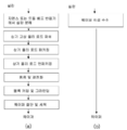
다결정 PV 셀(cells) 또는 SC 웨이퍼(wafers)는 수많은 제조 단계에서 초고순도 또는 높은 등급의 다결정 실리콘(폴리실리콘)으로 제조된다. SiO2 또는 석영(quartz)은 채굴되고, 대용량 노(furnace)에서 97 내지 99%의 순도를 가진 금속 실리콘(metallurgical grade silicon)으로 분해된다. 유동상 등급 실리콘은 실리콘 함유 가스로 변화되고, 상기 실리콘 함유 가스는 증류에 의해 정제된다. 실리콘 함유 가스는 지멘스 또는 유동상 반응기 공정을 통해 폴리실리콘을 제공될 수 있도록 분해된다. 지멘스 또는 유동상 반응기 공정에 의해 제조되는 물질은 결정립 실리콘 잉곳을 제조하기 위해 초크랄스키 공정(Czochralski process, 단결정질 제조) 또는 브리즈만-스톡바걸 공정(Bridgman-Stockbarger process, 다졀정질 제조)에서 용융되고 결정화된다. 상기 잉곳은 바람직한 웨이퍼 크기를 가진 브릭(brick)으로 절단된다. 상기 공정을 도 8a에 도식적으로 나타내었다.
Polycrystalline PV cells or SC wafers are made of ultra high purity or high grade polycrystalline silicon (polysilicon) in many manufacturing steps. SiO 2 or quartz is mined and decomposed into metallurgical grade silicon with a purity of 97 to 99% in large furnaces. Fluid bed grade silicon is converted to a silicon containing gas, which is purified by distillation. The silicon containing gas is decomposed to provide polysilicon through a Siemens or fluidized bed reactor process. Materials produced by the Siemens or fluidized bed reactor process are melted in the Czochralski process or the Brigman-Stockbarger process to produce grain silicon ingots. And crystallize. The ingot is cut into bricks having the desired wafer size. The process is shown schematically in FIG. 8A.
본 발명의 목적은 고상 멀티크리스탈라인 실리콘 잉곳 또는 웨이퍼의 제조방법을 제공하는 데 있다.It is an object of the present invention to provide a method for producing a solid multicrystalline silicon ingot or wafer.
또한, 본 발명의 다른 목적은 고상 멀티크리스탈라인 실리콘의 제조방법을 제공하는 데 있다.In addition, another object of the present invention to provide a method for producing a solid phase multi-crystalline silicon.
나아가, 본 발명의 또 다른 목적은 고상 멀티크리스탈라인 실리콘 생산물 시스템을 제공하는 데 있다.
Furthermore, another object of the present invention is to provide a solid state multicrystalline silicon product system.
상기 목적을 달성하기 위해, 본 발명은 반응 공간과 대면하는 내부면(i)과 반대되는 외부면(ii) 및 생산물 배출관을 가진 반응기 챔버벽을 포함하는 상기 반응기 챔버에 실리콘 함유 가스를 공급하는 단계; 상기 반응기 공간에 플라즈마를 발생시키는 단계; 액상 실리콘을 제조할 수 있는 충분한 온도에서 상기 실리콘 함유 가스를 노출시켜 상기 실리콘 함유 가스를 열적으로 분해시키는 단계; 상기 실리콘 함유 가스를 열적으로 분해시키는 동안 상기 반응기 챔버벽의 내부면을 실리콘의 녹는점 이하의 평형 온도로 유지시키는 단계; 및 상기 생산물 배출관으로부터 고상 멀티크리스탈라인 실리콘 잉곳 또는 웨이퍼로 주조하기 위한 모듈로 상기 액상 실리콘을 공급하는 단계를 포함하는 고상 멀티크리스탈라인 실리콘 잉곳 또는 웨이퍼의 제조방법을 제공한다.In order to achieve the above object, the present invention provides a step of supplying a silicon-containing gas to the reactor chamber comprising a reactor chamber wall having an outer surface (ii) opposite the inner surface (i) facing the reaction space and a product discharge pipe. ; Generating a plasma in the reactor space; Thermally decomposing the silicon containing gas by exposing the silicon containing gas at a temperature sufficient to produce liquid silicon; Maintaining the inner surface of the reactor chamber wall at an equilibrium temperature below the melting point of silicon while thermally decomposing the silicon containing gas; And supplying the liquid silicon to the module for casting into the solid state multicrystalline silicon ingot or wafer from the product discharge pipe.
또한, 본 발명은 반응 공간과 대면하는 내부면(i)과 반대되는 외부면(ii) 및 생산물 배출관을 가진 반응기 챔버에 실리콘 함유 가스를 공급하는 단계; 상기 반응기 공간에 플라즈마를 발생시키는 단계; 액상 실리콘을 제조할 수 있는 플라즈마에 상기 실리콘 함유 가스를 노출시켜 상기 반응기 공간에서 상기 실리콘 함유 가스를 열적으로 분해시키는 단계; 상기 실리콘 함유 가스를 열적으로 분해시키는 동안 상기 반응기 챔버벽의 내부면을 실리콘의 녹는점 이하의 평형 온도로 유지시키는 단계; 및 상기 생산물 배출관으로부터 고상 멀티크리스탈라인 실리콘으로 액상 실리콘을 직접 주조하는 단계를 포함하는 고상 멀티크리스탈라인 실리콘의 제조방법을 제공한다.The present invention also provides a method comprising the steps of: supplying a silicon-containing gas to a reactor chamber having an outer surface (ii) opposite the inner surface (i) facing the reaction space and a product discharge tube; Generating a plasma in the reactor space; Thermally decomposing the silicon containing gas in the reactor space by exposing the silicon containing gas to a plasma capable of producing liquid silicon; Maintaining the inner surface of the reactor chamber wall at an equilibrium temperature below the melting point of silicon while thermally decomposing the silicon containing gas; And directly casting liquid silicon from the product discharge pipe into solid multicrystal line silicon.
나아가, 본 발명은 실리콘 함유 가스 공급 주입관; 챔버 반응 공간을 한정하고, 반응 공간과 대면하는 내부면(i) 및 반대되는 외부면(ii)을 가진 반응기 챔버벽을 포함하는 반응 챔버; 상기 반응 챔버와 결합되고, 상기 챔버의 반응 공간내 열에너지를 발생시키도록 형성되는 플라즈마 에너지 소스; 상기 반응 챔버로부터 액상 실리콘을 배출하도록 형성되는 생산물 배출관; 및 상기 생산물 배출관과 함께 액상이 전달되고, 상기 액상 실리콘으로부터 고상 멀티크리스탈라인 실리콘을 직접적으로 생산하기 위해 형성되는 고형화 모듈을 포함하는 고상 멀티크리스탈라인 실리콘 생산물 시스템을 제공한다.
Furthermore, the present invention provides a silicon-containing gas supply injection tube; A reaction chamber defining a chamber reaction space and including a reactor chamber wall having an inner surface (i) facing the reaction space and an opposite outer surface (ii); A plasma energy source coupled with the reaction chamber and configured to generate thermal energy in the reaction space of the chamber; A product discharge pipe configured to discharge liquid silicon from the reaction chamber; And a solidification module in which a liquid phase is delivered together with the product discharge pipe and is formed to directly produce the solid phase multicrystalline silicon from the liquid silicon.
본 발명은 실리콘 함유 물질 또는 반응성 금속을 유용한 생산물 형태로 전환하기 위해 실리콘 함유 물질 또는 반응성 금속을 열적으로 처리하기 위한 방법을 제공한다. 예를 들어, 저등급, 루스팩(loose-packed), 고표면적 제품에서 태양전지로 제조하기 위한 적합한 실리콘 전구체 모양으로 실리콘 분말을 개선하는 방법을 제공한다. 열처리 공정 동안 오염되는 것을 방지하는 것은 순도, 특히 초고순도 제품을 얻기 위해 중요하다. 오염 요인 중 하나는 반응기 시스템을 구성하는 물질이다. 본 발명에 따른 장치, 시스템 및 방법에 따르면, 고상 실리콘 또는 고상 반응성 금속을 포함하는 스컬층(skull layer)은 상기 반응기의 내면의 적어도 일부분에서 형성된다. 상기 스컬층은 공급재와 반응기 시스템 표면 물질의 접촉을 방지하기 때문에 오염을 방지하거나 최소화한다. 또한, 상기 스컬층은 반응기 내벽 구성물질이 제조된 실리콘 제품으로 이동하는 것을 방지하는 확산 장벽(diffusion barrier)을 제공한다.
The present invention provides a method for thermally treating a silicon containing material or reactive metal to convert the silicon containing material or reactive metal into a useful product form. For example, there is provided a method for improving silicon powders into suitable silicon precursor shapes for solar cell manufacture in low grade, loose-packed, high surface area products. Preventing contamination during the heat treatment process is important for obtaining purity, especially ultra high purity products. One contaminant is the material that makes up the reactor system. According to the apparatus, system and method according to the invention, a skull layer comprising solid phase silicon or solid phase reactive metal is formed on at least a portion of the inner surface of the reactor. The skull layer prevents or minimizes contamination because it prevents contact between the feedstock and the reactor system surface material. The skull layer also provides a diffusion barrier that prevents reactor inner wall components from moving to the manufactured silicon product.
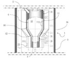
도 1a 및 1b는 본 발명에 따른 반응기 시스템의 일 실시예를 나타낸 것이다. 도 1a는 도 1b에서 나타낸 반응기의 벽 부분을 확대한 것이다.
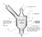
도 2는 본 발명에 따른 반응기 시스템의 또 다른 실시예를 나타낸 것이다.
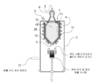
도 3은 고형화 일 실시예를 포함하는 반응기 시스템을 나타낸 것이다.
도 4는 또 다른 고형화를 포함하는 반응기 시스템을 나타낸 것이다.
도 5는 또 다른 고형화를 포함하는 반응기 시스템을 나타낸 것이다.
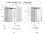
도 6은 본 발명에 따른 반응기 시스템에서 온도 구배를 나타낸 것이다.
도 7은 본 발명에 따른 반응기 시스템에서 두가지 열 흐름을 나타낸 것이다.
도 8a는 실리콘 웨이퍼를 제조하는 종래기술 단계를 도식적으로 나타낸 것이다.
도 8b는 본 발명의 제조방법에 따른 일 실시예를 도식적으로 나타낸 것이다. 1A and 1B show one embodiment of a reactor system according to the present invention. FIG. 1A is an enlarged view of the wall portion of the reactor shown in FIG. 1B.
2 shows another embodiment of a reactor system according to the invention.
3 shows a reactor system comprising one embodiment of solidification.
4 shows a reactor system including another solidification.
5 shows a reactor system including another solidification.
Figure 6 shows the temperature gradient in the reactor system according to the present invention.
Figure 7 shows two heat flows in a reactor system according to the present invention.
8A schematically illustrates a prior art step for fabricating a silicon wafer.
Figure 8b schematically shows an embodiment according to the manufacturing method of the present invention.
본 발명은 실리콘 함유 물질 또는 반응성 금속을 유용한 생산물 형태로 전환하기 위해 실리콘 함유 물질 또는 반응성 금속을 열적으로 처리하기 위한 방법을 제공한다. 예를 들어, 저등급, 루스팩(loose-packed), 고표면적 제품에서 광전지로 제조하기 위한 적합한 실리콘 전구체 모양으로 실리콘 분말을 개선하는 방법을 제공한다. 열처리 공정 동안 오염되는 것을 방지하는 것은 순도, 특히 초고순도 제품을 얻기 위해 중요하다. 오염 요인 중 하나는 반응기 시스템을 구성하는 물질이다. 본 발명에 따른 장치, 시스템 및 방법에 따르면, 고상 실리콘 또는 고상 반응성 금속을 포함하는 스컬층(skull layer)은 상기 반응기의 내면의 적어도 일부분에서 형성된다. 상기 스컬층은 공급 물질과 반응기 시스템 표면 물질의 접촉을 방지하기 때문에 오염을 방지하거나 최소화한다. 또한, 상기 스컬층은 반응기 내벽 구성물질이 제조된 실리콘 제품으로 이동하는 것을 방지하는 확산 장벽(diffusion barrier)을 제공한다. The present invention provides a method for thermally treating a silicon containing material or reactive metal to convert the silicon containing material or reactive metal into a useful product form. For example, there is provided a method for improving silicon powder into a suitable silicon precursor shape for photovoltaic production in low grade, loose-packed, high surface area products. Preventing contamination during the heat treatment process is important for obtaining purity, especially ultra high purity products. One contaminant is the material that makes up the reactor system. According to the apparatus, system and method according to the invention, a skull layer comprising solid phase silicon or solid phase reactive metal is formed on at least a portion of the inner surface of the reactor. The skull layer prevents or minimizes contamination because it prevents contact of the feed material with the reactor system surface material. The skull layer also provides a diffusion barrier that prevents reactor inner wall components from moving to the manufactured silicon product.
일 실시예에 따르면, 반응 공간과 직면하는 내부면(i)과 반대되는 외부면(ii)을 가진 반응기 챔버벽을 포함하는 반응기 챔버에 실리콘을 함유하는 원료 또는 반응성 금속 원료를 공급하는 단계;According to one embodiment, a method comprising: supplying a silicon-containing raw material or a reactive metal raw material to a reactor chamber comprising a reactor chamber wall having an outer surface (ii) opposite the inner surface (i) facing the reaction space;
액상 실리콘 생산물 또는 액상 반응성 금속 생산물을 충분하게 생산하기 위해 반응 공간내에 제1 열에너지를 발생시키는 단계;Generating first thermal energy in the reaction space to sufficiently produce a liquid silicon product or a liquid reactive metal product;
제2 열에너지로부터 상기 반응기 챔버벽의 외부면에 최초 열흐름을 부여하는 방식으로 상기 반응기 챔버벽으로 상기 제2 열에너지를 발생시키는 단계; 및 Generating the second thermal energy from the second thermal energy to the reactor chamber wall in a manner that imparts an initial heat flow to the outer surface of the reactor chamber wall; And
상기 제1 열어너지 소스와 상기 제2 열에너지 소스를 조절하여 상기 실리콘 또는 상기 반응성 금속의 녹는점 상하 온도 범위 내에서 내벽 표면 온도를 형성하는 단계를 포함하는 실리콘 또는 반응성 금속의 제조방법을 제공한다.It provides a method of producing a silicon or a reactive metal comprising the step of adjusting the first open source and the second thermal energy source to form the inner wall surface temperature within the melting point of the silicon or the reactive metal temperature range.
또한, 일 실시예에서, 반응 공간과 대면하는 내부면(i)과 반대되는 외부면(ii)을 가진 반응기 챔버벽을 포함하는 반응기 챔버에 실리콘 분말을 공급하는 단계;Further, in one embodiment, supplying silicon powder to a reactor chamber comprising a reactor chamber wall having an outer surface (ii) opposite the inner surface (i) facing the reaction space;
상기 반응기 공간에 플라즈마를 발생시키는 단계;Generating a plasma in the reactor space;
상기 플라즈마를 통해 실리콘 분말의 녹는점보다 높은 온도로 상기 실리콘 분말을 가열하여 상기 실리콘 분말을 열적으로 용융시켜 액상 실리콘을 제조하는 단계;Preparing liquid silicon by heating the silicon powder to a temperature higher than the melting point of the silicon powder through the plasma to thermally melt the silicon powder;
상기 실리콘 분말을 열적으로 용융시키는 동안 상기 반응기 챔버의 내부 표면벽을 상기 실리콘 분말의 녹는점 이하의 평형 온도로 유지시키는 단계; 및Maintaining the inner surface wall of the reactor chamber at an equilibrium temperature below the melting point of the silicon powder while thermally melting the silicon powder; And
상기 반응기 챔버에서 상기 액상 실리콘을 배출한 후 응고시키는 단계를 포함하는 실리콘의 제조방법을 제공한다. It provides a method for producing silicon comprising the step of solidifying after discharging the liquid silicon in the reactor chamber.
추가적인 일 실시예는, 반응 공간과 대면하는 내부면(i)과 반대되는 외부면(ii) 및 생산물 배출관을 가진 반응기 챔버벽을 포함하는 반응기 챔버에 실리콘 함유 가스를 공급하는 단계;A further embodiment includes supplying a silicon-containing gas to a reactor chamber including a reactor chamber wall having an exterior surface (ii) opposite the interior surface (i) facing the reaction space and a product discharge tube;
상기 반응기 공간에 플라즈마를 발생시키는 단계;Generating a plasma in the reactor space;
액상 실리콘을 제조할 수 있는 충분한 온도로 상기 실리콘 함유 가스를 가열하여 열적으로 분해시키는 단계;Thermally decomposing the silicon-containing gas to a temperature sufficient to produce liquid silicon;
상기 실리콘 함유 가스를 열적으로 분해시키는 동안 상기 반응기 챔버벽의 내부면을 실리콘의 녹는점 이하의 평형 온도로 유지시키는 단계; 및Maintaining the inner surface of the reactor chamber wall at an equilibrium temperature below the melting point of silicon while thermally decomposing the silicon containing gas; And
상기 생산물 배출관으로부터 고상 멀티크리스탈라인 실리콘 잉곳 또는 웨이퍼로 캐스팅하기 위한 모듈로 상기 액상 실리콘을 공급하는 단계를 포함하는 고상 멀티크리스탈라인 실리콘의 제조방법을 제공한다.It provides a method for producing a solid state multi-crystal line silicon comprising the step of supplying the liquid silicon to the module for casting from the product discharge pipe to a solid state multi-crystal line silicon ingot or wafer.
또한, 본 발명은 실리콘 함유 공급원료 또는 반응성 금속 공급원료;The present invention also provides a silicone containing feedstock or a reactive metal feedstock;
반응 공간과 직면하는 내부면(i)과 반대되는 외부면(ii)을 포함하고, 상기 챔버 반응기 공간을 한정하는 반응기 챔버벽을 포함하는 반응기 챔버;A reactor chamber comprising an outer surface (ii) opposed to an inner surface (i) facing the reaction space and comprising a reactor chamber wall defining the chamber reactor space;
상기 반응기 챔버와 결합되고 상기 챔버 반응기 공간 내에 열에너지를 공급하기 위해 구비되는 플라즈마 에너지 소스;A plasma energy source coupled to the reactor chamber and provided for supplying thermal energy within the chamber reactor space;
상기 반응기 챔버 벽의 외부면에 열을 가하기 위해 형성되고, 상기 반응기 챔버의 외부에 구비되는 외부 열에너지 소스; 및An external heat energy source formed to apply heat to an outer surface of the reactor chamber wall and provided outside the reactor chamber; And
상기 반응기 챔버로부터 액상 실리콘 또는 액상 반응성 금속을 배출하기 위해 형성되는 생산물 배출관을 포함하는 반응기 시스템을 제공한다. It provides a reactor system comprising a product discharge pipe formed to discharge liquid silicon or liquid reactive metal from the reactor chamber.
이하, 본 발명을 첨부된 도면을 참조하여 상세히 설명한다.Hereinafter, with reference to the accompanying drawings the present invention will be described in detail.
"a", "an", 및 "the" 방식의 단칭 용어는 다른 방법으로 문맥에서 분명하게 나타내지 않는 경우에는 다수의 지시대상을 포함한다. "구성하다(comprises)"는 "포함한다(includes)"를 나타낸다. 다른 방법으로 나타내지 않으면, 화학적 명명에 의한 구성요소에 대한 설명은 기술에서 명기한 어떠한 조합에 추가되는 구성요소를 나타내고, 혼합된 혼합물의 구성요소들 중 화학적 상호작용을 필수적으로 제외하지는 않는다. 여기서 언급된 어떤 수치는 하한값과 상한값 사이의 적어도 2 단위가 분리된다면 1 단위 증가로 하한값으로부터 상한값까지 모든 값을 포함한다. 예를 들어, 구성요소의 양 또는 공정변수 값이 1에서부터 90까지, 바람직하게는 20에서부터 80까지, 더욱 바람직하게는 30에서부터 70까지로 명시되면 15에서 85까지, 22에서 68까지, 43에서 51까지, 30에서 32까지 등과 같은 값은 본 발명에서 명백하게 열거되는 것을 의미한다. 1 단위 차이보다 적은 값에 있어서, 1 단위는 적절하게 0.1, 0.01, 0.001 또는 0.0001로 고려된다. 여기에서 열거되는 가장 낮은 값과 높은 값 사이인 수치의 모든 가능한 조합들은 본 발명에서 명백하게 언급한다.The term “a”, “an”, and “the” are intended to include a number of referents unless the context clearly indicates otherwise. "Comprises" refers to "includes". Unless indicated otherwise, descriptions of components by chemical nomenclature refer to components added to any combination specified in the description and do not necessarily exclude chemical interactions among the components of the mixed mixture. Any number referred to herein includes all values from the lower limit to the upper limit in one unit increments if at least two units are separated between the lower limit and the upper limit. For example, if the quantity or process variable value of a component is specified from 1 to 90, preferably from 20 to 80, more preferably from 30 to 70, from 15 to 85, from 22 to 68, from 43 to 51 , Values such as 30 to 32, etc., are meant to be explicitly listed in the present invention. For values less than one unit difference, one unit is considered to be 0.1, 0.01, 0.001 or 0.0001 as appropriate. All possible combinations of numerical values between the lowest and highest values enumerated herein are expressly mentioned in the present invention.
본 발명에서, "멀티크리스탈라인(multicrystalline)" 실리콘은 "폴리크리스탈라인(polycrystalline)" 실리콘(폴리크리스탈라인 실리콘은 "폴리실리콘"으로 언급된다)의 미세구조와 비교하여 서로 다른 미세구조를 나타낸다. 폴리크리스탈라인 실리콘의 미세구조는 상기에서 기술한 지멘스 공정 또는 유동상 반응기 공정으로 제조된 생산물이다. 폴리크리스탈라인 실리콘은 종래의 브리즈만-스톡바걸 공정에서 멀티크리스탈라인 실리콘 잉곳 또는 종래의 초크랄스키 공정에서 모노크리스탈라인 실리콘 잉곳을 생산하기 위한 공급원료이다. 멀티크리스탈라인 실리콘 구조는 액상 실리콘의 방향성 고체화의 결과이다. 일반적으로, 폴리크리스탈라인 실리콘의 미세구조는 각각의 작은 결정으로 이루어지고, 기상으로부터 실리콘층 성장의 결과이다. 멀티크리스탈라인 실리콘(multicrystalline)은 한방향으로 배열되고 용융된 실리콘이 1차원 온도 구배 하에서 고형화될 때 제조되는 큰 결정으로 이루어진다. In the present invention, "multicrystalline" silicon exhibits different microstructures compared to the microstructures of "polycrystalline" silicon (polycrystalline silicon is referred to as "polysilicon"). The microstructure of polycrystal silicon is the product produced by the Siemens process or fluidized bed reactor process described above. Polycrystalline silicon is a feedstock for producing multicrystalline silicon ingots in a conventional Brisman-Stockbargirl process or monocrystalline silicon ingots in a conventional Czochralski process. Multicrystalline silicon structures are the result of directional solidification of liquid silicon. In general, the microstructure of polycrystalline silicon consists of small crystals of each and is the result of silicon layer growth from the gas phase. Multicrystalline silicon (multicrystalline) consists of large crystals that are arranged in one direction and are produced when the molten silicon solidifies under a one-dimensional temperature gradient.
기술한 직접 주조법에 따라, 액상 실리콘은 제조된 실리콘 웨이퍼와 동일한 두께의 실리콘층으로 만들어질 수 있다. 상기 방법은 실리콘이 고형화되는 주조 유닛으로 액상 실리콘의 초고순도 또는 고등급 증기(예를 들어, 전자용(electronic grade) 또는 태양전지용(solar grade))를 직접적으로 공급한다. 상기에서 기술한 방법에서, 실리콘 함유 가스는 일체형 제조유닛 또는 모듈내에서 통합된 하나의 공정에서 실리콘 웨이퍼 또는 잉곳(액상 실리콘을 통해)으로 만들어진다. 예를 들어, 공정은 밀봉하여 기밀된 하나의 용기 챔버내에서 수행될 수 있다(도 3 참조). 도 8은 다단계로 이루어진 종래 방법을 회피하는 방법을 도식적으로 나타내었다. 본 발명은 실리콘을 재용융(재용융은 필수적으로 오염을 야기한다)시키지 않고, 이는 8 내지 25 kW/㎏의 실리콘이 절약될 수 있다. 상기에서 기술한 웨이퍼의 직접 주조 방법은 웨이퍼를 잘라내는 재료의 손실을 피할 수 있고, 웨이퍼를 제조하기 위해 필요한 에너지를 감소할 수 있다. 예를 들어, 종래 커팅 공정은 멀티크리스탈라인 실리콘 잉곳의 약 60%까지 작업폐기물로 손실된다. According to the direct casting method described, the liquid silicon can be made of a silicon layer of the same thickness as the silicon wafer produced. The method directly feeds ultra high purity or high grade vapor (eg, electronic grade or solar grade) of liquid silicon to the casting unit where the silicon is solidified. In the method described above, the silicon-containing gas is made into a silicon wafer or ingot (via liquid silicon) in one process integrated within an integrated manufacturing unit or module. For example, the process may be performed in one sealed chamber that is hermetically sealed (see FIG. 3). 8 diagrammatically shows a method of avoiding a multi-step conventional method. The present invention does not remelt the silicon (remelting necessarily causes contamination), which can save 8 to 25 kW / kg of silicon. The above-described direct casting method of the wafer can avoid the loss of material that cuts the wafer and can reduce the energy required to manufacture the wafer. For example, conventional cutting processes lose up to about 60% of the multicrystalline silicon ingot to work waste.
본 발명에 따른 반응기 시스템은 반응기 챔버벽의 내부면으로 공급되는 실리콘 또는 반응성 금속의 고상 스컬층을 유지하도록 설계된다. 또한, 상기 시스템의 설계는 상기 스컬층 두께를 정확하게 제어할 수 있도록 한다. 상기 스컬층은 내부 벽 표면의 일부분을 덮거나 내부 표면 전체를 덮을 수 있다. 상기 반응기 챔버벽의 내부면에서 고상 스컬층의 형성은 액상 실리콘 또는 액상 반응성 금속에 의해 챔버벽 구조물질이 부식되는 것을 보호하게 한다. 바꾸어 말하면, 상기 스컬층은 상기 챔버벽과 액상 실리콘 사이에 직접적인 접촉을 막고, 따라서 상기 액상 실리콘 생산물의 오염을 최소화한다. 상기 스컬층은 실리콘의 녹는점 또는 반응성 금속의 녹는점 이하의 온도에서 상기 반응기 챔버의 내부 표면을 유지함으로써 형성된다. The reactor system according to the invention is designed to maintain a solid skull layer of silicon or reactive metal which is fed to the inner surface of the reactor chamber wall. In addition, the design of the system allows precise control of the skull layer thickness. The skull layer may cover a portion of the inner wall surface or may cover the entire inner surface. The formation of a solid skull layer on the inner surface of the reactor chamber wall protects the chamber wall structural material from corrosion by liquid silicon or liquid reactive metal. In other words, the skull layer prevents direct contact between the chamber wall and liquid silicon, thus minimizing contamination of the liquid silicon product. The skull layer is formed by maintaining the inner surface of the reactor chamber at a temperature below the melting point of silicon or the melting point of the reactive metal.
상기 열 제어 시스템(thermal control system)은 상기 반응기 챔버 내부의 내부 열에너지 소스와 상기 반응기 챔버 바깥쪽 또는 외부에 위치한 외부 열에너지 소스의 조합을 포함한다. 상기 외부 열에너지 소스는 상기 반응기 챔버를 둘러싸는 용기 챔버(confinement chamber) 내에 위치한다. 상기 외부 열에너지 소스는 유도 가열(induction heating), 저항 가열(resistance heating) 또는 둘의 조합을 통해 상기 반응기 벽의 외부면으로 직접적으로 열을 공급할 수 있다. 도 1a,1b, 3 및 7b에서 나타낸 일 실시예에서 상기 외부 에너지 소스는 유도 코일이다. 도 2에 나타낸 또 다른 실시예에서 상기 외부 에너지 소스는 저항 가열기이다. 마이크로파는 또 다른 외부 에너지 소스일 수 있다. 상기 내부 에너지 소스는 하기에서 더욱 자세히 기술되는 바와 같이 플라즈마일 수 있다. 또 다른 방법으로, 상기 내부 에너지 소스는 전자빔, 저항 가열 요소 또는 유도 가열 요소일 수 있다. The thermal control system includes a combination of an internal heat energy source inside the reactor chamber and an external heat energy source located outside or outside the reactor chamber. The external heat energy source is located in a confinement chamber surrounding the reactor chamber. The external heat energy source may supply heat directly to the outer surface of the reactor wall through induction heating, resistance heating or a combination of both. In one embodiment shown in FIGS. 1A, 1B, 3 and 7B the external energy source is an induction coil. In another embodiment, shown in FIG. 2, the external energy source is a resistance heater. The microwave may be another external energy source. The internal energy source may be a plasma as described in more detail below. Alternatively, the internal energy source can be an electron beam, resistive heating element or induction heating element.
상기 내부 열에너지 소스와 외부 열에너지 소스에 의해 발생되는 열 흐름을 각각 도 7a 및 7b에 나타내었다. 상기 내부 열 흐름은 다음과 같이 진행한다: 가열된 반응가스→액상 실리콘 필름→고상 실리콘 스컬층→반응기 챔버벽. 상기 외부 열 흐름은 다음과 같이 진행한다: 반응기 챔버벽→고상 실리콘 스컬층→액상 실리콘 필름. 상기 내부 열에너지 소스는 공급 원료 물질의 열적 분해를 위한 에너지를 제공한다. 상기 외부 열에너지 소스는 실리콘 또는 반응성 금속의 녹는점에 근접한 범위(녹는점 아래)에서 상기 반응기 챔버 벽의 내부 온도를 정확하게 제어하는 수단을 제공한다. 나타나는 온도 구배는 도 6에 나타내었다. The heat flow generated by the internal and external thermal energy sources is shown in FIGS. 7A and 7B, respectively. The internal heat flow proceeds as follows: heated reactant gas → liquid silicon film → solid silicon skull layer → reactor chamber wall. The external heat flow proceeds as follows: reactor chamber wall → solid silicon skull layer → liquid silicon film. The internal thermal energy source provides energy for thermal decomposition of the feedstock material. The external thermal energy source provides a means for accurately controlling the internal temperature of the reactor chamber wall in the range close to the melting point (below the melting point) of the silicon or reactive metal. The resulting temperature gradient is shown in FIG. 6.
상기 외부 열에너지 소스는 적어도 하나의 온도 제어존(temperature control zone)을 형성할 수 있다. 서로 다른 온도 제어존은 서로 다른 온도 프로파일(profile) 또는 상기 반응기 챔버 축 길이에 따른 존을 형성하는데 이용될 수 있다. The external heat energy source may form at least one temperature control zone. Different temperature control zones may be used to form zones along different temperature profiles or the length of the reactor chamber axis.
상기에서 기술한 바와 같이, 기술한 공정은 도 6에 나타난 바와 같이 상기 반응기 챔버의 외부면에서 상기 반응기 챔버의 반응 공간까지 온도 구배를 형성한다. 구체적인 온도 구배는 공급 원료, 공급 속도, 상기 반응기 공간내 작동 압력 등을 포함하는 몇몇의 요소들에 좌우되어 변화될 것이다. 또한, 상기 온도 구배는 상기 반응기의 개시(start-up)에서부터 평형상태(steady-state)까지 변화하기 때문에 시간에 좌우된다. 반면, 일반적으로 상기 반응기 챔버벽의 내부면은 상기 공급 원료 물질의 녹는점 이하인 1 내지 300 ℃일 수 있고 바람직하게는 상기 공급 원료 물질의 녹는점 이하인 1 내지 100 ℃일 수 있고; 상기 스컬층은 상기 공급 원료 물질의 녹는점 이하인 300 ℃까지 공급 원료 물질의 녹는점일 수 있고 더욱 바람직하게는 녹는점 이하인 100 ℃까지 녹는점일 수 있으며; 상기 반응기 공간은 5,000 ℃ 이상까지 실리콘 또는 반응성 금속의 녹는점일 수 있다. As described above, the described process forms a temperature gradient from the outer surface of the reactor chamber to the reaction space of the reactor chamber as shown in FIG. 6. The specific temperature gradient will vary depending on several factors including feedstock, feed rate, operating pressure in the reactor space and the like. The temperature gradient also depends on time since it varies from start-up of the reactor to steady-state. On the other hand, in general, the inner surface of the reactor chamber wall may be 1 to 300 ° C. which is below the melting point of the feedstock material and preferably 1 to 100 ° C. which is below the melting point of the feedstock material; The skull layer may be a melting point of the feedstock material up to 300 ° C. which is below the melting point of the feedstock material, and more preferably, may be a melting point up to 100 ° C that is below the melting point; The reactor space may be the melting point of silicon or reactive metal up to 5,000 ° C. or more.
상기 전체적인 열 제어 접근법은 또한 하기에서 상세히 기술하는 바와 같이 절연(thermal insulation)을 포함할 수 있다. The overall thermal control approach may also include thermal insulation, as described in detail below.
상기 반응기 시스템의 실시예를 도 1 내지 5에 나타내었다. 일반적으로, 반응기 시스템(1)은 적어도 하나의 공급 원료 주입구(2), 적어도 하나의 액상 생산물 배출구(3), 반응기 챔버(4), 외부 오염 챔버(5) 및 플라즈마 발생 소스(6)를 포함한다. Examples of such reactor systems are shown in FIGS. Generally,
공급 원료 주입구(2)는 상기 반응기 챔버(4)로 공급원료의 공급을 제어할 수 있는 포트(port) 또는 밸브(valve) 형태일 수 있다. 예를 들어, 상기 주입구(2)는 석영(quartz), 흑연(graphite) 및/또는 실리콘으로 만들어진 수냉 구조(water cooled structure)의 노즐(nozzle)일 수 있다. The
상기 반응기 챔버(4)는 상기 반응기 챔버벽(10) 내 위치한 반응기 공간(13)으로 한정되는 반응기 챔버벽(10)을 포함한다. 상기 반응기 챔버벽(10)은 상기 반응기 공간(13)을 대면하는 내부면(11)과 반대되는 외부면(12)을 포함한다. 상기 반응기 챔버는 원통형, 타원형, 사각형 등과 같은 어떠한 모양으로 제공될 수 있다. 특정 실시예에서, 상기 반응기 챔버는 몇몇의 서로 다른 크기 및/또는 서로 다른 형상 부분을 가질 수 있다. 예를 들어, 도 1은 제1 원통형 부분(14)과, 제2 테이퍼드(tapered) 부분 또는 원뿔형 부분(15)을 나타낸다. 제2 부분(15)은 상기 생산물 배출관(3)으로 점점 가늘어진다. 상기 반응기 챔버벽(10)은 공급 원료 또는 생산물의 부식 및 오염을 저지하고 스컬층을 형성할 수 있고 열 또는 에너지를 전달하거나 방해하는 특성을 제공하는 어떠한 물질로도 만들 수 있다. 벽 구조 물질의 일례로 흑연, 몰리브데늄, 텅스텐, 티타늄, 세라믹(예를 들어, 알루미나) 및 석영을 포함한다. The
상기 내부면(11) 영역은 내부면(11)에서 공급 원료 물질의 수집과 액상 변화가 가능하도록 충분히 커야만 한다. ㎏/h로 나타나는 바람직한 처리량에 좌우되어 상기 내부면(11) 영역은 1 내지 50 ㎏/h 범위의 생산물 처리량을 위해 0.2 내지 5 ㎡의 범위여야 한다. The
플라즈마 발생을 위한 전력공급은 다양한 유형일 수 있다. 플라즈마의 일례는 RF, DC arc 또는 마이크로파 플라즈마를 포함한다. 특정 플라즈마 유형에 의존하여 상기 플라즈마 파워는 1 내지 1000 ㎾ 범위일 수 있고, 더욱 바람직하게는 10 내지 200 ㎾ 범위일 수 있다. The power supply for plasma generation can be of various types. Examples of plasmas include RF, DC arc or microwave plasma. Depending on the particular plasma type, the plasma power may range from 1 to 1000 kW, more preferably from 10 to 200 kW.
상기 생산물 배출관(3)은 생산물 수집 모듈 및/또는 생산물 고형 모듈과 연결될 수 있다. 예를 들어, 생산물은 고형화 타워(solidification tower)를 통해 자유낙하하는 동안 냉각된 후 ㎜ 크기의 액적(droplet)이라면 빈(bin)에 수집될 수 있다. 0.5 ㎜의 직경을 가진 액적은 고형화되고, 약 6 내지 8 미터의 거리를 통과하여 낙하한 후 약 600 ℃의 온도까지 냉각된다. 상기 온도에서 고형화된 실리콘 액적은 물로 냉각될 수 있는 생산물 수집 빈에 수집될 수 있다. 대안으로 액적을 추가적으로 냉각하기 위해 자유낙하 높이를 증가시킬 수 있고 수냉각 없이 빈에 상기 실리콘 생산물을 수집할 수 있다. The
도 1a와 1b의 실시예에서, 적어도 하나의 열 유도 코일(20)은 상기 반응기 챔버 벽의 외부면(12) 또는 외부면 근처에 위치한다. 상기 코일(20)은 상기 반응기 챔버의 둘레 모두 또는 둘레 일부를 둘러쌀 수 있다. 상기 코일(20)은 상기 반응기 챔버 벽을 충분히 가열할 수 있는 다양한 열 전달 물질로 만들 수 있다. 또한, 상기 코일(20)은 히트싱크(heat sink)로 작용할 수 있고, 히트싱크로 작용하는 수냉 외부 용기 챔버벽을 보충할 수 있다. In the embodiment of FIGS. 1A and 1B, at least one
도 2의 일 실시예에서, 적어도 하나의 히터(21)는 상기 반응기 챔버벽의 외부면(12) 또는 외부면 근처에 배치된다. 상기 저항성 히터(21)는 상기 반응기 챔버벽을 가열한다. 또한, 도 2의 일 실시예는 상기 반응기 챔버벽과 용기 챔버벽 사이에 구비되는 절연 요소(22)를 포함한다. 상기 절연 두께는 상기 반응기 수직축에 따라 상이한 두께를 가지게 고안될 수 있다. In one embodiment of FIG. 2, at least one
또 다른 일 실시예에서(미도시), 상기 반응기 챔버를 위한 외부 열에너지 소스는 제공되지 않는다. 다시 말해서, 상기 반응기 공간 내 열에너지를 발생시키기 위한 열에너지 소스만이 존재한다.In another embodiment (not shown), no external heat energy source for the reactor chamber is provided. In other words, there is only a heat energy source for generating heat energy in the reactor space.
예를 들어, 상기 외부 용기 챔버(5)는 도 2 및 3에 나타난다. 상기 용기 챔버(5)는 적어도 하나의 상기 반응기 챔버(4)에 밀봉하여 밀폐된다. 상기 용기 챔버(5)는 물로 냉각될 수 있는 용기 챔버벽(16)을 포함한다. 또한, 상기 수냉 용기 챔버(16)는 상기에서 기술한 바와 같이 상기 반응기 챔버의 열에너지 및 열 흐름을 위한 히트싱크일 수 있다. For example, the
도 3 내지 5는 상기 반응기 시스템과 결합할 수 있는 다수의 고형화 모듈을 나타낸다. 3 to 5 show a number of solidification modules that can be combined with the reactor system.
도 3은 실리콘 잉곳을 캐스팅할 수 있는 연속 주조 시스템과 결합된 전자기 도가니(electromagnetic crucible)를 포함한다. 도 4는 직접적으로 고형화된 실리콘 잉곳을 생산하기 위한 형상을 나타낸다. 액상 실리콘은 상기 배출관(3)으로부터 전자기 도가니로 흐를 수 있다. 직접적으로 결합된 전자기 주조의 이점은 이송용기를 위한 추가적인 비용이 들지 않고 실리콘이 재용융되지 않으며, 고순도 실리콘이 스컬층이 없는 도가니에서 고형되기 때문에 오염이 최소화된다. 도 5는 본 발명에 따른 반응기 시스템의 액상 생산물을 수평 이동 지지 기판(27)으로 공급함으로써 직접적인 웨이퍼 주조가 가능한 형상을 나타낸다. 지지 기판(27)을 위한 물질의 일례로 실리콘 카바이드, 실리콘 나이트라이드, 알루미늄 옥사이드, 지르코늄 옥사이드 또는 멀라이트(mullite)를 들 수 있다. 미국 특허번호 4,670,096호에는 수평 이동 지지체에서 액상 실리콘으로 직접적인 웨이퍼 주조에 대한 공정이 기재되어 있다. 3 includes an electromagnetic crucible coupled with a continuous casting system capable of casting a silicon ingot. 4 shows a shape for producing a directly solidified silicon ingot. Liquid silicon can flow from the
더욱 상세하게, 도 3 및 4는 물로 냉각될 수 있는 전자기 주조 도가니(41)의 상부 가열을 위한 적어도 하나의 유도 코일(40)을 나타낸다. 상기 유도 코일(40)은 잉곳을 회수하는 동안 상기 스컬층을 파괴하기 위해 1 ㎜ 두께 이하로 상기 스컬층을 용융하는데 사용될 수 있다. 상기 액상 실리콘은 새로운 스컬층으로 형성될 것이다. 도가니에서 스컬층 형성 및 파괴 사이클은 필요한 만큼 반복될 수 있다. 상기 잉곳은 증가 단계에서 회수될 수 있다. 전자기 주조 도가니의 예는 EP1154047호에 기재되어 있다. 도 3은 또한 배기 가스 처리 시스템에 연결되는 배기 가스부(23)를 포함한다. More specifically, FIGS. 3 and 4 show at least one induction coil 40 for top heating of an electromagnetic casting crucible 41 that can be cooled with water. The induction coil 40 may be used to melt the skull layer to less than 1 mm thick to break the skull layer during ingot recovery. The liquid silicon will be formed of a new skull layer. In the crucible, the skull layer forming and breaking cycle can be repeated as necessary. The ingot can be recovered in an incremental step. Examples of electromagnetic casting crucibles are described in EP1154047. 3 also includes an
더욱 상세하게, 도 5는 상기 액상 생산물 배출관(3)이 몰딩 요소의 형태로 형성되는 도안을 나타낸다. 상기 액상 생산물 배출관의 출구에서 내부 단면의 치수와 구멍 모양은 액상 실리콘의 생산물 증기가 수평 지지 기판(27)으로 유동하기 위한 바람직한 모양 및 치수이다. 예를 들어, 상기 액상 생산물 배출관의 출구 표면은 상기 수평 지지 기판(27)의 면에 대하여 각이 있거나 가늘어질 수 있다. 상기 액상 생산물 배출관 구조는 축방향 자유 이동뿐만 아니라 기울어진 이동을 허용하도록 형성될 수 있다. 후가열기(after-heater)는 일방향으로 고형화되게 하고 평평한 웨이퍼 표면이 제조되도록 상기 액상 생산물 배출관(3)의 하부에 위치할 수 있다. In more detail, FIG. 5 shows a design in which the
상기 액상 실리콘이 상기 지지 기판(27) 물질과 접촉할 때, 상기 지지체(27) 온도가 실리콘의 녹는점 이하이면, 고형화된 멀티크리스탈라인 실리콘(예를 들어, 실리콘 포일(foil))이 형성될 것이다. 상기 고형화된 층은 상기 액상과의 접촉이 유지되는 한 상기 생산물 배출관(3)과 후가열기 하에서 전진 이동 동안 지지체의 밑면으로부터 열을 제거하여 성장을 지속적으로 할 수 있다. 동적 평형 상태에서, 생산물 배출관(3)의 길이에 상응하는 성장 웨지(growth wedge)는 형성될 것이다. When the liquid silicon is in contact with the support substrate 27 material, if the support 27 temperature is below the melting point of the silicon, solidified multicrystalline silicon (for example, silicon foil) is formed. will be. The solidified layer can continue to grow by removing heat from the underside of the support during the forward movement under the
잉곳의 직접 주조에 대한 또 다른 일 실시예에 따르면, 상기 액상 실리콘은 전체적인 참조로 본 발명에서 통합되는 미국 특허번호 4,936,375호에 나타낸 것과 유사한 연속 주조 도가니 모듈로 직접적으로 공급될 수 있다. 상기 실시예에서 베드는 상기 액상 생산물 배출관(3) 밑에 위치한다. 상기 베드는 상기 배출관(3)으로부터 액상 실리콘을 수용하기 위한 캐비티(cavity)로 한정한다. 액상 실리콘의 풀(pool)은 상기 베드 캐비티에 형성된다. 흐름 채널(flow channel)은 베드 벽 개구(opening)에 의해 형성되고, 몰드에서 파이프를 통해 순환된 액체를 냉각시킨 결과로 상기 풀로부터 실리콘이 잉곳으로 고형화되는 몰드로 상기 액상 실리콘의 증기가 흐르게 한다. 균일한 결정구조를 제공하기 위해 상기 잉곳은 상기 몰드로부터 아래방향으로 흐르고, 상기 잉곳은 흐름 채널을 통해 몰드로 액상 실리콘을 공급하는 속도에 따라 균일한 속도에서 연속적으로 흐르게 하여야 한다. 또 다른 실시예에서, 상기 액상 생산물 배출관(3)으로부터 액상 실리콘은 베드 캐비티로 들어가지 않고 몰드에서 직접적으로 공급될 수 있다. According to another embodiment for direct casting of ingots, the liquid silicone can be supplied directly to a continuous casting crucible module similar to that shown in US Pat. No. 4,936,375, incorporated herein by reference in its entirety. In this embodiment a bed is situated below the
웨이퍼 또는 실리콘 스트립의 직접 주조를 위한 또 다른 실시예에 따르면 상기 액상 실리콘은 전체적으로 참조로 통합되는 미국특허 4,212,343호에 나타난 것과 유사한 모듈로 직접적으로 공급될 수 있다. 상기 실시예에서, 연속적인 얇은 실리콘 스트립은 칠바디(chill body)의 표면에 근접하게 위치하는 슬롯형 노즐을 통해 압력하에서 이동 칠바디의 표면으로 상기 액상 실리콘을 밀어 넣음으로써 형성될 수 있다. 이동 칠 표면에서 실리콘 리본을 형성하기 위한 추가적인 모듈은 전체적으로 참조로 통합되는 미국특허 4,274,473호에 나타난다. According to another embodiment for direct casting of a wafer or silicon strip, the liquid silicon can be supplied directly to a module similar to that shown in US Pat. No. 4,212,343, which is incorporated by reference in its entirety. In this embodiment, a continuous thin silicon strip can be formed by forcing the liquid silicon under pressure through a slotted nozzle positioned proximate the surface of the chill body to the surface of the moving chill body. Additional modules for forming a silicone ribbon on a moving fill surface are shown in US Pat. No. 4,274,473, which is incorporated by reference in its entirety.
상기 반응기 시스템의 작동은 상기 공급 원료 물질의 녹는점보다 높은 온도로 상기 반응기 챔버벽(외부열 소스, 내부열 소스 또는 상기 외부열과 내부열 소스의 결합으로부터 열에너지를 통해)을 가열하여 시작할 수 있다. 실리콘을 함유하는 물질로 전가열하는 것은 흑연 반응기 챔버벽에서 실리콘 카바이드층을 형성하게 한다. 상기 반응기 챔버벽의 온도는 낮아질 것이고, 따라서 내부면은 상기 공급 연료 물질의 녹는점 이하가 될 것이다. 상기 반응기 공간(13)에서 물질의 용융은 상기 내부면과 접촉할 것이고 고상(냉각된) 스컬층(17)의 형성을 시작할 것이다. 상기 스컬층(17)은 내부면(18)과 접촉면과 반대되는 벽(19)을 포함한다. 온도 구배는 도 6에 나타낸 상기 반응 공간에서 상기 반응기 챔버벽, 상기 스컬층 및 가스를 거쳐 형성된다. 열평형상태에서, 상기 스컬층의 두께는 더 이상 증가하지 않으며, 상기 스컬층 온도는 상기 반응기의 반응 공간(13)을 대면하는 면(18)에서 액상 물질 온도로 도달된다. 상기 액상 실리콘 필름(18)은 내부면(18)에서 응축되고, 그 후 상기 반응기 챔버의 수직 축 아래로 내부면(18)을 따라 흐르게 된다. 또한 상기 용융 공정은 실리콘 증기를 생산할 수 있다. Operation of the reactor system may begin by heating the reactor chamber wall (through heat energy from an external heat source, an internal heat source or a combination of the external and internal heat sources) to a temperature above the melting point of the feedstock material. Preheating with a material containing silicon causes the silicon carbide layer to form on the graphite reactor chamber walls. The temperature of the reactor chamber wall will be lowered so that the inner surface will be below the melting point of the feed fuel material. Melting of the material in the
실리콘 함유 원료 물질인 경우, 챔버벽 내부면(11)의 최대 온도는 스컬층 형성과 정상상태 동안 1414 ℃(실리콘의 녹는점보다 1 ℃ 낮음)를 초과하지 말아야 한다. 특정 실시예에서, 상기 내부면(11) 온도는 1115 내지 1414 ℃ 범위이고, 더욱 바람직하게는 1215 내지 1414 ℃ 범위이다. 상기 외부 열에너지 소스로부터의 열은 벽 온도를 조절하여 상기 스컬의 두께를 조절하는 것을 가능하게 하는 온도범위에서 상기 반응기 챔버벽의 온도를 유지한다. In the case of a silicon-containing raw material, the maximum temperature of the chamber wall
상기 반응기 챔버에서의 열 흐름은 일반적으로 상기 반응기 챔버 외부로 히트 싱크를 분산시킨다. 상기 히트 싱크는 단열과 같은 능동 냉각(예를 들어, 수냉 용기 챔버벽) 및/또는 수동 냉각일 수 있다. Heat flow in the reactor chamber generally disperses the heat sink outside the reactor chamber. The heat sink may be active cooling (eg, water cooled vessel chamber walls) and / or passive cooling such as thermal insulation.
상기 공급 원료 물질은 상기 입구(2)를 통해 상기 반응기 챔버(4)로 공급된다. 상기 공급 원료 물질은 실리콘 함유 물질 또는 반응성 금속일 수 있다. 상기 실리콘 함유 물질은 실리콘 분말 또는 미분말(fine), 또는 실란, 디실란, 고차 실란(SinH2n +2), 디클로로실란, 트리클로로실란, 실리콘 테트라클로라이드, 디브로모실란(dibromosilane), 트리브로모실란, 실리콘 테트라브로마이드(tetrabromide), 디아이오도실란(diiodosilane), 트리아이오도실란, 실리콘 테트라아이오디드(silicon tetraiodide) 또는 이들의 혼합물과 같은 실리콘을 함유하는 가스일 수 있다. 티타늄 또는 지르코늄과 같은 반응성 금속은 본 발명에 따른 공정 및 기계를 이용하여 환원될 수 있다. 상기 반응기 시스템으로 공급되는 실리콘 분말은 실리콘 핸들링(silicon handling, 예를 들어 파쇄(breaking), 연마(grinding) 또는 커팅(cutting)) 또는 실리콘 함유 가스를 분해하는 어떠한 공정에 의해 제공되는 실리콘 소입자(미분말/분말)일 수 있다. 상기 분말은 상기 반응기 시스템으로 주입되기 위해 캐리어 매질에서 분산시키거나 부유시킬 수 있다. 예를 들어, 상기 캐리어 매질은 실리콘 비활성 및/또는 Ar과 같은 이온화 퍼텐셜이 비교적 낮은 가스일 수 있다. The feedstock material is fed to the
상기 반응기 공간에서 작동 압력은 0.1 내지 2.0 bar 범위일 수 있고, 더욱 바람직하게는 0.5 내지 2.0 bar 범위일 수 있다. The operating pressure in the reactor space may range from 0.1 to 2.0 bar, more preferably from 0.5 to 2.0 bar.
상기 공급 원료 물질이 실리콘 함유 가스인 경우에는 가스가 액체로 변화하는 온도에서 임계온도는 열분해 온도이다. 따라서, 상기 반응기 챔버벽의 내면은 녹는점 아래의 온도에서 평형 온도를 유지한다. 도 4 및 5에 나타낸 실시예는 실리콘 함유 가스(예를 들어, 실란)으로부터 직접적으로 실리콘 잉곳(도 4) 또는 웨이퍼(도 5)를 제조할 수 있고, 따라서 값비싼 공정을 피할 수 있고 폴리크리스탈라인 실리콘의 재용융 및 커팅을 피할 수 있다. 할로겐, 제2 가스는 상기 반응기 공간(13)에서 실리콘 함유 가스와 함께 존재한다. 상기 할로겐은 SiH4가 Si와 할로겐으로 열분해된 결과이다. When the feedstock material is a silicon containing gas, the critical temperature is the pyrolysis temperature at the temperature at which the gas changes to liquid. Thus, the inner surface of the reactor chamber wall maintains an equilibrium temperature at a temperature below the melting point. 4 and 5 can produce a silicon ingot (FIG. 4) or wafer (FIG. 5) directly from a silicon containing gas (e.g., silane), thus avoiding costly processes and polycrystals. Remelting and cutting of line silicon can be avoided. Halogen, a second gas, is present with the silicon containing gas in the
상기 스컬층은 상기 반응기 벽 물질에 의해 액상 생산물의 오염을 방지하게 위해 충분한 두께를 가진다. 다만, 상기 스컬층 두께는 상기 반응기 챔버 내 불필요한 공간을 차지하지 않을 정도여야 하며, 가용 반응 공간의 감소하지 말아야 한다. 불필요하게 두꺼운 스컬층은 평형 두께에서 열적 제어를 어렵게 할 것이다. 일반적으로, 평균적인 스컬층 두께는 0.01 내지 200 ㎜여야 하며, 더욱 바람직하게는 0.1 내지 30 ㎜여야 한다. The skull layer has a sufficient thickness to prevent contamination of liquid product by the reactor wall material. However, the skull layer thickness should be such that it does not occupy unnecessary space in the reactor chamber, and should not reduce the available reaction space. Unnecessarily thick skull layers will make thermal control difficult at equilibrium thickness. In general, the average skull layer thickness should be 0.01 to 200 mm, more preferably 0.1 to 30 mm.
액상 실리콘 또는 액상 반응성 금속은 상기 액상 생산물 배출관(3)을 통해 흐른다. 상기 액상 생산물의 기하학적 모양(및 크기)은 상기 생산물 배출관(3)의 고안에 의해 조절될 수 있다. 예를 들어, 상기 배출관(3)은 액적 또는 구체(모노-또는 멀티크리스탈라인 잉곳 생산을 위해 바람직한 물리적 형태)를 배출하기 위해 만들어질 수 있다. 일 실시예에서, 이러한 액적은 고형화 타워(solidification tower)를 통해 자유 낙하로 고형화될 수 있다. 상기 액적은 상기 고형화 타워의 하부에서 용기에 수집되거나 수집 용기로 기하학적으로 이송될 수 있다. 또한 상기 배출관(3)은 상기 액적의 크기에 영향을 주기 위해 진동할 수 있다. Liquid silicone or liquid reactive metal flows through the
본 발명에서 기술한 제조공정, 기계 및 시스템이 적용되는 원리는 가능한 수많은 실시예로 수행될 수 있지만, 기술한 실시예는 단지 바람직한 일례로 인정되어야하며, 본 발명의 범위가 이에 제한되는 것은 아니다.
Although the principles to which the manufacturing processes, machines and systems described in the present invention are applied may be carried out in as many embodiments as possible, the described embodiments should only be regarded as preferred examples, and the scope of the present invention is not limited thereto.
Claims (24)
상기 반응기 공간에 플라즈마를 발생시키는 단계;
액상 실리콘을 제조할 수 있는 충분한 온도에서 상기 실리콘 함유 가스를 가열하여 상기 실리콘 함유 가스를 열적으로 분해시키는 단계;
상기 실리콘 함유 가스를 열적으로 분해시키는 동안 상기 반응기 챔버벽의 내부면을 실리콘의 녹는점 이하의 평형 온도로 유지시키는 단계; 및
상기 생산물 배출관으로부터 고상 멀티크리스탈라인 실리콘 잉곳 또는 웨이퍼로 주조하기 위한 모듈로 상기 액상 실리콘을 공급하는 단계를 포함하는 고상 멀티크리스탈라인 실리콘 잉곳 또는 웨이퍼의 제조방법.
Supplying a silicon-containing gas to the reactor chamber comprising a reactor chamber wall having an outer surface (ii) opposed to an inner surface (i) facing the reaction space and a product discharge tube;
Generating a plasma in the reactor space;
Thermally decomposing the silicon-containing gas by heating the silicon-containing gas at a temperature sufficient to produce liquid silicon;
Maintaining the inner surface of the reactor chamber wall at an equilibrium temperature below the melting point of silicon while thermally decomposing the silicon containing gas; And
And supplying the liquid silicon to the module for casting into the solid state multicrystalline silicon ingot or wafer from the product discharge pipe.
The method of claim 1, wherein the supplying the liquid silicon to the casting module and supplying the silicon-containing gas to the reactor chamber is performed in a sealed and hermetic atmosphere, wherein the solid phase multicrystalline silicon ingot or wafer is manufactured. Way.
2. The method of claim 1, wherein said casting module comprises continuously casting said liquid silicon into a silicon ingot.
2. The method of claim 1, wherein said casting module comprises continuously depositing said liquid silicon onto a moving support substrate.
The method of claim 1, wherein the silicon-containing gas is SinH2n + 2 (n is 1 to 4), dichlorosilane (dichlorosilane), silicon tetrabromide (silicon tetrabromide), diidosilane (diiodosilane), triiodosilane (triiodosilane) , Silicon tetraiodide or a mixture thereof, the method for producing a solid multicrystalline silicon ingot or wafer.
The method of claim 1, wherein the silicon-containing gas is silane.
The method of claim 1, further comprising forming a solid silicon skull layer on an inner surface of the reactor chamber wall.
The method of claim 7, wherein the liquid silicon flows in a film form along an inner surface of the solid silicon skull layer.
8. The method of claim 7, wherein the solid skull layer has a thickness of 200 mm or less.
The method of claim 1, wherein the inner surface temperature of the wall is maintained at 1 to 300 ° C. below the melting point of silicon.
The method of claim 1, wherein the inner surface temperature of the wall is maintained at 1 to 200 ° C. below the melting point of silicon.
The method of claim 1, wherein the casting module comprises an electromagnetic crucible.
The method of claim 1, wherein the casting module comprises a continuous casting crucible.
The method of claim 1, wherein the casting module comprises a foil casting system.
The method of claim 1, wherein the casting module comprises a wafer casting system.
상기 반응기 공간에 플라즈마를 발생시키는 단계;
액상 실리콘을 제조하기 위해 상기 플라즈마에 상기 실리콘 함유 가스를 가열하여 상기 반응기 공간에서 상기 실리콘 함유 가스를 열적으로 분해시키는 단계;
상기 실리콘 함유 가스를 열적으로 분해시키는 동안 상기 반응기 챔버벽의 내부면을 실리콘의 녹는점 이하의 평형 온도로 유지시키는 단계; 및
상기 생산물 배출관으로부터 고상 멀티크리스탈라인 실리콘으로 액상 실리콘을 직접 주조하는 단계를 포함하는 고상 멀티크리스탈라인 실리콘의 제조방법.
Supplying a silicon containing gas to a reactor chamber having an outer surface (ii) opposed to an inner surface (i) facing the reaction space and a product discharge tube;
Generating a plasma in the reactor space;
Thermally decomposing the silicon-containing gas in the reactor space by heating the silicon-containing gas in the plasma to produce liquid silicon;
Maintaining the inner surface of the reactor chamber wall at an equilibrium temperature below the melting point of silicon while thermally decomposing the silicon containing gas; And
Method for producing a solid phase multi-crystalline silicon comprising directly casting the liquid silicon from the product discharge pipe to the solid phase multi-crystalline silicon.
챔버 반응 공간을 한정하고, 반응 공간과 대면하는 내부면(i) 및 반대되는 외부면(ii)을 가진 반응기 챔버벽을 포함하는 반응 챔버;
상기 반응 챔버와 결합되고, 상기 챔버의 반응 공간내 열에너지를 발생시키도록 형성되는 플라즈마 에너지 소스;
상기 반응 챔버로부터 액상 실리콘을 배출하도록 형성되는 생산물 배출관; 및
상기 생산물 배출관과 함께 액상이 전달되고, 상기 액상 실리콘으로부터 고상 멀티크리스탈라인 실리콘을 직접적으로 생산하기 위해 형성되는 고형화 모듈을 포함하는 고상 멀티크리스탈라인 실리콘 생산물 시스템.
A silicon-containing gas supply injection tube;
A reaction chamber defining a chamber reaction space and including a reactor chamber wall having an inner surface (i) facing the reaction space and an opposite outer surface (ii);
A plasma energy source coupled with the reaction chamber and configured to generate thermal energy in the reaction space of the chamber;
A product discharge pipe configured to discharge liquid silicon from the reaction chamber; And
A solid state multicrystalline silicon product system comprising a solidification module in which a liquid phase is delivered with the product discharge tube and is formed to directly produce solid state multicrystalline silicon from the liquid silicon.
18. The solid state multicrystalline silicon product system of claim 17, wherein the solidification module comprises means for continuously casting the liquid silicon into a silicon ingot.
18. The solid state multicrystalline silicon product system of claim 17, wherein the solidification module comprises means for continuously casting silicon.
18. The solid state multicrystalline silicon product system of claim 17, further comprising a hermetically sealed hermetically sealed container chamber including at least one of the reactor chamber, the product discharge line and the solidification module.
18. The solid state multicrystalline silicon product system of claim 17, wherein the solidification module comprises an electromagnetic crucible.
18. The solid state multicrystalline silicon product system of claim 17, wherein the solidification module comprises a continuous casting crucible.
18. The solid state multicrystalline silicon product system of claim 17, wherein the solidification module comprises a foil casting system.
18. The solid state multicrystalline silicon product system of claim 17, wherein the solidification module comprises a wafer casting system.
Applications Claiming Priority (4)
| Application Number | Priority Date | Filing Date | Title |
|---|---|---|---|
| US12884708P | 2008-05-23 | 2008-05-23 | |
| US61/128,847 | 2008-05-23 | ||
| US12/378,243 US20090289390A1 (en) | 2008-05-23 | 2009-02-11 | Direct silicon or reactive metal casting |
| US12/378,243 | 2009-02-11 |
Publications (1)
| Publication Number | Publication Date |
|---|---|
| KR20110030482A true KR20110030482A (en) | 2011-03-23 |
Family
ID=41340860
Family Applications (1)
| Application Number | Title | Priority Date | Filing Date |
|---|---|---|---|
| KR1020107028966A KR20110030482A (en) | 2008-05-23 | 2009-05-20 | Direct silicon or reactive metal casting |
Country Status (8)
| Country | Link |
|---|---|
| US (1) | US20090289390A1 (en) |
| EP (1) | EP2291552A4 (en) |
| JP (1) | JP2011521874A (en) |
| KR (1) | KR20110030482A (en) |
| CN (1) | CN102084038B (en) |
| CA (1) | CA2725104A1 (en) |
| TW (1) | TW201009139A (en) |
| WO (1) | WO2009143264A2 (en) |
Cited By (1)
| Publication number | Priority date | Publication date | Assignee | Title |
|---|---|---|---|---|
| KR101339481B1 (en) * | 2011-08-05 | 2013-12-10 | 주식회사 글로실 | Raw materials for the manufacture of single crystal silicon wafer manufacturing method polysilicon load |
Families Citing this family (17)
| Publication number | Priority date | Publication date | Assignee | Title |
|---|---|---|---|---|
| US20100189926A1 (en) * | 2006-04-14 | 2010-07-29 | Deluca Charles | Plasma deposition apparatus and method for making high purity silicon |
| US20100047148A1 (en) * | 2008-05-23 | 2010-02-25 | Rec Silicon, Inc. | Skull reactor |
| EP2467329A4 (en) * | 2009-04-29 | 2014-06-25 | Silicor Materials Inc | Process control for umg-si material purification |
| WO2011079485A1 (en) * | 2009-12-31 | 2011-07-07 | 江苏中能硅业科技发展有限公司 | Production method and production apparatus for element silicon |
| DE102010011853A1 (en) * | 2010-03-09 | 2011-09-15 | Schmid Silicon Technology Gmbh | Process for producing high-purity silicon |
| DE102010021004A1 (en) * | 2010-05-14 | 2011-11-17 | Schmid Silicon Technology Gmbh | Producing monocrystalline semiconductor material useful e.g. in photovoltaics, comprises providing semiconductor material starting material, transferring it into heating zone and sinking melt into heating zone or lifting heating zone |
| DE102010015354A1 (en) * | 2010-04-13 | 2011-10-13 | Schmid Silicon Technology Gmbh | Production of a crystalline semiconductor material |
| US20130199440A1 (en) * | 2010-04-13 | 2013-08-08 | Schmid Silicon Technology Gmbh | Monocrystalline semiconductor materials |
| DE102010045040A1 (en) * | 2010-09-10 | 2012-03-15 | Centrotherm Sitec Gmbh | Method and apparatus for producing silicon |
| US20120082610A1 (en) * | 2010-10-02 | 2012-04-05 | Channon Matthew J | Fluorspar/Iodide process for reduction,purificatioin, and crystallization of silicon |
| US10105669B2 (en) * | 2012-08-29 | 2018-10-23 | Hemlock Semiconductor Operations Llc | Tapered fluidized bed reactor and process for its use |
| CN103626184B (en) * | 2013-07-31 | 2016-02-24 | 浙江精功新材料技术有限公司 | A kind of preparation method of high-purity liquid polysilicon |
| CN106365169A (en) * | 2016-08-24 | 2017-02-01 | 上海交通大学 | Device and method for directly casting polycrystalline silicon ingots from silane |
| CN106319618A (en) * | 2016-09-22 | 2017-01-11 | 上海交通大学 | Equipment and method for manufacturing czochralski silicon rod from silane |
| DE102019209898A1 (en) * | 2019-07-04 | 2021-01-07 | Schmid Silicon Technology Gmbh | Apparatus and method for forming liquid silicon |
| CN112893789B (en) * | 2021-01-15 | 2022-08-30 | 台州学院 | Device and method for producing semiconductor material foil |
| CN113415805B (en) * | 2021-06-16 | 2022-03-29 | 何良雨 | Method and system for preparing polycrystalline silicon by laser-sustained plasma |
Family Cites Families (35)
| Publication number | Priority date | Publication date | Assignee | Title |
|---|---|---|---|---|
| US4049384A (en) * | 1975-04-14 | 1977-09-20 | Arthur D. Little, Inc. | Cold crucible system |
| US4102765A (en) * | 1977-01-06 | 1978-07-25 | Westinghouse Electric Corp. | Arc heater production of silicon involving alkali or alkaline-earth metals |
| US4188368A (en) * | 1978-03-29 | 1980-02-12 | Nasa | Method of producing silicon |
| US4212343A (en) * | 1979-03-16 | 1980-07-15 | Allied Chemical Corporation | Continuous casting method and apparatus for structurally defined metallic strips |
| DE3016807A1 (en) * | 1980-05-02 | 1981-11-05 | Licentia Patent-Verwaltungs-Gmbh, 6000 Frankfurt | METHOD FOR PRODUCING SILICON |
| US4274473A (en) * | 1980-01-14 | 1981-06-23 | Allied Chemical Corporation | Contour control for planar flow casting of metal ribbon |
| US4343772A (en) * | 1980-02-29 | 1982-08-10 | Nasa | Thermal reactor |
| CA1147698A (en) * | 1980-10-15 | 1983-06-07 | Maher I. Boulos | Purification of metallurgical grade silicon |
| JPS59501109A (en) * | 1982-06-22 | 1984-06-28 | エシルコ−ポレ−シヨン | Apparatus and method for producing solar grade silicon |
| DE3419137A1 (en) * | 1984-05-23 | 1985-11-28 | Bayer Ag, 5090 Leverkusen | METHOD AND DEVICE FOR PRODUCING SEMICONDUCTOR FILMS |
| DE3629231A1 (en) * | 1986-08-28 | 1988-03-03 | Heliotronic Gmbh | METHOD FOR MELTING SILICON POWDER CHARGED IN A MELTING POT, AND MELTING POT FOR CARRYING OUT THE METHOD |
| US4936375A (en) * | 1988-10-13 | 1990-06-26 | Axel Johnson Metals, Inc. | Continuous casting of ingots |
| DE4228402C2 (en) * | 1992-08-26 | 2000-08-03 | Ald Vacuum Techn Ag | Induction melting device sealed off from the atmosphere |
| DE4320766C2 (en) * | 1993-06-23 | 2002-06-27 | Ald Vacuum Techn Ag | Device for melting a solid layer of electrically conductive material |
| DE19607805C1 (en) * | 1996-03-01 | 1997-07-17 | Ald Vacuum Techn Gmbh | Melting and casting metals |
| US5842511A (en) * | 1996-08-19 | 1998-12-01 | Alliedsignal Inc. | Casting wheel having equiaxed fine grain quench surface |
| KR100263220B1 (en) * | 1996-10-14 | 2000-09-01 | 에모토 간지 | Process and apparatus for preparing polycrystalline silicon and process for preparing silicon substrate for solar cell |
| FR2772741B1 (en) * | 1997-12-19 | 2000-03-10 | Centre Nat Rech Scient | PROCESS AND INSTALLATION FOR REFINING SILICON |
| US6468886B2 (en) * | 1999-06-15 | 2002-10-22 | Midwest Research Institute | Purification and deposition of silicon by an iodide disproportionation reaction |
| JP3646570B2 (en) * | 1999-07-01 | 2005-05-11 | 三菱住友シリコン株式会社 | Silicon continuous casting method |
| DE60037944T2 (en) * | 2000-12-28 | 2009-01-22 | Sumco Corp. | CONTINUOUS CASTING METHOD FOR SILICON |
| US6960537B2 (en) * | 2001-10-02 | 2005-11-01 | Asm America, Inc. | Incorporation of nitrogen into high k dielectric film |
| US6926876B2 (en) * | 2002-01-17 | 2005-08-09 | Paul V. Kelsey | Plasma production of polycrystalline silicon |
| US7082986B2 (en) * | 2002-02-08 | 2006-08-01 | Cornell Research Foundation, Inc. | System and method for continuous casting of a molten material |
| US7175685B1 (en) * | 2002-04-15 | 2007-02-13 | Gt Solar Incorporated | Dry conversion of high purity ultrafine silicon powder to densified pellet form for silicon melting applications |
| RU2213792C1 (en) * | 2002-04-19 | 2003-10-10 | Бурлов Юрий Александрович | Plasma-type reactor-separator |
| US6780219B2 (en) * | 2002-07-03 | 2004-08-24 | Osram Sylvania Inc. | Method of spheridizing silicon metal powders |
| NO20033207D0 (en) * | 2002-07-31 | 2003-07-15 | Per Kristian Egeberg | Process and reactor for the production of high purity silicon, and the use of the process and reactor in the production of high purity silicon from unrefined silicon |
| JP2005033173A (en) * | 2003-06-16 | 2005-02-03 | Renesas Technology Corp | Method for manufacturing semiconductor integrated circuit device |
| JP4235066B2 (en) * | 2003-09-03 | 2009-03-04 | 日本エー・エス・エム株式会社 | Thin film formation method |
| US20070207268A1 (en) * | 2003-12-08 | 2007-09-06 | Webb R K | Ribbed CVC structures and methods of producing |
| US7141114B2 (en) * | 2004-06-30 | 2006-11-28 | Rec Silicon Inc | Process for producing a crystalline silicon ingot |
| KR20080005953A (en) * | 2005-04-10 | 2008-01-15 | 알이씨 실리콘 인코포레이티드 | Production of polycrystalline silicon |
| US7396415B2 (en) * | 2005-06-02 | 2008-07-08 | Asm America, Inc. | Apparatus and methods for isolating chemical vapor reactions at a substrate surface |
| JP5141020B2 (en) * | 2007-01-16 | 2013-02-13 | 株式会社Sumco | Casting method of polycrystalline silicon |
-
2009
- 2009-02-11 US US12/378,243 patent/US20090289390A1/en not_active Abandoned
- 2009-05-15 TW TW098116130A patent/TW201009139A/en unknown
- 2009-05-20 JP JP2011510685A patent/JP2011521874A/en active Pending
- 2009-05-20 EP EP09751492A patent/EP2291552A4/en not_active Withdrawn
- 2009-05-20 WO PCT/US2009/044704 patent/WO2009143264A2/en active Application Filing
- 2009-05-20 KR KR1020107028966A patent/KR20110030482A/en not_active Application Discontinuation
- 2009-05-20 CN CN2009801187328A patent/CN102084038B/en not_active Expired - Fee Related
- 2009-05-20 CA CA2725104A patent/CA2725104A1/en not_active Abandoned
Cited By (1)
| Publication number | Priority date | Publication date | Assignee | Title |
|---|---|---|---|---|
| KR101339481B1 (en) * | 2011-08-05 | 2013-12-10 | 주식회사 글로실 | Raw materials for the manufacture of single crystal silicon wafer manufacturing method polysilicon load |
Also Published As
| Publication number | Publication date |
|---|---|
| EP2291552A4 (en) | 2012-01-04 |
| WO2009143264A2 (en) | 2009-11-26 |
| CN102084038A (en) | 2011-06-01 |
| WO2009143264A3 (en) | 2010-03-11 |
| EP2291552A2 (en) | 2011-03-09 |
| US20090289390A1 (en) | 2009-11-26 |
| TW201009139A (en) | 2010-03-01 |
| JP2011521874A (en) | 2011-07-28 |
| CA2725104A1 (en) | 2009-11-26 |
| CN102084038B (en) | 2013-12-11 |
Similar Documents
| Publication | Publication Date | Title |
|---|---|---|
| KR20110030482A (en) | Direct silicon or reactive metal casting | |
| JP3592660B2 (en) | Polycrystalline silicon manufacturing equipment | |
| US4444812A (en) | Combination gas curtains for continuous chemical vapor deposition production of silicon bodies | |
| JP5886831B2 (en) | Generation of single crystal semiconductor materials | |
| EP2294005B1 (en) | Method and skull reactor for producing silicon or a reactive metal | |
| JP4597863B2 (en) | Silicon manufacturing equipment | |
| CA1178177A (en) | Process for increasing silicon thermal decomposition deposition rates from silicon halide-hydrogen reaction gases | |
| US4309241A (en) | Gas curtain continuous chemical vapor deposition production of semiconductor bodies | |
| US20160348271A1 (en) | Integrated System of Silicon Casting and Float Zone Crystallization | |
| KR101954785B1 (en) | Method for producing multicrystalline silicon | |
| KR101111681B1 (en) | Apparatus to produce hyper-pure single crystal silicon ingot | |
| WO2001048277A1 (en) | Method and apparatus for producing single crystal of silicon carbide | |
| TWI551735B (en) | Production of a crystalline semiconductor material | |
| US10196273B2 (en) | Device for manufacturing polysilicon using horizontal reactor and method for manufacturing same | |
| JP2009033013A (en) | Method of producing crystalline silicon particles |
Legal Events
| Date | Code | Title | Description |
|---|---|---|---|
| WITN | Application deemed withdrawn, e.g. because no request for examination was filed or no examination fee was paid |