EP2294005B1 - Method and skull reactor for producing silicon or a reactive metal - Google Patents
Method and skull reactor for producing silicon or a reactive metal Download PDFInfo
- Publication number
- EP2294005B1 EP2294005B1 EP09751499A EP09751499A EP2294005B1 EP 2294005 B1 EP2294005 B1 EP 2294005B1 EP 09751499 A EP09751499 A EP 09751499A EP 09751499 A EP09751499 A EP 09751499A EP 2294005 B1 EP2294005 B1 EP 2294005B1
- Authority
- EP
- European Patent Office
- Prior art keywords
- silicon
- reactor chamber
- thermal energy
- reactor
- reactive metal
- Prior art date
- Legal status (The legal status is an assumption and is not a legal conclusion. Google has not performed a legal analysis and makes no representation as to the accuracy of the status listed.)
- Not-in-force
Links
Images


Classifications
-
- H—ELECTRICITY
- H05—ELECTRIC TECHNIQUES NOT OTHERWISE PROVIDED FOR
- H05H—PLASMA TECHNIQUE; PRODUCTION OF ACCELERATED ELECTRICALLY-CHARGED PARTICLES OR OF NEUTRONS; PRODUCTION OR ACCELERATION OF NEUTRAL MOLECULAR OR ATOMIC BEAMS
- H05H1/00—Generating plasma; Handling plasma
- H05H1/24—Generating plasma
- H05H1/48—Generating plasma using an arc
- H05H1/50—Generating plasma using an arc and using applied magnetic fields, e.g. for focusing or rotating the arc
-
- B—PERFORMING OPERATIONS; TRANSPORTING
- B01—PHYSICAL OR CHEMICAL PROCESSES OR APPARATUS IN GENERAL
- B01J—CHEMICAL OR PHYSICAL PROCESSES, e.g. CATALYSIS OR COLLOID CHEMISTRY; THEIR RELEVANT APPARATUS
- B01J19/00—Chemical, physical or physico-chemical processes in general; Their relevant apparatus
- B01J19/08—Processes employing the direct application of electric or wave energy, or particle radiation; Apparatus therefor
- B01J19/087—Processes employing the direct application of electric or wave energy, or particle radiation; Apparatus therefor employing electric or magnetic energy
- B01J19/088—Processes employing the direct application of electric or wave energy, or particle radiation; Apparatus therefor employing electric or magnetic energy giving rise to electric discharges
-
- C—CHEMISTRY; METALLURGY
- C01—INORGANIC CHEMISTRY
- C01B—NON-METALLIC ELEMENTS; COMPOUNDS THEREOF; METALLOIDS OR COMPOUNDS THEREOF NOT COVERED BY SUBCLASS C01C
- C01B33/00—Silicon; Compounds thereof
- C01B33/02—Silicon
- C01B33/021—Preparation
- C01B33/027—Preparation by decomposition or reduction of gaseous or vaporised silicon compounds other than silica or silica-containing material
-
- B—PERFORMING OPERATIONS; TRANSPORTING
- B01—PHYSICAL OR CHEMICAL PROCESSES OR APPARATUS IN GENERAL
- B01J—CHEMICAL OR PHYSICAL PROCESSES, e.g. CATALYSIS OR COLLOID CHEMISTRY; THEIR RELEVANT APPARATUS
- B01J2219/00—Chemical, physical or physico-chemical processes in general; Their relevant apparatus
- B01J2219/00049—Controlling or regulating processes
- B01J2219/00051—Controlling the temperature
- B01J2219/00074—Controlling the temperature by indirect heating or cooling employing heat exchange fluids
- B01J2219/00087—Controlling the temperature by indirect heating or cooling employing heat exchange fluids with heat exchange elements outside the reactor
- B01J2219/0009—Coils
-
- B—PERFORMING OPERATIONS; TRANSPORTING
- B01—PHYSICAL OR CHEMICAL PROCESSES OR APPARATUS IN GENERAL
- B01J—CHEMICAL OR PHYSICAL PROCESSES, e.g. CATALYSIS OR COLLOID CHEMISTRY; THEIR RELEVANT APPARATUS
- B01J2219/00—Chemical, physical or physico-chemical processes in general; Their relevant apparatus
- B01J2219/00049—Controlling or regulating processes
- B01J2219/00051—Controlling the temperature
- B01J2219/00132—Controlling the temperature using electric heating or cooling elements
- B01J2219/00135—Electric resistance heaters
-
- B—PERFORMING OPERATIONS; TRANSPORTING
- B01—PHYSICAL OR CHEMICAL PROCESSES OR APPARATUS IN GENERAL
- B01J—CHEMICAL OR PHYSICAL PROCESSES, e.g. CATALYSIS OR COLLOID CHEMISTRY; THEIR RELEVANT APPARATUS
- B01J2219/00—Chemical, physical or physico-chemical processes in general; Their relevant apparatus
- B01J2219/08—Processes employing the direct application of electric or wave energy, or particle radiation; Apparatus therefor
- B01J2219/0871—Heating or cooling of the reactor
-
- B—PERFORMING OPERATIONS; TRANSPORTING
- B01—PHYSICAL OR CHEMICAL PROCESSES OR APPARATUS IN GENERAL
- B01J—CHEMICAL OR PHYSICAL PROCESSES, e.g. CATALYSIS OR COLLOID CHEMISTRY; THEIR RELEVANT APPARATUS
- B01J2219/00—Chemical, physical or physico-chemical processes in general; Their relevant apparatus
- B01J2219/08—Processes employing the direct application of electric or wave energy, or particle radiation; Apparatus therefor
- B01J2219/0873—Materials to be treated
- B01J2219/0879—Solid
-
- B—PERFORMING OPERATIONS; TRANSPORTING
- B01—PHYSICAL OR CHEMICAL PROCESSES OR APPARATUS IN GENERAL
- B01J—CHEMICAL OR PHYSICAL PROCESSES, e.g. CATALYSIS OR COLLOID CHEMISTRY; THEIR RELEVANT APPARATUS
- B01J2219/00—Chemical, physical or physico-chemical processes in general; Their relevant apparatus
- B01J2219/08—Processes employing the direct application of electric or wave energy, or particle radiation; Apparatus therefor
- B01J2219/0894—Processes carried out in the presence of a plasma
Definitions
- the disclosure relates to methods, apparatus and systems for treating a silicon-bearing material or a reactive metal material.
- polysilicon Ultrapure or high-grade polycrystalline silicon (polysilicon) is a critical raw material for both the semiconductor (SC) and photovoltaic (PV) industries. While there are alternatives for specific PV applications, polysilicon will remain the preferred raw material in the near and foreseeable future. Hence, improving the availability of and economics for producing polysilicon will increase the growth opportunities for both industries.
- the majority of polysilicon is produced by the commonly called Siemens hot-wire method with silane or trichlorosilane (TCS) as the silicon-bearing gas (SBG) source.
- SBG silicon-bearing gas
- TCS silicon-bearing gas
- Another method is the pyrolytic decomposition of SBG in fluidized beds. This is an attractive alternative to produce polysilicon for the PV and semiconductor industries due to significantly lower energy consumption and the possibility for continuous production. These benefits stem from the excellent mass and heat transfer and increased surface for deposition.
- the fluidized bed reactor offers considerably higher production rates at a fraction of the energy consumption.
- the fluidized bed reactor will also be more continuous and highly automated to significantly reduce labor costs as well.
- Silane, or higher order silanes, used as the SBG in the Siemens or fluidized bed reactor process has a disadvantage over TCS in that it can undergo a (homogeneous) gas phase decomposition to powder particles in addition to the (heterogeneous) polysilicon deposition.
- the temperature at which the decomposition occurs is called the critical nucleation temperature (CNT).
- CNT depends on the SBG species, SBG partial pressure, total pressure and type of inert dilution gas. Once the CNT is reached, the particle concentration will increase 10 4 -10 6 times over a 1-5 °C range.
- Nucleus silicon powder particles are typically 1-100 nm in size depending on the residence time and can be amorphous or crystalline.
- this powder can be anything from non-single nuclei particles, micron-sized round agglomerates to large particles extended to several 100 microns.
- These powder particles are considered contaminants in the Siemens process if the polysilicon is subsequently used for the growth of a dislocation-free single crystal, particularly in the semiconductor industry. Therefore, in a Siemens process with silane or higher order silanes as the SBG, the reactor walls are kept cool, applying thermophoresis to drive the powder particles from the region near the hot rods where they are produced towards the cool reactor walls where they deposit. Removing the powder from the gas phase reduces the potential for contamination of the silicon rod.
- powder may adhere to granules and incorporate in the particle, thus contributing to the overall granular growth.
- a large portion of the powder will be entrained out of the fluid bed reactor with the outgoing gases.
- fine silicon powder is considered a production loss since it does not contribute to granular material.
- Silicon powder may also be produced in other SBG deposition processes, e.g., intentionally in a Free Space Reactor or unintentionally in Chemical Vapor Deposition (CVD) reactor for thin film deposition on a substrate.
- Another source of silicon powder is silicon ingot grinding or cutting. The production rates and silicon qualities vary considerably depending on the processes.
- Powder produced as described in the processes above currently is recovered with great difficulty because it is a fluffy, low density, high surface area product, easily contaminated by airborne substances.
- the silicon powder is typically disposed of as a waste product or is offered at very low value into the merchant silicon market.
- US4188368 discloses a method of producing silicon using arc heaters to heat a carrier gas injected via a plurality of ports.
- US4787986 discloses a process for melting silicon powder using a melting crucible.
- US4343772 discloses a thermal reactor apparatus for pyrolytically decomposing silane gas into liquid silicon.
- the disclosed methods upgrade silicon powder from a low-grade, loose-packed, high surface area product to a silicon feedstock suitable for PV and SC processing requirements. Avoiding contamination during the thermal treatment process is important for obtaining pure, particularly ultrapure, product.
- One contamination source is the materials that constitute the structural elements of the reactor system.
- a skull layer comprising solid silicon or solid reactive metal is formed on at least a portion of the inside surface of the reactor.
- the solid skull layer prevents contact of the feed material and product with the surface of the reactor system, thus avoiding or minimizing contamination.
- the skull layer also may provide a diffusion barrier for preventing migration of reactor wall elements into the silicon product.
- a method for producing silicon or a reactive metal comprises:
- a method for producing silicon comprises:
- An additional method for producing silicon disclosed herein includes:
- Also disclosed herein is a reactor system that comprises:
- an adjustable energy flow of 1 to 2000kW/m 2 from the reaction space through the reactor chamber wall is produced by controlling the first thermal energy source and the second energy source.
- the amount of a component or a value of a process variable is from 1 to 90, preferably from 20 to 80, more preferably from 30 to 70, it is intended that values such as 15 to 85, 22 to 68, 43 to 51, 30 to 32 etc., are expressly enumerated in this specification. For values, which have less than one unit difference, one unit is considered to be 0.1, 0.01, 0.001, or 0.0001 as appropriate. Thus all possible combinations of numerical values between the lowest value and the highest value enumerated herein are said to be expressly stated in this application.
- the reactor systems disclosed herein are thermally designed to maintain a substantially solid skull layer of silicon or the reactive metal feed on an inside surface of a reactor chamber wall. Moreover, the thermal design of the system enables more precise controlling of the skull layer thickness.
- the skull layer may cover only a portion of the inside wall surface or it may cover the entire surface area of the inside surface. Formation of the solid skull layer on the inside surface of the reactor chamber wall protects the chamber wall construction material from corrosive attack by the liquid silicon or the liquid reactive metal. In other words, the skull layer prevents direct contact between the chamber wall and the liquid silicon thus minimizing contamination of the liquid silicon product.
- the skull layer is formed by maintaining the inside surface of the reactor chamber wall at a temperature below the melting point of the silicon or the respective reactive metal melting point.
- the thermal control system includes a combination of an inner thermal energy source inside the reactor chamber and an exterior thermal energy source located outside or external to the reactor chamber.
- the exterior thermal energy source is also located within a confinement chamber that also encompasses the reactor chamber.
- the exterior thermal energy source may provide heat directly to the outside surface of the reactor wall via induction heating, resistance heating, or a combination of both.
- the exterior energy source is an induction coil(s).
- the exterior energy source is a resistance heater(s).
- Microwave is another possible exterior energy source.
- the inner thermal energy source may be a plasma as described in more detail below. Alternatively, the inner thermal energy source may be electron beams, resistance heating elements or induction heating elements.
- the heat flows generated by the inner thermal energy source and the exterior energy source are shown in FIG. 7A and 7B , respectively.
- the inner heat flow progresses as follows: a heated reaction gas ⁇ liquid silicon film ⁇ solid silicon skull layer ⁇ reactor chamber wall.
- the exterior heat flow progresses as follows: reactor chamber wall ⁇ solid silicon skull layer ⁇ liquid silicon film.
- the inner thermal energy source provides the energy for the thermal decomposition of the feedstock material.
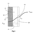
- the exterior thermal energy source provides for precise control of the reactor chamber wall inside surface temperature in a range sufficiently close to (but under) the melting point of the silicon or the reactive metal. The resulting temperature gradient is shown in FIG. 6 .
- the exterior thermal energy source may be configured into at least one temperature control zone.
- the different temperature control zones may be used to establish a different temperature profile or zone along the axial length of the reactor chamber.
- the processes disclosed herein establish a temperature gradient from the outside surface of the reactor chamber to the reaction space inside the reactor chamber as shown in FIG. 6 .
- the specific temperature gradient will vary depending upon several factors including the feedstock material, the feed rate, operating pressure within the reactor space, etc.
- the temperature gradient is time dependent since it will change beginning from start-up of the reactor to steady-state operation. Accordingly, the specific temperatures of the thermal control system will vary.
- the inside surface of the reactor chamber wall may be 1 to 300°C below the melting point of the feedstock material, more particularly 1 to 100°C below the melting point of the feedstock material;
- the skull layer may be at the melting point of the feedstock material to 300°C below the melting point of the feedstock material, more particularly the melting point to 100°C below the melting point;
- the reactor space may be at the melting point of silicon or the reactive metal up to more than 5000°C.
- the overall thermal control approach may also include thermal insulation as described below in more detail.
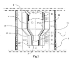
- a reactor system 1 includes at least one feedstock inlet 2, at least one liquid product outlet 3, a reactor chamber 4, an outer containment chamber 5, and a plasma generating source 6.
- the feedstock inlet 2 may be any type of port or valve that enables controlled introduction of the feedstock into the reactor chamber 4.
- the inlet 2 may be a nozzle such as a water cooled structure made from quartz, graphite and/or silicon.
- the reactor chamber 4 includes a reactor chamber wall 10 that defines a reaction space 13 located within the reactor chamber wall 10.
- the reactor chamber wall 10 includes an inside surface 11 facing the reactor space 13 and an opposing outside surface 12.
- the reactor chamber may be provided in any shape such as cylindrical, oval, rectangular, etc. Cylindrical reactor chambers are shown in the Figures. In certain embodiments, the reactor chamber may have several different sized and/or shaped sections. For example, Figure 1 depicts a first cylindrical section 14 and a second tapered or conical section 15. The second section 15 tapers into the product outlet 3.
- the reactor chamber wall 10 may be made from made from any material that resists corrosion and contamination of the feedstock or product, is amenable to skull layer formation, and offers the desired heat or energy conductive or resistant properties.
- Illustrative wall construction materials include graphite, molybdenum, tungsten, titanium, a ceramic (e.g., alumina), and quartz.
- the inside surface 11 area should be sufficiently large to enable collection and liquid conversion of the feedstock material on the inside surface 11. Depending on the desired throughput in kg/h, the inside surface 11 area should be in a range of 0.2 m 2 to 5 m 2 for a product throughput in a range of 1 to 50 kg/h.
- the power supply for generating the plasma may be any type of power supply.
- Illustrative plasmas include RF, DC arc, or microwave plasma.
- the plasma power may range from 1 to 1000 kW, more particularly 10 to 200 kW.
- the product outlet 3 may be coupled to a product collection module and/or product solidification module.
- the product can be cooled during free fall through a solidification tower and then collected in water-cooled bins if mm-sized droplets are desired.
- At least one heat induction coil(s) 20 is located at or near the outside surface 12 of the reactor chamber wall.
- the coil 20 may surround the entire periphery or only a portion of the periphery of the reactor chamber.
- the coil 20 is made from any heat transfer material that enables sufficient heating of the reactor chamber wall.
- the coil 20 also can act as a heat sink and supplement the outer water-cooled containment chamber wall that also acts as a heat sink.
- At least one resistance heater(s) 21 is disposed at or near the outside surface 12 of the reactor chamber wall.
- the resistance heater 21 heats the reactor chamber wall.
- the FIG. 2 embodiment also includes an insulation element 22 disposed between the reaction chamber wall and the containment chamber wall.
- the insulation thickness may be designed with different thicknesses along the vertical height axis of the reactor.
- the outer containment chamber 5 is shown, for example, in FIGS. 2 and 3 .
- the containment chamber 5 hermetically seals at least the reaction chamber 4.
- the containment chamber 5 includes a containment chamber wall 16 that may be water-cooled.
- the water-cooled containment chamber wall 16 also can be a heat sink for the reactor chamber thermal energies and heat flows described above.
- FIGS. 3-5 illustrate several different solidification modules that can be coupled to the reactor system.
- FIG. 3 includes an electromagnetic crucible coupled to a continuous casting system that enables the casting of silicon ingots.
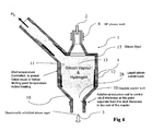
- FIG. 4 depicts a configuration that enables production of directionally solidified silicon ingot. The liquid silicon from the outlet 3 can be channeled into the electromagnetic crucible.
- the advantages of direct coupled electromagnetic casting include no additional cost for transport containers, silicon is not re-melted, and contamination is minimized since ultrapure silicon is solidified in a non-contaminating skull layer crucible.
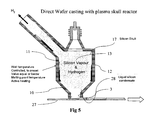
- Fig. 5 depicts a configuration that enables production direct wafer casting by introducing the liquid silicon product of the presently disclosed reactor system onto a moving horizontal support substrate 27.
- U.S. Patent No. 4,670,096 incorporated herein by reference, describes a process for direct wafer casting with liquid silicon onto a moving horizontal support.
- FIG. 3 also includes an off gas port 23 that connects to an off gas treatment system.
- Operation of the reactor system may be initiated by heating the reactor chamber wall (via thermal energy from the exterior heat source, the inner heat source, or a combination of both the exterior and the inner heat sources) to greater than the melting point of the feedstock material.
- This pre-heating with a silicon-bearing material present will form a silicon carbide layer on the graphite reactor chamber wall.
- the reactor chamber wall temperature then would be lowered so that the inside surface would be below the melting point of the feedstock material.
- the material melting in the reaction space 13 will contact the inside surface thus initiating formation of the solid (frozen) skull layer 17.
- the skull layer 17 includes an inner surface 18 and an opposing wall contact surface 19. A temperature gradient is established across the reactor chamber wall, the skull layer and the gas in the reaction space as shown in FIG. 6 .
- the skull layer thickness is no longer increasing, and the skull layer temperature reaches liquid material temperature on the surface 18 facing the reaction space 13 of the reactor.
- a liquid silicon film 28 will condense at the inner surface 18, and then flow along the inner surface 18 down the vertical axis of the reactor chamber.
- the melting process may also produce silicon vapor.
- the maximum chamber wall inside surface 11 temperature should not exceed 1414 °C (1 °C less than the melting point of silicon) during skull layer formation and steady state operation.
- the inside surface 11 temperature may range from 1115 to 1414 °C, more particularly 1215 to 1414 °C.
- the heat from the exterior thermal energy source maintains the reactor chamber wall temperatures at the desired temperature ranges allowing controlling of the skull thickness through controlling the wall temperature.
- the heat flow from the reactor chamber typically is dissipated to a heat sink external to the reactor chamber.
- the heat sink may be active cooling (e.g., water cooled-containment chamber walls) and/or passive cooling such as insulation.
- the feedstock material is introduced into the reactor chamber 4 via the inlet 2.
- the feedstock material may be any silicon-bearing material or a reactive metal.
- the silicon-bearing material may be solid silicon such as silicon powder or fines (as described in more detail herein), or a silicon-bearing gas such as silane, disilane, higher order silanes (Si n H 2n+2 ), dichlorosilane, trichlorosilane, silicon tetrachloride, dibromosilane, tribromosilane, silicon tetrabromide, diiodosilane, triiodosilane, silicon tetraiodide or a mixture thereof.
- the silicon powder introduced into the reactor system may be small silicon particles (fines/powder) produced from silicon handling (e.g., breaking, grinding or cutting) or by any process that decomposes a silicon-containing gas.
- the powder may be dispersed or suspended in a carrier medium for injecting into the reactor system.
- the carrier medium may be a gas that is inert to silicon and/or that has a relatively low ionization potential such as Ar.
- the operating pressure in the reaction space 13 may range from 0.1 bar to 2.0 bar, more particularly 0.5 bar to 2.0 bar.
- the critical temperature is the thermal decomposition temperature at which the gas decomposes into a liquid.
- the inside surface of the reactor chamber wall is maintained at an equilibrium temperature below the melting point temperature.
- the embodiments shown in FIGS. 4 and 5 enable the production of a silicon ingot ( FIG. 4 ) or a wafer ( FIG. 5 ) directly from a silicon-bearing gas (e.g., silane) feedstock thus avoiding the costly step of forming, re-melting and cutting of polycrystalline silicon.
- a second gas, hydrogen is present with the silicon-bearing gas in the reaction space 13. The hydrogen results from the thermal decomposition of the SiH 4 to Si and hydrogen.
- the skull layer should have a thickness that is sufficient to protect against contamination of the liquid product by the reactor chamber wall material.
- the skull layer thickness should not so great that it occupies an unnecessary amount of the space inside the reactor chamber, thus detrimentally diminishing the available reaction space.
- An unnecessarily thick skull layer will also be more difficult to be thermally controlled at the equilibrium thickness.
- the average skull layer thickness should be 0.01 to 200 mm, more particularly 0.1 to 30 mm.
- Liquid silicon or liquid reactive metal flows through the liquid product outlet 3.
- the geometrical form (and size) of the liquid product can be controlled by the design of the product outlet 3.
- the outlet 3 can be designed to discharge (e.g., jetting through a nozzle) droplets or spheres (which are the preferred physical form of feedstock for mono- or multi-crystalline ingot production).
- these droplets can be solidified in free fall through a solidification tower.
- the droplets can be collected in a container at the bottom of the solidification tower or can be pneumatically conveyed into a collection container.
- the outlet 3 also can be vibrated or subjected to a gas stream to influence the size of the droplets.
Landscapes
- Chemical & Material Sciences (AREA)
- Organic Chemistry (AREA)
- Plasma & Fusion (AREA)
- Physics & Mathematics (AREA)
- Engineering & Computer Science (AREA)
- Spectroscopy & Molecular Physics (AREA)
- Inorganic Chemistry (AREA)
- Health & Medical Sciences (AREA)
- General Health & Medical Sciences (AREA)
- Toxicology (AREA)
- Chemical Kinetics & Catalysis (AREA)
- Silicon Compounds (AREA)
- Physical Or Chemical Processes And Apparatus (AREA)
Description
- The disclosure relates to methods, apparatus and systems for treating a silicon-bearing material or a reactive metal material.
- Ultrapure or high-grade polycrystalline silicon (polysilicon) is a critical raw material for both the semiconductor (SC) and photovoltaic (PV) industries. While there are alternatives for specific PV applications, polysilicon will remain the preferred raw material in the near and foreseeable future. Hence, improving the availability of and economics for producing polysilicon will increase the growth opportunities for both industries.
- The majority of polysilicon is produced by the commonly called Siemens hot-wire method with silane or trichlorosilane (TCS) as the silicon-bearing gas (SBG) source. The SBG, usually mixed in other inert or reaction gases, is pyrolytically decomposed and deposited onto a heated silicon filament. Another method is the pyrolytic decomposition of SBG in fluidized beds. This is an attractive alternative to produce polysilicon for the PV and semiconductor industries due to significantly lower energy consumption and the possibility for continuous production. These benefits stem from the excellent mass and heat transfer and increased surface for deposition. Compared with the Siemens-type reactor, the fluidized bed reactor offers considerably higher production rates at a fraction of the energy consumption. The fluidized bed reactor will also be more continuous and highly automated to significantly reduce labor costs as well.
- Silane, or higher order silanes, used as the SBG in the Siemens or fluidized bed reactor process has a disadvantage over TCS in that it can undergo a (homogeneous) gas phase decomposition to powder particles in addition to the (heterogeneous) polysilicon deposition. The temperature at which the decomposition occurs is called the critical nucleation temperature (CNT). The CNT depends on the SBG species, SBG partial pressure, total pressure and type of inert dilution gas. Once the CNT is reached, the particle concentration will increase 104-106 times over a 1-5 °C range. Nucleus silicon powder particles are typically 1-100 nm in size depending on the residence time and can be amorphous or crystalline. In either case, there exists a moderate concentration of non-bonded electrons on the surface of these particles, which enables the particles to readily agglomerate into larger powder particles. Depending on conditions, this powder can be anything from non-single nuclei particles, micron-sized round agglomerates to large particles extended to several 100 microns.
- These powder particles (also known as silicon fines) are considered contaminants in the Siemens process if the polysilicon is subsequently used for the growth of a dislocation-free single crystal, particularly in the semiconductor industry. Therefore, in a Siemens process with silane or higher order silanes as the SBG, the reactor walls are kept cool, applying thermophoresis to drive the powder particles from the region near the hot rods where they are produced towards the cool reactor walls where they deposit. Removing the powder from the gas phase reduces the potential for contamination of the silicon rod.
- In a fluidized bed reactor process, powder may adhere to granules and incorporate in the particle, thus contributing to the overall granular growth. However, a large portion of the powder will be entrained out of the fluid bed reactor with the outgoing gases. In a fluidized bed reactor process for granular silicon production, such fine silicon powder is considered a production loss since it does not contribute to granular material.
- Silicon powder may also be produced in other SBG deposition processes, e.g., intentionally in a Free Space Reactor or unintentionally in Chemical Vapor Deposition (CVD) reactor for thin film deposition on a substrate. Another source of silicon powder is silicon ingot grinding or cutting. The production rates and silicon qualities vary considerably depending on the processes.
- Powder produced as described in the processes above currently is recovered with great difficulty because it is a fluffy, low density, high surface area product, easily contaminated by airborne substances. In addition, the silicon powder is typically disposed of as a waste product or is offered at very low value into the merchant silicon market.
-
US4188368 discloses a method of producing silicon using arc heaters to heat a carrier gas injected via a plurality of ports.US4787986 discloses a process for melting silicon powder using a melting crucible.US4343772 discloses a thermal reactor apparatus for pyrolytically decomposing silane gas into liquid silicon. - The invention is defined in the appended claims.
- Disclosed herein are methods for thermally treating a silicon-bearing material or a reactive metal in order to convert this material into a more useful product form. For example, the disclosed methods upgrade silicon powder from a low-grade, loose-packed, high surface area product to a silicon feedstock suitable for PV and SC processing requirements. Avoiding contamination during the thermal treatment process is important for obtaining pure, particularly ultrapure, product. One contamination source is the materials that constitute the structural elements of the reactor system. According to the apparatus, systems and methods disclosed herein a skull layer comprising solid silicon or solid reactive metal is formed on at least a portion of the inside surface of the reactor. The solid skull layer prevents contact of the feed material and product with the surface of the reactor system, thus avoiding or minimizing contamination. The skull layer also may provide a diffusion barrier for preventing migration of reactor wall elements into the silicon product.
- According to one embodiment, a method for producing silicon or a reactive metal is disclosed herein that comprises:
- introducing a silicon-bearing feed or reactive metal feed into a reactor chamber, wherein the reactor chamber includes a reactor chamber wall having (i) an inside surface facing a reaction space and (ii) an opposing outside surface;
- generating a first thermal energy within the reaction space sufficient to generate a liquid silicon product or a liquid reactive metal product;
- generating a second thermal energy exterior to the reactor chamber wall such that a heat flow from the second thermal energy initially impacts the outside surface of the reactor chamber wall; and
- establishing an inside surface wall temperature within a temperature range that is above or below a melting point temperature of the silicon or the reactive metal by controlling the first thermal energy source and the second thermal energy source.
- In a further embodiment, a method for producing silicon is disclosed that comprises:
- introducing silicon powder into a reactor chamber, wherein the reactor chamber includes a reactor chamber wall having (i) an inside surface facing a reaction space and (ii) an opposing outside surface;
- generating a plasma in the reactor space;
- thermally melting the silicon powder by subjecting the silicon powder to a temperature greater than the melting point of the silicon powder via the plasma, wherein the melting process produces liquid silicon;
- maintaining the inside surface of the reactor chamber wall at an equilibrium temperature below the melting point of the silicon powder while thermally melting the silicon powder; and
- solidifying the liquid silicon after it exits the reactor chamber.
- An additional disclosed embodiment concerns a method for producing solid multicrystalline silicon that comprises:
- introducing a silicon-bearing gas into a reactor chamber, wherein the reaction chamber includes a reactor chamber wall having (i) an inside surface facing a reaction space and (ii) an opposing outside surface, and a product outlet;
- generating a plasma in the reactor space;
- thermally decomposing the silicon-bearing gas by subjecting the silicon-bearing gas to a sufficient temperature to produce liquid silicon;
- maintaining the inside surface of the reactor chamber wall at an equilibrium temperature below the melting point temperature of silicon while thermally decomposing the silicon-bearing gas; and
- introducing the liquid silicon from the product outlet directly into a module for casting the liquid silicon into solid multicrystalline silicon ingot or wafer.
- An additional method for producing silicon disclosed herein includes:
- introducing silane gas into a reactor chamber, wherein the reaction chamber includes a reactor chamber wall having (i) an inside surface facing a reaction space and (ii) an opposing outside surface, and a product outlet;
- generating a plasma in the reactor space;
- thermally decomposing the silane gas by subjecting the silane gas to the plasma to produce liquid silicon; and
- maintaining the inside surface of the reactor chamber wall at an equilibrium temperature below the melting point temperature of silicon while thermally decomposing the silane gas.
- Also disclosed herein is a reactor system that comprises:
- a silicon-bearing feedstock or a reactive metal feedstock;
- a reaction chamber that includes a reactor chamber wall that defines a chamber reaction space and includes (i) an inside surface facing the reaction space and (ii) an opposing outside surface;
- a plasma energy source coupled to the reaction chamber and configured to generate thermal energy within the chamber reaction space;
- an exterior thermal energy source configured to subject the outside surface of the reactor chamber wall to heating, and located outside of the reactor chamber; and
- a product outlet configured for withdrawing liquid silicon or liquid reactive metal from the reaction chamber.
- In a preferred form, an adjustable energy flow of 1 to 2000kW/m2 from the reaction space through the reactor chamber wall is produced by controlling the first thermal energy source and the second energy source.
- The foregoing will become more apparent from the following detailed description, which proceeds with reference to the accompanying figures.
-
-
FIGS. 1A and 1B are schematics of one embodiment of the disclosed reactor system.FIG. 1A is an exploded view of a wall section of the reactor shown inFIG. 1B . -
FIG. 2 is a schematic of a further embodiment of the disclosed reactor system. -
FIG. 3 is a schematic of a reactor system that includes one solidification embodiment. -
FIG. 4 is a schematic of a reactor system that includes another solidification embodiment. -
FIG. 5 is a schematic of a reactor system that includes a further solidification embodiment. -
FIG. 6 is a schematic of a temperature gradient in the disclosed reactor system. -
FIG. 7 is a schematic of two heat flows in the disclosed reactor system. - In the figures like reference numerals refer to like elements unless otherwise specified.
- The singular terms "a," "an," and "the" include plural referents unless context clearly indicates otherwise. The word "comprises" indicates "includes." Unless otherwise indicated, description of components in chemical nomenclature refers to the components at the time of addition to any combination specified in the description, but does not necessarily preclude chemical interactions among the components of a mixture once mixed. Any numerical values recited herein include all values from the lower value to the upper value in increments of one unit provided that there is a separation of at least 2 units between any lower value and any higher value. As an example, if it is stated that the amount of a component or a value of a process variable is from 1 to 90, preferably from 20 to 80, more preferably from 30 to 70, it is intended that values such as 15 to 85, 22 to 68, 43 to 51, 30 to 32 etc., are expressly enumerated in this specification. For values, which have less than one unit difference, one unit is considered to be 0.1, 0.01, 0.001, or 0.0001 as appropriate. Thus all possible combinations of numerical values between the lowest value and the highest value enumerated herein are said to be expressly stated in this application.
- The reactor systems disclosed herein are thermally designed to maintain a substantially solid skull layer of silicon or the reactive metal feed on an inside surface of a reactor chamber wall. Moreover, the thermal design of the system enables more precise controlling of the skull layer thickness. The skull layer may cover only a portion of the inside wall surface or it may cover the entire surface area of the inside surface. Formation of the solid skull layer on the inside surface of the reactor chamber wall protects the chamber wall construction material from corrosive attack by the liquid silicon or the liquid reactive metal. In other words, the skull layer prevents direct contact between the chamber wall and the liquid silicon thus minimizing contamination of the liquid silicon product. The skull layer is formed by maintaining the inside surface of the reactor chamber wall at a temperature below the melting point of the silicon or the respective reactive metal melting point.
- The thermal control system includes a combination of an inner thermal energy source inside the reactor chamber and an exterior thermal energy source located outside or external to the reactor chamber. The exterior thermal energy source is also located within a confinement chamber that also encompasses the reactor chamber. The exterior thermal energy source may provide heat directly to the outside surface of the reactor wall via induction heating, resistance heating, or a combination of both. In an embodiment shown in
FIGS. 1A, 1B ,3 , and7B the exterior energy source is an induction coil(s). In another embodiment shown inFIG. 2 , the exterior energy source is a resistance heater(s). Microwave is another possible exterior energy source. The inner thermal energy source may be a plasma as described in more detail below. Alternatively, the inner thermal energy source may be electron beams, resistance heating elements or induction heating elements. - The heat flows generated by the inner thermal energy source and the exterior energy source are shown in
FIG. 7A and 7B , respectively. The inner heat flow progresses as follows: a heated reaction gas → liquid silicon film → solid silicon skull layer → reactor chamber wall. The exterior heat flow progresses as follows: reactor chamber wall → solid silicon skull layer → liquid silicon film. The inner thermal energy source provides the energy for the thermal decomposition of the feedstock material. The exterior thermal energy source provides for precise control of the reactor chamber wall inside surface temperature in a range sufficiently close to (but under) the melting point of the silicon or the reactive metal. The resulting temperature gradient is shown inFIG. 6 . - The exterior thermal energy source may be configured into at least one temperature control zone. The different temperature control zones may be used to establish a different temperature profile or zone along the axial length of the reactor chamber.
- As described above, the processes disclosed herein establish a temperature gradient from the outside surface of the reactor chamber to the reaction space inside the reactor chamber as shown in
FIG. 6 . The specific temperature gradient will vary depending upon several factors including the feedstock material, the feed rate, operating pressure within the reactor space, etc. In addition, the temperature gradient is time dependent since it will change beginning from start-up of the reactor to steady-state operation. Accordingly, the specific temperatures of the thermal control system will vary. However, in general, the inside surface of the reactor chamber wall may be 1 to 300°C below the melting point of the feedstock material, more particularly 1 to 100°C below the melting point of the feedstock material; the skull layer may be at the melting point of the feedstock material to 300°C below the melting point of the feedstock material, more particularly the melting point to 100°C below the melting point; and the reactor space may be at the melting point of silicon or the reactive metal up to more than 5000°C. - The overall thermal control approach may also include thermal insulation as described below in more detail.
- Illustrative embodiments of the reactor system are shown in
FIGS. 1-5 . In general, areactor system 1 includes at least onefeedstock inlet 2, at least oneliquid product outlet 3, areactor chamber 4, anouter containment chamber 5, and aplasma generating source 6. - The
feedstock inlet 2 may be any type of port or valve that enables controlled introduction of the feedstock into thereactor chamber 4. For example, theinlet 2 may be a nozzle such as a water cooled structure made from quartz, graphite and/or silicon. - The
reactor chamber 4 includes areactor chamber wall 10 that defines areaction space 13 located within thereactor chamber wall 10. Thereactor chamber wall 10 includes aninside surface 11 facing thereactor space 13 and an opposingoutside surface 12. The reactor chamber may be provided in any shape such as cylindrical, oval, rectangular, etc. Cylindrical reactor chambers are shown in the Figures. In certain embodiments, the reactor chamber may have several different sized and/or shaped sections. For example,Figure 1 depicts a firstcylindrical section 14 and a second tapered orconical section 15. Thesecond section 15 tapers into theproduct outlet 3. Thereactor chamber wall 10 may be made from made from any material that resists corrosion and contamination of the feedstock or product, is amenable to skull layer formation, and offers the desired heat or energy conductive or resistant properties. Illustrative wall construction materials include graphite, molybdenum, tungsten, titanium, a ceramic (e.g., alumina), and quartz. - The
inside surface 11 area should be sufficiently large to enable collection and liquid conversion of the feedstock material on theinside surface 11. Depending on the desired throughput in kg/h, theinside surface 11 area should be in a range of 0.2 m2 to 5 m2 for a product throughput in a range of 1 to 50 kg/h. - The power supply for generating the plasma may be any type of power supply. Illustrative plasmas include RF, DC arc, or microwave plasma. Depending upon the specific plasma type, the plasma power may range from 1 to 1000 kW, more particularly 10 to 200 kW.
- The
product outlet 3 may be coupled to a product collection module and/or product solidification module. For example, the product can be cooled during free fall through a solidification tower and then collected in water-cooled bins if mm-sized droplets are desired. - In the embodiment of
FIGS. 1A and 1B , at least one heat induction coil(s) 20 is located at or near theoutside surface 12 of the reactor chamber wall. Thecoil 20 may surround the entire periphery or only a portion of the periphery of the reactor chamber. Thecoil 20 is made from any heat transfer material that enables sufficient heating of the reactor chamber wall. Thecoil 20 also can act as a heat sink and supplement the outer water-cooled containment chamber wall that also acts as a heat sink. - In the embodiment of
FIG. 2 , at least one resistance heater(s) 21 is disposed at or near theoutside surface 12 of the reactor chamber wall. Theresistance heater 21 heats the reactor chamber wall. TheFIG. 2 embodiment also includes aninsulation element 22 disposed between the reaction chamber wall and the containment chamber wall. The insulation thickness may be designed with different thicknesses along the vertical height axis of the reactor. - The
outer containment chamber 5 is shown, for example, inFIGS. 2 and3 . Thecontainment chamber 5 hermetically seals at least thereaction chamber 4. Thecontainment chamber 5 includes acontainment chamber wall 16 that may be water-cooled. The water-cooledcontainment chamber wall 16 also can be a heat sink for the reactor chamber thermal energies and heat flows described above. -
FIGS. 3-5 illustrate several different solidification modules that can be coupled to the reactor system. -
FIG. 3 includes an electromagnetic crucible coupled to a continuous casting system that enables the casting of silicon ingots.FIG. 4 depicts a configuration that enables production of directionally solidified silicon ingot. The liquid silicon from theoutlet 3 can be channeled into the electromagnetic crucible. The advantages of direct coupled electromagnetic casting include no additional cost for transport containers, silicon is not re-melted, and contamination is minimized since ultrapure silicon is solidified in a non-contaminating skull layer crucible.Fig. 5 depicts a configuration that enables production direct wafer casting by introducing the liquid silicon product of the presently disclosed reactor system onto a movinghorizontal support substrate 27.U.S. Patent No. 4,670,096 , incorporated herein by reference, describes a process for direct wafer casting with liquid silicon onto a moving horizontal support. -
FIG. 3 also includes an offgas port 23 that connects to an off gas treatment system. - Operation of the reactor system may be initiated by heating the reactor chamber wall (via thermal energy from the exterior heat source, the inner heat source, or a combination of both the exterior and the inner heat sources) to greater than the melting point of the feedstock material. This pre-heating with a silicon-bearing material present will form a silicon carbide layer on the graphite reactor chamber wall. The reactor chamber wall temperature then would be lowered so that the inside surface would be below the melting point of the feedstock material. The material melting in the
reaction space 13 will contact the inside surface thus initiating formation of the solid (frozen)skull layer 17. Theskull layer 17 includes aninner surface 18 and an opposingwall contact surface 19. A temperature gradient is established across the reactor chamber wall, the skull layer and the gas in the reaction space as shown inFIG. 6 . At thermal equilibrium conditions the skull layer thickness is no longer increasing, and the skull layer temperature reaches liquid material temperature on thesurface 18 facing thereaction space 13 of the reactor. Aliquid silicon film 28 will condense at theinner surface 18, and then flow along theinner surface 18 down the vertical axis of the reactor chamber. The melting process may also produce silicon vapor. - In the case of a silicon-bearing material feedstock, the maximum chamber wall inside
surface 11 temperature should not exceed 1414 °C (1 °C less than the melting point of silicon) during skull layer formation and steady state operation. In certain embodiments theinside surface 11 temperature may range from 1115 to 1414 °C, more particularly 1215 to 1414 °C. The heat from the exterior thermal energy source maintains the reactor chamber wall temperatures at the desired temperature ranges allowing controlling of the skull thickness through controlling the wall temperature. - The heat flow from the reactor chamber typically is dissipated to a heat sink external to the reactor chamber. The heat sink may be active cooling (e.g., water cooled-containment chamber walls) and/or passive cooling such as insulation.
- The feedstock material is introduced into the
reactor chamber 4 via theinlet 2. The feedstock material may be any silicon-bearing material or a reactive metal. The silicon-bearing material may be solid silicon such as silicon powder or fines (as described in more detail herein), or a silicon-bearing gas such as silane, disilane, higher order silanes (SinH2n+2), dichlorosilane, trichlorosilane, silicon tetrachloride, dibromosilane, tribromosilane, silicon tetrabromide, diiodosilane, triiodosilane, silicon tetraiodide or a mixture thereof. Reactive metals such as titanium or zirconium could also be reduced using the process and apparatus disclosed herein. The silicon powder introduced into the reactor system may be small silicon particles (fines/powder) produced from silicon handling (e.g., breaking, grinding or cutting) or by any process that decomposes a silicon-containing gas. The powder may be dispersed or suspended in a carrier medium for injecting into the reactor system. For example, the carrier medium may be a gas that is inert to silicon and/or that has a relatively low ionization potential such as Ar. - The operating pressure in the
reaction space 13 may range from 0.1 bar to 2.0 bar, more particularly 0.5 bar to 2.0 bar. - If the feedstock material is a silicon-bearing gas, the critical temperature is the thermal decomposition temperature at which the gas decomposes into a liquid. Thus, the inside surface of the reactor chamber wall is maintained at an equilibrium temperature below the melting point temperature. The embodiments shown in
FIGS. 4 and5 enable the production of a silicon ingot (FIG. 4 ) or a wafer (FIG. 5 ) directly from a silicon-bearing gas (e.g., silane) feedstock thus avoiding the costly step of forming, re-melting and cutting of polycrystalline silicon. A second gas, hydrogen, is present with the silicon-bearing gas in thereaction space 13. The hydrogen results from the thermal decomposition of the SiH4 to Si and hydrogen. - The skull layer should have a thickness that is sufficient to protect against contamination of the liquid product by the reactor chamber wall material. However, the skull layer thickness should not so great that it occupies an unnecessary amount of the space inside the reactor chamber, thus detrimentally diminishing the available reaction space. An unnecessarily thick skull layer will also be more difficult to be thermally controlled at the equilibrium thickness. In general, the average skull layer thickness should be 0.01 to 200 mm, more particularly 0.1 to 30 mm.
- Liquid silicon or liquid reactive metal flows through the
liquid product outlet 3. The geometrical form (and size) of the liquid product can be controlled by the design of theproduct outlet 3. For example, theoutlet 3 can be designed to discharge (e.g., jetting through a nozzle) droplets or spheres (which are the preferred physical form of feedstock for mono- or multi-crystalline ingot production). In one embodiment, these droplets can be solidified in free fall through a solidification tower. The droplets can be collected in a container at the bottom of the solidification tower or can be pneumatically conveyed into a collection container. Theoutlet 3 also can be vibrated or subjected to a gas stream to influence the size of the droplets. - In view of the many possible embodiments to which the principles of the disclosed process, apparatus and system may be applied, it should be recognized that the illustrated embodiments are only preferred examples and should not be taken as limiting the scope of the invention.
Claims (14)
- A method for producing silicon or a reactive metal, comprising:introducing a silicon-bearing feed or reactive metal-bearing feed into a reactor chamber, wherein the reactor chamber includes a reactor chamber wall having (i) an inside surface facing a reaction space and (ii) an opposing outside surface;generating a first thermal energy within the reaction space sufficient to generate a liquid silicon product or a liquid reactive metal product;generating a second thermal energy exterior to the reactor chamber wall such that a heat flow from the second thermal energy initially impacts the outside surface of the reactor chamber wall; andestablishing an inside surface wall temperature within a temperature range that is below a melting point temperature of the silicon or the reactive metal by controlling the first thermal energy source and the second thermal energy source.
- The method of claim 1, wherein an adjustable energy flow of 1 to 2000 kW/m2 from the reaction space through the reactor chamber wall is produced by controlling the first thermal energy source and the second thermal energy source.
- The method of claim 1, wherein the first thermal energy is plasma energy and the second thermal energy is induction heating or resistance heating.
- The method of claim 1, further comprising forming a solid skull layer of silicon or the reactive metal on the inside surface of the reactor chamber wall, preferably wherein the solid skull layer has a thickness of less than 200 mm.
- The method of claim 1, wherein the first thermal energy generates heat within the reactor space at a temperature above the melting point of silicon, and the first energy source and the second energy source combine to maintain the inside surface wall temperature at a temperature below the melting point of silicon.
- The method of claim 1, wherein the reactor chamber wall is vertically aligned such that the liquid silicon or liquid metal can flow down the chamber wall.
- The method of claim 1, wherein heat from the second thermal energy is controlled to maintain the inside surface wall temperature at a temperature below the melting point temperature of the silicon-bearing feed or the reactive metal feed, preferably wherein the inside surface wall temperature is maintained at 1 to 300°C below the melting point temperature of silicon or the reactive metal.
- The method of claim 1, wherein a silicon-bearing feed is introduced into the reaction chamber and the second thermal energy maintains the inside surface wall temperature at a temperature of 1115 to 1414°C.
- The method of claim 1 further comprising:introducing silicon powder into said reactor chamber wherein generating a first thermal energy comprises generating a plasma in the reactor space;the method further comprising:thermally melting the silicon powder by subjecting the silicon powder to a temperature greater than the melting point of the silicon powder via the plasma, wherein the melting process produces liquid silicon;maintaining the inside surface of the reactor chamber wall at an equilibrium temperature below the melting point of the silicon powder while melting the silicon powder; andsolidifying the liquid silicon after it exits the reactor chamber.
- The method of claim 9, further comprising controllably heating the outside surface of the reactor chamber wall.
- The method of claim 1 wherein generating said first thermal energy within the reaction space is sufficient to generate a heated reaction gas and a liquid silicon product or a liquid reactive metal product;
the method further comprising:forming a solid skull layer of silicon or the reactive metal on the inside surface of the reactor chamber wall; andforming a film of the liquid silicon product or the liquid reactive metal product such that the film flows down on at least a portion of the solid skull layer;wherein the first thermal energy generates a first heat flow that progress as follows: heated reaction gas → liquid silicon or reactive metal film → solid silicon or reactive metal skull layer → reactor chamber wall, and the second thermal energy generates a second heat flow that progresses as follows: reactor chamber wall → solid silicon or reactive metal skull layer → liquid silicon or reactive metal film. - The method of claim 1, wherein the silicon-bearing feed is a silicon- bearing gas selected from SinH2n+2, wherein n is 1 to 4, dichlorosilane, trichlorosilane, silicon tetrachloride, dibromosilane, tribromosilane, silicon tetrabromide, diiodosilane, triiodosilane, silicon tetraiodide or a mixture thereof.
- A reactor system, comprising:a silicon-bearing feedstock or a reactive metal feedstock;a reaction chamber that includes a reactor chamber wall that defines a chamber reaction space and includes (i) an inside surface facing the reaction space and (ii) an opposing outside surface;a plasma energy source coupled to the reaction chamber and configured to generate thermal energy within the chamber reaction space;an exterior thermal energy source configured to subject the outside surface of the reactor chamber wall to heating, and located outside of the reactor chamber; anda product outlet configured for withdrawing liquid silicon or liquid reactive metal from the reaction chamber.
- The reactor system of claim 13, further comprising:means for injecting a silicon powder feedstock into the reaction chamber; ora hermetically sealed containment chamber encompassing at least the reactor chamber and the exterior thermal energy source; ormeans for vibrating the product outlet;and preferably wherein the exterior energy source comprises at least one induction coil disposed around a portion of the outside surface of the reactor chamber wall or wherein the exterior energy source comprises at least one resistance heater disposed in contact with a portion of the outside surface of the reactor chamber wall.
Applications Claiming Priority (3)
| Application Number | Priority Date | Filing Date | Title |
|---|---|---|---|
| US12884708P | 2008-05-23 | 2008-05-23 | |
| US12/378,250 US20100047148A1 (en) | 2008-05-23 | 2009-02-11 | Skull reactor |
| PCT/US2009/044712 WO2009143271A2 (en) | 2008-05-23 | 2009-05-20 | Skull reactor |
Publications (3)
| Publication Number | Publication Date |
|---|---|
| EP2294005A2 EP2294005A2 (en) | 2011-03-16 |
| EP2294005A4 EP2294005A4 (en) | 2012-01-04 |
| EP2294005B1 true EP2294005B1 (en) | 2013-03-27 |
Family
ID=41340864
Family Applications (1)
| Application Number | Title | Priority Date | Filing Date |
|---|---|---|---|
| EP09751499A Not-in-force EP2294005B1 (en) | 2008-05-23 | 2009-05-20 | Method and skull reactor for producing silicon or a reactive metal |
Country Status (9)
| Country | Link |
|---|---|
| US (1) | US20100047148A1 (en) |
| EP (1) | EP2294005B1 (en) |
| JP (1) | JP2011520760A (en) |
| KR (1) | KR20110034608A (en) |
| CN (1) | CN102083751A (en) |
| CA (1) | CA2725062A1 (en) |
| ES (1) | ES2408630T3 (en) |
| TW (1) | TW201009136A (en) |
| WO (1) | WO2009143271A2 (en) |
Families Citing this family (7)
| Publication number | Priority date | Publication date | Assignee | Title |
|---|---|---|---|---|
| US20100189926A1 (en) * | 2006-04-14 | 2010-07-29 | Deluca Charles | Plasma deposition apparatus and method for making high purity silicon |
| FR2944520B1 (en) * | 2009-04-17 | 2011-05-20 | Similelt | PROCESS AND INSTALLATION FOR THE PURIFICATION OF METALLURGICAL SILICON. |
| DE102010015354A1 (en) * | 2010-04-13 | 2011-10-13 | Schmid Silicon Technology Gmbh | Production of a crystalline semiconductor material |
| JP6850004B2 (en) * | 2015-04-29 | 2021-03-31 | 1366 テクノロジーズ インク. | How to maintain the volume of molten material in which the material is consumed and replenished |
| CN107973300B (en) * | 2016-10-25 | 2024-01-05 | 江苏中能硅业科技发展有限公司 | Liquid silicon production device and method |
| DE102017125723A1 (en) * | 2017-04-25 | 2018-10-25 | Eeplasma Gmbh | Method and apparatus for growing a single crystal |
| DE102019209898A1 (en) * | 2019-07-04 | 2021-01-07 | Schmid Silicon Technology Gmbh | Apparatus and method for forming liquid silicon |
Family Cites Families (28)
| Publication number | Priority date | Publication date | Assignee | Title |
|---|---|---|---|---|
| US4049384A (en) * | 1975-04-14 | 1977-09-20 | Arthur D. Little, Inc. | Cold crucible system |
| US4188368A (en) * | 1978-03-29 | 1980-02-12 | Nasa | Method of producing silicon |
| US4212343A (en) * | 1979-03-16 | 1980-07-15 | Allied Chemical Corporation | Continuous casting method and apparatus for structurally defined metallic strips |
| US4274473A (en) * | 1980-01-14 | 1981-06-23 | Allied Chemical Corporation | Contour control for planar flow casting of metal ribbon |
| US4343772A (en) * | 1980-02-29 | 1982-08-10 | Nasa | Thermal reactor |
| CA1147698A (en) * | 1980-10-15 | 1983-06-07 | Maher I. Boulos | Purification of metallurgical grade silicon |
| DE3419137A1 (en) * | 1984-05-23 | 1985-11-28 | Bayer Ag, 5090 Leverkusen | METHOD AND DEVICE FOR PRODUCING SEMICONDUCTOR FILMS |
| DE3629231A1 (en) * | 1986-08-28 | 1988-03-03 | Heliotronic Gmbh | METHOD FOR MELTING SILICON POWDER CHARGED IN A MELTING POT, AND MELTING POT FOR CARRYING OUT THE METHOD |
| US4936375A (en) * | 1988-10-13 | 1990-06-26 | Axel Johnson Metals, Inc. | Continuous casting of ingots |
| US5842511A (en) * | 1996-08-19 | 1998-12-01 | Alliedsignal Inc. | Casting wheel having equiaxed fine grain quench surface |
| BR9611816A (en) * | 1996-10-14 | 1999-07-13 | Kawasaki Steel Co | Process and apparatus for making polycrystalline silicon and process for making silicon wafers for solar batteries |
| FR2772741B1 (en) * | 1997-12-19 | 2000-03-10 | Centre Nat Rech Scient | PROCESS AND INSTALLATION FOR REFINING SILICON |
| US6468886B2 (en) * | 1999-06-15 | 2002-10-22 | Midwest Research Institute | Purification and deposition of silicon by an iodide disproportionation reaction |
| JP3646570B2 (en) * | 1999-07-01 | 2005-05-11 | 三菱住友シリコン株式会社 | Silicon continuous casting method |
| EP1254861B1 (en) * | 2000-12-28 | 2008-01-30 | Sumco Corporation | Silicon continuous casting method |
| US6960537B2 (en) * | 2001-10-02 | 2005-11-01 | Asm America, Inc. | Incorporation of nitrogen into high k dielectric film |
| US7082986B2 (en) * | 2002-02-08 | 2006-08-01 | Cornell Research Foundation, Inc. | System and method for continuous casting of a molten material |
| US7175685B1 (en) * | 2002-04-15 | 2007-02-13 | Gt Solar Incorporated | Dry conversion of high purity ultrafine silicon powder to densified pellet form for silicon melting applications |
| RU2213792C1 (en) * | 2002-04-19 | 2003-10-10 | Бурлов Юрий Александрович | Plasma-type reactor-separator |
| US6780219B2 (en) * | 2002-07-03 | 2004-08-24 | Osram Sylvania Inc. | Method of spheridizing silicon metal powders |
| JP2005033173A (en) * | 2003-06-16 | 2005-02-03 | Renesas Technology Corp | Method for manufacturing semiconductor integrated circuit device |
| JP4235066B2 (en) * | 2003-09-03 | 2009-03-04 | 日本エー・エス・エム株式会社 | Thin film formation method |
| US20070207268A1 (en) * | 2003-12-08 | 2007-09-06 | Webb R K | Ribbed CVC structures and methods of producing |
| US7141114B2 (en) * | 2004-06-30 | 2006-11-28 | Rec Silicon Inc | Process for producing a crystalline silicon ingot |
| US7396415B2 (en) * | 2005-06-02 | 2008-07-08 | Asm America, Inc. | Apparatus and methods for isolating chemical vapor reactions at a substrate surface |
| JP2008050256A (en) * | 2006-07-28 | 2008-03-06 | Kyocera Corp | Method of manufacturing granular crystal, and apparatus of manufacturing granular crystal |
| JP5141020B2 (en) * | 2007-01-16 | 2013-02-13 | 株式会社Sumco | Casting method of polycrystalline silicon |
| US20090289390A1 (en) * | 2008-05-23 | 2009-11-26 | Rec Silicon, Inc. | Direct silicon or reactive metal casting |
-
2009
- 2009-02-11 US US12/378,250 patent/US20100047148A1/en not_active Abandoned
- 2009-05-12 TW TW098115642A patent/TW201009136A/en unknown
- 2009-05-20 CA CA2725062A patent/CA2725062A1/en not_active Abandoned
- 2009-05-20 JP JP2011510687A patent/JP2011520760A/en active Pending
- 2009-05-20 KR KR1020107028967A patent/KR20110034608A/en not_active Application Discontinuation
- 2009-05-20 ES ES09751499T patent/ES2408630T3/en active Active
- 2009-05-20 WO PCT/US2009/044712 patent/WO2009143271A2/en active Application Filing
- 2009-05-20 EP EP09751499A patent/EP2294005B1/en not_active Not-in-force
- 2009-05-20 CN CN200980118728.1A patent/CN102083751A/en active Pending
Also Published As
| Publication number | Publication date |
|---|---|
| WO2009143271A3 (en) | 2010-02-25 |
| TW201009136A (en) | 2010-03-01 |
| CN102083751A (en) | 2011-06-01 |
| US20100047148A1 (en) | 2010-02-25 |
| KR20110034608A (en) | 2011-04-05 |
| ES2408630T3 (en) | 2013-06-21 |
| EP2294005A4 (en) | 2012-01-04 |
| CA2725062A1 (en) | 2009-11-26 |
| EP2294005A2 (en) | 2011-03-16 |
| WO2009143271A2 (en) | 2009-11-26 |
| JP2011520760A (en) | 2011-07-21 |
Similar Documents
| Publication | Publication Date | Title |
|---|---|---|
| US20090289390A1 (en) | Direct silicon or reactive metal casting | |
| KR101026815B1 (en) | Process for the continuous production of polycrystalline high-purity silicon granules | |
| EP2294005B1 (en) | Method and skull reactor for producing silicon or a reactive metal | |
| KR100411180B1 (en) | Method for preparing polycrystalline silicon | |
| JP3122643B2 (en) | Method for producing high-purity silicon particles | |
| JP5886831B2 (en) | Generation of single crystal semiconductor materials | |
| JP4157281B2 (en) | Reactor for silicon production | |
| JP4639004B2 (en) | Silicon manufacturing apparatus and manufacturing method | |
| US10196273B2 (en) | Device for manufacturing polysilicon using horizontal reactor and method for manufacturing same | |
| TWI551735B (en) | Production of a crystalline semiconductor material | |
| KR20170108881A (en) | Ultra-high temperature precipitation process for preparing polycrystalline silicon | |
| JPH06127926A (en) | Production of granular polycrystalline silicon | |
| JPH06127921A (en) | Production of granular polycrystalline silicon | |
| JPS63225512A (en) | Production of high-purity granular silicon | |
| JPS63225516A (en) | Production of high-purity granular silicon |
Legal Events
| Date | Code | Title | Description |
|---|---|---|---|
| PUAI | Public reference made under article 153(3) epc to a published international application that has entered the european phase |
Free format text: ORIGINAL CODE: 0009012 |
|
| 17P | Request for examination filed |
Effective date: 20101125 |
|
| AK | Designated contracting states |
Kind code of ref document: A2 Designated state(s): AT BE BG CH CY CZ DE DK EE ES FI FR GB GR HR HU IE IS IT LI LT LU LV MC MK MT NL NO PL PT RO SE SI SK TR |
|
| AX | Request for extension of the european patent |
Extension state: AL BA RS |
|
| DAX | Request for extension of the european patent (deleted) | ||
| REG | Reference to a national code |
Ref country code: DE Ref legal event code: R079 Ref document number: 602009014417 Country of ref document: DE Free format text: PREVIOUS MAIN CLASS: C01B0033027000 Ipc: C30B0028140000 |
|
| A4 | Supplementary search report drawn up and despatched |
Effective date: 20111206 |
|
| RIC1 | Information provided on ipc code assigned before grant |
Ipc: C30B 29/02 20060101ALI20111130BHEP Ipc: C30B 28/10 20060101ALI20111130BHEP Ipc: C30B 29/06 20060101ALI20111130BHEP Ipc: C30B 28/14 20060101AFI20111130BHEP Ipc: C30B 28/06 20060101ALI20111130BHEP Ipc: C01B 33/027 20060101ALI20111130BHEP Ipc: C30B 15/02 20060101ALI20111130BHEP Ipc: C30B 25/10 20060101ALI20111130BHEP Ipc: C30B 11/04 20060101ALI20111130BHEP Ipc: H05H 1/50 20060101ALI20111130BHEP Ipc: B01J 19/08 20060101ALI20111130BHEP |
|
| GRAP | Despatch of communication of intention to grant a patent |
Free format text: ORIGINAL CODE: EPIDOSNIGR1 |
|
| GRAS | Grant fee paid |
Free format text: ORIGINAL CODE: EPIDOSNIGR3 |
|
| GRAA | (expected) grant |
Free format text: ORIGINAL CODE: 0009210 |
|
| AK | Designated contracting states |
Kind code of ref document: B1 Designated state(s): AT BE BG CH CY CZ DE DK EE ES FI FR GB GR HR HU IE IS IT LI LT LU LV MC MK MT NL NO PL PT RO SE SI SK TR |
|
| REG | Reference to a national code |
Ref country code: GB Ref legal event code: FG4D |
|
| REG | Reference to a national code |
Ref country code: CH Ref legal event code: EP |
|
| REG | Reference to a national code |
Ref country code: AT Ref legal event code: REF Ref document number: 603478 Country of ref document: AT Kind code of ref document: T Effective date: 20130415 Ref country code: DE Ref legal event code: R082 Ref document number: 602009014417 Country of ref document: DE Representative=s name: PATENTANWALTSKANZLEI MEYER, DE |
|
| REG | Reference to a national code |
Ref country code: IE Ref legal event code: FG4D |
|
| REG | Reference to a national code |
Ref country code: DE Ref legal event code: R096 Ref document number: 602009014417 Country of ref document: DE Effective date: 20130523 |
|
| REG | Reference to a national code |
Ref country code: ES Ref legal event code: FG2A Ref document number: 2408630 Country of ref document: ES Kind code of ref document: T3 Effective date: 20130621 |
|
| REG | Reference to a national code |
Ref country code: NO Ref legal event code: T2 Effective date: 20130327 |
|
| PG25 | Lapsed in a contracting state [announced via postgrant information from national office to epo] |
Ref country code: LT Free format text: LAPSE BECAUSE OF FAILURE TO SUBMIT A TRANSLATION OF THE DESCRIPTION OR TO PAY THE FEE WITHIN THE PRESCRIBED TIME-LIMIT Effective date: 20130327 Ref country code: BG Free format text: LAPSE BECAUSE OF FAILURE TO SUBMIT A TRANSLATION OF THE DESCRIPTION OR TO PAY THE FEE WITHIN THE PRESCRIBED TIME-LIMIT Effective date: 20130627 Ref country code: SE Free format text: LAPSE BECAUSE OF FAILURE TO SUBMIT A TRANSLATION OF THE DESCRIPTION OR TO PAY THE FEE WITHIN THE PRESCRIBED TIME-LIMIT Effective date: 20130327 |
|
| PGFP | Annual fee paid to national office [announced via postgrant information from national office to epo] |
Ref country code: DE Payment date: 20130515 Year of fee payment: 5 Ref country code: NO Payment date: 20130510 Year of fee payment: 5 |
|
| REG | Reference to a national code |
Ref country code: AT Ref legal event code: MK05 Ref document number: 603478 Country of ref document: AT Kind code of ref document: T Effective date: 20130327 |
|
| REG | Reference to a national code |
Ref country code: LT Ref legal event code: MG4D |
|
| PG25 | Lapsed in a contracting state [announced via postgrant information from national office to epo] |
Ref country code: FI Free format text: LAPSE BECAUSE OF FAILURE TO SUBMIT A TRANSLATION OF THE DESCRIPTION OR TO PAY THE FEE WITHIN THE PRESCRIBED TIME-LIMIT Effective date: 20130327 Ref country code: LV Free format text: LAPSE BECAUSE OF FAILURE TO SUBMIT A TRANSLATION OF THE DESCRIPTION OR TO PAY THE FEE WITHIN THE PRESCRIBED TIME-LIMIT Effective date: 20130327 Ref country code: SI Free format text: LAPSE BECAUSE OF FAILURE TO SUBMIT A TRANSLATION OF THE DESCRIPTION OR TO PAY THE FEE WITHIN THE PRESCRIBED TIME-LIMIT Effective date: 20130327 Ref country code: GR Free format text: LAPSE BECAUSE OF FAILURE TO SUBMIT A TRANSLATION OF THE DESCRIPTION OR TO PAY THE FEE WITHIN THE PRESCRIBED TIME-LIMIT Effective date: 20130628 |
|
| REG | Reference to a national code |
Ref country code: NL Ref legal event code: VDEP Effective date: 20130327 |
|
| PG25 | Lapsed in a contracting state [announced via postgrant information from national office to epo] |
Ref country code: BE Free format text: LAPSE BECAUSE OF FAILURE TO SUBMIT A TRANSLATION OF THE DESCRIPTION OR TO PAY THE FEE WITHIN THE PRESCRIBED TIME-LIMIT Effective date: 20130327 Ref country code: HR Free format text: LAPSE BECAUSE OF FAILURE TO SUBMIT A TRANSLATION OF THE DESCRIPTION OR TO PAY THE FEE WITHIN THE PRESCRIBED TIME-LIMIT Effective date: 20130327 |
|
| PG25 | Lapsed in a contracting state [announced via postgrant information from national office to epo] |
Ref country code: NL Free format text: LAPSE BECAUSE OF FAILURE TO SUBMIT A TRANSLATION OF THE DESCRIPTION OR TO PAY THE FEE WITHIN THE PRESCRIBED TIME-LIMIT Effective date: 20130327 Ref country code: CZ Free format text: LAPSE BECAUSE OF FAILURE TO SUBMIT A TRANSLATION OF THE DESCRIPTION OR TO PAY THE FEE WITHIN THE PRESCRIBED TIME-LIMIT Effective date: 20130327 Ref country code: EE Free format text: LAPSE BECAUSE OF FAILURE TO SUBMIT A TRANSLATION OF THE DESCRIPTION OR TO PAY THE FEE WITHIN THE PRESCRIBED TIME-LIMIT Effective date: 20130327 Ref country code: SK Free format text: LAPSE BECAUSE OF FAILURE TO SUBMIT A TRANSLATION OF THE DESCRIPTION OR TO PAY THE FEE WITHIN THE PRESCRIBED TIME-LIMIT Effective date: 20130327 Ref country code: RO Free format text: LAPSE BECAUSE OF FAILURE TO SUBMIT A TRANSLATION OF THE DESCRIPTION OR TO PAY THE FEE WITHIN THE PRESCRIBED TIME-LIMIT Effective date: 20130327 Ref country code: IS Free format text: LAPSE BECAUSE OF FAILURE TO SUBMIT A TRANSLATION OF THE DESCRIPTION OR TO PAY THE FEE WITHIN THE PRESCRIBED TIME-LIMIT Effective date: 20130727 Ref country code: AT Free format text: LAPSE BECAUSE OF FAILURE TO SUBMIT A TRANSLATION OF THE DESCRIPTION OR TO PAY THE FEE WITHIN THE PRESCRIBED TIME-LIMIT Effective date: 20130327 Ref country code: PT Free format text: LAPSE BECAUSE OF FAILURE TO SUBMIT A TRANSLATION OF THE DESCRIPTION OR TO PAY THE FEE WITHIN THE PRESCRIBED TIME-LIMIT Effective date: 20130729 |
|
| PG25 | Lapsed in a contracting state [announced via postgrant information from national office to epo] |
Ref country code: PL Free format text: LAPSE BECAUSE OF FAILURE TO SUBMIT A TRANSLATION OF THE DESCRIPTION OR TO PAY THE FEE WITHIN THE PRESCRIBED TIME-LIMIT Effective date: 20130327 Ref country code: CY Free format text: LAPSE BECAUSE OF FAILURE TO SUBMIT A TRANSLATION OF THE DESCRIPTION OR TO PAY THE FEE WITHIN THE PRESCRIBED TIME-LIMIT Effective date: 20130327 |
|
| PG25 | Lapsed in a contracting state [announced via postgrant information from national office to epo] |
Ref country code: MC Free format text: LAPSE BECAUSE OF FAILURE TO SUBMIT A TRANSLATION OF THE DESCRIPTION OR TO PAY THE FEE WITHIN THE PRESCRIBED TIME-LIMIT Effective date: 20130327 |
|
| PGFP | Annual fee paid to national office [announced via postgrant information from national office to epo] |
Ref country code: IT Payment date: 20130513 Year of fee payment: 5 |
|
| REG | Reference to a national code |
Ref country code: CH Ref legal event code: PL |
|
| PG25 | Lapsed in a contracting state [announced via postgrant information from national office to epo] |
Ref country code: LI Free format text: LAPSE BECAUSE OF NON-PAYMENT OF DUE FEES Effective date: 20130531 Ref country code: DK Free format text: LAPSE BECAUSE OF FAILURE TO SUBMIT A TRANSLATION OF THE DESCRIPTION OR TO PAY THE FEE WITHIN THE PRESCRIBED TIME-LIMIT Effective date: 20130327 Ref country code: CH Free format text: LAPSE BECAUSE OF NON-PAYMENT OF DUE FEES Effective date: 20130531 |
|
| PLBE | No opposition filed within time limit |
Free format text: ORIGINAL CODE: 0009261 |
|
| STAA | Information on the status of an ep patent application or granted ep patent |
Free format text: STATUS: NO OPPOSITION FILED WITHIN TIME LIMIT |
|
| GBPC | Gb: european patent ceased through non-payment of renewal fee |
Effective date: 20130627 |
|
| REG | Reference to a national code |
Ref country code: IE Ref legal event code: MM4A |
|
| 26N | No opposition filed |
Effective date: 20140103 |
|
| REG | Reference to a national code |
Ref country code: FR Ref legal event code: ST Effective date: 20140131 |
|
| REG | Reference to a national code |
Ref country code: DE Ref legal event code: R097 Ref document number: 602009014417 Country of ref document: DE Effective date: 20140103 |
|
| PG25 | Lapsed in a contracting state [announced via postgrant information from national office to epo] |
Ref country code: GB Free format text: LAPSE BECAUSE OF NON-PAYMENT OF DUE FEES Effective date: 20130627 Ref country code: IE Free format text: LAPSE BECAUSE OF NON-PAYMENT OF DUE FEES Effective date: 20130520 |
|
| PG25 | Lapsed in a contracting state [announced via postgrant information from national office to epo] |
Ref country code: FR Free format text: LAPSE BECAUSE OF NON-PAYMENT OF DUE FEES Effective date: 20130531 |
|
| REG | Reference to a national code |
Ref country code: DE Ref legal event code: R119 Ref document number: 602009014417 Country of ref document: DE |
|
| PG25 | Lapsed in a contracting state [announced via postgrant information from national office to epo] |
Ref country code: NO Free format text: LAPSE BECAUSE OF NON-PAYMENT OF DUE FEES Effective date: 20140531 |
|
| PG25 | Lapsed in a contracting state [announced via postgrant information from national office to epo] |
Ref country code: MT Free format text: LAPSE BECAUSE OF FAILURE TO SUBMIT A TRANSLATION OF THE DESCRIPTION OR TO PAY THE FEE WITHIN THE PRESCRIBED TIME-LIMIT Effective date: 20130327 |
|
| REG | Reference to a national code |
Ref country code: DE Ref legal event code: R119 Ref document number: 602009014417 Country of ref document: DE Effective date: 20141202 |
|
| PG25 | Lapsed in a contracting state [announced via postgrant information from national office to epo] |
Ref country code: DE Free format text: LAPSE BECAUSE OF NON-PAYMENT OF DUE FEES Effective date: 20141202 Ref country code: IT Free format text: LAPSE BECAUSE OF NON-PAYMENT OF DUE FEES Effective date: 20140520 |
|
| PG25 | Lapsed in a contracting state [announced via postgrant information from national office to epo] |
Ref country code: TR Free format text: LAPSE BECAUSE OF FAILURE TO SUBMIT A TRANSLATION OF THE DESCRIPTION OR TO PAY THE FEE WITHIN THE PRESCRIBED TIME-LIMIT Effective date: 20130327 |
|
| PG25 | Lapsed in a contracting state [announced via postgrant information from national office to epo] |
Ref country code: HU Free format text: LAPSE BECAUSE OF FAILURE TO SUBMIT A TRANSLATION OF THE DESCRIPTION OR TO PAY THE FEE WITHIN THE PRESCRIBED TIME-LIMIT; INVALID AB INITIO Effective date: 20090520 Ref country code: MK Free format text: LAPSE BECAUSE OF FAILURE TO SUBMIT A TRANSLATION OF THE DESCRIPTION OR TO PAY THE FEE WITHIN THE PRESCRIBED TIME-LIMIT Effective date: 20130327 Ref country code: LU Free format text: LAPSE BECAUSE OF NON-PAYMENT OF DUE FEES Effective date: 20130520 |
|
| REG | Reference to a national code |
Ref country code: ES Ref legal event code: FD2A Effective date: 20160105 |
|
| PG25 | Lapsed in a contracting state [announced via postgrant information from national office to epo] |
Ref country code: ES Free format text: LAPSE BECAUSE OF NON-PAYMENT OF DUE FEES Effective date: 20140521 |