KR20110020918A - Apparatus and method for uniform deposition - Google Patents
Apparatus and method for uniform deposition Download PDFInfo
- Publication number
- KR20110020918A KR20110020918A KR1020117001222A KR20117001222A KR20110020918A KR 20110020918 A KR20110020918 A KR 20110020918A KR 1020117001222 A KR1020117001222 A KR 1020117001222A KR 20117001222 A KR20117001222 A KR 20117001222A KR 20110020918 A KR20110020918 A KR 20110020918A
- Authority
- KR
- South Korea
- Prior art keywords
- collimator
- chamber
- substrate
- sputtering target
- substrate support
- Prior art date
Links
Images


Classifications
-
- C—CHEMISTRY; METALLURGY
- C23—COATING METALLIC MATERIAL; COATING MATERIAL WITH METALLIC MATERIAL; CHEMICAL SURFACE TREATMENT; DIFFUSION TREATMENT OF METALLIC MATERIAL; COATING BY VACUUM EVAPORATION, BY SPUTTERING, BY ION IMPLANTATION OR BY CHEMICAL VAPOUR DEPOSITION, IN GENERAL; INHIBITING CORROSION OF METALLIC MATERIAL OR INCRUSTATION IN GENERAL
- C23C—COATING METALLIC MATERIAL; COATING MATERIAL WITH METALLIC MATERIAL; SURFACE TREATMENT OF METALLIC MATERIAL BY DIFFUSION INTO THE SURFACE, BY CHEMICAL CONVERSION OR SUBSTITUTION; COATING BY VACUUM EVAPORATION, BY SPUTTERING, BY ION IMPLANTATION OR BY CHEMICAL VAPOUR DEPOSITION, IN GENERAL
- C23C14/00—Coating by vacuum evaporation, by sputtering or by ion implantation of the coating forming material
- C23C14/22—Coating by vacuum evaporation, by sputtering or by ion implantation of the coating forming material characterised by the process of coating
- C23C14/34—Sputtering
- C23C14/35—Sputtering by application of a magnetic field, e.g. magnetron sputtering
-
- C—CHEMISTRY; METALLURGY
- C23—COATING METALLIC MATERIAL; COATING MATERIAL WITH METALLIC MATERIAL; CHEMICAL SURFACE TREATMENT; DIFFUSION TREATMENT OF METALLIC MATERIAL; COATING BY VACUUM EVAPORATION, BY SPUTTERING, BY ION IMPLANTATION OR BY CHEMICAL VAPOUR DEPOSITION, IN GENERAL; INHIBITING CORROSION OF METALLIC MATERIAL OR INCRUSTATION IN GENERAL
- C23C—COATING METALLIC MATERIAL; COATING MATERIAL WITH METALLIC MATERIAL; SURFACE TREATMENT OF METALLIC MATERIAL BY DIFFUSION INTO THE SURFACE, BY CHEMICAL CONVERSION OR SUBSTITUTION; COATING BY VACUUM EVAPORATION, BY SPUTTERING, BY ION IMPLANTATION OR BY CHEMICAL VAPOUR DEPOSITION, IN GENERAL
- C23C14/00—Coating by vacuum evaporation, by sputtering or by ion implantation of the coating forming material
- C23C14/04—Coating on selected surface areas, e.g. using masks
- C23C14/046—Coating cavities or hollow spaces, e.g. interior of tubes; Infiltration of porous substrates
-
- C—CHEMISTRY; METALLURGY
- C23—COATING METALLIC MATERIAL; COATING MATERIAL WITH METALLIC MATERIAL; CHEMICAL SURFACE TREATMENT; DIFFUSION TREATMENT OF METALLIC MATERIAL; COATING BY VACUUM EVAPORATION, BY SPUTTERING, BY ION IMPLANTATION OR BY CHEMICAL VAPOUR DEPOSITION, IN GENERAL; INHIBITING CORROSION OF METALLIC MATERIAL OR INCRUSTATION IN GENERAL
- C23C—COATING METALLIC MATERIAL; COATING MATERIAL WITH METALLIC MATERIAL; SURFACE TREATMENT OF METALLIC MATERIAL BY DIFFUSION INTO THE SURFACE, BY CHEMICAL CONVERSION OR SUBSTITUTION; COATING BY VACUUM EVAPORATION, BY SPUTTERING, BY ION IMPLANTATION OR BY CHEMICAL VAPOUR DEPOSITION, IN GENERAL
- C23C14/00—Coating by vacuum evaporation, by sputtering or by ion implantation of the coating forming material
- C23C14/22—Coating by vacuum evaporation, by sputtering or by ion implantation of the coating forming material characterised by the process of coating
- C23C14/34—Sputtering
- C23C14/3407—Cathode assembly for sputtering apparatus, e.g. Target
-
- C—CHEMISTRY; METALLURGY
- C23—COATING METALLIC MATERIAL; COATING MATERIAL WITH METALLIC MATERIAL; CHEMICAL SURFACE TREATMENT; DIFFUSION TREATMENT OF METALLIC MATERIAL; COATING BY VACUUM EVAPORATION, BY SPUTTERING, BY ION IMPLANTATION OR BY CHEMICAL VAPOUR DEPOSITION, IN GENERAL; INHIBITING CORROSION OF METALLIC MATERIAL OR INCRUSTATION IN GENERAL
- C23C—COATING METALLIC MATERIAL; COATING MATERIAL WITH METALLIC MATERIAL; SURFACE TREATMENT OF METALLIC MATERIAL BY DIFFUSION INTO THE SURFACE, BY CHEMICAL CONVERSION OR SUBSTITUTION; COATING BY VACUUM EVAPORATION, BY SPUTTERING, BY ION IMPLANTATION OR BY CHEMICAL VAPOUR DEPOSITION, IN GENERAL
- C23C14/00—Coating by vacuum evaporation, by sputtering or by ion implantation of the coating forming material
- C23C14/22—Coating by vacuum evaporation, by sputtering or by ion implantation of the coating forming material characterised by the process of coating
- C23C14/50—Substrate holders
-
- C—CHEMISTRY; METALLURGY
- C23—COATING METALLIC MATERIAL; COATING MATERIAL WITH METALLIC MATERIAL; CHEMICAL SURFACE TREATMENT; DIFFUSION TREATMENT OF METALLIC MATERIAL; COATING BY VACUUM EVAPORATION, BY SPUTTERING, BY ION IMPLANTATION OR BY CHEMICAL VAPOUR DEPOSITION, IN GENERAL; INHIBITING CORROSION OF METALLIC MATERIAL OR INCRUSTATION IN GENERAL
- C23C—COATING METALLIC MATERIAL; COATING MATERIAL WITH METALLIC MATERIAL; SURFACE TREATMENT OF METALLIC MATERIAL BY DIFFUSION INTO THE SURFACE, BY CHEMICAL CONVERSION OR SUBSTITUTION; COATING BY VACUUM EVAPORATION, BY SPUTTERING, BY ION IMPLANTATION OR BY CHEMICAL VAPOUR DEPOSITION, IN GENERAL
- C23C14/00—Coating by vacuum evaporation, by sputtering or by ion implantation of the coating forming material
- C23C14/22—Coating by vacuum evaporation, by sputtering or by ion implantation of the coating forming material characterised by the process of coating
- C23C14/56—Apparatus specially adapted for continuous coating; Arrangements for maintaining the vacuum, e.g. vacuum locks
- C23C14/564—Means for minimising impurities in the coating chamber such as dust, moisture, residual gases
-
- H—ELECTRICITY
- H01—ELECTRIC ELEMENTS
- H01J—ELECTRIC DISCHARGE TUBES OR DISCHARGE LAMPS
- H01J37/00—Discharge tubes with provision for introducing objects or material to be exposed to the discharge, e.g. for the purpose of examination or processing thereof
- H01J37/32—Gas-filled discharge tubes
- H01J37/34—Gas-filled discharge tubes operating with cathodic sputtering
- H01J37/3411—Constructional aspects of the reactor
- H01J37/3447—Collimators, shutters, apertures
Abstract
본 발명의 실시예들은 대체로 기판 상의 높은 종횡비를 가지는 미세구조의 바닥 및 측벽 내에 물질을 균일하게 스퍼터링 증착하기 위한 장치 및 방법에 관한 것이다. 일 실시예에서, 스퍼터링 증착 시스템은, 콜리메이터의 중앙 영역에서부터 콜리메이터의 주변 영역까지 감소하는 종횡비를 가지는 개구부들을 구비하는 콜리메이터를 포함한다. 일 실시예에서, 내부적으로 그리고 외부적으로 돌출된 조임쇠들의 조합을 포함하는 브라켓 부재를 이용하여, 콜리메이터는 접지된 실드와 결합된다. 일 실시예에서, 콜리메이터는 접지된 실드와 일체화되어 부착된다. 일 실시예에서, 물질을 스퍼터링 증착하는 방법은 기판 지지물 상에 높고 낮은 값 사이로 바이어스를 펄싱(pulsing)하는 단계를 포함한다.Embodiments of the present invention generally relate to apparatus and methods for uniform sputter deposition of materials in the bottom and sidewalls of microstructures having high aspect ratios on a substrate. In one embodiment, the sputtering deposition system includes a collimator having openings with decreasing aspect ratio from the central region of the collimator to the peripheral region of the collimator. In one embodiment, using a bracket member that includes a combination of internally and externally protruding fasteners, the collimator is coupled with the grounded shield. In one embodiment, the collimator is integrally attached to the grounded shield. In one embodiment, a method of sputter deposition of material includes pulsing a bias between high and low values on a substrate support.
Description
본 발명의 실시예들은 대체로 기판 상의 높은 종횡비를 가지는 미세구조의 바닥 및 측벽 상에 물질을 균일하게 스퍼터링 증착하기 위한 장치 및 방법에 관한 것이다.Embodiments of the present invention generally relate to apparatus and methods for uniform sputter deposition of materials on the bottom and sidewalls of microstructures having high aspect ratios on a substrate.
스퍼터링법 또는 물리 기상 증착법(PVD)은, 집적 회로의 제조 시에, 기판 상에 얇은 금속 층을 증착하기 위하여 광범위하게 사용되고 있다. PVD는 확산 배리어, 시드층, 주요한 컨덕터(conductor), 반사방지 코팅 및 에치 스톱(etch stop)으로 이용하기 위한 층들을 증착하는데 이용된다. 그러나, PVD를 이용하여, 기판에 형성되는 비아(via) 또는 트렌치(trench) 같은, 스텝(step)이 일어나는 기판의 형상을 따르는 얇은 필름을 균일하게 형성하는 것은 용이하지 않다. 특히, 스퍼터링 되는 원자들이 넓은 각도 분포로 증착되는 것은 비아 또는 트렌치 같은 높은 종횡비를 가지는 미세구조(features)의 바닥 및 측벽에 불충분한 커버리지를 유발한다.Sputtering or physical vapor deposition (PVD) is widely used to deposit thin metal layers on substrates in the manufacture of integrated circuits. PVD is used to deposit layers for use as diffusion barriers, seed layers, primary conductors, antireflective coatings and etch stops. However, using PVD, it is not easy to uniformly form a thin film along the shape of the substrate in which the step occurs, such as vias or trenches formed in the substrate. In particular, the deposition of sputtered atoms in a wide angular distribution causes insufficient coverage in the bottom and sidewalls of high aspect ratio features such as vias or trenches.
PVD를 이용하여 높은 종횡비를 가지는 미세구조의 바닥에 얇은 필름을 증착할 수 있도록 개발된 하나의 기술은 콜리메이터(collimator) 스퍼터링이다. 콜리메이터는 스퍼터링 소스와 기판 사이에 위치되는 필터링(filtering) 플레이트이다. 콜리메이터는 전형적으로 균일한 두께를 가지며 이와 같은 두께를 관통하는 수많은 통로를 포함한다. 스퍼터링 되는 물질은 스퍼터링 소스로부터 기판까지의 경로 상의 콜리메이터를 통과하여 지나가야 한다. 콜리메이터는 원하는 각도를 초과하는 예각(acute angle)에서 작업편(workpiece)을 때리게 되는 물질을 필터링한다. One technique developed to deposit thin films on the bottom of high aspect ratio microstructures using PVD is collimator sputtering. The collimator is a filtering plate located between the sputtering source and the substrate. Collimators typically have a uniform thickness and include a number of passages through the thickness. The material to be sputtered must pass through a collimator on the path from the sputtering source to the substrate. The collimator filters the material that hits the workpiece at an acute angle that exceeds the desired angle.
주어진 콜리메이터에 의하여 실제로 필터링되는 양은 콜리메이터를 관통하는 통로의 종횡비에 의존한다. 이를 테면, 기판의 법선에(normal) 가까운 경로를 흐르는 입자는 콜리메이터를 통과하여 기판 상에 증착된다. 이는 높은 종횡비를 가지는 미세구조의 바닥에 개선된 커버리지가 제공되도록 한다.The amount actually filtered by a given collimator depends on the aspect ratio of the passageway through the collimator. For example, particles flowing in a path close to the normal of the substrate pass through the collimator and are deposited on the substrate. This allows for improved coverage to be provided at the bottom of microstructures with high aspect ratios.
그러나, 작은 자석 마그네트론(magnet magnetrons)과 관련된, 종래 기술의 콜리메이트를 이용함에 따른 몇몇 문제점이 존재한다. 작은 자석 마그네트론의 이용은 상당하게 이온화된 금속 플럭스를 생산할 수 있는데, 이는 높은 종횡비를 가지는 미세구조를 충전하는데 유익할 수 있다. 유감스럽게도, 작은 자석 마그네트론을 구비하는 종래 기술의 콜리메이터를 이용한 PVD는 기판 전역에 불균일한 증착을 제공한다. 기판의 일 영역에, 기판의 다른 영역에 비하여 더 두꺼운 소스 물질 층들이 증착될 수 있다. 예를 들어, 작은 자석의 방사상(radial) 위치에 따라, 더 두꺼운 층들이 기판의 에지 또는 중앙 부근에 증착될 수 있다. 이러한 현상은, 기판 전역에 불균일한 증착을 유발할 뿐만 아니라, 기판의 특정 영역 내의 높은 종횡비를 가지는 미세구조 측벽 전역에 불균일한 증착을 유발할 수도 있다. 예컨대, 기판의 가장자리(perimeter) 부근의 영역에 최적의 필드(field) 균일성을 제공하기 위하여 방사상으로 위치된 작은 자석은, 기판의 가장자리와 마주보는 미세구조 측벽보다 기판의 중앙과 마주보는 미세구조 측벽에 소스 물질이 더 많이 증착되는 것을 유발한다.However, there are some problems with the use of prior art collimates, involving small magnet magnetrons. The use of small magnetic magnetrons can produce significantly ionized metal fluxes, which can be beneficial for filling microstructures with high aspect ratios. Unfortunately, PVD using prior art collimators with small magnet magnetrons provides non-uniform deposition throughout the substrate. In one area of the substrate, thicker source material layers may be deposited compared to other areas of the substrate. For example, depending on the radial position of the small magnet, thicker layers may be deposited near the edge or center of the substrate. This phenomenon not only causes non-uniform deposition throughout the substrate, but may also cause non-uniform deposition throughout the microstructured sidewalls with high aspect ratios within certain regions of the substrate. For example, a small magnet positioned radially to provide optimal field uniformity in the region near the perimeter of the substrate may be a microstructure facing the center of the substrate rather than a microstructure sidewall facing the edge of the substrate. It causes more source material to be deposited on the sidewalls.
따라서, PVD 기술에 의하여 기판 전역에 소스 물질을 균일하게 증착하기 위한 기술에 대한 요구가 계속되고 있다.Accordingly, there is a continuing need for a technique for uniformly depositing source materials throughout a substrate by PVD techniques.
본 발명의 일 실시예에서, 증착 장치는, 전기적으로 접지된 챔버, 챔버에 의하여 지지되며 챔버로부터 전기적으로 고립된(isolated) 스퍼터링 타겟, 스퍼터링 타겟 아래에 위치되며 스퍼티링 타겟의 스퍼터링 표면과 실질적으로 평행인 기판 지지 표면을 구비하는 기판 지지 페데스탈(pedestal), 챔버에 의하여 지지되며 챔버와 전기적으로 결합되는 실드 부재; 및 실드 부재와 기계적으로 그리고 전기적으로 결합되며 기판 지지 페데스탈과 스퍼터링 타겟 사이에 위치되는 콜리메이터(collimator)를 포함한다. 일 실시예에서, 콜리메이터는 콜리메이터를 관통하여 연장하는 다수의 개구부를 구비한다. 일 실시예에서, 중앙 지역 내에 위치되는 개구부는 주변 영역 내에 위치되는 개구부보다 높은 종횡비를 가진다.In one embodiment of the invention, the deposition apparatus comprises an electrically grounded chamber, a sputtering target supported by the chamber and electrically isolated from the chamber, positioned below the sputtering target and substantially with the sputtering surface of the sputtering target. A substrate support pedestal having a substrate support surface parallel to the substrate, the shield member supported by the chamber and electrically coupled with the chamber; And a collimator mechanically and electrically coupled with the shield member and positioned between the substrate support pedestal and the sputtering target. In one embodiment, the collimator has a plurality of openings extending through the collimator. In one embodiment, the opening located in the central region has a higher aspect ratio than the opening located in the peripheral region.
일 실시예에서, 증착 장치는, 전기적으로 접지된 챔버, 챔버에 의하여 지지되며 챔버로부터 전기적으로 격리된 스퍼터링 타겟, 스퍼터링 타겟 아래에 위치되며 스퍼터링 타겟의 스퍼터링 표면과 실질적으로 평행한 기판 표면을 구비하는 기판 지지 페데스탈, 챔버에 의하여 지지되며 챔버와 전기적으로 결합되는 실드 부재, 실드 부재와 기계적으로 그리고 전기적으로 결합되며 기판 지지 페데스탈과 스퍼터링 타겟 사이에 위치되는 콜리메이터, 가스 소스 및 제어부를 포함한다. 일 실시예에서, 스퍼터링 타겟은 DC 전력소스와 전기적으로 결합한다. 일 실시예에서, 기판 지지 페데스탈은 RF 전력 소스와 전기적으로 결합된다. 일 실시예에서, 제어부는 가스 소스, DC 전력 소스 및 RF 전력 소스를 제어하기 위한 신호를 제공하도록 프로그램된다. 일 실시예에서, 콜리메이터는 콜리메이터를 관통하여 연장하는 다수의 개구부를 구비한다. 일 실시예에서, 중앙 지역 내에 위치되는 개구부는 주변 영역 내에 위치되는 개구부보다 높은 종횡비를 가진다. 일 실시예에서, 제어부는 기판 지지 페데스탈에 높은 바이어스를 제공하도록 프로그램된다.In one embodiment, the deposition apparatus includes an electrically grounded chamber, a sputtering target supported by the chamber and electrically isolated from the chamber, and having a substrate surface positioned below the sputtering target and substantially parallel to the sputtering surface of the sputtering target. A substrate support pedestal, a shield member supported by the chamber and electrically coupled to the chamber, a collimator, a gas source, and a controller, mechanically and electrically coupled to the shield member and positioned between the substrate support pedestal and the sputtering target. In one embodiment, the sputtering target is electrically coupled with the DC power source. In one embodiment, the substrate support pedestal is electrically coupled with an RF power source. In one embodiment, the controller is programmed to provide signals for controlling the gas source, the DC power source and the RF power source. In one embodiment, the collimator has a plurality of openings extending through the collimator. In one embodiment, the opening located in the central region has a higher aspect ratio than the opening located in the peripheral region. In one embodiment, the control is programmed to provide high bias to the substrate support pedestal.
일 실시예에서, 기판 상에 물질을 증착하기 위한 방법은, 스퍼터링 타겟과 기판 지지 페데스탈 사이에 위치되는 콜리메이터를 구비하는 챔버 내부의 스퍼터링 타겟에 DC 바이어스를 인가하는 단계, 챔버 내부의 스퍼터링 타겟에 인접한 영역에 공정 가스를 제공하는 단계, 기판 지지 페데스탈에 바이어스를 인가하는 단계, 기판 지지 페데스탈에 인가되는 바이어스를 높은 바이어스와 낮은 바이어스 사이로 펄싱(pulsing)하는 단계를 포함한다. 일 실시예에서, 콜리메이터는 콜리메이터를 관통하여 연장하는 다수의 개구부를 구비한다. 일 실시예에서, 중앙 지역 내에 위치되는 개구부는 주변 영역 내에 위치되는 개구부보다 높은 종횡비를 가진다.In one embodiment, a method for depositing material on a substrate comprises applying a DC bias to a sputtering target inside a chamber having a collimator positioned between the sputtering target and the substrate support pedestal, adjacent to the sputtering target inside the chamber. Providing a process gas to the region, applying a bias to the substrate support pedestal, and pulsing the bias applied to the substrate support pedestal between a high bias and a low bias. In one embodiment, the collimator has a plurality of openings extending through the collimator. In one embodiment, the opening located in the central region has a higher aspect ratio than the opening located in the peripheral region.
상술한 본 발명의 특징이 상세히 이해될 수 있도록 하기 위하여, 위에서 간략히 요약한 본 발명의 더욱 구체적인 설명이 실시예를 참조하여 이루어지며, 이들 실시예 중 일부는 첨부된 도면에 도시되어 있다. 그러나, 첨부된 도면은 본 발명의 전형적인 실시예를 도시할 뿐이며, 본 발명은 균등한 다른 실시예에 대해서도 허용하고 있으므로 본 발명의 범위를 제한하는 것으로 간주되어서는 안 된다.
도 1a 및 도 1b는 본 발명의 실시예들에 따른 물리 기상 증착(PVD) 챔버의 개략적인 단면을 나타내는 도면이다.
도 2는 본 발명의 일 실시예에 따른 콜리메이터를 상면으로부터 관찰한 평면도이다.
도 3은 본 발명의 일 실시예에 따른 콜리메이터의 개략적인 단면도이다.
도 4는 본 발명의 일 실시예에 따른 콜리메이터의 개략적인 단면도이다.
도 5는 본 발명의 일 실시예에 따른 콜리메이터의 개략적인 단면도이다.
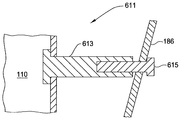
도 6은 본 발명의 일 실시예에 따른 콜리메이터를 PVD 챔버의 상부 실드에 부착시키는 브라켓의 확장된 부분 단면도이다.
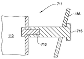
도 7은 본 발명의 일 실시예에 따른 콜리메이터를 PVD 챔버의 상부 실드에 부착시키기 위한 브라켓의 확장된 부분 단면도이다.
도 8은 본 발명의 일 실시예에 따른 모놀리식(monolithic) 콜리메이터를 상부에서 바라본 개략적인 도면이다.BRIEF DESCRIPTION OF DRAWINGS In order that the features of the present invention described above may be understood in detail, a more detailed description of the invention briefly summarized above is made with reference to the embodiments, some of which are illustrated in the accompanying drawings. However, the accompanying drawings show only typical embodiments of the invention, and the invention is to be regarded as limiting the scope of the invention as it allows for other equivalent embodiments.
1A and 1B are schematic cross-sectional views of a physical vapor deposition (PVD) chamber in accordance with embodiments of the present invention.
Figure 2 is a plan view of the collimator according to an embodiment of the present invention from the top surface.
3 is a schematic cross-sectional view of a collimator according to an embodiment of the present invention.
4 is a schematic cross-sectional view of a collimator according to an embodiment of the present invention.
5 is a schematic cross-sectional view of a collimator according to an embodiment of the present invention.
6 is an enlarged partial cross-sectional view of a bracket for attaching a collimator to an upper shield of a PVD chamber in accordance with one embodiment of the present invention.
7 is an enlarged partial cross-sectional view of a bracket for attaching a collimator to an upper shield of a PVD chamber in accordance with one embodiment of the present invention.
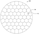
8 is a schematic view from above of a monolithic collimator in accordance with an embodiment of the present invention.
본 발명의 실시예들은 기판 상에 집적 회로를 조립하는 동안 기판의 높은 종횡비를 가지는 미세구조 전역에 스퍼터링 물질을 균일하게 증착시키기 위한 기구 및 방법을 제공한다.Embodiments of the present invention provide an apparatus and method for uniformly depositing sputtering material throughout a high aspect ratio microstructure of a substrate during assembly of an integrated circuit on the substrate.
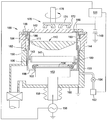
도 1a 및 도 1b는 본 발명의 실시예들에 따른 물리 기상 증착(physical vapor depostion; PVD) 챔버의 개략적인 단면을 나타내는 도면이다. PVD 챔버(100)는 타겟(142) 같은 스퍼터링 소스, 및 그 위에 반도체 기판(154)을 수용하기 위한 기판 지지 페데스탈(152)을 포함한다. 기판 지지 페데스탈은 접지된 챔버 벽(150) 내에 위치될 수 있다.1A and 1B are schematic cross-sectional views of a physical vapor deposition (PVD) chamber in accordance with embodiments of the present invention. The
일 실시예에서, 챔버(100)는 유전성 절연체(146)를 통하여 접지된 전도성 어댑터(144)에 의하여 지지되는 타겟(142)을 포함한다. 타겟(142)은 스퍼터링 동안 기판(154) 표면 상에 증착되는 물질을 포함하며, 기판(154) 내에 형성되는 높은 종횡비의 미세 구조물 내의 시드층으로서 형성되는 구리를 포함할 수 있다. 일 실시예에서, 타겟(142)은 또한 구리 같은 스퍼터링 가능한 물질로 이루어진 금속성 표면층, 및 알루미늄 같은 구조적 물질로 이루어진 후면층의 접합 합성물을 포함할 수 있다.In one embodiment,
일 실시예에서, 페데스탈(152)은 스퍼터링 코팅된 높은 종횡비의 미세 구조물을 구비하는 기판(154)을 지지하며, 상기 기판의 바닥은 타겟(142)의 주요 표면과 2차원적으로 반대 위치에 있다. 기판 지지 페데스탈(152)은 타겟(142)의 스퍼터링 표면과 대체로 평행하게 배치되는 2차원의 기판 수용 표면을 구비한다. 챔버(100)의 하부 부분 내의 로드 락 밸브(도시되지 않음)를 통하여 기판이 페데스탈(152) 상으로 운반될 수 있도록, 페데스탈(152)은 바닥 챔버 벽(160)과 연결된 벨로우(bellows; 158)를 통하여 수직으로 이동 가능할 수 있다. 이후에 페데스탈(152)은 도시된 바와 같은 증착 위치로 상승될 수 있다.In one embodiment,
일 실시예에서, 공정 가스는 가스 소스(162)로부터 질량 유동 제어부(164)를 통하여 챔버의 하부 부분 안으로 공급될 수 있다. 일 실시예에서, 챔버(100)와 결합된 제어 가능한 직류(DC) 전력 소스(158)가 타겟(152)에 음의 전압 또는 바이어스를 인가하기 위하여 이용될 수 있다. 라디오 주파수(RF) 전력 소스(156)가 기판(154) 상에 DC 자가-바이어스를 유도하기 위하여 페데스탈(152)에 결합될 수 있다. 일 실시예에서, 페데스탈(152)은 접지된다. 일 실시예에서, 페데스탈(152)은 전기적으로 플로팅된다(floated).In one embodiment, process gas may be supplied from the
일 실시예에서, 마그네트론(170)이 타겟(142) 상부에 위치된다. 마그네트론(170)은, 챔버(100) 및 기판(154)의 중심축을 따라서 축 방향으로 정렬될 수 있는, 샤프트(176)에 연결된 베이스 플레이트(174)에 의하여 지지되는 다수의 자석들(172)을 포함할 수 있다. 일 실시예에서, 자석들은 신장-모양의(kidney) 패턴으로 정렬된다. 타겟 물질의 스퍼터링 방출을 유도하게끔 매우 많은 이온 플럭스(flux)가 타겟(142)을 때리도록, 자석들(172)은 챔버(100) 내부의 타겟(142)의 전면 부근에 자기장을 유도하여 플라즈마를 생성한다. 타겟(142)의 표면 전역에서 자기장의 균일성을 증가시키기 위하여, 자석들(172)은 샤프트(176) 주위에서 회전될 수 있다. 일 실시예에서, 마그네트론은 작은 자석 마그네트론이다. 일 실시예에서, 나선형 운동이 이루어지도록, 자석들(172)은 타겟(142)의 표면에 실질적으로 평행인 선형 방향으로 왕복 이동되면서 왕복 회전될 수 있다. 일 실시예에서, 자석들(172)의 방사상(radial) 위치와 각(angular) 위치 모두를 제어하기 위하여, 자석들(172)은 중심축과 독립적으로 제어되는 2차 축 모두의 둘레로 회전될 수 있다. In one embodiment,
일 실시예에서, 챔버(100)는 챔버 측벽(150)에 의하여 지지되며 챔버 측벽(150)에 전기적으로 결합되는 상부 플랜지(182)를 구비하는 접지된 하부 실드(shield; 180)를 포함할 수 있다. 상부 실드(186)는 어댑터(144)의 플랜지(184)에 의하여 지지되며 어댑터(144)의 플랜지(184)에 전기적으로 결합된다. 상부 실드(186) 및 하부 실드(180)는 어댑터(144) 및 챔버 벽(150)과 마찬가지로 전기적으로 결합된다. 일 실시예에서, 상부 실드(186) 및 하부 실드(180) 각각은 알루미늄, 구리 및 스테인리스 스틸로부터 선택되는 물질로 이루어질 수 있다. 일 실시예에서, 챔버(100)는 상부 실드(186)와 결합되는 중앙 실드(도시되지 않음)를 포함한다. 일 실시예에서, 상부 실드(186) 및 하부 실드(180)는 챔버(100) 내부에서 전기적으로 플로팅된다. 일 실시예에서, 상부 실드(186) 및 하부 실드(180)는 전기적 전력 소스와 결합된다.In one embodiment, the
일 실시예에서, 상부 실드(186)는 상부 실드(186)와 타겟(142) 사이에 좁은 갭(188)을 형성하면서 타겟(142)의 환형 면 리세스(annular side recess)에 꼭 맞게 설비되는 상부 부분을 갖는데, 상기 좁은 갭(188)은 플라즈마가 유전성 절연체(146)를 지나가거나 유전성 절연체(146)에 스퍼터링 코팅되는 것을 방지할 수 있을 만큼 충분히 좁다. 상부 실드(186)는 또한 아래쪽으로 돌출된 팁(190)을 포함할 수 있는데, 상기 팁(190)은 하부 실드(180)와 상부 실드(186) 사이의 계면을 커버하며, 이에 따라 하부 실드(180)와 상부 실드(186)가 스퍼터링 증착된 물질에 의하여 접합되는 것이 방지된다.In one embodiment, the
일 실시예에서, 하부 실드(180)는, 대체로 챔버 벽(150)을 따라서 페데스탈(152)의 상면 아래로 연장하는 관형부(196) 내에서 아래쪽으로 연장한다. 하부 실드(180)는 튜브부(196)로부터 방사상 안쪽으로 연장하는 바닥부(198)를 구비할 수 있다. 바닥부(198)는 페데스탈(152)의 둘레를 둘러싸며 위쪽으로 연장하는 내부 립(103)을 포함할 수 있다. 일 실시예에서, 커버 링(102)은, 페데스탈(152)이 하부의 로딩 위치에 있을 때에는 립(103)의 상부에 놓여지며, 페데스탈(152)이 상부의 증착 위치에 있을 때에는 스퍼터링 물질로부터 페데스탈(152)을 보호하기 위하여 페데스탈(152)의 외부 주위에 놓여진다. In one embodiment, the
일 실시예에서, 타겟(142)과 기판 지지 페데스탈(152) 사이에 콜리메이터(110)를 위치시킴으로써 지향적인(directional) 스퍼터링이 달성될 수 있다. 도 1a에 도시된 바와 같이, 콜리메이터(110)는 다수의 방사 브라켓(11)을 매개로 상부 실드(186)와 기계적으로 그리고 전기적으로 결합될 수 있다. 일 실시예에서, 콜리메이터(110)는 챔버(100) 내부 하부에 위치되는 중앙 실드(도시되지 않음)와 결합된다. 일 실시예에서, 도 1b에 도시된 바와 같이, 콜리메이터(110)는 상부 실드(186)와 일체화된다. 일 실시예에서, 콜리메이터(110)는 상부 실드(186)에 용접된다. 일 실시예에서, 콜리메이터(110)는 챔버(110) 내부에서 전기적으로 플로팅될 수 있다. 일 실시예에서, 콜리메이터(110)는 전기적 전력 소스와 결합된다.In one embodiment, directional sputtering may be achieved by placing the
도 2는 일 실시예에 따른 콜리메이터(110)를 상면으로부터 관찰한 평면도이다. 콜리메이터(110)는 밀집한(close-packed) 배열 내의 육각형 개구(128)를 서로 구별시키는 육각형 벽(126)을 구비하는 대체로 벌집 형태인 구조물이다. 육각형 개구부(128)의 종횡비는 (콜리메이터의 두께와 동일한) 개구부(128)의 깊이를 개구부(128)의 폭으로서 나눈 값으로 정의될 수 있다. 일 실시예에서, 벽(126)의 두께는 약 0.06 인치에서 약 0.18 인치 사이이다. 일 실시예에서, 벽(126)의 두께는 약 0.12 인치에서 약 0.15 인치 사이이다. 일 실시예에서, 콜리메이터(110)는 알루미늄, 구리 및 스테인리스 스틸로부터 선택되는 물질로 이루어진다.2 is a plan view of the
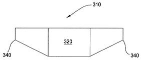
도 3은 본 발명의 일 실시예에 따른 콜리메이터(310)의 개략적인 단면도이다. 콜리메이터(310)는 약 1.5:1 내지 약 3:1 같은 높은 종횡비를 가지는 중앙 영역(320)을 포함한다. 일 실시예에서, 중앙 영역(320)의 종횡비는 약 2.5:1이다. 콜리메이터(310)의 종횡비는 중앙 영역(320)에서부터 주변 영역(340)까지 방사상 거리를 따라 감소한다. 일 실시예에서, 콜리메이터(310)의 종횡비는 중앙 영역(320)의 약 2.5:1의 종횡비에서 주변 영역(340)의 약 1:1의 종횡비로 감소한다. 다른 실시예에서, 콜리메이터(310)의 종횡비는 중앙 영역(320)의 약 3:1의 종횡비에서 주변 영역(340)의 약 1:1의 종횡비로 감소한다. 일 실시예에서, 콜리메이터(310)의 종횡비는 중앙 영역(320)의 약 1.5:1의 종횡비에서 주변 영역(340)의 약 1:1의 종횡비로 감소한다. 3 is a schematic cross-sectional view of a
일 실시예에서, 콜리메이터(310)의 두께를 다양화함으로써, 콜리메이터(310)의 방사 개구부를 감소시키는 것이 달성된다. 일 실시예에서, 콜리메이터(310)의 중앙 영역(320)은 약 3 인치 내지 약 6 인치 사이와 같은 증가된 두께를 가진다. 일 실시예에서, 콜리메이터(310)의 중앙 영역(320)은 약 5 인치이다. 일 실시예에서, 중앙 영역(320)에서부터 외부 주변 영역(340)까지 콜리메이터(310)의 두께가 감소한다. 일 실시예에서, 콜리메이터(310)의 두께는 중앙 영역(320)의 약 5 인치 두께에서 주변 영역(340)의 약 2 인치 두께로, 방사상으로 감소한다. 일 실시예에서, 콜리메이터(310)의 두께는 중앙 영역(320) 약 6 인치 두께에서 주변 영역(340)의 약 2 인치 두께로, 방사상으로 감소한다. 일 실시예에서, 콜리메이터(310)의 두께는 중앙 영역(320) 약 2.5 인치 두께에서 주변 영역(340)의 약 2 인치 두께로, 방사상으로 감소한다.In one embodiment, by varying the thickness of the
도 3에 묘사된 콜리메이터(310)의 실시예들의 종횡비의 변화가 방사상으로 두께가 감소하는 것으로 도시되고 있다 하더라도, 대안적으로, 종횡비는 콜리메이터(310)의 개구부 넓이를 증가시킴으로써 중앙 영역(320)에서부터 주변 영역(340)까지 감소될 수 있다. 다른 실시예에서, 중앙 영역(320)에서부터 주변 영역(340)까지, 콜리메이터(310)의 두께는 감소되며, 콜리메이터(310)의 개구부 넓이는 증가된다.Alternatively, although the change in aspect ratio of the embodiments of the
대체로, 도 3의 실시예들은 선형 방식으로 방사상으로 감소하는 것으로 묘사되고 있는데, 이는 역 삼각형 형상을 유발한다. 본 발명의 다른 실시예들은 종횡비가 비-선형적으로 감소하는 형태를 포함한다.In general, the embodiments of FIG. 3 are depicted as decreasing radially in a linear manner, which results in an inverted triangle shape. Other embodiments of the invention include forms in which the aspect ratio is non-linearly reduced.
도 4는 본 발명의 일 실시예에 따른 콜리메이터(410)의 개략적인 단면도이다. 콜리메이터(410)는 중앙 영역(420)에서부터 주변 영역(440)까지 비-선형 방식으로 감소하는 두께를 구비하는데, 이는 볼록한(convex) 형상을 유발한다.4 is a schematic cross-sectional view of a
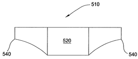
도 5는 본 발명의 일 실시예에 따른 콜리메이터(510)의 개략적인 단면도이다. 콜리메이터(510)는 중심 영역(520)에서부터 주변 영역(540)까지 비-선형 방식으로 감소하는 두께를 구비하는데, 이는 오목한(concave) 형상을 유발한다.5 is a schematic cross-sectional view of a
몇몇 실시예에서, 중심 영역(320, 420, 520)이 0(zero)에 접근하는데, 이는 중심 영역(320, 420, 520)이 콜리메이트(310, 410, 510)의 바닥에서 점으로 나타나도록 한다.In some embodiments,
도 1a 및 도 1b를 다시 참조하면, 콜리메이트(110)의 종횡비가 방사상으로 감소하는 어떠한 형상을 가진다 하더라도, PVD 챔버(100)의 작동과 콜리메이터(110)의 기능은 유사하다. 시스템 제어부(101)는 챔버(100)의 외부에 제공되며 대체로 전체 시스템의 제어 및 자동화를 촉진한다. 시스템 제어부(101)는 중앙 처리 유닛(central processing unit; CPU; 도시되지 않음), 메모리(도시되지 않음) 및 지지 회로(도시되지 않음)를 포함할 수 있다. CPU는 다양한 시스템 기능 및 챔버 공정을 제어하기 위하여 산업적으로 설치되어 이용되는 여느 컴퓨터 프로세서 중 하나일 수 있다.Referring again to FIGS. 1A and 1B, the operation of the
일 실시예에서, 시스템 제어부(101)는 기판 지지 페데스탈(152) 상에 기판을 위치시키기 위한 그리고 챔버(100) 내에 플라즈마를 생성하기 위한 신호를 제공한다. 타겟(142)에 바이어스를 걸기 위하여 그리고 아르곤 같은 공정 가스를 플라즈마 내부에 여기시키기(excite) 위하여, 시스템 제어부(101)는 DC 전력 소스(148)를 이용하여 전압을 인가하기 위한 신호를 보낸다. 시스템 제어부(101)는 또한 RF 전력 소스(156)로 하여금 페데스탈(152)에 DC 자가-바이어스를 걸게 하기 위한 신호를 제공할 수 있다. DC 자가-바이어스는 플라즈마 내에서 생성된 양으로 하전된 이온이 기판 표면 상의 높은 종횡비의 비아 및 트렌치 내로 강하게 유도되도록 하는데 도움을 줄 수 있다.In one embodiment,
콜리메이터(110)는 타겟(142)으로부터 기판(154)에 가까운 법선(normal)인, 선택된 각도를 초과하는 각도로 방출되는 이온 및 중성자를 붙잡기(trap) 위한 필터로서 기능한다. 콜리메이터(110)는 도 3 내지 도 5에 묘사된 각각의 콜리메이터(310, 410, 510) 중 하나일 수 있다. 중심으로부터 방사상으로 감소하는 종횡비를 가지는 콜리메이터(110)의 특성은, 타겟(142)의 주변 영역으로부터 방출되는 매우 높은 퍼센트의 이온이 콜리메이터(110)를 통하여 지나가도록 한다. 그 결과, 기판(154)의 주변 영역 상에 수많은 이온이 증가될 수 있으며, 기판(154)의 주변 영역 상에 증착되는 이온의 도달 각도 또한 증가될 수 있다. 따라서, 본 발명의 실시예들에 따르면, 물질은 더 균일하게 기판(154)의 표면 전역에 스퍼터링 증착될 수 있다. 추가적으로, 물질은 높은 종횡비를 가지는 미세 구조의 측벽 및 바닥 상에, 특히 기판(154) 주변 부근에 위치되는 높은 종횡비를 가지는 비아 및 트렌치 상에 더 균일하게 증착될 수 있다.The
추가적으로, 높은 종횡비를 가지는 미세구조의 바닥 및 측벽 상으로 스퍼터링 증착되는 물질에 매우 높은 커버리지를 제공하기 위하여, 미세구조의 필드(field) 및 바닥 영역 상에 스퍼터링 증착되는 물질은 스퍼터링 에칭될 수 있다. 일 실시예에서, 시스템 제어부(101)는 페데스탈(152)에 높은 바이어스를 공급하여 타겟(142) 이온이 기판(152) 상에 이미 증착된 막을 에칭하도록 한다. 그 결과, 기판(152) 상에의 필드 증착 속도는 감소되며, 높은 종횡비를 가지는 미세구조의 바닥 또는 측벽에 스퍼터링 물질이 재증착된다. 일 실시예에서, 시스템 제어부(101)는 높고 낮은 바이어스를 펄싱(pulsing) 또는 교대(alternating) 방식으로 페데스탈(152)에 공급하여, 공정이 펄싱 증착/에칭 공정이 되도록 한다. 일 실시예에서, 구체적으로 자석들(172)의 아래에 위치되는 콜리메이터(110) 셀은 대다수 증착 물질이 기판(154)의 방향으로 향하게 하도록 한다. 따라서, 여느 특별한 시기에, 기판의 일 영역 내에 물질이 증착될 수 있는 반면 이미 기판(154)의 다른 영역에 증착된 물질은 에칭된다.Additionally, in order to provide very high coverage for the material to be sputter deposited onto the bottom and sidewalls of the high aspect ratio microstructure, the material to be sputter deposited onto the field and bottom regions of the microstructure can be sputter etched. In one embodiment,
일 실시예에서, 높은 종횡비를 가지는 미세구조의 측벽 상에 스퍼터링 증착되는 물질로 더 높은 커버리지가 제공되도록, 미세구조의 바닥 상에 스퍼터링 증착되는 물질은, 기판(154) 부근의 챔버(100) 내의 영역에서 생성된, 아르곤 플라즈마 같은 2차 플라즈마를 이용하여 에칭될 수 있다. 일 실시예에서, 챔버(100)는 하부 실드(180)로부터 코일(141)을 전기적으로 절연시키는 다수의 코일 스탠드오프(standoff; 143)에 의하여 하부 실드(180)에 부착된 RF 코일(141)을 포함한다. 시스템 제어부(101)는 실드(180)를 통하여 피드스루(feedthrough) 스탠드오프(도시되지 않음)를 이용하여 RF 전력을 공급하기 위한 신호를 코일(141)에 보낸다. 일 실시예에서, RF 코일은 챔버(100) 안쪽의 RF 에너지와 유도적으로 결합하여, 기판(154) 부근의 2차 플라즈마가 유지되도록 아르곤 같은 프리커서 가스를 이온화시킨다. 2차 플라즈마는 높은 종횡비를 가지는 미세구조의 바닥으로부터 증착 층을 재스퍼터링하고 미세구조의 측면 상에 물질을 재증착한다.In one embodiment, the sputter deposited material on the bottom of the microstructure is in the
도 1a를 참조하면, 콜리메이터(110)는 다수의 방사 브라켓(11)에 의하여 상부 실드(186)에 부착될 수 있다. 도 6은 본 발명의 일 실시예에 따른 콜리메이터(110)를 상부 실드(186)에 부착시키는 브라켓(611)의 확장된 단면도이다. 브라켓(611)은 콜리메이터(110)에 용접되며 거기서부터 외부로 방사상으로 연장하는 내부적으로 돌출된 튜브(613)를 포함한다. 스크류 같은 조임 부재(fastening member; 615)가 상부 실드(186) 내의 개구를 통하여 삽입될 수 있으며, 콜리메이터(110)를 상부 실드(186)에 부착시키기 위하여 튜브(613) 내로 돌출될 수 있는 반면, 튜브(613) 또는 조임 부재(615)의 돌출된 부분 상으로 물질이 증착할 잠재적 가능성은 최소화된다.Referring to FIG. 1A, the
도 7은 본 발명의 일 실시예에 따른 콜리메이터(110)를 상부 실드(186)에 부착시키기 위한 브라켓(711)의 확장된 단면도이다. 브라켓(711)은 콜리메이터(110)와 용접되는 그곳에서부터 외부로 방사상으로 확대되는 스터드(713)를 포함한다. 내부적으로 돌출된 조임 부재(715)는, 상부 실드(186) 내의 개구를 통하여 삽입될 수 있으며, 콜리메이터(110)를 상부 실드(186)에 부착시키기 위한 스터드(713) 상에 돌출될 수 있는 반면, 스터드(713) 또는 조임 부재(715)의 돌출된 부분 상에 물질이 증착할 잠재적 가능성은 최소화된다.7 is an enlarged cross-sectional view of the
도 1b를 다시 참조하면, 콜리메이터(110)는 상부 실드(186)와 일체화될 수 있다. 도 8은 본 발명의 일 실시예에 따른 모놀리식(monolithic) 콜리메이터(800)를 상부에서 바라본 개략적인 도면이다. 이러한 실시예에서, 콜리메이터(110)는 상부 실드(186)와 일체화된다. 일 실시예에서, 용접 또는 다른 접합 기술을 이용하여, 콜리메이터(110)의 외부 가장자리(perimeter)는 상부 실드(186)의 내부 가장자리에 부착될 수 있다.Referring again to FIG. 1B, the
상술된 내용은 본 발명의 실시예들과 관련된 것이지만, 본 발명의 다른 또는 추가적인 실시예들이 본 발명의 기본적인 목적을 벗어나지 않는 범위 내에서 고안될 수 있으며, 본 발명의 목적은 아래와 같은 청구항에 의하여 구현될 수 있다.
While the foregoing is related to embodiments of the present invention, other or additional embodiments of the present invention may be devised without departing from the basic object thereof, and the object of the present invention may be embodied by the following claims. Can be.
Claims (15)
전기적으로 접지된 챔버;
상기 챔버에 의하여 지지되며 상기 챔버로부터 전기적으로 격리된(isolated) 스퍼터링 타겟;
상기 스퍼터링 타겟 아래에 위치되며 상기 스퍼티링 타겟의 스퍼터링 표면과 실질적으로 평행인 기판 지지 표면을 구비하는 기판 지지 페데스탈(pedestal);
상기 챔버에 의하여 지지되는 실드(shield) 부재; 및
상기 실드 부재와 기계적으로 그리고 전기적으로 결합되며 상기 기판 지지 페데스탈과 상기 스퍼터링 타겟 사이에 위치되는 콜리메이터(collimator)
를 포함하며,
상기 콜리메이터는 상기 콜리메이터를 관통하여 연장하는 다수의 개구부를 구비하며, 중앙 지역 내에 위치되는 개구부는 주변 영역 내에 위치되는 개구부보다 높은 종횡비를 가지는 증착 장치.As a vapor deposition apparatus,
An electrically grounded chamber;
A sputtering target supported by the chamber and electrically isolated from the chamber;
A substrate support pedestal positioned below the sputtering target and having a substrate support surface substantially parallel to the sputtering surface of the sputtering target;
A shield member supported by the chamber; And
A collimator mechanically and electrically coupled with the shield member and positioned between the substrate support pedestal and the sputtering target
Including;
The collimator having a plurality of openings extending through the collimator, wherein the opening located in the central region has a higher aspect ratio than the opening located in the peripheral region.
상기 개구부의 종횡비는 상기 중심 영역에서부터 상기 주변 영역까지 연속적으로 감소하는 증착 장치.The method of claim 1,
And the aspect ratio of the opening is continuously reduced from the center region to the peripheral region.
상기 콜리메이터의 두께는 상기 중심 영역에서부터 상기 주변 영역까지 연속적으로 감소하는 증착 장치.The method of claim 2,
And the thickness of the collimator continuously decreases from the central region to the peripheral region.
상기 개구부의 종횡비는 상기 중심 영역에서부터 상기 주변 영역까지 비선형적으로 감소하는 증착 장치.The method of claim 1,
And the aspect ratio of the opening decreases nonlinearly from the center region to the peripheral region.
상기 콜리메이터의 두께는 상기 중심 영역에서부터 상기 주변 영역까지 비선형적으로 감소하는 증착 장치.The method of claim 4, wherein
And the thickness of the collimator decreases nonlinearly from the central region to the peripheral region.
상기 콜리메이터는 브라켓을 이용하여 상기 실드 부재와 결합되며,
상기 브라켓은,
외부로 스레드된(threaded) 부재; 및
상기 외부로 스레드된 부재와 맞물리는 내부로 스레드된 부재
를 포함하는 증착 장치.The method of claim 1,
The collimator is coupled to the shield member using a bracket,
The bracket,
Externally threaded members; And
An internally threaded member engaged with the externally threaded member
Deposition apparatus comprising a.
상기 콜리메이터는 상기 실드 부재와 용접되는 증착 장치.The method of claim 1,
And the collimator is welded to the shield member.
상기 콜리메이터는 상기 실드 부재와 일체화되는 증착 장치.The method of claim 1,
And the collimator is integrated with the shield member.
상기 콜리메이터는 알루미늄, 구리 및 스테인리스 스틸로 이루어진 그룹으로부터 선택되는 물질로 구성되는 증착 장치.The method of claim 1,
And the collimator is comprised of a material selected from the group consisting of aluminum, copper and stainless steel.
상기 콜리메이터의 상기 개구부들 사이의 벽 두께는 약 0.06 인치 내지 약 0.18 인치 사이인 증착 장치.The method of claim 1,
And a wall thickness between the openings of the collimator is between about 0.06 inches and about 0.18 inches.
전기적으로 접지된 챔버;
상기 챔버에 의하여 지지되며 상기 챔버로부터 전기적으로 격리되고 DC 전력 소스와 전기적으로 결합되는 스퍼터링 타겟;
상기 스퍼터링 타겟 아래에 위치되며 상기 스퍼터링 타겟의 스퍼터링 표면과 실질적으로 평행한 기판 표면을 구비하고 RF 전력 소스와 전기적으로 결합되는 기판 지지 페데스탈;
상기 챔버에 의하여 지지되며 상기 챔버와 전기적으로 결합되는 실드 부재;
상기 실드 부재와 기계적으로 그리고 전기적으로 결합되며 상기 기판 지지 페데스탈과 상기 스퍼터링 타겟 사이에 위치되는 콜리메이터(collimator) - 상기 콜리메이터는 상기 콜리메이터를 관통하여 연장하는 다수의 개구부를 구비하며, 중앙 지역 내에 위치되는 개구부는 주변 영역 내에 위치되는 개구부보다 높은 종횡비를 가짐 -;
가스 소스; 및
상기 가스 소스, 상기 DC 전력 소스 및 상기 RF 전력 소스를 제어하기 위한 신호를 제공하도록 프로그램되며, 상기 기판 지지 페데스탈에 높은 바이어스를 제공하도록 프로그램된 제어부
를 포함하는 증착 장치. As a vapor deposition apparatus,
An electrically grounded chamber;
A sputtering target supported by the chamber and electrically isolated from the chamber and electrically coupled with a DC power source;
A substrate support pedestal positioned below the sputtering target and having a substrate surface substantially parallel to the sputtering surface of the sputtering target and electrically coupled with an RF power source;
A shield member supported by the chamber and electrically coupled to the chamber;
A collimator mechanically and electrically coupled to the shield member and positioned between the substrate support pedestal and the sputtering target, the collimator having a plurality of openings extending through the collimator, the collimator being located within a central area The opening has a higher aspect ratio than the opening located in the peripheral region;
Gas source; And
A controller programmed to provide a signal for controlling the gas source, the DC power source and the RF power source, the controller programmed to provide a high bias to the substrate support pedestal
Deposition apparatus comprising a.
RF 코일을 더 포함하고,
상기 제어부는 상기 기판 지지 페데스탈이 높고 낮은 바이어스 사이에서 교대되게끔 상기 RF 전력 소스를 제어하기 위한 신호를 제공하도록 프로그램되며, 상기 제어부는 상기 챔버 내의 2차 플라즈마를 제어하기 위하여 RF 코일 및 상기 가스 소스에 제공되는 전력을 제어하도록 프로그램된 증착 장치.The method of claim 11,
Further includes an RF coil,
The controller is programmed to provide a signal for controlling the RF power source such that the substrate support pedestal alternates between a high and low bias, the controller being configured to control the RF coil and the gas source to control a secondary plasma in the chamber. Deposition apparatus programmed to control the power provided to the apparatus.
상기 콜리메이터의 두께는 상기 중심 영역에서부터 상기 주변 영역까지 연속적으로 감소하는 증착 장치.The method of claim 12,
And the thickness of the collimator continuously decreases from the central region to the peripheral region.
챔버 내부의 스퍼터링 타겟에 DC 바이어스를 인가하는 단계 - 상기 챔버는 상기 스퍼터링 타겟과 기판 지지 페데스탈 사이에 위치되는 콜리메이터를 구비하고, 상기 콜리메이터는 상기 콜리메이터를 관통하여 연장하는 다수의 개구부를 구비하며, 중앙 지역 내에 위치되는 개구부는 주변 영역 내에 위치되는 개구부보다 높은 종횡비를 가짐 -;
상기 챔버 내부의 상기 스퍼터링 타겟에 인접한 영역에 공정 가스를 제공하는 단계;
상기 기판 지지 페데스탈에 바이어스를 인가하는 단계; 및
상기 기판 지지 페데스탈에 인가되는 바이어스를 높은 바이어스와 낮은 바이어스 사이로 펄싱(pulsing)하는 단계
를 포함하는 기판 상에 물질을 증착하기 위한 방법.A method for depositing a material on a substrate,
Applying a DC bias to the sputtering target inside the chamber, the chamber having a collimator positioned between the sputtering target and the substrate support pedestal, the collimator having a plurality of openings extending through the collimator, the center of The opening located within the region has a higher aspect ratio than the opening located within the peripheral region;
Providing a process gas to an area adjacent said sputtering target within said chamber;
Applying a bias to the substrate support pedestal; And
Pulsing a bias applied to the substrate support pedestal between a high bias and a low bias
A method for depositing a material on a substrate comprising a.
상기 챔버 내부에 2차 플라즈마를 제공하기 위하여 상기 챔버 내부에 위치되는 RF 코일에 전력을 인가하는 단계를 더 포함하며,
상기 개구부의 종횡비는 상기 중심 영역에서부터 상기 주변 영역까지 연속적으로 감소하는 기판 상에 물질을 증착하기 위한 방법.
The method of claim 14,
Applying power to an RF coil located inside the chamber to provide a secondary plasma inside the chamber,
And the aspect ratio of the opening decreases continuously from the central region to the peripheral region.
Applications Claiming Priority (2)
| Application Number | Priority Date | Filing Date | Title |
|---|---|---|---|
| US7313008P | 2008-06-17 | 2008-06-17 | |
| US61/073,130 | 2008-06-17 |
Related Child Applications (2)
| Application Number | Title | Priority Date | Filing Date |
|---|---|---|---|
| KR1020157033650A Division KR20150137131A (en) | 2008-06-17 | 2009-06-11 | Apparatus and method for uniform deposition |
| KR1020167034645A Division KR20160145849A (en) | 2008-06-17 | 2009-06-11 | Apparatus and method for uniform deposition |
Publications (1)
| Publication Number | Publication Date |
|---|---|
| KR20110020918A true KR20110020918A (en) | 2011-03-03 |
Family
ID=41413769
Family Applications (8)
| Application Number | Title | Priority Date | Filing Date |
|---|---|---|---|
| KR1020167034645A KR20160145849A (en) | 2008-06-17 | 2009-06-11 | Apparatus and method for uniform deposition |
| KR1020207021871A KR20200093084A (en) | 2008-06-17 | 2009-06-11 | Apparatus and method for uniform deposition |
| KR1020167031883A KR20160134873A (en) | 2008-06-17 | 2009-06-11 | Apparatus and method for uniform deposition |
| KR1020117001222A KR20110020918A (en) | 2008-06-17 | 2009-06-11 | Apparatus and method for uniform deposition |
| KR1020187004305A KR20180019762A (en) | 2008-06-17 | 2009-06-11 | Apparatus and method for uniform deposition |
| KR1020197023662A KR20190097315A (en) | 2008-06-17 | 2009-06-11 | Apparatus and method for uniform deposition |
| KR1020157033650A KR20150137131A (en) | 2008-06-17 | 2009-06-11 | Apparatus and method for uniform deposition |
| KR1020177023703A KR20170100068A (en) | 2008-06-17 | 2009-06-11 | Apparatus and method for uniform deposition |
Family Applications Before (3)
| Application Number | Title | Priority Date | Filing Date |
|---|---|---|---|
| KR1020167034645A KR20160145849A (en) | 2008-06-17 | 2009-06-11 | Apparatus and method for uniform deposition |
| KR1020207021871A KR20200093084A (en) | 2008-06-17 | 2009-06-11 | Apparatus and method for uniform deposition |
| KR1020167031883A KR20160134873A (en) | 2008-06-17 | 2009-06-11 | Apparatus and method for uniform deposition |
Family Applications After (4)
| Application Number | Title | Priority Date | Filing Date |
|---|---|---|---|
| KR1020187004305A KR20180019762A (en) | 2008-06-17 | 2009-06-11 | Apparatus and method for uniform deposition |
| KR1020197023662A KR20190097315A (en) | 2008-06-17 | 2009-06-11 | Apparatus and method for uniform deposition |
| KR1020157033650A KR20150137131A (en) | 2008-06-17 | 2009-06-11 | Apparatus and method for uniform deposition |
| KR1020177023703A KR20170100068A (en) | 2008-06-17 | 2009-06-11 | Apparatus and method for uniform deposition |
Country Status (5)
| Country | Link |
|---|---|
| US (1) | US20090308732A1 (en) |
| JP (1) | JP2011524471A (en) |
| KR (8) | KR20160145849A (en) |
| CN (1) | CN102066603B (en) |
| WO (1) | WO2009155208A2 (en) |
Cited By (3)
| Publication number | Priority date | Publication date | Assignee | Title |
|---|---|---|---|---|
| WO2013090532A1 (en) * | 2011-12-15 | 2013-06-20 | Applied Materials, Inc. | Apparatus for enabling concentricity of plasma dark space |
| WO2014039252A1 (en) * | 2012-09-05 | 2014-03-13 | Applied Materials, Inc. | Target center positional constraint for physical vapor deposition (pvd) processing systems |
| KR20170130347A (en) * | 2016-03-14 | 2017-11-28 | 가부시끼가이샤 도시바 | Processing apparatus and collimator |
Families Citing this family (23)
| Publication number | Priority date | Publication date | Assignee | Title |
|---|---|---|---|---|
| CN101845610B (en) * | 2010-06-07 | 2011-12-07 | 崔铮 | Continuous vertical hot evaporation metal film coating method |
| JP5825781B2 (en) * | 2010-12-17 | 2015-12-02 | キヤノン株式会社 | Antireflection film forming method and antireflection film forming apparatus |
| CN103165375B (en) * | 2011-12-09 | 2016-06-01 | 中国科学院微电子研究所 | Semiconductor chamber preforming device |
| US9404174B2 (en) | 2011-12-15 | 2016-08-02 | Applied Materials, Inc. | Pinned target design for RF capacitive coupled plasma |
| US9831074B2 (en) * | 2013-10-24 | 2017-11-28 | Applied Materials, Inc. | Bipolar collimator utilized in a physical vapor deposition chamber |
| US20150122643A1 (en) * | 2013-11-06 | 2015-05-07 | Shenzhen China Star Optoelectronics Technology Co., Ltd. | Supporting member for magnetron sputtering anode bar and magnetron sputtering device including the same |
| CN103602954B (en) * | 2013-11-06 | 2016-02-24 | 深圳市华星光电技术有限公司 | For magnetron sputtering anode bar strut member and comprise its magnetic control sputtering device |
| US9887072B2 (en) | 2014-01-23 | 2018-02-06 | Taiwan Semiconductor Manufacturing Company, Ltd. | Systems and methods for integrated resputtering in a physical vapor deposition chamber |
| US20170182556A1 (en) * | 2014-07-18 | 2017-06-29 | Applied Materials, Inc. | Additive manufacturing with laser and gas flow |
| US9543126B2 (en) * | 2014-11-26 | 2017-01-10 | Applied Materials, Inc. | Collimator for use in substrate processing chambers |
| US9887073B2 (en) * | 2015-02-13 | 2018-02-06 | Taiwan Semiconductor Manufacturing Co., Ltd. | Physical vapor deposition system and physical vapor depositing method using the same |
| US9960024B2 (en) | 2015-10-27 | 2018-05-01 | Applied Materials, Inc. | Biasable flux optimizer / collimator for PVD sputter chamber |
| CN112599401B (en) * | 2016-03-05 | 2024-03-22 | 应用材料公司 | Method and apparatus for controlling ion fraction in a physical vapor deposition process |
| USD859333S1 (en) * | 2018-03-16 | 2019-09-10 | Applied Materials, Inc. | Collimator for a physical vapor deposition chamber |
| USD858468S1 (en) * | 2018-03-16 | 2019-09-03 | Applied Materials, Inc. | Collimator for a physical vapor deposition chamber |
| US11017989B2 (en) | 2018-03-16 | 2021-05-25 | Samsung Electronics Co., Ltd. | Collimator, fabrication apparatus including the same, and method of fabricating a semiconductor device using the same |
| CN110643958A (en) * | 2019-10-21 | 2020-01-03 | 吴浪生 | Physical coating equipment for realizing wafer by sputtering |
| USD937329S1 (en) | 2020-03-23 | 2021-11-30 | Applied Materials, Inc. | Sputter target for a physical vapor deposition chamber |
| USD998575S1 (en) | 2020-04-07 | 2023-09-12 | Applied Materials, Inc. | Collimator for use in a physical vapor deposition (PVD) chamber |
| US20220406583A1 (en) * | 2021-06-18 | 2022-12-22 | Taiwan Semiconductor Manufacturing Co., Ltd. | Deposition system and method |
| USD1009816S1 (en) | 2021-08-29 | 2024-01-02 | Applied Materials, Inc. | Collimator for a physical vapor deposition chamber |
| USD997111S1 (en) | 2021-12-15 | 2023-08-29 | Applied Materials, Inc. | Collimator for use in a physical vapor deposition (PVD) chamber |
| FI20225334A1 (en) * | 2022-04-21 | 2023-10-22 | Biomensio Ltd | Collimator for Production of Piezoelectric Layers with Tilted c-Axis Orientation |
Family Cites Families (21)
| Publication number | Priority date | Publication date | Assignee | Title |
|---|---|---|---|---|
| US5362372A (en) * | 1993-06-11 | 1994-11-08 | Applied Materials, Inc. | Self cleaning collimator |
| US5380414A (en) * | 1993-06-11 | 1995-01-10 | Applied Materials, Inc. | Shield and collimator pasting deposition chamber with a wafer support periodically used as an acceptor |
| US5415753A (en) * | 1993-07-22 | 1995-05-16 | Materials Research Corporation | Stationary aperture plate for reactive sputter deposition |
| US5431799A (en) * | 1993-10-29 | 1995-07-11 | Applied Materials, Inc. | Collimation hardware with RF bias rings to enhance sputter and/or substrate cavity ion generation efficiency |
| US5650052A (en) * | 1995-10-04 | 1997-07-22 | Edelstein; Sergio | Variable cell size collimator |
| US5985102A (en) * | 1996-01-29 | 1999-11-16 | Micron Technology, Inc. | Kit for electrically isolating collimator of PVD chamber, chamber so modified, and method of using |
| US5658442A (en) * | 1996-03-07 | 1997-08-19 | Applied Materials, Inc. | Target and dark space shield for a physical vapor deposition system |
| JPH10176267A (en) * | 1996-12-13 | 1998-06-30 | Applied Materials Inc | Sputtering device |
| US6692617B1 (en) * | 1997-05-08 | 2004-02-17 | Applied Materials, Inc. | Sustained self-sputtering reactor having an increased density plasma |
| US6482301B1 (en) * | 1998-06-04 | 2002-11-19 | Seagate Technology, Inc. | Target shields for improved magnetic properties of a recording medium |
| US6149776A (en) * | 1998-11-12 | 2000-11-21 | Applied Materials, Inc. | Copper sputtering target |
| KR20000052104A (en) * | 1999-01-29 | 2000-08-16 | 윤종용 | Collimator structure and its manufacturing method in sputtering apparatus |
| US20030116427A1 (en) * | 2001-08-30 | 2003-06-26 | Applied Materials, Inc. | Self-ionized and inductively-coupled plasma for sputtering and resputtering |
| US6699375B1 (en) * | 2000-06-29 | 2004-03-02 | Applied Materials, Inc. | Method of extending process kit consumable recycling life |
| US20030015421A1 (en) * | 2001-07-20 | 2003-01-23 | Applied Materials, Inc. | Collimated sputtering of cobalt |
| US20030029715A1 (en) * | 2001-07-25 | 2003-02-13 | Applied Materials, Inc. | An Apparatus For Annealing Substrates In Physical Vapor Deposition Systems |
| US7041200B2 (en) * | 2002-04-19 | 2006-05-09 | Applied Materials, Inc. | Reducing particle generation during sputter deposition |
| US7048837B2 (en) * | 2002-09-13 | 2006-05-23 | Applied Materials, Inc. | End point detection for sputtering and resputtering |
| TW200416838A (en) * | 2002-11-20 | 2004-09-01 | Renesas Tech Corp | Method of fabricating semiconductor device |
| US7018515B2 (en) * | 2004-03-24 | 2006-03-28 | Applied Materials, Inc. | Selectable dual position magnetron |
| JP2007273490A (en) * | 2004-03-30 | 2007-10-18 | Renesas Technology Corp | Method of manufacturing semiconductor integrated circuit device |
-
2009
- 2009-06-11 KR KR1020167034645A patent/KR20160145849A/en not_active Application Discontinuation
- 2009-06-11 KR KR1020207021871A patent/KR20200093084A/en not_active Application Discontinuation
- 2009-06-11 KR KR1020167031883A patent/KR20160134873A/en not_active Application Discontinuation
- 2009-06-11 CN CN2009801229458A patent/CN102066603B/en active Active
- 2009-06-11 KR KR1020117001222A patent/KR20110020918A/en not_active Application Discontinuation
- 2009-06-11 JP JP2011514713A patent/JP2011524471A/en active Pending
- 2009-06-11 WO PCT/US2009/047103 patent/WO2009155208A2/en active Application Filing
- 2009-06-11 KR KR1020187004305A patent/KR20180019762A/en active Search and Examination
- 2009-06-11 KR KR1020197023662A patent/KR20190097315A/en not_active Application Discontinuation
- 2009-06-11 US US12/482,713 patent/US20090308732A1/en not_active Abandoned
- 2009-06-11 KR KR1020157033650A patent/KR20150137131A/en not_active Application Discontinuation
- 2009-06-11 KR KR1020177023703A patent/KR20170100068A/en not_active Application Discontinuation
Cited By (3)
| Publication number | Priority date | Publication date | Assignee | Title |
|---|---|---|---|---|
| WO2013090532A1 (en) * | 2011-12-15 | 2013-06-20 | Applied Materials, Inc. | Apparatus for enabling concentricity of plasma dark space |
| WO2014039252A1 (en) * | 2012-09-05 | 2014-03-13 | Applied Materials, Inc. | Target center positional constraint for physical vapor deposition (pvd) processing systems |
| KR20170130347A (en) * | 2016-03-14 | 2017-11-28 | 가부시끼가이샤 도시바 | Processing apparatus and collimator |
Also Published As
| Publication number | Publication date |
|---|---|
| KR20150137131A (en) | 2015-12-08 |
| KR20200093084A (en) | 2020-08-04 |
| KR20160134873A (en) | 2016-11-23 |
| WO2009155208A3 (en) | 2010-03-18 |
| KR20160145849A (en) | 2016-12-20 |
| JP2011524471A (en) | 2011-09-01 |
| CN102066603A (en) | 2011-05-18 |
| KR20180019762A (en) | 2018-02-26 |
| CN102066603B (en) | 2013-04-10 |
| US20090308732A1 (en) | 2009-12-17 |
| WO2009155208A2 (en) | 2009-12-23 |
| KR20190097315A (en) | 2019-08-20 |
| KR20170100068A (en) | 2017-09-01 |
Similar Documents
| Publication | Publication Date | Title |
|---|---|---|
| KR20110020918A (en) | Apparatus and method for uniform deposition | |
| CN107002220B (en) | Collimator for use in a substrate processing chamber | |
| KR102020010B1 (en) | Wafer processing deposition shielding components | |
| US20090308739A1 (en) | Wafer processing deposition shielding components | |
| JP2018533673A (en) | Biasable flux optimizer / collimator for PVD sputter chamber | |
| CN116752109A (en) | Physical vapor deposition equipment, deposition process and etching process |
Legal Events
| Date | Code | Title | Description |
|---|---|---|---|
| E902 | Notification of reason for refusal | ||
| A107 | Divisional application of patent | ||
| E90F | Notification of reason for final refusal | ||
| E601 | Decision to refuse application | ||
| E801 | Decision on dismissal of amendment | ||
| J201 | Request for trial against refusal decision | ||
| A107 | Divisional application of patent | ||
| WITB | Written withdrawal of application | ||
| J301 | Trial decision |
Free format text: TRIAL NUMBER: 2016101006542; TRIAL DECISION FOR APPEAL AGAINST DECISION TO DECLINE REFUSAL REQUESTED 20161118 Effective date: 20170113 |