KR20100122485A - System and method for emitter layer shaping - Google Patents
System and method for emitter layer shaping Download PDFInfo
- Publication number
- KR20100122485A KR20100122485A KR1020107018431A KR20107018431A KR20100122485A KR 20100122485 A KR20100122485 A KR 20100122485A KR 1020107018431 A KR1020107018431 A KR 1020107018431A KR 20107018431 A KR20107018431 A KR 20107018431A KR 20100122485 A KR20100122485 A KR 20100122485A
- Authority
- KR
- South Korea
- Prior art keywords
- light emitting
- light
- led
- area
- emitter
- Prior art date
Links
- 238000000034 method Methods 0.000 title claims abstract description 100
- 238000007493 shaping process Methods 0.000 title claims abstract description 55
- 239000000758 substrate Substances 0.000 claims abstract description 155
- 238000005530 etching Methods 0.000 claims abstract description 36
- 239000000463 material Substances 0.000 claims description 137
- JMASRVWKEDWRBT-UHFFFAOYSA-N Gallium nitride Chemical compound [Ga]#N JMASRVWKEDWRBT-UHFFFAOYSA-N 0.000 claims description 60
- 238000000605 extraction Methods 0.000 claims description 16
- HBMJWWWQQXIZIP-UHFFFAOYSA-N silicon carbide Chemical compound [Si+]#[C-] HBMJWWWQQXIZIP-UHFFFAOYSA-N 0.000 claims description 11
- 238000000059 patterning Methods 0.000 claims description 7
- 239000006117 anti-reflective coating Substances 0.000 claims description 5
- 230000008021 deposition Effects 0.000 claims description 5
- 230000005540 biological transmission Effects 0.000 claims description 4
- 229910018072 Al 2 O 3 Inorganic materials 0.000 claims 3
- TWNQGVIAIRXVLR-UHFFFAOYSA-N oxo(oxoalumanyloxy)alumane Chemical compound O=[Al]O[Al]=O TWNQGVIAIRXVLR-UHFFFAOYSA-N 0.000 claims 3
- 238000009826 distribution Methods 0.000 abstract description 17
- 239000000284 extract Substances 0.000 abstract description 3
- 239000010410 layer Substances 0.000 description 178
- 229910002601 GaN Inorganic materials 0.000 description 62
- 229910052594 sapphire Inorganic materials 0.000 description 34
- 239000010980 sapphire Substances 0.000 description 34
- 230000008569 process Effects 0.000 description 28
- 238000010586 diagram Methods 0.000 description 19
- 230000008901 benefit Effects 0.000 description 14
- 239000002245 particle Substances 0.000 description 14
- XLYOFNOQVPJJNP-UHFFFAOYSA-N water Substances O XLYOFNOQVPJJNP-UHFFFAOYSA-N 0.000 description 14
- 238000000151 deposition Methods 0.000 description 13
- 238000004519 manufacturing process Methods 0.000 description 13
- 239000000460 chlorine Substances 0.000 description 12
- 239000011248 coating agent Substances 0.000 description 12
- 238000000576 coating method Methods 0.000 description 12
- 229920002120 photoresistant polymer Polymers 0.000 description 12
- 239000007787 solid Substances 0.000 description 12
- 229910052751 metal Inorganic materials 0.000 description 10
- 239000002184 metal Substances 0.000 description 10
- 229910010271 silicon carbide Inorganic materials 0.000 description 8
- 230000003287 optical effect Effects 0.000 description 7
- 230000005855 radiation Effects 0.000 description 6
- 239000004065 semiconductor Substances 0.000 description 6
- OAICVXFJPJFONN-UHFFFAOYSA-N Phosphorus Chemical compound [P] OAICVXFJPJFONN-UHFFFAOYSA-N 0.000 description 5
- 230000008859 change Effects 0.000 description 5
- 238000011161 development Methods 0.000 description 5
- 230000018109 developmental process Effects 0.000 description 5
- 230000004907 flux Effects 0.000 description 5
- 239000007789 gas Substances 0.000 description 5
- 238000005286 illumination Methods 0.000 description 5
- 238000009616 inductively coupled plasma Methods 0.000 description 5
- 230000007480 spreading Effects 0.000 description 5
- 238000003892 spreading Methods 0.000 description 5
- 238000010521 absorption reaction Methods 0.000 description 4
- 150000001875 compounds Chemical class 0.000 description 4
- 238000001312 dry etching Methods 0.000 description 4
- 238000005516 engineering process Methods 0.000 description 4
- 230000017525 heat dissipation Effects 0.000 description 4
- KRHYYFGTRYWZRS-UHFFFAOYSA-N hydrofluoric acid Substances F KRHYYFGTRYWZRS-UHFFFAOYSA-N 0.000 description 4
- 230000006872 improvement Effects 0.000 description 4
- 238000000608 laser ablation Methods 0.000 description 4
- 210000002381 plasma Anatomy 0.000 description 4
- 238000001020 plasma etching Methods 0.000 description 4
- 238000004321 preservation Methods 0.000 description 4
- 230000007704 transition Effects 0.000 description 4
- 238000007792 addition Methods 0.000 description 3
- 210000004027 cell Anatomy 0.000 description 3
- 239000013078 crystal Substances 0.000 description 3
- 238000013461 design Methods 0.000 description 3
- 239000010432 diamond Substances 0.000 description 3
- 229910003460 diamond Inorganic materials 0.000 description 3
- 230000000694 effects Effects 0.000 description 3
- 239000008393 encapsulating agent Substances 0.000 description 3
- 239000011521 glass Substances 0.000 description 3
- 238000000227 grinding Methods 0.000 description 3
- 238000012986 modification Methods 0.000 description 3
- 230000004048 modification Effects 0.000 description 3
- 239000002105 nanoparticle Substances 0.000 description 3
- 238000004590 computer program Methods 0.000 description 2
- 238000009792 diffusion process Methods 0.000 description 2
- 230000005670 electromagnetic radiation Effects 0.000 description 2
- 239000007788 liquid Substances 0.000 description 2
- 238000001465 metallisation Methods 0.000 description 2
- 239000000203 mixture Substances 0.000 description 2
- QPJSUIGXIBEQAC-UHFFFAOYSA-N n-(2,4-dichloro-5-propan-2-yloxyphenyl)acetamide Chemical compound CC(C)OC1=CC(NC(C)=O)=C(Cl)C=C1Cl QPJSUIGXIBEQAC-UHFFFAOYSA-N 0.000 description 2
- 238000012545 processing Methods 0.000 description 2
- 239000000047 product Substances 0.000 description 2
- 239000000243 solution Substances 0.000 description 2
- 230000003746 surface roughness Effects 0.000 description 2
- 238000001039 wet etching Methods 0.000 description 2
- DDFHBQSCUXNBSA-UHFFFAOYSA-N 5-(5-carboxythiophen-2-yl)thiophene-2-carboxylic acid Chemical compound S1C(C(=O)O)=CC=C1C1=CC=C(C(O)=O)S1 DDFHBQSCUXNBSA-UHFFFAOYSA-N 0.000 description 1
- ZCYVEMRRCGMTRW-UHFFFAOYSA-N 7553-56-2 Chemical compound [I] ZCYVEMRRCGMTRW-UHFFFAOYSA-N 0.000 description 1
- 229910002704 AlGaN Inorganic materials 0.000 description 1
- ZAMOUSCENKQFHK-UHFFFAOYSA-N Chlorine atom Chemical compound [Cl] ZAMOUSCENKQFHK-UHFFFAOYSA-N 0.000 description 1
- UFHFLCQGNIYNRP-UHFFFAOYSA-N Hydrogen Chemical compound [H][H] UFHFLCQGNIYNRP-UHFFFAOYSA-N 0.000 description 1
- 229910018503 SF6 Inorganic materials 0.000 description 1
- 229910004298 SiO 2 Inorganic materials 0.000 description 1
- VYPSYNLAJGMNEJ-UHFFFAOYSA-N Silicium dioxide Chemical compound O=[Si]=O VYPSYNLAJGMNEJ-UHFFFAOYSA-N 0.000 description 1
- 239000003082 abrasive agent Substances 0.000 description 1
- 230000006978 adaptation Effects 0.000 description 1
- 238000004458 analytical method Methods 0.000 description 1
- 238000003491 array Methods 0.000 description 1
- 238000004364 calculation method Methods 0.000 description 1
- 238000001311 chemical methods and process Methods 0.000 description 1
- 238000006243 chemical reaction Methods 0.000 description 1
- 238000005229 chemical vapour deposition Methods 0.000 description 1
- 229910052801 chlorine Inorganic materials 0.000 description 1
- 239000003086 colorant Substances 0.000 description 1
- 238000012777 commercial manufacturing Methods 0.000 description 1
- 238000005094 computer simulation Methods 0.000 description 1
- 239000004020 conductor Substances 0.000 description 1
- 238000005520 cutting process Methods 0.000 description 1
- 238000009795 derivation Methods 0.000 description 1
- 238000005553 drilling Methods 0.000 description 1
- 238000004836 empirical method Methods 0.000 description 1
- 238000004134 energy conservation Methods 0.000 description 1
- 238000000407 epitaxy Methods 0.000 description 1
- 230000006870 function Effects 0.000 description 1
- 229910052736 halogen Inorganic materials 0.000 description 1
- 150000002367 halogens Chemical class 0.000 description 1
- 230000020169 heat generation Effects 0.000 description 1
- 229910052739 hydrogen Inorganic materials 0.000 description 1
- 239000001257 hydrogen Substances 0.000 description 1
- 230000006698 induction Effects 0.000 description 1
- 238000002347 injection Methods 0.000 description 1
- 239000007924 injection Substances 0.000 description 1
- 230000003993 interaction Effects 0.000 description 1
- 229910052740 iodine Inorganic materials 0.000 description 1
- 239000011630 iodine Substances 0.000 description 1
- 150000002500 ions Chemical class 0.000 description 1
- 239000004973 liquid crystal related substance Substances 0.000 description 1
- 229910001092 metal group alloy Inorganic materials 0.000 description 1
- 238000003801 milling Methods 0.000 description 1
- 229910003465 moissanite Inorganic materials 0.000 description 1
- 238000001451 molecular beam epitaxy Methods 0.000 description 1
- 239000003921 oil Substances 0.000 description 1
- 238000005457 optimization Methods 0.000 description 1
- 238000002161 passivation Methods 0.000 description 1
- 238000001259 photo etching Methods 0.000 description 1
- 239000004033 plastic Substances 0.000 description 1
- 238000005498 polishing Methods 0.000 description 1
- 229920000642 polymer Polymers 0.000 description 1
- 230000001902 propagating effect Effects 0.000 description 1
- 239000011241 protective layer Substances 0.000 description 1
- 230000008707 rearrangement Effects 0.000 description 1
- 238000004064 recycling Methods 0.000 description 1
- 238000005201 scrubbing Methods 0.000 description 1
- 238000000926 separation method Methods 0.000 description 1
- 229910052814 silicon oxide Inorganic materials 0.000 description 1
- 238000004088 simulation Methods 0.000 description 1
- 238000001228 spectrum Methods 0.000 description 1
- 239000007858 starting material Substances 0.000 description 1
- 239000000126 substance Substances 0.000 description 1
- 238000006467 substitution reaction Methods 0.000 description 1
- SFZCNBIFKDRMGX-UHFFFAOYSA-N sulfur hexafluoride Chemical compound FS(F)(F)(F)(F)F SFZCNBIFKDRMGX-UHFFFAOYSA-N 0.000 description 1
- 229960000909 sulfur hexafluoride Drugs 0.000 description 1
- 239000013589 supplement Substances 0.000 description 1
- 239000010409 thin film Substances 0.000 description 1
- 238000012546 transfer Methods 0.000 description 1
- FAQYAMRNWDIXMY-UHFFFAOYSA-N trichloroborane Chemical compound ClB(Cl)Cl FAQYAMRNWDIXMY-UHFFFAOYSA-N 0.000 description 1
- 238000009827 uniform distribution Methods 0.000 description 1
- 238000000927 vapour-phase epitaxy Methods 0.000 description 1
- 238000001947 vapour-phase growth Methods 0.000 description 1
Images


Classifications
-
- H—ELECTRICITY
- H01—ELECTRIC ELEMENTS
- H01L—SEMICONDUCTOR DEVICES NOT COVERED BY CLASS H10
- H01L33/00—Semiconductor devices having potential barriers specially adapted for light emission; Processes or apparatus specially adapted for the manufacture or treatment thereof or of parts thereof; Details thereof
- H01L33/02—Semiconductor devices having potential barriers specially adapted for light emission; Processes or apparatus specially adapted for the manufacture or treatment thereof or of parts thereof; Details thereof characterised by the semiconductor bodies
- H01L33/20—Semiconductor devices having potential barriers specially adapted for light emission; Processes or apparatus specially adapted for the manufacture or treatment thereof or of parts thereof; Details thereof characterised by the semiconductor bodies with a particular shape, e.g. curved or truncated substrate
-
- H—ELECTRICITY
- H01—ELECTRIC ELEMENTS
- H01L—SEMICONDUCTOR DEVICES NOT COVERED BY CLASS H10
- H01L33/00—Semiconductor devices having potential barriers specially adapted for light emission; Processes or apparatus specially adapted for the manufacture or treatment thereof or of parts thereof; Details thereof
- H01L33/02—Semiconductor devices having potential barriers specially adapted for light emission; Processes or apparatus specially adapted for the manufacture or treatment thereof or of parts thereof; Details thereof characterised by the semiconductor bodies
- H01L33/08—Semiconductor devices having potential barriers specially adapted for light emission; Processes or apparatus specially adapted for the manufacture or treatment thereof or of parts thereof; Details thereof characterised by the semiconductor bodies with a plurality of light emitting regions, e.g. laterally discontinuous light emitting layer or photoluminescent region integrated within the semiconductor body
-
- H—ELECTRICITY
- H01—ELECTRIC ELEMENTS
- H01L—SEMICONDUCTOR DEVICES NOT COVERED BY CLASS H10
- H01L33/00—Semiconductor devices having potential barriers specially adapted for light emission; Processes or apparatus specially adapted for the manufacture or treatment thereof or of parts thereof; Details thereof
- H01L33/02—Semiconductor devices having potential barriers specially adapted for light emission; Processes or apparatus specially adapted for the manufacture or treatment thereof or of parts thereof; Details thereof characterised by the semiconductor bodies
- H01L33/26—Materials of the light emitting region
- H01L33/30—Materials of the light emitting region containing only elements of Group III and Group V of the Periodic Table
- H01L33/32—Materials of the light emitting region containing only elements of Group III and Group V of the Periodic Table containing nitrogen
Landscapes
- Engineering & Computer Science (AREA)
- Manufacturing & Machinery (AREA)
- Computer Hardware Design (AREA)
- Microelectronics & Electronic Packaging (AREA)
- Power Engineering (AREA)
- Led Devices (AREA)
Abstract
발광 다이오드(LED)의 광 출력을 최대화하고 희망하는 세기 분포를 달성하도록 LED의 기판에 대해 제어된 깊이 또는 높이로 쉐이핑된 발광체층을 갖는 LED의 실시예들이 개시된다. 몇몇 실시예들에서, LED의 출구면이 방사휘도를 보존하도록 선택될 수 있다. 몇몇 실시예들에서, 기판과 측벽들을 비롯하여, 전체 LED를 쉐이핑하는 것, 또는 기판만을 쉐이핑하는 것은 발광체층으로부터 발광체층에서 생성된 빛의 정확히 100% 또는 대략적으로 100%를 추출할 수 있다. 몇몇 실시예들에서, 총 효율은 적어도 90% 이상이다. 몇몇 실시예들에서, 발광체층은 에칭, 기계적 쉐이핑, 또는 다양한 쉐이핑 방법들의 조합에 의해 쉐이핑될 수 있다. 몇몇 실시예들에서, 작은 발광체들을 형성하기 위해 발광체층의 일부분만이 쉐이핑된다. 쉐이핑되지 않은 부분은 LED을 위한 연속적인 전기적 접속부를 형성한다.Embodiments of LEDs are disclosed having emitter layers shaped to a controlled depth or height relative to the substrate of the LED to maximize the light output of the light emitting diode (LED) and achieve the desired intensity distribution. In some embodiments, the exit face of the LED can be selected to preserve the radiance. In some embodiments, shaping the entire LED, or only the substrate, including the substrate and sidewalls, can extract exactly 100% or approximately 100% of the light generated in the emitter layer from the emitter layer. In some embodiments, the total efficiency is at least 90% or more. In some embodiments, the emitter layer may be shaped by etching, mechanical shaping, or a combination of various shaping methods. In some embodiments, only a portion of the emitter layer is shaped to form small emitters. The unshaped portion forms a continuous electrical connection for the LED.
Description
본 출원은 35 U.S.C. 119(e)하에서, "EMITTER LAYER SHAPING"이라는 명칭으로 2008년 2월 8일에 출원된 미국 가특허 출원 제61/027,354호와, "EMITTER LAYER SHAPING"이라는 명칭으로 2008년 11월 25일에 출원된 미국 가특허 출원 제61/049,964호의 우선권을 주장한다. 본 출원은 "LED SYSTEM AND METHOD"이라는 명칭으로 2007년 10월 1일에 출원된 미국 특허 출원 제11/906,219호와, "LED SYSTEM AND METHOD"이라는 명칭으로 2007년 10월 1일에 출원된 미국 특허 출원 제11/906,194호와 관련된 것으로서, 이 특허 출원들 모두는 "SHAPED LIGHT EMITTING DIODES"이라는 명칭으로 2006년 10월 2일에 출원된 미국 가특허 출원 제60/827,818호와, "SYSTEM AND METHOD FOR A SHAPED SUBSTRATE LED"이라는 명칭으로 2007년 1월 22일에 출원된 미국 가특허 출원 제60/881,785호로부터 우선권을 주장한다. 본 명세서에서 참조된 모든 출원들은 그 전체가 본 명세서에 병합된다.This application claims 35 U.S.C. Under 119 (e), US Provisional Patent Application No. 61 / 027,354, filed Feb. 8, 2008, entitled "EMITTER LAYER SHAPING," and Nov. 25, 2008, entitled "EMITTER LAYER SHAPING." Claims the priority of US Provisional Patent Application No. 61 / 049,964. This application is directed to US patent application Ser. No. 11 / 906,219, filed Oct. 1, 2007, entitled "LED SYSTEM AND METHOD," and US application, filed Oct. 1, 2007, named "LED SYSTEM AND METHOD." As related to patent application No. 11 / 906,194, all of these patent applications are filed on October 2, 2006, entitled "SHAPED LIGHT EMITTING DIODES," US Provisional Patent Application No. 60 / 827,818, and "SYSTEM AND METHOD". FOR A SHAPED SUBSTRATE LED, claim priority from US Provisional Patent Application No. 60 / 881,785, filed Jan. 22, 2007. All applications referenced herein are incorporated herein in their entirety.
일반적으로, 본 발명개시는 발광 다이오드(LED) 디바이스에 관한 것이며, 보다 구체적으로는 임의의 LED의 광 추출 효율을 최대화하기 위해 발광체 물질을 쉐이핑(shaping)하는 시스템 및 방법에 관한 것이다.In general, the present disclosure relates to light emitting diode (LED) devices, and more particularly to systems and methods for shaping emitter material to maximize the light extraction efficiency of any LED.
발광 다이오드("LED")는 전자장치들에서는 아주 흔한 것이다. 이 LED들은 디지털 디스플레이, 조명 시스템, 컴퓨터, 텔레비전, 셀룰라 전화기, 및 기타의 다양한 디바이스들에서 이용된다. LED 기술에서의 개발은 하나 이상의 LED들을 이용한 백색광의 생성을 위한 방법 및 시스템을 이끌어냈다. LED 기술에서의 개발은 보다 많은 광자를 생성시키고 이에 따라 이전보다 많은 빛을 생성시키는 LED를 이끌어냈다. 이러한 두 개의 기술적인 개발들의 정점은 컴퓨터에서 트랜지스터가 진공관을 대체한 것 처럼, LED가 수 많은 통상적인 광원들, 예컨대 백열등, 형광등, 또는 할로겐등을 보충하거나 또는 이를 대체하여 이용되고 있는 중이라는 점이다.Light emitting diodes ("LEDs") are very common in electronics. These LEDs are used in digital displays, lighting systems, computers, televisions, cell phones, and various other devices. Developments in LED technology have led to methods and systems for the generation of white light using one or more LEDs. Developments in LED technology have led to LEDs generating more photons and thus more light than ever before. The pinnacle of these two technical developments is that LEDs are being used to supplement or replace many conventional light sources, such as incandescent, fluorescent, or halogen lamps, as transistors replace vacuum tubes in computers. to be.
LED는 적색, 녹색 및 청색을 포함하는 복수의 색으로 제조된다. 백색광을 생성시키는 한가지 방법은 적색, 녹색 및 청색 LED들을 서로 조합하여 이용하는 것을 수반한다. 적색, 녹색, 및 청색(RGB) LED들의 조합으로 이루워진 광원은 인간의 눈에 의해 백색광으로서 인지되는 빛을 생성시킬 것이다. 이것은 인간의 눈이 청색, 녹색, 또는 적색에 각각 민감한 세 가지 유형의 색 수용체를 갖기 때문에 일어난다.LEDs are manufactured in a plurality of colors including red, green and blue. One method of generating white light involves using red, green and blue LEDs in combination with each other. A light source made up of a combination of red, green, and blue (RGB) LEDs will produce light that is perceived as white light by the human eye. This happens because the human eye has three types of color receptors, each sensitive to blue, green, or red.
LED 광원으로부터 백색광을 생성하는 두번째 방법은 단색(예컨대, 청색)의 단파장 LED로부터 빛을 생성하고, 이 빛의 일부분을 형광체 또는 이와 유사한 광자 변환 물질상에 비추는 것이다. 형광체는 고 에너지의 단파장 광파를 흡수하고, 저 에너지의 장파장 빛을 재방출시킨다. 만약 예컨대 (녹색과 적색 사이의) 노란색 영역의 빛을 방출시키는 형광체가 선택되면, 인간의 눈은 이와 같은 빛을 백색광으로서 인지한다. 이것은 노란색 빛이 인간의 안구내의 적색 수용체와 녹색 수용체 모두를 자극시키기 때문에 일어난다. 나노 입자 또는 기타 이와 유사한 발광성 물질과 같은 기타의 물질들이 이와 매우 동일한 방법으로 백색광을 생성시키는데에 이용될 수 있다.A second method of generating white light from an LED light source is to generate light from a monochromatic (eg, blue) short wavelength LED and illuminate a portion of the light onto a phosphor or similar photon converting material. The phosphor absorbs high energy short wavelength light waves and re-emits low energy long wavelength light. If for example a phosphor is selected that emits light in the yellow region (between green and red), the human eye perceives this light as white light. This happens because yellow light stimulates both the red and green receptors in the human eye. Other materials, such as nanoparticles or other similar luminescent materials, can be used to generate white light in much the same way.
백색광은 또한 자외선(UV) LED와 세 개의 개별적인 RGB 형광체를 활용하여 생성될 수 있다. 추가적으로, 백색광은 청색 LED와 노란색 LED로부터 생성될 수 있으며, 또한 청색, 녹색, 노란색 및 적색 LED를 조합형태로 활용하여 생성될 수 있다.White light can also be generated utilizing an ultraviolet (UV) LED and three separate RGB phosphors. In addition, white light may be generated from blue LEDs and yellow LEDs, and may also be generated by using a combination of blue, green, yellow and red LEDs.
LED의 구축을 위한 현재의 산업동향은 기판(일반적으로 단결정 사파이어 또는 실리콘 카바이드) 위에 GaN 또는 InGaN과 같은 물질층을 증착시켜서 이용하는 것이다. 하나 이상의 층들(예컨대, GaN 또는 InGaN)은 광자 생성 및 전류 전도를 가능하게 해줄 수 있다. 일반적으로, 갈륨 질화물(GaN)의 제1층이 기판면에 도포되어 광자 생성 또는 전류 전도를 가능하게 해주는 기판의 결정구조로부터 도핑층의 결정구조로의 천이 영역을 형성한다. 이것에 이어서 일반적으로 GaN의 n도핑층이 뒤따른다. 그 다음 층은 광자를 생성하며 희망하는 파장의 빛을 생성하는데 필요한 물질로 도핑된 InGaN, AlGaN, AlInGaN 또는 기타의 화합물 반도체 물질층일 수 있다. 그 다음 층은 일반적으로 GaN의 P 도핑층이다. 이 구조물은 디바이스에 대한 전기적 접속을 위한 금속 부위를 생성시키기 위해 에칭과 증착에 의해 추가적으로 변경된다.Current industry trends for building LEDs are by depositing layers of materials such as GaN or InGaN on substrates (usually single crystal sapphire or silicon carbide). One or more layers (eg, GaN or InGaN) may enable photon generation and current conduction. Generally, a first layer of gallium nitride (GaN) is applied to the substrate surface to form a transition region from the crystal structure of the substrate to the photonic generation or current conduction to the crystal structure of the doped layer. This is usually followed by an n doped layer of GaN. The next layer may be an InGaN, AlGaN, AlInGaN or other compound semiconductor material layer doped with the material needed to produce photons and produce light of a desired wavelength. The next layer is generally a P doped layer of GaN. This structure is further modified by etching and deposition to create metal sites for electrical connection to the device.
전통적인 다이오드에서와 같이, LED의 동작 동안에, 잉여 전자들은 n형 반도체로부터 p형 반도체내의 정공으로 이동한다. LED에서, 광자들은 이러한 프로세스 동안에 화합물 반도체층에서 해방되어 빛을 생성시킨다. As in traditional diodes, during operation of the LED, excess electrons migrate from the n-type semiconductor to the holes in the p-type semiconductor. In LEDs, photons are released from the compound semiconductor layer during this process to produce light.
일반적인 제조 프로세스에서, 기판은 웨이퍼 형태로 제조되고 층들이 웨이퍼면에 도포된다. 층들이 도핑 또는 에칭되고 모든 특징물들이 언급한 다양한 프로세스들을 이용하여 정의되면, 개별적인 LED들이 웨이퍼로부터 분리된다. LED들은 일반적으로 직선형 변을 갖는 정사각형 또는 직사각형이다. 이것은 심각한 효율성 손실을 야기시킬 수 있으며, 방출된 빛이 불량한 방출 패턴을 갖도록 야기시킬 수 있다. 보다 희망하는 출력을 달성시키도록 플라스틱 돔과 같은, 개별적인 광학 디바이스가 종종 LED위에 배치된다.In a typical manufacturing process, the substrate is made in the form of a wafer and the layers are applied to the wafer surface. Once the layers are doped or etched and all the features are defined using the various processes mentioned, the individual LEDs are separated from the wafer. LEDs are generally square or rectangular with straight sides. This can cause serious loss of efficiency and cause the emitted light to have a poor emission pattern. Individual optical devices, such as plastic domes, are often placed over the LEDs to achieve a more desired output.
수 많은 LED 응용예들에서, 주어진 전력 입력에 대해 가시광 출력을 최대화시키는 것이 바람직한데, 이러한 출력량은 종종 백색광의 경우 와트 당 루멘스(lm/W)로 표현되거나, 또는 청색과 같은 단파장광의 경우에서는 와트 당 밀리와트(mW/W)로 표현된다. 현존하는 LED 기술들은 이 비율[이것을 일반적으로 “총 효율(overall efficiency)” 또는 “월 플러그 효율(wall-plug efficiency)"이라고 부른다]을 증가시키려고 시도할 수 있다. 하지만, 현존하는 LED 기술들은 여전히 불량한 총 효율과 낮은 추출 효율로 고충을 겪고 있다.In many LED applications, it is desirable to maximize the visible light output for a given power input, which is often expressed in lumens per watt (lm / W) for white light, or watts for short wavelength light such as blue. Expressed in milliwatts per milliwatt (mW / W). Existing LED technologies may attempt to increase this ratio (commonly referred to as “overall efficiency” or “wall-plug efficiency”), but existing LED technologies are still It suffers from poor total efficiency and low extraction efficiency.
본 명세서에서 개시된 완전한 발광체층 쉐이핑(Complete Emitter Layer Shaping; CELS) 프로세스의 실시예들은 임의의 발광 다이오드의 발광체 물질을 쉐이핑하여 발광 다이오드의 광 추출 효율을 최대화시키는 기하학적 및 광학적 솔루션을 제공할 수 있다. 몇몇 실시예들에서, 이 프로세스는 GaN 쉐이핑으로서 불리워진다.Embodiments of the Complete Emitter Layer Shaping (CELS) process disclosed herein can provide a geometric and optical solution that shapes the emitter material of any light emitting diode to maximize the light extraction efficiency of the light emitting diode. In some embodiments, this process is called GaN shaping.
본 명세서에서 개시된 실시예들은 자외선, 가시광선 및 적외선 광을 포함하는 빛과 통상적으로 연계된 전자기 스펙트럼의 측면에서 진술되었다. 본 명세서에서 개시된 원리들은 이용되는 적합한 물질들이 관심대상의 파장에 투명한 임의의 전자기 방사 파장에 적용될 수 있다. 본 발명분야의 당업자는 본 명세서에서 개시된 발광체층 쉐이핑 방법 및 시스템이 넓은 범위의 파장들에서 들어맞도록 유사하게 이행될 수 있다는 것을 이해할 수 있다. 관심대상의 파장 범위의 예시는 테라 헤르쯔 주파수 범위이다.Embodiments disclosed herein are stated in terms of the electromagnetic spectrum typically associated with light, including ultraviolet, visible and infrared light. The principles disclosed herein may be applied to any electromagnetic radiation wavelength in which suitable materials used are transparent to the wavelength of interest. Those skilled in the art can understand that the emitter layer shaping methods and systems disclosed herein can be similarly implemented to fit over a wide range of wavelengths. An example of the wavelength range of interest is the terahertz frequency range.
LED의 발광물질은 복수의 기판들상에서 성장될 수 있다. 현재, 대다수의 InGaN LED는 사파이어 기판상에서 성장된다. 사파이어의 굴절율은 발광물질(InGaN)보다 훨씬 낮으며, 이에 따라 사파이어 기판내로 진입하는 광자들의 수는 매우 감소된다. 발광물질을 쉐이핑하는 데에 있어서, GaN 물질로부터 방출되는 모든 빛은 사파이어 기판내로 탈출하여 및 궁극적으로는 대기밖으로 탈출할 수 있다. The light emitting material of the LED can be grown on a plurality of substrates. Currently, most InGaN LEDs are grown on sapphire substrates. The refractive index of sapphire is much lower than that of luminescent material (InGaN), so that the number of photons entering the sapphire substrate is greatly reduced. In shaping the luminescent material, all light emitted from the GaN material can escape into the sapphire substrate and ultimately out of the atmosphere.
오늘날 시장에서의 거의 모든 청색 및 녹색 LED들은 사파이어 또는 실리콘 카바이드 기판에 도포되는 제1 물질층으로서 GaN(갈륨 질화물)을 이용하여 구축된다. 또한, 도포되는 실제의 층들은 GaN 뿐만이 아니라 InGaN, AlInGaP 등과 같은 화합물 반도체 물질들을 비롯하여, 가변적일 수 있으며 복잡하다. 오늘날의 과학 개발에는 LED층들을 위한 GaN 이외에도 다른 물질들을 이용하는 것을 포함한다. 본 출원발명에서 설명된 기술들은 발광 디바이스에서의 이러한 모든 층들 및 임의의 층들에 적용된다. 본 명세서에서 사용된 어구들 “완전한 발광체층 쉐이핑”, “CELS” 및 “GaN 쉐이핑”은 실제로 GaN을 쉐이핑하던지, 몇몇의 다른 물질을 쉐이핑하던지, 또는 이들의 조합물을 쉐이핑하던지 간에, 이러한 모든 활동들을 포함하는 것을 의미한다. 계산과 예시를 위해, 본 출원발명에 걸쳐서 GaN이 발광물질로서 이용된다. 하지만, 본 발명의 당업자는 본 명세서에서의 수학식과 상세설명이 다른 물질 세트에 걸쳐서 동일하게 적용되며 본 명세서에서 개시된 예시들에 의해 한정되지는 않는다는 것을 이해할 것이다.Almost all blue and green LEDs on the market today are built using GaN (gallium nitride) as the first layer of material applied to a sapphire or silicon carbide substrate. In addition, the actual layers applied may be variable and complex, including not only GaN but also compound semiconductor materials such as InGaN, AlInGaP, and the like. Today's scientific developments include using materials other than GaN for LED layers. The techniques described in the present application apply to all these layers and any layers in a light emitting device. The phrases “complete luminescent layer shaping”, “CELS” and “GaN shaping” as used herein are all such activities, whether actually shaping GaN, shaping some other material, or a combination thereof. Means to include them. For calculation and illustration, GaN is used as a luminescent material throughout the present invention. However, one of ordinary skill in the art will appreciate that the equations and details herein are equally applicable across different sets of materials and are not limited by the examples disclosed herein.
빛 에너지가 생성되는 통상적인 LED는 높은 굴절율로 인한 불량한 광 추출 효율로 고충을 겪고 있다. 높은 굴절율 물질로부터 낮은 굴절율 물질로 천이하면, 전반사(total internal reflection; TIR)는 빛의 탈출 원뿔(escape cone)을 제한시킨다. 탈출 원뿔각은 임계각(critical angle)이다. 이 임계각은 스넬의 법칙을 이용하여 계산될 수 있다.Conventional LEDs, where light energy is produced, suffer from poor light extraction efficiency due to high refractive index. When transitioning from a high refractive index material to a low refractive index material, total internal reflection (TIR) limits the escape cone of light. The escape cone angle is a critical angle. This critical angle can be calculated using Snell's law.
일 실시예에서, LED의 발광체층의 일부분은 LED의 기판에 대한 제어된 깊이 또는 높이로 쉐이핑된다. 본 명세서에서 개시된 실시예들에서, 발광체층은 마이크로 LED라고도 불리어지는 소형 발광체들의 어레이를 포함한다. 몇몇 실시예들에서, 마이크로 LED들 각각은 정사각형, 직사각형, 또는 육각형 형상을 갖는다. 몇몇 실시예들에서, 발광체층은 에칭에 의해 쉐이핑된다. 일 실시예에서, 기판은 사파이어이다. 일 실시예에서, 발광체층 물질은 기판과 연속적인 접촉을 이룬다. 일 실시예에서, 발광체층 물질은 기판과 전기적 접촉을 이룬다. 일 실시예에서, 발광체층 물질은 기판과의 전기적 평면 또는 연속적인 전기적 접속부를 형성한다.In one embodiment, a portion of the emitter layer of the LED is shaped to a controlled depth or height relative to the substrate of the LED. In the embodiments disclosed herein, the light emitter layer includes an array of small light emitters, also called micro LEDs. In some embodiments, each of the micro LEDs has a square, rectangular, or hexagonal shape. In some embodiments, the emitter layer is shaped by etching. In one embodiment, the substrate is sapphire. In one embodiment, the emitter layer material is in continuous contact with the substrate. In one embodiment, the emitter layer material is in electrical contact with the substrate. In one embodiment, the emitter layer material forms an electrical plane or continuous electrical connection with the substrate.
몇몇 실시예들에서, 발광체층의 일부분만이 쉐이핑된다. 몇몇 실시예들에서, LED의 발광체층은 쉐이핑된 부분과 쉐이핑되지 않은 부분 또는 영역을 포함한다. 몇몇 실시예들에서, 발광체층의 쉐이핑된 부분은 제어된 깊이 또는 높이를 갖고, 발광체층의 쉐이핑되지 않은 부분 또는 영역은 전기적 평면 또는 대체로 연속적인 전기적 접속부를 형성하며, 이것은 대체로 기판과 연속적인 접촉을 이룬다. 몇몇 실시예들에서, 발광체층의 쉐이핑되지 않은 부분은 모서리들에서 전원에 결합될 수 있다. 몇몇 실시예들에서, 발광체층의 하나 이상의 쉐이핑된 부분들은 전원에 결합될 수 있다.In some embodiments, only a portion of the emitter layer is shaped. In some embodiments, the emitter layer of the LED includes a shaped portion and an unshaped portion or region. In some embodiments, the shaped portion of the emitter layer has a controlled depth or height, and the unshaped portion or region of the emitter layer forms an electrical plane or a generally continuous electrical connection, which is generally in continuous contact with the substrate. To achieve. In some embodiments, the unshaped portion of the emitter layer can be coupled to the power source at the corners. In some embodiments, one or more shaped portions of the emitter layer can be coupled to a power source.
일 실시예에서, 제한 광선(limiting ray)이 발광체층의 쉐이핑된 부분에서 최장거리 또는 대략적으로 최장거리를 횡단할 수 있다. 몇몇 실시예들에서, 제한 광선은 기판에 대한 발광체층의 쉐이핑된 부분의 깊이 또는 높이로 대체로 종단되도록 선택될 수 있다. 몇몇 실시예들에서, 발광체층 물질은 발광체층의 쉐이핑된 부분에서 최장거리 또는 대체적으로 최장거리를 횡단하는 하나 이상의 제한 광선들에 기초하여 쉐이핑될 수 있다.In one embodiment, the limiting ray may traverse the longest or approximately longest distance in the shaped portion of the emitter layer. In some embodiments, the confinement light may be selected to terminate generally with the depth or height of the shaped portion of the emitter layer relative to the substrate. In some embodiments, the emitter layer material may be shaped based on one or more confinement rays that traverse the longest distance or substantially the longest distance in the shaped portion of the emitter layer.
몇몇 실시예들에서, LED의 측벽들은 또한 전반사를 이용하여 LED의 광출력을 최대화하고 희망하는 세기 분포를 달성하도록 쉐이핑될 수 있다. 몇몇 실시예들에서, LED의 출구면(exit face)이 방사휘도(radiance)를 보존하도록 선택될 수 있다.In some embodiments, the sidewalls of the LED may also be shaped to use total reflection to maximize the light output of the LED and achieve the desired intensity distribution. In some embodiments, the exit face of the LED may be selected to preserve the radiance.
몇몇 실시예들에서, LED의 측벽 형상은 다음의 제약사항에 기초하여 경험적으로 결정된다.In some embodiments, the sidewall shape of the LED is empirically determined based on the following constraints.
ㆍ 측벽을 비추는 발광체로부터 방출되는 모든 광선들은 임계각 이상의 각도로 이 측벽을 비춰야한다. And all the light beams emitted from the light-emitting illuminating the side wall must be illuminated to the side wall at an angle more than the critical angle.
ㆍ 측벽으로부터 반사되어 나오는 모든 광선들은 출구면쪽으로 반사되어야 하며, 출구면에서의 입사각은 임계각 미만이어야 한다.All the light beams coming out of it is reflected from the side wall and are to be reflected toward the exit surface, the angle of incidence at the exit surface should be less than the critical angle.
몇몇 실시예들에서, 측벽 형상에 대한 기준은 출구면에서 광 세기의 균일성 또는 무한대의 가우시안 분포, 또는 이 모두, 또는 다른 조건 세트를 더 포함할 수 있다. 이러한 방식으로, 방출된 빛이 희망하는 세기 또는 각도로 기판에 조사되는 것을 보장하도록 측벽은 쉐이핑될 수 있다. 몇몇 실시예들에서, 희망하는 세기 또는 각도는 기판의 특성, 예를 들어, 기판의 굴절율, 발광체 물질 또는 기타의 물질의 특성에 기초하여 결정될 수 있다.In some embodiments, the reference to the sidewall shape may further include a uniformity of light intensity or an infinite Gaussian distribution at the exit face, or both, or another set of conditions. In this way, the sidewalls can be shaped to ensure that the emitted light is irradiated to the substrate at the desired intensity or angle. In some embodiments, the desired intensity or angle can be determined based on the properties of the substrate, eg, the refractive index of the substrate, the properties of the emitter material or other material.
본 명세서에서 개시된 실시예들은 수 많은 장점들을 제공한다. 예를 들어, 기판을 비롯하여 전체 LED를 쉐이핑하는 것 또는 기판만을 쉐이핑하는 것은 발광체층으로부터 발광체층에서 생성된 빛의 100% 또는 대략적으로 또는 대체적으로 이 빛의 100%를 추출하는 것을 달성할 수 있다. 몇몇 실시예들에서, 본 명세서에서 개시된 발광체 물질을 쉐이핑하는 것을 통해, 발광 다이오드는 광 추출 효율을 대략 최소한 90% 그 이상에서 달성할 수 있다. The embodiments disclosed herein provide a number of advantages. For example, shaping the entire LED, including the substrate, or shaping only the substrate may achieve extracting 100% or approximately or approximately 100% of this light generated from the emitter layer from the emitter layer. . In some embodiments, through shaping the emitter material disclosed herein, the light emitting diode may achieve light extraction efficiency at approximately at least 90% or more.
본 명세서에서 개시된 실시예들에 의해 제공된 다른 장점은 단일 LED를 생성하기 위해, 마이크로 LED라고도 불리우는 미소 발광체의 대규모 어레이를 쉐이핑하는 능력이다. 예를 들어, 몇몇 실시예들에서, LED의 발광체층은 하나의 마이크로 LED 또는 소수의 마이크로 LED들에서 수 백만의 마이크로 LED들의 어레이를 포함할 수 있다.Another advantage provided by the embodiments disclosed herein is the ability to shape a large array of micro emitters, also called micro LEDs, to produce a single LED. For example, in some embodiments, the emitter layer of an LED may comprise an array of millions of micro LEDs in one micro LED or a few micro LEDs.
본 명세서에서 개시된 실시예들에 의해 제공된 또 다른 장점은, 미소 발광체(마이크로 LED)로, 발광체층을 쉐이핑하는 데에 있어서 제거될 필요가 있는 발광물질의 총체적 부피를 또한 감소시킬 수 있다라는 점이다. 추가적으로, 본 명세서에서 개시된 실시예들을 통해, 기판 물질은 거의 제거될 필요가 없거나 또는 전혀 제거될 필요가 없는데, 이것은 예컨대 사파이어의 경우에서와 같이 기판 물질이 제거되기 어려울 수 있고 및/또는 제거하는데 비용이 많이 들기 때문에 LED의 생산을 가속화시켜줄 수 있고 LED의 생산 비용을 감소시켜줄 수 있다.Another advantage provided by the embodiments disclosed herein is that with a micro light emitter (micro LED), it is also possible to reduce the total volume of light emitting material that needs to be removed in shaping the light emitter layer. . In addition, through the embodiments disclosed herein, the substrate material need not be removed or needs to be removed at all, which may be difficult to remove and / or cost to remove, such as in the case of sapphire, for example. This can speed up the production of LEDs and reduce the cost of LED production.
본 명세서에서 개시된 실시예들은 마운팅, 열 방산 및 조명의 균일성에 대한 추가적인 장점들을 제공할 수 있다. 예를 들어, 각각의 마이크로 LED의 발광 베이스는 마이크로 LED에 전력을 제공해주며 또한 마이크로 LED에 대한 열 제거 통로를 제공해주는 서브마운트에 직접 접합될 수 있다. 이러한 구조는 우수한 열 발산을 제공해줄 수 있다. 발광체들은 서로 멀리 흩어져있기 때문에, 열적 밀도가 또한 감소될 수 있다. 다른 예시로서, 매우 작은 크기의 각각의 마이크로 LED와 결합된 각각의 마이크로 LED의 탈출 각도는 빛이 기판의 두께내에 여전히 포함된 동안에 하나의 마이크로 LED로부터의 출구 광선들이 이웃하는 많은 수의 마이크로 LED들의 출구 광선들과 중첩되도록 해줄 수 있다. 빛이 기판의 출구면에 도달할 때, 수 많은 마이크로 LED들로부터의 빛은 평균화되어서 매우 균일한 광 출력 프로파일을 생성시킨다.Embodiments disclosed herein may provide additional advantages for mounting, heat dissipation and uniformity of illumination. For example, the light emitting base of each micro LED can be directly bonded to a submount that provides power to the micro LED and also provides a heat removal path to the micro LED. This structure can provide good heat dissipation. Since the luminous bodies are scattered far from each other, the thermal density can also be reduced. As another example, the exit angle of each micro LED in combination with each micro LED of very small size is determined by the large number of micro LEDs adjacent to the exit beams from one micro LED while the light is still contained within the thickness of the substrate. To overlap with the exit beams. When light reaches the exit face of the substrate, the light from the many micro LEDs is averaged to produce a very uniform light output profile.
요약하면, 본 명세서에서 개시된 실시예들은 다음의 영역들에서 기술적 장점들을 제공해줄 수 있다:In summary, the embodiments disclosed herein can provide technical advantages in the following areas:
1. 전류 확산,1. current spreading,
2. 열 제거,2. heat removal,
3. 방출 균일성,3. emission uniformity,
4. 비활성 영역(N층) 접촉부 대비 활성 영역(P층) 접촉부의 비율 증가,4. Increased ratio of active area (P layer) contact to inactive area (N layer) contact,
5. 보다 높은 외부 양자 효율,5. higher external quantum efficiency,
6. 보다 높은 추출 효율로 인한 루멘 당 낮은 열 생성, 6. Low heat generation per lumen due to higher extraction efficiency
7. 트루 밝기 보존.7. True brightness preservation.
본 명세서에서 개시된 실시예들의 다른 목적 및 장점은 이하의 상세설명과 첨부된 도면을 함께 고려할 때에 보다 잘 이해되고 인식될 것이다.Other objects and advantages of the embodiments disclosed herein will be better understood and appreciated upon consideration of the following detailed description and the accompanying drawings.
본 명세서의 일부를 형성하는 첨부된 도면들이 본 발명개시의 일정한 양태들을 도시하기 위해 포함되어 있다. 본 발명개시의 보다 명확한 효과는 도면들에서 도시된 예시적이고 이에 따라 비제한적인 실시예들을 참조함으로써 보다 손쉽게 명백해질 것이다. 가능하다면, 동일하거나 유사한 특징들(엘리먼트들)을 가리키기 위해 동일한 참조 번호들이 도면들에 걸쳐서 이용될 것이다. 도면들은 반드시 실척도로 도시되어 있는 것만은 아니다.
도 1은 어떻게 전반사(TIR)가 빛의 탈출 원뿔을 제한시켜서 낮은 광 추출 효율을 불러일으킬 수 있는지에 관한 한가지 예시에 대한 도식도이다.
도 2a 및 도 2b는 쉐이핑된 측벽들을 갖는 쉐이핑된 기판을 포함하는 정방형 발광체의 일 실시예의 도식도의 다양한 모습들을 도시한다.
도 3은 쉐이핑된 측벽들을 갖춘 쉐이핑된 기판의 예시적인 입체 모델의 측면도이다.
도 4는 쉐이핑된 측벽들로부터 반사되어 출구면에 이르는 광선들을 도시하는, 도 3의 입체 모델속을 진행하는 광선들의 한가지 예시를 도시한다.
도 5는 출구 검출기 평면에서의 근거리장 분포를 도시하는, 광선 추적 프로그램에서 생성된 정방형 발광체의 입체 모델의 스크린샷이다.
도 6은 출구 검출기 평면 뒤의 원거리장 분포를 도시하는, 도 5의 입체 모델의 스크린샷이다.
도 7a 내지 도 7d는 육각형 발광체의 일 실시예의 도식도의 다양한 모습들을 도시한다.
도 8은 LED의 발광체층을 쉐이핑함으로써 생성된 육각형 발광체의 일 실시예의 도식도이다.
도 9는 발광체층을 포함하는, 복수의 층들을 갖는 LED의 일 실시예의 도식도이다.
도 10 및 도 11은 근거리장과 원거리장 분포들을 도시하는, 육각형 발광체의 입체 모델의 스크린샷들이다.
도 12는 기판, 발광체층, 및 N접촉층을 포함하는 LED의 일 실시예의 도식도이다.
도 13은 발광체층의 쉐이핑된 부분에서 형성된 육각형 발광체들의 어레이를 갖는 발광체층과 기판을 포함하는 LED의 일 실시예의 도식도이다.
도 14는 다단계 메사 에칭 프로세스의 일 실시예의 도식도이다.
도 15는 곡선형 측벽들을 갖는 육각형 기하학적 구성의 마이크로 LED들의 어레이를 포함하는 LED의 일 실시예의 도식도이다.
도 16는 경사진 측벽들을 갖는 육각형 기하학적 구성의 마이크로 LED들의 어레이를 포함하는 LED의 일 실시예의 도식도이다.
도 17는 직선형 측벽들을 갖는 육각형 기하학적 구성의 마이크로 LED들의 어레이를 포함하는 LED의 일 실시예의 도식도이다.The accompanying drawings, which form a part of this specification, are included to illustrate certain aspects of the disclosure. More clear effects of the present disclosure will become more readily apparent by reference to the illustrative and thus non-limiting embodiments shown in the drawings. Wherever possible, the same reference numerals will be used throughout the drawings to indicate identical or similar features (elements). The drawings are not necessarily drawn to scale.
1 is a schematic diagram of one example of how total reflection (TIR) can limit light escape cones resulting in low light extraction efficiency.
2A and 2B show various aspects of a schematic diagram of one embodiment of a square illuminant including a shaped substrate having shaped sidewalls.
3 is a side view of an exemplary three-dimensional model of a shaped substrate with shaped sidewalls.
FIG. 4 shows one example of light rays traveling through the three-dimensional model of FIG. 3, showing light rays reflected from the shaped sidewalls and reaching the exit surface.
5 is a screenshot of a three-dimensional model of a square light emitter generated in a ray tracing program, showing a near field distribution in the exit detector plane.
6 is a screenshot of the three-dimensional model of FIG. 5 showing the far field distribution behind the exit detector plane.
7A-7D show various views of a schematic diagram of one embodiment of a hexagonal light emitter.
8 is a schematic diagram of one embodiment of a hexagonal emitter generated by shaping the emitter layer of an LED.
9 is a schematic diagram of one embodiment of an LED having a plurality of layers, including an emitter layer.
10 and 11 are screenshots of the three-dimensional model of the hexagonal illuminant, showing near-field and far-field distributions.
12 is a schematic diagram of one embodiment of an LED including a substrate, a light emitter layer, and an N contact layer.
13 is a schematic diagram of one embodiment of an LED including a substrate and a emitter layer having an array of hexagonal emitters formed in the shaped portion of the emitter layer.
14 is a schematic of one embodiment of a multi-step mesa etch process.
15 is a schematic diagram of one embodiment of an LED that includes an array of micro LEDs of hexagonal geometry with curved sidewalls.
16 is a schematic diagram of one embodiment of an LED that includes an array of micro LEDs of hexagonal geometry with sloped sidewalls.
17 is a schematic diagram of one embodiment of an LED that includes an array of micro LEDs of hexagonal geometry with straight sidewalls.
본 발명개시 및 다양한 특징들 및 장점들의 상세설명은 첨부된 도면들에서 도시되고, 이하의 상세한 설명에서 설명된 예시적이며, 이에 따라 비제한적인 실시예들을 참조하여 보다 완벽하게 설명된다. 알려진 시작 물질들과 프로세스들의 상세설명은 본 발명개시의 자세한 설명을 불필요하게 모호하게 하지 않도록 하기 위해 생략될 수 있다. 하지만, 상세한 설명 및 특정한 예시들은 바람직한 실시예들을 가리킨 것으로서, 이것은 단지 설명을 위해 주어진 것이지 본 발명을 제한시키기 위해 주어진 것은 아님을 이해해야 한다. 아래의 발명적 개념의 사상 및/또는 범위내에서의 다양한 대체, 수정, 추가 및/또는 재배열이 본 발명개시로부터 본 발명분야의 당업자에게 자명해질 것이다.DETAILED DESCRIPTION The disclosure of the present disclosure and the details of the various features and advantages are illustrated in the accompanying drawings and described more fully with reference to the illustrative and thus non-limiting embodiments described in the following description. Details of known starting materials and processes may be omitted so as not to unnecessarily obscure the detailed description of the present disclosure. It is to be understood, however, that the description and the specific examples refer to preferred embodiments, which are given solely for the purpose of illustration and not for the purpose of limiting the invention. Various substitutions, modifications, additions and / or rearrangements within the spirit and / or scope of the inventive concept below will become apparent to those skilled in the art from the disclosure.
본 명세서에서 이용된, 용어 “구성하다”, “구성한”, “포함하다”, “포함한”, “갖다”, “갖는” 또는 이것들의 임의의 기타 변형체들은 비배타적 포함을 다루는 것을 의도한다. 예를 들어, 엘리먼트들의 리스트를 포함하는 프로세스, 제품, 물품, 또는 장치는 반드시 이러한 엘리먼트들로 한정될 필요는 없으며 명백하게 나열되지 않거나 또는 이러한 프로세스, 제품, 물품, 또는 장치에 내재된 다른 엘리먼트들을 포함할 수 있다. 추가적으로, 이와 상반되게 명백히 진술되지 않는 한, “또는”은 포함적 논리합을 말하며 배타적 논리합을 말하지는 않는다. 예를 들어, 조건 A 또는 B는 다음 중에서, A가 참(또는 존재)이고 B가 거짓(또는 비존재)인 경우, A가 거짓(또는 비존재)이고 B가 참(또는 존재)인 경우, 및 A와 B 모두가 참(또는 존재)인 경우 중 어느 것에 의해서도 만족된다.As used herein, the terms “comprise”, “constituted”, “comprise”, “comprise”, “have”, “having” or any other variant thereof are intended to deal with non-exclusive inclusion. For example, a process, product, article, or apparatus that includes a list of elements need not necessarily be limited to these elements and is not explicitly listed or includes other elements inherent to such process, product, article, or apparatus. can do. Additionally, unless expressly stated to the contrary, “or” refers to an inclusive OR, not an exclusive OR. For example, condition A or B can be any of the following if A is true (or present) and B is false (or nonexistent), if A is false (or nonexistent) and B is true (or present): And either A and B are true (or present).
추가적으로, 본 명세서에서 주어진 임의의 예시들 또는 설명들은 어떠한 방식으로든지 이러한 것들이 활용되는 임의의 용어 또는 용어들에 대한 제한, 한정, 또는 명시적 정의로서 간주되어서는 안된다. 이 대신에, 이러한 예시들 또는 설명들은 하나의 특정한 실시예에 대해 기술된 예시적인 것이라고만 간주되어야 한다. 본 발명분야의 당업자는 이러한 예시들 또는 설명들이 활용되는 임의의 용어 또는 용어들은 다른 실시예들 뿐만이 아니라 본 명세세에서 또는 곳곳에서 주어질 수 있거나 또는 주어지지 않을 수 있는 이러한 용어 또는 용어들의 구현예 및 적응예를 망라하며, 이러한 모든 실시예들은 이러한 용어 또는 용어들의 범위내에 포함된다는 것을 알 것이다. 이와 같은 비제한적인 예시들 및 설명들을 지정하는 언어는, 비제한적인 예로서,“예를 들어”, “예컨대”, “예로서”, “일 실시예에서” 등을 포함한다.In addition, any examples or descriptions given herein should not be considered in any way as limiting, limiting, or explicit definitions of any term or terms in which they are utilized. Instead, these examples or descriptions should be considered as illustrative only for one specific embodiment. Those skilled in the art will appreciate that any term or terms that utilize such examples or descriptions may or may not be given in or elsewhere in this specification, as well as in other embodiments and embodiments of such terms or terms. It will be understood that all embodiments are included within the scope of these terms or terms, including adaptations. Languages that designate such non-limiting examples and descriptions include, by way of non-limiting example, “for example”, “such as”, “as an example”, “in one embodiment”, and the like.
이제부터, 본 발명개시의 예시적인 실시예들, 첨부된 도면들에서 도시된 예시들에 대해 상세하게 설명을 한다. 가능한 한, 다양한 도면들의 동일 및 대응하는 부품들(엘리먼트들)을 언급하기 위해 동일한 번호들이 도면들에 걸쳐서 이용될 것이다.DETAILED DESCRIPTION Hereinafter, exemplary embodiments of the present disclosure and examples illustrated in the accompanying drawings will be described in detail. Wherever possible, the same numbers will be used throughout the drawings to refer to the same and corresponding parts (elements) in the various drawings.
본 명세서에서 개시된 실시예들에서, LED는 LED로부터의 광 방출을 증가시키거나 또는 조정하기 위해 다양한 방법으로 쉐이핑될 수 있다. 일 실시예에서, 기판은 LED의 양자 우물 구역에 의해 생성된 빛 모두 또는 그 대다수가 LED의 기판의 출구면 밖으로 전파되어 나오도록 쉐이핑된다. 이를 위해, 출구면은 방사휘도 보전(conservation of radiance)의 원리를 고려하여 크기가 정해질 수 있다. 일 실시예에서, 출구면은 양자 우물 구역과 기판사이의 경계면을 관통하여 기판에 진입하는 빛 모두 또는 그 대다수가 출구면을 나오도록 해주고, 이로써 방사휘도를 보존하고자 하는 희망과 크기, 특히 출구면의 크기를 감소시키고자 하는 희망을 결합시키게 해주도록 하는 최소 크기일 수 있다. 추가적으로, 반사 또는 전반사(“TIR”)가 기판 측벽상에 입사하는 광빔이 출구면을 향해 반사하게 하고 임계각 이하의 각도로 출구면상으로 입사되게 해주도록 기판의 측벽들이 쉐이핑될 수 있다. 결과적으로, 출구면에서의 TIR로 인한 빛 손실은 감소되거나 제거된다. 추가적인 실시예에서, 측벽에 부딪치는 빛이 기판내에서 반사되고 측벽을 통과하지 못하도록 보장하기 위해, 기판의 측벽 또는 측벽들은 또한 빛이 측벽을 관통하여 나가지 못하도록 빛을 반사시키는 반사성 물질로 코팅될 수 있다. LED 기판 및 측벽을 쉐이핑하는 시스템 및 방법의 상세한 예시들이 "LED SYSTEM AND METHOD"이라는 명칭으로 2007년 10월 1일에 출원된 위에서 언급한 US 특허 출원 제11/906,219호 및 제11/906,194호에서 설명되어 있으며, 이 출원들 모두는 모든 목적을 위해 본 명세서에서 그 전체가 병합된다.In the embodiments disclosed herein, the LED may be shaped in various ways to increase or adjust the light emission from the LED. In one embodiment, the substrate is shaped such that all or a majority of the light generated by the quantum well zones of the LED propagates out of the exit face of the LED's substrate. For this purpose, the exit surface may be sized in consideration of the principle of conservation of radiance. In one embodiment, the exit surface penetrates the interface between the quantum well zone and the substrate such that all or a majority of the light entering the substrate exits the exit surface, thereby the desired and size, especially the exit surface, to preserve the radiance. It may be a minimum size that allows to combine the desire to reduce the size of. Additionally, the sidewalls of the substrate may be shaped such that reflection or total reflection (“TIR”) causes the light beam incident on the substrate sidewalls to reflect toward the exit surface and to be incident onto the exit surface at an angle below the critical angle. As a result, light loss due to TIR at the exit face is reduced or eliminated. In a further embodiment, to ensure that light striking the sidewall is reflected within the substrate and does not pass through the sidewall, the sidewall or sidewalls of the substrate may also be coated with a reflective material that reflects light such that the light does not pass through the sidewall. have. Detailed examples of systems and methods for shaping LED substrates and sidewalls are described in the above-mentioned US patent applications 11 / 906,219 and 11 / 906,194, filed October 1, 2007, entitled “LED SYSTEM AND METHOD”. As described, all of these applications are incorporated herein in their entirety for all purposes.
LED의 발광물질은 복수의 기판들상에서 성장될 수 있다. 오늘날 시장에서 거의 모든 청색 및 녹색 LED들은 사파이어 또는 실리콘 카바이드 기판에 도포되는 제1 물질층으로서 GaN(갈륨 질화물)을 이용하여 구축된다. 또한, 도포되는 실제의 층들은 GaN뿐만이 아니라 InGaN, AlInGaP 등과 같은 화합물 반도체 물질들을 포함하여, 가변적일 수 있으며 복잡하다. 현재, 대다수의 InGaN LED는 사파이어 기판상에서 성장된다. 사파이어의 굴절율은 발광물질(InGaN)의 굴절율보다 훨씬 낮으며, 이에 따라 사파이어 기판내로 진입하는 광기판내로 진입하는 광자들의 수는 매우 감소된다. 높은 굴절율 물질로부터 낮은 굴절율 물질로의 천이시에, 전반사(TIR)는 빛의 탈출 원뿔을 제한시킨다. 탈출 원뿔각은 임계각이다. 이 임계각은 스넬의 법칙을 이용하여 계산될 수 있다.The light emitting material of the LED can be grown on a plurality of substrates. Nearly all blue and green LEDs on the market today are built using GaN (gallium nitride) as the first layer of material applied to a sapphire or silicon carbide substrate. In addition, the actual layers applied may be variable and complex, including not only GaN but also compound semiconductor materials such as InGaN, AlInGaP, and the like. Currently, most InGaN LEDs are grown on sapphire substrates. The refractive index of sapphire is much lower than the refractive index of the light emitting material InGaN, and thus the number of photons entering into the optical substrate entering the sapphire substrate is greatly reduced. Upon transition from a high refractive index material to a low refractive index material, total reflection (TIR) limits the escape cone of light. The escape cone angle is the critical angle. This critical angle can be calculated using Snell's law.
굴절의 법칙으로도 알려진 스넬의 법칙은 물과 유리와 같은 두 개의 상이한 등방성 매질사이의 경계면을 통과하는 빛 또는 기타 파동들을 언급할 때에, 입사각와 굴절각 간의 관계를 설명하는데 이용되는 공식이다. 스넬의 법칙은 입사각과 굴절각의 사인값 비율이 매질의 굴절율에 좌우되는 상수라는 것을 말해준다.Snell's law, also known as the law of refraction, is a formula used to describe the relationship between the angle of incidence and the angle of refraction when referring to light or other waves passing through the interface between two different isotropic media, such as water and glass. Snell's law states that the ratio of the sine of incidence and refractive angle is a constant that depends on the refractive index of the medium.
도 1은 빛이 어떻게 LED 구조물(100)의 상이한 매질을 관통하여 이동하는지에 관한 도식도이다. 도 1의 예시에서는, 갈륨 질화물(GaN)과 사파이어 사이의 제1 경계[경계면(101)]과 사파이어와 공기 사이의 제2 경계[경계면(102)]이 존재한다. 훨씬 낮은 사파이어의 굴절율은 몇몇의 광자들로 하여금 보다 높은 굴절율을 갖는 발광물질내에 속박되도록 만든다. 발광물질내에 속박된 빛의 양은 LED의 광 추출 효율에 반비례한다. GaN 물질내에 보다 많은 빛이 속박되면, LED는 보다 덜 효율적이게 된다. 본 명세서에서 개시된 완전한 발광체층 쉐이핑(Complete Emitter Layer Shaping; CELS) 프로세스의 실시예들에 따라 발광물질을 쉐이핑하면 GaN으로부터 방출된 빛이 사파이어 기판내로 탈출하는 것을 용이하게 해주며, 궁극적으로는 사파이어로부터 공기로 탈출하도록 해줄 수 있다. 본 명세서에서 개시된 실시예들에 따르면, CELS 프로세스는 발광체 물질을 쉐이핑하는 것을 통해서 임의의 발광 다이오드의 광 추출 효율을 최대화시킬 수 있다. 본 명세서에서는 예시적인 발광 물질로서 GaN을 이용하기 때문에, 이 프로세스를 여기서 GaN 쉐이핑이라고도 부른다.1 is a schematic diagram of how light travels through different media of
공기의 굴절율을 1로 하고, 사파이어의 굴절율을 1.77로 하고, GaN의 굴절율을 2.5로 가정하면, GaN에서의 출구각은 다음과 같이 계산될 수 있다:Assuming the refractive index of air is 1, the refractive index of sapphire is 1.77, and the refractive index of GaN is 2.5, the exit angle at GaN can be calculated as follows:
[수학식 1][Equation 1]

이 예시에서 임계각은 GaN에서 생성된 빛에 대해 23.58도이다. 한가지 가정은 발광 영역 아래에 부분적 반사층 또는 완전한 반사층이 존재하며 이에 따라 빛은 반구내로만 방출된다라는 점이다. In this example the critical angle is 23.58 degrees for the light produced in GaN. One assumption is that there is a partial or complete reflective layer below the light emitting area so that light is only emitted into the hemisphere.
탈출 원뿔은 방출된 전체 빛의 작은 일부분이다. 손실된 에너지의 양을 계산하기 위해, 탈출 원뿔 대비 램버시안(lambertian) 발광체의 투사된 입체각을 계산한다. 램버시안 발광체의 입체각은 π 스테라디안(steradian)이다. 23.58도 탈출 원뿔의 입체각은:The escape cone is a small fraction of the total light emitted. To calculate the amount of energy lost, the projected solid angle of the Lambertian illuminant relative to the escape cone is calculated. The solid angle of the Lambertian light emitter is π steradian. The solid angle of the 23.58 degree escape cone is:
[수학식 2][Equation 2]

이다.to be.
광 추출 효율은 대략 16%인데, 이것은 발광물질(GaN)내에서 생성된 에너지의 16%가 도 1의 예시에서의 LED의 윗면을 탈출했다는 것을 의미한다.The light extraction efficiency is approximately 16%, which means that 16% of the energy generated in the luminescent material (GaN) escaped the top of the LED in the example of FIG.
본 산업계내의 수 많은 사람들은 LED 구조내의 다양한 높은 굴절율 대 낮은 굴절율 경계면에서 TIR을 방해시키거나 또는 제한시키는 방법에 관해 초점을 두고 있지만, 본 명세서에서 개시된 실시예들은 왜 TIR이 이러한 경계면들에서 존재하는지에 관해 초점을 둔다. TIR은 밝기(Brightness) 때문에 발생한다. 방사휘도 보전 이론이라고도 불리우는 밝기 이론은 광학장치에 적용되는 에너지 보전 이론이다. 방사휘도 보전 이론은 시스템의 방사휘도는 보전되어야 한다는 것을 말하고 있다.While many in the industry focus on how to interfere or limit TIR at various high and low refractive index interfaces within an LED structure, the embodiments disclosed herein describe why TIR exists at these interfaces. Focus on. TIR occurs because of brightness. Brightness theory, also called radiation luminance conservation theory, is an energy conservation theory applied to optical devices. Radiation Integrity Theory states that the radiance of a system must be preserved.
방사휘도 보전 이론은:Radiation conservation theory is:
[수학식 3]&Quot; (3) "

이며, 여기서,, Where
Φ = 광속(flux) Φ = flux
n = 굴절율 n = refractive index
A = 면적 A = area
Ω = 입체각 Ω = solid angle
이다.to be.
생성된 모든 에너지는 A1으로부터 탈출하는 것으로 가정하고, 초기 방출 패턴과 최종 방출 패턴은 램버시안인 것으로 가정하면, 이 수학식은:Assuming that all generated energy escapes from A 1 , assuming that the initial and final emission pattern is Lambertian, the equation is:
[수학식 3a]Equation 3a

로 축소된다.Is reduced to.
주어진 굴절율의 물질로부터 보다 낮은 굴절율의 물질로의 천이시에, 보다 낮은 굴절율 물질에서의 방출 면적은 증가해야만 한다는 것을 밝기 공식은 명시하고 있다. 이것은 광속이 보전되고 입체각들은 동일하다는 것, 즉 램버시안이라는 것을 가정한다. 이러한 증가는 굴절율 비의 제곱과 직접 관련된다.The brightness formula states that upon transition from a material of a given refractive index to a material of lower refractive index, the area of emission in the lower refractive index material must increase. This assumes that the luminous flux is conserved and the solid angles are the same, ie Lambertian. This increase is directly related to the square of the refractive index ratio.
높은 굴절율 물질내의 작은 발광체 면적으로부터 낮은 굴절율 물질의 넓은 면적으로의 천이시에, 측벽들은 전반사를 이용하도록 쉐이핑된다. 양자 우물 구역으로부터 방출된 빛은 측벽들로부터 반사되어서 전반사를 거쳐서 보다 넓은 면적으로 향한다. 발광체로부터 나온 모든 광선들(또는 설계에 의해 결정된 일정량의 광선들)은 임계각보다 큰 각도로 측벽에 부딪쳐서 전반사된다. 출구에 부딪친 광선들은 바람직하게는 임계각보다 작은 각도이며, 출구면을 통과하여 낮은 굴절율 물질내의 넓은 면적내로 진입한다. 따라서, 시스템 밝기는 측벽들에 의해 정의된 광학 시스템을 통해 보존된다.Upon transition from the small emitter area in the high refractive index material to the large area of the low refractive index material, the sidewalls are shaped to utilize total reflection. Light emitted from the quantum well zone is reflected from the side walls and directed to a larger area through total reflection. All the light rays (or a certain amount of light rays determined by the design) from the light emitter are totally reflected by hitting the side wall at an angle greater than the critical angle. The light rays striking the exit are preferably at an angle less than the critical angle and enter the large area in the low refractive index material through the exit face. Thus, system brightness is preserved through the optical system defined by the side walls.
기저 기판은 사파이어이며, 발광 물질은 GaN이며, 희망하는 출구각은 90도, 즉 램버시안이라고 가정하면, 출구 면적은 밝기 이론([수학식 3])을 통해 계산될 수 있다. 위의 [수학식 3a]은 출구 면적의 유도식이다. 출구 면적 대 입력 면적 비는 굴절율들의 비의 제곱과 동일하다. 예로서, 발광 매질이 2.5의 굴절율을 갖고 종단 매질이 공기인 경우, 출력 방출이 램버시안인 것을 가정하면, 출구 면적은 입력 면적의 2.5배의 제곱과 동일하다. 이 예시에서, 출구 면적 대비 발광체 면적 비는 6.25:1이다.Assuming that the base substrate is sapphire, the luminescent material is GaN, and the desired exit angle is 90 degrees, that is, Lambertian, the exit area can be calculated through the brightness theory (Equation 3). Equation 3a above is the induction of the exit area. The exit area to input area ratio is equal to the square of the ratio of refractive indices. For example, if the light emitting medium has a refractive index of 2.5 and the termination medium is air, assuming that the output emission is Lambertian, the outlet area is equal to 2.5 times the square of the input area. In this example, the ratio of the emitter area to the exit area is 6.25: 1.
도 2a 및 도 2b는 쉐이핑된 부분(10)과 쉐이핑된 측벽들(60, 65)을 포함하는 정방형 발광체(20)의 예시적인 실시예의 도식도의 평면도와 측면도를 도시한다. 몇몇 실시예들에서, 출구면(55)은 제조 프로세스의 허용오차 범위내에서 경계면(50)과 실질적으로 동일한 형상일 수 있고, 이에 실질적으로 평행하며, 이와 실질적으로 환형형태로 정렬되어 있을 수 있다. 몇몇 실시예들에서, 출구면(55)의 형상은 경계면(50)의 형상과 다를 수 있다.2A and 2B show plan and side views of an exemplary embodiment of a square
출구면(55)의 면적은 밝기 이론([수학식 3])에 따라 밝기를 보전하도록 선택될 수 있다. 아래의 [수학식 3b]는 출구 면적의 예시적인 유도식을 도시한다.The area of the
[수학식 3b][Equation 3b]

Φ1= 경계면(50)을 횡단하는 광속.Φ 1 = luminous flux traversing the
Φ2 = 출구면(55)을 나오는 광속. 밝기의 보전의 경우, Φ1= Φ2이다.Φ 2 = beam exiting
Ω1= 빛이 경계면(50)을 횡단하는 유효 입체각.Ω 1 = effective solid angle at which light traverses
Ω2 = 빛이 출구면(55)을 떠나는 유효 입체각.Ω 2 = effective solid angle at which light leaves
A1 = 경계면(50)의 면적.A 1 = area of
A2 = 출구면(55)의 면적.A 2 = area of the
n1 = 기판 물질(10)의 굴절율.n 1 = refractive index of the
n2 = 기판(10) 외부의 물체의 굴절율(예컨대, 공기 또는 기타 매질).n 2 = refractive index of an object outside the substrate 10 (eg, air or other medium).
A2는 빛이 위의 수학식에 따라 보전되도록 하는 출구면(55)의 최소 표면 면적을 나타낸다. 다음을 가정한다. 경계면(50)이 대략 1mm제곱의 면적을 갖도록 양자 우물 구역(15)이 1mm제곱을 형성하고, n1 = 1.77, n2 = 1, Ω1 = 3, Ω2 = 1, 및 Φ1과 Φ2가 동일한 것으로 가정하면, 방사휘도를 보전하도록 A2는 적어도 9.3987 mm2이여야 한다. 이 예시에서, 유효 입체각들, 즉 Ω1과 Ω2, n1과 n2, Φ1과 Φ2는 주어진다. 유효 입체각들을 결정하는데 추가적인 가르침을 얻고자 한다면, 독자들은 위에서 언급하였던, "LED SYSTEM AND METHOD"이라는 명칭으로 2007년 10월 1일에 출원된 미국 특허 출원 제11/906,219 호 및 제11/906,194호를 참조바란다. A 2 represents the minimum surface area of the
A2는 방사휘도를 보전하기 위한 출구면(55)의 최소 표면 면적 및 주어진 출력 원뿔 각 또는 방출 하프 각도에 대한 최소한의 가능한 크기를 나타낸다. 몇몇 실시예들에서, A2는 제조 프로세스에서의 허용오차, 양자 우물 구역의 크기 또는 형상에서의 오차 또는 기타의 요소들을 보상하도록 약간 더 넓을 수 있다. A2가 최소값보다 넓도록 결정되는 경우, 광속은 보전될 것이지만, (단위 면적 당 광속으로서 정의된) 발산도(exitance)는 최대 획득가능 값으로부터 감소될 수 있다.A 2 represents the minimum surface area of the
디바이스의 높이는 시스템내의 제한 광선에 의해 결정될 수 있다. 이 광선은 높은 굴절율 물질내에서 최장거리를 횡단한다. 만약 방출 평면이 정방형이라면, 대각 광선이 제한 광선이다. 도 2a 및 도 2b에서 도시된 예시에서는, 방출 평면(40)이 정방형이기 때문에, 대각 광선(45)이 제한 광선이다.The height of the device can be determined by the limiting rays in the system. This ray traverses the longest distance in the high refractive index material. If the emission plane is square, the diagonal ray is the limiting ray. In the example shown in FIGS. 2A and 2B, since the
한 변이 1이고 면적이 1제곱 단위인 단위 발광체와 2.5의 변과 6.25의 면적을 갖는 출구 발광체의 경우, 디바이스에 대한 최소 높이는 다음과 같이 계산될 수 있다:For a unit emitter with one side 1 and an area of 1 square unit and an exit emitter with an area of 2.5 sides and an area of 6.25, the minimum height for the device can be calculated as follows:
[수학식 4]&Quot; (4) "
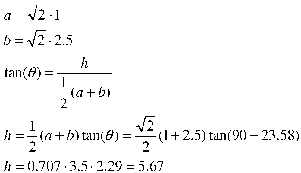
정방형 발광체에 대한 높이:출구 모서리:발광체 모서리 비는 5.67:2.5:1이다. 몇몇 실시예들에서, 이러한 높이를 결정하는데 경험적 방법이 이용될 수 있다. 방사휘도 보전은 최소 출구 면적을 규정하지만 높이는 규정하고 있지 않다.The height: exit edge: emitter edge ratio for the square illuminant is 5.67: 2.5: 1. In some embodiments, an empirical method can be used to determine this height. Radiation preservation prescribes minimum exit area but no height.
다양한 실시예들에 따르면, LED의 발광체층 부분은 위에서 개시된 바와 같이 쉐이핑된다. 보다 구체적으로, 발광체층 물질이 대체로 (상술한 바와 같이 사파이어일 수 있는) 기판과 연속적으로 접촉해 있도록 발광체층은 기판에 대한 제어된 깊이 또는 높이로 쉐이핑된다. 따라서, 몇몇 실시예들에서, 발광물질의 연속층은 기판과 접촉해 있을 수 있다. 몇몇 실시예들에서, 발광체 물질의 연속층은 기판과 전기적 접촉을 이룰 수 있거나 또는 기판의 전기적 평면 또는 연속적인 전기적 접속을 형성할 수 있다. 몇몇 실시예들에서, 발광체층의 일부분만이 쉐이핑된다. 몇몇 실시예들에서, 발광체층은 제어된 깊이 또는 높이로 쉐이핑될 수 있는 쉐이핑된 부분과 쉐이핑되지 않은 부분 또는 구역을 포함할 수 있다.According to various embodiments, the emitter layer portion of the LED is shaped as disclosed above. More specifically, the emitter layer is shaped to a controlled depth or height relative to the substrate such that the emitter layer material is generally in continuous contact with the substrate (which may be sapphire as described above). Thus, in some embodiments, the continuous layer of luminescent material may be in contact with the substrate. In some embodiments, the continuous layer of light emitter material may be in electrical contact with the substrate or may form an electrical plane or continuous electrical connection of the substrate. In some embodiments, only a portion of the emitter layer is shaped. In some embodiments, the emitter layer may include shaped and unshaped portions or regions that can be shaped to a controlled depth or height.
발광체층과 기판 사이의 경계면의 면적은 상술한대로 선택될 수 있으며, 발광체층 물질의 높이는 발광체층의 쉐이핑된 부분내에서 최장거리 또는 대략적으로 최장거리를 횡단하는 하나 이상의 제한 광선들에 기초하여 선택될 수 있다. 특정한 예시로서, 도 2a는 제어된 높이(h)로 쉐이핑된 발광체(20)의 쉐이핑된 부분(10)을 도시한다. 이 예시에서, 쉐이핑된 부분은 발광체층, 예컨대, 비제한적인 예시로서, GaN층 또는 이와 다른 발광체층일 수 있다. 발광체(20)의 발광체층 물질의 쉐이핑되지 않은 부분은 도 2a에서 도시되지 않는다. 일 실시예에서, 상술한 바와 같은 제한 광선은 발광체층의 쉐이핑된 부분에서 최장거리 또는 대략적으로 최장거리를 횡단한다. 따라서, 도 2a의 예시에서, 제한 광선(45)은 발광체층의 쉐이핑된 부분의 깊이 또는 높이(h)에서 대체로 종단되도록 선택될 수 있다.The area of the interface between the light emitter layer and the substrate may be selected as described above, and the height of the light emitter layer material may be selected based on one or more confining rays that traverse the longest or approximately longest distance within the shaped portion of the emitter layer. Can be. As a specific example, FIG. 2A shows the shaped
일 실시예에서, 측벽의 형상은 경험적으로 결정된다. 측벽들에 대해서는 두가지 제약이 존재한다.In one embodiment, the shape of the sidewalls is empirically determined. There are two constraints on the side walls.
a. 발광체로부터 나와서 측벽에 부딪치는 모든 광선들은 임계각 이상의 각도로 이 측벽과 부딪쳐야 한다.a. All light rays coming out of the illuminator and hitting the sidewall must strike the sidewall at an angle above the critical angle.
b. 측벽들로부터 반사되어 나오는 모든 광선들은 출구면을 향해 반사되어야 하며, 출구면에서의 입사각은 임계각 보다 작아야 한다.b. All light rays reflected from the sidewalls should be reflected toward the exit face and the angle of incidence at the exit face should be less than the critical angle.
측벽의 형상에 대한 다른 기준은 출구에서 광 세기의 균일성 또는 무한대의 가우시안 분포, 또는 이 모두, 또는 다른 조건 세트일 수 있다. 따라서, 방출된 빛이 희망하는 세기 또는 각도로 기판에 조사되는 것을 보장하기 위해 측벽들은 쉐이핑될 수 있으며, 이러한 희망하는 세기 또는 각도는 예컨대 기판의 굴절율과 같은 기판의 특성, 발광체 물질 또는 기타의 물질의 특성에 기초하여 결정될 수 있다.Another criterion for the shape of the sidewalls may be the uniformity of the light intensity at the exit or the infinite Gaussian distribution, or both, or another set of conditions. Thus, the sidewalls can be shaped to ensure that the emitted light is irradiated to the substrate at a desired intensity or angle, which desired intensity or angle is characterized by the substrate's properties such as, for example, the refractive index of the substrate, the emitter material or other material. It can be determined based on the characteristics of.
몇몇 실시예들에서, 측벽들의 형상은 반복적으로 결정될 수 있다. 형상은 n개의 면들로 나눠진다. 측벽을 위한 면은 마이크로소프트 엑셀(마이크로소프트 및 엑셀은 워싱톤 레이몬드에 위치한 마이크로소프트사의 상표명들이다)과 같은 컴퓨터 프로그램을 이용하여 정의될 수 있다. 보다 구체적으로, 마이크로소프트 엑셀내의 그래프 특징물이 측벽 형상의 그래프를 생성하기 위해 이용될 수 있다. 동일한 일반적 형상이 각각의 측벽에 사용될 수 있거나 서로 다른 형상들이 서로 다른 측벽들에 사용될 수 있다. 엑셀과 같은 프로그램을 이용하여, 희망하는 성능을 얻도록 각각의 면의 크기 및 각도가 변경될 수 있다. 특정된 측벽 형상을 갖는 (또는 특정된 면에 기초한 곡선형 측벽 형상을 갖는) 쉐이핑된 기판에 대한 입체 모델이 Solidworks, AutoCad, Pro Engineer 등과 같은 임의의 기계적 도안 프로그램을 이용하여 생성될 수 있다. 입체 모델은 또한 Zemax, TracePro, BRO, Lighttools 등과 같은 임의의 광선 추적 프로그램을 이용하여 생성되고 분석될 수 있다.In some embodiments, the shape of the sidewalls can be determined repeatedly. The shape is divided into n faces. The face for the side wall can be defined using a computer program such as Microsoft Excel (Microsoft and Excel are trademarks of Microsoft Corporation, located in Raymond, Washington). More specifically, graph features in Microsoft Excel can be used to generate sidewall shaped graphs. The same general shape may be used for each sidewall or different shapes may be used for different sidewalls. Using a program such as Excel, the size and angle of each face can be changed to achieve the desired performance. A three-dimensional model for a shaped substrate having a specified sidewall shape (or having a curved sidewall shape based on a specified facet) can be generated using any mechanical design program, such as Solidworks, AutoCad, Pro Engineer, and the like. Stereoscopic models can also be created and analyzed using any ray tracing program such as Zemax, TracePro, BRO, Lighttools, and the like.
물리학에서, 광선 추적은 가변적인 전파 속도, 흡수 특성, 및 반사면들의 구역들을 갖는 시스템을 관통하는 파 또는 입자의 경로를 계산하는 방법이다. 이러한 환경들 하에서, 파면은 휘어질 수 있고, 방향을 변경할 수 있거나, 또는 표면들로부터 반사될 수 있어서, 분석을 복잡하게 만든다. 광선 추적은 이산적 양만큼 매질 관통 광선들이라고 불리우는 이상적인 좁은 빔을 반복적으로 진행시킴으로써 이러한 문제점을 해결한다. 단순한 문제들은 단순한 수학식을 이용하여 소수의 광선들을 전파시킴으로써 분석될 수 있다. 보다 상세한 분석들은 수 많은 광선들을 컴퓨터를 이용하여 전파시키도록 함으로써 수행될 수 있다. 전자기 방사의 문제점에 적용될 때에, 빛의 파장보다 훨씬 큰 치수의 물체를 광파들이 관통하여 전파하거나 그 주변을 전파하는 한에서 유효하게 되는 맥스웰 방정식에 대한 근사해(approximate solution)에 광선 추적은 종종 의존한다.In physics, ray tracing is a method of calculating the path of a wave or particle through a system with varying propagation speeds, absorption characteristics, and zones of reflective surfaces. Under these circumstances, the wavefront may bend, change direction, or be reflected from the surfaces, complicating the analysis. Ray tracing solves this problem by repeatedly advancing an ideal narrow beam called medium through rays by discrete amounts. Simple problems can be analyzed by propagating a few rays using simple equations. More detailed analyzes can be performed by allowing a large number of rays to propagate using a computer. When applied to the problem of electromagnetic radiation, ray tracing often relies on an approximate solution to the Maxwell's equation that becomes effective as long as light waves propagate through or propagate an object that is much larger than the wavelength of light. .
상업적으로 이용가능한 광선 추적 프로그램을 이용하여, 광선 추적 및 세기 및 방사휘도 분포 프로파일을 생성하도록 컴퓨터 시뮬레이션이 수행될 수 있다. 만약 결과적인 세기 및 방사휘도 프로파일이 불만족스런 분포를 갖거나 또는 쉐이핑된 기판의 전달 효율이 너무 낮으면, 다양한 면들의 변수들이 조정될 수 있고 시뮬레이션은 다시 수행될 수 있다. 이러한 프로세스는 자동적으로 면 변수들을 조정하는 컴퓨터 프로그램의 이용을 통해 자동화될 수 있다. 설명을 위해, 아래의 예시들은 Zemax 광학 설계 프로그램을 활용한다(Zemax는 워싱톤 벨레뷰에 있는 Zemax Development Corporation의 상표명이다).Using commercially available ray tracing programs, computer simulations may be performed to generate ray tracing and intensity and radiance distribution profiles. If the resulting intensity and radiance profile has an unsatisfactory distribution or the transfer efficiency of the shaped substrate is too low, the parameters of the various faces can be adjusted and the simulation can be performed again. This process can be automated through the use of a computer program that automatically adjusts face variables. For illustrative purposes, the examples below utilize the Zemax optical design program (Zemax is a trademark of Zemax Development Corporation, Bellevue, Washington).
ZemaxZemax 모델 Model
밝기 공식에 의해 명시된 크기 제약 및 제한 광선 고려사항을 충족시키는 형상이 만들어지면, 이 형상은 광선 추적 프로그램내에서 모델링될 수 있다. 광선 추적 프로그램은 광선의 효율성, 근거리장 분포와 원거리장 분포를 결정하는 형상을 광선들이 거치도록 모델링할 것이다.Once a shape is created that meets the size constraints and limiting light considerations specified by the brightness formula, the shape can be modeled in a ray tracing program. The ray tracing program will model the rays through a shape that determines the ray's efficiency, near-field, and far-field distribution.
도 3은 쉐이핑된 측벽들(60, 65)을 갖는 쉐이핑된 부분(10)의 예시적인 입체 모델의 측면도이다. 측벽들(60, 65)을 갖는 쉐이핑된 부분(10)은 정방형 발광체(20)의 발광체층의 쉐이핑된 부분을 나타낸다. 특정한 예시로서, 쉐이핑된 부분(10)은 굴절율이 2.5인 GaN 물질을 대표한다. 출력 분포는 램버시안이다. 3 is a side view of an exemplary three-dimensional model of shaped
도 4는 도 3의 입체 모델속을 진행하는 광선들의 일 예를 도시한다. TIR로 인해, 광선(70)은 측벽들(60, 65)에 반사되어 출구면(55)으로 향하며, 광선들은 출구면(55)에서 굴절되어 이 출구면(55)을 통과한다.4 shows an example of light rays traveling in the three-dimensional model of FIG. 3. Due to the TIR, light rays 70 are reflected on
도 5는 출구 검출기 평면(40)에서 예시적인 정방형 발광체(20)의 방사휘도를 보여주는, Zemax에서 생성된 입체 모델의 스크린샷이다. 임의의 모서리 효과 광선들이 정확하게 기록되는 것을 보장하기 위해 검출기 평면은 출구면(이 경우, 10단위 X 10단위)보다 크게 만들어 진다. 방사휘도는 검출기 평면(40)의 중심부분을 커버한다. GaN 물질의 경우, 도 5는 GaN 출구에서의 근거리장 분포를 도시한다.5 is a screenshot of a stereoscopic model generated at Zemax, showing the radiance of an exemplary
도 6은 검출기 평면(40)에서의 방사 세기를 보여주는, 도 5의 입체 모델의 다른 스크린샷이다. 출구면에서의 방사 세기는 원거리에서의 방사휘도와 동등하며 이것은 종종 원거리장 분포라고 불리어진다. GaN 물질의 경우, 도 6은 GaN 뒤의 원거리장 분포를 나타낸다.6 is another screenshot of the three-dimensional model of FIG. 5 showing the radiation intensity in the
도 5와 도 6은 빛을 대기 밖으로 내보낼 때의 쉐이핑된 LED의 실시예의 효율성을 예시화한 것이다. 이 경우, 방출된 빛의 대략 94%가 발광체층으로부터 추출된다. 이것은 여러 물질층들내의 흡수 손실 및 프레넬 손실을 고려하고 있지 않다. 사파이어에서의 흡수 손실은 무시가능하며, GaN층은 매우 얇다. 몇몇 실시예들에서, GaN층은 대략 4-5 미크론의 두께를 가질 수 있다. 프레넬 손실은 다음과 같다:5 and 6 illustrate the efficiency of embodiments of shaped LEDs when emitting light out of the atmosphere. In this case, approximately 94% of the emitted light is extracted from the emitter layer. This does not account for absorption loss and Fresnel loss in the various material layers. Absorption losses in sapphire are negligible, and the GaN layer is very thin. In some embodiments, the GaN layer may have a thickness of approximately 4-5 microns. Fresnel loss is as follows:
[수학식 5][Equation 5]

프레넬 손실이 고려될 때에 발광체층으로부터 추출된 빛은 대략 84%이다.When Fresnel loss is considered, the light extracted from the emitter layer is approximately 84%.
기판의 출구면에 무반사 코팅을 추가함으로써, 사파이어 대 공기 프레넬 손실은 제거될 수 있다. 그러면 총 효율은 다음과 같을 것이다:By adding an antireflective coating to the exit face of the substrate, sapphire to air fresnel loss can be eliminated. The total efficiency would then be:
[수학식 6]&Quot; (6) "
![]()
![]()
HEXHEX 기하구조 Geometry
정방형 발광체는 공간을 낭비하는 것 없이 서로가 완벽하게 끼워 맞춰진다는 장점을 갖는다. 또한, 다이싱 동작은 두 개의 직교하는 절단만을 갖도록 단순화된다. 정방형 발광체에 관한 추가적인 가르침을 얻고자 한다면, 독자들은 "LED SYSTEM AND METHOD"이라는 명칭으로 2007년 10월 1일에 출원된 미국 특허 출원 제11/906,219 호 및 제11/906,194호를 참조바란다. 정방형 프로파일은 동일한 길이의 변들을 갖는 직사각형 프로파일이라는 것을 유념해야 한다. 아래의 예시적인 실시예들에서는 육각형 발광체들이 설명되지만, 본 발명분야의 당업자는 본 명세서에서 개시된 방법들이 다양한 형상들에 적용될 수 있으며, 임의의 특정한 형상, 크기, 구성 또는 물질로 제한되지 않는다는 것을 알 것이다.Square light emitters have the advantage that they fit perfectly together without wasting space. In addition, the dicing operation is simplified to have only two orthogonal cuts. For further teaching on square light emitters, readers are referred to US patent applications Ser. Nos. 11 / 906,219 and 11 / 906,194, filed Oct. 1, 2007, entitled " LED SYSTEM AND METHOD. &Quot; It should be noted that the square profile is a rectangular profile with sides of the same length. Although hexagonal emitters are described in the following exemplary embodiments, one of ordinary skill in the art appreciates that the methods disclosed herein can be applied to various shapes and are not limited to any particular shape, size, configuration or material. will be.
육각 패턴은 어떠한 공간도 낭비하는 것 없이 서로가 끼워 맞춰질 수 있다. 쉐이핑된 디바이스에서, 육각 패턴은 정방형 디바이스보다 낮은 물질 부피를 제공해줄 수 있다. 도 7a 내지 도 7d는 육각형 발광체(720)의 일 실시예의 도식도의 다양한 모습들을 도시한다.Hexagonal patterns can fit together without wasting any space. In the shaped device, the hexagonal pattern can provide a lower material volume than the square device. 7A-7D show various views of a schematic diagram of one embodiment of
면적비는 밝기 공식에 의해 명시되며, 이에 따라 발광체 면적(750) 대비 출구 면적(755) 비는 6.25:1 비율을 유지한다. 하지만, 높이(h)는 다음과 같이 감소될 것이다:The area ratio is specified by the brightness formula, whereby the ratio of the
[수학식 7][Equation 7]

이제 높이는 위의 [수학식 4]에서 서술된 정방형 발광체(20)의 경우였을 때의 5.67 대신 4.01이다. 이 예시에서의 높이:한쪽끝 모서리:발광체 모서리 비는 4.01:2.5:1이다.The height is now 4.01 instead of 5.67 when in the case of the square light-emitting
이러한 기초 단위 치수를 이용하여, 입체 모델이 생성되고 모델링될 수 있다. 예를 들어, 입체 모델은 ProE에서 생성될 수 있고, 그런 다음 Zemax에서 모델링될 수 있다. 도 8은 발광체층(80)을 쉐이핑함으로써 생성된 육각형 발광체(820)의 일 실시예의 도식도이다. 이 예시에서, 발광체층(80)은 쉐이핑된 부분(81)과 쉐이핑되지 않은 부분(82)을 포함한다. 쉐이핑된 부분(81)에서, 기판(810)과 측벽들(860, 865)은 광 추출 효율을 최대화시키기 위해 상술한 바와 같이 제어된 높이 h로 쉐이핑되고, 이로써 경계면(850)을 통과하여 기판(810)에 진입하는 양자 우물 구역(815)으로부터의 광자들이 최소한의 에너지 손실을 갖고 출구면(855)을 빠져 나갈 수 있도록 해준다. 양자 우물 구역에 관한 추가적인 가르침을 얻고자 한다면, 독자들은 "LED SYSTEM AND METHOD"이라는 명칭으로 2007년 10월 1일에 출원된 미국 특허 출원 제11/906,219호 및 제11/906,194호를 참조바란다.Using this elementary unit dimension, a three-dimensional model can be generated and modeled. For example, a stereoscopic model can be generated in ProE and then modeled in Zemax. 8 is a schematic diagram of one embodiment of a
도 9는 발광체층(80)을 포함하는, 복수의 층들(920)을 갖는 LED(900)의 일 실시예의 도식도이다. 발광체층(80)으로부터 방출된 빛은 경계면(101)을 통해 기판(90)에 진입하고, 기판(90)을 나와서 경계면(102)을 거쳐 대기로 나간다. 일 실시예에서, 기판(90)은 사파이어이다. 육각형 발광체(820)의 효율은 Zemax에서 분석된 입체 모델에 따라 대략 95.5%이다. 즉, 방출된 빛의 대략 95.5%가 발광체층으로부터 추출된다. 프레넬 손실을 고려하면, 총 추출 효율은 대략 85%이다:9 is a schematic diagram of one embodiment of an
[수학식 8][Equation 8]

도 10은 출구 검출기 평면에서의 근거리장 분포를 도시하는, 육각형 발광체의 입체 모델의 스크린샷이다. 도 11은 출구 검출기 평면 뒤의 원거리장 분포를 도시하는, 도 10의 입체 모델의 다른 스크린샷이다. 정방형으로 쉐이핑된 디바이스의 경우에서와 같이, 프레넬 손실을 제거시키기 위해 무반사 코팅이 사파이어 대 공기 경계면[경계면(102)]에서 추가될 수 있다. 그러면 총 추출 효율은 대략 92.6%가 될 것이다.10 is a screenshot of a three-dimensional model of a hexagonal illuminant showing near field distribution in the exit detector plane. 11 is another screenshot of the three-dimensional model of FIG. 10 showing the far field distribution behind the exit detector plane. As in the case of square shaped devices, an antireflective coating can be added at the sapphire to air interface (boundary 102) to eliminate Fresnel loss. The total extraction efficiency will then be approximately 92.6%.
마이크로 발광체들의 어레이Array of micro light emitters
GaN 쉐이핑의 한가지 장점은 하나의 LED를 생성하기 위한 대규모의 발광체들의 어레이를 쉐이핑하는 능력이다. 다른 장점은 미소 발광체들을 통해, 제거된 총체적인 부피가 또한 감소된다는 것이다. 도 12는 기판(90), 발광체층(80), 및 N접촉층(60)을 포함하는 LED(120)의 일 실시예의 도식도이다. 일 실시예에서, 기판(90)은 사파이어이다. 일 실시예에서, N접촉층(60)은 하나 이상의 N접촉점들을 포함한다. 일 실시예들에서, 발광체층(80)은 육각형으로 쉐이핑된 마이크로 LED들의 어레이를 포함한다. 일 실시예들에서, 발광체층(80)은 육각형으로 쉐이핑된 마이크로 LED들의 M x M 어레이를 포함한다. 일 실시예에서, LED(120)는 대략 100 미크론(W) x 100 미크론(L) x 80 미크론(D)이다. 도 12의 예시에서, 육각형으로 쉐이핑된 마이크로 LED들의 어레이는 발광체층(80)을 쉐이핑함으로써 형성된다. 개시된 시스템 및 방법의 실시예들은 임의의 기판을 활용하여도 여전히 방출된 광자들 모두 또는 대체로 모든 광자들을 추출해낼 수 있다. 이 예시를 위해, 기저 기판은 사파이어이지만, 다른 기판들이 사용될 수 있다.One advantage of GaN shaping is the ability to shape large arrays of emitters to produce one LED. Another advantage is that through the microluminaries, the total volume removed is also reduced. 12 is a schematic diagram of one embodiment of an
상술한 바와 같이, 발광체층의 쉐이핑된 부분은 기판과 대체로 연속적인 접촉을 이루고 전기적 평면을 형성하거나 또는 대체로 연속적인 전기적 접속부를 형성하는 쉐이핑되지 않은 부분에 대한 통로를 가져다준다. N접촉부는 전기적 평면을 형성하는 발광체층의 쉐이핑되지 않은 부분과 전기적 접속을 이룸으로써 전류가 발광체층의 쉐이핑되지 않은 부분을 거쳐서 발광체층의 쉐이핑된 부분으로 흐를 수 있도록 해준다. 일 실시예에서, N접촉부는 기판의 쉐이핑된 부분과 쉐이핑되지 않은 부분을 전원에 전기적으로 결합시켜줄 수 있는 금속 합금과 같은 전류 전도성 물질일 수 있다.As noted above, the shaped portion of the emitter layer provides a passage for the unshaped portion that is in general continuous contact with the substrate and forms an electrical plane or that generally forms a continuous electrical connection. The N contact portion makes an electrical connection with the unshape portion of the light emitting layer forming the electrical plane so that current can flow through the unshape portion of the light emitting layer to the shaped portion of the light emitting layer. In one embodiment, the N contact portion may be a current conducting material such as a metal alloy that can electrically couple the shaped and unshaped portions of the substrate to the power source.
대안적인 실시예에서, 발광체층의 쉐이핑되지 않은 부분은 모서리들에서 전원에 결합될 수 있거나 또는 하나 이상의 쉐이핑된 부분들이 전원에 결합될 수 있거나, 또는 상기 구성의 임의의 조합 또는 다른 전류 공급 방법 또는 시스템이 이용될 수 있다. N접촉부보다 작고, N접촉부보다 개수가 많은 P접촉부가 또한 전원에 결합될 수 있다.In an alternative embodiment, the unshaped portion of the emitter layer may be coupled to the power source at the corners or one or more shaped portions may be coupled to the power source, or any combination of the above configurations or other current supply methods or The system can be used. P contacts smaller than the N contacts and larger in number than the N contacts may also be coupled to the power source.
상술한 구성은 마운팅, 열 방산 및 조명의 균일성에서 추가적인 장점들을 갖는다. 매우 작은 크기의 각각의 마이크로 LED와 결합된 각각의 마이크로 LED의 탈출각은 빛이 기판의 두께내에서 여전히 감금된 동안에 하나의 디바이스로부터의 출구 광선들이 이웃하는 많은 수의 마이크로 LED들의 출구 광선들과 중첩되도록 해줄 것이다. 빛이 기판의 출구면에 도달할 때, 수 많은 마이크로 LED들로부터의 빛은 평균화되어서 매우 균일한 광 출력 프로파일을 생성시킨다. 몇몇 실시예들에 따르면, 발광체층내의 마이크로 LED들의 개수는 하나에서 소수 개까지, 또는 수천개까지, 또는 수백만개 또는 그 이상까지의 범위에서 존재할 수 있다.The above arrangement has additional advantages in mounting, heat dissipation and uniformity of illumination. The exit angle of each micro LED combined with each micro LED of very small size is determined by the exit rays of a large number of micro LEDs where the exit rays from one device neighbor while the light is still confined within the thickness of the substrate. Will allow them to overlap. When light reaches the exit face of the substrate, the light from the many micro LEDs is averaged to produce a very uniform light output profile. According to some embodiments, the number of micro LEDs in the emitter layer may be in the range of one to a few, or thousands, or millions or more.
열적 관점으로부터, 각각의 마이크로 LED의 발광 베이스는 마이크로 LED에 전력을 제공해주며 또한 마이크로 LED에 대한 열 제거 통로를 제공해주는 서브마운트에 직접 접합될 수 있다. 이것은 본질적으로 우수한 열 발산을 제공해준다. 발광체들은 서로 멀리 흩어져있기 때문에, 열적 밀도가 또한 감소될 수 있다.From a thermal point of view, the light emitting base of each micro LED can be directly bonded to a submount that provides power to the micro LED and also provides a heat removal path to the micro LED. This inherently provides good heat dissipation. Since the luminous bodies are scattered far from each other, the thermal density can also be reduced.
마찬가지로, P층에 대한 전력은 LED의 표면에 모두 걸쳐서 매우 많은 갯수의 작은 점들로 제공되며, 이에 따라 전력은 서브마운트상의 거의 연속적인 금속화 평면에 의해 이러한 점들에 인가될 수 있다. 이것은 우수한 전류 확산을 제공해준다. 전류 확산은 디바이스로부터의 광출력의 최대량을 제공할 시에 알려진 문제점이다. 개선된 전류 확산을 달성하기 위해 본 발명분야에서는 P형 및 N형 GaN의 여러 레이아웃들에 관한 많은 구성들이 이용된다. 마이크로 LED 구성은 본질적으로 이러한 확산을 제공해준다.Similarly, power to the P layer is provided at a very large number of small points all over the surface of the LED, so that power can be applied to these points by a nearly continuous metallization plane on the submount. This provides good current spreading. Current spreading is a known problem when providing the maximum amount of light output from a device. Many configurations for the various layouts of P-type and N-type GaN are used in the present invention to achieve improved current spreading. Micro LED configurations inherently provide this diffusion.
보다 구체적으로, N층에서의 전류 확산은 N층내로의 비교적 소수의 접촉점들에 의해 달성되는데, 이것은 N층의 두께가 P층의 두께에 비해 크기때문이다. 예를 들어, 도 12에서 도시된 네 개의 위치들에서 N층에 접촉하는 것이 이것을 달성하는 한가지 방법이다. 이와 달리, N층은 중심점에서 접촉될 수 있거나 또는 어레이의 가장자리 주변의 다수의 점들에서 접촉될 수 있다.More specifically, current spreading in the N layer is achieved by a relatively few contact points into the N layer, because the thickness of the N layer is large compared to the thickness of the P layer. For example, contacting the N layer at the four locations shown in FIG. 12 is one way to accomplish this. Alternatively, the N layer can be contacted at the center point or at multiple points around the edge of the array.
제조 방법Manufacturing method
에칭etching
에칭은 적절한 형상을 만들기 위해 고도로 제어된 방법으로 기판 물질을 제거하는 화학적 프로세스를 말한다. 일반적으로 두가지 유형의 에칭 방법들, 즉 습식 에칭과 건식 에칭이 존재한다: 습식 에칭은 기판 물질을 제거하기 위해 액상 에천트를 이용하는 것을 수반한다. 건식 에칭, 플라즈마 에칭 및 반응 이온 에칭에서, 이온들이 생성되어 기판상에 제공된다. 화학적 반응에 기초하거나 또는 입자 모멘텀에 기초하던지 간에, 물질이 기판으로부터 제거된다.Etching refers to a chemical process that removes substrate material in a highly controlled manner to produce the proper shape. There are generally two types of etching methods, wet etching and dry etching: wet etching involves using a liquid etchant to remove the substrate material. In dry etching, plasma etching and reactive ion etching, ions are generated and provided on a substrate. Whether based on chemical reactions or particle momentum, the material is removed from the substrate.
(양자 우물 구역을 포함하는 물질을 더 포함할 수 있는) 기판 물질의 웨이퍼로 시작하여, 포토레지스트의 특정한 패턴이 웨이퍼의 일면상에 증착될 수 있다. 그런 후 웨이퍼는 에칭된다. 포토레지스트로 뒤덮힌 웨이퍼상의 위치들은 에칭되지 않을 것인 반면에, 포토레지스트가 없는 장소에서는 물질이 제거될 것이다. 포토레지스트의 가장자리에서 희망하는 외형을 달성하기 위해 이러한 프로세스를 조정하는 방법은 많이 있다. 예를 들어, 포토레지스트의 두꺼운 층들은 도포되어 후에 에칭 프로세스 동안에 희생적으로 제거되거나, 또는 기타의 희생층들이 포토레지스트와 결합하여 이용될 수 있다. 이러한 층들은 LED기판의 희망하는 외형을 생성하기 위한 이와 같은 방법으로 에천트에 의해 시간이 지나면서 제거된다. 이것은 쉐이핑된 기판들을 생성하기 위해 웨이퍼를 정확하게 에칭하는데 활용될 수 있다. 다른 방법은 다수의 레지스트들과 다수의 에칭 단계들을 이용하는 것이다. 각각의 포토레지스트와 각각의 단계는 작은 물질층을 제거하는데 이용될 수 있다. 다수의 작은 단계들은 희망하는 3D 형상을 얻는데 이용될 수 있다.Starting with a wafer of substrate material (which may further include a material including quantum well zones), a particular pattern of photoresist may be deposited on one side of the wafer. The wafer is then etched. The locations on the wafer covered with the photoresist will not be etched while the material will be removed in the absence of the photoresist. There are many ways to tailor this process to achieve the desired appearance at the edge of the photoresist. For example, thick layers of photoresist may be applied and later sacrificially removed during the etching process, or other sacrificial layers may be used in combination with the photoresist. These layers are removed over time by the etchant in such a way to create the desired appearance of the LED substrate. This can be utilized to accurately etch the wafer to produce shaped substrates. Another method is to use multiple resists and multiple etching steps. Each photoresist and each step can be used to remove small layers of material. Many small steps can be used to obtain the desired 3D shape.
에칭 파라미터는 기판 물질에 기초할 수 있다. 에칭율은 에천트와 기판에 따라 달라진다. 사파이어와 실리콘 카바이드와 같은 LED 응용들에서 이용되는 기판 물질들의 경우, 반응 이온 에칭을 이용한 에칭율은 분 당 250nm 내지 2.5μm의 범위에 이를 수 있는데, 이것은 상업적 제조목적상 느려질 수 있다. 실리콘 카바이드는 위 에칭율의 상한쪽에 있는 반면에 사파이어는 하한쪽에 있다.Etching parameters may be based on the substrate material. Etch rates vary with etchant and substrate. For substrate materials used in LED applications such as sapphire and silicon carbide, the etch rate using reactive ion etching can range from 250 nm to 2.5 μm per minute, which can be slow for commercial manufacturing purposes. Silicon carbide is at the upper end of the upper etch rate, while sapphire is at the lower end.
몇몇 실시예들에서, InGaN/GaN계 에피(epi) 구조의 GaN 측벽들의 쉐이핑은 원환형 렌즈 템플릿을 이용하여 Cl2/BCl3/Ar 플라즈마에서 다단계 건조 에칭 프로세스에 의해 수행될 수 있다. 몇몇 실시예들에서, n-GaN 및 n-GaN 및 InGaN 층들의 이러한 건조 에칭 프로세스는 포토레지스트와 Ni 포토 마스트를 이용하여 유도 결합된 플라즈마 반응 이온 에칭(inductively coupled plasmas reactive ion etching; ICP-RIE)에 의해 수행될 수 있다. 일정한 ICP/바이어스 전력, 즉 300/100 W 및 4 mTorr 체임버 압력에서 0.5nm 미만의 낮은 에칭면 거칠기를 유지하기 위해 Cl2/BCl3/Ar의 제어된 기체 흐름율이 이용될 수 있다. n-GaN을 위한 12,000 Å/min의 에칭율은 낮은 흐름율(Cl2/BCl3/Ar) 기체 혼합물을 이용하여 30 mTorr, 300 W ICP, 100 W 바이어스 전력에서 예상된다. 다단계 에칭 프로세스 동안에 GaN 측벽들의 낮은 표면 거칠기를 유지하기 위해 케어(Care)가 이용되어야 한다. 예로서, 100 W의 바이어스 전력에서 1nm 미만의 낮은 RMS(root mean square) 거칠기값이 유지되어야 한다.In some embodiments, shaping of GaN sidewalls of an InGaN / GaN based epi structure may be performed by a multi-step dry etching process in a Cl 2 / BCl 3 / Ar plasma using an annular lens template. In some embodiments, this dry etching process of n-GaN and n-GaN and InGaN layers is inductively coupled plasmas reactive ion etching (ICP-RIE) using photoresist and Ni photomasks. It can be performed by. A controlled gas flow rate of Cl 2 / BCl 3 / Ar can be used to maintain a low etch surface roughness of less than 0.5 nm at a constant ICP / bias power, ie 300/100 W and 4 mTorr chamber pressure. An etch rate of 12,000 mW / min for n-GaN is expected at 30 mTorr, 300 W ICP, 100 W bias power using a low flow rate (Cl 2 / BCl 3 / Ar) gas mixture. Care should be used to maintain low surface roughness of GaN sidewalls during the multi-step etch process. As an example, a low root mean square (RMS) roughness value of less than 1 nm should be maintained at a bias power of 100 W.
GaN의 평탄한 거울형태의 면을 달성하기 위해 InGaN/GaN계 구조의 테이퍼 벽의 에칭의 경우, 비교적 높은 Cl2 흐름율과 낮은 체임버 압력(~ 4 mTorr)이 지속되어야 한다. ICP 전력 및 체임버 압력 최적화는 주의해서 수행되어야 하는데, 그 이유는 에칭된 면들의 테이퍼 형상은 항상 각자의 선택된 파라미터들에 의존하기 때문이다. 본 발명분야의 당업자에 의해 이해되는 바와 같이, 적절한 에칭 파라미터를 이용하여, InGaN/GaN계 발광 다이오드의 제조에 이용될 수 있는 n-GaN 의 거울형태의 측벽면들이 획득될 수 있다. 더군다나, 고정된 기체 흐름율, 및 비교적 낮은 ICP/바이어스 전력 및 체임버 압력에서, InGaN계 물질 테이퍼 측벽들 형상은 한층 더 개선되고 수정될 수 있다.In order to achieve a flat mirrored surface of GaN, the etching of the tapered wall of the InGaN / GaN-based structure requires a relatively high Cl 2 flow rate and low chamber pressure (-4 mTorr) to be maintained. ICP power and chamber pressure optimization must be done with caution because the taper shape of the etched faces always depends on the respective selected parameters. As will be appreciated by those skilled in the art, using appropriate etching parameters, n-GaN mirrored sidewall surfaces can be obtained that can be used to fabricate InGaN / GaN based light emitting diodes. Furthermore, at a fixed gas flow rate, and relatively low ICP / bias power and chamber pressure, the InGaN-based material taper sidewall shapes can be further improved and modified.
도 13은 발광체층(80)의 쉐이핑된 부분(81)에서 형성된 육각형 발광체들(820)의 어레이를 갖는 발광체층(80)과 기판(90)을 포함하는 LED(130)의 일 실시예의 도식도이다. 도 13에서 도시된 바와 같이, 발광체층의 일부분 또는 발광체층 일부층은 위의 도 8에서 도시된 쉐이핑된 측벽들을 가질 수 있는 마이크로 LED 발광체들의 어레이를 형성하도록 발광체층 물질을 제거함으로써 쉐이핑된다. 보다 구체적으로, 발광체들(820)간에 각각의 에칭 채널들(131)을 남겨두고 발광체층 물질(80)의 일반적으로 연속적인 쉐이핑되지 않은 층(82)이 기판(90)에 접하도록 하면서, 발광체층(80)은 기판(90)에 대한 제어된 높이 또는 깊이로 쉐이핑된다. 일 실시예에서, 각각의 에칭 채널(131)은 대략 0.4 미크론 폭을 갖는다. 즉, 이 예시에서, 마이크로 LED들(820)은 가장 좁은 지점에서 대략 0.4 미크론 만큼 이격될 수 있다.FIG. 13 is a schematic diagram of one embodiment of an
도 13에서, 기판(90)에 접하는 발광체층(80)의 쉐이핑되지 않은 부분(82)은 쉐이핑되지 않은 발광체층 물질이 일반적으로 기판과 연속적인 접촉을 이루는 연속적인 N-GaN층(132)을 형성한다. 따라서, 일 실시예에서, 기판과 대체로 접촉해 있는 발광체층 물질의 연속층이 존재할 수 있으며, 이것은 전기적 접촉을 이루거나 또는 전기적 평면 또는 연속적인 전기적 접속부를 형성할 수 있다. 하나 이상의 실시예들에서, 발광체층 물질의 모든 부분 또는 대체로 모든 부분이 쉐이핑되지는 않기 때문에, 측벽을 형성하기 위해 제어된 깊이 또는 높이로 쉐이핑될 수 있는 발광체층의 쉐이핑된 부분과 쉐이핑되지 않은 (발광체층 물질의) 발광체층의 쉐이핑되지 않은 부분 또는 구역이 존재할 것이다. 일 실시예에서, 상술한 바와 같은 제한 광선은 발광체층의 쉐이핑된 부분에서 최장거리 또는 대략적으로 최장거리를 횡단한다(즉, 제한 광선은 쉐이핑된 마이크로 LED 발광체를 횡단할 수 있다). 따라서, 기판에 대한 발광체층의 쉐이핑된 부분의 깊이 또는 높이로 대체로 종단되도록 제한 광선이 선택될 수 있다. 추가로 상술한 바와 같이, 발광체층 물질(예컨대, 마이크로 LED 발광체들의 측벽들)은 발광체층의 쉐이핑된 부분에서 최장거리 또는 대체적으로 최장거리를 횡단하는 하나 이상의 제한 광선들에 기초하여 쉐이핑될 수 있다.In FIG. 13, the
다단계 메사 에칭 프로세스Multistage Mesa Etching Process
도 14는 다단계 메사 에칭 프로세스의 일 실시예의 도식도이다. 본 발명개시내에서, “메사”란 에칭 이후에 남아서 “메사”로서 나타나는 것을 형성하고 디바이스의 발광 부분이 되는 웨이퍼의 섹션을 말한다. 단계 141에서, 발광체층(80)은 에칭 채널(131)의 바닥을 정의하도록 패턴화된다. 단계 142에서, 등방성 에칭 화학물이 직선형 또는 거의 직선형의 측벽들을 달성하는데 이용된다. 단계 143에서, 발광체층(80)은 에칭 채널(131)의 상단부를 정의하도록 다시 패턴화된다. 단계 144에서, 이방성 에칭 화학물이 측벽상의 만곡부를 생성하는데 이용된다. 몇몇 실시예들에서, 후속하는 프로세싱은 금속화 및 패시베이션을 포함할 수 있다. 다양한 실시예들에서, 발광체층들의 최종적인 프로파일을 보다 잘 정제시키는데에 다수의 포토 및 에칭 단계들이 이용될 수 있다. 측벽 프로파일을 직선형(등방성)에서 곡선형(이방성)으로 변경시키는데에 에칭 화학작용이 선택될 수 있다. 이것은 곡선형 형상을 생성하기 위해 단일 단계를 통해 행해질 수 있거나, 또는 다양한 면들을 발광체층 측벽 형상에서 에칭하기 위해 다단계로 행해질 수 있다. 제조 단계의 순서는 희망하는 바에 따라 달라질 수 있다. 예를 들어, 메사의 상단이 제일 먼저 정의되고 이어서 포토 에칭이 뒤따를 수 있다. 단계들은 epi 구조물내에서 보다 깊이 에칭할 수 있다.14 is a schematic of one embodiment of a multi-step mesa etch process. Within the present disclosure, “mesa” refers to a section of a wafer that remains after etching to form what appears as “mesa” and becomes the light emitting portion of the device. In step 141, the
도 14의 예시에서, LED(140)의 일 실시예는 상술한 다단계 메사 에칭 프로세스에 의해 제조될 수 있다. 이 예시에서, LED(140)는 기판(90)과 발광체층(80)을 포함한다. 이 예시에서, 발광체층(80)은 기판(90)에 접해있는 발광체층(80)의 쉐이핑되지 않은 부분(82)을 남겨두고, 상술한 다단계 메사 에칭 프로세스에 의해 형성된 쉐이핑된 부분(81)을 포함한다. 다단계 메사 에칭 프로세스의 패턴화 및 에칭 단계들은 발광체들(820)간에 에칭 채널들(131)을 생성한다. 도 8을 참조하여 상술한 바와 같이, 각각의 발광체(820)는 쉐이핑된 측벽들(860)을 갖는 쉐이핑된 기판(810)과 양자 우물 구역(815)을 포함할 수 있다. 쉐이핑된 기판(810)은 발광 물질로 이루어진다. 일 실시예에서, 발광물질은 GaN이다. 일 실시예에서, 기판(90)은 사파이어이다. In the example of FIG. 14, one embodiment of LED 140 may be fabricated by the multi-step mesa etching process described above. In this example, the LED 140 includes a
다른 에칭 프로세스가 또한 LED(140)를 생산하는데 이용될 수 있다. 예를 들어, 발광체층을 쉐이핑하기 위한 하나의 방법 실시예는, 다음과 같은 순서로, 기판상에 p층 금속을 증착시키는 단계, p층 금속상에 반사층을 증착시키는 단계, 반사층상에 SiO2 보호층(버퍼)를 증착시키는 단계, 증착층들을 희망하는 형상으로 에칭하는 단계, 및 이어서 n층 금속을 증착시키는 단계를 포함할 수 있다. 다른 예로서, 발광체층을 쉐이핑하기 위한 하나의 방법 실시예는, 다음과 같은 순서로, 마스크 A 패턴을 증착시키는 단계, 마스크 A 패턴에 따라 원하지 않는 물질을 에칭하여 제거하는 단계, 마스크 B 패턴을 증착시키는 단계, 마스크 B 패턴에 따라 추가적인 물질을 에칭하여 제거하는 단계, 희망하는 높이를 구축시키기 위해 패턴화-에칭 단계들을 반복하는 단계, n층 금속을 증착시키는 단계, n층 금속의 상부상에 p층 금속을 증착시키는 단계, 및 최종적으로 반사층을 증착시키는 단계를 포함할 수 있다.Other etching processes may also be used to produce the LEDs 140. For example, one method embodiment for shaping a luminescent layer may include depositing a p layer metal on a substrate, depositing a reflective layer on the p layer metal, SiO 2 on the reflective layer in the following order: Depositing a protective layer (buffer), etching the deposited layers into a desired shape, and then depositing an n-layer metal. As another example, one method embodiment for shaping an illuminant layer may include depositing a mask A pattern, etching and removing unwanted materials in accordance with the mask A pattern, and removing the mask B pattern in the following order: Depositing, etching and removing additional material according to the mask B pattern, repeating patterning-etching steps to build the desired height, depositing n-layer metal, on top of the n-layer metal depositing the p-layer metal, and finally depositing the reflective layer.
몇몇 실시예들은 직선형 측벽을 얻어내기 위한 등방성 에칭 단계를 생략하고, 일 실시예에서 GaN을 포함하는 발광물질을 쉐이핑하는 단계로 바로 이동할 수 있다. 예를 들어, 발광체층을 쉐이핑하기 위한 하나의 방법 실시예는, 다음과 같은 순서로, p층 금속으로 기판을 블랭킷 코팅하는 단계, p층 금속으로 코팅된 기판을 포토레지스트 패턴화하는 단계, 및 이에 따라 희망하지 않는 물질을 에칭하여 제거하는 단계를 포함할 수 있다. 일 실시예에서, ICP-RIE가 발광체층으로부터 희망하지 않는 물질을 에칭하여 제거하는데 활용된다. 다른 에칭 방법이 또한 사용될 수 있다.Some embodiments may skip the isotropic etching step to obtain straight sidewalls, and may move directly to shaping the light emitting material including GaN in one embodiment. For example, one method embodiment for shaping a light emitter layer includes blanket coating a substrate with a p layer metal, photoresist patterning a substrate coated with a p layer metal, in the following order: This may include etching away the unwanted material. In one embodiment, ICP-RIE is utilized to etch away unwanted material from the emitter layer. Other etching methods can also be used.
이 방법은 단하나의 마스크 GaN 프로파일을 이용하며, 이에 따라 생성된 p접촉부는 하드 마스크로서 이용되고, 이로써 메사에 되정렬할 필요를 없애주며 포토레지스트 패턴화 단계를 제거시켜준다. 염소(Cl2) 기체와 삼염화붕소(BCl3) 기체의 농도를 변화시킴으로써, 상이한 GaN 에칭 기울기가 얻어질 수 있다. 보다 구체적으로, 몇몇 실시예들에서, GaN 물질이 에칭될 때에, Cl2 와 BCl3 농도들의 비율을 변경시켜서 국부적 기울기에 영향을 미치도록 하는 일련의 단계들이 수행된다. 예컨대, 보다 큰 농도의 Cl2 또는 Cl2만을 이용하여 보다 직선적인 측벽이 획득될 수 있다. BCl3-다량함유된 화학물은 측벽을 패시베이팅하기 위한 폴리머를 생성한다. 높이 = 0에서 특정한 기울기를 얻기 위해, Cl2와 BCl3 플라즈마는 특별한 농도비율을 가질 수 있다. 높이 = 1에서 다른 기울기를 얻기 위해, Cl2와 BCl3의 농도비율은 달라질 수 있다. 위 단계들은 희망하는 높이에 도달될 때 까지 반복될 수 있다. 발광체층의 높이 전부에 걸쳐서 그리고 에칭 플라즈마의 농도비율에 따라, 발광체층내의 각각의 마이크로 LED의 측벽들의 기울기는 매우 완만한 것에서부터 매우 급경사진 것으로 변할 수 있으며, 이에 따라 발광체층을 쉐이핑할 수 있다. This method uses a single mask GaN profile, and the resulting p-contacts are used as hard masks, thereby eliminating the need for realignment to the mesa and eliminating the photoresist patterning step. By changing the concentrations of chlorine (Cl 2 ) gas and boron trichloride (BCl 3 ) gas, different GaN etch slopes can be obtained. More specifically, in some embodiments, when the GaN material is etched, a series of steps are performed to alter the ratio of Cl 2 and BCl 3 concentrations to affect the local slope. For example, more linear sidewalls can be obtained using only higher concentrations of Cl 2 or Cl 2 . BCl 3 -rich chemicals produce polymers for passivating sidewalls. To obtain a specific slope at height = 0, the Cl 2 and BCl 3 plasmas can have a special concentration ratio. To obtain different slopes at height = 1, the concentration ratios of Cl 2 and BCl 3 can vary. The above steps can be repeated until the desired height is reached. Over the height of the emitter layer and depending on the concentration ratio of the etch plasma, the slope of the sidewalls of each micro LED in the emitter layer can vary from very gentle to very steep, thus shaping the emitter layer. .
몇몇 실시예들은 프로파일링된 GaN 에칭을 위해 두 개의 마스크 물질로 단일 포토레지스트 패턴을 활용할 수 있다. 예를 들어, 발광체층을 쉐이핑하기 위한 하나의 방법 실시예는 다음의 특징들을 포함할 수 있다:Some embodiments may utilize a single photoresist pattern with two mask materials for profiled GaN etching. For example, one method embodiment for shaping the illuminant layer may include the following features:
1) 포토레지스트 패턴은 최종적인 GaN 면적에 비해 큰 크기를 갖는다.1) The photoresist pattern has a large size compared to the final GaN area.
2) 추가적인 프로파일 제어를 위해 포커스/노출이 측벽들을 경사지게 하는데 활용될 수 있다.2) Focus / exposure can be utilized to tilt the sidewalls for additional profile control.
3) 하드 마스크용으로 산화물을 이용한다. 일 실시예에서, BOE/HF에서 하드 마스크가 에칭될 수 있거나 또는 육플루오르화황(SF6) 플라즈마 에칭된다. BOE(Buffered Oxide Etch)는 보다 제어된 실리콘 산화물의 에칭율을 갖는 플루오르화 암모늄과 플루오린화 수소산(HF)의 혼합물이다.3) Oxide is used for the hard mask. In one embodiment, the hard mask may be etched in BOE / HF or sulfur hexafluoride (SF 6 ) plasma etch. Buffered Oxide Etch (BOE) is a mixture of ammonium fluoride and hydrofluoric acid (HF) with a more controlled etching rate of silicon oxide.
4) 대략 1:1의 레지스트 에칭율과 대략 5:1의 산화물 에칭율을 이용한다. 1:1 에칭율은 레지스트가 에칭 도중에 소모되도록 하는 레지스트 두께를 목표로 삼는데 이용된다. 이것은 이전에 보호된 GaN의 구역을 노출시킨다.4) A resist etch rate of approximately 1: 1 and an oxide etch rate of approximately 5: 1 are used. The 1: 1 etch rate is used to target the resist thickness which causes the resist to be consumed during etching. This exposes a region of previously protected GaN.
5) 산화물 하드 마스크는 대략 5:1의 비율로 에칭되며, 에칭의 나머지에 대해서 산화물이 견고해지도록 만든다.5) The oxide hard mask is etched at a ratio of approximately 5: 1, making the oxide solid for the rest of the etch.
6) Cl2와 BCl3 비를 제어하는 것은 또한 프로파일 제어에 도움을 줄 수 있다.6) Controlling the Cl 2 and BCl 3 ratios can also help with profile control.
기계적 Mechanical 쉐이핑Shaping
도 14는 마이크로 LED들의 어레이를 형성하는 하나의 방법을 도시하며, 이것은 예시적에 불과하고 본 발명을 이것으로 한정시키지는 않는다: 마이크로 LED들의 어레이를 형성하는 다른 방법이 가능하며, 이것은 본 발명의 범위내에 있다. 몇몇 실시예들에서, 쉐이핑된 GaN 물질을 생성하는 방법은 레이저를 이용하여 GaN 물질을 제거하여 희망하는 형상들을 형성하고 필요로 하는 평탄도를 제공하는 것을 수반한다. 레이저 제거는 양자 우물 구역 또는 기판 물질을 제거 또는 퇴출시키는 것을 통해 LED를 생성하도록 고전력 레이저를 이용하는 프로세스이다. 각각의 레이저 펄스는 소량의 물질만을 제거시킬 것이다. 레이저는 각각의 후속하는 펄스로 물질을 제거시키기 위해 병진이동될 수 있다. X, Y, 및 Z 방향들로 병진이동시킴으로써, 3D 형상이 제거될 수 있다. 레이저 제거의 실시예는 에칭 보다 신속하게 기판을 쉐이핑하는데 이용될 수 있다. 알려진 기술들을 이용하여, 레이저 제거는 실리콘 카바이드 및 사파이어내에서 분 당 대략 500μm 내지 1mm 두께를 제거시킬 수 있다.14 illustrates one method of forming an array of micro LEDs, which is illustrative only and does not limit the present invention to this: Other methods of forming an array of micro LEDs are possible, which are within the scope of the present invention. have. In some embodiments, a method of producing a shaped GaN material involves removing the GaN material using a laser to form the desired shapes and provide the required flatness. Laser ablation is the process of using a high power laser to produce LEDs through the removal or removal of quantum well zones or substrate material. Each laser pulse will remove only a small amount of material. The laser can be translated to remove material with each subsequent pulse. By translating in the X, Y, and Z directions, the 3D shape can be eliminated. Embodiments of laser ablation can be used to shape the substrate faster than etching. Using known techniques, laser ablation can remove approximately 500 μm to 1 mm thick per minute in silicon carbide and sapphire.
다른 방법은 물질의 제거를 야기시키기 위해, 물 또는 오일내에 미립자를 이용하는 액체 분사 절단을 수반할 것이다. 물 분사가 물을 제거하여 희망하는 형상의 기판을 형성하는데 이용될 수 있다. 물 분사 제거의 일 실시예에서, 물의 짧은 펄스들이 단계들에서 웨이퍼를 제거하는데 이용될 수 있다. 웨이퍼를 제거하는데 물 펄스가 이용되는 프로세스는 레이저 삭제와 관련하여 상술한 프로세스와 유사할 수 있다. 물 분사 제거의 일 실시예에서, 일정한 각도로 웨이퍼 곳곳을 완전히 절단하고, 그러고 나서 각도를 약간 이동시키고, 약간 높아진 각도로 웨이퍼 곳곳을 절단하는데 물 분사가 이용되고, 결과적으로 희망하는 형상의 기판을 생성하는데에 물 분사가 이용될 수 있다. 추가적인 실시예에서, 물 분사는 물질이 제거되는 비율을 증가시키도록 연마 물질(예컨대, 산업용 다이아몬드 입자)로 채워질 수 있다.Another method would involve liquid jet cutting using particulates in water or oil to cause removal of the material. Water jets can be used to remove water to form a substrate of the desired shape. In one embodiment of water jet removal, short pulses of water may be used to remove the wafer in steps. The process in which the water pulses are used to remove the wafer may be similar to the process described above with respect to laser ablation. In one embodiment of water jet removal, water jet is used to cut the wafer completely at a constant angle, then shift the angle slightly, and cut the wafer at a slightly higher angle, resulting in a substrate of the desired shape. Water injection can be used to produce. In a further embodiment, the water jet may be filled with abrasive material (eg, industrial diamond particles) to increase the rate at which the material is removed.
다른 옵션은 그라인딩, 밀링, 서잉, 초음파 그라인딩, 폴리싱, 드릴링, 또는 기타의 기계적 제거 시스템 또는 방법을 통해 물질을 기계적으로 제거시키는 것이다. 기계적 제거를 통해 하나 이상의 LED들을 쉐이핑하기 위한 물질 제거 방법들은 많이 있다. 희망하는 형상을 형성하기 위해 물로 물질을 제거하는 위의 방법들을 하나하나씩 설명하였지만, 위 방법들은 결합될 수 있다. 예를 들어, 적절한 곡선형 측벽 형상을 보장하도록 기계적 제거와 물 분사 제거의 조합을 이용하는 것이 가능할 수 있다. 마찬가지로, 물로부터 기판 물질을 제거하는 방법들 및 기술들의 다양한 다른 조합들이 기판 물질에 따라 적절하게 이용될 수 있다. 일 실시예에서, 기계적인 물질의 제거가 스테이지들에서 행해질 수 있다.Another option is to mechanically remove the material through grinding, milling, feeding, ultrasonic grinding, polishing, drilling, or other mechanical removal system or method. There are many material removal methods for shaping one or more LEDs through mechanical removal. Although the above methods have been described one by one to remove material with water to form the desired shape, the above methods can be combined. For example, it may be possible to use a combination of mechanical removal and water jet removal to ensure proper curved sidewall shapes. Likewise, various other combinations of methods and techniques for removing substrate material from water may be used as appropriate, depending on the substrate material. In one embodiment, removal of mechanical material may be done in stages.
초음파 그라인딩의 실시예들에서, 하나 이상의 LED들의 반대 형상을 갖는 도구를 연마재와 함께 준비하여 기판 물질과 접촉시키면서 이 도구를 초음파 진동시켜서 기판 물질상에서 스크러빙/스쿠핑(scrubbing/scuffing) 동작이 일어나게 함으로써 물질이 제거되고 쉐이핑된 기판이 생성되게 한다.In embodiments of ultrasonic grinding, a tool having an opposite shape of one or more LEDs is prepared with an abrasive and in contact with the substrate material to ultrasonically vibrate the tool to cause a scrubbing / scuffing operation on the substrate material. The material is removed and the shaped substrate is created.
LED 기판 및 측벽을 쉐이핑하기 위한 시스템 및 방법의 추가적인 예시들이 위에서 언급하였던, "LED SYSTEM AND METHOD"이라는 명칭으로 2007년 10월 1일에 출원된 미국 특허 출원 제11/906,219 호 및 제11/906,194호에서 기술되어 있으며, 이 출원들은 모든 목적을 위해 그 전체가 본 명세서내에 병합된다. 측벽을 쉐이핑하는 다양한 방법들이 상술한 발광체층에 적용될 수 있다. 예로서, 도 15는 곡선형 측벽들(155)을 갖는 육각형 기하학적 구성의 마이크로 LED(152)의 어레이를 포함하는 LED(150)의 일 실시예의 도식도이다. 이 예시에서 LED(150)는 직사각형 형상을 취한다. 하지만, 다른 형상들도 가능하다. 다른 예시로서, 도 16는 경사진 측벽들(165)을 갖는 육각형 기하학적 구성의 마이크로 LED(162)의 어레이 및 기판(161)을 포함하는 LED(160)의 일 실시예의 도식도이다. 또 다른 예시로서, 도 17은 직선형 측벽들(175)을 갖는 육각형 기하학적 구성의 마이크로 LED(172)의 어레이 및 기판(171)을 포함하는 LED(170)의 일 실시예의 도식도이다. Further examples of systems and methods for shaping LED substrates and sidewalls are described in US Patent Applications Nos. 11 / 906,219 and 11 / 906,194, filed Oct. 1, 2007, entitled “LED SYSTEM AND METHOD”. Which are hereby incorporated by reference in their entirety for all purposes. Various methods of shaping the sidewalls can be applied to the above-described light emitting layer. By way of example, FIG. 15 is a schematic diagram of one embodiment of an
성장growth
몇몇 실시예들에서, 마이크로 LED는 또한 발광체층을 성장시킴으로써 제조될 수 있다. GaN을 예로 들면, 증착은 GaN 박막을 성장시키는 통상적으로 이용되는 수 많은 프로세스들 중에 하나이다. GaN은 SiC 및 사파이어와 같은 여러 기판들상에서 많은 유형의 에피택샬 성장에 의해 성장되었다. 예시적인 GaN 성장 방법은, 비제한적인 예시로서, 금속 유기 화학 기상 증착(metal organic chemical vapor deposition; MOCVD), 요오드 기상 성장(iodine vapor phase growth; IVPG), 분자 빔 에피택시(molecular beam epitaxy; MBE), 기계적 스퍼터링 에피택시(mechanical sputter epitaxy; MSE), 및 수소 기상 에피택시(Hydride Vapor Phase Epitaxy; HVPE)를 포함한다.In some embodiments, a micro LED can also be manufactured by growing a emitter layer. Taking GaN as an example, deposition is one of many commonly used processes for growing GaN thin films. GaN was grown by many types of epitaxial growth on several substrates such as SiC and sapphire. Exemplary GaN growth methods include, by way of non-limiting example, metal organic chemical vapor deposition (MOCVD), iodine vapor phase growth (IVPG), molecular beam epitaxy (MBE) ), Mechanical sputter epitaxy (MSE), and hydrogen vapor phase epitaxy (HVPE).
몇몇 실시예들에서, LED의 발광체층을 쉐이핑하는 방법은 소형 발광체라고도 불리우는 마이크로 LED의 발광체 면적(a)과 출구 면적(b)을 결정하는 것을 포함할 수 있는데, 여기서 출구 면적(b)은 제1 기하학적 구성의 출구면을 갖고, 발광체 면적(a)은 제2 기하학적 구성의 양자 우물 구역을 갖는다. 출구 면적(b)과 발광체 면적(a)을 이용하여, 소형 발광체의 최소 높이(h)가 상술한 바와 같이 계산될 수 있다. 본 방법은 최소 높이(h)를 충족시키는 쉐이핑된 부분을 형성하도록 제1 기하학적 구성, 제2 기하학적 구성, 및 최소 높이(h)에 따른 증착에 의해 소형 발광체를 성장시키는 것을 더 포함할 수 있다. 하나 이상의 마이크로 LED들이 이러한 방식으로 동시에 제조될 수 있다. 몇몇 실시예들에서, 쉐이핑되지 않은 부분이 또한 형성될 수 있다. 발광체층의 쉐이핑되지 않은 부분은 기저 기판에 접해 있다. 사파이어는 적합한 기저 기판 중의 하나의 예시이다. 소형 발광체를 성장시키는 경우에서, 발광체 면적에서부터 측벽까지의 직선형 전달 경로를 갖는 광선들의 적어도 대다수가 출구면에서 임계각 이하의 입사각으로 출구면에 반사되도록 소형 발광체의 측벽들이 위치되고 쉐이핑된다. 몇몇 실시예들에서, 마이크로 LED들은 또한 본 발명분야의 당업자에게 알려진 기술들을 이용하여 발광체층을 성장시키고 쉐이핑시킴으로써 제조될 수 있다. 몇몇 실시예들에서, 발광체층의 성장 및 쉐이핑은 교대로, 동시적으로, 또는 대체로 동시에 발생할 수 있다.In some embodiments, a method of shaping the emitter layer of an LED may comprise determining an emitter area (a) and an exit area (b) of a micro LED, also referred to as a small emitter, wherein the exit area (b) is It has an exit face of one geometry and the emitter area a has a quantum well zone of the second geometry. Using the exit area b and the light emitter area a, the minimum height h of the small light emitter can be calculated as described above. The method may further comprise growing the small light emitter by deposition according to the first geometry, the second geometry, and the minimum height h to form a shaped portion that meets the minimum height h. One or more micro LEDs can be manufactured simultaneously in this manner. In some embodiments, an unshaped portion may also be formed. The unshaped portion of the light emitting layer is in contact with the base substrate. Sapphire is one example of a suitable base substrate. In the case of growing a small light emitter, the sidewalls of the small light emitter are positioned and shaped such that at least a majority of the light rays having a straight transmission path from the light emitter area to the side wall are reflected at the exit face at an incident angle below the critical angle at the exit face. In some embodiments, micro LEDs may also be fabricated by growing and shaping the emitter layer using techniques known to those skilled in the art. In some embodiments, growth and shaping of the emitter layer may occur alternately, simultaneously, or substantially simultaneously.
따라서, 몇몇 실시예들에서, LED의 발광체층을 쉐이핑하는 방법에 의해 제조된 LED는 기저 기판의 표면상의 발광체층을 포함할 수 있으며, 이 발광체층은 쉐이핑된 부분을 가지며, 이 쉐이핑된 부분은 출구 면적(b), 발광체 면적(a), 최소 높이(h), 및 측벽들을 포함하며, 출구 면적(b)은 제1 기하학적 구성의 출구면을 갖고, 발광체 면적(a)은 제2 기하학적 구성의 양자 우물 구역을 가지며, 최소 높이(h)는 출구 면적(b)과 발광체 면적(a)을 활용하여 결정되며, 각각의 측벽들은, 발광체 면적에서부터 측벽까지의 직선형 전달 경로를 갖는 광선들의 적어도 대다수가 출구면에서 임계각 이하의 입사각으로 출구면에 반사되도록 위치되고 쉐이핑된다.Thus, in some embodiments, an LED produced by a method of shaping the emitter layer of the LED may comprise a emitter layer on the surface of the underlying substrate, the emitter layer having a shaped portion, the shaped portion being An exit area (b), a light emitter area (a), a minimum height (h), and sidewalls, the exit area (b) having an exit surface of a first geometry, and the light emitter area (a) having a second geometry Having a quantum well zone of, the minimum height (h) is determined utilizing the outlet area (b) and the light emitter area (a), each sidewall being at least a majority of the light beams with a straight propagation path from the light emitter area to the side wall. Is positioned and shaped to reflect off the exit face at an incident angle below the critical angle at the exit face.
응용들Applications
쉐이핑된 발광체층을 갖는 LED들은 다양한 응용들에서 이용될 수 있다. 이와 같은 다재 다능함의 한가지 이유는 마이크로 LED들이 희망하는 LED들을 형성하도록 다양한 방법으로 배열될 수 있기 때문이다. 미소 발광체들의 어레이를 각각 갖는 LED들은 또한 희망하는 양의 빛과 희망하는 광 패턴을 생성해내도록 배열될 수 있다. 예를 들어, 마이크로 LED들 및/또는 LED들은 정방형, 직사각형, 원형, 또는 기타의 형상으로 배열될 수 있다. 희망하는 양의 빛을 생성하기 위해 LED들의 어레이를 이용하는 것은 보다 효율적일 수 있거나 또는 단일 LED를 이용하는 것 보다 적은 공간을 소모시킬 수 있다. 도 14를 예로 들면, 마이크로 LED들의 어레이는 웨이퍼 물질이 에칭 채널(131)과 발광체(820)를 형성하도록 제거되는 동일한 웨이퍼로부터 형성될 수 있다. 위 실시예들이 물질의 웨이퍼로부터 마이크로 LED들을 형성하는 것이 설명되었지만, LED들을 생성하기 위해 활용된 쉐이핑된 기판들은 기판 물질의 바(bar)로부터 형성될 수 있다.LEDs with shaped emitter layers can be used in a variety of applications. One reason for this versatility is that micro LEDs can be arranged in various ways to form the desired LEDs. LEDs each having an array of micro light emitters can also be arranged to produce a desired amount of light and a desired light pattern. For example, micro LEDs and / or LEDs can be arranged in a square, rectangular, circular, or other shape. Using an array of LEDs to produce the desired amount of light can be more efficient or can consume less space than using a single LED. Taking FIG. 14 as an example, an array of micro LEDs may be formed from the same wafer from which wafer material is removed to form an
몇몇 실시예들에서, LED를 이용하여 백색광을 생성하는 것이 희망될 수 있다. 이것은 단일색(예컨대, 청색)의 단파장 LED로부터의 빛을 인간의 눈이 백색광으로서 인식하는 파장의 빛을 흡수하고 재전달시키는 형광체 또는 기타 입자들에 비추게함으써 달성될 수 있다. 백색광을 생성하기 위해 형광체 또는 기타 입자들은 LED들의 실시예들과 함께 이용될 수 있다.In some embodiments, it may be desirable to generate white light using an LED. This can be accomplished by shining light from a monochromatic (eg, blue) short wavelength LED onto a phosphor or other particles that absorb and retransmit light at a wavelength that the human eye perceives as white light. Phosphors or other particles can be used with embodiments of LEDs to produce white light.
LED의 출구면 또는 출구면들을 코팅하는 것은 백색광 LED 제조의 단순화를 가능하게 해주며, 이로써 이것은 백색광 LED 제조의 비용을 감소시켜줄 수 있는 제조 장점을 가질 수 있다. 예를 들어, 웨이퍼의 한쪽(이로부터 쉐이핑된 기판 LED들이 형성될 것이다)이 백색광을 방출시키도록 여기될 수 있는 형광체 또는 기타 입자들을 함유한 층으로 코팅될 수 있다(즉, 입자 코팅). 입자 코팅으로 코팅되지 않은 웨이퍼의 한쪽은 제거될 수 있다. 다수의 LED들을 생성하기 위해 웨이퍼가 제거될 때에, LED들은 백색광을 생성하는데 필요한 입자 코팅을 갖는 출구면을 가질 것이다. 또한, 쉐이핑된 기판은 기판에 진입하는 빛의 대다수를 알려진 출구면 또는 출구면들에 조사시키기 때문에, 특정한 출구면 또는 출구면들을 코팅하는 것은 백색광의 생성의 측면에서 매우 효과적일 수 있다. 따라서, 쉐이핑된 기판의 이용은 입자 코팅을 갖는 LED의 측벽들의 부분 또는 측벽들을 코팅할 필요성을 제거시켜줄 수 있다. 따라서, 각각의 LED에 입자 코팅을 개별적으로 도포시킬 필요가 없을 것이다. 웨이퍼의 한쪽에 입자 코팅을 도포시키는 것은 개개의 LED들에 입자 코팅을 도포시키는 것보다 값이 쌀 수 있다. 입자 코팅과의 상호작용에 의해 기판내로 다시 산란된 빛이 부분적으로 또는 완전히 재순환될 수 있도록 기판의 측벽들은 설계될 수 있다. 백색광을 생성하기 위해 LED와 함께 나노 입자를 활용하는 것은 최소의 빛 굴절이 일어나도록 해주며, 이에 따라 후방산란된 빛을 최소화해주고 출구면으로부터 방출된 빛을 최대화해준다.Coating the exit surface or exit surfaces of the LED allows for a simplification of the white light LED fabrication, whereby this can have manufacturing advantages that can reduce the cost of white light LED fabrication. For example, one side of the wafer (from which shaped substrate LEDs will be formed) may be coated with a layer containing phosphor or other particles that may be excited to emit white light (ie, particle coating). One side of the wafer that is not coated with the particle coating can be removed. When the wafer is removed to produce multiple LEDs, the LEDs will have an exit face with the particle coating needed to produce white light. In addition, since the shaped substrate irradiates a known exit surface or exit surfaces with the majority of the light entering the substrate, coating a particular exit surface or exit surfaces can be very effective in terms of the generation of white light. Thus, the use of a shaped substrate can obviate the need to coat sidewalls or portions of sidewalls of an LED with a particle coating. Thus, there would be no need to apply a particle coating separately to each LED. Applying a particle coating to one side of the wafer may be less expensive than applying a particle coating to individual LEDs. Sidewalls of the substrate can be designed so that light scattered back into the substrate by interaction with the particle coating can be partially or completely recycled. Using nanoparticles with LEDs to produce white light ensures minimal light refraction, thus minimizing backscattered light and maximizing light emitted from the exit plane.
LED들의 실시예들에 대한 잠재적인 응용들은 셀룰라 폰 디스플레이 조명을 포함한다. 현재의 시스템은 일반적으로 백색광을 생성하기 위해 형광체로 채워진 인캡슐런트(encapsulant) 물질을 갖는 삼면 발광 청색 LED를 이용한다. LED들의 면들은 일반적으로 불투명하며, 생성된 빛의 대부분이 측벽들에 의해 흡수된다. 이것은 빛의 50% 이상이 흡수로 손실되게 만든다. 또한, 인캡슐런트 대 공기의 경계면에서의 굴절율 변경은 임계각보다 큰 각도로 경계면에 부딪치는 출구 광선들에 대한 TIR 상황을 생성시킨다. 이것은 경계면에서 대략 44% 손실을 초래시킨다. 쉐이핑된 기판 LED의 실시예들은 생성된 빛의 80%를 도광판에 전달시켜줄 수 있으며, 그 결과로 매우 큰 시스템 밝기가 개선되도록 해준다.Potential applications for embodiments of LEDs include cell phone display lighting. Current systems typically use three-sided blue LEDs with encapsulant materials filled with phosphors to produce white light. The sides of the LEDs are generally opaque and most of the generated light is absorbed by the side walls. This causes more than 50% of the light to be lost to absorption. In addition, the refractive index change at the interface of the encapsulant to air creates a TIR situation for the exit rays striking the interface at an angle greater than the critical angle. This results in approximately 44% loss at the interface. Embodiments of shaped substrate LEDs can deliver 80% of the generated light to the light guide plate, resulting in very large system brightness improvements.
LED들의 실시예들에 대한 다른 잠재적인 응용은 셀룰라 폰 카메라 플래쉬로서의 이용이다. 현재의 시스템들은 일반적으로 이미지의 중심부에 매우 밝은 영역을 생성시키고 가장자리들에서는 어두운 영역들을 생성시키는 가우시안 에너지 분포를 갖는 LED를 이용하는데, 이것은 피사체의 불균일한 조명을 유발시킨다. 또한, 현재의 플래쉬 유닛의 빔 형상은 원형인 반면에, CCD 카메라에 의해 캡쳐된 이미지는 직사각형이다. 추가적으로, 인캡슐런트 대 공기의 경계면에서의 굴절율 변경은 임계각보다 큰 각도로 경계면에 부딪치는 출구 광선들에 대한 TIR 상황을 생성시킨다. 이것은 출구 입체 각의 함수인 경계면에서의 손실을 유발시킨다. 반면에, LED의 실시예들은 직사각형 또는 정방형 플래쉬를 전달할 수 있는 것과 함께, LED의 기판에 진입하는 빛의 80%가 이미지 영역에 균일한 분포로 제공된다. 이것은 종래 기술의 LED 플래쉬 시스템에 대비하여 보다 균일한 화면 조명과 보다 높은 레벨의 조명을 초래시킨다.Another potential application for embodiments of LEDs is use as a cell phone camera flash. Current systems typically use LEDs with Gaussian energy distributions that produce very bright areas in the center of the image and dark areas at the edges, which cause uneven illumination of the subject. Also, the beam shape of the current flash unit is circular, while the image captured by the CCD camera is rectangular. Additionally, the refractive index change at the interface of the encapsulant to air creates a TIR situation for the exit rays striking the interface at an angle greater than the critical angle. This causes a loss at the interface as a function of the exit solid angle. On the other hand, embodiments of LEDs can deliver rectangular or square flashes, with 80% of the light entering the substrate of the LEDs being provided in a uniform distribution in the image area. This results in more uniform screen illumination and higher levels of illumination compared to prior art LED flash systems.
LED들의 실시예들에 대한 다른 잠재적인 응용은 액정 디스플레이(“LCD”) 백라이트를 위한 이용이다. 전통적인 LCD 시스템들은 적색, 녹색 및 청색 LED들의 선형 어레이를 이용한다. LED들로부터의 빛은 혼합 도광판에 조사되어 균일한 색과 세기를 제공해준다. 일반적으로, LED는 자신 위에 돔(dome)을 배치시키며, 빛을 도광판에 조사시키는 타원형 반사체에 의해 빛은 캡쳐된다. 타원형 반사체는 점광원(point source)에 대해서는 잘 작동하지만, LED는 점광원이 아니며 광선들의 일부는 도광판 내부의 초점들(focii)에 도달하지 않을 것이다. 또한, 돔형의 인캐뷸런트로부터의 일부 빛은 180도 이상으로 방출되기 때문에, 일부 빛은 기판, PCB 보드 및 기타 부품들에 의해 흡수된다. 또한, 돔은 돔내의 빈 공간 부분의 크기에 비해 크기 때문에, 일부분의 빛은 일반적으로 굴절된다. 이러한 손실들은 증배되기 때문에, LED로부터 원래 방출된 빛의 오직 일부분만이 실제적으로 도광판에 도달한다.Another potential application for embodiments of LEDs is the use for liquid crystal display (“LCD”) backlights. Traditional LCD systems use a linear array of red, green and blue LEDs. Light from the LEDs is irradiated onto the mixed light guide plate to provide a uniform color and intensity. In general, an LED places a dome above it, and the light is captured by an elliptical reflector that irradiates light to the light guide plate. The elliptical reflector works well for a point source, but the LED is not a point source and some of the light rays will not reach foci within the light guide plate. In addition, some of the light from the domed incarbant is emitted by more than 180 degrees, so that some of the light is absorbed by the substrate, PCB board and other components. Also, because the dome is large relative to the size of the empty space portion within the dome, a portion of the light is generally refracted. Since these losses multiply, only a fraction of the light originally emitted from the LED actually reaches the light guide plate.
반면에, LED의 실시예들은 LED의 기판에 진입하는 빛의 80%(프레넬 손실을 가정함)까지 희망하는 원뿔각으로 도광판에 제공해줄 수 있다. 결과적으로, 현재의 시스템들에서 가능한 것과 동일한 결과를 달성하기 위해 보다 낮은 전력 LED가 이용될 수 있거나 또는 동일한 전력 소모 레벨로 보다 많은 빛이 전달될 수 있다. 정말로, 몇몇 실시예들에서, 도광판은 필요하지 않을 수 있으며, LED들의 어레이가 LCD를 직접 백라이팅하는데 이용될 수 있다.On the other hand, embodiments of the LED can provide the light guide plate with the desired cone angle up to 80% of the light entering the substrate of the LED (assuming Fresnel loss). As a result, lower power LEDs may be used or more light may be delivered at the same power consumption level to achieve the same results as possible in current systems. Indeed, in some embodiments, a light guide plate may not be necessary, and an array of LEDs may be used to directly backlight the LCD.
LED들의 실시예들에 대한 다른 잠재적인 이용은 자동차 헤드라이트, 플래쉬라이트, DLP(digital light processing) 시스템 및 기타 디바이스들에서이다. 희망하는 투사 원뿔 및 빔 프로파일을 제공하기 위해 LED의 형상이 선택될 수 있다. 또한, LED 및 콘덴서 렌즈 또는 "SEPARATE OPTICAL DEVICE FOR DIRECTING LIGHT FROM AN LED"이라는 명칭의 미국 특허 출원 제11/649,018호에서 기술된 1차 광학 디바이스(Primary Optic Device; "POD")와 같은 기타의 광학 디바이스의 조합은 매우 작은 부피에서 방사 휘도를 보존하면서 좁은 입체각(0.1 스테라디안 미만)의 방출을 가능하게 해준다. 이와 같은 조합은 플래쉬라이트, 스팟 라이트 또는 기타 임의의 좁은 빔 응용에 적용가능하다.Another potential use for embodiments of LEDs is in automotive headlights, flashlights, digital light processing (DLP) systems and other devices. The shape of the LED can be selected to provide the desired projection cone and beam profile. In addition, other optics such as LEDs and condenser lenses or primary optic devices ("POD") described in US Patent Application No. 11 / 649,018 entitled "SEPARATE OPTICAL DEVICE FOR DIRECTING LIGHT FROM AN LED". The combination of devices allows the emission of narrow solid angles (less than 0.1 steradians) while preserving the radiance in very small volumes. This combination is applicable to flashlights, spot lights or any other narrow beam application.
요약하면, 본 명세서에서 개시된 마이크로 LED구성의 실시예들은 종래기술에 비해 아래와 같은 영역들에서의 개선들을 제공해줄 수 있다:In summary, embodiments of the micro LED configuration disclosed herein can provide improvements in the following areas as compared to the prior art:
ㆍ 전류 확산 And a current diffusion
ㆍ 열 제거 And heat removal
ㆍ 방출 균일성 And discharge uniformity
ㆍ 비활성 영역(N층) 접촉부 대비 활성 영역(P층) 접촉부의 비율 증가 And non-active area (N layer) contacts over the active area (P layer), increasing rate of the contact portion
ㆍ 보다 높은 외부 양자 효율성High external quantum efficiency, and more
ㆍ 보다 높은 추출 효율성으로 인한 루멘 당 낮은 열 생성 And generates low heat than sugar due to high extraction efficiency lumen
ㆍ 트루 밝기 보존 And true brightness preservation
기판을 비롯한 LED 전체를 쉐이핑하는 것 또는 기판만을 쉐이핑하는 것에 비해 본 명세서에서 개시된 시스템 및 방법의 장점은 발광체층들로부터 발광체층들에서 생성된 빛의 100% 또는 대략적으로 또는 대체로 100%를 추출하는 것을 포함한다. 또한, 보다 적은 물질이 제거되고, 기판 물질(이것은 예컨대 사파이어의 경우, 제거하기가 어려울 수 있거나 또는 제거하는데 비용이 많이 들 수 있다)이 거의 또는 모두가 제거될 필요가 없는데, 이것은 LED의 생산을 가속화시켜줄 수 있고 LED의 생산 비용을 감소시켜줄 수 있다. 또한, 발광체층들은 몇몇의 LED 형성 프로세스들로 이미 에칭되었기 때문에, 본 명세서에서 설명된 바에 따라 발광체층들을 에칭하는 것은 제조에 요구되는 시간에 많이 추가하지 않고서 광 추출 효율을 많이 증가시킬 수 있다.An advantage of the systems and methods disclosed herein over shaping the entire LED including the substrate or only shaping the substrate is that it extracts 100% or approximately or approximately 100% of the light generated in the emitter layers from the emitter layers. It includes. In addition, less material is removed and little or all of the substrate material (which may be difficult to remove or expensive to remove, for example in the case of sapphire) need not be removed. It can accelerate and reduce the production cost of LED. In addition, since the emitter layers have already been etched in several LED forming processes, etching the emitter layers as described herein can greatly increase the light extraction efficiency without adding much to the time required for manufacturing.
이러한 설계의 다른 특징은 방출된 빛의 색을 변경시키기 위해 기판의 출구면에서 형광체들이 추가될 수 있다라는 점이다. 만약 마이크로 LED들이 예컨대 청색광을 방출하고, 이러한 빛의 일부분을 녹색광으로 변환시키도록 형광체들이 추가되면, 방출광의 합은 백색광으로 나타날 것이다.Another feature of this design is that phosphors can be added at the exit face of the substrate to change the color of the emitted light. If micro LEDs emit blue light, for example, and phosphors are added to convert some of this light into green light, the sum of the emitted light will appear as white light.
마이크로 LED들의 본래적인 설계로 인해, 형광체들로부터 기판으로 되반사되는 어떠한 빛도 마이크로 LED들의 양자 우물 구역에 다시 전반사될 것이다. 이것은 낮은 손실을 가지면서 효율적인 광자 재순환을 가능하게 해준다. 만약 나노입자 형광체가 이용되면, 후방산란은 없을 것이며 최대 효율이 획득될 것이다.Due to the inherent design of the micro LEDs, any light reflecting back from the phosphors to the substrate will be totally reflected back into the quantum well region of the micro LEDs. This allows for efficient photon recycling with low losses. If nanoparticle phosphors are used, there will be no backscattering and maximum efficiency will be obtained.
이러한 유형의 구성의 추가적인 특징은 기판 물질의 광학적으로 평탄화된 측벽들을 가능하게 해준다는 것이다. 일반적으로 산업계에서는, 개개의 다이들은 다이아몬드 서잉(sawing) 또는 스크라이빙(scribing)과 브레이킹(breaking)으로 절단되어 분리된다. 이러한 방법들은 광학적으로 거칠거나(산란 표면) 또는 아마도 광학적으로 평탄하지만 무작위적인 외형(스크라이빙되고 브레이킹된 표면들)을 갖는 다이 측벽들을 생성한다. 산업계에서는 통상적으로, 다이 분리 방법들은 말 그대로 디바이스들을 분리하는 방법으로서만 바라보고 있으며, 이러한 표면들의 퀄리티에는 거의 관심을 두고 있지 않다.An additional feature of this type of configuration is that it enables optically planarized sidewalls of the substrate material. Generally in the industry, individual dies are cut and separated by diamond sawing or scribing and breaking. These methods produce die sidewalls that are either optically rough (scattering surface) or perhaps optically flat but with a random appearance (scribed and broken surfaces). In the industry, die separation methods are typically viewed only as a way of separating devices, and little attention is paid to the quality of these surfaces.
쉐이핑된 발광체층들을 갖는 LED들의 다양한 실시예들에 따르면, 측벽들은 다이의 가장자리들에 가까운 마이크로 LED들로부터의 광선들의 방향을 유지하도록 하는 추가적인 TIR 표면들로서 이용될 수 있다. 이 경우, 가장자리 근처의 마이크로 LED로부터 나온 광선은 기판의 출구면에 도달하기 전에 측벽에 부딪칠 수 있다. 측벽은 광학적으로 평탄화되어 있으므로, 광선은 전반사되어 기판의 출구면에 전달될 것이다. 이것은 출구면에 부딪치는 광선들이 임계각보다 크지 않은 각도로 부딪치게 하는 상황을 유지하며, 그래서 광선들은 출구면을 통과할 수 있다. According to various embodiments of LEDs with shaped emitter layers, sidewalls may be used as additional TIR surfaces to maintain the direction of light rays from micro LEDs close to the edges of the die. In this case, light rays from the micro LEDs near the edges may hit the side walls before reaching the exit face of the substrate. Since the side walls are optically flattened, the light rays will totally reflect and propagate to the exit face of the substrate. This maintains a situation where the light rays striking the exit face impinge at an angle no greater than the critical angle, so that the light rays can pass through the exit face.
일 실시예에서, LED 다이는 산업계에서 흔히 행해지는 것처럼 분리될 수 있거나, 또는 일반 산업계 실시에 따라 분리될 수 있다. 따라서, 본 명세서에서 개시된 시스템 및 방법의 실시예들은 기존의 LED 제조 프로세스들과 손쉽게 병합될 수 있어서, 상업화를 능률적으로 만들고 가능하게는 기존의 장비 및 시설을 이용할 수 있다.In one embodiment, the LED dies may be separated as is commonly done in the industry, or may be separated according to general industry practice. Thus, embodiments of the systems and methods disclosed herein can be easily integrated with existing LED manufacturing processes, streamlining commercialization and possibly utilizing existing equipment and facilities.
위에서 개시된 실시예들에서, 프레넬 손실은 발광체층과 기판 사이의 경계면에서 발생할 수 있으며, 기판과 공기 또는 기타의 매질 사이의 경계면에서 발생할 수 있다. 기판과 공기 또는 기타의 매질 사이의 경계면에서의 프레넬 손실은 무반사 코팅으로 기판의 출구면을 코팅함으로써 감소될 수 있다.In the embodiments disclosed above, Fresnel loss may occur at the interface between the emitter layer and the substrate and may occur at the interface between the substrate and air or other media. Fresnel loss at the interface between the substrate and air or other media can be reduced by coating the exit face of the substrate with an antireflective coating.
희망한다면, 기판의 측벽들은 광학적을 평탄하지 않도록 남겨둘 수 있거나, 또는 부분적으로 평탄화될 수 있으며, 이 경우, 측벽들에 부딪치는 빛의 일부분은 1차 출구면에 반사되는 것 대신에 측벽들을 통해 나가도록 허용될 수 있다. 이것은 어떠한 조명 상황에서도 장점을 가질 수 있다.If desired, the sidewalls of the substrate can be left uneven or partially planarized, in which case a portion of the light striking the sidewalls is through the sidewalls instead of being reflected at the primary exit surface. Can be allowed to exit. This may have advantages in any lighting situation.
본 발명개시는 특정한 실시예들을 설명하고 있지만, 본 실시예들은 예시적이며 본 발명의 범위는 이러한 실시예들로 한정되지 않는다는 것을 이해해야 한다. 상술한 실시예들에 대해 수많은 변형, 수정, 추가, 및 개선이 가능하다. 예로서, 사파이어 및 실리콘 카바이드에 더하여, 빛의 통과를 허용해주는 다른 기판들이 이용될 수 있다. 예를 들어, 기판들은 유리, 주조가능 유리, 또는 다이아몬드로 만들어질 수 있다. 이러한 변형, 수정, 추가, 및 개선은 아래의 청구범위에서 기재된 본 발명의 범위내에 속하는 것으로 한다.While the present disclosure describes specific embodiments, it is to be understood that the embodiments are exemplary and the scope of the invention is not limited to these embodiments. Many variations, modifications, additions, and improvements to the embodiments described above are possible. By way of example, in addition to sapphire and silicon carbide, other substrates may be used that allow light to pass through. For example, the substrates can be made of glass, castable glass, or diamond. Such variations, modifications, additions and improvements are intended to fall within the scope of the invention as set forth in the claims below.
80: 발광체층, 81: 쉐이핑된 부분
82: 쉐이핑되지 않은 부분, 920: LED 층들
80: 발광체층, 90: 기판
131: 에칭 채널들, 132: 연속적인 N-GaN 층80: light emitting layer, 81: shaped portion
82: unshaved portion, 920: LED layers
80: light emitting layer, 90: substrate
131: etch channels, 132: continuous N-GaN layer
Claims (25)
소형 발광체의 출구 면적(b)과 발광체 면적(a)을 결정하는 단계로서, 상기 출구 면적(b)은 제1 기하학적 구성의 출구면을 가지며, 상기 발광체 면적(a)은 제2 기하학적 구성의 양자 우물 구역을 갖는 것인, 상기 출구 면적(b)과 발광체 면적(a)을 결정하는 단계;
상기 출구 면적(b)과 상기 발광체 면적(a)을 활용하여 상기 소형 발광체의 최소 높이(h)를 결정하는 단계;
상기 최소 높이(h)를 충족시키는 하나 이상의 소형 발광체들을 갖는 쉐이핑된 부분을 형성하기 위하여, 상기 제1 기하학적 구성, 상기 제2 기하학적 구성, 및 상기 최소 높이(h)에 따라 발광물질로부터 물질을 제거하거나 또는 상기 발광물질을 성장시키는 단계; 및
상기 소형 발광체들의 측벽들을 쉐이핑하는 단계
를 포함하며, 상기 측벽들 각각은, 상기 발광체 면적에서부터 상기 측벽까지의 직선형 전달 경로를 갖는 광선들의 적어도 대다수가 상기 출구면에서 임계각 이하의 입사각으로 상기 출구면에 반사되도록 위치되고 쉐이핑되는 것인, 발광 다이오드(LED)의 발광체층을 쉐이핑하는 방법.In the method of shaping the light emitting layer of a light emitting diode (LED),
Determining an exit area (b) and a light emitting area (a) of the small light emitter, wherein the exit area (b) has an exit surface of a first geometry, and the light emitter area (a) is both of a second geometry Determining the outlet area (b) and the illuminant area (a), having a well zone;
Determining a minimum height h of the small light emitter by using the exit area b and the light emitter area a;
Removing material from the luminescent material according to the first geometry, the second geometry, and the minimum height h to form a shaped portion having one or more small light emitters that meet the minimum height h Or growing the light emitting material; And
Shaping sidewalls of the small emitters
Wherein each of the sidewalls is positioned and shaped such that at least a majority of the light rays having a linear transmission path from the illuminant area to the sidewall are reflected at the exit face at an angle of incidence below the exit face at the exit face. A method of shaping the light emitting layer of a light emitting diode (LED).
상기 제1 기하학적 구성을 갖는 제1 마스크를 이용하여 상기 발광물질을 패턴화하는 단계;
상기 최소 높이(h)와 상기 제1 기하학적 구성에 따라 상기 발광물질을 에칭하는 단계;
상기 제2 기하학적 구성을 갖는 제2 마스크를 이용하여 상기 발광물질을 패턴화하는 단계;
상기 제2 기하학적 구성에 따라 상기 발광물질을 에칭하는 단계
를 더 포함하는 것인, 발광 다이오드(LED)의 발광체층을 쉐이핑하는 방법.The method of claim 1, wherein removing the material from the light emitting material comprises:
Patterning the light emitting material using a first mask having the first geometric configuration;
Etching the light emitting material according to the minimum height h and the first geometry;
Patterning the luminescent material using a second mask having the second geometric configuration;
Etching the light emitting material according to the second geometry
The method of shaping the light emitting layer of the light emitting diode (LED) further comprising.
소형 발광체의 출구 면적(b)과 발광체 면적(a)을 결정하는 단계로서, 상기 출구 면적(b)은 제1 기하학적 구성의 출구면을 가지며, 상기 발광체 면적(a)은 제2 기하학적 구성의 양자 우물 구역을 갖는 것인, 상기 출구 면적(b)과 발광체 면적(a)을 결정하는 단계;
상기 출구 면적(b)과 상기 발광체 면적(a)을 활용하여 상기 소형 발광체의 최소 높이(h)를 결정하는 단계;
상기 최소 높이(h)를 충족시키는 하나 이상의 소형 발광체들을 갖는 쉐이핑된 부분을 형성하기 위해, 상기 제1 기하학적 구성, 상기 제2 기하학적 구성, 및 상기 최소 높이(h)에 따라 발광물질로부터 물질 제거를 하거나 또는 상기 발광물질을 성장시키는 단계; 및
상기 소형 발광체들의 측벽들을 쉐이핑하는 단계
를 포함하며, 상기 측벽들 각각은, 상기 발광체 면적에서부터 상기 측벽까지의 직선형 전달 경로를 갖는 광선들의 적어도 대다수가 상기 출구면에서 임계각 이하의 입사각으로 상기 출구면에 반사되도록 위치되고 쉐이핑되는 것인, 발광 다이오드(LED).In a light emitting diode (LED) manufactured by a method of shaping a light emitting layer of a light emitting diode (LED), the method includes:
Determining an exit area (b) and a light emitting area (a) of the small light emitter, wherein the exit area (b) has an exit surface of a first geometry, and the light emitter area (a) is both of a second geometry Determining the outlet area (b) and the illuminant area (a), having a well zone;
Determining a minimum height h of the small light emitter by using the exit area b and the light emitter area a;
Removing material from the luminescent material in accordance with the first geometry, the second geometry, and the minimum height h to form a shaped portion having one or more small light emitters that meet the minimum height h. Or growing the light emitting material; And
Shaping sidewalls of the small emitters
Wherein each of the sidewalls is positioned and shaped such that at least a majority of the light rays having a linear transmission path from the illuminant area to the sidewall are reflected at the exit face at an angle of incidence below the exit face at the exit face. Light emitting diodes (LEDs).
상기 제1 기하학적 구성을 갖는 제1 마스크를 이용하여 상기 발광층을 패턴화하는 단계;
상기 최소 높이(h)와 상기 제1 기하학적 구성에 따라 상기 발광층을 에칭하는 단계;
상기 제2 기하학적 구성을 갖는 제2 마스크를 이용하여 상기 발광층을 패턴화하는 단계;
상기 제2 기하학적 구성에 따라 상기 발광물질을 에칭하는 단계
를 더 포함하는 것인, 발광 다이오드(LED).The method of claim 10, wherein removing the material from the light emitting material,
Patterning the light emitting layer using a first mask having the first geometric configuration;
Etching the light emitting layer according to the minimum height h and the first geometry;
Patterning the light emitting layer using a second mask having the second geometric configuration;
Etching the light emitting material according to the second geometry
That further comprises a light emitting diode (LED).
기저 기판; 및
상기 기저 기판의 표면상의 발광체층
을 포함하며,
상기 발광체층은 쉐이핑된 부분을 가지며, 상기 쉐이핑된 부분은 출구 면적(b), 발광체 면적(a), 최소 높이(h), 및 측벽들을 포함하며, 상기 출구 면적(b)은 제1 기하학적 구성의 출구면을 갖고, 상기 발광체 면적(a)은 제2 기하학적 구성의 양자 우물 구역을 가지며, 상기 최소 높이(h)는 상기 출구 면적(b)과 상기 발광체 면적(a)을 활용하여 결정되며, 상기 측벽들 각각은, 상기 발광체 면적에서부터 상기 측벽까지의 직선형 전달 경로를 갖는 광선들의 적어도 대다수가 상기 출구면에서 임계각 이하의 입사각으로 상기 출구면에 반사되도록 위치되고 쉐이핑되는 것인, 발광 다이오드(LED).In light emitting diodes (LEDs),
A base substrate; And
Light emitting layer on the surface of the base substrate
Including;
The emitter layer has a shaped portion, the shaped portion comprising an outlet area (b), an emitter area (a), a minimum height (h), and sidewalls, wherein the exit area (b) is of a first geometric configuration Has an exit face of, the emitter area (a) has a quantum well zone of a second geometry, and the minimum height (h) is determined utilizing the outlet area (b) and the emitter area (a), Wherein each of the sidewalls is positioned and shaped such that at least a majority of the light rays having a linear transmission path from the light emitter area to the sidewall are reflected at the exit face at an incident angle below the critical angle at the exit face. ).
Applications Claiming Priority (4)
| Application Number | Priority Date | Filing Date | Title |
|---|---|---|---|
| US2735408P | 2008-02-08 | 2008-02-08 | |
| US61/027,354 | 2008-02-08 | ||
| US4996408P | 2008-05-02 | 2008-05-02 | |
| US61/049,964 | 2008-05-02 |
Publications (1)
| Publication Number | Publication Date |
|---|---|
| KR20100122485A true KR20100122485A (en) | 2010-11-22 |
Family
ID=40952469
Family Applications (1)
| Application Number | Title | Priority Date | Filing Date |
|---|---|---|---|
| KR1020107018431A KR20100122485A (en) | 2008-02-08 | 2009-02-06 | System and method for emitter layer shaping |
Country Status (7)
| Country | Link |
|---|---|
| US (2) | US7829358B2 (en) |
| EP (1) | EP2240968A1 (en) |
| JP (1) | JP2011512037A (en) |
| KR (1) | KR20100122485A (en) |
| CN (1) | CN101939849A (en) |
| TW (1) | TW200941773A (en) |
| WO (1) | WO2009100358A1 (en) |
Cited By (1)
| Publication number | Priority date | Publication date | Assignee | Title |
|---|---|---|---|---|
| KR20140095391A (en) * | 2013-01-24 | 2014-08-01 | 삼성전자주식회사 | Semiconductor light emitting device and manufacturing method for the same |
Families Citing this family (27)
| Publication number | Priority date | Publication date | Assignee | Title |
|---|---|---|---|---|
| CN101385145B (en) | 2006-01-05 | 2011-06-08 | 伊鲁米特克斯公司 | Separate optical device for directing light from an LED |
| CN101553928B (en) | 2006-10-02 | 2011-06-01 | 伊鲁米特克有限公司 | Led system and method |
| WO2009100358A1 (en) | 2008-02-08 | 2009-08-13 | Illumitex, Inc. | System and method for emitter layer shaping |
| US8569085B2 (en) * | 2008-10-09 | 2013-10-29 | The Regents Of The University Of California | Photoelectrochemical etching for chip shaping of light emitting diodes |
| TW201034256A (en) | 2008-12-11 | 2010-09-16 | Illumitex Inc | Systems and methods for packaging light-emitting diode devices |
| US8585253B2 (en) | 2009-08-20 | 2013-11-19 | Illumitex, Inc. | System and method for color mixing lens array |
| US8449128B2 (en) | 2009-08-20 | 2013-05-28 | Illumitex, Inc. | System and method for a lens and phosphor layer |
| US9373016B2 (en) | 2010-03-11 | 2016-06-21 | Datalogic Ip Tech S.R.L. | Image capturing device |
| US9852870B2 (en) | 2011-05-23 | 2017-12-26 | Corporation For National Research Initiatives | Method for the fabrication of electron field emission devices including carbon nanotube field electron emisson devices |
| DE102011080179A1 (en) * | 2011-08-01 | 2013-02-07 | Osram Ag | Wavelength conversion body and method for its production |
| US20130120986A1 (en) | 2011-11-12 | 2013-05-16 | Raydex Technology, Inc. | High efficiency directional light source with concentrated light output |
| TW201334218A (en) * | 2012-02-14 | 2013-08-16 | Lextar Electronics Corp | Light emitting semiconductor patterned substrate and manufacturing thereof |
| US9328898B1 (en) * | 2012-02-21 | 2016-05-03 | Richard Arthur Flasck | High efficiency hybrid illumination system |
| TW201408923A (en) * | 2012-08-30 | 2014-03-01 | Walsin Lihwa Corp | Laser lighting device |
| ITBA20120076A1 (en) * | 2012-11-30 | 2014-05-31 | Haisenlux Srl | HIGH POWER ROAD LED LIGHTING (MORE THAN 38W) MADE WITH MICROLED WITH LESS THAN 60MA CURRENT FOR ROAD LIGHTING. |
| CN103226241B (en) * | 2013-04-22 | 2015-09-09 | 中国科学院长春光学精密机械与物理研究所 | A kind of Optical system method for designing based on law of conservation of energy |
| US9574762B1 (en) * | 2014-09-30 | 2017-02-21 | Amazon Technologies, Inc. | Light assemblies for electronic devices containing audio circuitry |
| GB201420860D0 (en) | 2014-11-24 | 2015-01-07 | Infiniled Ltd | Micro-LED device |
| JP6156402B2 (en) * | 2015-02-13 | 2017-07-05 | 日亜化学工業株式会社 | Light emitting device |
| TWI750120B (en) * | 2015-06-05 | 2021-12-21 | 美商蘭姆研究公司 | ATOMIC LAYER ETCHING OF GaN AND OTHER Ⅲ-V MATERIALS |
| US10096487B2 (en) | 2015-08-19 | 2018-10-09 | Lam Research Corporation | Atomic layer etching of tungsten and other metals |
| US9991128B2 (en) | 2016-02-05 | 2018-06-05 | Lam Research Corporation | Atomic layer etching in continuous plasma |
| EP3420270A4 (en) * | 2016-02-24 | 2020-02-19 | Magic Leap, Inc. | Low profile interconnect for light emitter |
| DE102017121346A1 (en) | 2016-09-15 | 2018-03-15 | Osram Opto Semiconductors Gmbh | Measuring system, use of at least one individually operable light-emitting diode lighting unit as a transmitter unit in a measuring system, method for operating a measuring system and illumination source with a measuring system |
| US10566212B2 (en) | 2016-12-19 | 2020-02-18 | Lam Research Corporation | Designer atomic layer etching |
| JP7079106B2 (en) * | 2018-01-24 | 2022-06-01 | シャープ株式会社 | Image display element and manufacturing method of image display element |
| JP7455267B1 (en) | 2022-10-28 | 2024-03-25 | Dowaエレクトロニクス株式会社 | Ultraviolet light emitting device and its manufacturing method |
Family Cites Families (497)
| Publication number | Priority date | Publication date | Assignee | Title |
|---|---|---|---|---|
| US1670837A (en) | 1924-01-31 | 1928-05-22 | Gen Motors Corp | Head-lamp reflector |
| US3981023A (en) | 1974-09-16 | 1976-09-14 | Northern Electric Company Limited | Integral lens light emitting diode |
| US3988633A (en) | 1975-01-30 | 1976-10-26 | Duro-Test Corporation | Fluorescent lamp with envelope grooves |
| US4125890A (en) | 1976-12-10 | 1978-11-14 | Corning Glass Works | Parabolic reflector including filament locating means |
| US4180755A (en) | 1976-12-10 | 1979-12-25 | Corning Glass Works | Sealed beam lamp including filament locating means |
| US4239369A (en) | 1978-11-20 | 1980-12-16 | Gte Products Corporation | Camera and reflector having offset optical and mechanical axes |
| US4728999A (en) | 1980-06-25 | 1988-03-01 | Pitney Bowes Inc. | Light emitting diode assembly |
| US4304479A (en) | 1980-07-28 | 1981-12-08 | Polaroid Corporation | Photographic lighting apparatus |
| US4439910A (en) | 1980-09-29 | 1984-04-03 | Hughes Aircraft Company | Process for fabrication of monolithic transistor coupled electroluminescent diode |
| US4388633A (en) | 1980-09-29 | 1983-06-14 | Hughes Aircraft Company | Monolithic transistor coupled electroluminescent diode |
| US4501637A (en) | 1981-06-12 | 1985-02-26 | Motorola, Inc. | LED having self-aligned lens |
| JPS5896785A (en) | 1981-12-04 | 1983-06-08 | Stanley Electric Co Ltd | Formation of synthetic resin lens for light-emitting diode |
| DE3532821A1 (en) | 1985-09-13 | 1987-03-26 | Siemens Ag | LIGHT-EMITTING DIODE (LED) WITH SPHERICAL LENS |
| US4716507A (en) | 1986-05-12 | 1987-12-29 | The United States Of America As Represented By The Secretary Of The Army | Optical collimator target illumination |
| US5218216A (en) | 1987-01-31 | 1993-06-08 | Toyoda Gosei Co., Ltd. | Gallium nitride group semiconductor and light emitting diode comprising it and the process of producing the same |
| US4799136A (en) | 1987-05-29 | 1989-01-17 | Guth Lighting Systems, Inc. | Lighting fixture having concave shaped reflector and improved asymmetric light reflection system |
| US5114513A (en) | 1988-10-27 | 1992-05-19 | Omron Tateisi Electronics Co. | Optical device and manufacturing method thereof |
| US5087949A (en) | 1989-06-27 | 1992-02-11 | Hewlett-Packard Company | Light-emitting diode with diagonal faces |
| US4966862A (en) | 1989-08-28 | 1990-10-30 | Cree Research, Inc. | Method of production of light emitting diodes |
| US5036339A (en) | 1989-09-05 | 1991-07-30 | Eastman Kodak Company | LED array into floating focusing structure for differential expansion |
| GB8923122D0 (en) | 1989-10-13 | 1989-11-29 | Bastable Rodney C | Light fittings |
| US5278433A (en) | 1990-02-28 | 1994-01-11 | Toyoda Gosei Co., Ltd. | Light-emitting semiconductor device using gallium nitride group compound with double layer structures for the n-layer and/or the i-layer |
| US5281830A (en) | 1990-10-27 | 1994-01-25 | Toyoda Gosei Co., Ltd. | Light-emitting semiconductor device using gallium nitride group compound |
| US5151718A (en) | 1990-12-31 | 1992-09-29 | Texas Instruments Incorporated | System and method for solid state illumination for dmd devices |
| US5126929A (en) | 1991-01-09 | 1992-06-30 | R & D Molded Products, Inc. | LED holder with lens |
| JP2655452B2 (en) | 1991-02-21 | 1997-09-17 | 日本電気株式会社 | Diffusion lens for light emitting diode |
| JP2786952B2 (en) | 1991-02-27 | 1998-08-13 | 株式会社豊田中央研究所 | Gallium nitride based compound semiconductor light emitting device and method of manufacturing the same |
| US5174649B1 (en) | 1991-07-17 | 1998-04-14 | Precision Solar Controls Inc | Led lamp including refractive lens element |
| JP2666228B2 (en) | 1991-10-30 | 1997-10-22 | 豊田合成株式会社 | Gallium nitride based compound semiconductor light emitting device |
| US5233204A (en) | 1992-01-10 | 1993-08-03 | Hewlett-Packard Company | Light-emitting diode with a thick transparent layer |
| US6002829A (en) | 1992-03-23 | 1999-12-14 | Minnesota Mining And Manufacturing Company | Luminaire device |
| US5528720A (en) | 1992-03-23 | 1996-06-18 | Minnesota Mining And Manufacturing Co. | Tapered multilayer luminaire devices |
| US5578839A (en) | 1992-11-20 | 1996-11-26 | Nichia Chemical Industries, Ltd. | Light-emitting gallium nitride-based compound semiconductor device |
| EP0952617B1 (en) | 1993-04-28 | 2004-07-28 | Nichia Corporation | Gallium nitride-based III-V group compound semiconductor device |
| US6093941A (en) | 1993-09-09 | 2000-07-25 | The United States Of America As Represented By The Secretary Of The Navy | Photonic silicon on a transparent substrate |
| US5846844A (en) | 1993-11-29 | 1998-12-08 | Toyoda Gosei Co., Ltd. | Method for producing group III nitride compound semiconductor substrates using ZnO release layers |
| JPH07202265A (en) | 1993-12-27 | 1995-08-04 | Toyoda Gosei Co Ltd | Manufacture of group iii nitride semiconductor |
| JP3412224B2 (en) | 1994-01-07 | 2003-06-03 | 住友電気工業株式会社 | Lens mounting method and device |
| JPH07263748A (en) | 1994-03-22 | 1995-10-13 | Toyoda Gosei Co Ltd | Iii group nitride semiconductor light emitting element and manufacture of it |
| JP2698796B2 (en) | 1994-04-20 | 1998-01-19 | 豊田合成株式会社 | Group III nitride semiconductor light emitting device |
| JP3717196B2 (en) | 1994-07-19 | 2005-11-16 | 豊田合成株式会社 | Light emitting element |
| JPH0832112A (en) | 1994-07-20 | 1996-02-02 | Toyoda Gosei Co Ltd | Group iii nitride semiconductor light emitting element |
| DE69517944T2 (en) | 1994-08-29 | 2001-02-22 | Koninkl Philips Electronics Nv | ELECTRIC REFLECTOR LAMP |
| US5544268A (en) | 1994-09-09 | 1996-08-06 | Deacon Research | Display panel with electrically-controlled waveguide-routing |
| DE4434948C2 (en) * | 1994-09-29 | 1998-05-20 | Siemens Ag | Mammography antenna arrangement for magnetic resonance examinations of a female breast |
| US5631190A (en) | 1994-10-07 | 1997-05-20 | Cree Research, Inc. | Method for producing high efficiency light-emitting diodes and resulting diode structures |
| US5654831A (en) | 1995-01-04 | 1997-08-05 | Hughes Electronics | Refractive ellipsoid optical surface without spherical aberration |
| US5523591A (en) | 1995-01-25 | 1996-06-04 | Eastman Kodak Company | Assembly of led array and lens with engineered light output profile and method for making the assembly |
| EP0732754B1 (en) | 1995-03-17 | 2007-10-31 | Toyoda Gosei Co., Ltd. | Light-emitting semiconductor device using group III nitride compound |
| US5739554A (en) | 1995-05-08 | 1998-04-14 | Cree Research, Inc. | Double heterojunction light emitting diode with gallium nitride active layer |
| US5790583A (en) | 1995-05-25 | 1998-08-04 | Northwestern University | Photonic-well Microcavity light emitting devices |
| JP3620926B2 (en) | 1995-06-16 | 2005-02-16 | 豊田合成株式会社 | P-conducting group III nitride semiconductor electrode, electrode forming method and device |
| US5780867A (en) | 1996-03-07 | 1998-07-14 | Sandia Corporation | Broadband light-emitting diode |
| CH691045A5 (en) | 1996-04-16 | 2001-04-12 | Hct Shaping Systems Sa | A method for the orientation of several crystalline parts placed side by side on a cutting support for a simultaneous cutting in a cutting machine and device for |
| JP3209096B2 (en) | 1996-05-21 | 2001-09-17 | 豊田合成株式会社 | Group III nitride compound semiconductor light emitting device |
| DE19638667C2 (en) | 1996-09-20 | 2001-05-17 | Osram Opto Semiconductors Gmbh | Mixed-color light-emitting semiconductor component with luminescence conversion element |
| CN1534803B (en) | 1996-06-26 | 2010-05-26 | 奥斯兰姆奥普托半导体股份有限两合公司 | Luminous semiconductor device possessing luminous alteration element |
| US6177761B1 (en) | 1996-07-17 | 2001-01-23 | Teledyne Lighting And Display Products, Inc. | LED with light extractor |
| TW383508B (en) | 1996-07-29 | 2000-03-01 | Nichia Kagaku Kogyo Kk | Light emitting device and display |
| JPH1065215A (en) | 1996-08-22 | 1998-03-06 | Toyoda Gosei Co Ltd | Iii nitride semiconductor light-emitting device |
| AU5156198A (en) * | 1996-10-29 | 1998-05-22 | Xeotron Corporation | Optical device utilizing optical waveguides and mechanical light-switches |
| WO1998036315A1 (en) | 1997-02-13 | 1998-08-20 | Alliedsignal Inc. | Illumination system with light recycling to enhance brightness |
| JPH10257273A (en) * | 1997-03-07 | 1998-09-25 | Dainippon Screen Mfg Co Ltd | Image reader |
| CA2258080C (en) | 1997-04-11 | 2007-06-05 | Nichia Chemical Industries, Ltd. | Nitride semiconductor growth method, nitride semiconductor substrate, and nitride semiconductor device |
| DE69830657T2 (en) | 1997-04-28 | 2006-05-11 | Osram Sylvania Inc., Danvers | VEHICLE LIGHT WITH REDUCED IRIS |
| US5813753A (en) | 1997-05-27 | 1998-09-29 | Philips Electronics North America Corporation | UV/blue led-phosphor device with efficient conversion of UV/blues light to visible light |
| RU2177189C2 (en) | 1997-05-27 | 2001-12-20 | Осрам Опто Семикондукторс Гмбх & Ко. Охг | Method for manufacturing light-emitting diodes |
| US6784463B2 (en) | 1997-06-03 | 2004-08-31 | Lumileds Lighting U.S., Llc | III-Phospide and III-Arsenide flip chip light-emitting devices |
| US6229160B1 (en) | 1997-06-03 | 2001-05-08 | Lumileds Lighting, U.S., Llc | Light extraction from a semiconductor light-emitting device via chip shaping |
| EP1014455B1 (en) | 1997-07-25 | 2006-07-12 | Nichia Corporation | Nitride semiconductor device |
| DE29825022U1 (en) | 1997-07-29 | 2004-04-01 | Osram Opto Semiconductors Gmbh | Optoelectronic component |
| US6825501B2 (en) | 1997-08-29 | 2004-11-30 | Cree, Inc. | Robust Group III light emitting diode for high reliability in standard packaging applications |
| ES2226169T3 (en) | 1997-08-29 | 2005-03-16 | Cree, Inc. | ISSUING DIODE OF THE ROBUST GROUP III LIGHT FOR HIGH RELIABILITY IN ENCAPSULATION HABITUAL APPLICATIONS. |
| US7075610B2 (en) | 1997-09-16 | 2006-07-11 | Michael Scalora | Liquid crystal display device and light emitting structure with photonic band gap transparent electrode structures |
| US20030077654A1 (en) | 1997-09-17 | 2003-04-24 | Genentech, Inc. | Secreted and transmembrane polypeptides and nucleic acids encoding the same |
| US6201262B1 (en) | 1997-10-07 | 2001-03-13 | Cree, Inc. | Group III nitride photonic devices on silicon carbide substrates with conductive buffer interlay structure |
| EP0926744B8 (en) | 1997-12-15 | 2008-05-21 | Philips Lumileds Lighting Company, LLC. | Light emitting device |
| US6501091B1 (en) | 1998-04-01 | 2002-12-31 | Massachusetts Institute Of Technology | Quantum dot white and colored light emitting diodes |
| US6078064A (en) | 1998-05-04 | 2000-06-20 | Epistar Co. | Indium gallium nitride light emitting diode |
| US6936859B1 (en) | 1998-05-13 | 2005-08-30 | Toyoda Gosei Co., Ltd. | Light-emitting semiconductor device using group III nitride compound |
| US6657300B2 (en) | 1998-06-05 | 2003-12-02 | Lumileds Lighting U.S., Llc | Formation of ohmic contacts in III-nitride light emitting devices |
| US6194742B1 (en) | 1998-06-05 | 2001-02-27 | Lumileds Lighting, U.S., Llc | Strain engineered and impurity controlled III-V nitride semiconductor films and optoelectronic devices |
| WO1999064784A1 (en) | 1998-06-08 | 1999-12-16 | Karlheinz Strobl | Efficient light engine systems, components and methods of manufacture |
| DE19829197C2 (en) | 1998-06-30 | 2002-06-20 | Siemens Ag | Component emitting and / or receiving radiation |
| US6229782B1 (en) | 1998-07-06 | 2001-05-08 | Read-Rite Corporation | High numerical aperture optical focusing device for use in data storage systems |
| US6377535B1 (en) | 1998-07-06 | 2002-04-23 | Read-Rite Corporation | High numerical aperture optical focusing device having a conical incident facet and a parabolic reflector for use in data storage systems |
| JP3785820B2 (en) | 1998-08-03 | 2006-06-14 | 豊田合成株式会社 | Light emitting device |
| US6005722A (en) | 1998-09-04 | 1999-12-21 | Hewlett-Packard Company | Optical display system including a light valve |
| US6169294B1 (en) | 1998-09-08 | 2001-01-02 | Epistar Co. | Inverted light emitting diode |
| US6291839B1 (en) | 1998-09-11 | 2001-09-18 | Lulileds Lighting, U.S. Llc | Light emitting device having a finely-patterned reflective contact |
| US6459100B1 (en) | 1998-09-16 | 2002-10-01 | Cree, Inc. | Vertical geometry ingan LED |
| US6608330B1 (en) | 1998-09-21 | 2003-08-19 | Nichia Corporation | Light emitting device |
| US6274924B1 (en) | 1998-11-05 | 2001-08-14 | Lumileds Lighting, U.S. Llc | Surface mountable LED package |
| US6307218B1 (en) | 1998-11-20 | 2001-10-23 | Lumileds Lighting, U.S., Llc | Electrode structures for light emitting devices |
| KR100305572B1 (en) | 1998-12-02 | 2001-11-22 | 이형도 | Light emitting diodes and manufacturing method |
| US6331450B1 (en) | 1998-12-22 | 2001-12-18 | Toyoda Gosei Co., Ltd. | Method of manufacturing semiconductor device using group III nitride compound |
| JP4296644B2 (en) | 1999-01-29 | 2009-07-15 | 豊田合成株式会社 | Light emitting diode |
| US6364487B1 (en) | 1999-01-29 | 2002-04-02 | Agilent Technologies, Inc. | Solid state based illumination source for a projection display |
| US6273589B1 (en) | 1999-01-29 | 2001-08-14 | Agilent Technologies, Inc. | Solid state illumination source utilizing dichroic reflectors |
| US20010042866A1 (en) | 1999-02-05 | 2001-11-22 | Carrie Carter Coman | Inxalygazn optical emitters fabricated via substrate removal |
| US6351069B1 (en) | 1999-02-18 | 2002-02-26 | Lumileds Lighting, U.S., Llc | Red-deficiency-compensating phosphor LED |
| US6680569B2 (en) | 1999-02-18 | 2004-01-20 | Lumileds Lighting U.S. Llc | Red-deficiency compensating phosphor light emitting device |
| US6502956B1 (en) | 1999-03-25 | 2003-01-07 | Leotek Electronics Corporation | Light emitting diode lamp with individual LED lenses |
| US6838705B1 (en) | 1999-03-29 | 2005-01-04 | Nichia Corporation | Nitride semiconductor device |
| JP3567790B2 (en) | 1999-03-31 | 2004-09-22 | 豊田合成株式会社 | Group III nitride compound semiconductor light emitting device |
| JP3656456B2 (en) | 1999-04-21 | 2005-06-08 | 日亜化学工業株式会社 | Nitride semiconductor device |
| DE19918370B4 (en) | 1999-04-22 | 2006-06-08 | Osram Opto Semiconductors Gmbh | LED white light source with lens |
| US6257737B1 (en) | 1999-05-20 | 2001-07-10 | Philips Electronics Na | Low-profile luminaire having a reflector for mixing light from a multi-color linear array of LEDs |
| US6222207B1 (en) | 1999-05-24 | 2001-04-24 | Lumileds Lighting, U.S. Llc | Diffusion barrier for increased mirror reflectivity in reflective solderable contacts on high power LED chip |
| US6133589A (en) | 1999-06-08 | 2000-10-17 | Lumileds Lighting, U.S., Llc | AlGaInN-based LED having thick epitaxial layer for improved light extraction |
| US6287947B1 (en) | 1999-06-08 | 2001-09-11 | Lumileds Lighting, U.S. Llc | Method of forming transparent contacts to a p-type GaN layer |
| US6185051B1 (en) | 1999-06-23 | 2001-02-06 | Read-Rite Corporation | High numerical aperture optical focusing device for use in data storage systems |
| WO2001008452A1 (en) | 1999-07-23 | 2001-02-01 | Patent-Treuhand-Gesellschaft für elektrische Glühlampen mbH | Luminous substance for a light source and light source associated therewith |
| WO2001008453A1 (en) | 1999-07-23 | 2001-02-01 | Osram Opto Semiconductors Gmbh & Co. Ohg | Luminescent array, wavelength-converting sealing material and light source |
| DE19936605A1 (en) | 1999-08-04 | 2001-02-15 | Osram Opto Semiconductors Gmbh | Transparent cast resin compound for SMT-compatible LED applications with high temperature and high brightness or luminosity |
| JP2001053336A (en) | 1999-08-05 | 2001-02-23 | Toyoda Gosei Co Ltd | Iii nitride compound semiconductor light emitting element |
| US6711200B1 (en) | 1999-09-07 | 2004-03-23 | California Institute Of Technology | Tuneable photonic crystal lasers and a method of fabricating the same |
| US6630691B1 (en) | 1999-09-27 | 2003-10-07 | Lumileds Lighting U.S., Llc | Light emitting diode device comprising a luminescent substrate that performs phosphor conversion |
| EP1142033A1 (en) | 1999-09-27 | 2001-10-10 | LumiLeds Lighting U.S., LLC | A light emitting diode device that produces white light by performing complete phosphor conversion |
| US6686691B1 (en) | 1999-09-27 | 2004-02-03 | Lumileds Lighting, U.S., Llc | Tri-color, white light LED lamps |
| US6696703B2 (en) | 1999-09-27 | 2004-02-24 | Lumileds Lighting U.S., Llc | Thin film phosphor-converted light emitting diode device |
| US6812053B1 (en) | 1999-10-14 | 2004-11-02 | Cree, Inc. | Single step pendeo- and lateral epitaxial overgrowth of Group III-nitride epitaxial layers with Group III-nitride buffer layer and resulting structures |
| US6361192B1 (en) | 1999-10-25 | 2002-03-26 | Global Research & Development Corp | Lens system for enhancing LED light output |
| US6420266B1 (en) | 1999-11-02 | 2002-07-16 | Alien Technology Corporation | Methods for creating elements of predetermined shape and apparatuses using these elements |
| DE19952932C1 (en) | 1999-11-03 | 2001-05-03 | Osram Opto Semiconductors Gmbh | LED white light source with broadband excitation |
| DE19955747A1 (en) | 1999-11-19 | 2001-05-23 | Osram Opto Semiconductors Gmbh | Optical semiconductor device with multiple quantum well structure, e.g. LED, has alternate well layers and barrier layers forming super-lattices |
| EP1104799A1 (en) | 1999-11-30 | 2001-06-06 | Patent-Treuhand-Gesellschaft für elektrische Glühlampen mbH | Red emitting luminescent material |
| US6614056B1 (en) | 1999-12-01 | 2003-09-02 | Cree Lighting Company | Scalable led with improved current spreading structures |
| US6515313B1 (en) | 1999-12-02 | 2003-02-04 | Cree Lighting Company | High efficiency light emitters with reduced polarization-induced charges |
| US6410942B1 (en) | 1999-12-03 | 2002-06-25 | Cree Lighting Company | Enhanced light extraction through the use of micro-LED arrays |
| EP1234344B1 (en) | 1999-12-03 | 2020-12-02 | Cree, Inc. | Enhanced light extraction in leds through the use of internal and external optical elements |
| US6350041B1 (en) | 1999-12-03 | 2002-02-26 | Cree Lighting Company | High output radial dispersing lamp using a solid state light source |
| JP4032636B2 (en) | 1999-12-13 | 2008-01-16 | 日亜化学工業株式会社 | Light emitting element |
| US6486499B1 (en) | 1999-12-22 | 2002-11-26 | Lumileds Lighting U.S., Llc | III-nitride light-emitting device with increased light generating capability |
| US6646292B2 (en) | 1999-12-22 | 2003-11-11 | Lumileds Lighting, U.S., Llc | Semiconductor light emitting device and method |
| US6514782B1 (en) | 1999-12-22 | 2003-02-04 | Lumileds Lighting, U.S., Llc | Method of making a III-nitride light-emitting device with increased light generating capability |
| US6903376B2 (en) | 1999-12-22 | 2005-06-07 | Lumileds Lighting U.S., Llc | Selective placement of quantum wells in flipchip light emitting diodes for improved light extraction |
| US6573537B1 (en) | 1999-12-22 | 2003-06-03 | Lumileds Lighting, U.S., Llc | Highly reflective ohmic contacts to III-nitride flip-chip LEDs |
| US6992334B1 (en) | 1999-12-22 | 2006-01-31 | Lumileds Lighting U.S., Llc | Multi-layer highly reflective ohmic contacts for semiconductor devices |
| USD453745S1 (en) | 1999-12-27 | 2002-02-19 | Nichia Corporation | Light emitting diode |
| USD490782S1 (en) | 1999-12-27 | 2004-06-01 | Nichia Corporation | Light emitting diode |
| DE19964252A1 (en) | 1999-12-30 | 2002-06-06 | Osram Opto Semiconductors Gmbh | Surface mount component for an LED white light source |
| TW512214B (en) | 2000-01-07 | 2002-12-01 | Koninkl Philips Electronics Nv | Luminaire |
| US6504171B1 (en) | 2000-01-24 | 2003-01-07 | Lumileds Lighting, U.S., Llc | Chirped multi-well active region LED |
| DE10006738C2 (en) | 2000-02-15 | 2002-01-17 | Osram Opto Semiconductors Gmbh | Light-emitting component with improved light decoupling and method for its production |
| DE10008584A1 (en) | 2000-02-24 | 2001-09-13 | Osram Opto Semiconductors Gmbh | Semiconductor component for the emission of electromagnetic radiation and method for its production |
| JP2003526121A (en) | 2000-03-06 | 2003-09-02 | テレダイン ライティング アンド ディスプレイ プロダクツ, インコーポレイテッド | LED light source having visibility adjusting optical system |
| US6639733B2 (en) | 2000-03-16 | 2003-10-28 | Light Prescriptions Innovators, Llc. | High efficiency non-imaging optics |
| JP3846150B2 (en) | 2000-03-27 | 2006-11-15 | 豊田合成株式会社 | Group III nitride compound semiconductor device and electrode forming method |
| US6443594B1 (en) | 2000-03-31 | 2002-09-03 | Koninklijke Philips Electronics N.V. | One-piece lens arrays for collimating and focusing light and led light generators using same |
| US6777871B2 (en) | 2000-03-31 | 2004-08-17 | General Electric Company | Organic electroluminescent devices with enhanced light extraction |
| DE10019665A1 (en) | 2000-04-19 | 2001-10-31 | Osram Opto Semiconductors Gmbh | Luminescent diode chip and method for its production |
| US6603258B1 (en) | 2000-04-24 | 2003-08-05 | Lumileds Lighting, U.S. Llc | Light emitting diode device that emits white light |
| DE10020465A1 (en) | 2000-04-26 | 2001-11-08 | Osram Opto Semiconductors Gmbh | Radiation-emitting semiconductor component with luminescence conversion element |
| US7319247B2 (en) | 2000-04-26 | 2008-01-15 | Osram Gmbh | Light emitting-diode chip and a method for producing same |
| US6814470B2 (en) | 2000-05-08 | 2004-11-09 | Farlight Llc | Highly efficient LED lamp |
| TWI289944B (en) | 2000-05-26 | 2007-11-11 | Osram Opto Semiconductors Gmbh | Light-emitting-diode-element with a light-emitting-diode-chip |
| KR100784573B1 (en) | 2000-05-29 | 2007-12-10 | 파텐트-트로이한트-게젤샤프트 퓌어 엘렉트리쉐 글뤼람펜 엠베하 | Led-based white-light emitting lighting unit |
| DE10026435A1 (en) | 2000-05-29 | 2002-04-18 | Osram Opto Semiconductors Gmbh | Calcium-magnesium-chlorosilicate phosphor and its application in luminescence conversion LEDs |
| DE10027206A1 (en) | 2000-05-31 | 2001-12-13 | Osram Opto Semiconductors Gmbh | Age-stable epoxy resin systems, molded materials and components made from them and their use |
| US6526082B1 (en) | 2000-06-02 | 2003-02-25 | Lumileds Lighting U.S., Llc | P-contact for GaN-based semiconductors utilizing a reverse-biased tunnel junction |
| DE10032246A1 (en) | 2000-07-03 | 2002-01-17 | Osram Opto Semiconductors Gmbh | Luminescence diode chip based on InGaN and method for its production |
| DE10036940A1 (en) | 2000-07-28 | 2002-02-07 | Patent Treuhand Ges Fuer Elektrische Gluehlampen Mbh | Luminescence conversion LED |
| WO2002011173A1 (en) | 2000-07-28 | 2002-02-07 | Osram Opto Semiconductors Gmbh | Luminescence conversion based light emitting diode and phosphors for wavelength conversion |
| JP3890860B2 (en) | 2000-07-28 | 2007-03-07 | 豊田合成株式会社 | Lighting device |
| US6527411B1 (en) | 2000-08-01 | 2003-03-04 | Visteon Corporation | Collimating lamp |
| DE10039433B4 (en) | 2000-08-11 | 2017-10-26 | Osram Opto Semiconductors Gmbh | Semiconductor chip for optoelectronics |
| AU2001280108A1 (en) | 2000-08-24 | 2002-03-04 | Shibata, Naoki | Method for reducing semiconductor resistance, device for reducing semiconductor resistance and semiconductor element |
| JP2002076434A (en) | 2000-08-28 | 2002-03-15 | Toyoda Gosei Co Ltd | Light emitting device |
| US6946685B1 (en) | 2000-08-31 | 2005-09-20 | Lumileds Lighting U.S., Llc | Light emitting semiconductor method and device |
| KR100344103B1 (en) | 2000-09-04 | 2002-07-24 | 에피밸리 주식회사 | The semiconductor device with In(x)Ga(1-x)N passivation layer and the producing method |
| US7064355B2 (en) | 2000-09-12 | 2006-06-20 | Lumileds Lighting U.S., Llc | Light emitting diodes with improved light extraction efficiency |
| US7053419B1 (en) | 2000-09-12 | 2006-05-30 | Lumileds Lighting U.S., Llc | Light emitting diodes with improved light extraction efficiency |
| KR20010000545A (en) | 2000-10-05 | 2001-01-05 | 유태경 | The multiple wavelength AlGaInN LED device with pumping layer |
| US6526201B1 (en) | 2000-10-12 | 2003-02-25 | Delphi Technologies, Inc. | Light transport coupler assembly |
| US6650044B1 (en) | 2000-10-13 | 2003-11-18 | Lumileds Lighting U.S., Llc | Stenciling phosphor layers on light emitting diodes |
| US6534797B1 (en) | 2000-11-03 | 2003-03-18 | Cree, Inc. | Group III nitride light emitting devices with gallium-free layers |
| DE10054966A1 (en) | 2000-11-06 | 2002-05-16 | Osram Opto Semiconductors Gmbh | Component for optoelectronics |
| US7015516B2 (en) | 2000-11-16 | 2006-03-21 | Gelcore Llc | Led packages having improved light extraction |
| US6768525B2 (en) | 2000-12-01 | 2004-07-27 | Lumileds Lighting U.S. Llc | Color isolated backlight for an LCD |
| KR100763957B1 (en) * | 2000-12-01 | 2007-10-05 | 삼성테크윈 주식회사 | Method and apparatus for forming cover tape from tape feeder |
| US6888997B2 (en) | 2000-12-05 | 2005-05-03 | Eastman Kodak Company | Waveguide device and optical transfer system for directing light to an image plane |
| JP5110744B2 (en) | 2000-12-21 | 2012-12-26 | フィリップス ルミレッズ ライティング カンパニー リミテッド ライアビリティ カンパニー | Light emitting device and manufacturing method thereof |
| US6547416B2 (en) | 2000-12-21 | 2003-04-15 | Koninklijke Philips Electronics N.V. | Faceted multi-chip package to provide a beam of uniform white light from multiple monochrome LEDs |
| US6547423B2 (en) | 2000-12-22 | 2003-04-15 | Koninklijke Phillips Electronics N.V. | LED collimation optics with improved performance and reduced size |
| AT410266B (en) | 2000-12-28 | 2003-03-25 | Tridonic Optoelectronics Gmbh | LIGHT SOURCE WITH A LIGHT-EMITTING ELEMENT |
| US6800876B2 (en) | 2001-01-16 | 2004-10-05 | Cree, Inc. | Group III nitride LED with undoped cladding layer (5000.137) |
| US6906352B2 (en) | 2001-01-16 | 2005-06-14 | Cree, Inc. | Group III nitride LED with undoped cladding layer and multiple quantum well |
| US7255451B2 (en) | 2002-09-20 | 2007-08-14 | Donnelly Corporation | Electro-optic mirror cell |
| MY145695A (en) | 2001-01-24 | 2012-03-30 | Nichia Corp | Light emitting diode, optical semiconductor device, epoxy resin composition suited for optical semiconductor device, and method for manufacturing the same |
| US6791119B2 (en) | 2001-02-01 | 2004-09-14 | Cree, Inc. | Light emitting diodes including modifications for light extraction |
| US6794684B2 (en) | 2001-02-01 | 2004-09-21 | Cree, Inc. | Reflective ohmic contacts for silicon carbide including a layer consisting essentially of nickel, methods of fabricating same, and light emitting devices including the same |
| US6746124B2 (en) | 2001-02-06 | 2004-06-08 | Robert E. Fischer | Flashlight producing uniform high brightness |
| US6541800B2 (en) | 2001-02-22 | 2003-04-01 | Weldon Technologies, Inc. | High power LED |
| US6576932B2 (en) | 2001-03-01 | 2003-06-10 | Lumileds Lighting, U.S., Llc | Increasing the brightness of III-nitride light emitting devices |
| JP2002261333A (en) | 2001-03-05 | 2002-09-13 | Toyoda Gosei Co Ltd | Light-emitting device |
| US6833566B2 (en) | 2001-03-28 | 2004-12-21 | Toyoda Gosei Co., Ltd. | Light emitting diode with heat sink |
| US6489636B1 (en) | 2001-03-29 | 2002-12-03 | Lumileds Lighting U.S., Llc | Indium gallium nitride smoothing structures for III-nitride devices |
| US6635904B2 (en) | 2001-03-29 | 2003-10-21 | Lumileds Lighting U.S., Llc | Indium gallium nitride smoothing structures for III-nitride devices |
| US6987613B2 (en) | 2001-03-30 | 2006-01-17 | Lumileds Lighting U.S., Llc | Forming an optical element on the surface of a light emitting device for improved light extraction |
| US6417019B1 (en) | 2001-04-04 | 2002-07-09 | Lumileds Lighting, U.S., Llc | Phosphor converted light emitting diode |
| US6844903B2 (en) | 2001-04-04 | 2005-01-18 | Lumileds Lighting U.S., Llc | Blue backlight and phosphor layer for a color LCD |
| US6841931B2 (en) | 2001-04-12 | 2005-01-11 | Toyoda Gosei Co., Ltd. | LED lamp |
| US7019335B2 (en) | 2001-04-17 | 2006-03-28 | Nichia Corporation | Light-emitting apparatus |
| MY134305A (en) | 2001-04-20 | 2007-12-31 | Nichia Corp | Light emitting device |
| US7091656B2 (en) | 2001-04-20 | 2006-08-15 | Nichia Corporation | Light emitting device |
| JP4050482B2 (en) | 2001-04-23 | 2008-02-20 | 豊田合成株式会社 | Semiconductor light emitting device |
| US6598998B2 (en) | 2001-05-04 | 2003-07-29 | Lumileds Lighting, U.S., Llc | Side emitting light emitting device |
| US6607286B2 (en) | 2001-05-04 | 2003-08-19 | Lumileds Lighting, U.S., Llc | Lens and lens cap with sawtooth portion for light emitting diode |
| US6630689B2 (en) | 2001-05-09 | 2003-10-07 | Lumileds Lighting, U.S. Llc | Semiconductor LED flip-chip with high reflectivity dielectric coating on the mesa |
| US7001058B2 (en) | 2001-05-16 | 2006-02-21 | Ben-Zion Inditsky | Ultra-thin backlight |
| US6630692B2 (en) | 2001-05-29 | 2003-10-07 | Lumileds Lighting U.S., Llc | III-Nitride light emitting devices with low driving voltage |
| US6958497B2 (en) | 2001-05-30 | 2005-10-25 | Cree, Inc. | Group III nitride based light emitting diode structures with a quantum well and superlattice, group III nitride based quantum well structures and group III nitride based superlattice structures |
| TW493287B (en) | 2001-05-30 | 2002-07-01 | Epistar Corp | Light emitting diode structure with non-conductive substrate |
| JP2002368263A (en) | 2001-06-06 | 2002-12-20 | Toyoda Gosei Co Ltd | Iii nitride compound semiconductor light-emitting device |
| JP3912044B2 (en) | 2001-06-06 | 2007-05-09 | 豊田合成株式会社 | Method for manufacturing group III nitride compound semiconductor light emitting device |
| JP3763754B2 (en) | 2001-06-07 | 2006-04-05 | 豊田合成株式会社 | Group III nitride compound semiconductor light emitting device |
| JP3791765B2 (en) | 2001-06-08 | 2006-06-28 | 豊田合成株式会社 | Group III nitride compound semiconductor light emitting device |
| US6642652B2 (en) | 2001-06-11 | 2003-11-04 | Lumileds Lighting U.S., Llc | Phosphor-converted light emitting device |
| US6576488B2 (en) | 2001-06-11 | 2003-06-10 | Lumileds Lighting U.S., Llc | Using electrophoresis to produce a conformally coated phosphor-converted light emitting semiconductor |
| JP2002374007A (en) | 2001-06-15 | 2002-12-26 | Toyoda Gosei Co Ltd | Light-emitting apparatus |
| CN1505843B (en) | 2001-06-15 | 2010-05-05 | 克里公司 | GaN based LED formed on a SiC substrate |
| US7029939B2 (en) | 2001-06-18 | 2006-04-18 | Toyoda Gosei Co., Ltd. | P-type semiconductor manufacturing method and semiconductor device |
| DE10129785B4 (en) | 2001-06-20 | 2010-03-18 | Osram Opto Semiconductors Gmbh | Optoelectronic component and method for its production |
| JP2003017751A (en) | 2001-06-28 | 2003-01-17 | Toyoda Gosei Co Ltd | Light emitting diode |
| DE10131698A1 (en) | 2001-06-29 | 2003-01-30 | Osram Opto Semiconductors Gmbh | Surface-mountable radiation-emitting component and method for its production |
| CN100377369C (en) | 2001-07-04 | 2008-03-26 | 日亚化学工业株式会社 | Nitride semiconductor device |
| US6563142B2 (en) | 2001-07-11 | 2003-05-13 | Lumileds Lighting, U.S., Llc | Reducing the variation of far-field radiation patterns of flipchip light emitting diodes |
| US7211833B2 (en) | 2001-07-23 | 2007-05-01 | Cree, Inc. | Light emitting diodes including barrier layers/sublayers |
| US6888167B2 (en) | 2001-07-23 | 2005-05-03 | Cree, Inc. | Flip-chip bonding of light emitting devices and light emitting devices suitable for flip-chip bonding |
| US6740906B2 (en) | 2001-07-23 | 2004-05-25 | Cree, Inc. | Light emitting diodes including modifications for submount bonding |
| US6747298B2 (en) | 2001-07-23 | 2004-06-08 | Cree, Inc. | Collets for bonding of light emitting diodes having shaped substrates |
| JP4055503B2 (en) | 2001-07-24 | 2008-03-05 | 日亜化学工業株式会社 | Semiconductor light emitting device |
| US6955933B2 (en) | 2001-07-24 | 2005-10-18 | Lumileds Lighting U.S., Llc | Light emitting diodes with graded composition active regions |
| DE10139723A1 (en) | 2001-08-13 | 2003-03-13 | Osram Opto Semiconductors Gmbh | Radiation-emitting chip and radiation-emitting component |
| DE10139798B9 (en) | 2001-08-14 | 2006-12-28 | Osram Opto Semiconductors Gmbh | Radiation-emitting component with geometrically optimized coupling-out structure |
| US20030036217A1 (en) | 2001-08-16 | 2003-02-20 | Motorola, Inc. | Microcavity semiconductor laser coupled to a waveguide |
| WO2003019677A2 (en) | 2001-08-21 | 2003-03-06 | Osram Opto Semiconductors Gmbh | Conductor frame and housing for a radiation-emitting component |
| US6737681B2 (en) | 2001-08-22 | 2004-05-18 | Nichia Corporation | Light emitting device with fluorescent member excited by semiconductor light emitting element |
| US6878973B2 (en) | 2001-08-23 | 2005-04-12 | Lumileds Lighting U.S., Llc | Reduction of contamination of light emitting devices |
| TWI262606B (en) | 2001-08-30 | 2006-09-21 | Osram Opto Semiconductors Gmbh | Radiation-emitting semiconductor-element and its production method |
| JP2003168823A (en) | 2001-09-18 | 2003-06-13 | Toyoda Gosei Co Ltd | Iii nitride based compound semiconductor light emitting element |
| DE10148227B4 (en) | 2001-09-28 | 2015-03-05 | Osram Opto Semiconductors Gmbh | Radiation-emitting semiconductor chip, method for its production and radiation-emitting component |
| US6637921B2 (en) | 2001-09-28 | 2003-10-28 | Osram Sylvania Inc. | Replaceable LED bulb with interchangeable lens optic |
| JP3948650B2 (en) | 2001-10-09 | 2007-07-25 | アバゴ・テクノロジーズ・イーシービーユー・アイピー(シンガポール)プライベート・リミテッド | Light emitting diode and manufacturing method thereof |
| US6688389B2 (en) | 2001-10-12 | 2004-02-10 | Halliburton Energy Services, Inc. | Apparatus and method for locating joints in coiled tubing operations |
| ATE525755T1 (en) | 2001-10-12 | 2011-10-15 | Nichia Corp | LIGHT-EMITTING COMPONENT AND METHOD FOR THE PRODUCTION THEREOF |
| DE10152922B4 (en) | 2001-10-26 | 2010-05-12 | Osram Opto Semiconductors Gmbh | Nitride-based semiconductor device |
| US6924596B2 (en) | 2001-11-01 | 2005-08-02 | Nichia Corporation | Light emitting apparatus provided with fluorescent substance and semiconductor light emitting device, and method of manufacturing the same |
| USD491538S1 (en) | 2001-11-02 | 2004-06-15 | Nichia Corporation | Light emitting diode |
| US6833564B2 (en) | 2001-11-02 | 2004-12-21 | Lumileds Lighting U.S., Llc | Indium gallium nitride separate confinement heterostructure light emitting devices |
| WO2003041234A1 (en) | 2001-11-05 | 2003-05-15 | Nichia Corporation | Semiconductor element |
| US6683327B2 (en) | 2001-11-13 | 2004-01-27 | Lumileds Lighting U.S., Llc | Nucleation layer for improved light extraction from light emitting devices |
| US6610598B2 (en) | 2001-11-14 | 2003-08-26 | Solidlite Corporation | Surface-mounted devices of light-emitting diodes with small lens |
| USD497349S1 (en) | 2001-11-21 | 2004-10-19 | Nichia Corporation | Light emitting diode |
| USD478877S1 (en) | 2001-11-21 | 2003-08-26 | Nichia Corporation | Light emitting diode |
| USD490387S1 (en) | 2001-11-22 | 2004-05-25 | Nichia Corporation | Light emitting diode |
| USD482666S1 (en) | 2001-11-30 | 2003-11-25 | Nichia Corporation | Light emitting diode (LED) |
| DE10158754A1 (en) | 2001-11-30 | 2003-06-18 | Osram Opto Semiconductors Gmbh | Light emitting semiconductor component, uses conductive adhesive material for joining semiconductor body electrically and thermally to carrier |
| US6819505B1 (en) | 2003-09-08 | 2004-11-16 | William James Cassarly | Internally reflective ellipsoidal collector with projection lens |
| US6974234B2 (en) | 2001-12-10 | 2005-12-13 | Galli Robert D | LED lighting assembly |
| EP2420872A3 (en) | 2001-12-14 | 2012-05-02 | QUALCOMM MEMS Technologies, Inc. | Uniform illumination system |
| USD534505S1 (en) | 2001-12-28 | 2007-01-02 | Nichia Corporation | Light emitting diode |
| USD499384S1 (en) | 2001-12-28 | 2004-12-07 | Nichia Corporation | Light emitting diode |
| USD482337S1 (en) | 2001-12-28 | 2003-11-18 | Nichia Corporation | Light emitting diode (LED) |
| USD565516S1 (en) | 2001-12-28 | 2008-04-01 | Nichia Corporation | Light emitting diode |
| USD547736S1 (en) | 2001-12-28 | 2007-07-31 | Nichia Corporation | Light emitting diode |
| USD557224S1 (en) | 2001-12-28 | 2007-12-11 | Nichia Corporation | Light emitting diode |
| US7153015B2 (en) | 2001-12-31 | 2006-12-26 | Innovations In Optics, Inc. | Led white light optical system |
| TW530423B (en) * | 2001-12-31 | 2003-05-01 | Nanya Technology Corp | Manufacturing method of emitter tips |
| JP2003209280A (en) | 2002-01-11 | 2003-07-25 | Hitachi Cable Ltd | Light emitting diode array |
| US20030183904A1 (en) | 2002-01-24 | 2003-10-02 | Fonstad Clifton G. | Method and system for magnetically assisted statistical assembly of wafers |
| JP4207781B2 (en) | 2002-01-28 | 2009-01-14 | 日亜化学工業株式会社 | Nitride semiconductor device having supporting substrate and method for manufacturing the same |
| US6635503B2 (en) | 2002-01-28 | 2003-10-21 | Cree, Inc. | Cluster packaging of light emitting diodes |
| USD477580S1 (en) | 2002-01-30 | 2003-07-22 | Nichia Corporation | Light emitting diode |
| JP2003243700A (en) | 2002-02-12 | 2003-08-29 | Toyoda Gosei Co Ltd | Iii nitride based compound semiconductor light emitting element |
| US6623142B1 (en) | 2002-02-15 | 2003-09-23 | Delphi Technologies, Inc. | Method and apparatus for correcting optical non-uniformities in a light emitting diode |
| US6924514B2 (en) | 2002-02-19 | 2005-08-02 | Nichia Corporation | Light-emitting device and process for producing thereof |
| US6641284B2 (en) | 2002-02-21 | 2003-11-04 | Whelen Engineering Company, Inc. | LED light assembly |
| JP4211359B2 (en) | 2002-03-06 | 2009-01-21 | 日亜化学工業株式会社 | Manufacturing method of semiconductor device |
| US20040016718A1 (en) * | 2002-03-20 | 2004-01-29 | Ruey-Jen Hwu | Micro-optic elements and method for making the same |
| KR100961342B1 (en) | 2002-03-22 | 2010-06-04 | 니치아 카가쿠 고교 가부시키가이샤 | Nitride Phosphor and Production Process Thereof, and Light Emitting Device |
| DE10216394B3 (en) | 2002-04-12 | 2004-01-08 | Osram Opto Semiconductors Gmbh | LED module |
| AU2002251550A1 (en) | 2002-04-25 | 2003-11-10 | Nichia Corporation | Light-emitting device using fluorescent substance |
| US6791116B2 (en) | 2002-04-30 | 2004-09-14 | Toyoda Gosei Co., Ltd. | Light emitting diode |
| USD490784S1 (en) | 2002-05-01 | 2004-06-01 | Nichia Corporation | Light emitting diode |
| TWI226357B (en) | 2002-05-06 | 2005-01-11 | Osram Opto Semiconductors Gmbh | Wavelength-converting reaction-resin, its production method, light-radiating optical component and light-radiating semiconductor-body |
| USD491899S1 (en) | 2002-05-22 | 2004-06-22 | Nichia Corporation | Light emitting diode |
| JP4123828B2 (en) | 2002-05-27 | 2008-07-23 | 豊田合成株式会社 | Semiconductor light emitting device |
| JP2004056088A (en) | 2002-05-31 | 2004-02-19 | Toyoda Gosei Co Ltd | Iii nitride compound semiconductor light-emitting element |
| US6870311B2 (en) | 2002-06-07 | 2005-03-22 | Lumileds Lighting U.S., Llc | Light-emitting devices utilizing nanoparticles |
| US6828596B2 (en) | 2002-06-13 | 2004-12-07 | Lumileds Lighting U.S., Llc | Contacting scheme for large and small area semiconductor light emitting flip chip devices |
| US6679621B2 (en) | 2002-06-24 | 2004-01-20 | Lumileds Lighting U.S., Llc | Side emitting LED and lens |
| DE10229067B4 (en) | 2002-06-28 | 2007-08-16 | Osram Opto Semiconductors Gmbh | Optoelectronic component and method for its production |
| KR101030068B1 (en) | 2002-07-08 | 2011-04-19 | 니치아 카가쿠 고교 가부시키가이샤 | Method of Manufacturing Nitride Semiconductor Device and Nitride Semiconductor Device |
| DE10231325A1 (en) | 2002-07-11 | 2004-02-12 | Hella Kg Hueck & Co. | Lighting device for vehicles |
| TW567618B (en) | 2002-07-15 | 2003-12-21 | Epistar Corp | Light emitting diode with adhesive reflection layer and manufacturing method thereof |
| KR100497121B1 (en) | 2002-07-18 | 2005-06-28 | 삼성전기주식회사 | Semiconductor LED Device |
| US6995032B2 (en) | 2002-07-19 | 2006-02-07 | Cree, Inc. | Trench cut light emitting diodes and methods of fabricating same |
| JP2004055855A (en) | 2002-07-19 | 2004-02-19 | Toyoda Gosei Co Ltd | Communication apparatus |
| JP4289027B2 (en) | 2002-07-25 | 2009-07-01 | 豊田合成株式会社 | Light emitting device |
| US6835957B2 (en) | 2002-07-30 | 2004-12-28 | Lumileds Lighting U.S., Llc | III-nitride light emitting device with p-type active layer |
| JP4507532B2 (en) | 2002-08-27 | 2010-07-21 | 日亜化学工業株式会社 | Nitride semiconductor device |
| JP2005537651A (en) | 2002-08-30 | 2005-12-08 | ゲルコアー リミテッド ライアビリティ カンパニー | Covered LED with improved efficiency |
| US7244965B2 (en) | 2002-09-04 | 2007-07-17 | Cree Inc, | Power surface mount light emitting die package |
| USD536672S1 (en) | 2002-09-05 | 2007-02-13 | Nichia Corporation | Light emitting diode |
| TWI292961B (en) | 2002-09-05 | 2008-01-21 | Nichia Corp | Semiconductor device and an optical device using the semiconductor device |
| USD537047S1 (en) | 2002-09-05 | 2007-02-20 | Nichia Corporation | Light emitting diode |
| US6827475B2 (en) | 2002-09-09 | 2004-12-07 | Steven Robert Vetorino | LED light collection and uniform transmission system |
| JP2004111623A (en) | 2002-09-18 | 2004-04-08 | Toyoda Gosei Co Ltd | Light emitting device |
| EP1540747B1 (en) | 2002-09-19 | 2012-01-25 | Cree, Inc. | Phosphor-coated light emitting diodes including tapered sidewalls, and fabrication methods therefor |
| US6682331B1 (en) | 2002-09-20 | 2004-01-27 | Agilent Technologies, Inc. | Molding apparatus for molding light emitting diode lamps |
| EP1413618A1 (en) | 2002-09-24 | 2004-04-28 | Osram Opto Semiconductors GmbH | Luminescent material, especially for LED application |
| US6744077B2 (en) | 2002-09-27 | 2004-06-01 | Lumileds Lighting U.S., Llc | Selective filtering of wavelength-converted semiconductor light emitting devices |
| JP2004127988A (en) | 2002-09-30 | 2004-04-22 | Toyoda Gosei Co Ltd | White light emitting device |
| DE10245628A1 (en) | 2002-09-30 | 2004-04-15 | Osram Opto Semiconductors Gmbh | Light-emitting semiconductor chip includes mirror layer with planar reflection surfaces inclined at acute angle with respect to main plane of beam production region |
| US6896381B2 (en) | 2002-10-11 | 2005-05-24 | Light Prescriptions Innovators, Llc | Compact folded-optics illumination lens |
| US6717353B1 (en) | 2002-10-14 | 2004-04-06 | Lumileds Lighting U.S., Llc | Phosphor converted light emitting device |
| TW561637B (en) | 2002-10-16 | 2003-11-11 | Epistar Corp | LED having contact layer with dual dopant state |
| US7009199B2 (en) | 2002-10-22 | 2006-03-07 | Cree, Inc. | Electronic devices having a header and antiparallel connected light emitting diodes for producing light from AC current |
| US6730940B1 (en) | 2002-10-29 | 2004-05-04 | Lumileds Lighting U.S., Llc | Enhanced brightness light emitting device spot emitter |
| JP2004153090A (en) | 2002-10-31 | 2004-05-27 | Toyoda Gosei Co Ltd | Group iii nitride-based compound semiconductor light emitting element and its manufacturing method |
| JP2004153089A (en) | 2002-10-31 | 2004-05-27 | Toyoda Gosei Co Ltd | Group iii nitride-based compound semiconductor light emitting element and its manufacturing method |
| TW578280B (en) | 2002-11-21 | 2004-03-01 | United Epitaxy Co Ltd | Light emitting diode and package scheme and method thereof |
| USD502449S1 (en) | 2002-12-06 | 2005-03-01 | Nichia Corporation | Light emitting diode (LED) |
| JP4288940B2 (en) | 2002-12-06 | 2009-07-01 | 日亜化学工業株式会社 | Epoxy resin composition |
| US6897486B2 (en) | 2002-12-06 | 2005-05-24 | Ban P. Loh | LED package die having a small footprint |
| US7692206B2 (en) | 2002-12-06 | 2010-04-06 | Cree, Inc. | Composite leadframe LED package and method of making the same |
| US6876009B2 (en) | 2002-12-09 | 2005-04-05 | Nichia Corporation | Nitride semiconductor device and a process of manufacturing the same |
| AU2003285768A1 (en) | 2002-12-11 | 2004-06-30 | Ammono Sp. Z O.O. | A template type substrate and a method of preparing the same |
| US7071494B2 (en) | 2002-12-11 | 2006-07-04 | Lumileds Lighting U.S. Llc | Light emitting device with enhanced optical scattering |
| US6900474B2 (en) | 2002-12-20 | 2005-05-31 | Lumileds Lighting U.S., Llc | Light emitting devices with compact active regions |
| US6986591B2 (en) | 2002-12-20 | 2006-01-17 | Hewlett-Packard Development Company, L.P. | Non-imaging photon concentrator |
| DE10259945A1 (en) | 2002-12-20 | 2004-07-01 | Tews, Walter, Dipl.-Chem. Dr.rer.nat.habil. | Phosphors with an extended fluorescence lifetime |
| TW571449B (en) | 2002-12-23 | 2004-01-11 | Epistar Corp | Light-emitting device having micro-reflective structure |
| TW577184B (en) | 2002-12-26 | 2004-02-21 | Epistar Corp | Light emitting layer having voltage/resistance interdependent layer |
| US6871982B2 (en) | 2003-01-24 | 2005-03-29 | Digital Optics International Corporation | High-density illumination system |
| TW579610B (en) | 2003-01-30 | 2004-03-11 | Epistar Corp | Nitride light-emitting device having adhered reflective layer |
| JP2004235648A (en) | 2003-01-31 | 2004-08-19 | Osram Opto Semiconductors Gmbh | Manufacturing method of semiconductor substrate for optoelectronic device |
| US20040155565A1 (en) | 2003-02-06 | 2004-08-12 | Holder Ronald G. | Method and apparatus for the efficient collection and distribution of light for illumination |
| JP2004266246A (en) | 2003-02-12 | 2004-09-24 | Toyoda Gosei Co Ltd | Light emitting device |
| US6987281B2 (en) | 2003-02-13 | 2006-01-17 | Cree, Inc. | Group III nitride contact structures for light emitting devices |
| US6952024B2 (en) | 2003-02-13 | 2005-10-04 | Cree, Inc. | Group III nitride LED with silicon carbide cladding layer |
| US7042020B2 (en) | 2003-02-14 | 2006-05-09 | Cree, Inc. | Light emitting device incorporating a luminescent material |
| US7170097B2 (en) | 2003-02-14 | 2007-01-30 | Cree, Inc. | Inverted light emitting diode on conductive substrate |
| US6977396B2 (en) | 2003-02-19 | 2005-12-20 | Lumileds Lighting U.S., Llc | High-powered light emitting device with improved thermal properties |
| US7009218B2 (en) | 2003-02-19 | 2006-03-07 | Nichia Corporation | Nitride semiconductor device |
| DE102004003135A1 (en) | 2003-02-20 | 2004-09-02 | Patent-Treuhand-Gesellschaft für elektrische Glühlampen mbH | Coated luminescent material, useful in a heavy-duty environment comprises a luminescent material powder formed by coated grains, and having specific layer thickness |
| MY142684A (en) | 2003-02-26 | 2010-12-31 | Cree Inc | Composite white light source and method for fabricating |
| WO2004077558A1 (en) | 2003-02-28 | 2004-09-10 | Osram Opto Semiconductors Gmbh | Optoelectronic component comprising a housing body which is metallised in a structured manner, method for producing one such component, and method for the structured metallisation of a body containing plastic |
| JP2004273798A (en) | 2003-03-10 | 2004-09-30 | Toyoda Gosei Co Ltd | Light emitting device |
| US6885033B2 (en) | 2003-03-10 | 2005-04-26 | Cree, Inc. | Light emitting devices for light conversion and methods and semiconductor chips for fabricating the same |
| JP4182783B2 (en) | 2003-03-14 | 2008-11-19 | 豊田合成株式会社 | LED package |
| US7038370B2 (en) | 2003-03-17 | 2006-05-02 | Lumileds Lighting, U.S., Llc | Phosphor converted light emitting device |
| TW594950B (en) | 2003-03-18 | 2004-06-21 | United Epitaxy Co Ltd | Light emitting diode and package scheme and method thereof |
| US20050018248A1 (en) | 2003-03-20 | 2005-01-27 | Kia Silverbrook | Display device having gravity-fed sheet feeder |
| TWI249864B (en) | 2003-03-20 | 2006-02-21 | Toyoda Gosei Kk | LED lamp |
| TW587346B (en) | 2003-03-28 | 2004-05-11 | United Epitaxy Co Ltd | Optoelectronic device made by semiconductor compound |
| JP4504662B2 (en) | 2003-04-09 | 2010-07-14 | シチズン電子株式会社 | LED lamp |
| US7105861B2 (en) | 2003-04-15 | 2006-09-12 | Luminus Devices, Inc. | Electronic device contact structures |
| US6831302B2 (en) | 2003-04-15 | 2004-12-14 | Luminus Devices, Inc. | Light emitting devices with improved extraction efficiency |
| US7074631B2 (en) | 2003-04-15 | 2006-07-11 | Luminus Devices, Inc. | Light emitting device methods |
| US7083993B2 (en) | 2003-04-15 | 2006-08-01 | Luminus Devices, Inc. | Methods of making multi-layer light emitting devices |
| US20040207774A1 (en) | 2003-04-17 | 2004-10-21 | Gothard David L. | Illumination apparatus for LCD/organic displays |
| DE10319274A1 (en) | 2003-04-29 | 2004-12-02 | Osram Opto Semiconductors Gmbh | light source |
| US7087936B2 (en) | 2003-04-30 | 2006-08-08 | Cree, Inc. | Methods of forming light-emitting devices having an antireflective layer that has a graded index of refraction |
| US7005679B2 (en) | 2003-05-01 | 2006-02-28 | Cree, Inc. | Multiple component solid state white light |
| US20040222426A1 (en) | 2003-05-07 | 2004-11-11 | Bear Hsiung | Light emitting diode module structure |
| CN101697366B (en) | 2003-05-09 | 2012-12-19 | 克里公司 | LED via ion implant isolation |
| US7282744B2 (en) | 2003-05-09 | 2007-10-16 | Cree, Inc. | III-nitride optoelectronic device structure with high Al AlGaN diffusion barrier |
| US7108386B2 (en) | 2003-05-12 | 2006-09-19 | Illumitech Inc. | High-brightness LED-phosphor coupling |
| US7021797B2 (en) | 2003-05-13 | 2006-04-04 | Light Prescriptions Innovators, Llc | Optical device for repositioning and redistributing an LED's light |
| USD495822S1 (en) | 2003-05-16 | 2004-09-07 | Ccs, Inc. | Attachment lens for LED |
| US6974229B2 (en) | 2003-05-21 | 2005-12-13 | Lumileds Lighting U.S., Llc | Devices for creating brightness profiles |
| US7040774B2 (en) | 2003-05-23 | 2006-05-09 | Goldeneye, Inc. | Illumination systems utilizing multiple wavelength light recycling |
| DE10324909B4 (en) | 2003-05-30 | 2017-09-07 | Osram Opto Semiconductors Gmbh | Housing for a radiation-emitting component, method for its production and radiation-emitting component |
| KR100542720B1 (en) | 2003-06-03 | 2006-01-11 | 삼성전기주식회사 | GaN-based Semiconductor junction structure |
| USD489690S1 (en) | 2003-06-05 | 2004-05-11 | Nichia Corporation | Light emitting diode (LED) |
| TWI240434B (en) | 2003-06-24 | 2005-09-21 | Osram Opto Semiconductors Gmbh | Method to produce semiconductor-chips |
| US6921929B2 (en) | 2003-06-27 | 2005-07-26 | Lockheed Martin Corporation | Light-emitting diode (LED) with amorphous fluoropolymer encapsulant and lens |
| CA2473063C (en) | 2003-07-07 | 2008-09-16 | Brasscorp Limited | Led lamps and led driver circuits for the same |
| EP1496551B1 (en) | 2003-07-09 | 2013-08-21 | Nichia Corporation | Light emitting diode, method of manufacturing the same and lighting equipment incorporating the same |
| US7484871B2 (en) | 2003-07-29 | 2009-02-03 | Valeo Sylvania Llc | Single lens for LED signal light |
| US7009213B2 (en) * | 2003-07-31 | 2006-03-07 | Lumileds Lighting U.S., Llc | Light emitting devices with improved light extraction efficiency |
| TWI223900B (en) | 2003-07-31 | 2004-11-11 | United Epitaxy Co Ltd | ESD protection configuration and method for light emitting diodes |
| US6876008B2 (en) | 2003-07-31 | 2005-04-05 | Lumileds Lighting U.S., Llc | Mount for semiconductor light emitting device |
| US6847057B1 (en) | 2003-08-01 | 2005-01-25 | Lumileds Lighting U.S., Llc | Semiconductor light emitting devices |
| US20050047729A1 (en) | 2003-08-29 | 2005-03-03 | Vilgiate Anthony W. | Optical transmission system and surface mount LED module for use therewith |
| USD510913S1 (en) | 2003-09-09 | 2005-10-25 | Nichia Corporation | Light emitting diode |
| US7029935B2 (en) | 2003-09-09 | 2006-04-18 | Cree, Inc. | Transmissive optical elements including transparent plastic shell having a phosphor dispersed therein, and methods of fabricating same |
| JP4232585B2 (en) | 2003-09-17 | 2009-03-04 | 豊田合成株式会社 | Light emitting device |
| JP2005093900A (en) | 2003-09-19 | 2005-04-07 | Yazaki Corp | Led lamp module, and manufacturing method thereof |
| US6972438B2 (en) | 2003-09-30 | 2005-12-06 | Cree, Inc. | Light emitting diode with porous SiC substrate and method for fabricating |
| US6819506B1 (en) | 2003-09-30 | 2004-11-16 | Infinity Trading Co. Ltd. | Optical lens system for projecting light in a lambertion pattern from a high power led light source |
| US6942360B2 (en) | 2003-10-01 | 2005-09-13 | Enertron, Inc. | Methods and apparatus for an LED light engine |
| AU2004284713B2 (en) | 2003-10-06 | 2007-11-15 | Signify Holding B.V. | Method and apparatus for light collection, distribution and zoom |
| US7427805B2 (en) | 2003-10-14 | 2008-09-23 | Shen Ming-Tung | Light-emitting diode chip package body and packaging method thereof |
| US7348600B2 (en) | 2003-10-20 | 2008-03-25 | Nichia Corporation | Nitride semiconductor device, and its fabrication process |
| US7012279B2 (en) | 2003-10-21 | 2006-03-14 | Lumileds Lighting U.S., Llc | Photonic crystal light emitting device |
| US7012281B2 (en) | 2003-10-30 | 2006-03-14 | Epistar Corporation | Light emitting diode device and manufacturing method |
| JP4590905B2 (en) | 2003-10-31 | 2010-12-01 | 豊田合成株式会社 | Light emitting element and light emitting device |
| WO2005048364A1 (en) | 2003-11-12 | 2005-05-26 | Cree, Inc. | Light emitting devices with self aligned ohmic contact and methods of fabricating same |
| EP1690301B1 (en) | 2003-11-12 | 2012-08-15 | Cree, Inc. | Methods of processing semiconductor wafer backsides having light emitting diodes (leds) thereon |
| WO2005050748A1 (en) | 2003-11-19 | 2005-06-02 | Nichia Corporation | Semiconductor device and method for manufacturing same |
| JP2005203448A (en) | 2004-01-13 | 2005-07-28 | Toyoda Gosei Co Ltd | Light emitter |
| TWI270991B (en) | 2004-01-16 | 2007-01-11 | Epistar Corp | Organic adhesive light-emitting device with ohmic metal contact |
| US7288797B2 (en) | 2004-01-20 | 2007-10-30 | Nichia Corporation | Semiconductor light emitting element |
| US7080932B2 (en) | 2004-01-26 | 2006-07-25 | Philips Lumileds Lighting Company, Llc | LED with an optical system to increase luminance by recycling emitted light |
| US7026653B2 (en) | 2004-01-27 | 2006-04-11 | Lumileds Lighting, U.S., Llc | Semiconductor light emitting devices including current spreading layers |
| US6943381B2 (en) | 2004-01-30 | 2005-09-13 | Lumileds Lighting U.S., Llc | III-nitride light-emitting devices with improved high-current efficiency |
| US7345297B2 (en) | 2004-02-09 | 2008-03-18 | Nichia Corporation | Nitride semiconductor device |
| JP2005227339A (en) | 2004-02-10 | 2005-08-25 | Seiko Epson Corp | Light source device, method for manufacturing light source device, and projector |
| TWI244220B (en) | 2004-02-20 | 2005-11-21 | Epistar Corp | Organic binding light-emitting device with vertical structure |
| US7250715B2 (en) | 2004-02-23 | 2007-07-31 | Philips Lumileds Lighting Company, Llc | Wavelength converted semiconductor light emitting devices |
| US7279724B2 (en) | 2004-02-25 | 2007-10-09 | Philips Lumileds Lighting Company, Llc | Ceramic substrate for a light emitting diode where the substrate incorporates ESD protection |
| TWI244221B (en) | 2004-03-01 | 2005-11-21 | Epistar Corp | Micro-reflector containing flip-chip light emitting device |
| KR100486614B1 (en) | 2004-03-05 | 2005-05-03 | 에피밸리 주식회사 | Ⅲ-Nitride compound semiconductor light emitting device with low contact resistance |
| US7109521B2 (en) | 2004-03-18 | 2006-09-19 | Cree, Inc. | Silicon carbide semiconductor structures including multiple epitaxial layers having sidewalls |
| JP2006066868A (en) | 2004-03-23 | 2006-03-09 | Toyoda Gosei Co Ltd | Solid-state component and solid-state component device |
| TWI237402B (en) | 2004-03-24 | 2005-08-01 | Epistar Corp | High luminant device |
| US7385226B2 (en) | 2004-03-24 | 2008-06-10 | Epistar Corporation | Light-emitting device |
| US7202181B2 (en) | 2004-03-26 | 2007-04-10 | Cres, Inc. | Etching of substrates of light emitting devices |
| US7439609B2 (en) | 2004-03-29 | 2008-10-21 | Cree, Inc. | Doping of gallium nitride by solid source diffusion and resulting gallium nitride structures |
| US7355284B2 (en) | 2004-03-29 | 2008-04-08 | Cree, Inc. | Semiconductor light emitting devices including flexible film having therein an optical element |
| US7279346B2 (en) | 2004-03-31 | 2007-10-09 | Cree, Inc. | Method for packaging a light emitting device by one dispense then cure step followed by another |
| US7326583B2 (en) | 2004-03-31 | 2008-02-05 | Cree, Inc. | Methods for packaging of a semiconductor light emitting device |
| US7419912B2 (en) | 2004-04-01 | 2008-09-02 | Cree, Inc. | Laser patterning of light emitting devices |
| TWI230474B (en) | 2004-04-13 | 2005-04-01 | United Epitaxy Co Ltd | High luminance indium gallium aluminum nitride light emitting, device and manufacture method thereof |
| US6989555B2 (en) | 2004-04-21 | 2006-01-24 | Lumileds Lighting U.S., Llc | Strain-controlled III-nitride light emitting device |
| US7462861B2 (en) | 2004-04-28 | 2008-12-09 | Cree, Inc. | LED bonding structures and methods of fabricating LED bonding structures |
| DE102004025610A1 (en) | 2004-04-30 | 2005-11-17 | Osram Opto Semiconductors Gmbh | Optoelectronic component with several current spreading layers and method for its production |
| AU2005240186B2 (en) * | 2004-05-05 | 2011-02-03 | Rensselaer Polytechnic Institute | High efficiency light source using solid-state emitter and down-conversion material |
| US7315119B2 (en) | 2004-05-07 | 2008-01-01 | Avago Technologies Ip (Singapore) Pte Ltd | Light-emitting device having a phosphor particle layer with specific thickness |
| US7332365B2 (en) | 2004-05-18 | 2008-02-19 | Cree, Inc. | Method for fabricating group-III nitride devices and devices fabricated using method |
| US7393213B2 (en) | 2004-05-19 | 2008-07-01 | Epivalley Co., Ltd. | Method for material growth of GaN-based nitride layer |
| US6956247B1 (en) | 2004-05-26 | 2005-10-18 | Lumileds Lighting U.S., Llc | Semiconductor light emitting device including photonic band gap material and luminescent material |
| US7064353B2 (en) | 2004-05-26 | 2006-06-20 | Philips Lumileds Lighting Company, Llc | LED chip with integrated fast switching diode for ESD protection |
| US7361938B2 (en) | 2004-06-03 | 2008-04-22 | Philips Lumileds Lighting Company Llc | Luminescent ceramic for a light emitting device |
| US7456499B2 (en) | 2004-06-04 | 2008-11-25 | Cree, Inc. | Power light emitting die package with reflecting lens and the method of making the same |
| US7070300B2 (en) | 2004-06-04 | 2006-07-04 | Philips Lumileds Lighting Company, Llc | Remote wavelength conversion in an illumination device |
| US7280288B2 (en) | 2004-06-04 | 2007-10-09 | Cree, Inc. | Composite optical lens with an integrated reflector |
| WO2006005062A2 (en) | 2004-06-30 | 2006-01-12 | Cree, Inc. | Chip-scale methods for packaging light emitting devices and chip-scale packaged light emitting devices |
| JP4511885B2 (en) | 2004-07-09 | 2010-07-28 | Dowaエレクトロニクス株式会社 | Phosphor, LED and light source |
| TWI299914B (en) | 2004-07-12 | 2008-08-11 | Epistar Corp | Light emitting diode with transparent electrically conductive layer and omni directional reflector |
| JP4622720B2 (en) | 2004-07-21 | 2011-02-02 | 日亜化学工業株式会社 | Method for manufacturing nitride semiconductor wafer or nitride semiconductor device |
| US7201495B2 (en) | 2004-08-03 | 2007-04-10 | Philips Lumileds Lighting Company, Llc | Semiconductor light emitting device package with cover with flexible portion |
| US7405093B2 (en) | 2004-08-18 | 2008-07-29 | Cree, Inc. | Methods of assembly for a semiconductor light emitting device package |
| US8075372B2 (en) | 2004-09-01 | 2011-12-13 | Cabot Microelectronics Corporation | Polishing pad with microporous regions |
| US7217583B2 (en) | 2004-09-21 | 2007-05-15 | Cree, Inc. | Methods of coating semiconductor light emitting elements by evaporating solvent from a suspension |
| US7259402B2 (en) | 2004-09-22 | 2007-08-21 | Cree, Inc. | High efficiency group III nitride-silicon carbide light emitting diode |
| US7372198B2 (en) | 2004-09-23 | 2008-05-13 | Cree, Inc. | Semiconductor light emitting devices including patternable films comprising transparent silicone and phosphor |
| US7291865B2 (en) | 2004-09-29 | 2007-11-06 | Toyoda Gosei Co., Ltd. | Light-emitting semiconductor device |
| JP2006108333A (en) | 2004-10-04 | 2006-04-20 | Toyoda Gosei Co Ltd | Lamp |
| US7274040B2 (en) | 2004-10-06 | 2007-09-25 | Philips Lumileds Lighting Company, Llc | Contact and omnidirectional reflective mirror for flip chipped light emitting devices |
| WO2006043422A1 (en) | 2004-10-19 | 2006-04-27 | Nichia Corporation | Semiconductor element |
| US7256483B2 (en) | 2004-10-28 | 2007-08-14 | Philips Lumileds Lighting Company, Llc | Package-integrated thin film LED |
| US7404756B2 (en) | 2004-10-29 | 2008-07-29 | 3M Innovative Properties Company | Process for manufacturing optical and semiconductor elements |
| US7122839B2 (en) | 2004-10-29 | 2006-10-17 | Philips Lumileds Lighting Company, Llc | Semiconductor light emitting devices with graded composition light emitting layers |
| US7473933B2 (en) * | 2004-10-29 | 2009-01-06 | Ledengin, Inc. (Cayman) | High power LED package with universal bonding pads and interconnect arrangement |
| US7432536B2 (en) | 2004-11-04 | 2008-10-07 | Cree, Inc. | LED with self aligned bond pad |
| US7419839B2 (en) | 2004-11-12 | 2008-09-02 | Philips Lumileds Lighting Company, Llc | Bonding an optical element to a light emitting device |
| US7352011B2 (en) | 2004-11-15 | 2008-04-01 | Philips Lumileds Lighting Company, Llc | Wide emitting lens for LED useful for backlighting |
| US7344902B2 (en) | 2004-11-15 | 2008-03-18 | Philips Lumileds Lighting Company, Llc | Overmolded lens over LED die |
| US7452737B2 (en) | 2004-11-15 | 2008-11-18 | Philips Lumileds Lighting Company, Llc | Molded lens over LED die |
| JP4525309B2 (en) | 2004-11-19 | 2010-08-18 | 日立電線株式会社 | Method for evaluating group III-V nitride semiconductor substrate |
| US7253451B2 (en) | 2004-11-29 | 2007-08-07 | Epivalley Co., Ltd. | III-nitride semiconductor light emitting device |
| US7335920B2 (en) | 2005-01-24 | 2008-02-26 | Cree, Inc. | LED with current confinement structure and surface roughening |
| TWI244228B (en) | 2005-02-03 | 2005-11-21 | United Epitaxy Co Ltd | Light emitting device and manufacture method thereof |
| TWI292631B (en) | 2005-02-05 | 2008-01-11 | Epistar Corp | Light emitting diode and method of the same |
| KR100631905B1 (en) | 2005-02-22 | 2006-10-11 | 삼성전기주식회사 | Nitride single crystal substrate manufacturing method and nitride semiconductor light emitting device manufacturing method using the same |
| US7341878B2 (en) | 2005-03-14 | 2008-03-11 | Philips Lumileds Lighting Company, Llc | Wavelength-converted semiconductor light emitting device |
| US20080266893A1 (en) | 2005-04-06 | 2008-10-30 | Tir Systems Ltd. | Lighting Module With Compact Colour Mixing and Collimating Optics |
| US20070108459A1 (en) | 2005-04-15 | 2007-05-17 | Enfocus Engineering Corp | Methods of Manufacturing Light Emitting Devices |
| US7446345B2 (en) | 2005-04-29 | 2008-11-04 | Cree, Inc. | Light emitting devices with active layers that extend into opened pits |
| US7365371B2 (en) | 2005-08-04 | 2008-04-29 | Cree, Inc. | Packages for semiconductor light emitting devices utilizing dispensed encapsulants |
| KR20070033801A (en) | 2005-09-22 | 2007-03-27 | 삼성전기주식회사 | Light emitting diode package and manufacturing method thereof |
| JP4715422B2 (en) | 2005-09-27 | 2011-07-06 | 日亜化学工業株式会社 | Light emitting device |
| US20070116423A1 (en) | 2005-11-22 | 2007-05-24 | 3M Innovative Properties Company | Arrays of optical elements and method of manufacturing same |
| CN101385145B (en) | 2006-01-05 | 2011-06-08 | 伊鲁米特克斯公司 | Separate optical device for directing light from an LED |
| JP2009524212A (en) | 2006-01-16 | 2009-06-25 | コーニンクレッカ フィリップス エレクトロニクス エヌ ヴィ | Light emitting device having Eu-containing phosphor material |
| TWI299917B (en) | 2006-03-17 | 2008-08-11 | Epistar Corp | Light-emitting diode and method for manufacturing the same |
| JP4952233B2 (en) | 2006-04-19 | 2012-06-13 | 日亜化学工業株式会社 | Semiconductor device |
| USD578226S1 (en) | 2006-07-20 | 2008-10-07 | Philips Lumileds Lighting Company, Llc | LED package |
| US20080030974A1 (en) * | 2006-08-02 | 2008-02-07 | Abu-Ageel Nayef M | LED-Based Illumination System |
| USD572209S1 (en) | 2006-08-04 | 2008-07-01 | Nichia Corporation | Light emitting diode |
| WO2008023746A1 (en) | 2006-08-22 | 2008-02-28 | Mitsubishi Chemical Corporation | Semiconductor device member, liquid for forming semiconductor device member, method for manufacturing semiconductor device member, and liquid for forming semiconductor device member using the method, phosphor composition, semiconductor light emitting device, illuminating apparatus and image display apparatus |
| US20090275266A1 (en) | 2006-10-02 | 2009-11-05 | Illumitex, Inc. | Optical device polishing |
| CN101553928B (en) | 2006-10-02 | 2011-06-01 | 伊鲁米特克有限公司 | Led system and method |
| US20090275157A1 (en) | 2006-10-02 | 2009-11-05 | Illumitex, Inc. | Optical device shaping |
| USD582865S1 (en) | 2007-06-11 | 2008-12-16 | Cree, Inc. | LED chip |
| USD571738S1 (en) | 2007-06-14 | 2008-06-24 | Philips Lumileds Lighting Company, Llc | LED package |
| USD582866S1 (en) | 2007-09-07 | 2008-12-16 | Cree, Inc. | LED chip |
| KR20090032207A (en) | 2007-09-27 | 2009-04-01 | 삼성전기주식회사 | Gan type light emitting diode device and method of manufacturing the same |
| US8080480B2 (en) | 2007-09-28 | 2011-12-20 | Samsung Led Co., Ltd. | Method of forming fine patterns and manufacturing semiconductor light emitting device using the same |
| KR100882112B1 (en) | 2007-09-28 | 2009-02-06 | 삼성전기주식회사 | Semiconductor light emitting device and manufacturing method thereof |
| WO2009100358A1 (en) | 2008-02-08 | 2009-08-13 | Illumitex, Inc. | System and method for emitter layer shaping |
| US8585253B2 (en) | 2009-08-20 | 2013-11-19 | Illumitex, Inc. | System and method for color mixing lens array |
-
2009
- 2009-02-06 WO PCT/US2009/033429 patent/WO2009100358A1/en active Application Filing
- 2009-02-06 CN CN2009801040412A patent/CN101939849A/en active Pending
- 2009-02-06 US US12/367,343 patent/US7829358B2/en not_active Expired - Fee Related
- 2009-02-06 EP EP09708768A patent/EP2240968A1/en not_active Withdrawn
- 2009-02-06 KR KR1020107018431A patent/KR20100122485A/en not_active Application Discontinuation
- 2009-02-06 JP JP2010546060A patent/JP2011512037A/en not_active Withdrawn
- 2009-02-09 TW TW098104084A patent/TW200941773A/en unknown
-
2010
- 2010-06-07 US US12/795,484 patent/US8263993B2/en not_active Expired - Fee Related
Cited By (1)
| Publication number | Priority date | Publication date | Assignee | Title |
|---|---|---|---|---|
| KR20140095391A (en) * | 2013-01-24 | 2014-08-01 | 삼성전자주식회사 | Semiconductor light emitting device and manufacturing method for the same |
Also Published As
| Publication number | Publication date |
|---|---|
| US8263993B2 (en) | 2012-09-11 |
| CN101939849A (en) | 2011-01-05 |
| US20100270560A1 (en) | 2010-10-28 |
| US20090289263A1 (en) | 2009-11-26 |
| TW200941773A (en) | 2009-10-01 |
| EP2240968A1 (en) | 2010-10-20 |
| WO2009100358A1 (en) | 2009-08-13 |
| JP2011512037A (en) | 2011-04-14 |
| US7829358B2 (en) | 2010-11-09 |
Similar Documents
| Publication | Publication Date | Title |
|---|---|---|
| US8263993B2 (en) | System and method for emitter layer shaping | |
| JP2011512037A5 (en) | ||
| US7789531B2 (en) | LED system and method | |
| US7419912B2 (en) | Laser patterning of light emitting devices | |
| US9941328B2 (en) | Optical device having mesas for light extraction enhancement | |
| US9076926B2 (en) | Gallium and nitrogen containing trilateral configuration for optical devices | |
| IE20040308A1 (en) | Light emitting diodes and the manufacture thereof | |
| US8823032B2 (en) | Light-emitting diode element, method for manufacturing light guide structure thereof and equipment for forming the same | |
| JP2023528194A (en) | Optical device and method of manufacturing optical device | |
| Ku et al. | Improvement of light extraction for AlGaN-based near UV LEDs with flip-chip bonding fabricated on grooved sapphire substrate using laser ablation | |
| Zheng et al. | Optical design of large-area GaN-based LEDs | |
| Cho et al. | Simulation and fabrication of highly efficient InGaN‐based LEDs with corrugated interface substrate | |
| Chou et al. | Morphological effect of patterned sapphire substrate on efficiency of white-light phosphor LED package | |
| KR20060065869A (en) | Light emitting diode of high efficiency for light extraction | |
| JP2009010060A (en) | Light emitting diode and method of manufacturing the same | |
| TWI407594B (en) | Method for making light emitting diode chip | |
| KR20110124545A (en) | High brightness micro-array light-emitting diodes | |
| Pynn et al. | Enhanced light extraction from free-standing InGaN/GaN light | |
| Robidas et al. | Improved light extraction efficiency of InGaN/GaN blue LED by patterning free surfaces | |
| Mustary et al. | High efficient vertical LED with pattern surface texture | |
| Noemaun | Optically Functional Surfaces for High Light-Extraction and Control of the Pattern of Light Emission from Gallium Indium Nitride/Gallium Nitride Light-Emitting Diodes |
Legal Events
| Date | Code | Title | Description |
|---|---|---|---|
| WITN | Application deemed withdrawn, e.g. because no request for examination was filed or no examination fee was paid |