KR20100106410A - Non-volatile semiconductor memory device with power saving feature - Google Patents
Non-volatile semiconductor memory device with power saving feature Download PDFInfo
- Publication number
- KR20100106410A KR20100106410A KR1020107013633A KR20107013633A KR20100106410A KR 20100106410 A KR20100106410 A KR 20100106410A KR 1020107013633 A KR1020107013633 A KR 1020107013633A KR 20107013633 A KR20107013633 A KR 20107013633A KR 20100106410 A KR20100106410 A KR 20100106410A
- Authority
- KR
- South Korea
- Prior art keywords
- clock signal
- memory device
- operating state
- semiconductor memory
- signal
- Prior art date
Links
Images


Classifications
-
- G—PHYSICS
- G06—COMPUTING; CALCULATING OR COUNTING
- G06F—ELECTRIC DIGITAL DATA PROCESSING
- G06F1/00—Details not covered by groups G06F3/00 - G06F13/00 and G06F21/00
- G06F1/26—Power supply means, e.g. regulation thereof
- G06F1/32—Means for saving power
- G06F1/3203—Power management, i.e. event-based initiation of a power-saving mode
- G06F1/3234—Power saving characterised by the action undertaken
- G06F1/325—Power saving in peripheral device
- G06F1/3275—Power saving in memory, e.g. RAM, cache
-
- G—PHYSICS
- G11—INFORMATION STORAGE
- G11C—STATIC STORES
- G11C16/00—Erasable programmable read-only memories
- G11C16/02—Erasable programmable read-only memories electrically programmable
- G11C16/06—Auxiliary circuits, e.g. for writing into memory
- G11C16/30—Power supply circuits
-
- G—PHYSICS
- G11—INFORMATION STORAGE
- G11C—STATIC STORES
- G11C16/00—Erasable programmable read-only memories
- G11C16/02—Erasable programmable read-only memories electrically programmable
- G11C16/06—Auxiliary circuits, e.g. for writing into memory
- G11C16/32—Timing circuits
-
- G—PHYSICS
- G11—INFORMATION STORAGE
- G11C—STATIC STORES
- G11C16/00—Erasable programmable read-only memories
- G11C16/02—Erasable programmable read-only memories electrically programmable
- G11C16/06—Auxiliary circuits, e.g. for writing into memory
- G11C16/10—Programming or data input circuits
- G11C16/14—Circuits for erasing electrically, e.g. erase voltage switching circuits
- G11C16/16—Circuits for erasing electrically, e.g. erase voltage switching circuits for erasing blocks, e.g. arrays, words, groups
-
- Y—GENERAL TAGGING OF NEW TECHNOLOGICAL DEVELOPMENTS; GENERAL TAGGING OF CROSS-SECTIONAL TECHNOLOGIES SPANNING OVER SEVERAL SECTIONS OF THE IPC; TECHNICAL SUBJECTS COVERED BY FORMER USPC CROSS-REFERENCE ART COLLECTIONS [XRACs] AND DIGESTS
- Y02—TECHNOLOGIES OR APPLICATIONS FOR MITIGATION OR ADAPTATION AGAINST CLIMATE CHANGE
- Y02D—CLIMATE CHANGE MITIGATION TECHNOLOGIES IN INFORMATION AND COMMUNICATION TECHNOLOGIES [ICT], I.E. INFORMATION AND COMMUNICATION TECHNOLOGIES AIMING AT THE REDUCTION OF THEIR OWN ENERGY USE
- Y02D10/00—Energy efficient computing, e.g. low power processors, power management or thermal management
Abstract
(i) 입력 클록을 수신하기 위한 입력 및 소거 커맨드를 포함하는 제어기에 의해 이슈된 커맨드들을 수신하기 위한 데이터 라인들의 세트; (ii) 피드백 루프 구성으로 회로 컴포넌트들을 갖고, 레퍼런스 클록에 의해 구동되는 모듈; (iii) 레퍼런스 클록이 입력 클록을 추적하는 제 1 상태와 레퍼런스 클록이 입력 클록으로부터 디커플링되는 제 2 상태 사이에서 제어가능하게 스위칭할 수 있는 클록 제어 회로; 및 (iv) 커맨드들을 인식하며, 소거 커맨드를 인식하는 것에 응답하여 클록 제어 회로로 하여금 제 1 상태로부터 제 2 상태로 스위칭하게 하도록 구성되는 커맨드 프로세싱 유닛을 포함하는 비-휘발성 반도체 메모리 디바이스가 제공된다. 모듈은, 레퍼런스 클록이 입력 클록을 추적할 경우보다 레퍼런스 클록이 입력 클록으로부터 디커플링될 경우 더 적은 전력을 소비한다.(i) a set of data lines for receiving commands issued by the controller including input and erase commands for receiving an input clock; (ii) a module having circuit components in a feedback loop configuration and driven by a reference clock; (iii) a clock control circuit capable of controllably switching between a first state in which the reference clock tracks the input clock and a second state in which the reference clock is decoupled from the input clock; And (iv) a command processing unit configured to recognize the commands and cause the clock control circuit to switch from the first state to the second state in response to recognizing the erase command. . The module consumes less power when the reference clock is decoupled from the input clock than when the reference clock tracks the input clock.

Description
관련 출원에 대한 상호-참조Cross-reference to related application
본 특허 출원은, 여기에 참조로서 명백히 포함되는, 2007년 12월 21일자로 출원된 미국 가특허 출원 제 61/015,724호의 35 U. S. C. 119(e) 하의 이점을 주장한다.This patent application claims the benefit under 35 U. S. C. 119 (e) of U.S. Provisional Patent Application 61 / 015,724, filed December 21, 2007, which is expressly incorporated herein by reference.
또한, 본 특허 출원은, 여기에 참조로서 명백히 포함되는, 2008년 4월 29일자로 출원된 미국 가특허 출원 제 61/048,737호의 35 U. S. C. 119(e) 하의 이점을 주장한다.This patent application also claims the benefit under 35 U. S. C. 119 (e) of US Provisional Patent Application No. 61 / 048,737, filed April 29, 2008, which is expressly incorporated herein by reference.
비-휘발성 메모리는, 변형 가능성을 갖는 영속적인 데이터 저장에 주로 관련된 다양한 목적들을 위해 사용된다. 비-휘발성 재기입가능한 메모리의 실용적인 애플리케이션은, 디지털 화상들, 컴퓨터 파일들, 디지털적으로 레코딩가능한 음악 등의 저장부를 포함한다. 따라서, 컴퓨터, 디지털 카메라, MP3 플레이어, 응답 머신, 셀 전화기 등과 같은 일상의 전자기기 내에서 비-휘발성 재기입가능한 메모리 디바이스들을 발견하는 것은 일반적이다.Non-volatile memory is used for a variety of purposes primarily related to persistent data storage with deformability. Practical applications of non-volatile rewritable memory include storage of digital pictures, computer files, digitally recordable music, and the like. Thus, it is common to find non-volatile rewritable memory devices in everyday electronics such as computers, digital cameras, MP3 players, answering machines, cell phones and the like.
재기입을 또한 허용하는 비-휘발성 메모리 디바이스에 의해 데이터가 물리적으로 저장될 수 있는 많은 방식들이 존재한다. 일 예는, 많은 컴퓨터 하드 드라이브들에서 발견될 수 있는 바와 같이 자성 디스크를 사용하는 것이다. 또 다른 예는, CD-R/W 와 같은 광학 디스크에 의한 것이다.There are many ways in which data can be physically stored by a non-volatile memory device that also allows rewriting. One example is the use of magnetic disks as can be found in many computer hard drives. Another example is with an optical disk such as CD-R / W.
또 다른 예는, 전기적으로 소거가능하고 프로그래밍가능한 판독=전용 메모리 (EEPROM) 와 같은 고체 상태 (solid state) 메모리 회로에 의한 것이며, 그 고체 상태 메모리 회로의 특정 예는 플래시 메모리 디바이스이다. 플래시 메모리 디바이스는, 일 동작에서 비-휘발성 메모리 셀들의 큰 블록을 소거시키기 위해 고전압을 이용하며, 그 후, 이들 셀들로 하여금 새로운 데이터로 재프로그래밍되게 한다. 그들의 강건함, 편의성, 및 낮은 비용 때문에, 플래시 메모리 디바이스들은, 비-휘발성 메모리에 대한 시장에서 큰 인기를 얻고 있으며, 비-휘발성 메모리에 대한 요구가 계속 증가함에 따라 더욱 더 주요한 것이 되어 가고 있다.Another example is with a solid state memory circuit, such as an electrically erasable and programmable read-only memory (EEPROM), a particular example of which is a flash memory device. The flash memory device uses high voltage to erase a large block of non-volatile memory cells in one operation, and then causes these cells to be reprogrammed with new data. Because of their robustness, convenience, and low cost, flash memory devices have gained great popularity in the market for non-volatile memory, and are becoming increasingly important as the demand for non-volatile memory continues to increase.
플래시 메모리가 처음 도입된 이래로 수 년 동안, 플래시 메모리 디바이스들로 하여금 더욱 더 고속으로 동작되게 하기 위해 기술적인 개량들이 행해졌다. 이것은, 예를 들어, 플래시 메모리 디바이스들이 이용될 수 있는 특정한 비디오 및 사진 관련 애플리케이션들과 같은 소비자 애플리케이션들의 폭을 추가적으로 확장시켰다. 그러나, 플래시 메모리 디바이스의 더 빠른 동작은, 다수의 디바이스들로부터의 더 고속의 메모리 저장을 생성하려고 시도할 경우, 특정한 문제들을 또한 초래할 수 있다. 특히, 동작 주파수에 따라 증가하는 플래시 메모리의 전기 전력 소비는, 생성될 메모리 저장의 전체 용량을 현저히 제한할 수 있다.In the years since flash memory was first introduced, technical improvements have been made to allow flash memory devices to operate at higher speeds. This further extended the breadth of consumer applications such as, for example, certain video and photo related applications in which flash memory devices may be used. However, faster operation of a flash memory device may also result in certain problems when attempting to create faster memory storage from multiple devices. In particular, the electrical power consumption of a flash memory that increases with operating frequency can significantly limit the total capacity of the memory storage to be created.
이러한 배경에 대해, 감소된 전력 소비를 갖는 비-휘발성 반도체 메모리 디바이스에 대한 필요성이 명확히 존재한다.Against this background, there is a clear need for non-volatile semiconductor memory devices with reduced power consumption.
본 발명의 제 1 양태는,(i) 입력 클록 신호를 수신하기 위한 입력 포트, 및 제어기에 의해 이슈된, 소거 커맨드를 포함하는 커맨드들을 수신하기 위한 데이터 라인들의 세트를 갖는 인터페이스; (ii) 피드백 루프 구성으로 회로 컴포넌트들을 가지며, 레퍼런스 클록 신호에 의해 구동되는 모듈; (iii) 레퍼런스 클록 신호가 입력 클록 신호를 추적하는 제 1 동작 상태와, 레퍼런스 클록 신호가 입력 클록 신호로부터 디커플링되는 제 2 동작 상태 사이에서 제어가능하게 스위칭할 수 있는 클록 제어 회로; 및 (iv) 제어기에 의해 이슈된 커맨드들을 인식하며, 클록 제어 회로로 하여금, 그 소거 커맨드를 인식하는 것에 응답하여 그 동작 상태로부터 제 2 동작 상태로 스위칭하게 하도록 구성된 커맨드 프로세싱 유닛을 포함하는 비-휘발성 반도체 메모리 디바이스를 제공하는 것을 추구한다. 레퍼런스 클록 신호가 입력 클록 신호를 추적할 경우, 그 모듈은 제 1 양의 전력을 소비하고, 레퍼런스 클록 신호가 입력 클록 신호로부터 디커플링될 경우, 그 모듈은, 제 1 양의 전력보다 작은 제 2 양의 전력을 소비한다.A first aspect of the invention provides an interface comprising: (i) an interface having an input port for receiving an input clock signal and a set of data lines for receiving commands, including an erase command, issued by the controller; (ii) a module having circuit components in a feedback loop configuration and driven by a reference clock signal; (iii) a clock control circuit capable of controllably switching between a first operating state in which the reference clock signal tracks the input clock signal and a second operating state in which the reference clock signal is decoupled from the input clock signal; And (iv) a command processing unit configured to recognize commands issued by the controller and to cause the clock control circuit to switch from its operating state to the second operating state in response to recognizing the erase command. It is intended to provide a volatile semiconductor memory device. When the reference clock signal tracks the input clock signal, the module consumes a first amount of power, and when the reference clock signal is decoupled from the input clock signal, the module is said to have a second amount less than the first amount of power. Consumes power.
본 발명의 제 2 양태는, 입력 클록 신호를 제공하는 제 1 수단; 피드백 루프 구성으로 회로 컴포넌트들을 갖고 레퍼런스 클록 신호에 의해 구동되는 제 2 수단; 레퍼런스 클록 신호가 입력 클록 신호를 추적하는 제 1 동작 상태와 레퍼런스 클록 신호가 입력 클록 신호로부터 디커플링되는 제 2 동작 상태 사이에서 제어가능하게 스위칭하는 제 3 수단; 및 소거 커맨드를 포함하는, 제어기에 의해 이슈된 커맨드들을 인식하며, 그 소거 커맨드를 인식하는 것에 응답하여 그 제 3 수단의 동작 상태를 변경시키는 제 4 수단을 포함하는 비-휘발성 반도체 메모리 디바이스를 제공하는 것을 추가한다. 레퍼런스 클록 신호가 입력 클록 신호를 추적할 경우, 그 제 2 수단은 제 1 양의 전력을 소비하고, 레퍼런스 클록 신호가 입력 클록 신호로부터 디커플링될 경우, 그 제 2 수단은 제 1 양의 전력보다 작은 제 2 양의 전력을 소비한다.A second aspect of the present invention provides an apparatus comprising: first means for providing an input clock signal; Second means having circuit components in a feedback loop configuration and driven by a reference clock signal; Third means for controllably switching between a first operating state in which the reference clock signal tracks the input clock signal and a second operating state in which the reference clock signal is decoupled from the input clock signal; And fourth means for recognizing the commands issued by the controller, the erase command comprising: a fourth means for changing an operating state of the third means in response to recognizing the erase command. Add something to do When the reference clock signal tracks the input clock signal, the second means consumes a first amount of power, and when the reference clock signal is decoupled from the input clock signal, the second means is less than the first amount of power. Consumes a second amount of power.
본 발명의 제 3 양태는 비-휘발성 반도체 메모리 디바이스에 의해 구현되는 방법을 제공하는 것을 추구한다. 그 방법은, 입력 클록 신호를 제공하는 단계; 피드백 루프 구성으로 회로 컴포넌트들을 갖고, 레퍼런스 클록 신호에 의해 구동되는 모듈을 제공하는 단계; 비-휘발성 반도체 메모리 디바이스의 제 1 동작 상태에서 입력 클록 신호를 레퍼런스 클록 신호가 추적하고, 비-휘발성 반도체 메모리 디바이스의 2 동작 상태에서 레퍼런스 클록 신호가 입력 클록 신호로부터 디커플링되도록 레퍼런스 클록 신호를 제공하는 단계로서 그 레퍼런스 클록 신호가 입력 클록 신호를 따를 경우, 그 모듈은 제 1 양의 전력을 소비하고, 그 레퍼런스 클록 신호가 입력 클록 신호로부터 디커플링될 경우, 그 모듈은 제 1 양의 전력보다 작은 제 2 양의 전력을 소비하는, 그 레퍼런스 클록 신호를 제공하는 단계; 및 비-휘발성 반도체 메모리 디바이스로 하여금, 제어기로부터 수신된 소거 커맨드를 인식하는 것에 응답하여, 제 1 동작 상태로부터 제 2 동작 상태로 스위칭하게 하는 단계를 포함한다.A third aspect of the present invention seeks to provide a method implemented by a non-volatile semiconductor memory device. The method includes providing an input clock signal; Providing a module having circuit components in a feedback loop configuration and driven by a reference clock signal; A reference clock signal tracks an input clock signal in a first operating state of the non-volatile semiconductor memory device and provides a reference clock signal such that the reference clock signal is decoupled from the input clock signal in two operating states of the non-volatile semiconductor memory device. If the reference clock signal follows the input clock signal as a step, the module consumes a first amount of power, and if the reference clock signal is decoupled from the input clock signal, the module is configured to be smaller than the first amount of power. Providing a reference clock signal that consumes two amounts of power; And causing the non-volatile semiconductor memory device to switch from the first operating state to the second operating state in response to recognizing the erase command received from the controller.
본 발명의 제 4 양태는, 마스터 클록 신호를 이슈하고, 소거 커맨드를 포함하는 커맨드들을 이슈하도록 구성된 제어기; 및 비-휘발성 반도체 메모리 디바이스를 포함하는 시스템을 제공하는 것을 추구한다. 그 비-휘발성 반도체 메모리 디바이스는, (i) 그 마스터 클록 신호에 관련된 입력 클록 신호를 수신하기 위한 입력 포트, 및 그 제어기에 의해 이슈된 커맨드들을 수신하기 위한 데이터 라인들의 세트를 갖는 인터페이스; (ii) 피드백 루프 구성으로 회로 컴포넌트들을 가지며, 레퍼런스 클록 신호에 의해 구동되는 모듈; (iii) 레퍼런스 클록 신호가 입력 클록 신호를 추적하는 제 1 동작 상태와 레퍼런스 클록 신호가 입력 클록 신호로부터 디커플링되는 제 2 동작 상태 사이에서 제어가능하게 스위칭할 수 있는 클록 제어 회로; 및 (iv) 그 제어기에 의해 이슈된 커맨드들을 인식하며, 그 클록 제어 회로로 하여금, 소거 커맨드를 인식하는 것에 응답하여 제 1 동작 상태로부터 제 2 동작 상태로 스위칭하게 하도록 구성되는 커맨드 프로세싱 유닛을 포함한다. 레퍼런스 클록 신호가 입력 클록 신호를 추적할 경우, 그 모듈은 제 1 양의 전력을 소비하며, 레퍼런스 클록 신호가 입력 클록 신호로부터 디커플링될 경우, 그 모듈은 제 1 양의 전력보다 작은 제 2 양의 전력을 소비한다.A fourth aspect of the invention includes a controller configured to issue a master clock signal and issue commands including an erase command; And non-volatile semiconductor memory devices. The non-volatile semiconductor memory device comprises: (i) an interface having an input port for receiving an input clock signal associated with the master clock signal, and a set of data lines for receiving commands issued by the controller; (ii) a module having circuit components in a feedback loop configuration and driven by a reference clock signal; (iii) a clock control circuit capable of controllably switching between a first operating state in which the reference clock signal tracks the input clock signal and a second operating state in which the reference clock signal is decoupled from the input clock signal; And (iv) a command processing unit configured to recognize commands issued by the controller and cause the clock control circuit to switch from the first operating state to the second operating state in response to recognizing the erase command. do. When the reference clock signal tracks the input clock signal, the module consumes a first amount of power, and when the reference clock signal is decoupled from the input clock signal, the module has a second amount of power less than the first amount of power. Consume power.
본 발명의 제 5 양태는, 프로세싱될 경우, 레퍼런스 클록 신호가 비-휘발성 반도체 메모리 디바이스의 제 1 동작 상태에서 입력 클록 신호를 추적하고, 레퍼런스 클록 신호가 비-휘발성 반도체 메모리 디바이스의 제 2 동작 상태에서 입력 클록 신호로부터 디커플링되도록 레퍼런스 클록 신호를 제공하기 위한 기능으로서, 그 레퍼런스 클록 신호가 입력 클록 신호를 따를 경우, 피드백 루프 구성으로 회로 컴포넌트들을 갖고, 레퍼런스 클록 신호에 의해 구동되는 모듈에 의해 제 1 양의 전력이 소비되고, 레퍼런스 클록 신호가 입력 클록 신호로부터 디커플링될 경우, 그 모듈은 제 1 양의 전력보다 작은 제 2 양의 전력을 소비하는, 그 레퍼런스 클록 신호를 제공하기 위한 기능; 및 그 비-휘발성 반도체 메모리 디바이스로 하여금, 제어기로부터 수신된 소거 커맨드를 인식하는 것에 응답하여 제 1 동작 상태로부터 제 2 동작 상태로 스위칭하게 하기 위한 기능을 갖는 비-휘발성 반도체 메모리 디바이스를 제공하기 위해 사용되는 컴퓨터-판독가능 명령들을 포함한 컴퓨터-판독가능 저장 매체를 제공하는 것을 추구한다.A fifth aspect of the invention is that when processed, a reference clock signal tracks an input clock signal in a first operating state of the non-volatile semiconductor memory device, and the reference clock signal is in a second operating state of the non-volatile semiconductor memory device. A function for providing a reference clock signal to be decoupled from an input clock signal at C, wherein the reference clock signal follows the input clock signal, having a circuit component in a feedback loop configuration and driven by a module driven by the reference clock signal. If the positive power is consumed and the reference clock signal is decoupled from the input clock signal, the module consumes a second positive power less than the first positive power; And to cause the non-volatile semiconductor memory device to switch from the first operating state to the second operating state in response to recognizing an erase command received from the controller. It is intended to provide a computer-readable storage medium containing the computer-readable instructions used.
따라서, 개선된 비-휘발성 반도체 메모리 디바이스가 제공된다.Thus, an improved non-volatile semiconductor memory device is provided.
도 1은, 비-제한적인 예시적인 실시형태에 따른, 제어기 및 비-휘발성 메모리 디바이스를 포함하는 메모리 시스템의 블록도이다.
도 2는, 비-제한적인 예시적인 실시형태에 따른, 클록 동기화 유닛을 포함하는 도 1의 비-휘발성 메모리 디바이스의 블록도이다.
도 3a는, 비-제한적인 예시적인 실시형태에 따른, 도 2의 클록 동기화 유닛의 블록도이다.
도 3b는, 대안의 예시적인 실시형태에 따른, 도 2의 클록 동기화 유닛의 블록도이다.
도 4a는, 도 3a의 클록 동기화 유닛과 관련된 다양한 신호들의 신호 트랜지션을 나타낸 타이밍도이다.
도 4b는, 도 3b의 클록 동기화 유닛과 관련된 다양한 신호들의 신호 트랜지션을 나타낸 타이밍도이다.1 is a block diagram of a memory system including a controller and a non-volatile memory device, in accordance with a non-limiting exemplary embodiment.
2 is a block diagram of the non-volatile memory device of FIG. 1 including a clock synchronization unit, in accordance with a non-limiting exemplary embodiment.
3A is a block diagram of the clock synchronization unit of FIG. 2, in accordance with a non-limiting exemplary embodiment.
FIG. 3B is a block diagram of the clock synchronization unit of FIG. 2, in accordance with an alternative exemplary embodiment.
4A is a timing diagram illustrating signal transitions of various signals associated with the clock synchronization unit of FIG. 3A.
FIG. 4B is a timing diagram illustrating signal transitions of various signals associated with the clock synchronization unit of FIG. 3B.
예시적인 실시형태에 따른 메모리 시스템 (80) 을 도시한 도 1 을 참조한다. 메모리 시스템 (80) 은, 비-휘발성 메모리 디바이스 (100) 에 통신적으로 커플링된 제어기 (90) 를 포함한다. 또한, 제어기 (90) 는, 다른 메모리 디바이스들 (100A) 에 통신적으로 커플링될 수도 있다.Reference is made to FIG. 1, which illustrates a
제어기 (90) 는, 비-휘발성 메모리 디바이스 (100) 의 포트들 (93A, ..., 93H) 의 세트에, 각각, 접속된 포트들 (92A, ..., 92H) 의 세트를 포함한다. 제어기 (90) 및 비-휘발성 메모리 디바이스 (100) 는 그들 각각의 포트들 (92A, ..., 92H 및 93A, ..., 93H) 의 세트들을 통해 디바이스-외부 전기 신호들 (94A, ..., 94H) 을 교환한다. 비-휘발성 메모리 디바이스 (100) 의 포트들 (93A, ..., 93H) 및 디바이스-외부 신호들 (94A, ... 94H) 은 더 상세히 후술될 것이다.The
도 2는 예시적인 실시형태에 따른 비-휘발성 메모리 디바이스 (100) 의 블록도이다. 비-휘발성 메모리 디바이스 (100) 내에서, 비-휘발성 메모리 셀 어레이 (115) 는 열 및 행으로 배열된 복수의 비-휘발성 메모리 셀들을 포함한다. 각각의 비-휘발성 메모리 셀은, 데이터의 비-휘발성 저장에 대한 대전 (charge) 을 처리할 수 있는 플로팅-게이트 필드-효과 트랜지스터를 포함한다. 비-휘발성 메모리 셀 어레이 (115) 내의 비-휘발성 메모리 셀들은, 플로팅 게이트를 대전시킴으로써 전기적으로 프로그래밍될 수 있다. 2 is a block diagram of a
비-휘발성 메모리 셀 어레이 (115) 의 행들은 페이지들의 블록들로 배열될 수 있다. 비-제한적인 예로서, 비-휘발성 메모리 셀 어레이 (115) 의 행들은, 블록 당 64개의 페이지들을 갖는 2048개의 블록들로 구성될 수 있다.Rows of non-volatile
비-휘발성 메모리 디바이스 (100) 는, 전술한 포트들 (93A, ..., 93H) 의 세트를 포함하는 인터페이스를 포함한다. 이들 중에서, (또한, CE#, CLE, ALE, W/R#, CLK 로 각각 라벨링된) 포트들 (93B, 93C, 93D, 93E, 93F) 은 제어기 (90) 로부터 비-휘발성 메모리 디바이스 (100) 에 디바이스-외부 신호들을 운반한다. (또한, R/B# 으로 라벨링된) 포트들 (93A) 은, 비-휘발성 메모리 디바이스 (100) 로부터 제어기 (90) 로 디바이스-외부 신호들을 운반한다. 최종적으로, (또한, DQS 및 DQ[0:7] 로 라벨링된) 포트들 (93G 및 93H) 는, 비-휘발성 메모리 디바이스 (100) 의 동작 모드에 의존하여 어느 한 방향으로 디바이스-외부 신호들을 운반할 수 있다. 더 상세하게, 비-휘발성 메모리 디바이스 (100) 의 포트들은 제한없이 다음을 포함한다.
● (또한, CE# 으로 라벨링된) 칩 인에이블 포트 (93B)● Chip Enable Port (93B) (also labeled CE #)
그 칩 인에이블 포트 (CE#) 는 비-휘발성 메모리 디바이스 (100) 로 하여금, 그것이 제어기 (90) 에 의해 활성화되는지를 인식하게 하는 입력 포트이다. 본 발명의 비-제한적인 실시형태에서, 칩 인에이블 포트 (CE#) 에서의 디바이스-외부 신호가 디-어써트 (de-assert) (LOW) 되는 경우, 이것은, 비-휘발성 메모리 디바이스 (100) 가 선택되었다는 것을 의미하지만, 칩 인에이블 포트 (CE#) 에서의 디바이스 외부 신호가 어써트 (HIGH) 되는 경우, 이것은, 비-휘발성 메모리 디바이스 (100) 가 선택해제되었다는 것을 의미한다.The chip enable port CE # is an input port that allows the
● (또한, CLK 로 라벨링된) 입력 클록 포트 (93F)● Input clock port (93F) (also labeled CLK)
입력 클록 포트 (CLK) 는, 비-휘발성 메모리 디바이스 (100) 의 동작을 동기화시키는데 사용되는 클록 신호 (시스템 클록) 를 운반하는 입력 포트이다. 따라서, 시스템 클록에 동기화시킴으로써, 비-휘발성 메모리 디바이스 (100) 가 비동기식 또는 유사 동기식 (plesiochronous) 메모리 디바이스들과는 상이함을 인식해야 한다.The input clock port CLK is an input port that carries a clock signal (system clock) used to synchronize the operation of the
● (또한, DQ[0:7] 로 라벨링된) 복수의 데이터 라인들 (93H)Multiple data lines 93H (also labeled DQ [0: 7]).
데이터 라인들 DQ[0:7] 은 제어기 (90) 로부터의 어드레스, 커맨드 및 기입 데이터를 운반할 뿐만 아니라, 제어기 (90) 로 판독 데이터를 운반한다. 도시된 실시형태에서, 여덟 (8) 개의 데이터 라인들이 존재하지만, 이것이 제한으로 고려되지는 않아야 한다. 예를 들어, 다른 실시형태들에서, 열여섯 (16) 과 같은 상이한 수의 데이터 라인들이 제공될 수도 있다. 또한, 다른 가능성들이 존재한다.Data lines DQ [0: 7] carry address, command and write data from
● (또한, CLE 로 라벨링된) 커맨드 래치 인에이블 포트 (93C) 및 (또한, ALE 로 라벨링된) 어드레스 래치 인에이블 포트 (93D)Command latch enable
커맨드 래치 인에이블 포트 (CLE) 및 어드레스 래치 인에이블 포트 (ALE) 는, 데이터 라인들 DQ[0:7] 상의 디바이스-외부 신호들과 병렬이고, 어드레스, 커맨드 및/또는 기입 데이터의 시작 및 종료를 나타내는 디바이스-외부 신호들을 운반하는 입력 포트들이다.The command latch enable port CLE and the address latch enable port ALE are in parallel with the device-external signals on the data lines DQ [0: 7] and start and end of address, command and / or write data. Are input ports carrying device-external signals.
● (또한, DQS 로 라벨링된) 데이터 스트로브 포트 (93G)Data Strobe Port (93G) (also labeled DQS)
데이터 스트로브 포트 (DQS) 는, 데이터 라인들 DQ[0:7] 상의 유효 데이터의 존재를 나타내는 디바이스-외부 신호를 운반한다. (비-제한적인 더블 데이터 레이트 실시형태에서) 데이터가 비-휘발성 메모리 디바이스 (100) 에 기입될 경우, 데이터 스트로브 포트 (DQS) 에서의 디바이스-외부 신호는, 제어기 (90) 에 의해 생성되고, 입력 클록 포트 (CLK) 에서의 디바이스-외부 신호와 동일한 주파수를 가지며, 데이터 라인들 DQ[0:7] 상의 디바이스-외부 신호에 대해 90°시프트되고 중앙 정렬된다. (비-제한적인 더블 데이터 레이트 실시형태에서) 데이터가 비-휘발성 메모리 디바이스 (100) 로부터 판독되고 있는 경우, 데이터 스트로브 포트 (DQS) 에서의 디바이스-외부 신호는, 비-휘발성 메모리 디바이스 (100) 에 의해 생성되고, 입력 클록 포트 (CLK) 에서의 디바이스-외부 신호와 동일한 주파수를 가지며, 데이터 라인들 DQ[0:7] 상의 디바이스-외부 신호에 대해 에지-정렬된다. 데이터 라인들 DQ[0:7] 상에서 유효한 데이터의 부재시에, 데이터 스트로브 포트 (DQS) 에서의 디바이스-외부 신호가 진동하지 않을 수 있다는 것을 인식해야 한다. 그로서, 데이터 스트로브 포트 (DQS) 에서의 디바이스-외부 신호가 진동할 경우 주기들이 존재할 것이고, 진동하지 않을 경우 주기들이 존재할 것이다.The data strobe port DQS carries a device-external signal indicating the presence of valid data on data lines DQ [0: 7]. When data is written to the non-volatile memory device 100 (in a non-limiting double data rate embodiment), the device-external signal at the data strobe port DQS is generated by the
● (또한, W/R# 으로 라벨링된) 기입/판독 포트 (93E)● Write / Read port (also labeled W / R #) (93E)
기입/판독 포트 (W/R#) 는, 데이터 라인들 DQ[0:7] 이 제어기 (90) 로부터의 기입 데이터를 운반하는지 (즉, 디바이스-외부 신호 (W/R#) 가 HIGH 일 경우) 또는 메모리 디바이스 (100) 로부터의 판독 데이터를 운반하는지 (즉, 디바이스-외부 신호 (W/R#) 가 LOW 인 경우) 를 나타내는 디바이스-외부 신호를 운반하는 입력 포트이다.The write / read port (W / R #) is used if data lines DQ [0: 7] carry write data from the controller 90 (ie, if the device-external signal (W / R #) is HIGH). ) Or an input port carrying a device-external signal indicating whether to carry read data from the memory device 100 (ie, when the device-external signal W / R # is LOW).
● (또한, R/B# 으로 라벨링된) 준비/비지 포트 (93A)● Ready / busy port (also labeled R / B #) (93A)
준비/비지 포트 (R/B#) 는, 비-휘발성 메모리 디바이스 (100) 가 메모리 셀 어레이 (115) 에 액세스하기 위한 커맨드를 수신하기에 이용가능한지 (디바이스-외부 신호가 HIGH 인 경우) 또는 메모리 셀 어레이 (115) 에 액세스하기 위한 커맨드를 프로세싱하기에는 비지인지 (디바이스-외부 신호가 LOW 인 경우) 를 나타내는 디바이스-외부 신호를 운반하는 출력 포트이다.The ready / busy port (R / B #) is used to determine whether the
제어기 (90) 는, 다양한 입력 포트들에서의 및 데이터 라인들 상의 디바이스-외부 신호들을 변경시킴으로써 비-휘발성 메모리 디바이스 (100) 의 작동을 제어한다. 따라서, 비-휘발성 메모리 디바이스 (100) 는, 입력 포트들 및 데이터 라인들이 제어기 (90) 로부터의 일정한 특정 신호들을 운반하는 때를 인식하고, 이들 신호들에 기초하여 결정론적 방식으로 응답하도록 구성된 제어 로직 (101) 을 포함한다.The
예를 들어, 제어 로직 (101) 은, 커맨드 래치 인에이블 포트 (CLE) 에서의 디바이스-외부 신호가 HIGH 이고 어드레스 래치 인에이블 포트 (ALE) 에서의 디바이스-외부 신호가 LOW 인 때를 인식하도록 구성된다. 이러한 경우, 제어 로직 (101) 은, 데이터 라인들 DQ[0:7] 상의 정보가 커맨드 정보라고 간주한다. 따라서, 데이터 라인들 DQ[0:7] 상의 정보는, 입력 수신기 (106) 에 의해 수신되고, (입력 클록 포트 (CLK) 에서의 디바이스-외부 신호의 버퍼링된 버전이고 동일한 극성을 갖는) 버퍼링된 클록 신호 SBUF_CLK 의 상승 에지 상에서 입력 레지스터 (112) 로 래치되며, 커맨드 프로세싱 유닛 (109) 에 제공된다. 커맨드 프로세싱 유닛 (109) 은, 정보가 로딩되는 레지스터, 및 로딩된 정보를 하나 이상의 커맨드들로 디코딩하기 위한 디코더를 포함할 수도 있다. 상세히 후술될 바와 같이, 커맨드 프로세싱 유닛 (109) 은 제어 신호들을 생성하며, 그들 중 일부는 제어 로직 (101) 에 피딩되고, 다른 것들은 클록 동기화 유닛 (200) 에 피딩된다.For example, the
몇몇 실시형태들에서, 커맨드 프로세싱 유닛 (109) 은 제어 로직 (101) 과 통합되지만, 다른 실시형태들에서, 커맨드 프로세싱 (109) 및 제어 로직 (101) 은 메모리 디바이스 (100) 의 별개의 컴포넌트들일 수도 있다. 또 다른 실시형태에서, (레지스터와 같은) 커맨드 프로세싱 유닛 (109) 의 일부는 별개일 수 있지만, 커맨드 프로세싱 유닛 (109) 의 나머지는 제어 로직 (101) 과 통합될 수도 있다.In some embodiments,
몇몇 비-제한적인 가능성들을 명명하기 위해, 블록 소거, 페이지 프로그램, 페이지 판독, 상태 판독을 포함하는, 비-휘발성 메모리 디바이스 (100) 에 의해 프로세싱될 수 있는 커맨드들의 몇몇 예들이 존재한다. 이들 커맨드들 중 일부 및 그들의 효과들은 비-제한적인 예에 의해 후술된다.To name some non-limiting possibilities, there are some examples of commands that can be processed by the
A) 블록 소거A) Block Erase
제어 로직 (101) 이 블록 소거 커맨드 (더 정확하게는, 블록 소거 커맨드의 나타나는 제 1 커맨드 사이클) 를 인식할 경우, 제어 로직 (101) 은, 데이터 라인들 DQ[0:7] 상에서 어드레스 정보를 후속하여 수신하기를 기대하도록 구성된다. 어드레스 정보는, 커맨드 래치 인에이블 포트 (CLE) 에서의 디바이스-외부 신호가 LOW 이고 어드레스 래치 인에이블 포트 (ALE) 에서의 디바이스-외부 신호가 HIGH 일 경우, 데이터 라인들 DQ[0:7] 상에 존재하는 것으로 간주된다. 따라서, 데이터 라인들 DQ[0:7] 상의 정보는, 입력 수신기 (106) 에 의해 수신되고, 전술한 버퍼링된 클록 신호 SBUF_CLK 의 상승 에지 상에서 입력 레지스터 (112) 로 래치되며, 어드레스 레지스터 (108) 로 전달된다. 다수의 어드레스 사이클들에 걸쳐 퍼져있을 수 있는 어드레스 정보는, 소거될 원하는 블록의 어드레스를 특정하는 복수의 바이트들을 포함할 수도 있다. 어드레스 정보 그 전체는 행 래치들 및 디코더 (114) 에 로딩될 수 있다.When the
제어 로직 (101) 은, 데이터 라인들 DQ[0:7] 상에서 블록 소거 커맨드의 제 2 커맨드 사이클을 후속하여 수신하기를 기대하도록 구성된다. 따라서, 커맨드 래치 인에이블 포트 (CLE) 에서의 디바이스-외부 신호가 HIGH 이고 어드레스 래치 인에이블 포트 (ALE) 에서의 디바이스-외부 신호가 LOW 일 경우, 데이터 라인들 DQ[0:7] 상의 정보는, 입력 수신기 (106) 에 의해 수신되고, 버퍼링된 클록 신호 SBUF_CLK 의 상승 에지 상에서 입력 레지스터 (112) 로 래치되며, 커맨드 프로세싱 유닛 (109) 로 전달된다. 커맨드 프로세싱 유닛 (109) 은 블록 소거 커맨드의 제 2 커맨드 사이클을 인식한다.
그 후, 커맨드 프로세싱 유닛 (109) 은, 후술될 바와 같이, 클록 동기화 유닛 (200) 에 의해 사용되는 소거 신호를 어써트한다. 제어 로직 (101) 은 준비/비지 포트 (R/B#) 에서의 디바이스-외부 신호로 하여금, 비-휘발성 메모리 디바이스 (100) 가 비지라는 것을 나타내기 위해, LOW 로 진행하게 한다. 또한, 그 후, 제어 로직 (101) 은, 원하는 블록 내에 존재하는 비-휘발성 메모리 셀들을 소거하기 위해 고전압을 인가하도록 고전압 생성기 (103) 를 호출한다. 이러한 동작은, 현재의 기술에 있어서, 다양한 인자들에 의존하여 약 2밀리초 내지 약 15밀리초의 범위내에 존재하는 확장된 시간 주기를 취할 수도 있다.The
원하는 블록내의 비-휘발성 메모리 셀들이 소거된 이후, 커맨드 프로세싱 유닛 (109) 은 소거 신호를 디-어써트한다. 그 후, 동기화를 재획득하기 위하여 클록 동기화 유닛 (200) 의 특정한 컴포넌트들에 의해 필요한 시간 간격 이후, 제어 로직 (101) 은 준비/비지 포트 (R/B#) 에서의 디바이스-외부 신호로 하여금, 비-휘발성 메모리 디바이스 (100) 가 또 다른 커맨드를 수신할 준비가 되었다는 것을 나타내기 위해 HIGH 로 진행하게 한다.After the non-volatile memory cells in the desired block are erased, the
B) 페이지 프로그램B) Page Program
제어 로직 (101) 이 페이지 프로그램 커맨드 (더 정확하게는, 페이지 프로그램 커맨드의 나타내는 제 1 커맨드 사이클) 를 인식할 경우, 제어 로직 (101) 은, 데이터 라인들 DQ[0:7] 상에서 어드레스 정보를 후속하여 수신하기를 기대하도록 구성된다. 어드레스 정보는, 커맨드 래치 인에이블 포트 (CLE) 가 LOW 이고 어드레스 래치 인에이블 포트 (ALE) 에서의 디바이스-외부 신호가 HIGH 인 경우, 데이터 라인들 DQ[0:7] 상에 존재한다고 간주된다. 따라서, 데이터 라인들 DQ[0:7] 상의 정보는, 입력 수신기 (106) 에 의해 수신되고, 버퍼링된 클록 신호 SBUF_CLK 의 상승 에지 상에서 입력 레지스터 (112) 로 래치되며, 어드레스 레지스터 (108) 로 전달된다. 다수의 어드레스 사이클들에 걸쳐 있을 수 있는 어드레스 정보는, 프로그래밍될 원하는 페이지를 특정하는 복수의 바이트들을 포함할 수도 있다. 어드레스 정보는, 행 래치들 및 디코더 (114) 및/또는 열 래치들 및 디코더 (117) 로 로딩될 수 있다.When the
그 후, 제어 로직 (101) 은 데이터 라인들 DQ[0:7] 상에서 기입 데이터를 수신하기를 기대한다. 이것은, 커맨드 래치 인에이블 포트 (CLE) 및 어드레스 래치 인에이블 포트 (ALE) 양자에서의 디바이스-외부 신호들 뿐만 아니라 기입/판독 포트 (W/R#) 에서의 디바이스-외부 신호가 모두 HIGH 인 경우 발생한다. 부가적인 사용이 데이터 스트로브 포트 (DQS) 에서의 디바이스-외부 신호로 이루어진다. 이러한 경우, 입력 수신기 (106) 에 의해 수신될 기입 데이터는 데이터 스트로브 포트 (DQS) 에서의 디바이스-외부 신호의 양 에지들에서 입력 레지스터 (112) 로 래치되며, 페이지 버퍼 (116) 으로 로딩되기 위하여 열 래치들 및 디코더 (117) 에 의해 선택된다.
커맨드 래치 인에이블 포트 (CLE) 및 어드레스 래치 인에이블 포트 (ALE) 에서의 디바이스-외부 신호들 양자가 더 이상 HIGH 가 아닐 경우, 비-휘발성 메모리 디바이스 (100) 는 기입 데이터를 래치하는 것을 중지하며, 따라서, 비-휘발성 메모리 디바이스 (100) 로 기입되는 기입 데이터의 양은, 커맨드 래치 인에이블 포트 (CLE) 및 어드레스 래치 인에이블 포트 (ALE) 양자에서의 디바이스-외부 신호들이 HIGH 로 유지되는 시간 길이에 의해 결정된다. 예를 들어, 커맨드 래치 인에이블 포트 (CLE) 및 어드레스 래치 인에이블 포트 (ALE) 양자에서의 디바이스-외부 신호들이 1024 클록 사이클 동안 HIGH 로 유지되면, 비-휘발성 메모리 디바이스 (100) 는 (더블 데이터 레이트 시나리오에서의 8비트-와이드 데이터 버스에 대해) 2048 바이트의 기입 데이터를 수신할 것이다.If both the device-external signals at the command latch enable port CLE and the address latch enable port ALE are no longer HIGH, the
제어 로직 (101) 은, 데이터 라인들 DQ[0:7] 상에서 페이지 프로그램 커맨드의 제 2 커맨드 사이클을 후속하여 수신하기를 기대하도록 구성된다. 따라서, 커맨드 래치 인에이블 포트 (CLE) 에서의 디바이스-외부 신호가 HIGH 이고 어드레스 래치 인에이블 포트 (ALE) 에서의 디바이스-외부 신호가 LOW 일 경우, 데이터 라인들 DQ[0:7] 상의 정보는, 입력 수신기 (106) 에 의해 수신되고, 버퍼링된 클록 신호 SBUF_CLK 의 상승 에지 상에서 입력 레지스터 (112) 로 래치되며, 커맨드 프로세싱 유닛 (109) 로 전달된다. 커맨드 프로세싱 유닛 (109) 은, 페이지 프로그램 커맨드의 제 2 커맨드 사이클을 인식한다.
그 후, 커맨드 프로세싱 유닛 (109) 은, 후술될 바와 같이, 클록 동기화 유닛 (200) 에 의해 사용되는 프로그램 신호를 어써트한다. 또한, 제어 로직 (101) 은 준비/비지 포트 (R/B#) 에서의 디바이스-외부 신호로 하여금, 비-휘발성 메모리 디바이스 (100) 가 비지라는 것을 나타내기 위해 LOW 로 진행하게 한다. 그 후, 제어 로직 (101) 은, 비-휘발성 메모리 셀 어레이 (115) 내의 원하는 페이지로 페이지 버퍼 (116) 내의 기입 데이터를 전달하기 위해 고전압을 인가하도록 고전압 생성기 (103) 를 호출한다. 이러한 동작은, 현재의 기술에 있어서, 다양한 인자들에 의존하여 약 200마이크로초 내지 약 2밀리초의 범위내에 존재하는 연장된 시간 주기를 취할 수도 있다.The
원하는 페이지내의 비-휘발성 메모리 셀들이 프로그래밍된 이후, 커맨드 프로세싱 유닛 (109) 은 프로그램 신호를 디-어써트한다. 그 후, 동기화를 재획득하기 위하여 클록 동기화 유닛 (200) 의 특정한 컴포넌트들에 의해 필요한 시간 간격 이후, 제어 로직 (101) 은 준비/비지 포트 (R/B#) 에서의 디바이스-외부 신호로 하여금, 비-휘발성 메모리 디바이스 (100) 가 또 다른 커맨드를 수신할 준비가 되었다는 것을 나타내기 위해 HIGH 로 진행하게 한다.After the non-volatile memory cells in the desired page have been programmed, the
C) 페이지 판독C) page reading
제어 로직 (101) 이 페이지 판독 커맨드 (더 정확하게는, 페이지 판독 커맨드의 나타내는 제 1 커맨드 사이클) 를 인식할 경우, 제어 로직 (101) 은, 데이터 라인들 DQ[0:7] 상에서 어드레스 정보를 후속하여 수신하기를 기대하도록 구성된다. 어드레스 정보는, 커맨드 래치 인에이블 포트 (CLE) 에서의 디바이스-외부 신호가 LOW 이고 어드레스 래치 인에이블 포트 (ALE) 에서의 디바이스-외부 신호가 HIGH 인 경우, 데이터 라인들 DQ[0:7] 상에 존재한다고 간주된다. 따라서, 데이터 라인들 DQ[0:7] 상의 정보는, 입력 수신기 (106) 에 의해 수신되고, 버퍼링된 클록 신호 SBUF_CLK 의 상승 에지 상에서 입력 레지스터 (112) 로 래치되며, 어드레스 레지스터 (108) 로 전달된다. 다수의 어드레스 사이클들에 걸쳐 퍼져 있을 수 있는 어드레스 정보는, 판독될 원하는 페이지를 특정하는 복수의 바이트들을 포함할 수도 있다. 어드레스 정보는, 행 래치들 및 디코더 (114) 및/또는 열 래치들 및 디코더 (117) 로 로딩될 수 있다.When the
제어 로직 (101) 은, 데이터 라인들 DQ[0:7] 상에서 페이지 판독 커맨드의 제 2 커맨드 사이클을 후속하여 수신하기를 기대하도록 구성된다. 따라서, 커맨드 래치 인에이블 포트 (CLE) 에서의 디바이스-외부 신호가 HIGH 이고 어드레스 래치 인에이블 포트 (ALE) 에서의 디바이스-외부 신호가 LOW 일 경우, 데이터 라인들 DQ[0:7] 상의 정보는, 입력 수신기 (106) 에 의해 수신되고, 버퍼링된 클록 신호 SBUF_CLK 의 상승 에지 상에서 입력 레지스터 (112) 로 래치되며, 커맨드 프로세싱 유닛 (109) 에 전달된다. 커맨드 프로세싱 유닛 (109) 은, 페이지 판독 커맨드의 제 2 커맨드 사이클을 인식한다.
또한, 제어 로직 (101) 은 준비/비지 포트 (R/B#) 에서의 디바이스-외후 신호로 하여금, 비-휘발성 메모리 디바이스 (100) 가 비지라는 것을 나타내기 위해 LOW 로 진행하게 한다. 그 후, 제어 로직 (101) 은, 비-휘발성 메모리 셀 어레이 (115) 내의 원하는 페이지의 셀 데이터를 페이지 버퍼 (116) 에 전달하기 위해 고전압을 인가하도록 고전압 생성기 (103) 를 호출한다. 이러한 동작은, 현재의 기술에 있어서, 다양한 인자들에 의존하여 약 20마이크로초 내지 약 60마이크로초의 범위내에 있는 연장된 시간 주기를 취할 수도 있다.In addition, the
원하는 페이지의 콘텐츠들이 페이지 버퍼 (116) 으로 전달된 이후, 제어 로직 (101) 은 준비/비지 포트 (R/B#) 에서의 디바이스-외부 신호로 하여금, 비-휘발성 메모리 디바이스 (100) 가 페이지 버퍼 (116) 내의 판독 데이터를 출력할 준비가 되었거나 또 다른 커맨드를 수신할 준비가 되었다는 것을 나타내기 위해, HIGH 로 진행하게 한다.After the contents of the desired page are delivered to the
그 후, 제어 로직 (101) 은 데이터 라인들 DQ[0:7] 상에서 판독 데이터를 출력하기를 기대한다. 이를 발생시키기 위해, 커맨드 래치 인에이블 포트 (CLE) 및 어드레스 래치 인에이블 포트 (ALE) 양자 상의 디바이스-외부 신호들은 HIGH 가 되어야 하고, 기입/판독 포트 (W/R#) 에서의 디바이스-외부 신호는 LOW 가 되어야 한다. 그 후, 페이지 버퍼 (116) 내의 데이터는, 출력 레지스터 (111) 및 출력 드라이버 (105) 를 통해 데이터 라인들 DQ[0:7] 로 출력된다. 이것은 동기식 방식으로 수행된다. 상세하게, 페이지 버퍼 (116) 로부터의 데이터는, 출력 레지스터 (111) 로 로딩되기 위하여 열 래치들 및 디코더 (117) 에 의해 선택된다. 따라서, 출력 드라이버 (105) 는, 출력 레지스터 (111) 로부터 판독 데이터를 순차적으로 수신한다. 출력 드라이버 (105) 는, 출력 레지스터 (111) 로부터 수신된 판독 데이터를 데이터 라인들 DQ[0:7] 상으로 출력하고, 더 상세히 후술될 클록 동기화 유닛 (200) 으로부터 수신된 동기화 클록 신호 SDLL_CLK 의 상승 및 하강 에지들에 대해 판독 데이터를 레퍼런싱한다.
한편, 출력 드라이버 (105) 는, 데이터 스트로브 신호 생성기 (113) 에 의해 생성되는 내부적으로 생성된 데이터 스트로브 신호 SDQS_I 를 수신한다. 데이터 라인들 DQ[0:7] 상에 배치될 판독 데이터가 존재할 경우, 내부적으로 생성된 데이터 스트로브 신호 SDQS_I 는 HIGH 이고, 그렇지 않으면, LOW 이다. 출력 드라이버 (105) 는 내부적으로 생성된 데이터 스트로브 신호 SDQS_I 를 데이터 스트로브 포트 (DQS) 로 전달하지만, 전술한 동기화 클록 신호 SDLL_CLK 의 상승 및 하강 에지들과 동기화시킨다. 데이터 스트로브 포트 (DQS) 에서의 디바이스-외부 신호는, 판독 동작 동안 데이터 라인들 DQ[0:7] 상의 데이터를 래치하기 위하여 제어기 (90) 에 의해 사용된다.On the other hand, the
커맨드 래치 인에이블 포트 (CLE) 및 어드레스 래치 인에이블 포트 (ALE) 에서의 디바이스-외부 신호들 양자가 더 이상 HIGH 가 아닐 경우, 비-휘발성 메모리 디바이스 (100) 는 판독 데이터를 출력하는 것을 중지하며, 따라서, 비-휘발성 메모리 디바이스 (100) 로부터 판독된 판독 데이터의 양은, 커맨드 래치 인에이블 포트 (CLE) 및 어드레스 래치 인에이블 포트 (ALE) 양자 상의 디바이스-외부 신호들이 HIGH 로 유지되는 시간 길이에 의해 결정된다. 예를 들어, 커맨드 래치 인에이블 포트 (CLE) 및 어드레스 래치 인에이블 포트 (ALE) 에서의 디바이스-외부 신호들이 1024 클록 사이클 동안 HIGH 로 유지되면, 비-휘발성 메모리 디바이스 (100) 는 (더블 데이터 레이트 시나리오에서 8비트-와이드 데이터 버스에 대해) 2048 바이트의 판독 데이터를 출력할 것이다.If both the device-external signals at the command latch enable port CLE and the address latch enable port ALE are no longer HIGH, the
D) 상태 판독D) read status
제어 로직 (101) 이 상태 판독 커맨드를 인식할 경우, 후속하여, 제어 로직 (101) 은, 데이터 라인들 DQ[0:7] 상에서 상태 정보를 출력할 필요가 있다는 것을 기대하도록 구성된다. 이를 발생시키기 위해, 커맨드 래치 인에이블 포트 (CLE) 및 어드레스 래치 인에이블 포트 (ALE) 양자에서의 디바이스-외부 신호들은 HIGH 이어야 하며, 기입/판독 포트 (W/R#) 에서의 디바이스-외부 신호는 LOW 이어야 한다. 이러한 경우, 상태 레지스터 (107) 의 콘텐츠들은 출력 레지스터 (111) 및 출력 드라이버 (105) 를 통해 데이터 라인들 DQ[0:7] 로 출력된다. 또한, 이러한 상태 판독 동작은 DQS 신호와 동기식 방식으로 행해진다.When the
제어기 (90) 로부터 수신된 커맨드들에 기초하여 커맨드 프로세싱 유닛 (109) 에 의해 따라서, 소거 또는 프로그램 신호가 어써트 및 디-어써트되는 것은 명백할 것이다. 상세하게, 커맨드 프로세싱 유닛 (109) 은 블록 소거 커맨드의 수신에 응답하여 소거 신호를 어써트한다. 커맨드 프로세싱 유닛 (109) 은 페이지 프로그램 커맨드의 수신에 응답하여 프로그램 신호를 어써트한다.It will be apparent, therefore, that the erase or program signal is asserted and de-asserted by the
비-휘발성 메모리 디바이스 (100) 가 다른 부분들을 포함할 수도 있고, 다른 디바이스-외부 신호들을 생성 또는 수신하도록 구성될 수도 있음을 인식할 것이다. 예를 들어, 원치않는 프로그래밍 또는 삭제 동작들에 대한 하드웨어 보호를 제공하는 기입 보호 포트가 제공될 수 있다. 따라서, 기입 보호 포트에서의 디바이스-외부 신호가 LOW 인 것으로 검출될 경우, 비-휘발성 메모리 디바이스 (100) 는 전술한 페이지 프로그램 또는 블록 소거 커맨드들을 수용하지 않도록 구성될 수 있다.It will be appreciated that
또한, 비-휘발성 메모리 디바이스 (100) 는, 제어 로직 (101) 에 커플링되며, 비-휘발성 메모리 디바이스 (100) 가 비지인지를 나타내는 준비/비지 표시지 로직 (102) 을 포함한다.The
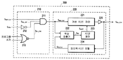
다음으로, 클록 동기화 유닛 (200) 의 비-제한적인 예시적인 일 실시형태가 도 3a를 참조하여 설명된다. 클록 동기화 유닛 (200) 은, 전술한 버퍼링된 클록 신호 SBUF_CLK 및 전술한 소거 또는 프로그램 신호로부터 레퍼런스 클록 신호 SREF_CLK 를 유도하는 클록 제어 회로 (210) 를 포함한다. 클록 제어 회로 (210) 는, 동기화 클록 신호 SDLL_CLK 를 생성하는 지연 록 루프 (DLL) (220) 에 레퍼런스 클록 신호 SREF_CLK 를 피딩한다.Next, one non-limiting exemplary embodiment of
레퍼런스 클록 신호 SREF_CLK 를 생성하기 위해, 클록 제어 회로 (210) 는, 레퍼런스 클록 신호 SREF_CLK 가 버퍼링된 클록 신호 SBUF_CLK 를 추적하는 제 1 동작 상태와 레퍼런스 클록 신호 SREF_CLK 가 버퍼링된 클록 신호 SBUF_CLK 로부터 디커플링되는 제 2 동작 상태 사이에서 제어가능하게 스위칭한다. 소거 또는 프로그램 신호는, 레퍼런스 클록 신호 SREF_CLK 가 버퍼링된 클록 신호 SBUF_CLK 를 추적하는지 또는 그로부터 디커플링되는지에서 역활을 맡는다. 상세하게 그리고 비-제한적인 예시적인 실시형태에 따르면, 클록 제어 회로 (210) 는, 소거 신호 또는 프로그램 신호가 커맨드 프로세싱 유닛 (109) 에 의해 어써트되지 않는 경우, 제 1 동작 상태 (즉, 레퍼런스 클록 신호 SREF_CLK 가 버퍼링된 클록 신호 SBUF_CLK 를 추적함) 로 진입/유지하도록 설계된다. 이와 대조적으로, 클록 제어 회로 (210) 는, 소거 및 프로그램 신호들 중 적어도 하나가 커맨드 프로세싱 유닛 (109) 에 의해 어써트될 경우, 제 2 동작 상태 (즉, 레퍼런스 클록 신호 SREF_CLK 가 버퍼링된 클록 신호 SBUF_CLK 로부터 디커플링됨) 로 진입/유지하도록 설계된다.To generate a reference clock signal S REF_CLK,
따라서, 특정한 비-제한적인 실시형태에서, 클록 제어 회로 (210) 는, AND 로직 게이트 (211) 및 NOR 로직 게이트 (213) 를 포함하도록 설계될 수 있다. NOR 로직 게이트 (213) 는, 커맨드 프로세싱 유닛 (109) 으로부터 소거 및 프로그램 신호들에 의해 피딩된다. AND 로직 게이트 (211) 의 제 1 입력은 버퍼링된 클록 신호 SBUF_CLK 이다. AND 로직 게이트 (211) 의 제 2 입력은, NOR 로직 게이트 (213) 의 출력인 신호 SDLL_EN2 이다. 따라서, 소거 또는 프로그램 신호가 어써트될 경우, NOR 로직 게이트 (213) 는 신호 SDLL_EN2 로 하여금 LOW로 진행하게 하며, 이는 AND 로직 게이트 (211) 를 디스에이블시키고, 그의 출력 신호 (즉, 레퍼런스 클록 신호 SREF_CLK) 로 하여금 LOW로 진행하게 한다. 이것은, 레퍼런스 클록 신호 SREF_CLK 를 버퍼링된 클록 신호 SBUF_CLK 로부터 디커플링시킨다. 한편, 소거 및 프로그램 신호들이 디-어써트될 경우, NOR 로직 게이트 (213) 는 신호 SDLL_EN2 로 하여금 HIGH로 진행하게 하며, 이는, AND 로직 게이트 (211) 를 인에이블시키고, 레퍼런스 클록 신호 SREF_CLK 로 하여금 DLL (220) 에 제공되는 동안, 버퍼링된 클록 신호 SBUF_CLK 를 추적하게 한다.Thus, in certain non-limiting embodiments,
대안의 일 실시형태에서, AND 로직 게이트 (211) 는 3입력 AND 로직 게이트일 수 있으며, 제 3 입력은, 버퍼링된 칩 인에이블 신호 SCEb 에 의해 피딩되는 인버터 로직 게이트 (212) 의 출력에 존재하는 신호 SDLL_EN1 이다. 버퍼링된 칩 인에이블 신호 SCEb 는, 칩 인에이블 포트 (CE#) 에서의 디바이스-외부 신호의 버퍼링된 버전이며, 동일한 극성을 갖는다. 클록 제어 회로 (210) 의 이러한 변형은, 소거 또는 프로그램 신호가 어써트되는지에 관계없이, AND 로직 게이트 (211) 로 하여금, 버퍼링된 칩 인에이블 신호 SCEb 가 LOW로 진행할 때마다 (즉, 비-휘발성 메모리 디바이스 (100) 가 선택될 때마다) 이전에 설명된 바와 같이 동작하게 할 것이지만, 버퍼링된 칩 인에이블 신호 SCEb 가 HIGH로 진행할 때마다 (즉, 비-휘발성 메모리 디바이스 (100) 가 선택해제될 때마다) LOW로 진행하는 AND 로직 게이트 (211) 의 출력을 초래할 것이다.In an alternative embodiment, the AND
또 다른 대안의 실시형태에서, NOR 로직 게이트 (213) 의 기능은 클록 제어 회로 (210) 이외의 다른 곳에서 구현된다. 예를 들어, NOR 로직 게이트 (213) 의 기능은 커맨드 프로세싱 유닛 (109) 에서 구현될 수 있다. 그로서, 커맨드 프로세싱 유닛 (109) 그 자체는, NOR 로직 게이트 (213) 의 출력에 존재하는 것으로 현재 도시되어 있는 신호 SDLL_EN2 를 이슈할 수도 있다.In yet another alternative embodiment, the functionality of the NOR
DLL (220) 은, 레퍼런스 클록 신호 SREF_CLK 에 대한 제어가능한 지연을 갖는 동기화 클록 신호 SDLL_CLK 를 생성하기 위해, 피드백 루프 구성으로 회로 컴포넌트들을 포함한다. 제어가능한 지연은, 동기화 클록 신호 SDLL_CLK 를 수신하는 출력 드라이버 (105) 가 비-휘발성 메모리 디바이스 (100) 에 대한 원하는 타이밍 사양들을 충족시키기 위해, 데이터 라인들 DQ[0:7] 상에서 및 데이터 스트로브 포트 (DQS) 에서 디바이스-외부 신호들을 출력하는 것을 보장하는데 필요한 바와 같이 조정될 수 있다. 필요한 지연을 달성하기 위해, DLL (220) 은, 가변 지연 라인 (221) 을 포함하는 종래의 DLL로서 구현될 수 있다. 가변 지연 라인 (221) 은, 지연 조정 신호 SSHIFT 에 응답하여, 레퍼런스 클록 신호 SREF_CLK 에 대한 동기화 클록 신호 SDLL_CLK 의 지연을 변경시킨다.DLL (220), in order to generate a synchronized clock signal S DLL_CLK having a controllable delay to the reference clock signal REF_CLK S, includes circuit components in a feedback loop configuration. The controllable delay is on the data lines DQ [0: 7] and on the data strobe so that the
피드백 지연 모델 (224) 은, 동기화 클록 신호 SDLL_CLK 에 응답하여 피드백 클록 신호 SFB_CLK 를 생성한다. 피드백 지연 모델 (224) 은, 다음과 같은 몇몇 내부 회로 블록들에 의해 초래된 내부 지연들을 보상하는 복제 지연 모델을 가질 수도 있다.The
- 클록 제어 회로 (210) 내의 AND 로직 게이트 (211);AND
- 입력 클록 포트 (CLK) 에서의 디바이스-외부 신호로부터 버퍼링된 클록 신호 SBUF_CLK 를 출력하는 입력 버퍼 (미도시); 및/또는An input buffer (not shown) which outputs the buffered clock signal S BUF_CLK from the device-external signal at the input clock port CLK; And / or
-데이터 라인들 DQ[0:7] 상에서 및 출력 스트로브 포트 (DQS) 에서의 디바이스-외부 신호들에 대한 출력 버퍼들Output buffers for device-external signals on data lines DQ [0: 7] and at an output strobe port (DQS)
또한, DLL (220) 은, 피드백 클록 신호 SFB_CLK 및 레퍼런스 클록 신호 SREF_CLK 를 수신하며, 그 레퍼런스 클록 신호 SREF_CLK 와 그 피드백 클록 신호 SFB_CLK 사이의 위상 차이를 나타내는 값을 갖는 위상 에러 신호 SPE 를 생성하는 위상 검출기 (222) 를 포함한다. 지연 제어 (223) 는, 위상 검출기 (222) 로부터의 위상 에러 신호 SPE 에 응답하여 지연 조정 신호 SSHIFT 를 생성하며, 가변 지연 라인 (221) 에 의해 적용된 지연을 조정하기 위해 가변 지연 라인 (221) 에 지연 조정 신호 SSHIFT 를 적용한다.In addition, the
위상 검출기 (222) 및 지연 제어 (223) 는, 레퍼런스 클록 신호 SREF_CLK 와 피드백 클록 신호 SFB_CLK 사이의 검출된 위상 차이의 함수로서, 가변 지연 라인 (221) 에 의해 적용된 지연을 조정하도록 협력하여 동작한다. 상세하게, 위상 검출기 (222) 및 지연 제어 (223) 는, 레퍼런스 클록 신호 SREF_CLK 와 피드백 클록 신호 SFB_CLK 사이의 위상 차이가 약 제로가 될 때까지, 동기화 클록 신호 SDLL_CLK 의 가변 지연을 조정하도록 협력하여 동작한다. 더 상세하게, 동기화 클록 신호 SDLL_CLK 의 지연이 조정됨에 따라, 피드백 지연 모델 (224) 로부터의 피드백 클록 신호 SFB_CLK 의 위상은, 피드백 클록 신호 SFB_CLK 가 레퍼런스 클록 신호 SREF_CLK 와 대략적으로 동일한 위상을 가질 때까지, 이에 따라 조정된다. 레퍼런스 클록 신호 SREF_CLK 와 피드백 클록 신호 SFB_CLK 사이의 위상 시프트가 대략적으로 제로와 동일하게 하는 값에 가변 지연을 DLL (220) 이 적용할 경우, DLL (220) 은 "록" 된 것으로 지칭된다. 이러한 때에, 입력 클록 포트 (CLK) 에서의 디바이스-외부 신호 및 동기화 클록 신호 SDLL_CLK 는, 피드백 지연 모델 (224) 이 다양한 내부 지연들을 정확히 모델링한다고 가정하여 동기화될 것이다.
DLL (220) 내의 가변 지연 라인 (221) 이 다수의 지연 스테이지들을 포함할 수도 있으며, 진동 클록 신호가 가변 지연 라인 (221) 을 통해 전파함에 따라 그 지연 스테이지들 모두가 스위칭된다고 고려하면, DLL (220) 이 진동 클록 신호를 피딩받지 않는 시간 동안 전력 절약이 발생할 것이 명백하다. 차례로, 이것은, 상술된 바와 같이 소거 또는 프로그램 신호를 어써트하는 것의 직접적인 결과인, 레퍼런스 클록 신호 SREF_CLK 가 버퍼링된 클록 신호 SBUF_CLK 로부터 디커플링될 경우 발생한다. 따라서, 전체적으로, DLL (220) 에 의해 달성되는 초당 신호 트랜지션의 평균 수는, 레퍼런스 클록 신호 SREF_CLK 가 버퍼링된 클록 신호 SBUF_CLK 를 추적할 경우보다 레퍼런스 클록 신호 SREF_CLK 가 버퍼링된 클록 신호 SBUF_CLK 로부터 디커플링되는 경우 더 적을 것이라는 것이 관측될 것이다. 이것은, 더 높은 클록 신호 주파수들에서 특허 현저한 전력 절약을 초래한다.Considering that the
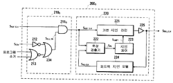
다음으로, 또 다른 비-제한적인 예시적인 실시형태에 따른 클록 동기화 유닛 (200B) 을 도시한 도 3b를 참조한다. 도 3b의 클록 동기화 유닛 (200B) 은, 도 3a의 클록 동기화 유닛 (200) 내의 클록 제어 회로 (210) 와 유사하지만, 다음의 주요한 차이를 갖는 변형된 클록 제어 회로 (210B) 를 포함한다. 상세하게, AND 로직 게이트 (211B) 의 제 2 입력은, 2입력 OR 로직 게이트 (234) 에 의해 출력되는 신호 SDLL_EN 이다. 2입력 OR 로직 게이트 (234) 는, (상기한 바와 같이, 소거 및 프로그램 신호들에 의해 피딩되는) NOR 로직 게이트 (213) 의 출력, 및 (상기한 바와 같이, 버퍼링된 칩 인에이블 신호 SCEb 에 의해 피딩되는) 인버터 로직 게이트 (212) 의 출력에 의해 피딩된다.Next, reference is made to FIG. 3B, which illustrates a
동작에서, 변형된 클록 제어 회로 (210B) 는 AND 로직 게이트 (211B) 로 하여금, 다음의 조건들, 즉, (i) 버퍼링된 칩 인에이블 신호 SCEb 가 LOW 로 진행함 (즉, 비-휘발성 메모리 디바이스 (100) 가 선택될 때마다) 또는 (ii) 소거 및 프로그램 신호들이 디-어써트됨 (= LOW) 중 어느 하나가 충족될 때마다, (레퍼런스 클록 신호 SREF_CLK 를 운반하는) 그의 출력으로 버퍼링된 클록 신호 SBUF_CLK 를 전달하게 한다. 이와 대조적으로, 레퍼런스 클록 신호 SREF_CLK 는, (i) 버퍼링된 칩 인에이블 신호 SCEb 가 HIGH 로 진행할 경우 (즉, 비-휘발성 메모리 디바이스 (100) 가 선택-해제될 때마다) 및 (ii) 소거 또는 프로그램 신호가 어써트될 (= HIGH) 경우 양자의 경우에만 버퍼링된 클록 신호 SBUF_CLK 로부터 디커플링될 것이다. 간단히 말하면, 도 3a의 클록 제어 회로 (210) 와 비교할 경우, 소거 또는 프로그램 신호가 어써트되는 때, 도 3b의 변형된 클록 제어 회로 (210B) 는 버퍼링된 클록 신호 SBUF_CLK 로부터 레퍼런스 클록 신호 SREF_CLK 를 자동적으로 디커플링시키지 않지만, 부가적인 조건을 요구하며, 그에 의해, 비-휘발성 메모리 디바이스 (100) 가 디-어써트된다. 상이하게 언급하면, 비-휘발성 메모리 디바이스 (100) 를 선택하는 것은 DLL (200) 를 활성화시킬 것이며, 따라서, 소거 또는 프로그램 신호의 효과를 오버-라이딩 (over-ride) 할 것이다. 이것은 도 3a의 회로에서보다 더 적은 전력 절약을 유도할 수도 있지만, 그럼에도, 비-휘발성 메모리 디바이스 (100) 의 동작의 더 큰 제어를 제어기 (90) 로부터 직접적으로 허용한다.In operation, modified
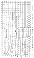
도 4a는, 블록 소거 동작 동안 도 3a의 클록 동기화 유닛 (200) 과 관련된 다양한 신호들의 신호 트랜지션들을 도시한 비-제한적인 예시적인 타이밍도이다. 당업자는, 유사한 타이밍도가 다른 커맨드들 (예를 들어, 페이지 프로그램) 에 대해 제공될 수 있지만, 그들이 판독자가 예시적인 실시형태들의 이해를 획득하는데 요구되지 않는다고 사료되므로 생략됨을 인식할 것이다.4A is a non-limiting exemplary timing diagram illustrating signal transitions of various signals associated with
도 4a의 상부에서의 제어 신호들 (즉, 입력 클록 포트 (CLK), 칩 인에이블 포트 (CE#), 기입/판독 포트 (W/R#), 커맨드 래치 인에이블 포트 (CLE), 어드레스 래치 인에이블 포트 (ALE), 데이터 라인들 DQ[0:7], 데이터 스트로브 포트 (DQS), 및 준비/비지 포트 (R/B#) 에서의 제어 신호들) 은 제어기 (90) 에 의해 이슈된다.Control signals at the top of FIG. 4A (ie, input clock port CLK, chip enable port CE #, write / read port W / R #, command latch enable port CLE, address latch) Enable port ALE, data lines DQ [0: 7], data strobe port DQS, and control signals at ready / busy port R / B #) are issued by
시간 T1 내지 시간 T7 사이에서, 비-휘발성 메모리 디바이스 (100) 는, 블록 소거 커맨드의 제 1 사이클 (60h), 행 어드레스 정보 (RA1, RA2 & RA3), 및 블록 소거 커맨드의 제 2 사이클 (D0h) 을 수신한다. 일단 비-휘발성 메모리 디바이스 (100) 가 블록 소거 커맨드의 제 2 사이클 (D0h) 을 수신 및 디코딩하면, 소거 신호는 시간 T8 에서 어써트되며, (NOR 로직 게이트 (213) 의 출력에서의) SDLL_EN2 신호는 LOW 로 진행한다. 그 후, AND 로직 게이트 (211) 는 SDLL_EN2 신호의 LOW 상태에 의해 디스에이블된다. 따라서, 레퍼런스 클록 신호 SREF_CLK 는 왕복 시간 T8에서 LOW 상태로 진행한다. 그 결과, 동기화 클록 신호 SDLL_CLK 는, 버퍼링된 클록 신호 SBUF_CLK 가 토글링을 유지하더라도 토글링하는 것을 중지한다. 또한, 준비/비지 포트 (R/B#) 신호에서의 디바이스-외부 신호는 LOW 로 진행한다.Between time T1 and time T7, the
그 후, 비-휘발성 메모리 디바이스 (100) 는, 예를 들어, SLC (Single Level Cell) 타입 NAND 플래시 메모리 디바이스에 대해 2ms, 또는 몇몇 타입의 MLC (Multi-Level-Cell) NAND 플래시 메모리 디바이스들에 대해 최대 15ms 일 수 있고 변하는 tBERS (블록 소거 시간) 로서 특정된 시간 동안 비-휘발성 메모리 셀 어레이 (115) 상에서 내부 "소거 및 검증" 동작을 수행한다. 비-휘발성 메모리 디바이스 (100) 가 내부 "소거 및 검증" 동작을 완료하는 시간 동안, DLL (220) 은 효율적으로 디스에이블되며, 따라서, 이러한 시간 동안 인에이블되는 경우보다 더 적은 전력 소비를 초래한다.The
시간 T14 와 시간 T15 사이의 임의의 곳에서, 비-휘발성 메모리 디바이스 (100) 는 그의 최종 "소거 및 검증" 동작을 완료하고, 소거 신호는 LOW 상태로 진행한다. 그 결과, SDLL_EN2 신호는, AND 로직 게이트 (211) 를 인에이블시키는, 시간 T15 에서 HIGH 상태로 다시 진행한다. 따라서, 레퍼런스 클록 신호 SREF_CLK 는 버퍼링된 클록 신호 SBUF_CLK 를 다시 추적하기를 시작하고, DLL (220) 은, 레퍼런스 클록 신호 SREF_CLK 및 피드백 클록 신호 SFB-CLK 에 따라 동기화 클록 신호 SDLL_CLK 를 록하기를 시도한다. 당업자는, DLL (220) 이 지연 록 루프를 포함할 경우, 동기화를 재획득 (즉, "리록 (re-lock)") 하기 위하여 동기화 클록 신호 SDLL_CLK 에 대해 특정 수의 클록 사이클들이 필요할 수도 있음을 인식할 것이다. 도 4a의 타이밍도는, 동기화 클록 신호 SDLL_CLK 가 시간 T16 에서 이미 록되도록 하는 간략화된 짧은 리록 시퀀스를 가정한다. 적절한 리록 시퀀스들이 당업계에 공지되어 있으며, 따라서 여기에서는 설명되지 않는다.Anywhere between time T14 and time T15, the
동기화 클록 신호 SDLL_CLK 가 동기화를 재획득한 이후, 준비/비지 포트 (R/B#) 신호에서의 디바이스-외부 신호는, 시간 T16 과 시간 T17 사이에 도시된 바와 같이 HIGH 로 진행한다. 다음으로, 비-휘발성 메모리 디바이스 (100) 는 "준비" 가 되며, 제어기 (90) 는, 제한이 아니라, 상태 판독, 페이지 판독 및 페이지 프로그램과 같은 또 다른 커맨드를 이슈할 수도 있다.After the synchronization clock signal SDLL_CLK reacquires synchronization, the device-external signal in the ready / busy port (R / B #) signal goes HIGH as shown between time T16 and time T17. Next,
도 4b는, 블록 소거 동작 동안의 도 3b의 클록 동기화 유닛 (200B) 의 신호들에 대한 비-제한적인 예시적인 타이밍도이다. 도 4b의 타이밍도는 도 4a의 타이밍도와 유사하지만, 다음의 예외들을 갖는다. 상세하게, 시간 T7 과 시간 T8 사이에서, 소거 신호가 어써트되더라도, AND 로직 게이트 (211B) 의 제 2 입력에서의 SDLL_EN 신호가 LOW 상태로 드롭되지 않음을 유의한다. 이것은, 버퍼링된 칩 인에이블 신호 SCEb 신호가 여전히 LOW 상태에 있기 (비-휘발성 메모리 디바이스 (100) 는 선택 상태로 유지된다는 것을 의미함) 때문이며, 이러한 실시형태에서, 클록 신호 디커플링 효과를 오버라이딩하고, 그렇지 않으면 소거 신호에 의해 제어된다. 그 후, 칩 인에이블 포트 (CE#) 에서의 디바이스-외부 신호가 (시간 T8 과 시간 T9 사이에서) HIGH 상태로 진행한 이후, 버퍼링된 칩 인에이블 신호 SCEb 또한 HIGH 상태로 진행하며, 다음으로, SDLL_EN 신호가 LOW 상태로 진행한다. 이것은 AND 로직 게이트 (211B) 를 디스에이블시키며, 레퍼런스 클록 신호 SREF_CLK 로 하여금, DLL (220) 이 전력을 불필요하게 소비하지 않도록 토글링하는 것을 중지하게 한다.4B is a non-limiting exemplary timing diagram for the signals of
당업자는, DLL (220) 대신, 클록 동기화 유닛 (200) 이 피드백 루프 구성으로 회로 컴포넌트들을 갖는 다른 모듈들을 이용 및 포함할 수도 있음을 인식할 것이다. 그러한 다른 모듈의 예는 위상-록 루프 (PLL) 이다. 따라서, 위상-록 루프는, 소거 또는 프로그램 신호가 어써트되는 시간 주기 동안 비활성화될 수 있다.Those skilled in the art will appreciate that instead of the
또한, 당업자는, 블록 소거, 페이지 프로그램, 페이지 판독 및 상태 판독 커맨드들의 상기 설명이 단지 예시적일 뿐이며, 다양한 변형들이 본 발명의 실시형태들의 범위를 벗어나지 않고도 가능하다는 것을 인식할 것이다. 또한, 다른 현재 또는 장래의 커맨드들은 소거 및/또는 프로그램 신호들의 어써트를 트리거링할 수도 있다. 예를 들어, 상술된 블록 소거 커맨드와 유사한 가설의 페이지 소거 커맨드의 경우를 고려하지만, 이는, 특정한 멀티-페이지 블록의 단일 페이지로 하여금 그 페이지에서의 다른 블록(들)에 영향을 주지 않으면서 소거되게 한다. 그러한 커맨드의 예는, 여기에 참조로서 포함되는, 발명의 명칭이 "Partial Block Erase Architecture for Flash Memory" 인 Jin-Ki KIM 의 미국 특허 출원 제 11/779,685 호에 설명되어 있다.Moreover, those skilled in the art will recognize that the above description of block erase, page program, page read and status read commands are merely exemplary, and that various modifications are possible without departing from the scope of the embodiments of the present invention. In addition, other current or future commands may trigger the assertion of erase and / or program signals. For example, consider the case of a hypothetical page erase command similar to the block erase command described above, but this allows a single page of a particular multi-page block to be erased without affecting other block (s) in that page. To be. Examples of such commands are described in US Patent Application No. 11 / 779,685 to Jin-Ki KIM, entitled " Partial Block Erase Architecture for Flash Memory ", which is incorporated herein by reference.
상술된 비-휘발성 메모리 디바이스들 (100, 100A) 이, NAND 플래시 EEPROM, NOR 플래시 EEPROM, AND 플래시 EEPROM, DiNOR 플래시 EEPROM, 시리얼 플래시 EEPROM, 판독-전용 메모리 (ROM), 소거가능한 프로그래밍가능 ROM (EPROM), 강유전체 랜덤-액세스 메모리 (FRAM), 자기저항성 RAM (MRAM) 및 위상-변화 RAM (PCRAM) 을 포함하지만 이에 제한되지는 않는 다양한 타입의 비-휘발성 메모리 집적 회로 기술을 사용하여 구현될 수 있음을 이해할 것이다.The
또한, 몇몇 실시형태들에서, 특정한 신호들, 특히 제한이 아닌 클록 신호들 및 데이터 스트로브 신호들은 싱글-엔디드 (single-end) 될 수 있지만, 다른 실시형태들에서, 이들 신호들은 차동일 수 있음을 인식해야 한다.Also, in some embodiments, certain signals, particularly non-limiting clock signals and data strobe signals, may be single-end, but in other embodiments, these signals may be differential. You have to be aware.
또한, 몇몇 실시형태들에서, 특정한 디바이스들, 특히, 입력 레지스터 (112) 및 출력 드라이버 (105) 는, 상승 에지들, 하강 에지들, 또는 상승 에지들 및 하강 에지들 양자에 응답할 수 있으며, 그에 의해, 단일 데이터 레이트 (SDR), 더블 데이터 레이트 (DDR) 또는 쿼더러플 데이터 레이트 (QDR) 기능을 나타냄을 인식해야 한다.Also, in some embodiments, certain devices, in particular,
다시 도 1을 참조하면, 몇몇 예에서, 메모리 시스템 (80) 은, 그 전체 내용이 여기에 참조로서 포함된, "Open NAND Flash Interface Specificatoin", Revision 2.0, Feb. 27/08 에 설명되어 있는 플래시 표준과 적어도 실질적으로 호환될 수도 있다. 다른 예에서, 물론 메모리 시스템 (80) 은, DLL들 및/또는 PLL들을 포함하는 제공 메모리 디바이스들에 부합되는 몇몇 다른 플래시 표준과 적어도 실질적으로 호환될 수도 있다.Referring again to FIG. 1, in some examples,
또한, 몇몇 실시형태들에서, 메모리 디바이스들 (100, 100A) 은, 적어도 부분적으로, 컴퓨터 상에서 구동되는 소프트웨어 프로그램의 사용을 통해 상술된 기능을 제공받을 수 있음을 인식해야 한다. 그러한 소프트웨어 프로그램은 컴퓨터-판독가능 저장 매체 상의 컴퓨터-판독가능 명령들로서 인코딩될 수 있으며, 그 명령들은, 상술된 기능을 달성하기 위해, 상술된 기능을 저-레벨 회로 다이어그램들 및/또는 집적 회로 구성들로 변환하도록 설계된다.In addition, in some embodiments, it should be appreciated that the
설명된 실시형태들의 특정한 적응들 및 변형들이 행해질 수 있다. 따라서, 상술된 실시형태들은 제한이 아닌 예시로 고려된다.Certain adaptations and variations of the described embodiments can be made. Accordingly, the above-described embodiments are to be considered as illustrative and not restrictive.
Claims (74)
- 피드백 루프 구성으로 회로 컴포넌트들을 가지며, 레퍼런스 클록 신호에 의해 구동되는 모듈;
- 상기 레퍼런스 클록 신호가 상기 입력 클록 신호를 추적하는 제 1 동작 상태와 상기 레퍼런스 클록 신호가 상기 입력 클록 신호로부터 디커플링되는 제 2 동작 상태 사이에서 제어가능하게 스위칭할 수 있는 클록 제어 회로; 및
- 상기 제어기에 의해 이슈된 커맨드들을 인식하며, 상기 소거 커맨드를 인식하는 것에 응답하여, 상기 클록 제어 회로로 하여금 상기 제 1 동작 상태로부터 상기 제 2 동작 상태로 스위칭하게 하도록 구성된 커맨드 프로세싱 유닛을 포함하며,
상기 레퍼런스 클록 신호가 상기 입력 클록 신호를 추적할 경우, 상기 모듈은 제 1 양의 전력을 소비하고, 상기 레퍼런스 클록 신호가 상기 입력 클록 신호로부터 디커플링될 경우, 상기 모듈은 상기 제 1 양의 전력보다 적은 제 2 양의 전력을 소비하는, 비-휘발성 반도체 메모리 디바이스.An input port for receiving an input clock signal; And a set of data lines for receiving commands issued by the controller, including an erase command;
A module having circuit components in a feedback loop configuration and driven by a reference clock signal;
Clock control circuitry controllable to switch between a first operating state in which said reference clock signal tracks said input clock signal and a second operating state in which said reference clock signal is decoupled from said input clock signal; And
A command processing unit configured to recognize commands issued by the controller and in response to recognizing the erase command, cause the clock control circuit to switch from the first operating state to the second operating state; ,
When the reference clock signal tracks the input clock signal, the module consumes a first amount of power, and when the reference clock signal is decoupled from the input clock signal, the module is less than the first amount of power. A non-volatile semiconductor memory device that consumes a small second amount of power.
상기 커맨드 프로세싱 유닛이 상기 소거 커맨드를 인식하는 것에 응답하여 상기 비-휘발성 반도체 메모리 디바이스가 비지 (busy) 라는 것을 나타내는 신호를 출력하기 위한 제어 회로를 더 포함하는, 비-휘발성 반도체 메모리 디바이스.The method of claim 1,
And a control circuit for outputting a signal indicating that the non-volatile semiconductor memory device is busy in response to the command processing unit recognizing the erase command.
상기 제어 회로는, 상기 커맨드 프로세싱 유닛이 상기 클록 제어 회로로 하여금 상기 제 1 동작 상태로부터 상기 제 2 동작 상태로 스위칭하게 한 이후 상기 비-휘발성 반도체 메모리 디바이스가 비지라는 것을 나타내는 신호를 출력하도록 구성되는, 비-휘발성 반도체 메모리 디바이스.The method of claim 2,
The control circuit is configured to output a signal indicating that the non-volatile semiconductor memory device is busy after the command processing unit causes the clock control circuit to switch from the first operating state to the second operating state. , Non-volatile semiconductor memory device.
상기 커맨드 프로세싱 유닛은, 상기 소거 커맨드를 인식하는 것에 응답하여 소거 동작을 시작하도록 구성되는, 비-휘발성 반도체 메모리 디바이스.The method of claim 1,
And the command processing unit is configured to start an erase operation in response to recognizing the erase command.
상기 커맨드 프로세싱 유닛은, 상기 소거 동작이 완료된 이후, 상기 클록 제어 회로로 하여금 상기 제 1 동작 상태로 다시 스위칭하게 하도록 구성되는, 비-휘발성 반도체 메모리 디바이스.The method of claim 4, wherein
And the command processing unit is configured to cause the clock control circuit to switch back to the first operating state after the erase operation is completed.
상기 소거 동작이 완료된 이후 상기 비-휘발성 반도체 메모리 디바이스가 준비 상태라는 것을 나타내는 신호를 이슈하도록 구성되는 제어 회로를 더 포함하는, 비-휘발성 반도체 메모리 디바이스.The method of claim 5, wherein
And a control circuit configured to issue a signal indicating that the non-volatile semiconductor memory device is ready after the erase operation is completed.
클록 동기화 회로는, 상기 레퍼런스 클록 신호가 상기 입력 클록 신호로부터 디커플링될 경우 동기화를 손실하는 지연 록 루프를 포함하며,
상기 클록 제어 회로가 상기 제 1 동작 상태로 다시 스위칭된 이후에 상기 지연 록 루프가 동기화를 재획득한 이후, 상기 비-휘발성 반도체 메모리 디바이스가 준비 상태라는 것을 나타내는 신호가 이슈되는, 비-휘발성 반도체 메모리 디바이스.The method according to claim 6,
The clock synchronization circuit includes a delay lock loop that loses synchronization when the reference clock signal is decoupled from the input clock signal,
A non-volatile semiconductor, in which a signal is issued indicating that the non-volatile semiconductor memory device is ready after the delay lock loop regains synchronization after the clock control circuit is switched back to the first operating state Memory device.
상기 커맨드 프로세싱 유닛은, 상기 소거 동작이 완료되기 전에 상기 클록 제어 회로로 하여금 상기 제 1 동작 상태로 다시 스위칭하게 하도록 구성되는, 비-휘발성 반도체 메모리 디바이스.The method of claim 4, wherein
And the command processing unit is configured to cause the clock control circuit to switch back to the first operating state before the erase operation is completed.
상기 커맨드 프로세싱 유닛이 상기 클록 제어 회로로 하여금 상기 제 1 동작 상태로 다시 스위칭하게 한 이후, 상기 비-휘발성 반도체 메모리 디바이스가 준비 상태라는 것을 나타내는 신호를 이슈하도록 구성된 제어 회로를 더 포함하는, 비-휘발성 반도체 메모리 디바이스.The method of claim 8,
Further comprising a control circuit configured to issue a signal indicating that the non-volatile semiconductor memory device is ready after the command processing unit causes the clock control circuit to switch back to the first operating state. Volatile semiconductor memory device.
클록 동기화 회로는, 상기 레퍼런스 클록 신호가 상기 입력 클록 신호로부터 디커플링될 경우 동기화를 손실하는 지연 록 루프를 포함하며,
상기 클록 제어 회로가 상기 제 1 동작 상태로 다시 스위칭된 이후에 상기 지연 록 루프가 동기화를 재획득한 이후, 상기 비-휘발성 반도체 메모리 디바이스가 준비 상태라는 것을 나타내는 신호가 이슈되는, 비-휘발성 반도체 메모리 디바이스.The method of claim 9,
The clock synchronization circuit includes a delay lock loop that loses synchronization when the reference clock signal is decoupled from the input clock signal,
A non-volatile semiconductor, in which a signal is issued indicating that the non-volatile semiconductor memory device is ready after the delay lock loop regains synchronization after the clock control circuit is switched back to the first operating state Memory device.
복수의 비-휘발성 메모리 셀들을 더 포함하며,
상기 커맨드 프로세싱 유닛은 상기 클록 제어 회로로 하여금, 상기 복수의 비-휘발성 메모리 셀들 중 적어도 몇몇이 소거된 이후, 상기 제 1 동작 상태로 다시 스위칭하게 하도록 구성되는, 비-휘발성 반도체 메모리 디바이스.The method of claim 1,
Further comprising a plurality of non-volatile memory cells,
And the command processing unit is configured to cause the clock control circuit to switch back to the first operating state after at least some of the plurality of non-volatile memory cells have been erased.
상기 모듈은, 상기 레퍼런스 클록 신호에 기초하여 동기화 클록 신호를 생성하도록 구성되는 클록 동기화 회로를 포함하는, 비-휘발성 반도체 메모리 디바이스.The method of claim 1,
And the module comprises a clock synchronization circuit configured to generate a synchronization clock signal based on the reference clock signal.
상기 클록 동기화 회로는 지연 록 루프를 포함하는, 비-휘발성 반도체 메모리 디바이스.The method of claim 12,
And the clock synchronization circuit comprises a delay lock loop.
상기 클록 동기화 회로는 위상 록 루프를 포함하는, 비-휘발성 반도체 메모리 디바이스.The method of claim 12,
And the clock synchronization circuit comprises a phase lock loop.
상기 데이터 라인들은, 또한, 상기 비-휘발성 반도체 메모리 디바이스로부터 판독 데이터를 출력하기 위한 것인, 비-휘발성 반도체 메모리 디바이스.The method of claim 12,
And the data lines are further for outputting read data from the non-volatile semiconductor memory device.
상기 동기화 클록 신호와 동기하여 데이터 스트로브 신호를 변경시키도록 구성되는 출력 드라이버를 더 포함하는, 비-휘발성 반도체 메모리 디바이스.The method of claim 15,
And an output driver configured to change a data strobe signal in synchronization with the synchronization clock signal.
상기 출력 드라이버는, 상기 판독 데이터의 출력을 상기 데이터 스트로브 신호와 동기화시키도록 구성되는, 비-휘발성 반도체 메모리 디바이스.17. The method of claim 16,
The output driver is configured to synchronize the output of the read data with the data strobe signal.
상기 인터페이스는, 상기 비-휘발성 반도체 메모리 디바이스로부터 상기 데이터 스트로브 신호를 출력하기 위한 포트를 포함하는, 비-휘발성 반도체 메모리 디바이스.The method of claim 17,
The interface includes a port for outputting the data strobe signal from the non-volatile semiconductor memory device.
상기 클록 제어 회로는, 상기 레퍼런스 클록 신호에 대응하는 출력을 생성하는 로직 AND 기능을 구현하며,
상기 로직 AND 기능은, 상기 입력 클록 신호에 대응하는 제 1 입력, 및 상기 소거 커맨드가 상기 커맨드 프로세싱 유닛에 의해 인식될 경우 어써트되는 신호에 대응하는 제 2 입력을 갖는, 비-휘발성 반도체 메모리 디바이스.The method of claim 1,
The clock control circuit implements a logic AND function that generates an output corresponding to the reference clock signal,
The logic AND function has a first input corresponding to the input clock signal and a second input corresponding to a signal asserted when the erase command is recognized by the command processing unit. .
상기 커맨드들은 상이한 커맨드를 더 포함하며,
상기 커맨드 프로세싱 유닛은 상기 클록 제어 회로로 하여금, 상기 제어기에 의해 이슈된 상기 상이한 커맨드를 인식하는 것에 응답하여 상기 제 1 동작 상태로부터 상기 제 2 동작 상태로 스위칭하게 하도록, 또한, 구성되는, 비-휘발성 반도체 메모리 디바이스.The method of claim 1,
The commands further comprise different commands,
The command processing unit is further configured to cause the clock control circuit to switch from the first operating state to the second operating state in response to recognizing the different command issued by the controller. Volatile semiconductor memory device.
상기 비-휘발성 반도체 메모리 디바이스는, 상기 소거 커맨드가 상기 커맨드 프로세싱 유닛에 의해 인식될 경우 어써트되는 신호에 대응하는 제 1 입력, 및 상기 상이한 커맨드가 상기 커맨드 프로세싱 유닛에 의해 인식될 경우 어써트되는 신호에 대응하는 제 2 입력을 갖는 로직 OR 기능을, 또한, 구현하는, 비-휘발성 반도체 메모리 디바이스.The method of claim 20,
The non-volatile semiconductor memory device is configured to have a first input corresponding to a signal that is asserted when the erase command is recognized by the command processing unit, and asserted when the different command is recognized by the command processing unit. A non-volatile semiconductor memory device, further implementing a logic OR function having a second input corresponding to the signal.
복수의 비-휘발성 메모리 셀들을 더 포함하며,
상기 상이한 커맨드는, 상기 복수의 비-휘발성 메모리 셀들 중 적어도 몇몇을 프로그래밍하기 위한 커맨드인, 비-휘발성 반도체 메모리 디바이스.The method of claim 20,
Further comprising a plurality of non-volatile memory cells,
And the different command is a command for programming at least some of the plurality of non-volatile memory cells.
상기 커맨드 프로세싱 유닛은 상기 클록 제어 회로로 하여금, 상기 복수의 비-휘발성 메모리 셀들 중 적어도 몇몇이 프로그래밍된 이후, 상기 제 1 동작 상태로 다시 스위칭하게 하도록 구성되는, 비-휘발성 반도체 메모리 디바이스.The method of claim 22,
And the command processing unit is configured to cause the clock control circuit to switch back to the first operating state after at least some of the plurality of non-volatile memory cells have been programmed.
상기 상이한 커맨드는 페이지 프로그램 커맨드인, 비-휘발성 반도체 메모리 디바이스.The method of claim 22,
And the different command is a page program command.
상기 인터페이스는, 상기 제어기로부터 디바이스 선택 신호를 수신하기 위한 입력 포트를 포함하며,
상기 디바이스 선택 신호는, 상기 비-휘발성 반도체 메모리 디바이스가 선택 또는 선택해제되는지를 나타내는, 비-휘발성 반도체 메모리 디바이스.The method of claim 1,
The interface includes an input port for receiving a device selection signal from the controller,
And the device select signal indicates whether the non-volatile semiconductor memory device is selected or deselected.
상기 커맨드 프로세싱 유닛은 상기 클록 제어 회로로 하여금, 상기 비-휘발성 반도체 메모리 디바이스가 선택되었다는 것을 상기 디바이스 선택 신호가 나타내는 경우라도, 상기 제 2 동작 상태로 스위칭하게 하도록 구성되는, 비-휘발성 반도체 메모리 디바이스.The method of claim 25,
The command processing unit is configured to cause the clock control circuit to switch to the second operating state even when the device selection signal indicates that the non-volatile semiconductor memory device has been selected. .
상기 커맨드 프로세싱 유닛은, 상기 비-휘발성 반도체 메모리 디바이스가 선택해제되었다는 것을 상기 디바이스 선택 신호가 나타내지 않으면, 상기 클록 제어 회로가 상기 제 2 동작 상태로 스위칭하는 것을 방지하도록 구성되는, 비-휘발성 반도체 메모리 디바이스.The method of claim 25,
The command processing unit is configured to prevent the clock control circuit from switching to the second operating state if the device selection signal does not indicate that the non-volatile semiconductor memory device has been deselected device.
상기 레퍼런스 클록 신호가 상기 입력 클록 신호를 추적할 경우, 상기 모듈은 단위 시간 당 신호 트랜지션의 제 1 평균 수를 달성하고,
상기 레퍼런스 클록 신호가 상기 입력 클록 신호로부터 디커플링될 경우, 상기 모듈은, 상기 단위 시간 당 신호 트랜지션의 제 1 평균 수보다 작은 단위 시간 당 신호 트랜지션의 제 2 평균 수를 달성하는, 비-휘발성 반도체 메모리 디바이스.The method of claim 1,
If the reference clock signal tracks the input clock signal, the module achieves a first average number of signal transitions per unit time,
When the reference clock signal is decoupled from the input clock signal, the module achieves a second average number of signal transitions per unit time less than the first average number of signal transitions per unit time device.
상기 제어기에 의해 이슈된 커맨드들이 인코딩되며,
상기 커맨드 프로세싱 유닛은 디코더를 포함하고,
상기 제어기에 의해 이슈된 특정 커맨드를 인식하기 위해, 상기 디코더는 상기 특정 커맨드를 디코딩하도록 구성되는, 비-휘발성 반도체 메모리 디바이스.The method of claim 1,
Commands issued by the controller are encoded,
The command processing unit comprises a decoder,
And the decoder is configured to decode the specific command to recognize the specific command issued by the controller.
상기 소거 커맨드는 블록 소거 커맨드인, 비-휘발성 반도체 메모리 디바이스.The method of claim 1,
And the erase command is a block erase command.
NAND 플래시 메모리 디바이스로서 구현되는, 비-휘발성 반도체 메모리 디바이스.The method of claim 1,
A non-volatile semiconductor memory device, implemented as a NAND flash memory device.
상기 제어기에 의해 이슈된 커맨드들을 인식하기 위해, 상기 커맨드 프로세싱 유닛은, 상기 데이터 라인들을 통해 수신된 정보를 적어도 하나의 레지스터에 로딩하고, 상기 정보를 상기 커맨드들로 디코딩하도록 구성되는, 비-휘발성 반도체 메모리 디바이스.The method of claim 1,
In order to recognize the commands issued by the controller, the command processing unit is configured to load information received via the data lines into at least one register and to decode the information into the commands. Semiconductor memory device.
- 피드백 루프 구성으로 회로 컴포넌트들을 갖고, 레퍼런스 클록 신호에 의해 구동되는 제 2 수단;
- 상기 레퍼런스 클록 신호가 상기 입력 클록 신호를 추적하는 제 1 동작 상태와 상기 레퍼런스 클록 신호가 상기 입력 클록 신호로부터 디커플링되는 제 2 동작 상태 사이에서 제어가능하게 스위칭하기 위한 제 3 수단;
소거 커맨드를 포함하여 제어기에 의해 이슈된 커맨드들을 인식하고, 상기 소거 커맨드를 인식하는 것에 응답하여 상기 제 3 수단의 동작 상태를 변경시키기 위한 제 4 수단을 포함하며,
상기 레퍼런스 클록 신호가 상기 입력 클록 신호를 추적할 경우, 상기 제 2 수단은 제 1 양의 전력을 소비하고, 상기 레퍼런스 클록 신호가 상기 입력 클록 신호로부터 디커플링될 경우, 상기 제 2 수단은, 상기 제 1 양의 전력보다 적은 제 2 양의 전력을 소비하는, 비-휘발성 반도체 메모리 디바이스.First means for providing an input clock signal;
Second means having circuit components in a feedback loop configuration and driven by a reference clock signal;
Third means for controllably switching between a first operating state in which the reference clock signal tracks the input clock signal and a second operating state in which the reference clock signal is decoupled from the input clock signal;
Fourth means for recognizing commands issued by the controller, including an erase command, and for changing an operating state of the third means in response to recognizing the erase command,
When the reference clock signal tracks the input clock signal, the second means consumes a first amount of power, and when the reference clock signal is decoupled from the input clock signal, the second means comprises: A non-volatile semiconductor memory device consuming a second amount of power less than one amount of power.
- 상기 레퍼런스 클록 신호가 상기 비-휘발성 반도체 메모리 디바이스의 제 1 동작 상태에서 상기 입력 클록 신호를 추적하고, 상기 레퍼런스 클록 신호가 상기 비-휘발성 반도체 메모리 디바이스의 제 2 동작 상태에서 상기 입력 클록 신호로부터 디커플링되도록 상기 레퍼런스 클록 신호를 생성하는 단계로서, 상기 레퍼런스 클록 신호가 상기 입력 클록 신호를 추적할 경우, 상기 모듈은 제 1 양의 전력을 소비하고, 상기 레퍼런스 클록 신호가 상기 입력 클록 신호로부터 디커플링될 경우, 상기 모듈은, 상기 제 1 양의 전력보다 적은 제 2 양의 전력을 소비하는, 상기 레퍼런스 클록 신호를 생성하는 단계; 및
- 상기 비-휘발성 반도체 메모리 디바이스로 하여금, 제어기로부터 수신된 소거 커맨드를 인식하는 것에 응답하여 상기 제 1 동작 상태로부터 상기 제 2 동작 상태로 스위칭하게 하는 단계를 포함하는, 비-휘발성 반도체 메모리 디바이스에 의해 구현되는 방법.A method implemented by a non-volatile semiconductor memory device comprising a module having circuit components driven by a reference clock signal in a feedback loop configuration and receiving an input clock signal, the method comprising:
The reference clock signal tracks the input clock signal in a first operating state of the non-volatile semiconductor memory device, and the reference clock signal is derived from the input clock signal in a second operating state of the non-volatile semiconductor memory device. Generating the reference clock signal to be decoupled, wherein when the reference clock signal tracks the input clock signal, the module consumes a first amount of power and the reference clock signal is decoupled from the input clock signal. If the module is configured to: generate the reference clock signal, consuming a second amount of power less than the first amount of power; And
-Causing the non-volatile semiconductor memory device to switch from the first operating state to the second operating state in response to recognizing an erase command received from a controller. Implemented by.
- 비-휘발성 반도체 메모리 디바이스를 포함하며,
상기 비-휘발성 반도체 메모리 디바이스는,
- 상기 마스터 클록 신호에 관련된 입력 클록 신호를 수신하기 위한 입력 포트; 및 상기 제어기에 의해 이슈된 커맨드들을 수신하기 위한 데이터 라인들의 세트를 포함하는 인터페이스;
- 피드백 루프 구성으로 회로 컴포넌트들을 가지며, 레퍼런스 클록 신호에 의해 구동되는 모듈;
- 상기 레퍼런스 클록 신호가 상기 입력 클록 신호를 추적하는 제 1 동작 상태와 상기 레퍼런스 클록 신호가 상기 입력 클록 신호로부터 디커플링되는 제 2 동작 상태 사이에서 제어가능하게 스위칭할 수 있는 클록 제어 회로; 및
- 상기 제어기에 의해 이슈된 커맨드들을 인식하며, 상기 소거 커맨드를 인식하는 것에 응답하여, 상기 클록 제어 회로로 하여금 상기 제 1 동작 상태로부터 상기 제 2 동작 상태로 스위칭하게 하도록 구성된 커맨드 프로세싱 유닛을 포함하며,
상기 레퍼런스 클록 신호가 상기 입력 클록 신호를 추적할 경우, 상기 모듈은 제 1 양의 전력을 소비하고, 상기 레퍼런스 클록 신호가 상기 입력 클록 신호로부터 디커플링될 경우, 상기 모듈은 상기 제 1 양의 전력보다 적은 제 2 양의 전력을 소비하는, 시스템.A controller configured to issue a master clock signal and issue commands including an erase command; And
A non-volatile semiconductor memory device,
The non-volatile semiconductor memory device,
An input port for receiving an input clock signal associated with said master clock signal; And a set of data lines for receiving commands issued by the controller;
A module having circuit components in a feedback loop configuration and driven by a reference clock signal;
Clock control circuitry controllable to switch between a first operating state in which said reference clock signal tracks said input clock signal and a second operating state in which said reference clock signal is decoupled from said input clock signal; And
A command processing unit configured to recognize commands issued by the controller and in response to recognizing the erase command, cause the clock control circuit to switch from the first operating state to the second operating state; ,
When the reference clock signal tracks the input clock signal, the module consumes a first amount of power, and when the reference clock signal is decoupled from the input clock signal, the module is less than the first amount of power. The system consumes a small second amount of power.
상기 기능은,
- 레퍼런스 클록 신호가 상기 비-휘발성 반도체 메모리 디바이스의 제 1 동작 상태에서 입력 클록 신호를 추적하고, 상기 레퍼런스 클록 신호가 상기 비-휘발성 반도체 메모리 디바이스의 제 2 동작 상태에서 상기 입력 클록 신호로부터 디커플링되도록 상기 레퍼런스 클록 신호를 생성하는 기능으로서, 상기 레퍼런스 클록 신호가 상기 입력 클록 신호를 추적할 경우, 피드백 루프 구성으로 회로 컴포넌트들을 갖고 상기 레퍼런스 클록 신호에 의해 구동되는 모듈에 의해 제 1 양의 전력이 소비되고, 상기 레퍼런스 클록 신호가 상기 입력 클록 신호로부터 디커플링될 경우, 상기 모듈은, 상기 제 1 양의 전력보다 적은 제 2 양의 전력을 소비하는, 상기 레퍼런스 클록 신호를 생성하는 기능; 및
- 상기 비-휘발성 반도체 메모리 디바이스로 하여금, 제어기로부터 수신된 소거 커맨드를 인식하는 것에 응답하여 상기 제 1 동작 상태로부터 상기 제 2 동작 상태로 스위칭하게 하는 기능을 포함하는, 컴퓨터-판독가능 저장 매체.When processed, a computer-readable storage medium comprising computer-readable instructions used to provide a non-volatile semiconductor memory device with the following functions:
The function is
A reference clock signal tracks an input clock signal in a first operating state of the non-volatile semiconductor memory device and the reference clock signal is decoupled from the input clock signal in a second operating state of the non-volatile semiconductor memory device. Generating the reference clock signal, wherein when the reference clock signal tracks the input clock signal, a first amount of power is consumed by a module having circuit components in a feedback loop configuration and driven by the reference clock signal. And when the reference clock signal is decoupled from the input clock signal, the module further comprises: generating the reference clock signal, consuming a second amount of power less than the first amount of power; And
-Causing the non-volatile semiconductor memory device to switch from the first operating state to the second operating state in response to recognizing an erase command received from a controller.
회로 컴포넌트들을 갖고 단자를 갖춘 기능성 모듈;
노드;
상기 단자가 상기 노드에 전기적으로 접속되는 제 1 동작 상태와 상기 단자가 상기 노드로부터 전기적으로 디커플링되는 제 2 동작 상태 사이에서 제어가능하게 스위칭할 수 있는 스위칭가능 회로로서, 상기 노드는, 상기 스위칭가능 회로가 상기 제 1 동작 상태에 있는 경우, 상기 노드를 통해 전달되는 상기 기능성 모듈에 대한 신호를 갖도록 구성되는, 상기 스위칭가능 회로; 및
상기 제어기에 의해 이슈된 커맨드들을 인식하며, 상기 소거 커맨드를 인식하는 것에 응답하여, 상기 스위칭가능 회로로 하여금 상기 제 1 동작 상태로부터 상기 제 2 동작 상태로 스위칭하게 하도록 구성되는 커맨드 프로세싱 유닛을 포함하는, 비-휘발성 반도체 메모리 디바이스.An interface for receiving commands issued by the controller, including an erase command;
A functional module having circuit components and having a terminal;
Node;
A switchable circuit that can controllably switch between a first operating state in which the terminal is electrically connected to the node and a second operating state in which the terminal is electrically decoupled from the node, the node being switchable. The switchable circuit configured to have a signal for the functional module passed through the node when the circuit is in the first operating state; And
A command processing unit configured to recognize commands issued by the controller and to cause the switchable circuitry to switch from the first operating state to the second operating state in response to recognizing the erase command. , Non-volatile semiconductor memory device.
상기 회로 컴포넌트들은 피드백 루프 구성으로 존재하며,
상기 기능성 모듈에 대한 신호는, 상기 단자가 상기 노드에 전기적으로 접속될 경우 상기 기능성 모듈의 동작을 동기화시키기 위한 입력 클록 신호를 포함하는, 비-휘발성 반도체 메모리 디바이스.39. The method of claim 37,
The circuit components are in a feedback loop configuration,
And the signal to the functional module comprises an input clock signal for synchronizing operation of the functional module when the terminal is electrically connected to the node.
상기 인터페이스는 데이터 라인들의 세트를 포함하며,
상기 커맨드들은 상기 데이터 라인들의 세트를 통해 수신되는, 비-휘발성 반도체 메모리 디바이스.The method of claim 38,
The interface includes a set of data lines,
And the commands are received via the set of data lines.
상기 단자가 상기 노드에 전기적으로 접속될 경우, 상기 모듈은 제 1 양의 전력을 소비하고, 상기 단자가 상기 노드로부터 전기적으로 디커플링될 경우, 상기 모듈은, 상기 제 1 양의 전력보다 작은 제 2 양의 전력을 소비하는, 비-휘발성 반도체 메모리 디바이스.The method of claim 38,
When the terminal is electrically connected to the node, the module consumes a first amount of power, and when the terminal is electrically decoupled from the node, the module is: a second less than the first amount of power. A non-volatile semiconductor memory device consuming a positive amount of power.
상기 커맨드 프로세싱 유닛이 상기 소거 커맨드를 인식하는 것에 응답하여 상기 비-휘발성 반도체 메모리 디바이스가 비지라는 것을 나타내는 신호를 출력하기 위한 제어 회로를 더 포함하는, 비-휘발성 반도체 메모리 디바이스.The method of claim 38,
And a control circuit for outputting a signal indicating that the non-volatile semiconductor memory device is busy in response to the command processing unit recognizing the erase command.
상기 제어 회로는, 상기 커맨드 프로세싱 유닛이 상기 스위칭가능 회로로 하여금 상기 제 1 동작 상태로부터 상기 제 2 동작 상태로 스위칭하게 한 이후 상기 비-휘발성 반도체 메모리 디바이스가 비지라는 것을 나타내는 신호를 출력하도록 구성되는, 비-휘발성 반도체 메모리 디바이스.42. The method of claim 41 wherein
The control circuit is configured to output a signal indicating that the non-volatile semiconductor memory device is busy after the command processing unit causes the switchable circuit to switch from the first operating state to the second operating state. , Non-volatile semiconductor memory device.
상기 커맨드 프로세싱 유닛은, 상기 소거 커맨드를 인식하는 것에 응답하여 소거 동작을 시작하도록 구성되는, 비-휘발성 반도체 메모리 디바이스.The method of claim 38,
And the command processing unit is configured to start an erase operation in response to recognizing the erase command.
상기 커맨드 프로세싱 유닛은 상기 스위칭가능 회로로 하여금, 상기 소거 동작이 완료된 이후 상기 제 1 동작 상태로 다시 스위칭하게 하도록 구성되는, 비-휘발성 반도체 메모리 디바이스.The method of claim 43,
And the command processing unit is configured to cause the switchable circuit to switch back to the first operating state after the erase operation is completed.
상기 소거 동작이 완료된 이후 상기 비-휘발성 반도체 메모리 디바이스가 준비 상태라는 것을 나타내는 신호를 이슈하도록 구성되는 제어 회로를 더 포함하는, 비-휘발성 반도체 메모리 디바이스.45. The method of claim 44,
And a control circuit configured to issue a signal indicating that the non-volatile semiconductor memory device is ready after the erase operation is completed.
상기 회로 컴포넌트들은, 상기 단자가 상기 노드로부터 전기적으로 디커플링될 경우 동기화를 손실하는 지연 록 루프를 구현하며,
상기 스위칭가능 회로가 상기 제 1 동작 상태로 다시 스위칭한 이후에 상기 지연 록 루프가 동기화를 재획득한 이후, 상기 비-휘발성 반도체 메모리 디바이스가 준비 상태라는 것을 나타내는 신호가 이슈되는, 비-휘발성 반도체 메모리 디바이스.The method of claim 45,
The circuit components implement a delay lock loop that loses synchronization when the terminal is electrically decoupled from the node,
A non-volatile semiconductor, in which a signal is issued indicating that the non-volatile semiconductor memory device is ready after the delay lock loop regains synchronization after the switchable circuit has switched back to the first operating state Memory device.
상기 커맨드 프로세싱 유닛은 상기 스위칭가능 회로로 하여금, 상기 소거 동작이 완료되기 전에 상기 제 1 동작 상태로 다시 스위칭하게 하도록 구성되는, 비-휘발성 반도체 메모리 디바이스.The method of claim 43,
And the command processing unit is configured to cause the switchable circuit to switch back to the first operating state before the erase operation is completed.
상기 커맨드 프로세싱 유닛이 상기 스위칭가능 회로로 하여금 상기 제 1 동작 상태로 다시 스위칭하게 한 이후, 상기 비-휘발성 반도체 메모리 디바이스가 준비 상태라는 것을 나타내는 신호를 이슈하도록 구성되는 제어 회로를 더 포함하는, 비-휘발성 반도체 메모리 디바이스.The method of claim 47,
And further including a control circuit configured to issue a signal indicating that the non-volatile semiconductor memory device is ready after the command processing unit causes the switchable circuit to switch back to the first operating state. -Volatile semiconductor memory device.
상기 회로 컴포넌트들은, 상기 단자가 상기 노드로부터 전기적으로 디커플링될 경우 동기화를 손실하는 지연 록 루프를 구현하며,
상기 스위칭가능 회로가 상기 제 1 동작 상태로 다시 스위칭한 이후에 상기 지연 록 루프가 동기화를 재획득한 이후, 상기 비-휘발성 반도체 메모리 디바이스가 준비 상태라는 것을 나타내는 신호가 이슈되는, 비-휘발성 반도체 메모리 디바이스.49. The method of claim 48 wherein
The circuit components implement a delay lock loop that loses synchronization when the terminal is electrically decoupled from the node,
A non-volatile semiconductor, in which a signal is issued indicating that the non-volatile semiconductor memory device is ready after the delay lock loop regains synchronization after the switchable circuit has switched back to the first operating state Memory device.
복수의 비-휘발성 메모리 셀들을 더 포함하며,
상기 커맨드 프로세싱 유닛은 상기 스위칭가능 회로로 하여금, 상기 비-휘발성 메모리 셀들 중 적어도 몇몇이 소거된 이후, 상기 제 1 동작 상태로 다시 스위칭하게 하도록 구성되는, 비-휘발성 반도체 메모리 디바이스.The method of claim 38,
Further comprising a plurality of non-volatile memory cells,
And the command processing unit is configured to cause the switchable circuit to switch back to the first operating state after at least some of the non-volatile memory cells are erased.
상기 기능성 모듈의 회로 컴포넌트들은, 상기 단자에서의 신호에 기초하여 동기화 클록 신호를 생성하도록 구성된 클록 동기화 회로를 구현하는, 비-휘발성 반도체 메모리 디바이스.The method of claim 38,
Circuit components of the functional module implement a clock synchronization circuit configured to generate a synchronized clock signal based on the signal at the terminal.
상기 클록 동기화 회로는 지연 록 루프를 포함하는, 비-휘발성 반도체 메모리 디바이스.The method of claim 51 wherein
And the clock synchronization circuit comprises a delay lock loop.
상기 클록 동기화 회로는 위상 록 루프를 포함하는, 비-휘발성 반도체 메모리 디바이스.The method of claim 51 wherein
And the clock synchronization circuit comprises a phase lock loop.
상기 인터페이스는, 또한, 상기 비-휘발성 반도체 메모리 디바이스로부터 판독 데이터를 출력하기 위한 것인, 비-휘발성 반도체 메모리 디바이스.The method of claim 51 wherein
And the interface is further for outputting read data from the non-volatile semiconductor memory device.
상기 동기화 클록 신호와 동기하여 데이터 스트로브 신호를 변경시키도록 구성된 출력 드라이버를 더 포함하는, 비-휘발성 반도체 메모리 디바이스.The method of claim 54, wherein
And an output driver configured to change a data strobe signal in synchronization with the synchronization clock signal.
상기 출력 드라이버는, 상기 판독 데이터의 출력을 상기 데이터 스트로브 신호와 동기화시키도록 구성되는, 비-휘발성 반도체 메모리 디바이스.The method of claim 55,
The output driver is configured to synchronize the output of the read data with the data strobe signal.
상기 인터페이스는, 상기 비-휘발성 반도체 메모리 디바이스로부터 데이터 스트로브 신호를 출력하기 위한 포트를 포함하는, 비-휘발성 반도체 메모리 디바이스.The method of claim 56, wherein
And the interface includes a port for outputting a data strobe signal from the non-volatile semiconductor memory device.
상기 스위칭가능 회로는 상기 단자에서 출력을 생성하는 로직 AND 기능을 구현하며,
상기 로직 AND 기능은, 상기 입력 클록 신호에 대응하는 제 1 입력, 및 상기 소거 커맨드가 상기 커맨드 프로세싱 유닛에 의해 인식될 경우 어써트되는 신호에 대응하는 제 2 입력을 갖는, 비-휘발성 반도체 메모리 디바이스.The method of claim 38,
The switchable circuit implements a logic AND function that generates an output at the terminal,
The logic AND function has a first input corresponding to the input clock signal and a second input corresponding to a signal asserted when the erase command is recognized by the command processing unit. .
상기 제어기에 의해 이슈된 커맨드들은 상이한 커맨드를 더 포함하며,
상기 커맨드 프로세싱 유닛은 상기 스위칭가능 회로로 하여금, 상기 제어기에 의해 이슈된 상이한 커맨드를 인식하는 것에 응답하여 상기 동작 상태로부터 상기 제 2 동작 상태로 스위칭하게 하도록, 또한, 구성되는, 비-휘발성 반도체 메모리 디바이스.The method of claim 38,
The commands issued by the controller further comprise different commands,
The command processing unit is further configured to cause the switchable circuitry to switch from the operating state to the second operating state in response to recognizing a different command issued by the controller. device.
상기 비-휘발성 반도체 메모리 디바이스는, 또한, 상기 소거 커맨드가 상기 커맨드 프로세싱 유닛에 의해 인식될 경우 어써트되는 신호에 대응하는 제 1 입력, 및 상기 상이한 커맨드가 상기 커맨드 프로세싱 유닛에 의해 인식될 경우 어써트되는 신호에 대응하는 제 2 입력을 갖는 로직 OR 기능을 구현하는, 비-휘발성 반도체 메모리 디바이스.The method of claim 59,
The non-volatile semiconductor memory device may also have a first input corresponding to a signal that is asserted when the erase command is recognized by the command processing unit, and a first input when the different command is recognized by the command processing unit. A non-volatile semiconductor memory device that implements a logic OR function having a second input corresponding to the signal being written.
복수의 비-휘발성 메모리 셀들을 더 포함하며,
상기 상이한 커맨드는, 상기 비-휘발성 메모리 셀들 중 적어도 일부를 프로그래밍하기 위한 커맨드인, 비-휘발성 반도체 메모리 디바이스.The method of claim 59,
Further comprising a plurality of non-volatile memory cells,
And the different command is a command for programming at least some of the non-volatile memory cells.
상기 커맨드 프로세싱 유닛은 상기 스위칭가능 회로로 하여금, 상기 비-휘발성 메모리 셀들 중 적어도 일부가 프로그래밍된 이후 상기 제 1 동작 상태로 다시 스위칭하게 하도록, 또한, 구성되는, 비-휘발성 반도체 메모리 디바이스.62. The method of claim 61,
And the command processing unit is further configured to cause the switchable circuit to switch back to the first operating state after at least some of the non-volatile memory cells have been programmed.
상기 상이한 커맨드는 페이지 프로그램 커맨드인, 비-휘발성 반도체 메모리 디바이스.62. The method of claim 61,
And the different command is a page program command.
상기 인터페이스는 상기 제어기로부터 디바이스 선택 신호를 수신하기 위한 입력 포트를 포함하며,
상기 디바이스 선택 신호는, 상기 비-휘발성 반도체 메모리 디바이스가 선택 또는 선택해제되는지를 나타내는, 비-휘발성 반도체 메모리 디바이스.The method of claim 38,
The interface includes an input port for receiving a device selection signal from the controller,
And the device select signal indicates whether the non-volatile semiconductor memory device is selected or deselected.
상기 커맨드 프로세싱 유닛은 상기 스위칭가능 회로로 하여금, 상기 디바이스 선택 신호가 상기 비-휘발성 반도체 메모리 디바이스가 선택되었다고 나타내는 경우라도 상기 제 2 동작 상태로 스위칭하게 하도록, 또한, 구성되는, 비-휘발성 반도체 메모리 디바이스.The method of claim 64, wherein
The command processing unit is further configured to cause the switchable circuit to switch to the second operating state even when the device selection signal indicates that the non-volatile semiconductor memory device has been selected. device.
상기 커맨드 프로세싱 유닛은, 상기 디바이스 선택 신호가 상기 비-휘발성 반도체 메모리 디바이스가 선택해제되었다고 나타내지 않으면, 상기 스위칭가능 회로가 상기 제 2 동작 상태로 스위칭하는 것을 방지하도록, 또한, 구성되는, 비-휘발성 반도체 메모리 디바이스.The method of claim 64, wherein
The command processing unit is further configured to prevent the switchable circuit from switching to the second operating state unless the device selection signal indicates that the non-volatile semiconductor memory device is deselected. Semiconductor memory device.
상기 단자가 상기 노드에 전기적으로 접속될 경우, 상기 기능성 모듈의 회로 컴포넌트들은 단위 시간당 신호 트랜지션의 제 1 평균 수를 수행하고, 상기 단자가 상기 노드로부터 전기적으로 디커플링될 경우, 상기 기능성 모듈의 회로 컴포넌트들은, 상기 단위 시간당 신호 트랜지션의 제 1 평균 수보다 적은 단위 시간당 신호 트랜지션의 제 2 평균 수를 수행하는, 비-휘발성 반도체 메모리 디바이스.The method of claim 38,
When the terminal is electrically connected to the node, the circuit components of the functional module perform a first average number of signal transitions per unit time, and when the terminal is electrically decoupled from the node, the circuit component of the functional module. And perform a second average number of signal transitions per unit time less than the first average number of signal transitions per unit time.
상기 제어기에 의해 이슈된 커맨드들은 코딩된 신호들로 인코딩되며,
상기 커맨드 프로세싱 유닛은, 특정 코딩된 신호가 상기 소거 커맨드를 인코딩할 경우, 상기 특정 코딩된 신호로부터 상기 소거 커맨드를 추출하도록 구성된 디코더를 포함하는, 비-휘발성 반도체 메모리 디바이스.The method of claim 38,
Commands issued by the controller are encoded into coded signals,
And the command processing unit comprises a decoder configured to extract the erase command from the specific coded signal when the specific coded signal encodes the erase command.
상기 소거 커맨드는 블록 소거 커맨드인, 비-휘발성 반도체 메모리 디바이스.39. The method of claim 37,
And the erase command is a block erase command.
NAND 플래시 메모리 디바이스로서 구현되는, 비-휘발성 반도체 메모리 디바이스.The method of claim 38,
A non-volatile semiconductor memory device, implemented as a NAND flash memory device.
상기 제어기에 의해 이슈된 커맨드들을 인식하기 위해, 상기 커맨드 프로세싱 유닛은, 상기 인터페이스를 통해 수신된 정보를 적어도 하나의 레지스터에 로딩하고, 상기 정보를 상기 커맨드들로 디코딩하도록 구성되는, 비-휘발성 반도체 메모리 디바이스.The method of claim 38,
In order to recognize the commands issued by the controller, the command processing unit is configured to load information received via the interface into at least one register and to decode the information into the commands. Memory device.
- 상기 비-휘발성 반도체 메모리 디바이스로 하여금 제어기로부터 수신된 소거 커맨드를 인식하는 것에 응답하여 제 1 동작 상태로부터 제 2 동작 상태로 스위칭하게 하는 단계;
- 상기 비-휘발성 반도체 메모리 디바이스가 상기 제 1 동작 상태에 있는 경우, 상기 노드에 상기 단자를 전기적으로 접속시키는 단계; 및
- 상기 비-휘발성 반도체 메모리 디바이스가 상기 제 2 동작 상태에 있는 경우, 상기 노드로부터 상기 단자를 전기적으로 디커플링시키는 단계를 포함하는, 비-휘발성 반도체 메모리 디바이스에 의해 구현되는 방법.A method implemented by a non-volatile semiconductor memory device comprising a node and a functional module having circuit components and terminals, the method comprising:
Causing the non-volatile semiconductor memory device to switch from a first operating state to a second operating state in response to recognizing an erase command received from a controller;
Electrically connecting the terminal to the node when the non-volatile semiconductor memory device is in the first operating state; And
Electrically decoupling the terminal from the node when the non-volatile semiconductor memory device is in the second operating state.
상기 컴퓨터-판독가능 명령들은,
- 제어기로부터 수신된 소거 커맨드를 인식하는 것에 응답하여 제 1 동작 상태로부터 제 2 동작 상태로 스위칭하기 위한 기능;
- 상기 비-휘발성 반도체 메모리 디바이스가 상기 제 1 동작 상태에 있는 경우, 상기 노드에 상기 단자를 전기적으로 접속시키기 위한 기능; 및
- 상기 비-휘발성 반도체 메모리 디바이스가 상기 제 2 동작 상태에 있는 경우, 상기 노드로부터 상기 단자를 전기적으로 디커플링시키기 위한 기능을 갖는, 컴퓨터-판독가능 저장 매체.A computer-readable storage medium comprising computer-readable instructions used to produce a non-volatile semiconductor memory device comprising a node and a functional module having circuit components and terminals when processed, comprising:
The computer-readable instructions are as follows:
A function for switching from the first operating state to the second operating state in response to recognizing an erase command received from the controller;
A function for electrically connecting the terminal to the node when the non-volatile semiconductor memory device is in the first operating state; And
A non-volatile semiconductor memory device having the function to electrically decouple the terminal from the node when the non-volatile semiconductor memory device is in the second operating state.
- 비-휘발성 반도체 메모리 디바이스를 포함하며,
상기 비-휘발성 반도체 메모리 디바이스는,
- 상기 제어기에 의해 이슈된, 상기 소거 커맨드들을 포함하는 커맨드들을 수신하기 위한 인터페이스;
- 회로 컴포넌트들을 갖고 단자를 갖춘 기능성 모듈;
- 노드;
- 상기 단자가 상기 노드에 전기적으로 접속되는 제 1 동작 상태와 상기 단자가 상기 노드로부터 전기적으로 디커플링되는 제 2 동작 상태 사이에서 제어가능하게 스위칭할 수 있는 스위칭가능 회로로서, 상기 노드는, 상기 스위칭가능 회로가 상기 제 1 동작 상태에 있는 경우, 상기 노드를 통해 전달된 상기 기능성 모듈에 대한 신호를 갖도록 구성되는, 상기 스위칭가능 회로; 및
- 상기 제어기에 의해 이슈된 커맨드들을 인식하며, 상기 소거 커맨드를 인식하는 것에 응답하여, 상기 스위칭가능 회로로 하여금 상기 제 1 동작 상태로부터 상기 제 2 동작 상태로 스위칭하게 하도록 구성되는 커맨드 프로세싱 유닛을 포함하는, 시스템.A controller configured to issue commands including an erase command; And
A non-volatile semiconductor memory device,
The non-volatile semiconductor memory device,
An interface for receiving commands, including the erase commands, issued by the controller;
A functional module with circuit components and equipped with terminals;
A node;
A switchable circuit capable of controllably switching between a first operating state in which the terminal is electrically connected to the node and a second operating state in which the terminal is electrically decoupled from the node, wherein the node comprises: the switching The switchable circuitry configured to have a signal for the functional module passed through the node when an enabler circuit is in the first operating state; And
A command processing unit configured to recognize commands issued by the controller and in response to recognizing the erase command, cause the switchable circuitry to switch from the first operating state to the second operating state. System.
Applications Claiming Priority (4)
| Application Number | Priority Date | Filing Date | Title |
|---|---|---|---|
| US1572407P | 2007-12-21 | 2007-12-21 | |
| US61/015,724 | 2007-12-21 | ||
| US4873708P | 2008-04-29 | 2008-04-29 | |
| US61/048,737 | 2008-04-29 |
Publications (1)
| Publication Number | Publication Date |
|---|---|
| KR20100106410A true KR20100106410A (en) | 2010-10-01 |
Family
ID=40790102
Family Applications (1)
| Application Number | Title | Priority Date | Filing Date |
|---|---|---|---|
| KR1020107013633A KR20100106410A (en) | 2007-12-21 | 2008-09-15 | Non-volatile semiconductor memory device with power saving feature |
Country Status (8)
| Country | Link |
|---|---|
| US (2) | US8145925B2 (en) |
| EP (1) | EP2223301A4 (en) |
| JP (1) | JP5574972B2 (en) |
| KR (1) | KR20100106410A (en) |
| CN (1) | CN101903953B (en) |
| CA (1) | CA2701180A1 (en) |
| TW (1) | TW200937420A (en) |
| WO (1) | WO2009079744A1 (en) |
Families Citing this family (22)
| Publication number | Priority date | Publication date | Assignee | Title |
|---|---|---|---|---|
| US11948629B2 (en) * | 2005-09-30 | 2024-04-02 | Mosaid Technologies Incorporated | Non-volatile memory device with concurrent bank operations |
| US7277357B1 (en) * | 2006-06-05 | 2007-10-02 | Micron Technology, Inc. | Method and apparatus for reducing oscillation in synchronous circuits |
| US8291248B2 (en) | 2007-12-21 | 2012-10-16 | Mosaid Technologies Incorporated | Non-volatile semiconductor memory device with power saving feature |
| US8145925B2 (en) * | 2007-12-21 | 2012-03-27 | Mosaid Technologies Incorporated | Non-volatile semiconductor memory device with power saving feature |
| US9223642B2 (en) * | 2013-03-15 | 2015-12-29 | Super Talent Technology, Corp. | Green NAND device (GND) driver with DRAM data persistence for enhanced flash endurance and performance |
| US8843692B2 (en) | 2010-04-27 | 2014-09-23 | Conversant Intellectual Property Management Inc. | System of interconnected nonvolatile memories having automatic status packet |
| JP2013200830A (en) * | 2012-03-26 | 2013-10-03 | Toshiba Corp | Memory system |
| US9471484B2 (en) | 2012-09-19 | 2016-10-18 | Novachips Canada Inc. | Flash memory controller having dual mode pin-out |
| KR20150098649A (en) | 2012-12-22 | 2015-08-28 | 퀄컴 인코포레이티드 | Reducing power consumption of volatile memory via use of non-volatile memory |
| TWI508099B (en) | 2013-01-28 | 2015-11-11 | Phison Electronics Corp | Clock switching meyhod, memory controller and memory storage apparatus |
| US9443602B2 (en) | 2013-08-23 | 2016-09-13 | Kabushiki Kaisha Toshiba | Storage device and data latch timing adjustment method |
| JP6440481B2 (en) * | 2014-12-15 | 2018-12-19 | ルネサスエレクトロニクス株式会社 | Semiconductor device |
| US10176403B2 (en) * | 2016-05-24 | 2019-01-08 | Morphotrust Usa, Llc | Shape detection |
| CN106158032A (en) * | 2016-06-30 | 2016-11-23 | 深圳市航顺芯片技术研发有限公司 | For the erasing of eeprom memory and write circuit and method thereof |
| CN106158012B (en) * | 2016-07-05 | 2019-07-16 | 深圳市紫光同创电子有限公司 | Timing sequence process method, on-chip SRAM and the FPGA of FPGA on-chip SRAM |
| US10331517B2 (en) * | 2016-08-26 | 2019-06-25 | Qualcomm Incorporated | Link error correction in memory system |
| CN108268085B (en) * | 2017-01-03 | 2023-05-26 | 三星电子株式会社 | Semiconductor device with a semiconductor device having a plurality of semiconductor chips |
| KR102493964B1 (en) | 2017-12-18 | 2023-02-01 | 삼성전자주식회사 | Storage controller, storage device including the same, and operation method of storage controller |
| US10558594B2 (en) * | 2018-05-24 | 2020-02-11 | Essencecore Limited | Memory device, the control method of the memory device and the method for controlling the memory device |
| TWI697099B (en) * | 2018-05-24 | 2020-06-21 | 香港商艾思科有限公司 | Memory device and control method thereof, and method of controlling memory device |
| CN109140670A (en) * | 2018-08-03 | 2019-01-04 | 广东美的暖通设备有限公司 | Control method, system and the air conditioner of the data write-in of EEPROM |
| US11004499B1 (en) | 2020-05-08 | 2021-05-11 | Winbond Electronics Corp. | Latency control circuit and method |
Family Cites Families (90)
| Publication number | Priority date | Publication date | Assignee | Title |
|---|---|---|---|---|
| US5167024A (en) | 1989-09-08 | 1992-11-24 | Apple Computer, Inc. | Power management for a laptop computer with slow and sleep modes |
| US5333300A (en) | 1991-02-11 | 1994-07-26 | Intel Corporation | Timing circuitry and method for controlling automated programming and erasing of a non-volatile semiconductor memory |
| US5430859A (en) | 1991-07-26 | 1995-07-04 | Sundisk Corporation | Solid state memory system including plural memory chips and a serialized bus |
| US5313429A (en) | 1992-02-14 | 1994-05-17 | Catalyst Semiconductor, Inc. | Memory circuit with pumped voltage for erase and program operations |
| US5583457A (en) | 1992-04-14 | 1996-12-10 | Hitachi, Ltd. | Semiconductor integrated circuit device having power reduction mechanism |
| KR960000616B1 (en) | 1993-01-13 | 1996-01-10 | 삼성전자주식회사 | Non-volatile semiconductor memory device |
| US5452259A (en) | 1993-11-15 | 1995-09-19 | Micron Technology Inc. | Multiport memory with pipelined serial input |
| US5526311A (en) | 1993-12-30 | 1996-06-11 | Intel Corporation | Method and circuitry for enabling and permanently disabling test mode access in a flash memory device |
| US5696917A (en) | 1994-06-03 | 1997-12-09 | Intel Corporation | Method and apparatus for performing burst read operations in an asynchronous nonvolatile memory |
| US5796673A (en) | 1994-10-06 | 1998-08-18 | Mosaid Technologies Incorporated | Delay locked loop implementation in a synchronous dynamic random access memory |
| JP3592386B2 (en) | 1994-11-22 | 2004-11-24 | 株式会社ルネサステクノロジ | Synchronous semiconductor memory device |
| US5765002A (en) | 1995-03-13 | 1998-06-09 | Intel Corporation | Method and apparatus for minimizing power consumption in a microprocessor controlled storage device |
| KR960039006A (en) * | 1995-04-26 | 1996-11-21 | 김광호 | Nonvolatile semiconductor memory device connectable to DRAM bus |
| US5742840A (en) | 1995-08-16 | 1998-04-21 | Microunity Systems Engineering, Inc. | General purpose, multiple precision parallel operation, programmable media processor |
| JPH09212411A (en) * | 1996-02-06 | 1997-08-15 | Tokyo Electron Ltd | Memory system |
| US5973552A (en) | 1996-11-04 | 1999-10-26 | Mosaid Technologies Incorporated | Power savings technique in solid state integrated circuits |
| US6216233B1 (en) * | 1997-02-12 | 2001-04-10 | Intel Corporation | Maintaining a memory while in a power management mode |
| CA2204089C (en) | 1997-04-30 | 2001-08-07 | Mosaid Technologies Incorporated | Digital delay locked loop |
| US5903496A (en) | 1997-06-25 | 1999-05-11 | Intel Corporation | Synchronous page-mode non-volatile memory with burst order circuitry |
| JPH1116349A (en) * | 1997-06-26 | 1999-01-22 | Mitsubishi Electric Corp | Synchronous semiconductor memory device |
| JPH11116349A (en) * | 1997-08-11 | 1999-04-27 | Honda Motor Co Ltd | Fiber-reinforced ceramic molded product and sintered product |
| US6442644B1 (en) | 1997-08-11 | 2002-08-27 | Advanced Memory International, Inc. | Memory system having synchronous-link DRAM (SLDRAM) devices and controller |
| JP4039532B2 (en) | 1997-10-02 | 2008-01-30 | 株式会社ルネサステクノロジ | Semiconductor integrated circuit device |
| US5848026A (en) * | 1997-12-08 | 1998-12-08 | Atmel Corporation | Integrated circuit with flag register for block selection of nonvolatile cells for bulk operations |
| JP4006072B2 (en) * | 1997-12-16 | 2007-11-14 | 富士通株式会社 | Semiconductor integrated circuit device |
| JP4060442B2 (en) * | 1998-05-28 | 2008-03-12 | 富士通株式会社 | Memory device |
| US6208542B1 (en) | 1998-06-30 | 2001-03-27 | Sandisk Corporation | Techniques for storing digital data in an analog or multilevel memory |
| JP2000030448A (en) | 1998-07-15 | 2000-01-28 | Mitsubishi Electric Corp | Synchronous semiconductor storage |
| JP3880206B2 (en) * | 1998-07-16 | 2007-02-14 | 富士通株式会社 | Integrated circuit device |
| JP2000036192A (en) * | 1998-07-17 | 2000-02-02 | Fujitsu Ltd | Semiconductor integrated circuit |
| KR100686681B1 (en) | 1999-02-01 | 2007-02-27 | 가부시키가이샤 히타치세이사쿠쇼 | Semiconductor integrated circuit and nonvolatile memory element |
| JP4397076B2 (en) * | 1999-08-20 | 2010-01-13 | 株式会社ルネサステクノロジ | Semiconductor device |
| US6205084B1 (en) * | 1999-12-20 | 2001-03-20 | Fujitsu Limited | Burst mode flash memory |
| KR100355229B1 (en) | 2000-01-28 | 2002-10-11 | 삼성전자 주식회사 | Semiconductor memory device capable of operating delay performace of CAS command |
| US6728798B1 (en) | 2000-07-28 | 2004-04-27 | Micron Technology, Inc. | Synchronous flash memory with status burst output |
| JP4798843B2 (en) * | 2000-09-01 | 2011-10-19 | ルネサスエレクトロニクス株式会社 | Semiconductor device |
| JP3923715B2 (en) * | 2000-09-29 | 2007-06-06 | 株式会社東芝 | Memory card |
| JP2002132375A (en) * | 2000-10-19 | 2002-05-10 | Yamaha Corp | Clock signal control circuit |
| EP1225597A1 (en) | 2001-01-15 | 2002-07-24 | STMicroelectronics S.r.l. | Synchronous-reading nonvolatile memory |
| US6438060B1 (en) | 2001-02-12 | 2002-08-20 | Micron Technology, Inc. | Method of reducing standby current during power down mode |
| JP2002358795A (en) * | 2001-05-31 | 2002-12-13 | Hitachi Ltd | Non-volatile semiconductor storage device and manufacturing method |
| US6570791B2 (en) | 2001-08-30 | 2003-05-27 | Micron Technology, Inc. | Flash memory with DDRAM interface |
| US6605969B2 (en) | 2001-10-09 | 2003-08-12 | Micron Technology, Inc. | Method and circuit for adjusting the timing of ouput data based on an operational mode of output drivers |
| JP2003123488A (en) * | 2001-10-11 | 2003-04-25 | Toshiba Corp | Semiconductor memory |
| JP3799269B2 (en) * | 2001-12-10 | 2006-07-19 | 株式会社東芝 | Nonvolatile semiconductor memory device |
| US6677804B2 (en) | 2002-02-11 | 2004-01-13 | Micron Technology, Inc. | Dual bandgap voltage reference system and method for reducing current consumption during a standby mode of operation and for providing reference stability during an active mode of operation |
| JP4095317B2 (en) | 2002-03-14 | 2008-06-04 | 富士通株式会社 | Asynchronous semiconductor memory device, asynchronous semiconductor memory device internal control method and system |
| US6621762B1 (en) * | 2002-05-29 | 2003-09-16 | Micron Technology, Inc. | Non-volatile delay register |
| US6809990B2 (en) | 2002-06-21 | 2004-10-26 | Micron Technology, Inc. | Delay locked loop control circuit |
| US6707747B2 (en) | 2002-07-08 | 2004-03-16 | Micron Technology, Inc. | Dynamic input thresholds for semiconductor devices |
| US6650594B1 (en) * | 2002-07-12 | 2003-11-18 | Samsung Electronics Co., Ltd. | Device and method for selecting power down exit |
| CN1679109B (en) | 2002-08-28 | 2011-06-15 | Nxp股份有限公司 | Method for reducing power consumption in a state retaining circuit, state retaining circuit and electronic device |
| KR100471182B1 (en) * | 2002-09-03 | 2005-03-10 | 삼성전자주식회사 | Semiconductor memory device informing internal voltage level using ready/busy pin |
| JP2004110906A (en) * | 2002-09-17 | 2004-04-08 | Renesas Technology Corp | Semiconductor memory |
| US6850458B2 (en) | 2002-11-14 | 2005-02-01 | Wen Li | Controlling data strobe output |
| JP4005909B2 (en) * | 2002-12-26 | 2007-11-14 | スパンション インク | Semiconductor memory device and method for controlling semiconductor memory device |
| US7308524B2 (en) | 2003-01-13 | 2007-12-11 | Silicon Pipe, Inc | Memory chain |
| US6791889B2 (en) | 2003-02-04 | 2004-09-14 | Intel Corporation | Double data rate memory interface |
| JP4326294B2 (en) * | 2003-09-16 | 2009-09-02 | 株式会社ルネサステクノロジ | Semiconductor memory device |
| US6975556B2 (en) * | 2003-10-09 | 2005-12-13 | Micron Technology, Inc. | Circuit and method for controlling a clock synchronizing circuit for low power refresh operation |
| KR100590855B1 (en) | 2003-10-14 | 2006-06-19 | 주식회사 하이닉스반도체 | Semiconductor memory device for reducing current consumption |
| JP4386706B2 (en) * | 2003-11-06 | 2009-12-16 | 富士通マイクロエレクトロニクス株式会社 | Semiconductor memory device |
| US7031221B2 (en) | 2003-12-30 | 2006-04-18 | Intel Corporation | Fixed phase clock and strobe signals in daisy chained chips |
| KR100966895B1 (en) * | 2004-01-06 | 2010-06-30 | 삼성전자주식회사 | Apparatus for testing nonvolatile memory and the method thereof |
| JP4583043B2 (en) * | 2004-02-13 | 2010-11-17 | 凸版印刷株式会社 | Semiconductor memory |
| US7227383B2 (en) | 2004-02-19 | 2007-06-05 | Mosaid Delaware, Inc. | Low leakage and data retention circuitry |
| KR100632944B1 (en) * | 2004-05-31 | 2006-10-12 | 삼성전자주식회사 | Non-volatile memory device capable of changing increment of program voltage according to mode of operation |
| US7382178B2 (en) | 2004-07-09 | 2008-06-03 | Mosaid Technologies Corporation | Systems and methods for minimizing static leakage of an integrated circuit |
| US7078950B2 (en) | 2004-07-20 | 2006-07-18 | Micron Technology, Inc. | Delay-locked loop with feedback compensation |
| JP2006065922A (en) * | 2004-08-25 | 2006-03-09 | Toshiba Corp | Semiconductor memory apparatus |
| US7583115B2 (en) | 2004-08-26 | 2009-09-01 | Micron Technology, Inc. | Delay line off-state control with power reduction |
| US7177208B2 (en) | 2005-03-11 | 2007-02-13 | Micron Technology, Inc. | Circuit and method for operating a delay-lock loop in a power saving manner |
| US7561896B2 (en) * | 2005-07-27 | 2009-07-14 | Samsung Electronics Co., Ltd. | Method and system for origination signaling in a wireless network |
| KR100762259B1 (en) | 2005-09-12 | 2007-10-01 | 삼성전자주식회사 | Nand flash memory device with burst read latency function |
| JP4999302B2 (en) * | 2005-09-15 | 2012-08-15 | 凸版印刷株式会社 | Semiconductor memory |
| US20070076502A1 (en) | 2005-09-30 | 2007-04-05 | Pyeon Hong B | Daisy chain cascading devices |
| US7292061B2 (en) | 2005-09-30 | 2007-11-06 | Masaid Technologies Incorporated | Semiconductor integrated circuit having current leakage reduction scheme |
| WO2007036050A1 (en) | 2005-09-30 | 2007-04-05 | Mosaid Technologies Incorporated | Memory with output control |
| US7411429B2 (en) | 2005-10-28 | 2008-08-12 | Silicon Integrated Systems Corp. | System and method for clock switching |
| US7430676B2 (en) * | 2006-03-03 | 2008-09-30 | Apple, Inc. | Method and apparatus for changing the clock frequency of a memory system |
| US7366028B2 (en) | 2006-04-24 | 2008-04-29 | Sandisk Corporation | Method of high-performance flash memory data transfer |
| DE102006023173B4 (en) * | 2006-05-17 | 2012-07-19 | Qimonda Ag | Integrated semiconductor memory with clock generation and method for operating an integrated semiconductor memory |
| US7701764B2 (en) * | 2006-05-17 | 2010-04-20 | Micron Technology, Inc. | Apparatus and method for reduced peak power consumption during common operation of multi-NAND flash memory devices |
| JP2008097715A (en) * | 2006-10-12 | 2008-04-24 | Elpida Memory Inc | Semiconductor memory and memory module |
| US7752364B2 (en) | 2006-12-06 | 2010-07-06 | Mosaid Technologies Incorporated | Apparatus and method for communicating with semiconductor devices of a serial interconnection |
| KR101494023B1 (en) | 2007-02-16 | 2015-02-16 | 컨버전트 인텔렉츄얼 프로퍼티 매니지먼트 인코포레이티드 | Semiconductor device and method for reducing power consumption in a system having interconnected devices |
| US7804718B2 (en) * | 2007-03-07 | 2010-09-28 | Mosaid Technologies Incorporated | Partial block erase architecture for flash memory |
| US7865756B2 (en) | 2007-03-12 | 2011-01-04 | Mosaid Technologies Incorporated | Methods and apparatus for clock signal synchronization in a configuration of series-connected semiconductor devices |
| US8145925B2 (en) * | 2007-12-21 | 2012-03-27 | Mosaid Technologies Incorporated | Non-volatile semiconductor memory device with power saving feature |
| US8291248B2 (en) | 2007-12-21 | 2012-10-16 | Mosaid Technologies Incorporated | Non-volatile semiconductor memory device with power saving feature |
-
2008
- 2008-09-15 US US12/210,580 patent/US8145925B2/en active Active
- 2008-09-15 KR KR1020107013633A patent/KR20100106410A/en active IP Right Grant
- 2008-09-15 EP EP08800326A patent/EP2223301A4/en not_active Withdrawn
- 2008-09-15 CN CN2008801214087A patent/CN101903953B/en not_active Expired - Fee Related
- 2008-09-15 CA CA2701180A patent/CA2701180A1/en not_active Abandoned
- 2008-09-15 WO PCT/CA2008/001623 patent/WO2009079744A1/en active Application Filing
- 2008-09-15 JP JP2010538286A patent/JP5574972B2/en not_active Expired - Fee Related
- 2008-12-17 TW TW097149198A patent/TW200937420A/en unknown
-
2012
- 2012-02-29 US US13/408,252 patent/US8359485B2/en active Active
Also Published As
| Publication number | Publication date |
|---|---|
| US20120159055A1 (en) | 2012-06-21 |
| JP2011507140A (en) | 2011-03-03 |
| TW200937420A (en) | 2009-09-01 |
| US20090164830A1 (en) | 2009-06-25 |
| CN101903953A (en) | 2010-12-01 |
| WO2009079744A1 (en) | 2009-07-02 |
| US8359485B2 (en) | 2013-01-22 |
| JP5574972B2 (en) | 2014-08-20 |
| US8145925B2 (en) | 2012-03-27 |
| EP2223301A1 (en) | 2010-09-01 |
| CN101903953B (en) | 2013-12-18 |
| EP2223301A4 (en) | 2012-04-04 |
| CA2701180A1 (en) | 2009-07-02 |
Similar Documents
| Publication | Publication Date | Title |
|---|---|---|
| US8359485B2 (en) | Non-volatile semiconductor memory device with power saving feature | |
| US9213389B2 (en) | Non-volatile semiconductor memory device with power-saving feature | |
| US11880569B2 (en) | Clock mode determination in a memory system | |
| CN106374916B (en) | Timing control all-digital DLL control circuit and NAND FLash controller control method | |
| KR100721021B1 (en) | Burst read circuit in semiconductor memory device and burst read method thereof | |
| US8074040B2 (en) | Flash device and method for improving performance of flash device | |
| CN110534147B (en) | Memory device, method of controlling the same, and method of controlling the same | |
| CN115798534A (en) | Data output control circuit and semiconductor device including the same | |
| KR20230049921A (en) | Latch circuit, transmission circuit including the transmission circuit and semiconductor apparatus including the transmission circuit |
Legal Events
| Date | Code | Title | Description |
|---|---|---|---|
| A201 | Request for examination | ||
| E902 | Notification of reason for refusal | ||
| E701 | Decision to grant or registration of patent right |