KR20100105388A - Method for fabricating light emitting diode divice and light emitting diode package and light emitting diode module and lamp device having the same - Google Patents
Method for fabricating light emitting diode divice and light emitting diode package and light emitting diode module and lamp device having the same Download PDFInfo
- Publication number
- KR20100105388A KR20100105388A KR1020100020856A KR20100020856A KR20100105388A KR 20100105388 A KR20100105388 A KR 20100105388A KR 1020100020856 A KR1020100020856 A KR 1020100020856A KR 20100020856 A KR20100020856 A KR 20100020856A KR 20100105388 A KR20100105388 A KR 20100105388A
- Authority
- KR
- South Korea
- Prior art keywords
- emitting diode
- light emitting
- lower mold
- chip
- package
- Prior art date
Links
Images


Classifications
-
- F—MECHANICAL ENGINEERING; LIGHTING; HEATING; WEAPONS; BLASTING
- F21—LIGHTING
- F21K—NON-ELECTRIC LIGHT SOURCES USING LUMINESCENCE; LIGHT SOURCES USING ELECTROCHEMILUMINESCENCE; LIGHT SOURCES USING CHARGES OF COMBUSTIBLE MATERIAL; LIGHT SOURCES USING SEMICONDUCTOR DEVICES AS LIGHT-GENERATING ELEMENTS; LIGHT SOURCES NOT OTHERWISE PROVIDED FOR
- F21K9/00—Light sources using semiconductor devices as light-generating elements, e.g. using light-emitting diodes [LED] or lasers
- F21K9/90—Methods of manufacture
-
- F—MECHANICAL ENGINEERING; LIGHTING; HEATING; WEAPONS; BLASTING
- F21—LIGHTING
- F21V—FUNCTIONAL FEATURES OR DETAILS OF LIGHTING DEVICES OR SYSTEMS THEREOF; STRUCTURAL COMBINATIONS OF LIGHTING DEVICES WITH OTHER ARTICLES, NOT OTHERWISE PROVIDED FOR
- F21V19/00—Fastening of light sources or lamp holders
- F21V19/001—Fastening of light sources or lamp holders the light sources being semiconductors devices, e.g. LEDs
- F21V19/0015—Fastening arrangements intended to retain light sources
- F21V19/0025—Fastening arrangements intended to retain light sources the fastening means engaging the conductors of the light source, i.e. providing simultaneous fastening of the light sources and their electric connections
-
- H—ELECTRICITY
- H01—ELECTRIC ELEMENTS
- H01L—SEMICONDUCTOR DEVICES NOT COVERED BY CLASS H10
- H01L33/00—Semiconductor devices with at least one potential-jump barrier or surface barrier specially adapted for light emission; Processes or apparatus specially adapted for the manufacture or treatment thereof or of parts thereof; Details thereof
- H01L33/48—Semiconductor devices with at least one potential-jump barrier or surface barrier specially adapted for light emission; Processes or apparatus specially adapted for the manufacture or treatment thereof or of parts thereof; Details thereof characterised by the semiconductor body packages
- H01L33/52—Encapsulations
- H01L33/54—Encapsulations having a particular shape
-
- H—ELECTRICITY
- H01—ELECTRIC ELEMENTS
- H01L—SEMICONDUCTOR DEVICES NOT COVERED BY CLASS H10
- H01L33/00—Semiconductor devices with at least one potential-jump barrier or surface barrier specially adapted for light emission; Processes or apparatus specially adapted for the manufacture or treatment thereof or of parts thereof; Details thereof
- H01L33/48—Semiconductor devices with at least one potential-jump barrier or surface barrier specially adapted for light emission; Processes or apparatus specially adapted for the manufacture or treatment thereof or of parts thereof; Details thereof characterised by the semiconductor body packages
- H01L33/58—Optical field-shaping elements
-
- F—MECHANICAL ENGINEERING; LIGHTING; HEATING; WEAPONS; BLASTING
- F21—LIGHTING
- F21Y—INDEXING SCHEME ASSOCIATED WITH SUBCLASSES F21K, F21L, F21S and F21V, RELATING TO THE FORM OR THE KIND OF THE LIGHT SOURCES OR OF THE COLOUR OF THE LIGHT EMITTED
- F21Y2115/00—Light-generating elements of semiconductor light sources
- F21Y2115/10—Light-emitting diodes [LED]
Abstract
Description
The present invention relates to a method of manufacturing a light emitting diode device, a light emitting diode package, a light emitting diode module, and a lighting fixture having the same. More specifically, a molding part or a lens part covering a light emitting diode chip is formed using a vacuum sealing method. The present invention relates to a method of manufacturing a light emitting diode device having a variety of light distribution structures by fabricating a dome shape, a light emitting diode package, a light emitting diode module, and a lighting fixture having the same.
In general, a light emitting diode (LED) is a kind of pn junction diode, and when a voltage is applied in a forward direction, a semiconductor using an electroluminescence effect is a phenomenon in which a mono-chromatic light is emitted. Element.
That is, when the forward voltage is applied, the electrons of the n-layer and the holes of the p-layer are combined to emit energy corresponding to the energy difference between the conduction band and the valence band, which is light. If it is emitted in the form of LED will be.
On the other hand, LED packaging is divided into a lamp type (Lamp type) and a surface-mounting device (SMD) packaging.
1 and 2 are views illustrating a general light emitting diode package. As shown in FIGS. 1 and 2, a general surface mount
3 is a perspective view showing a general light emitting diode module, and as shown in FIG. 3, the light
In this state, when the switch is operated in the "ON" state, the light
Such a light emitting diode module can be used for a relatively long time compared to a conventional lighting lamp such as a fluorescent lamp or a halogen / incandescent lamp, has a very low power consumption, a very bright brightness, instantaneous lighting without safety, and excellent safety. In addition, since it can be produced in various colors, its application range is very wide, and it is becoming a light bulb to replace a conventional light bulb.
However, in the conventional light emitting diode module formed as described above, a lens made of poly methyl methacrylate (PMMA) material after mounting the light
In particular, light sources such as halogen lamps, fluorescent lamps, incandescent lamps, etc., which are mainly used in the conventional lighting lamps, have a lot of power consumption, have limitations in color implementation, and have a short lifespan.
Accordingly, in recent years, a light emitting diode device is rapidly changing to a trend of replacing a light source used in the related art.
In particular, lighting lamps require various types of light distribution structures, but the conventional LED module displays the highest luminance value only in the vertical plane of the installation direction. There is a problem that the radiation angle control means is required, there is a problem that it is difficult to implement various types of light distribution (配 光).
According to the embodiment of the present invention, the molding part encapsulating the light emitting diode chip and the lens part encapsulating the light emitting diode package are formed in a non-dome shape instead of a traditional dome shape so that light is distributed in a direction determined according to the design. Provided are a light emitting diode package and a light emitting diode module having various light distribution structures, and lighting fixtures using the same.
Embodiments of the present invention provide a method of manufacturing a light emitting diode package and a light emitting diode module that can easily and quickly produce a light emitting diode package and a module having various light distribution using a vacuum sealing method.
A method of manufacturing a light emitting diode device according to an embodiment of the present invention includes the steps of: providing a chip assembly mounted with at least one LED chip; Inverting the chip assembly, mounting the upper mold to an upper mold, and placing the chip assembly in a first vacuum processor; Injecting a lower mold into the second vacuum processor and filling the molding resin into at least one resin filling portion formed in the lower mold; Injecting the lower mold into a first vacuum processor and placing the lower mold below the upper mold; Coupling the upper mold and the lower mold such that the molding resin encapsulates the light emitting diode chip of the chip assembly; Curing the molding resin to form a non-dom shaped molding in the chip assembly; Separating the chip assembly from the upper mold and the lower mold. In particular, after the step of separating the chip assembly includes a dicing step of cutting the chip assembly into at least one unit package.
In addition, a method of manufacturing a light emitting diode device according to another embodiment of the present invention includes providing a substrate assembly on which at least one light emitting diode package is mounted; Inverting and mounting the substrate assembly to an upper mold and feeding the first vacuum processor into the first vacuum processor; Injecting a lower mold into the second vacuum processor and filling the molding resin into at least one resin filling portion formed in the lower mold; Injecting the lower mold into a first vacuum processor and placing the lower mold below the upper mold; Coupling the upper mold and the lower mold such that the molding resin encapsulates the LED package of the substrate assembly; Curing the molding resin to form a non-dome lens portion in the substrate assembly; Separating the package assembly from the upper mold and the lower mold.
In the filling of the molding resin into the resin filling portion of the lower mold, the resin filling portion formed in the lower mold is characterized in that it has a non-dome shape in which the groove is formed.
The filling of the molding resin into the resin filling part of the lower mold is characterized in that the molding resin is filled by a printing method or a dispenser method.
The molding resin is characterized in that the light transmissive silicone resin or epoxy resin.
A light emitting diode package according to an embodiment of the present invention includes a chip assembly mounted with at least one light emitting diode chip; The light emitting diode chip is encapsulated, and grooves having a predetermined width are formed along a center line in a radial direction to disperse light on the surface, and the first transmission surface and the second transmission surface having different inclinations are formed on left and right sides of the groove portion. It is formed symmetrically with respect to the center portion, the front and rear ends of the groove portion includes a molding portion in which the third transmission surface having a predetermined width and inclination is formed to be inclined. In particular, the first transmission surface has a semi-circular or semi-elliptic shape, and the second transmission surface has a shape in which the width of the center is narrow and wider as the distance from the center to both sides is wider.
According to another embodiment of the present invention, a light emitting diode package includes: a chip assembly having at least one light emitting diode chip mounted thereon; The light emitting diode chip is encapsulated, and a plurality of groove portions formed in a radial direction so as to disperse light are provided at predetermined intervals to form a wave pattern.
The chip assembly includes a base plate; At least two electrodes spaced apart from each other on the base plate, characterized in that the light emitting diode chip is electrically connected to the electrode.
According to an embodiment of the present invention, a light emitting diode module includes: a substrate assembly having at least one light emitting diode package mounted thereon; At least one recess is formed to encapsulate the light emitting diode package and to disperse light on the surface, and at least one of the edges of the recess includes a lens portion having an opening having a lower height than other edges of the recess.
The substrate assembly may include a printed circuit board formed on a predetermined electrode pattern, and the light emitting diode package may be electrically connected to the electrode pattern.
According to an embodiment of the present invention, the molding part encapsulating the light emitting diode chip and the lens part encapsulating the light emitting diode package are manufactured in a non-dome shape instead of a traditional dome shape to form various light distribution structures. Therefore, the light generated from the light emitting diode chip can be distributed and irradiated in a direction determined according to the design.
Accordingly, it is possible to provide various types of light emitting diode modules and lighting fixtures having a light distribution structure desired by the consumer.
In addition, since the non-dom shaped molding part or the lens part is formed by a vacuum sealing method using a mold having a predetermined shape, a process of removing bubbles contained in the molding resin forming the molding part and the lens part separately and a process of mounting the lens are provided. As there is no application, it is possible to manufacture LED packages and modules easily and quickly, thereby reducing the production cost and improving the production yield.
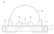
1 is a cross-sectional view showing a typical light emitting diode package,
2 is a perspective view showing a typical light emitting diode package,
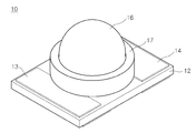
3 is a perspective view showing a general light emitting diode module,
4 is a cross-sectional view showing a light emitting diode package according to an embodiment of the present invention.
5 is a perspective view showing a light emitting diode package according to an embodiment of the present invention;
6 is a perspective view showing a light emitting diode package according to another embodiment of the present invention,
7 is a perspective view showing a light emitting diode module according to an embodiment of the present invention;
8A to 8H are views illustrating a method of manufacturing a light emitting diode package according to an embodiment of the present invention.
9A to 9D are views illustrating a method of manufacturing a light emitting diode module according to an embodiment of the present invention.
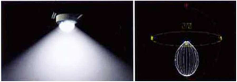
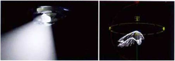
10A is an experimental result of finding a light directivity angle for a conventional LED package,
10B is an experimental result of finding a light directivity angle for the LED package according to the embodiment of the present invention.
Hereinafter, with reference to the accompanying drawings will be described an embodiment of the present invention in more detail. It will be apparent to those skilled in the art that the present invention may be embodied in many different forms and should not be construed as limited to the embodiments set forth herein. Rather, these embodiments are provided so that this disclosure will be thorough and complete, It is provided to let you know. Like numbers refer to like elements in the figures.
In the description of the present invention, the light emitting diode device is used to include both the light emitting diode package and the light emitting diode module.
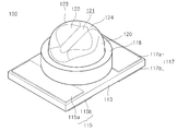
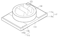
Figure 4 is a cross-sectional view showing a light emitting diode package according to an embodiment of the present invention, Figure 5 is a perspective view showing a light emitting diode package according to an embodiment of the present invention, Figure 6 is a light emitting according to another embodiment of the present invention A perspective view showing a diode package.
As shown in FIGS. 4 and 5, a light emitting diode package according to an embodiment of the present invention includes a
The
The
The light emitting
The
In addition, as shown in FIG. 6, the
As such, the shape of the
In this case, the molding resin forming the
A
The
Next, a light emitting diode module according to an embodiment of the present invention will be described with reference to FIG. 7.
As shown in FIG. 7, the
The light emitting
The
The
Next, a method of manufacturing a light emitting diode package according to an embodiment of the present invention will be described with reference to FIGS. 8A to 8H.
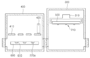
8A to 8I are views illustrating a method of manufacturing a light emitting diode package according to an embodiment of the present invention, and as shown in the drawing, a method of manufacturing a light emitting diode package according to an embodiment of the present invention is as follows. .
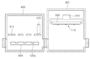
First, an apparatus for manufacturing a light emitting diode package according to an embodiment of the present invention by a vacuum sealing method will be described. In this embodiment, a method of supplying a molding resin by a printing method of the vacuum sealing method will be described as an example.
The vacuum seal facility includes at least two vacuum processors 300,400. Thus, in the
In order to manufacture a light emitting diode package using the above-mentioned vacuum sealing facility, first, a
As shown in FIG. 8B, the
Then, as shown in FIG. 8C, the
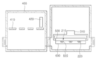
When the
As shown in FIG. 8E, the
Then, the
In addition, a predetermined time, preferably a time that the
When the curing of the
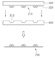
In addition, the
As described above, the
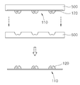
Next, a method of manufacturing a light emitting diode module according to an embodiment of the present invention will be described with reference to the drawings.
9A to 9D are views illustrating a method of manufacturing a light emitting diode module according to an embodiment of the present invention.
The manufacturing method of the LED module is similarly applied to the vacuum sealing method and the mold press method used in the above-described method of manufacturing the LED package. Accordingly, duplicate description will be omitted or simplified. However, the shape of the
In the method of manufacturing a light emitting diode module according to an embodiment of the present invention, first, as shown in FIG. 9A, a
Then, the
Next, as shown in FIG. 9B, the
In addition, a predetermined time, preferably a time when the
When the curing of the
Next, the light directing angle of the light emitting diode package according to the exemplary embodiment of the present invention is compared by comparing the light directing angle of the conventional LED package and the light emitting diode package according to the exemplary embodiment of the present invention.
FIG. 10A is an experimental result of finding a light directivity angle with respect to a conventional LED package, and FIG. 10B is a test result of finding a light directivity angle with respect to the LED package according to an embodiment of the present invention.
As can be seen in FIG. 10A, a light emitting diode package having a conventional domed molding part is uniformly irradiated with a constant light directing angle, and as shown in FIG. 10B, a non-dome type according to an embodiment of the present invention. It can be seen that the LED package having a molding part is irradiated with light as much as desired by the user by dispersing light and desired light direction. Therefore, it can be seen that the shape of the non-dome-shaped molding part can be modified to implement a desired light directing angle.
The light emitting diode package and the light emitting diode module manufactured as described above are manufactured in package and module units, respectively, and applied to various fields. For example, a light emitting diode package having a non-dom shaped molding part manufactured according to the present invention may be mounted on a printed circuit board to form a light emitting diode module. It is used as a light source. In addition, at least one light emitting diode module having a non-dome lens part manufactured according to the present invention is arranged and used as a light source of a lighting fixture.
Although the light emitting diode package and the light emitting diode module illustrated in the present invention have been described as an example of being manufactured by surface-mounted packaging, the present invention is not limited thereto. will be. For example, it may be applied to lamp type LED packaging.
Although described above with reference to the drawings and embodiments, those skilled in the art can be variously modified and changed within the scope of the invention without departing from the spirit of the invention described in the claims below. I can understand.
100: light emitting diode package 110: chip assembly
111: LED chip 113: base plate
115,117: electrode 118: casing
119: wire 120: molding part
121: groove 200: light emitting diode module
210: substrate assembly 211: printed circuit board
220: lens portion 221: groove portion
Claims (14)
Inverting the chip assembly, mounting the upper mold to an upper mold, and placing the chip assembly in a first vacuum processor;
Injecting a lower mold into the second vacuum processor and filling the molding resin into at least one resin filling portion formed in the lower mold;
Injecting the lower mold into a first vacuum processor and placing the lower mold below the upper mold;
Coupling the upper mold and the lower mold such that the molding resin encapsulates the light emitting diode chip of the chip assembly;
Curing the molding resin to form a non-dom shaped molding in the chip assembly;
And separating the chip assembly from the upper mold and the lower mold.
After removing the chip assembly
And dicing the chip assembly into at least one unit package.
Inverting and mounting the substrate assembly to an upper mold and feeding the first vacuum processor into the first vacuum processor;
Injecting a lower mold into the second vacuum processor and filling the molding resin into at least one resin filling portion formed in the lower mold;
Injecting the lower mold into a first vacuum processor and placing the lower mold below the upper mold;
Coupling the upper mold and the lower mold such that the molding resin encapsulates the LED package of the substrate assembly;
Curing the molding resin to form a non-dome lens portion in the substrate assembly;
And separating a package assembly from the upper mold and the lower mold.
In the filling of the molding resin to the resin filling portion of the lower mold,
The resin filling part formed in the lower mold has a non-dome-shaped shape in which the recess is formed.
Filling the molding resin to the resin filling portion of the lower mold
A method of manufacturing a light emitting diode device in which a molding resin is filled by a printing method or a dispenser method.
The molding resin is a light-transmitting silicone resin or an epoxy resin manufacturing method.
The light emitting diode chip is encapsulated, and grooves having a predetermined width are formed along a center line in a radial direction to disperse light on the surface, and the first transmission surface and the second transmission surface having different inclinations are formed on left and right sides of the groove portion. A light emitting diode package including a molding part formed to be symmetrical with respect to each other, and having a third transmission surface having a predetermined width and inclination formed on both front and rear ends of the recessed portion.
The first transmission surface 122 has a semi-circle or semi-ellipse shape,
The second transmissive surface has a shape in which the width of the center is narrow and wider as the distance from the center to both sides is wider.
The light emitting diode package encapsulating the light emitting diode chip, the surface of the light emitting diode package is provided with a plurality of grooves formed in a radial direction to disperse light at predetermined intervals to form a wave pattern.
A base plate;
At least two electrodes spaced apart from each other on the base plate,
A light emitting diode package in which the light emitting diode chip is electrically connected to the electrode.
At least one recess is formed to encapsulate the light emitting diode package and to disperse light on the surface, and at least one point of the edge of the recess is a light emitting diode module including a lens portion having an opening having a lower height than other edges of the recess. .
A printed circuit board formed on a predetermined electrode pattern,
The light emitting diode module of the light emitting diode package is electrically connected to the electrode pattern.
Priority Applications (1)
| Application Number | Priority Date | Filing Date | Title |
|---|---|---|---|
| PCT/KR2010/001636 WO2010107239A2 (en) | 2009-03-18 | 2010-03-17 | Method for manufacturing a light-emitting diode device, light-emitting diode package, light-emitting diode module, and lighting device comprising same |
Applications Claiming Priority (2)
| Application Number | Priority Date | Filing Date | Title |
|---|---|---|---|
| KR1020090023129 | 2009-03-18 | ||
| KR20090023129 | 2009-03-18 |
Publications (1)
| Publication Number | Publication Date |
|---|---|
| KR20100105388A true KR20100105388A (en) | 2010-09-29 |
Family
ID=43009489
Family Applications (1)
| Application Number | Title | Priority Date | Filing Date |
|---|---|---|---|
| KR1020100020856A KR20100105388A (en) | 2009-03-18 | 2010-03-09 | Method for fabricating light emitting diode divice and light emitting diode package and light emitting diode module and lamp device having the same |
Country Status (1)
| Country | Link |
|---|---|
| KR (1) | KR20100105388A (en) |
Cited By (7)
| Publication number | Priority date | Publication date | Assignee | Title |
|---|---|---|---|---|
| WO2012118828A3 (en) * | 2011-02-28 | 2013-02-07 | Cooper Technologies Company | Method and system for managing light from a light emitting diode |
| US8905597B2 (en) | 2006-02-27 | 2014-12-09 | Illumination Management Solutions, Inc. | LED device for wide beam generation |
| US8926114B2 (en) | 2010-04-30 | 2015-01-06 | Samsung Electronics Co., Ltd. | Light emitting device package, light source module, backlight unit, display apparatus, television set, and illumination apparatus |
| US9140430B2 (en) | 2011-02-28 | 2015-09-22 | Cooper Technologies Company | Method and system for managing light from a light emitting diode |
| US9200765B1 (en) | 2012-11-20 | 2015-12-01 | Cooper Technologies Company | Method and system for redirecting light emitted from a light emitting diode |
| US9297517B2 (en) | 2008-08-14 | 2016-03-29 | Cooper Technologies Company | LED devices for offset wide beam generation |
| US9388949B2 (en) | 2006-02-27 | 2016-07-12 | Illumination Management Solutions, Inc. | LED device for wide beam generation |
-
2010
- 2010-03-09 KR KR1020100020856A patent/KR20100105388A/en not_active Application Discontinuation
Cited By (16)
| Publication number | Priority date | Publication date | Assignee | Title |
|---|---|---|---|---|
| US10174908B2 (en) | 2006-02-27 | 2019-01-08 | Eaton Intelligent Power Limited | LED device for wide beam generation |
| US9388949B2 (en) | 2006-02-27 | 2016-07-12 | Illumination Management Solutions, Inc. | LED device for wide beam generation |
| US9297520B2 (en) | 2006-02-27 | 2016-03-29 | Illumination Management Solutions, Inc. | LED device for wide beam generation |
| US8905597B2 (en) | 2006-02-27 | 2014-12-09 | Illumination Management Solutions, Inc. | LED device for wide beam generation |
| US9297517B2 (en) | 2008-08-14 | 2016-03-29 | Cooper Technologies Company | LED devices for offset wide beam generation |
| US10222030B2 (en) | 2008-08-14 | 2019-03-05 | Cooper Technologies Company | LED devices for offset wide beam generation |
| US10400996B2 (en) | 2008-08-14 | 2019-09-03 | Eaton Intelligent Power Limited | LED devices for offset wide beam generation |
| US10976027B2 (en) | 2008-08-14 | 2021-04-13 | Signify Holding B.V. | LED devices for offset wide beam generation |
| US8926114B2 (en) | 2010-04-30 | 2015-01-06 | Samsung Electronics Co., Ltd. | Light emitting device package, light source module, backlight unit, display apparatus, television set, and illumination apparatus |
| US9052086B2 (en) | 2011-02-28 | 2015-06-09 | Cooper Technologies Company | Method and system for managing light from a light emitting diode |
| US9140430B2 (en) | 2011-02-28 | 2015-09-22 | Cooper Technologies Company | Method and system for managing light from a light emitting diode |
| US9435510B2 (en) | 2011-02-28 | 2016-09-06 | Cooper Technologies Company | Method and system for managing light from a light emitting diode |
| US9458983B2 (en) | 2011-02-28 | 2016-10-04 | Cooper Technologies Company | Method and system for managing light from a light emitting diode |
| US9574746B2 (en) | 2011-02-28 | 2017-02-21 | Cooper Technologies Company | Method and system for managing light from a light emitting diode |
| WO2012118828A3 (en) * | 2011-02-28 | 2013-02-07 | Cooper Technologies Company | Method and system for managing light from a light emitting diode |
| US9200765B1 (en) | 2012-11-20 | 2015-12-01 | Cooper Technologies Company | Method and system for redirecting light emitted from a light emitting diode |
Similar Documents
| Publication | Publication Date | Title |
|---|---|---|
| CN102182939B (en) | Lighting device | |
| US20130328088A1 (en) | LED Module and Lighting Apparatus | |
| US10508778B2 (en) | Light-emitting device | |
| US20070291482A1 (en) | Illumination device and method of making the device | |
| KR20100105388A (en) | Method for fabricating light emitting diode divice and light emitting diode package and light emitting diode module and lamp device having the same | |
| US9022607B2 (en) | Leadframe-based surface mount technology segmented display design and method of manufacture | |
| US8794816B2 (en) | LED lighting apparatus | |
| KR100851367B1 (en) | Light emitting diode | |
| KR100705552B1 (en) | Light emitting diode | |
| KR100634305B1 (en) | Light emitting diode and method for manufacturing the same | |
| KR101255671B1 (en) | Led package module and manufacturing method thereof | |
| KR20160092761A (en) | Illumination device | |
| KR20140121507A (en) | LED module for flash and method for fabricating the sme | |
| KR20070052841A (en) | Lamp assembly using light emitting diode | |
| US11417814B2 (en) | Light-emitting diode module and a light apparatus | |
| US8791482B2 (en) | Light emitting device package | |
| WO2010107239A2 (en) | Method for manufacturing a light-emitting diode device, light-emitting diode package, light-emitting diode module, and lighting device comprising same | |
| KR100882821B1 (en) | Light emitting diode | |
| KR20050101737A (en) | Light emitting diode package | |
| KR101159781B1 (en) | Led module and lighting apparatus having the same | |
| US8740411B2 (en) | Plastic leaded chip carrier with diagonally oriented light sources for fine-pitched display | |
| KR101916371B1 (en) | Led package set and led bulb including the same | |
| JP2011077084A (en) | Led lighting system and liquid crystal display device | |
| JP2018010800A (en) | Light-emitting device and light source for illumination | |
| KR100761388B1 (en) | Luminescent diode lamp |
Legal Events
| Date | Code | Title | Description |
|---|---|---|---|
| A201 | Request for examination | ||
| E902 | Notification of reason for refusal | ||
| E601 | Decision to refuse application |