KR20100100693A - Tft-lcd array substrate and manufacturing method thereof - Google Patents
Tft-lcd array substrate and manufacturing method thereof Download PDFInfo
- Publication number
- KR20100100693A KR20100100693A KR1020100019818A KR20100019818A KR20100100693A KR 20100100693 A KR20100100693 A KR 20100100693A KR 1020100019818 A KR1020100019818 A KR 1020100019818A KR 20100019818 A KR20100019818 A KR 20100019818A KR 20100100693 A KR20100100693 A KR 20100100693A
- Authority
- KR
- South Korea
- Prior art keywords
- thin film
- region
- photoresist
- line
- tft
- Prior art date
Links
Images


Classifications
-
- G—PHYSICS
- G02—OPTICS
- G02F—OPTICAL DEVICES OR ARRANGEMENTS FOR THE CONTROL OF LIGHT BY MODIFICATION OF THE OPTICAL PROPERTIES OF THE MEDIA OF THE ELEMENTS INVOLVED THEREIN; NON-LINEAR OPTICS; FREQUENCY-CHANGING OF LIGHT; OPTICAL LOGIC ELEMENTS; OPTICAL ANALOGUE/DIGITAL CONVERTERS
- G02F1/00—Devices or arrangements for the control of the intensity, colour, phase, polarisation or direction of light arriving from an independent light source, e.g. switching, gating or modulating; Non-linear optics
- G02F1/01—Devices or arrangements for the control of the intensity, colour, phase, polarisation or direction of light arriving from an independent light source, e.g. switching, gating or modulating; Non-linear optics for the control of the intensity, phase, polarisation or colour
- G02F1/13—Devices or arrangements for the control of the intensity, colour, phase, polarisation or direction of light arriving from an independent light source, e.g. switching, gating or modulating; Non-linear optics for the control of the intensity, phase, polarisation or colour based on liquid crystals, e.g. single liquid crystal display cells
- G02F1/133—Constructional arrangements; Operation of liquid crystal cells; Circuit arrangements
- G02F1/136—Liquid crystal cells structurally associated with a semi-conducting layer or substrate, e.g. cells forming part of an integrated circuit
- G02F1/1362—Active matrix addressed cells
- G02F1/136209—Light shielding layers, e.g. black matrix, incorporated in the active matrix substrate, e.g. structurally associated with the switching element
-
- G—PHYSICS
- G02—OPTICS
- G02F—OPTICAL DEVICES OR ARRANGEMENTS FOR THE CONTROL OF LIGHT BY MODIFICATION OF THE OPTICAL PROPERTIES OF THE MEDIA OF THE ELEMENTS INVOLVED THEREIN; NON-LINEAR OPTICS; FREQUENCY-CHANGING OF LIGHT; OPTICAL LOGIC ELEMENTS; OPTICAL ANALOGUE/DIGITAL CONVERTERS
- G02F1/00—Devices or arrangements for the control of the intensity, colour, phase, polarisation or direction of light arriving from an independent light source, e.g. switching, gating or modulating; Non-linear optics
- G02F1/01—Devices or arrangements for the control of the intensity, colour, phase, polarisation or direction of light arriving from an independent light source, e.g. switching, gating or modulating; Non-linear optics for the control of the intensity, phase, polarisation or colour
- G02F1/13—Devices or arrangements for the control of the intensity, colour, phase, polarisation or direction of light arriving from an independent light source, e.g. switching, gating or modulating; Non-linear optics for the control of the intensity, phase, polarisation or colour based on liquid crystals, e.g. single liquid crystal display cells
- G02F1/133—Constructional arrangements; Operation of liquid crystal cells; Circuit arrangements
- G02F1/136—Liquid crystal cells structurally associated with a semi-conducting layer or substrate, e.g. cells forming part of an integrated circuit
- G02F1/1362—Active matrix addressed cells
- G02F1/136286—Wiring, e.g. gate line, drain line
-
- H—ELECTRICITY
- H01—ELECTRIC ELEMENTS
- H01L—SEMICONDUCTOR DEVICES NOT COVERED BY CLASS H10
- H01L27/00—Devices consisting of a plurality of semiconductor or other solid-state components formed in or on a common substrate
- H01L27/02—Devices consisting of a plurality of semiconductor or other solid-state components formed in or on a common substrate including semiconductor components specially adapted for rectifying, oscillating, amplifying or switching and having at least one potential-jump barrier or surface barrier; including integrated passive circuit elements with at least one potential-jump barrier or surface barrier
- H01L27/12—Devices consisting of a plurality of semiconductor or other solid-state components formed in or on a common substrate including semiconductor components specially adapted for rectifying, oscillating, amplifying or switching and having at least one potential-jump barrier or surface barrier; including integrated passive circuit elements with at least one potential-jump barrier or surface barrier the substrate being other than a semiconductor body, e.g. an insulating body
- H01L27/1214—Devices consisting of a plurality of semiconductor or other solid-state components formed in or on a common substrate including semiconductor components specially adapted for rectifying, oscillating, amplifying or switching and having at least one potential-jump barrier or surface barrier; including integrated passive circuit elements with at least one potential-jump barrier or surface barrier the substrate being other than a semiconductor body, e.g. an insulating body comprising a plurality of TFTs formed on a non-semiconducting substrate, e.g. driving circuits for AMLCDs
- H01L27/124—Devices consisting of a plurality of semiconductor or other solid-state components formed in or on a common substrate including semiconductor components specially adapted for rectifying, oscillating, amplifying or switching and having at least one potential-jump barrier or surface barrier; including integrated passive circuit elements with at least one potential-jump barrier or surface barrier the substrate being other than a semiconductor body, e.g. an insulating body comprising a plurality of TFTs formed on a non-semiconducting substrate, e.g. driving circuits for AMLCDs with a particular composition, shape or layout of the wiring layers specially adapted to the circuit arrangement, e.g. scanning lines in LCD pixel circuits
-
- G—PHYSICS
- G02—OPTICS
- G02F—OPTICAL DEVICES OR ARRANGEMENTS FOR THE CONTROL OF LIGHT BY MODIFICATION OF THE OPTICAL PROPERTIES OF THE MEDIA OF THE ELEMENTS INVOLVED THEREIN; NON-LINEAR OPTICS; FREQUENCY-CHANGING OF LIGHT; OPTICAL LOGIC ELEMENTS; OPTICAL ANALOGUE/DIGITAL CONVERTERS
- G02F2201/00—Constructional arrangements not provided for in groups G02F1/00 - G02F7/00
- G02F2201/40—Arrangements for improving the aperture ratio
Abstract
Description
본 발명은 TFT-LCD 어레이 기판 및 그 제조 방법에 관한 것이다.The present invention relates to a TFT-LCD array substrate and a method of manufacturing the same.
박막 트랜지스터 액정 표시 장치(Thin Film Transistor Liquid Crystal Display, 이하 TFT-LCD로 약칭한다)는 부피가 작아 에너지 손실이 낮고 또한 복사가 없는 특징이 있어 널리 응용되고 있다.Thin film transistor liquid crystal displays (hereinafter, abbreviated as TFT-LCDs) are widely applied due to their small volume, low energy loss, and no radiation.
TFT-LCD는 접합된 어레이 기판과 컬러 필터 기판으로 구성된다. 그 중, 어레이 기판에 형성된 게이트 라인과 데이터 라인이 서로 교차되어 구분된 영역이 화소 영역이 된다. 도 1은 종래의 TFT-LCD 어레이 기판의 평면 구조의 개략도로서, 상하 인접한 2개의 화소 영역의 구조가 도시되었다. 해당 TFT-LCD의 주체 구조에는 게이트 라인(11), 공통 전극 라인(12), 데이터 라인(13), 화소 전극(14), 차광 바(20) 및 박막 트랜지스터가 포함된다. 서로 교차된 게이트 라인(11)과 데이터 라인(13)은 화소 영역을 구분하고 이 화소 영역 내에 박막 트랜지스터와 화소 전극(14)이 형성된다. 도 1에 도시한 것처럼 각각의 화소 영역에서 차광 바(20)와 공통 전극 라인(12)이 「П」형 차광 구조를 형성한다. 공통 전극 라인(12)는 금속재제이므로 투광성이 없다. 따라서 종래의 TFT-LCD는 개구율이 낮기 때문에 표시 휘도가 낮다.The TFT-LCD consists of a bonded array substrate and a color filter substrate. Among them, the pixel area is a region where gate lines and data lines formed on the array substrate cross each other and are divided. 1 is a schematic diagram of a planar structure of a conventional TFT-LCD array substrate, in which the structure of two vertically adjacent pixel regions is shown. The main structure of the TFT-LCD includes a
본 발명의 실시예에 관한 TFT-LCD 어레이 기판은, 기판에 형성된 여러 개의 게이트 라인, 여러 개의 데이터 라인 및 여러 개의 공통 전극 라인을 포함한다. 상기 여러 개의 게이트 라인과 상기 여러 개의 데이터 라인은 서로 교차되어 여러 개의 화소 영역을 구분함과 동시에 각각의 화소 영역에 화소 전극과 박막 트랜지스터를 형성하고 상하 인접한 2개의 화소 영역은 하나의 공통 전극 라인을 공유한다.The TFT-LCD array substrate according to the embodiment of the present invention includes several gate lines, several data lines, and several common electrode lines formed on the substrate. The plurality of gate lines and the plurality of data lines intersect each other to distinguish a plurality of pixel regions, and simultaneously form pixel electrodes and thin film transistors in each pixel region, and two upper and lower adjacent pixel regions form one common electrode line. Share.
본 발명의 다른 실시예에 관한 박막 트랜지스터 액정 표시 장치(TFT-LCD) 어레이 기판의 제조 방법에는 이하의 단계가 포함된다. 즉,A method of manufacturing a thin film transistor liquid crystal display (TFT-LCD) array substrate according to another embodiment of the present invention includes the following steps. In other words,
단계1: 기판에 게이트 금속 박막을 퇴적하고 상기 게이트 금속 박막에 대해 패터닝함으로써 각각의 화소 영역에서의 게이트 라인, 게이트 전극 및 공통 전극 라인을 형성하여 상하 인접한 2개의 화소 영역에 공통 전극 라인을 공유시킨다.Step 1: By depositing a gate metal thin film on a substrate and patterning the gate metal thin film, a gate line, a gate electrode, and a common electrode line in each pixel area are formed to share a common electrode line in two vertically adjacent pixel areas. .
단계2: 단계1을 완성한 기판에 게이트 절연층, 반도체 박막, 도핑 반도체 박막 및 소스·드레인 금속 박막을 퇴적하여 상기 게이트 절연층, 반도체 박막, 도핑 반도체 박막 및 소스·드레인 금속 박막에 대해 패터닝함으로써 각각의 화소 영역에서의 활성층 랜드, 데이터 라인, 드레인 전극, 소스 전극 및 TFT채널을 형성한다.Step 2: A gate insulating layer, a semiconductor thin film, a doped semiconductor thin film and a source / drain metal thin film are deposited on the substrate having completed step 1 and patterned for the gate insulating layer, the semiconductor thin film, the doped semiconductor thin film and the source / drain metal thin film, respectively. An active layer land, a data line, a drain electrode, a source electrode and a TFT channel are formed in the pixel region of the film.
단계3: 단계2를 완성한 기판에 패시베이션층을 퇴적하고 상기 패시베이션층에 대해 패터닝함으로써 드레인 전극의 윗쪽에 위치하는 패시베이션층 비아홀을 형성한다.Step 3: A passivation layer is deposited on the substrate having completed step 2 and patterned with respect to the passivation layer to form a passivation layer via hole located above the drain electrode.
단계4: 단계3을 완성한 기판에 투명 도전 박막을 퇴적하고 상기 투명 도전 박막에 대해 패터닝함으로써 각각의 화소 영역에서의 화소 전극을 형성한다. 상기 화소 전극은 패시베이션층 비아홀을 통해 드레인 전극에 접속된다.Step 4: A transparent conductive thin film is deposited on the substrate having completed
도 1은 종래의 TFT-LCD 어레이 기판의 평면 구조를 도시한 개략도이다.
도 2는 본 발명의 실시예에 관한 TFT-LCD 어레이 기판의 평면 구조를 도시한 개략도이다.
도 3은 도 2의 A1-A1선의 단면도이다.
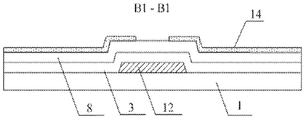
도 4는 도 2의 B1-B1선의 단면도이다.
도 5는 본 발명의 실시예에 관한 TFT-LCD 어레이 기판의 첫번째 패터닝후의 평면도이다.
도 6은 도 5의 A2-A2선의 단면도이다.
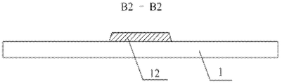
도 7은 도 5의 B2-B2선의 단면도이다.
도 8은 본 발명의 실시예에 관한 TFT-LCD 어레이 기판의 2번째 패터닝후의 평면도이다.
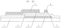
도 9는 도 8의 A3-A3선의 단면도이다.
도 10은 도 8의 B3-B3선의 단면도이다.
도 11은 본 발명의 실시예에 관한 TFT-LCD 어레이 기판의 3번째 패터닝후의 평면도이다.
도 12는 도 11의 A4-A4선의 단면도이다.
도 13은 도 11의 B4-B4선의 단면도이다.1 is a schematic diagram showing a planar structure of a conventional TFT-LCD array substrate.
2 is a schematic diagram showing a planar structure of a TFT-LCD array substrate according to an embodiment of the present invention.
3 is a cross-sectional view taken along a line A1-A1 of FIG. 2.
4 is a cross-sectional view taken along line B1-B1 of FIG. 2.
5 is a plan view after the first patterning of the TFT-LCD array substrate according to the embodiment of the present invention.
6 is a cross-sectional view taken along the line A2-A2 of FIG. 5.
FIG. 7 is a cross-sectional view taken along line B2-B2 of FIG. 5.
8 is a plan view after the second patterning of the TFT-LCD array substrate according to the embodiment of the present invention.
9 is a cross-sectional view taken along the line A3-A3 in FIG. 8.
10 is a cross-sectional view taken along the line B3-B3 in FIG. 8.
11 is a plan view after third patterning of the TFT-LCD array substrate according to the embodiment of the present invention.
12 is a cross-sectional view taken along the line A4-A4 of FIG. 11.
It is sectional drawing of the B4-B4 line of FIG.
이하, 도면과 실시예에 기초하여 본 발명의 기술안에 관하여 더욱 상세히 설명하기로 한다.Hereinafter, the technical solution of the present invention will be described in detail with reference to the drawings and embodiments.
도 2는 본 발명의 실시예에 관한 TFT-LCD 어레이 기판의 평면 구조를 도시한 개략도로서, 상하 인접한 2개의 화소 영역의 구조가 도시되었다. 도 3은 도 2의 A1-A1선의 단면도이고, 도 4는 도 2의 B1-B1선의 단면도이다.Fig. 2 is a schematic diagram showing a planar structure of a TFT-LCD array substrate according to an embodiment of the present invention, in which the structure of two vertically adjacent pixel regions is shown. 3 is a cross-sectional view taken along the line A1-A1 of FIG. 2, and FIG. 4 is a cross-sectional view taken along the line B1-B1 of FIG. 2.
도 2 내지 도 4에 도시한 것처럼, 본 발명의 실시예에 관한 TFT-LCD 어레이 기판에는 기판으로 형성된 여러 개의 게이트 라인(11), 여러 개의 데이터 라인(13) 및 여러 개의 공통 전극 라인(12)이 포함된다. 게이트 라인(11)과 데이터 라인(13)이 서로 교차되어 구분된 여러 개의 화소 영역에 화소 전극(14)과 박막 트랜지스터가 형성된다. 상하 인접한 2개의 화소 영역은 공통 전극 라인(12)을 공유한다. 게이트 라인(11)은 박막 트랜지스터에 온 신호를 제공하기 위해 사용되고, 데이터 라인(13)은 화소 전극(14)에 데이터 신호를 제공하기 위해 사용된다.2 to 4, the TFT-LCD array substrate according to the embodiment of the present invention includes
상하 인접한 2개의 화소 영역이 공통 전극 라인(12)을 공용하는 상황에는 이하의 것이 포함된다. 즉,The following are included in the situation where two vertically adjacent pixel areas share the
상하 인접한 2개의 화소 영역에서 윗쪽 화소 영역의 게이트 라인(11)은 해당 화소 영역의 윗쪽에 위치하고, 아래쪽 화소 영역의 게이트 라인(11)은 해당 화소 영역의 아래쪽에 위치하고, 또한 윗쪽 화소 영역의 윗쪽에 위치하는 게이트 라인(11)과 아래쪽 화소 영역의 아래쪽에 위치하는 게이트 라인(11) 사이에 화소 전극(14)과 축적 용량을 형성함과 동시에 2개의 화소 영역에 공유되는 공통 전극 라인(12)이 설치된다. 즉, 2개의 화소 전극(14)을 끼운 2개의 게이트 라인(11) 사이에 공통 전극 라인(12)이 마련된다. 해당 가로로 연장된 공통 전극 라인(12)은 상하 인접한 2개의 화소 영역의 화소 전극(14)과 축적 용량을 구성하는 한편, 화소 영역의 양측에 입설된 제1 차광 바(15)와 제2 차광 바(16)에 접속하여 차광 구조를 구성하기 위해 사용된다.In two up and down adjacent pixel areas, the
여기에서 박막 트랜지스터에는 게이트 전극(2), 게이트 절연층(3), 반도체층(4), 도핑 반도체층(5), 소스 전극(6), 드레인 전극(7) 및 패시베이션층(8)이 포함된다. 게이트 전극(2)은 기판(1)에 형성됨과 동시에 게이트 라인(11)과 접속한다. 게이트 절연층(3)은 게이트 전극(2)과 게이트 라인(11) 위에 형성됨과 동시에 기판(1) 전체를 덮고, 반도체층(4)과 도핑 반도체층(5)이 적층되어 형성되는 활성층 랜드는 게이트 절연층(3)에 형성됨과 동시에 게이트 전극(2)의 윗쪽에 위치한다. 소스 전극(6)과 드레인 전극(7)은 활성층 랜드에 형성한다. 소스 전극(6)의 일단은 게이트 전극(2)의 윗쪽에 위치함과 동시에 타단은 데이터 라인(13)과 접속하고, 드레인 전극(7)의 일단은 게이트 전극(2)의 윗쪽에 위치함과 동시에 타단은 패시베이션층(8)에 뚫은 패시베이션층 비아홀(9)을 통해 화소 전극(14)과 접속한다. 소스 전극(6)과 드레인 전극(7) 사이에 TFT채널 영역을 형성하여 TFT채널 영역에서의 반도체층(4)이 노출되도록 TFT채널 영역에서의 도핑 반도체를 완전히 식각함과 동시에 반도체층의 두께의 일부도 식각한다. 패시베이션층(8)은 데이터 라인(13), 소스 전극(6) 및 드레인 전극(7) 위에 형성됨과 동시에 기판(1)의 전체를 덮는다. 또 패시베이션층(8)에서 드레인 전극(7)이 존재하는 위치에 드레인 전극(7)과 화소 전극(14)을 접속하기 위한 패시베이션층 비아홀(9)을 뚫는다. 상하 인접한 2개의 화소 영역을 1조로 하면, 공통 전극 라인(12)은 상하 인접한 2개의 화소 영역의 게이트 라인(11)과 게이트 라인(11) 사이에 위치함과 동시에 상하 인접한 2개의 화소 영역의 게이트 라인(11)과 평행하고, 제1 차광 바(15)와 제2 차광 바(16)는 데이터 라인(13)과 평행하고, 제1 차광 바(15)는 화소 영역의 왼쪽에 위치함과 동시에 화소 영역의 왼쪽의 데이터 라인(13)에 접근한다. 제2 차광 바(16)는 화소 영역의 오른쪽에 위치함과 동시에 화소 영역의 오른쪽의 데이터 라인(13)에 접근한다. 공통 전극 라인(12)은 제1 차광 바(15)와 제2 차광 바(16)의 각각에 접속하여 일체 구조가 된 공통 전극 라인(12), 제1 차광 바(15)와 제2 차광 바(16)는 각각의 화소 영역과 함께 윗쪽으로 오목형 또는 아래쪽으로 오목형이 되는 차광 구조를 구성한다. 또 화소 전극(14)과 공통 전극 라인(12)에 의해 축적 용량이 공통 전극 라인상(Cst on Common)에서의 구조가 형성되도록 화소 전극(14)과 공통 전극 라인(12)이 오버랩된다.The thin film transistor includes a gate electrode 2, a
본 발명의 실시예에서 종래의 상하 인접한 2개의 화소 영역의 2개의 공통 전극 라인(12)이 하나의 공통 전극 라인(12)으로 줄어들도록 상하 인접한 2개의 화소 영역이 하나의 공통 전극 라인(12)을 공유한다. 공통 전극 라인(12)은 금속 재료로 이루어지고 투광성이 없기 때문에 하나의 공통 전극 라인(12)을 줄이면 화소 영역의 투광성이 향상된다. 따라서 표시 성능에 영향을 받지 않으면서 효율적으로 개구율을 향상시키고 표시 휘도가 변하지 않는 상태에서 백라이트의 에너지 손실도 효과적으로 줄어든다.In the exemplary embodiment of the present invention, the two
도 5 내지 도 13은 본 발명의 실시예에 관한 TFT-LCD 어레이 기판의 제조 과정의 개략도이며, 나아가 본 발명의 실시예에 관한 기술안에 대해 설명하기로 한다. 이하의 설명에서 이른바 패터닝에는, 포토레지스트 도포, 마스킹, 포토레지스트에 대한 노광과 현상, 포토레지스트의 패턴을 이용하는 식각 및 포토레지스트의 박리 등의 프로세스가 포함되며 포토레지스트는 포지티브 포토레지스트를 예로 한다.5 to 13 are schematic diagrams of the manufacturing process of the TFT-LCD array substrate according to the embodiment of the present invention, and further description will be given on the technical proposal of the embodiment of the present invention. In the following description, so-called patterning includes processes such as photoresist application, masking, exposure and development to photoresist, etching using patterns of photoresist and peeling of photoresist, and the photoresist taking positive photoresist as an example.
도 5는 본 발명의 실시예에 관한 TFT-LCD 어레이 기판의 첫번째 패터닝 후의 평면도로서, 상하 인접한 2개의 화소 영역의 구조가 도시되었다. 도 6은 도 5의 A2-A2선의 단면도이고, 도 7은 도 5의 B2-B2선의 단면도이다.Fig. 5 is a plan view after the first patterning of the TFT-LCD array substrate according to the embodiment of the present invention, in which the structure of two vertically adjacent pixel regions is shown. 6 is a cross-sectional view taken along the line A2-A2 of FIG. 5, and FIG. 7 is a cross-sectional view taken along the line B2-B2 of FIG. 5.
우선, 스퍼터링 또는 증착법을 이용하여 기판(1)(예를 들면, 유리 기판 또는 석영 기판)에 1층의 게이트 금속 박막을 퇴적하고 해당 게이트 금속 박막으로서 Mo,Al 등의 금속 단층막이 채용되어도 좋고, 복층 금속 박막으로 이루어진 복합 박막(예를 들면, Mo/Al/Mo복합 박막)이 채용되어도 좋다. 또 도 5 내지 도 7에 도시된 것처럼, 통상의 마스크를 채용하여 게이트 금속 박막에 대해 패터닝함으로써 기판(1)에 각각의 화소 영역에서의 게이트 라인(11), 게이트 전극(2), 공통 전극 라인(12), 제1 차광 바(15) 및 제2 차광 바(16)를 형성한다. 공통 전극 라인(12)은 상하 인접한 2개의 화소 영역의 게이트 라인(11)과 게이트 라인(11) 사이에 위치함과 동시에 상하 인접한 2개의 화소 영역의 게이트 라인(11)과 평행하다. 제1 차광 바(15)와 제2 차광 바(16)는 나중에 형성되는 데이터 라인(13)과 평행하다. 제1 차광 바(15)는 화소 영역의 왼쪽에 위치함과 동시에 화소 영역의 왼쪽의 데이터 라인(13)에 접근하고, 제2 차광 바(16)는 화소 영역의 오른쪽에 위치함과 동시에 화소 영역의 오른쪽의 데이터 라인(13)에 접근한다. 공통 전극 라인(12)은 제1 차광 바(15)와 제2 차광 바(16)의 각각에 접속하여 일체 구조가 된 공통 전극 라인(12), 제1 차광 바(15)와 제2 차광 바(16)는 각각의 화소 영역과 함께 윗쪽이 오목형 또는 아래쪽이 오목형인 차광 구조를 구성한다. 즉, 상하 인접한 2개의 화소 영역이 공통 전극 라인(12)을 공유한다.First, one layer of gate metal thin film may be deposited on the substrate 1 (for example, a glass substrate or a quartz substrate) by sputtering or vapor deposition, and a metal single layer film such as Mo or Al may be employed as the gate metal thin film. A composite thin film (for example, Mo / Al / Mo composite thin film) composed of a multilayer metal thin film may be employed. 5 to 7, the
도 8은 본 발명의 실시예에 관한 TFT-LCD 어레이 기판의 2번째 패터닝 후의 평면도로서, 상하 인접한 2개의 화소 영역의 구조가 도시되었다. 도 9는 도 8의 A3-A3선의 단면도이고, 도 10은 도 8의 B3-B3선의 단면도이다.Fig. 8 is a plan view after the second patterning of the TFT-LCD array substrate according to the embodiment of the present invention, in which the structure of two vertically adjacent pixel regions is shown. FIG. 9 is a cross-sectional view taken along the line A3-A3 of FIG. 8, and FIG. 10 is a cross-sectional view taken along the line B3-B3 of FIG. 8.
상기 구조를 완성한 기판에 우선 플라즈마 강화 화학적 기상 증착법(이하 PECVD로 약칭한다)을 이용하여 게이트 절연층, 반도체 박막 및 도핑 반도체 박막을 차례대로 퇴적한 후에 스퍼터링 또는 증착법을 이용하여 1층의 소스·드레인 금속 박막을 퇴적한다. 게이트 절연박막으로서 산화물, 질화물 또는 질산화물이 채용되고 소스·드레인 금속 박막으로서 Mo,Al 등의 금속 단층막, 또는 Cu 등 저항율이 낮은 금속 단층막이 채용되어도 좋고, 복층 금속 박막으로 이루어진 복합 박막(예를 들면, Mo/Al/Mo복합 박막)이 채용되어도 좋다. 도 8 내지 도 10에 도시된 것처럼 하프톤 또는 그레이톤의 마스크를 채용하고 패터닝에 의해 각각의 화소 영역에서의 데이터 라인(13), 소스 전극(6), 드레인 전극(7) 및 TFT채널 영역을 형성한다. 해당 2번째 패터닝은 멀티 단계의 식각이어도 좋다. 그 프로세스에는 예를 들면 이하의 공정이 포함된다. 즉, 우선 소스·드레인 금속 박막에 1층의 포토레지스트를 도포하고 하프톤 또는 그레이톤의 마스크를 채용하여 포토레지스트에 대해 노광을 하여 포토레지스트에 완전 노광 영역, 비노광영역 및 반절 노광 영역을 형성한다. 그 중, 비노광영역은 데이터 라인(13), 소스 전극(6) 및 드레인 전극(7)이 존재하는 영역에 대응하고, 반절 노광 영역은 소스 전극(6)과 드레인 전극(7)간의 TFT채널 영역이 존재하는 영역에 대응하고, 완전 노광 영역은 남겨진 영역에 대응한다. 노광된 포토레지스트에 대해 현상 처리한 후, 비노광영역의 포토레지스트의 두께에 변화가 없어 포토레지스트 완전 보류 영역이 형성되고, 완전 노광 영역의 포토레지스트가 완전히 제거되어 포토레지스트 완전 제거 영역이 형성되고, 반절 노광 영역의 포토레지스트의 두께가 얇아져 포토레지스트 반절 보류 영역이 형성된다. 첫번째 식각을 이용하여 완전 노광 영역의 소스·드레인 금속 박막, 도핑 반도체 박막 및 반도체 박막을 완전히 식각함으로써 데이터 라인(13), 소스 전극(6) 및 드레인 전극(7)을 형성한다. 애싱을 이용하여 반절 노광 영역의 포토레지스트를 제거함으로써 해당 영역의 소스·드레인 금속 박막을 노출시킨다. 2번째 식각을 이용하여 반절 노광 영역의 소스·드레인 금속 박막 및 도핑 반도체 박막을 완전히 식각함과 동시에 반도체 박막의 두께 일부를 식각함으로써 반도체 박막이 노출되어 소스 전극(6), 드레인 전극(7) 및 TFT채널 영역이 형성된다. 마지막으로 남겨진 포토레지스트를 벗겨 본 실시예의 TFT-LCD 어레이 기판의 2번째 패터닝을 완성한다. 이 패터닝을 한 후, 게이트 절연층(3)은 기판(1) 전체를 덮고 반도체층(4)과 도핑 반도체층(5)에 의해 구성된 활성층 랜드가 게이트 절연층(3)에 형성됨과 동시에 게이트 전극(2)의 윗쪽에 위치한다. 소스 전극(6)과 드레인 전극(7)은 활성층 랜드에 형성되고, 소스 전극(6)의 일단은 게이트 전극(2)의 윗쪽에 위치함과 동시에 다른 일단은 데이터 라인(13)과 접속한다. 드레인 전극(7)의 일단은 게이트 전극(2)의 윗쪽에 위치함과 동시에 소스 전극(6)에 대향하여 배치된다. 또 소스 전극(6)과 드레인 전극(7) 사이에 TFT채널 영역이 형성된다. 또 TFT채널 영역의 반도체 박막이 노출되도록 TFT채널 영역에서의 도핑 반도체 박막을 완전히 식각함과 동시에 반도체 박막의 두께 일부도 식각한다. 게이트 라인(11)과 데이터 라인(13)이 화소 영역을 구분한다. 데이터 라인(13)은 제1 차광 바(15) 또는 제2 차광 바(16)의 바깥쪽에 위치하고 데이터 라인(13)의 아래쪽에 도핑 반도체 박막 및 반도체 박막이 보류된다.The gate insulating layer, the semiconductor thin film, and the doped semiconductor thin film are sequentially deposited on the substrate having the above structure by using plasma enhanced chemical vapor deposition (hereinafter abbreviated as PECVD), and then the source and drain of one layer by sputtering or vapor deposition. A metal thin film is deposited. Oxide, nitride, or nitrate may be employed as the gate insulating thin film, and a metal single layer film such as Mo or Al, or a metal single layer film having a low resistivity such as Cu may be employed as the source / drain metal thin film. For example, Mo / Al / Mo composite thin film) may be employed. As shown in Figs. 8 to 10, a mask of halftone or graytone is employed and patterning is performed to pattern the
도 11은 본 발명의 실시예에 관한 TFT-LCD 어레이 기판의 3번째 패터닝후의 평면도로서, 상하 인접한 2개의 화소 영역의 구조가 도시되었다. 도 12는 도 11의 A4-A4선의 단면도이고, 도 13은 도 11의 B4-B4선의 단면도이다.Fig. 11 is a plan view after the third patterning of the TFT-LCD array substrate according to the embodiment of the present invention, and the structure of two pixel regions adjacent up and down is shown. FIG. 12 is a cross-sectional view taken along the line A4-A4 of FIG. 11, and FIG. 13 is a cross-sectional view taken along the line B4-B4 of FIG. 11.
도 11 내지 도 13에 도시한 것처럼, 상기 구조를 완성한 기판에 플라즈마 강화 화학적 기상 증착법(PECVD)을 이용하여 1층의 패시베이션층(8)을 퇴적한다. 패시베이션층(8)으로서 산화물, 질화물 또는 질산화물이 채용된다. 통상의 마스크를 채용하여 패시베이션층에 대해 패터닝함으로써 패시베이션층에 패시베이션층 비아홀(9)이 형성된다. 해패시베이션층 비아홀(9)은 드레인 전극(7)의 윗쪽에 위치한다. 이 패터닝에서, 게이트 라인 패드(게이트 라인 패드) 영역의 게이트 라인 패드 비아홀 및 데이터 라인 패드(데이터 라인 패드) 영역의 데이터 라인 패드 비아홀 등이 동시에 형성된다.As shown in Figs. 11 to 13, one passivation layer 8 is deposited on the substrate having the above structure by using plasma enhanced chemical vapor deposition (PECVD). As the passivation layer 8, oxides, nitrides or nitrides are employed. The passivation layer via hole 9 is formed in the passivation layer by patterning the passivation layer by employing a normal mask. The passivation layer via hole 9 is located above the
마지막으로 상기 구조를 완성한 기판에 스퍼터링법이나 증착법을 이용하여 투명 도전 박막을 퇴적하고, 투명 도전 박막으로서 산화 인듐 주석(ITO), 산화 인듐 아연(IZO), 또는, 산화 알루미늄아연 등의 재료가 채용된다. 다른 투명 금속 또는 투명 금속 산화물이 채용되어도 좋다. 통상의 마스크를 채용하여 패터닝에 의해 화소 전극(14)을 형성한다. 화소 전극(14)은 각각의 화소 영역내에 형성되고 패시베이션층 비아홀(9)을 통해 드레인 전극(7)과 접속한다. 또 상하 인접한 2개의 화소 영역 사이에서 화소 전극(14)과 공통 전극선(12)에 의해 축적 용량이 공통 전극 라인상(Cst on Common)에서의 구조가 형성되도록 화소 전극(14)은 공통 전극 라인(12)을 덮는다.Finally, a transparent conductive thin film is deposited on a substrate having the above structure by sputtering or vapor deposition, and a material such as indium tin oxide (ITO), indium zinc oxide (IZO), or aluminum zinc oxide is employed as the transparent conductive thin film. do. Other transparent metals or transparent metal oxides may be employed. The
이상에서 설명한 4회의 패터닝은 본 발명에 관한 TFT-LCD 어레이 기판을 제조하는 일종의 실현 방법에 불과하다. 실제로는 패터닝 횟수를 늘리거나 줄일 수 있다. 또 다른 재료를 선택하거나 또는 재료를 조합함으로써 본 발명을 실현할 수도 있다. 예를 들면, 본 발명에 관한 TFT-LCD 어레이 기판의 2번째 패터닝은, 2회의 통상의 마스크에 의한 패터닝에 의해 완성해도 좋다. 즉, 1회는 통상의 마스크를 채용하는 패터닝에 의해 활성층 랜드를 형성하고, 1회는 통상의 마스크를 채용하는 패터닝에 의해 데이터 라인, 소스 전극, 드레인 전극 및 TFT채널 영역을 형성한다. 이 예시에서, 구체적으로 우선 PECVD법을 이용하여 게이트 절연 박막, 반도체 박막 및 도핑 반도체 박막을 차례대로 퇴적한 후 통상의 마스크를 채용하는 패터닝에 의해 활성층 랜드를 형성한다. 해당 활성층은 반도체층과 도핑 반도체층의 적층체를 포함하여 게이트 절연층에 형성됨과 동시에 게이트 전극의 윗쪽에 위치한다. 다음으로 스퍼터링 또는 증착법을 이용하여 1층의 소스·드레인 금속 박막을 퇴적한다. 다음으로 통상의 마스크를 채용하는 패터닝에 의해 데이터 라인, 소스 전극, 드레인 전극 및 TFT채널 영역을 형성한다. 소스 전극의 일단은 활성층 랜드에 위치함과 동시에 타단은 데이터 라인과 접속한다. 또 드레인 전극의 일단은 활성층 랜드에 위치함과 동시에 소스 전극에 대향하여 배치되고 소스 전극과 드레인 전극 사이에 TFT채널 영역을 형성하여 TFT채널 영역의 반도체층이 노출되도록 TFT채널 영역에서의 도핑 반도체 박막을 완전히 식각함과 동시에 반도체 박막의 두께 일부를 식각한다. 이 패터닝을 한 후, 데이터 라인의 아래쪽에 게이트 절연층밖에 존재하지 않는다.The four-time patterning described above is merely a kind of realization method of manufacturing the TFT-LCD array substrate according to the present invention. In practice, you can increase or decrease the number of patterns. The present invention may be realized by selecting another material or combining materials. For example, the second patterning of the TFT-LCD array substrate according to the present invention may be completed by patterning with two normal masks. That is, the active layer land is formed by patterning employing a conventional mask once, and the data line, source electrode, drain electrode and TFT channel region are formed by patterning employing a conventional mask once. In this example, specifically, first, the gate insulating thin film, the semiconductor thin film, and the doped semiconductor thin film are sequentially deposited by PECVD, and then the active layer land is formed by patterning using a conventional mask. The active layer is formed on the gate insulating layer including the laminate of the semiconductor layer and the doped semiconductor layer and is located above the gate electrode. Next, one source / drain metal thin film is deposited by sputtering or vapor deposition. Next, a data line, a source electrode, a drain electrode, and a TFT channel region are formed by patterning employing a normal mask. One end of the source electrode is located in the active layer land and the other end is connected to the data line. One end of the drain electrode is disposed in the active layer land and is disposed opposite the source electrode, and forms a TFT channel region between the source electrode and the drain electrode to expose the semiconductor layer of the TFT channel region so that the semiconductor layer of the TFT channel region is exposed. While etching completely, a portion of the thickness of the semiconductor thin film is etched. After this patterning, only the gate insulating layer exists below the data line.
또 상기 실시예에서 박막 트랜지스터가 상하 인접한 2개의 화소 영역의 같은 쪽에 위치하는 것만을 예로 들어 설명하였으나, 당업자라면 박막 트랜지스터가 상하 인접한 2개의 화소 영역의 양측에도 위치할 수 있어 그 실현 원리는 같다는 것을 이해할 수 있기 때문에 설명을 생략한다.In the above embodiment, only the thin film transistors are positioned on the same side of two pixel regions vertically adjacent to each other. However, those skilled in the art will realize that the thin film transistors may be located on both sides of the two pixel regions vertically adjacent to each other. The description is omitted because it can be understood.
아울러 본 발명의 실시예에 관한 TFT-LCD 어레이 기판은 상하 인접한 2개의 화소 영역이 공통 전극 라인을 공유하는 구조를 채용하여 표시 품질에 영향이 없다는 전제로 화소 개구율을 효과적으로 향상시키는 기술안이다. 종래와 같은 각각의 화소 영역에 하나의 공통 전극 라인을 배치하는 구조를 채용하는 경우에 비해 본 발명의 실시예에 의해 제공된 TFT-LCD 어레이 기판은 상하 인접한 2개의 화소 영역에서 하나의 공통 전극 라인을 생략할 수 있어 화소 영역의 개구율을 효과적으로 향상시킴과 동시에 표시 휘도가 변하지 않는 상황에서 백라이트의 에너지 손실도 효과적으로 줄일 수 있게 됨에 따라 TFT-LCD 어레이 기판의 생산 비용를 줄였다. 또 본 발명의 실시예에서 TFT-LCD 어레이 기판을 제조하는 경우 역시 4회의 패터닝 또는 5회의 패터닝을 채용할 수 있고 패터닝을 늘리지 않은 상태에서 전체적으로 TFT-LCD의 성능과 품질을 향상시켰다.In addition, the TFT-LCD array substrate according to the embodiment of the present invention is a technique for effectively improving the pixel aperture ratio on the premise that the display quality is not affected by adopting a structure in which two upper and lower adjacent pixel regions share a common electrode line. Compared to the case of employing a structure in which one common electrode line is disposed in each pixel region as in the related art, the TFT-LCD array substrate provided by the embodiment of the present invention is one common electrode line in two adjacent pixel regions. Since it can be omitted, the aperture ratio of the pixel area can be effectively improved, and the energy loss of the backlight can be effectively reduced while the display brightness does not change, thereby reducing the production cost of the TFT-LCD array substrate. In the embodiment of the present invention, when manufacturing a TFT-LCD array substrate, four patterning or five patterning may also be employed, and the overall performance and quality of the TFT-LCD may be improved without increasing the patterning.
본 발명의 실시예에서의 TFT-LCD 어레이 기판의 제조 방법에는 이하의 단계를 포함시킬 수 있다. 즉,The manufacturing method of the TFT-LCD array substrate in the embodiment of the present invention may include the following steps. In other words,
단계1: 기판에 게이트 금속 박막을 퇴적하여 상기 게이트 금속 박막에 대해 패터닝함으로써 각각의 화소 영역에서의 게이트 라인, 게이트 전극 및 공통 전극 라인을 형성하여 상하 인접한 2개의 화소 영역에 공통 전극 라인을 공유시킨다.Step 1: By depositing a gate metal thin film on a substrate and patterning the gate metal thin film, a gate line, a gate electrode, and a common electrode line in each pixel area are formed to share a common electrode line in two vertically adjacent pixel areas. .
단계2: 단계1을 완성한 기판에 게이트 절연층, 반도체 박막, 도핑 반도체 박막 및 소스·드레인 금속 박막을 퇴적하고 상기 게이트 절연층, 반도체 박막, 도핑 반도체 박막 및 소스·드레인 금속 박막에 대해 패터닝함으로써 각각의 화소 영역에서의 활성층 랜드, 데이터 라인, 드레인 전극, 소스 전극 및 TFT채널을 형성한다.Step 2: A gate insulating layer, a semiconductor thin film, a doped semiconductor thin film and a source / drain metal thin film are deposited on the substrate having completed Step 1 and patterned for the gate insulating layer, the semiconductor thin film, the doped semiconductor thin film and the source / drain metal thin film, respectively. An active layer land, a data line, a drain electrode, a source electrode and a TFT channel are formed in the pixel region of the film.
단계3: 단계2를 완성한 기판에 패시베이션층을 퇴적하고 상기 패시베이션층에 대해 패터닝함으로써 드레인 전극의 윗쪽에 위치하는 패시베이션층 비아홀을 형성한다.Step 3: A passivation layer is deposited on the substrate having completed step 2 and patterned with respect to the passivation layer to form a passivation layer via hole located above the drain electrode.
단계4: 단계3을 완성한 기판에 투명 도전 박막을 퇴적하고 상기 투명 도전 박막에 대해 패터닝함으로써 각각의 화소 영역에서의 화소 전극을 형성하고 상기 화소 전극은 패시베이션층 비아홀을 통해 드레인 전극과 접속된다.Step 4: A transparent conductive thin film is deposited on the substrate having completed
본 발명의 실시예에 관한 TFT-LCD 어레이 기판의 제조 방법에서, 상하 인접한 2개의 화소 영역이 공통 전극 라인을 공유하는 구조를 형성함으로써 표시 품질에 영향이 없는 상황에서 개구율을 효과적으로 향상시켰다. 종래와 같은 각각의 화소 영역에 하나의 공통 전극 라인을 배치하는 구조를 채용하는 경우에 비해 본 발명의 실시예에 의해 제공된 TFT-LCD 어레이 기판은 상하 인접한 2개의 화소 영역에서 하나의 공통 전극 라인을 생략할 수 있어 화소 영역의 개구율을 효과적으로 향상시킴과 동시에 표시 휘도가 변하지 않는 상황에서 백라이트의 에너지 손실도 효과적으로 줄임에 따라 TFT-LCD 어레이 기판의 생산 비용을 줄였다. 또 본 발명의 실시예에서 TFT-LCD 어레이 기판을 제조하는 경우 역시 4회의 패터닝 또는 5회의 패터닝을 채용할 수 있고 패터닝을 늘리지 않은 상태에서 전체적으로 TFT-LCD의 성능과 품질을 향상시켰다.In the method of manufacturing a TFT-LCD array substrate according to the embodiment of the present invention, the aperture ratio is effectively improved in a situation where display quality is not affected by forming a structure in which two upper and lower adjacent pixel regions share a common electrode line. Compared to the case of employing a structure in which one common electrode line is disposed in each pixel region as in the related art, the TFT-LCD array substrate provided by the embodiment of the present invention is one common electrode line in two adjacent pixel regions. Since it can be omitted, the aperture ratio of the pixel area can be effectively improved, and the energy loss of the backlight is effectively reduced while the display brightness does not change, thereby reducing the production cost of the TFT-LCD array substrate. In the embodiment of the present invention, when manufacturing a TFT-LCD array substrate, four patterning or five patterning may also be employed, and the overall performance and quality of the TFT-LCD may be improved without increasing the patterning.
또 단계1에서 공통 전극 라인과 접속하는 제1 차광 바와 제2 차광 바도 형성할 수 있다. 제1 차광 바와 제2 차광 바는 데이터 라인과 평행함과 동시에 상하 인접한 2개의 화소 영역의 양측에 위치한다. 우선 스퍼터링 또는 증착법을 이용하여 기판(예를 들면 유리 기판 또는 석영 기판)에 1층의 게이트 금속 박막을 퇴적한다. 해당 게이트 금속 박막으로서 Mo, Al 등의 금속 단층막이 채용되어도 좋고, 복층 금속 박막으로 이루어진 복합 박막(예를 들면, Mo/Al/Mo복합 박막)이 채용되어도 좋다. 또 통상의 마스크(모노톤 마스크라고도 칭한다)를 채용하여 게이트 금속 박막에 대해 패터닝함으로써 기판에 게이트 라인, 게이트 전극, 공통 전극 라인, 제1 차광 바 및 제2 차광 바를 형성한다. 공통 전극 라인은 상하 인접한 2개의 화소 영역의 게이트 라인과 게이트 라인 사이에 위치함과 동시에 상하 인접한 2개의 화소 영역의 게이트 라인과 평행하다. 또 제1 차광 바와 제2 차광 바는 데이터 라인과 평행하고 제1 차광 바는 화소 영역의 왼쪽에 위치함과 동시에 화소 영역의 왼쪽의 데이터 라인에 접근하고, 제2 차광 바는 화소 영역의 오른쪽에 위치함과 동시에 화소 영역의 오른쪽의 데이터 라인에 접근한다. 또 공통 전극 라인은 제1 차광 바와 제2 차광 바의 각각과 접속하여 일체 구조가 된 공통 전극 라인, 제1 차광 바와 제2 차광 바는 각각의 화소 영역과 함께 윗쪽이 오목형 또는 아래쪽이 오목형인 차광 구조를 구성한다. 즉, 상하 인접한 2개의 화소 영역이 공통 전극 라인을 공유한다.In addition, a first light blocking bar and a second light blocking bar connected to the common electrode line in step 1 may be formed. The first light blocking bar and the second light blocking bar are positioned at both sides of two pixel areas parallel to and parallel to the data line. First, a gate metal thin film of one layer is deposited on a substrate (for example, a glass substrate or a quartz substrate) by sputtering or vapor deposition. As the gate metal thin film, a metal single layer film such as Mo or Al may be employed, or a composite thin film made of a multilayer metal thin film (for example, a Mo / Al / Mo composite thin film) may be employed. A gate mask, a gate electrode, a common electrode line, a first light blocking bar, and a second light blocking bar are formed on the substrate by patterning the gate metal thin film using a normal mask (also called a monotone mask). The common electrode line is positioned between the gate line and the gate line of two vertically adjacent pixel regions and is parallel to the gate line of the two vertically adjacent pixel regions. In addition, the first light blocking bar and the second light blocking bar are parallel to the data line, and the first light blocking bar is located on the left side of the pixel area and approaches the data line on the left side of the pixel area, and the second light blocking bar is located on the right side of the pixel area. At the same time, the data line on the right side of the pixel area is accessed. The common electrode line may be connected to each of the first light blocking bar and the second light blocking bar to form an integrated structure, and the first light blocking bar and the second light blocking bar may be concave at the top or concave at the bottom together with the respective pixel areas. It constitutes a light shielding structure. That is, two vertically adjacent pixel regions share a common electrode line.
본 실시예의 TFT-LCD 어레이 기판의 제조 방법의 제1 예시에서, 상기 단계2에는 이하의 단계가 포함된다. 즉,In the first example of the method of manufacturing the TFT-LCD array substrate of the present embodiment, the above step 2 includes the following steps. In other words,
단계11: 단계1을 완성한 기판에 플라즈마 강화 화학적 기상 증착법을 이용하여 게이트 절연층, 반도체 박막 및 도핑 반도체 박막을 차례대로 퇴적한다.Step 11: A gate insulating layer, a semiconductor thin film, and a doped semiconductor thin film are sequentially deposited on the substrate having completed Step 1 by using plasma enhanced chemical vapor deposition.
단계12: 단계11을 완성한 기판에 스퍼터링 또는 증착법을 이용하여 소스·드레인 금속 박막을 퇴적한다.Step 12: A source / drain metal thin film is deposited on the substrate having completed
단계13: 소스·드레인 금속 박막에 1층의 포토레지스트를 도포한다.Step 13: Apply one layer of photoresist on the source / drain metal thin film.
단계14: 하프톤 또는 그레이톤의 마스크를 이용하여 노광함으로써 포토레지스트를 포토레지스트 완전 보류 영역, 포토레지스트 완전 제거 영역 및 포토레지스트 반절 보류 영역에 형성시킨다. 포토레지스트 완전 보류 영역은 데이터 라인, 소스 전극 및 드레인 전극이 존재하는 영역에 대응하고 포토레지스트 반절 보류 영역은 소스 전극과 드레인 전극간의 TFT채널 영역이 존재하는 영역에 대응하고, 포토레지스트 완전 제거 영역은 남겨진 영역에 대응한다. 현상 처리한 후, 포토레지스트 완전 보류 영역의 포토레지스트의 두께에 변화가 없어 포토레지스트 완전 제거 영역의 포토레지스트가 완전히 제거되고 포토레지스트 반절 보류 영역의 포토레지스트의 두께가 얇아진다.Step 14: The photoresist is formed in the photoresist full retention region, the photoresist complete removal region and the photoresist half retention region by exposing with a mask of halftone or graytone. The photoresist complete retention region corresponds to the region where the data line, the source electrode and the drain electrode exist, and the photoresist half retention region corresponds to the region where the TFT channel region between the source electrode and the drain electrode exists, and the photoresist complete removal region is Corresponds to the remaining area. After the development treatment, there is no change in the thickness of the photoresist in the photoresist complete retention region so that the photoresist in the photoresist complete removal region is completely removed and the thickness of the photoresist in the photoresist half retention region becomes thin.
단계15: 첫번째 식각에 의해 포토레지스트 완전 제거 영역의 소스·드레인 금속 박막, 도핑 반도체 박막 및 반도체 박막을 완전히 식각하여 활성층 랜드와 데이터 라인을 형성한다.Step 15: The first etching completely removes the source / drain metal thin film, the doped semiconductor thin film and the semiconductor thin film in the photoresist removal region to form an active layer land and a data line.
단계16: 애싱을 이용하여 포토레지스트 반절 보류 영역의 포토레지스트를 제거함으로써 해당 영역의 소스·드레인 금속 박막을 노출시킨다.Step 16: Expose the photoresist thin film of the region by removing the photoresist in the photoresist half-retention region using ashing.
단계17: 2번째의 식각을 이용하여 포토레지스트 반절 보류 영역의 소스·드레인 금속 박막 및 도핑 반도체 박막을 완전히 식각함과 동시에 반도체 박막의 두께 일부를 식각함으로써 해당 영역의 반도체 박막이 노출되어 소스 전극, 드레인 전극 및 TFT채널 영역을 형성한다.Step 17: using the second etching, the source and drain metal thin films and the doped semiconductor thin film of the photoresist half-retention region are completely etched, and a portion of the thickness of the semiconductor thin film is etched to expose the semiconductor thin film of the corresponding region, thereby exposing the source electrode, A drain electrode and a TFT channel region are formed.
단계18: 남겨진 포토레지스트를 벗긴다.Step 18: Strip off the remaining photoresist.
본 예시에서 하프톤 또는 그레이톤의 마스크를 채용하여 1회 패터닝함으로써 활성층 랜드, 데이터 라인, 소스 전극, 드레인 전극 및 TFT채널 영역을 동시에 형성하는 기술안을 제공하고 상기 단계를 완성하여 형성된 화소 구조를 도 9와 도 10에 도시하였다.In this example, a technique of simultaneously forming an active layer land, a data line, a source electrode, a drain electrode, and a TFT channel region by patterning once using a mask of halftone or gray tone is provided, and the pixel structure formed by completing the above steps is illustrated. 9 and FIG. 10.
본 실시예의 TFT-LCD 어레이 기판의 제조 방법의 제2 예시에서, 상기 단계2에는 이하의 단계가 포함된다. 즉,In a second example of the manufacturing method of the TFT-LCD array substrate of the present embodiment, the above step 2 includes the following steps. In other words,
단계21: 단계1을 완성한 기판에 플라즈마 강화 화학적 기상 증착법을 이용하여 게이트 절연층, 반도체 박막 및 도핑 반도체 박막을 차례대로 퇴적한다.Step 21: A gate insulating layer, a semiconductor thin film and a doped semiconductor thin film are sequentially deposited on the substrate having completed Step 1 by using plasma enhanced chemical vapor deposition.
단계22: 통상의 마스크를 채용하는 패터닝에 의해 활성층 랜드를 형성한다.Step 22: An active layer land is formed by patterning employing a conventional mask.
단계23: 단계22를 완성한 기판에 스퍼터링 또는 증착법을 이용하여 소스·드레인 금속 박막을 퇴적한다.Step 23: A source / drain metal thin film is deposited on the substrate having completed Step 22 by sputtering or vapor deposition.
단계24: 통상의 마스크를 채용하는 패터닝에 의해 데이터 라인, 소스 전극, 드레인 전극 및 TFT채널 영역을 형성한다.Step 24: Form a data line, a source electrode, a drain electrode and a TFT channel region by patterning employing a conventional mask.
본 예시에서 2개의 통상의 마스크를 채용하는 패터닝, 즉 1회는 통상의 마스크를 채용하는 패터닝에 의해 활성층 랜드를 형성하고, 다른 1회는 통상의 마스크를 채용하는 패터닝에 의해 데이터 라인, 소스 전극, 드레인 전극 및 TFT채널 영역을 형성한다.In this example, the active layer land is formed by patterning employing two conventional masks, i.e., patterning employing a conventional mask, and the data line and source electrode by patterning employing a conventional mask. The drain electrode and the TFT channel region are formed.
상기 단계3에서 PECVD법을 이용하여 1층의 패시베이션층을 퇴적할 수 있고 통상의 마스크를 채용하여 패시베이션층에 대해 패터닝함으로써 패시베이션층 비아홀을 형성한다. 이 패시베이션층 비아홀은 드레인 전극의 윗쪽에 위치한다. 상기 단계를 완성하여 형성된 화소 구조를 도 12와 도 13에 도시하였다.In the
단계4에서 스퍼터링법이나 증착법을 이용하여 투명 도전 박막을 퇴적하여 통상의 마스크를 채용하는 패터닝에 의해 화소 전극을 형성하고, 해당 화소 영역내에 화소 전극을 형성함과 동시에 패시베이션층 비아홀을 통해 드레인 전극과 접속시킨다. 상하 인접한 2개의 화소 영역을 1조로 하면, 공통 전극 라인은 상하 인접한 2개의 화소 영역의 게이트 라인과 게이트 라인 사이에 위치함과 동시에 상하 인접한 2개의 화소 영역의 게이트 라인과 평행하고, 제1 차광 바와 제2 차광 바는 데이터 라인과 평행하고, 제1 차광 바는 화소 영역의 왼쪽으로 위치함과 동시에 화소 영역의 왼쪽의 데이터 라인에 접근하고, 제2 차광 바는 화소 영역의 오른쪽에 위치함과 동시에 화소 영역의 오른쪽의 데이터 라인에 접근한다. 또 공통 전극 라인은 제1 차광 바와 제2 차광 바를 접속하여 일체 구조가 된 공통 전극 라인, 제1 차광 바와 제2 차광 바는 각각의 화소 영역과 함께 윗쪽이 오목형 또는 아래쪽이 오목형인 차광 구조를 구성한다. 또 화소 전극과 공통 전극 라인에 의해 축적 용량이 공통 전극 라인(Cst on Common)에서의 구조의 형태가 형성되도록 화소 전극과 공통 전극 라인이 오버랩된다.In step 4, a transparent conductive thin film is deposited using a sputtering method or a vapor deposition method to form a pixel electrode by patterning using a conventional mask, and a pixel electrode in the corresponding pixel region, and at the same time, a drain electrode and a passivation layer via hole are formed. Connect. When the two vertically adjacent pixel regions are one set, the common electrode line is positioned between the gate lines and the gate lines of the two vertically adjacent pixel regions, and is parallel to the gate lines of the two vertically adjacent pixel regions, and the first light blocking bar The second light blocking bar is parallel to the data line, the first light blocking bar is positioned to the left of the pixel area and approaches the data line on the left side of the pixel area, and the second light blocking bar is located to the right of the pixel area Access the data line on the right side of the pixel area. In addition, the common electrode line connects the first light blocking bar and the second light blocking bar to form an integrated structure. The first light blocking bar and the second light blocking bar have a light blocking structure in which a top is concave or a bottom is concave, together with respective pixel regions. Configure. In addition, the pixel electrode and the common electrode line overlap the pixel electrode and the common electrode line so that the storage capacitor has a form of a structure in the common electrode line Cst on Common.
상기 일실시예는 본 발명의 기술안에 관하여 설명했을 뿐이며 이들에 한정되지는 않는다. 구체적 실시예를 참고하면서 본 발명에 관하여 상세하게 설명하였으나, 당업자로서 상기 각 실시예에 기재된 기술안에 대해 변형하거나 또는 그 중의 기술 특징에 균등적인 기술적 요건을 채용할 수 있는 것을 말할 것도 없다. 이와 같은 변형이나 교환은 대응하는 기술안의 실질을 본 발명 각 실시예의 기술안의 정신과 범위에서 벗어나게 하는 것은 아니라는 것을 이해해야 한다.The above embodiment has been described with reference to the technical solutions of the present invention, but is not limited thereto. Although this invention was demonstrated in detail with reference to the specific Example, it cannot be overemphasized that a person skilled in the art can modify the technical proposal described in each said Example, or employ | adopt the technical requirements equivalent to the technical feature among them. It should be understood that such modifications or exchanges do not detract from the spirit and scope of the technical solutions in the embodiments of the present invention.
1 기판
2 게이트 전극
3 게이트 절연층
4 반도체층
5 도핑 반도체층
6 소스 전극
7 드레인 전극
8 패시베이션층
9 패시베이션층 비아홀
11 게이트 라인
12 공통 전극 라인
13 데이터 라인
14 화소 전극
15 제1 차광 바
16 제2 차광 바
20 차광 바1 board
2 gate electrode
3 gate insulation layer
4 semiconductor layers
5 doped semiconductor layer
6 source electrode
7 drain electrode
8 passivation layer
9 Passivation layer via hole
11 gate lines
12 common electrode lines
13 data lines
14 pixel electrode
15 first shading bar
16 second shading bar
20 shading bar
Claims (9)
상기 여러 개의 게이트 라인과 상기 여러 개의 데이터 라인은 서로 교차되어 여러 개의 화소 영역을 구분함과 동시에 각각의 화소 영역에 화소 전극과 박막 트랜지스터를 형성하고 상하 인접한 2개의 화소 영역은 하나의 공통 전극 라인을 공유하는 것을 특징으로 하는 TFT-LCD 어레이 기판.A thin film transistor liquid crystal display (TFT-LCD) array substrate comprising a plurality of gate lines, a plurality of data lines, and a plurality of common electrode lines formed on a substrate.
The plurality of gate lines and the plurality of data lines intersect each other to distinguish a plurality of pixel regions, and simultaneously form pixel electrodes and thin film transistors in each pixel region, and two upper and lower adjacent pixel regions form one common electrode line. TFT-LCD array substrate, characterized in that sharing.
상하 인접한 2개의 화소 영역에서 윗쪽 화소 영역의 게이트 라인은 해당 화소 영역의 윗쪽에 위치하고, 아래쪽 화소 영역의 게이트 라인은 해당 화소 영역의 아래쪽에 위치하여 2개의 화소 전극을 끼운 2개의 게이트 라인 사이에 공유되는 공통 전극 라인을 설치하는 것을 특징으로 하는 TFT-LCD 어레이 기판.2. The common electrode line of claim 1, wherein the common electrode line in which two vertically adjacent pixel areas are shared is provided.
In two adjacent pixel regions, the gate line of the upper pixel region is positioned above the pixel region, and the gate line of the lower pixel region is positioned below the pixel region, and is shared between two gate lines sandwiching two pixel electrodes. A TFT-LCD array substrate, characterized by providing a common electrode line.
상기 공통 전극 라인에 접속하는 제1 차광 바와 제2 차광 바를 더 포함하는 것을 특징으로 하는 TFT-LCD 어레이 기판.The method according to claim 1 or 2,
And a first light blocking bar and a second light blocking bar connected to the common electrode line.
상기 공통 전극 라인은 상기 상하 인접한 2개의 화소 영역의 게이트 라인과 평행하고, 상기 제1 차광 바와 제2 차광 바는 데이터 라인과 평행함과 동시에 상기 상하 인접한 2개의 화소 영역의 양측에 위치하는 것을 특징으로 하는 TFT-LCD 어레이 기판.The method of claim 3,
The common electrode line may be parallel to the gate lines of the two vertically adjacent pixel regions, and the first light blocking bar and the second light blocking bar may be parallel to the data line and positioned at both sides of the two vertically adjacent pixel regions. TFT-LCD array substrate.
상기 공통 전극 라인은 상기 제1 차광 바와 제2 차광 바와 동시에 1회의 패터닝 공정에 의해 형성하는 것을 특징으로 하는 TFT-LCD 어레이 기판.The method of claim 3,
And the common electrode line is formed by one patterning process simultaneously with the first light blocking bar and the second light blocking bar.
단계1을 완성한 기판에 게이트 절연층, 반도체 박막, 도핑 반도체 박막 및 소스·드레인 금속 박막을 퇴적하고 상기 게이트 절연층, 반도체 박막, 도핑 반도체 박막 및 소스·드레인 금속 박막에 대해 패터닝함으로써 화상 영역의 활성층 랜드, 데이터 라인, 드레인 전극, 소스 전극 및 TFT채널을 형성하는 단계2와,
단계2를 완성한 기판에 패시베이션층을 퇴적하고 상기 패시베이션층에 대해 패터닝함으로써 드레인 전극의 윗쪽에 위치하는 패시베이션층 비아홀을 형성하는 단계3과,
단계3을 완성한 기판에 투명 도전 박막을 퇴적하고 상기 투명 도전 박막에 대해 패터닝함으로써 패시베이션층 비아홀을 통해 드레인 전극에 접속하는 화소 영역의 화소 전극을 형성하는 단계4를 포함하는 것을 특징으로 하는 박막 트랜지스터 액정 표시 장치(TFT-LCD) 어레이 기판의 제조 방법.Depositing a gate metal thin film on a substrate and patterning the gate metal thin film to form a gate line, a gate electrode and a common electrode line of an image region, and sharing a common electrode line in two vertically adjacent pixel regions;
A gate insulating layer, a semiconductor thin film, a doped semiconductor thin film, and a source / drain metal thin film are deposited on the substrate having completed step 1, and patterned with respect to the gate insulating layer, the semiconductor thin film, the doped semiconductor thin film, and the source / drain metal thin film. Forming a land, a data line, a drain electrode, a source electrode and a TFT channel;
Depositing a passivation layer on the substrate having completed step 2 and patterning the passivation layer to form a passivation layer via hole located above the drain electrode;
And depositing a transparent conductive thin film on the substrate having completed step 3 and patterning the transparent conductive thin film to form a pixel electrode in a pixel region connected to a drain electrode through a passivation layer via hole. Method of manufacturing a display device (TFT-LCD) array substrate.
상기 단계1에서 공통 전극 라인에 접속하는 제1 차광 바와 제2 차광 바를 동시에 형성하고, 상기 제1 차광 바와 제2 차광 바는 데이터 라인에 평행함과 동시에 각각의 화소 영역의 양측에 위치하는 것을 특징으로 하는 TFT-LCD 어레이 기판의 제조 방법.The method of claim 6,
In the first step, a first light blocking bar and a second light blocking bar connected to the common electrode line are simultaneously formed, and the first light blocking bar and the second light blocking bar are parallel to the data line and located on both sides of each pixel area. The manufacturing method of a TFT-LCD array board | substrate.
상기 단계2에서 패터닝에 의한 활성층 랜드, 데이터 라인, 드레인 전극, 소스 전극 및 TFT채널의 형성에는,
단계1을 완성한 기판에 플라즈마 강화 화학적 기상 증착법을 이용하여 게이트 절연층, 반도체 박막 및 도핑 반도체 박막을 차례대로 퇴적한 후에 스퍼터링 또는 증착법에 의해 기판에 소스·드레인 금속 박막을 퇴적하는 것과,
소스·드레인 금속 박막에 1층의 포토레지스트를 도포하는 것과,
하프톤 또는 그레이톤의 마스크의 노광에 의해 포토레지스트를 포토레지스트 완전 보류 영역, 포토레지스트 완전 제거 영역 및 포토레지스트 반절 보류 영역에 형성하고, 포토레지스트 완전 보류 영역은 데이터 라인, 소스 전극 및 드레인 전극이 존재하는 영역에 대응하고, 포토레지스트 반절 보류 영역은 소스 전극과 드레인 전극간의 TFT채널이 존재하는 영역에 대응하고, 포토레지스트 완전 제거 영역은 남겨진 영역에 대응하고, 현상 처리한 후 포토레지스트 완전 보류 영역의 포토레지스트의 두께에 변화가 없어 포토레지스트 완전 제거 영역의 포토레지스트가 완전히 제거되고, 포토레지스트 반절 보류 영역의 포토레지스트의 두께가 얇아지는 것과,
첫번째 식각을 이용하여 포토레지스트 완전 제거 영역의 소스·드레인 금속 박막, 도핑 반도체 박막 및 반도체 박막을 완전히 식각함으로써 활성층 랜드와 데이터 라인을 형성하는 것과,
애싱을 이용하여 포토레지스트 반절 보류 영역의 포토레지스트를 제거함으로써 해당 영역의 소스·드레인 금속 박막을 노출하는 것과,
2번째 식각을 이용하여 포토레지스트 반절 보류 영역의 소스·드레인 금속 박막 및 도핑 반도체 박막을 완전히 식각함과 동시에 해당 영역의 반도체 박막이 노출되도록 반도체 박막의 두께의 일부를 식각함으로써 소스 전극, 드레인 전극 및 TFT채널 영역을 형성하는 것과,
남겨진 포토레지스트를 벗기는 것을 포함한 것을 특징으로 하는 TFT-LCD 어레이 기판의 제조 방법.The method according to claim 6 or 7,
In the formation of the active layer land, data line, drain electrode, source electrode and TFT channel by patterning in step 2,
Depositing a gate insulating layer, a semiconductor thin film, and a doped semiconductor thin film in order by using a plasma enhanced chemical vapor deposition method on the substrate having completed step 1, and then depositing a source / drain metal thin film on the substrate by sputtering or vapor deposition;
Applying one layer of photoresist to the source / drain metal thin film,
The photoresist is formed in the photoresist complete retention region, the photoresist complete removal region and the photoresist half retention region by exposure of a mask of halftone or gray tone, and the photoresist complete retention region is formed by the data line, the source electrode and the drain electrode. The photoresist half-hold region corresponds to the region where the TFT channel between the source electrode and the drain electrode exists, the photoresist complete removal region corresponds to the remaining region, and after development treatment the photoresist half-hold region There is no change in the thickness of the photoresist, the photoresist in the photoresist removal region is completely removed, and the thickness of the photoresist in the photoresist half-retention region becomes thin;
Forming the active layer land and the data line by completely etching the source / drain metal thin film, the doped semiconductor thin film and the semiconductor thin film in the photoresist removal region using the first etching;
Exposing the source / drain metal thin film in the region by removing the photoresist in the photoresist half-retention region using ashing;
The second etching is used to completely etch the source / drain metal thin film and the doped semiconductor thin film of the photoresist half-retention region and to etch a part of the thickness of the semiconductor thin film so that the semiconductor thin film of the region is exposed. Forming a TFT channel region,
A method of manufacturing a TFT-LCD array substrate, comprising stripping the remaining photoresist.
상기 단계2에서 패터닝에 의해 활성층 랜드, 데이터 라인, 드레인 전극, 소스 전극 및 TFT채널의 형성에는,
단계1을 완성한 기판에 플라즈마 강화 화학적 기상 증착법을 이용하여 게이트 절연층, 반도체 박막 및 도핑 반도체 박막을 차례대로 퇴적하고 통상의 마스크를 채용하여 패터닝함으로써 활성층 랜드를 형성하는 것과,
스퍼터링 또는 증착법을 이용하여 소스·드레인 금속 박막을 퇴적하는 것과,
통상의 마스크를 채용하여 패터닝함으로써 데이터 라인, 소스 전극, 드레인 전극 및 TFT채널 영역을 형성하는 것을 포함하는 것을 특징으로 하는 TFT-LCD 어레이 기판의 제조 방법.The method according to claim 6 or 7,
The formation of the active layer land, the data line, the drain electrode, the source electrode and the TFT panel by patterning in step 2 is performed.
Forming an active layer land by sequentially depositing a gate insulating layer, a semiconductor thin film, and a doped semiconductor thin film on a substrate having a step 1 using a plasma enhanced chemical vapor deposition method, and patterning by using a conventional mask;
Depositing source and drain metal thin films by sputtering or vapor deposition;
And forming a data line, a source electrode, a drain electrode and a TFT channel region by patterning by employing a conventional mask.
Applications Claiming Priority (2)
| Application Number | Priority Date | Filing Date | Title |
|---|---|---|---|
| CN200910079295.5 | 2009-03-06 | ||
| CN200910079295.5A CN101825816A (en) | 2009-03-06 | 2009-03-06 | TFT (Thin Film Transistor)-LCD (Liquid Crystal Display) array baseplate and manufacturing method thereof |
Publications (1)
| Publication Number | Publication Date |
|---|---|
| KR20100100693A true KR20100100693A (en) | 2010-09-15 |
Family
ID=42677961
Family Applications (1)
| Application Number | Title | Priority Date | Filing Date |
|---|---|---|---|
| KR1020100019818A KR20100100693A (en) | 2009-03-06 | 2010-03-05 | Tft-lcd array substrate and manufacturing method thereof |
Country Status (4)
| Country | Link |
|---|---|
| US (1) | US8405788B2 (en) |
| JP (1) | JP2010211206A (en) |
| KR (1) | KR20100100693A (en) |
| CN (1) | CN101825816A (en) |
Families Citing this family (13)
| Publication number | Priority date | Publication date | Assignee | Title |
|---|---|---|---|---|
| JP2012029268A (en) | 2010-06-25 | 2012-02-09 | Ntt Docomo Inc | Network device |
| KR101925983B1 (en) * | 2011-12-14 | 2018-12-07 | 엘지디스플레이 주식회사 | Liquid crystal display device and method of fabricating thereof |
| CN102651340B (en) * | 2011-12-31 | 2014-11-19 | 京东方科技集团股份有限公司 | Manufacturing method of TFT (Thin Film Transistor) array substrate |
| CN102879962A (en) * | 2012-09-28 | 2013-01-16 | 京东方科技集团股份有限公司 | Array substrate and display device |
| CN102955635B (en) * | 2012-10-15 | 2015-11-11 | 北京京东方光电科技有限公司 | A kind of capacitance type in-cell touch panel and display device |
| CN102937853B (en) * | 2012-10-19 | 2015-10-14 | 北京京东方光电科技有限公司 | A kind of capacitance type in-cell touch panel, its driving method and display device |
| CN103472943A (en) * | 2013-08-06 | 2013-12-25 | 福建华映显示科技有限公司 | Embedded touch control display panel |
| CN103676380A (en) * | 2013-12-25 | 2014-03-26 | 合肥京东方光电科技有限公司 | Array substrate, display panel and driving method of display panel |
| CN103744245A (en) * | 2013-12-31 | 2014-04-23 | 深圳市华星光电技术有限公司 | LCD (Liquid Crystal Display) array substrate and corresponding LCD |
| CN104269412B (en) * | 2014-09-19 | 2017-08-25 | 昆山龙腾光电有限公司 | The preparation method and display device of tft array substrate, tft array substrate |
| CN108428705A (en) * | 2018-04-09 | 2018-08-21 | 京东方科技集团股份有限公司 | A kind of array substrate and preparation method thereof, display panel, display device |
| CN113985666A (en) * | 2020-11-24 | 2022-01-28 | 惠科股份有限公司 | Display panel and display device |
| CN114994992B (en) * | 2022-05-11 | 2023-10-20 | 京东方科技集团股份有限公司 | Display panel and display device |
Family Cites Families (9)
| Publication number | Priority date | Publication date | Assignee | Title |
|---|---|---|---|---|
| JP3208658B2 (en) * | 1997-03-27 | 2001-09-17 | 株式会社アドバンスト・ディスプレイ | Manufacturing method of electro-optical element |
| KR100400627B1 (en) * | 1999-03-18 | 2003-10-08 | 산요덴키가부시키가이샤 | Active matrix type display apparatus |
| KR100900541B1 (en) * | 2002-11-14 | 2009-06-02 | 삼성전자주식회사 | Thin film transistor array panel for a liquid crystal display |
| KR101030545B1 (en) * | 2004-03-30 | 2011-04-21 | 엘지디스플레이 주식회사 | Liquid Crystal Display Device |
| KR101208724B1 (en) * | 2005-01-03 | 2012-12-06 | 삼성디스플레이 주식회사 | Array substrate and display panel having the same |
| KR20070004229A (en) * | 2005-07-04 | 2007-01-09 | 삼성전자주식회사 | A thin film transistor substrate and a fabricating method the same |
| KR100846974B1 (en) * | 2006-06-23 | 2008-07-17 | 베이징 보에 옵토일렉트로닉스 테크놀로지 컴퍼니 리미티드 | Tft lcd array substrate and manufacturing method thereof |
| KR20080000496A (en) * | 2006-06-27 | 2008-01-02 | 엘지.필립스 엘시디 주식회사 | Array substrate for liquid crystal display device and method of fabricating the same |
| CN101382679B (en) * | 2007-09-07 | 2012-02-08 | 群康科技(深圳)有限公司 | Liquid crystal display panel |
-
2009
- 2009-03-06 CN CN200910079295.5A patent/CN101825816A/en active Pending
-
2010
- 2010-03-05 JP JP2010048930A patent/JP2010211206A/en active Pending
- 2010-03-05 US US12/718,400 patent/US8405788B2/en active Active
- 2010-03-05 KR KR1020100019818A patent/KR20100100693A/en not_active Application Discontinuation
Also Published As
| Publication number | Publication date |
|---|---|
| US8405788B2 (en) | 2013-03-26 |
| US20100225860A1 (en) | 2010-09-09 |
| CN101825816A (en) | 2010-09-08 |
| JP2010211206A (en) | 2010-09-24 |
Similar Documents
| Publication | Publication Date | Title |
|---|---|---|
| KR20100100693A (en) | Tft-lcd array substrate and manufacturing method thereof | |
| JP5710165B2 (en) | TFT-LCD array substrate and manufacturing method thereof | |
| TWI440945B (en) | Array substrate for fringe field switching mode liquid crystal display device and method of fabricating the same | |
| US7220612B2 (en) | Liquid crystal display device and fabricating method thereof | |
| JP4767242B2 (en) | TFT-LCD array substrate and manufacturing method thereof | |
| JP5503996B2 (en) | TFT-LCD array substrate and manufacturing method thereof | |
| KR101183361B1 (en) | Array substrate for LCD and the fabrication method thereof | |
| KR101264722B1 (en) | Method for manufacturing Liquid Crystal Display Device | |
| KR101127218B1 (en) | The substrate for LCD and method for fabricating of the same | |
| US7471357B2 (en) | Liquid crystal display device and method for fabricating the same | |
| JP2004199049A (en) | Array substrate for liquid crystal display device and its manufacture method | |
| KR100978265B1 (en) | Liquid crystal display device and method of fabricating the same | |
| US7416926B2 (en) | Liquid crystal display device and method for fabricating the same | |
| US10504943B2 (en) | Method for manufacturing an array substrate motherboard | |
| US8018564B2 (en) | Liquid crystal display device having a composite data line with a line opening exposing the top surface and sidewalls | |
| KR20070043070A (en) | Array substrate for liquid crystal display device and method of fabricating the same | |
| TWI333279B (en) | Method for manufacturing an array substrate | |
| KR20080000751A (en) | Array substrate for liquid crystal display device and method of fabricating the same | |
| KR20110061773A (en) | Array substrate for liquid crystal display device and method of fabricating the same | |
| US20210116744A1 (en) | Array substrate, fabrication method thereof, liquid crystal display panel and display device | |
| KR20120075207A (en) | Method for fabricating array substrate for liquid crystal display device of touch panel in cell type and method for the same | |
| KR20120130983A (en) | Array substrate for Liquid Crystal Display Device and method of fabricating the same | |
| US7106390B2 (en) | Liquid crystal display and fabricating method thereof | |
| KR20070115235A (en) | Display device having enhanced apperture ratio and manufacturing methode thereof | |
| JPH1138437A (en) | Liquid crystal display device and its manufacture |
Legal Events
| Date | Code | Title | Description |
|---|---|---|---|
| A201 | Request for examination | ||
| E902 | Notification of reason for refusal | ||
| E601 | Decision to refuse application |