KR20100084642A - Structure and fabrication of semiconductor architecture having field-effect transistors especially suitable for analog applications - Google Patents
Structure and fabrication of semiconductor architecture having field-effect transistors especially suitable for analog applications Download PDFInfo
- Publication number
- KR20100084642A KR20100084642A KR1020107009739A KR20107009739A KR20100084642A KR 20100084642 A KR20100084642 A KR 20100084642A KR 1020107009739 A KR1020107009739 A KR 1020107009739A KR 20107009739 A KR20107009739 A KR 20107009739A KR 20100084642 A KR20100084642 A KR 20100084642A
- Authority
- KR
- South Korea
- Prior art keywords
- semiconductor
- main
- conductivity type
- additional
- dopant
- Prior art date
Links
- 239000004065 semiconductor Substances 0.000 title claims abstract description 624
- 230000005669 field effect Effects 0.000 title claims abstract description 14
- 238000004519 manufacturing process Methods 0.000 title claims description 93
- 239000002019 doping agent Substances 0.000 claims abstract description 1092
- 239000000463 material Substances 0.000 claims abstract description 709
- 238000000034 method Methods 0.000 claims description 132
- 239000002243 precursor Substances 0.000 claims description 86
- 238000002955 isolation Methods 0.000 claims description 63
- 230000007423 decrease Effects 0.000 claims description 50
- 230000002829 reductive effect Effects 0.000 claims description 42
- 238000012545 processing Methods 0.000 claims description 25
- 125000006850 spacer group Chemical group 0.000 claims description 21
- 230000009467 reduction Effects 0.000 claims description 17
- 239000003989 dielectric material Substances 0.000 claims description 12
- 230000003247 decreasing effect Effects 0.000 claims description 7
- 238000012546 transfer Methods 0.000 claims description 6
- 230000007704 transition Effects 0.000 claims description 6
- 229910052782 aluminium Inorganic materials 0.000 claims description 5
- XAGFODPZIPBFFR-UHFFFAOYSA-N aluminium Chemical compound [Al] XAGFODPZIPBFFR-UHFFFAOYSA-N 0.000 claims description 5
- 238000006243 chemical reaction Methods 0.000 claims description 4
- 210000001015 abdomen Anatomy 0.000 claims 1
- 230000003071 parasitic effect Effects 0.000 abstract description 68
- 108091006146 Channels Proteins 0.000 description 341
- 230000006870 function Effects 0.000 description 89
- XUIMIQQOPSSXEZ-UHFFFAOYSA-N Silicon Chemical compound [Si] XUIMIQQOPSSXEZ-UHFFFAOYSA-N 0.000 description 74
- 229920002120 photoresistant polymer Polymers 0.000 description 74
- 230000008859 change Effects 0.000 description 50
- 125000005843 halogen group Chemical group 0.000 description 40
- 125000004429 atom Chemical group 0.000 description 37
- 230000008569 process Effects 0.000 description 33
- 238000002347 injection Methods 0.000 description 31
- 239000007924 injection Substances 0.000 description 31
- OAICVXFJPJFONN-UHFFFAOYSA-N Phosphorus Chemical compound [P] OAICVXFJPJFONN-UHFFFAOYSA-N 0.000 description 29
- 239000007943 implant Substances 0.000 description 28
- 150000002500 ions Chemical class 0.000 description 27
- 238000002513 implantation Methods 0.000 description 24
- 238000009826 distribution Methods 0.000 description 22
- 230000002441 reversible effect Effects 0.000 description 20
- 229910052751 metal Inorganic materials 0.000 description 19
- 239000002184 metal Substances 0.000 description 19
- 229910052785 arsenic Inorganic materials 0.000 description 18
- RQNWIZPPADIBDY-UHFFFAOYSA-N arsenic atom Chemical compound [As] RQNWIZPPADIBDY-UHFFFAOYSA-N 0.000 description 18
- 239000000758 substrate Substances 0.000 description 18
- 229910052796 boron Inorganic materials 0.000 description 17
- 238000005094 computer simulation Methods 0.000 description 15
- 238000005468 ion implantation Methods 0.000 description 15
- ZOXJGFHDIHLPTG-UHFFFAOYSA-N Boron Chemical compound [B] ZOXJGFHDIHLPTG-UHFFFAOYSA-N 0.000 description 14
- 229910052698 phosphorus Inorganic materials 0.000 description 14
- 239000011574 phosphorus Substances 0.000 description 14
- 150000003377 silicon compounds Chemical class 0.000 description 14
- 230000000694 effects Effects 0.000 description 11
- 241000894007 species Species 0.000 description 11
- 238000000137 annealing Methods 0.000 description 10
- 238000009792 diffusion process Methods 0.000 description 10
- 239000008186 active pharmaceutical agent Substances 0.000 description 9
- 229910021420 polycrystalline silicon Inorganic materials 0.000 description 9
- 235000012431 wafers Nutrition 0.000 description 9
- 229920005591 polysilicon Polymers 0.000 description 8
- 229910052710 silicon Inorganic materials 0.000 description 8
- 239000010703 silicon Substances 0.000 description 8
- VYPSYNLAJGMNEJ-UHFFFAOYSA-N Silicium dioxide Chemical compound O=[Si]=O VYPSYNLAJGMNEJ-UHFFFAOYSA-N 0.000 description 7
- 230000015572 biosynthetic process Effects 0.000 description 7
- 230000000295 complement effect Effects 0.000 description 7
- 229910052814 silicon oxide Inorganic materials 0.000 description 7
- 210000000746 body region Anatomy 0.000 description 6
- 230000005684 electric field Effects 0.000 description 6
- 239000003990 capacitor Substances 0.000 description 5
- 229910052799 carbon Inorganic materials 0.000 description 5
- 238000010586 diagram Methods 0.000 description 5
- 238000005516 engineering process Methods 0.000 description 5
- 238000004088 simulation Methods 0.000 description 5
- 230000008901 benefit Effects 0.000 description 4
- 239000002131 composite material Substances 0.000 description 4
- 150000001875 compounds Chemical class 0.000 description 4
- 238000000151 deposition Methods 0.000 description 4
- 239000012777 electrically insulating material Substances 0.000 description 4
- 238000005194 fractionation Methods 0.000 description 4
- 108090000699 N-Type Calcium Channels Proteins 0.000 description 3
- 102000004129 N-Type Calcium Channels Human genes 0.000 description 3
- 238000013461 design Methods 0.000 description 3
- 230000004048 modification Effects 0.000 description 3
- 238000012986 modification Methods 0.000 description 3
- 229920006395 saturated elastomer Polymers 0.000 description 3
- 230000002411 adverse Effects 0.000 description 2
- 229910045601 alloy Inorganic materials 0.000 description 2
- 239000000956 alloy Substances 0.000 description 2
- 229910052787 antimony Inorganic materials 0.000 description 2
- WATWJIUSRGPENY-UHFFFAOYSA-N antimony atom Chemical compound [Sb] WATWJIUSRGPENY-UHFFFAOYSA-N 0.000 description 2
- 239000002800 charge carrier Substances 0.000 description 2
- AIOWANYIHSOXQY-UHFFFAOYSA-N cobalt silicon Chemical class [Si].[Co] AIOWANYIHSOXQY-UHFFFAOYSA-N 0.000 description 2
- 239000004020 conductor Substances 0.000 description 2
- 239000013078 crystal Substances 0.000 description 2
- OKZIUSOJQLYFSE-UHFFFAOYSA-N difluoroboron Chemical compound F[B]F OKZIUSOJQLYFSE-UHFFFAOYSA-N 0.000 description 2
- 230000006872 improvement Effects 0.000 description 2
- 238000003780 insertion Methods 0.000 description 2
- 230000037431 insertion Effects 0.000 description 2
- 238000009413 insulation Methods 0.000 description 2
- 238000011068 loading method Methods 0.000 description 2
- 230000000873 masking effect Effects 0.000 description 2
- 150000002736 metal compounds Chemical class 0.000 description 2
- 229910052757 nitrogen Inorganic materials 0.000 description 2
- 238000005036 potential barrier Methods 0.000 description 2
- 238000002360 preparation method Methods 0.000 description 2
- 230000008439 repair process Effects 0.000 description 2
- 238000012552 review Methods 0.000 description 2
- 239000002210 silicon-based material Substances 0.000 description 2
- 240000006829 Ficus sundaica Species 0.000 description 1
- 108010075750 P-Type Calcium Channels Proteins 0.000 description 1
- 235000014443 Pyrus communis Nutrition 0.000 description 1
- 229910000577 Silicon-germanium Inorganic materials 0.000 description 1
- LEVVHYCKPQWKOP-UHFFFAOYSA-N [Si].[Ge] Chemical compound [Si].[Ge] LEVVHYCKPQWKOP-UHFFFAOYSA-N 0.000 description 1
- 230000004913 activation Effects 0.000 description 1
- 238000004458 analytical method Methods 0.000 description 1
- 230000003466 anti-cipated effect Effects 0.000 description 1
- 238000013459 approach Methods 0.000 description 1
- RBFDCQDDCJFGIK-UHFFFAOYSA-N arsenic germanium Chemical compound [Ge].[As] RBFDCQDDCJFGIK-UHFFFAOYSA-N 0.000 description 1
- 230000009286 beneficial effect Effects 0.000 description 1
- -1 boron ions Chemical class 0.000 description 1
- 230000005465 channeling Effects 0.000 description 1
- 229910017052 cobalt Inorganic materials 0.000 description 1
- 239000010941 cobalt Substances 0.000 description 1
- GUTLYIVDDKVIGB-UHFFFAOYSA-N cobalt atom Chemical compound [Co] GUTLYIVDDKVIGB-UHFFFAOYSA-N 0.000 description 1
- 230000000052 comparative effect Effects 0.000 description 1
- 238000010276 construction Methods 0.000 description 1
- 230000007547 defect Effects 0.000 description 1
- 230000001419 dependent effect Effects 0.000 description 1
- 230000008021 deposition Effects 0.000 description 1
- 230000001627 detrimental effect Effects 0.000 description 1
- 239000002552 dosage form Substances 0.000 description 1
- 238000005530 etching Methods 0.000 description 1
- 230000001747 exhibiting effect Effects 0.000 description 1
- 229910052732 germanium Inorganic materials 0.000 description 1
- GNPVGFCGXDBREM-UHFFFAOYSA-N germanium atom Chemical compound [Ge] GNPVGFCGXDBREM-UHFFFAOYSA-N 0.000 description 1
- PCHJSUWPFVWCPO-UHFFFAOYSA-N gold Chemical compound [Au] PCHJSUWPFVWCPO-UHFFFAOYSA-N 0.000 description 1
- 239000010931 gold Substances 0.000 description 1
- 229910052737 gold Inorganic materials 0.000 description 1
- 239000012212 insulator Substances 0.000 description 1
- 238000001459 lithography Methods 0.000 description 1
- 229910021421 monocrystalline silicon Inorganic materials 0.000 description 1
- PEUPIGGLJVUNEU-UHFFFAOYSA-N nickel silicon Chemical compound [Si].[Ni] PEUPIGGLJVUNEU-UHFFFAOYSA-N 0.000 description 1
- 239000000615 nonconductor Substances 0.000 description 1
- 238000005457 optimization Methods 0.000 description 1
- 238000007254 oxidation reaction Methods 0.000 description 1
- 230000036961 partial effect Effects 0.000 description 1
- 238000000059 patterning Methods 0.000 description 1
- 238000007639 printing Methods 0.000 description 1
- 230000004044 response Effects 0.000 description 1
- 238000007789 sealing Methods 0.000 description 1
- 230000035939 shock Effects 0.000 description 1
- 239000012808 vapor phase Substances 0.000 description 1
Images


Classifications
-
- H—ELECTRICITY
- H01—ELECTRIC ELEMENTS
- H01L—SEMICONDUCTOR DEVICES NOT COVERED BY CLASS H10
- H01L29/00—Semiconductor devices adapted for rectifying, amplifying, oscillating or switching, or capacitors or resistors with at least one potential-jump barrier or surface barrier, e.g. PN junction depletion layer or carrier concentration layer; Details of semiconductor bodies or of electrodes thereof ; Multistep manufacturing processes therefor
- H01L29/66—Types of semiconductor device ; Multistep manufacturing processes therefor
- H01L29/68—Types of semiconductor device ; Multistep manufacturing processes therefor controllable by only the electric current supplied, or only the electric potential applied, to an electrode which does not carry the current to be rectified, amplified or switched
- H01L29/76—Unipolar devices, e.g. field effect transistors
- H01L29/772—Field effect transistors
- H01L29/78—Field effect transistors with field effect produced by an insulated gate
- H01L29/7833—Field effect transistors with field effect produced by an insulated gate with lightly doped drain or source extension, e.g. LDD MOSFET's; DDD MOSFET's
-
- H—ELECTRICITY
- H01—ELECTRIC ELEMENTS
- H01L—SEMICONDUCTOR DEVICES NOT COVERED BY CLASS H10
- H01L21/00—Processes or apparatus adapted for the manufacture or treatment of semiconductor or solid state devices or of parts thereof
- H01L21/02—Manufacture or treatment of semiconductor devices or of parts thereof
- H01L21/04—Manufacture or treatment of semiconductor devices or of parts thereof the devices having at least one potential-jump barrier or surface barrier, e.g. PN junction, depletion layer or carrier concentration layer
- H01L21/18—Manufacture or treatment of semiconductor devices or of parts thereof the devices having at least one potential-jump barrier or surface barrier, e.g. PN junction, depletion layer or carrier concentration layer the devices having semiconductor bodies comprising elements of Group IV of the Periodic System or AIIIBV compounds with or without impurities, e.g. doping materials
- H01L21/26—Bombardment with radiation
- H01L21/263—Bombardment with radiation with high-energy radiation
- H01L21/265—Bombardment with radiation with high-energy radiation producing ion implantation
- H01L21/26506—Bombardment with radiation with high-energy radiation producing ion implantation in group IV semiconductors
- H01L21/26513—Bombardment with radiation with high-energy radiation producing ion implantation in group IV semiconductors of electrically active species
-
- H—ELECTRICITY
- H01—ELECTRIC ELEMENTS
- H01L—SEMICONDUCTOR DEVICES NOT COVERED BY CLASS H10
- H01L21/00—Processes or apparatus adapted for the manufacture or treatment of semiconductor or solid state devices or of parts thereof
- H01L21/02—Manufacture or treatment of semiconductor devices or of parts thereof
- H01L21/04—Manufacture or treatment of semiconductor devices or of parts thereof the devices having at least one potential-jump barrier or surface barrier, e.g. PN junction, depletion layer or carrier concentration layer
- H01L21/18—Manufacture or treatment of semiconductor devices or of parts thereof the devices having at least one potential-jump barrier or surface barrier, e.g. PN junction, depletion layer or carrier concentration layer the devices having semiconductor bodies comprising elements of Group IV of the Periodic System or AIIIBV compounds with or without impurities, e.g. doping materials
- H01L21/26—Bombardment with radiation
- H01L21/263—Bombardment with radiation with high-energy radiation
- H01L21/265—Bombardment with radiation with high-energy radiation producing ion implantation
- H01L21/2658—Bombardment with radiation with high-energy radiation producing ion implantation of a molecular ion, e.g. decaborane
-
- H—ELECTRICITY
- H01—ELECTRIC ELEMENTS
- H01L—SEMICONDUCTOR DEVICES NOT COVERED BY CLASS H10
- H01L21/00—Processes or apparatus adapted for the manufacture or treatment of semiconductor or solid state devices or of parts thereof
- H01L21/02—Manufacture or treatment of semiconductor devices or of parts thereof
- H01L21/04—Manufacture or treatment of semiconductor devices or of parts thereof the devices having at least one potential-jump barrier or surface barrier, e.g. PN junction, depletion layer or carrier concentration layer
- H01L21/18—Manufacture or treatment of semiconductor devices or of parts thereof the devices having at least one potential-jump barrier or surface barrier, e.g. PN junction, depletion layer or carrier concentration layer the devices having semiconductor bodies comprising elements of Group IV of the Periodic System or AIIIBV compounds with or without impurities, e.g. doping materials
- H01L21/26—Bombardment with radiation
- H01L21/263—Bombardment with radiation with high-energy radiation
- H01L21/265—Bombardment with radiation with high-energy radiation producing ion implantation
- H01L21/26586—Bombardment with radiation with high-energy radiation producing ion implantation characterised by the angle between the ion beam and the crystal planes or the main crystal surface
-
- H—ELECTRICITY
- H01—ELECTRIC ELEMENTS
- H01L—SEMICONDUCTOR DEVICES NOT COVERED BY CLASS H10
- H01L21/00—Processes or apparatus adapted for the manufacture or treatment of semiconductor or solid state devices or of parts thereof
- H01L21/70—Manufacture or treatment of devices consisting of a plurality of solid state components formed in or on a common substrate or of parts thereof; Manufacture of integrated circuit devices or of parts thereof
- H01L21/77—Manufacture or treatment of devices consisting of a plurality of solid state components or integrated circuits formed in, or on, a common substrate
- H01L21/78—Manufacture or treatment of devices consisting of a plurality of solid state components or integrated circuits formed in, or on, a common substrate with subsequent division of the substrate into plural individual devices
- H01L21/82—Manufacture or treatment of devices consisting of a plurality of solid state components or integrated circuits formed in, or on, a common substrate with subsequent division of the substrate into plural individual devices to produce devices, e.g. integrated circuits, each consisting of a plurality of components
- H01L21/822—Manufacture or treatment of devices consisting of a plurality of solid state components or integrated circuits formed in, or on, a common substrate with subsequent division of the substrate into plural individual devices to produce devices, e.g. integrated circuits, each consisting of a plurality of components the substrate being a semiconductor, using silicon technology
- H01L21/8232—Field-effect technology
- H01L21/8234—MIS technology, i.e. integration processes of field effect transistors of the conductor-insulator-semiconductor type
- H01L21/8238—Complementary field-effect transistors, e.g. CMOS
- H01L21/823807—Complementary field-effect transistors, e.g. CMOS with a particular manufacturing method of the channel structures, e.g. channel implants, halo or pocket implants, or channel materials
-
- H—ELECTRICITY
- H01—ELECTRIC ELEMENTS
- H01L—SEMICONDUCTOR DEVICES NOT COVERED BY CLASS H10
- H01L21/00—Processes or apparatus adapted for the manufacture or treatment of semiconductor or solid state devices or of parts thereof
- H01L21/70—Manufacture or treatment of devices consisting of a plurality of solid state components formed in or on a common substrate or of parts thereof; Manufacture of integrated circuit devices or of parts thereof
- H01L21/77—Manufacture or treatment of devices consisting of a plurality of solid state components or integrated circuits formed in, or on, a common substrate
- H01L21/78—Manufacture or treatment of devices consisting of a plurality of solid state components or integrated circuits formed in, or on, a common substrate with subsequent division of the substrate into plural individual devices
- H01L21/82—Manufacture or treatment of devices consisting of a plurality of solid state components or integrated circuits formed in, or on, a common substrate with subsequent division of the substrate into plural individual devices to produce devices, e.g. integrated circuits, each consisting of a plurality of components
- H01L21/822—Manufacture or treatment of devices consisting of a plurality of solid state components or integrated circuits formed in, or on, a common substrate with subsequent division of the substrate into plural individual devices to produce devices, e.g. integrated circuits, each consisting of a plurality of components the substrate being a semiconductor, using silicon technology
- H01L21/8232—Field-effect technology
- H01L21/8234—MIS technology, i.e. integration processes of field effect transistors of the conductor-insulator-semiconductor type
- H01L21/8238—Complementary field-effect transistors, e.g. CMOS
- H01L21/823814—Complementary field-effect transistors, e.g. CMOS with a particular manufacturing method of the source or drain structures, e.g. specific source or drain implants or silicided source or drain structures or raised source or drain structures
-
- H—ELECTRICITY
- H01—ELECTRIC ELEMENTS
- H01L—SEMICONDUCTOR DEVICES NOT COVERED BY CLASS H10
- H01L21/00—Processes or apparatus adapted for the manufacture or treatment of semiconductor or solid state devices or of parts thereof
- H01L21/70—Manufacture or treatment of devices consisting of a plurality of solid state components formed in or on a common substrate or of parts thereof; Manufacture of integrated circuit devices or of parts thereof
- H01L21/77—Manufacture or treatment of devices consisting of a plurality of solid state components or integrated circuits formed in, or on, a common substrate
- H01L21/78—Manufacture or treatment of devices consisting of a plurality of solid state components or integrated circuits formed in, or on, a common substrate with subsequent division of the substrate into plural individual devices
- H01L21/82—Manufacture or treatment of devices consisting of a plurality of solid state components or integrated circuits formed in, or on, a common substrate with subsequent division of the substrate into plural individual devices to produce devices, e.g. integrated circuits, each consisting of a plurality of components
- H01L21/822—Manufacture or treatment of devices consisting of a plurality of solid state components or integrated circuits formed in, or on, a common substrate with subsequent division of the substrate into plural individual devices to produce devices, e.g. integrated circuits, each consisting of a plurality of components the substrate being a semiconductor, using silicon technology
- H01L21/8232—Field-effect technology
- H01L21/8234—MIS technology, i.e. integration processes of field effect transistors of the conductor-insulator-semiconductor type
- H01L21/8238—Complementary field-effect transistors, e.g. CMOS
- H01L21/823892—Complementary field-effect transistors, e.g. CMOS with a particular manufacturing method of the wells or tubs, e.g. twin tubs, high energy well implants, buried implanted layers for lateral isolation [BILLI]
-
- H—ELECTRICITY
- H01—ELECTRIC ELEMENTS
- H01L—SEMICONDUCTOR DEVICES NOT COVERED BY CLASS H10
- H01L29/00—Semiconductor devices adapted for rectifying, amplifying, oscillating or switching, or capacitors or resistors with at least one potential-jump barrier or surface barrier, e.g. PN junction depletion layer or carrier concentration layer; Details of semiconductor bodies or of electrodes thereof ; Multistep manufacturing processes therefor
- H01L29/02—Semiconductor bodies ; Multistep manufacturing processes therefor
- H01L29/06—Semiconductor bodies ; Multistep manufacturing processes therefor characterised by their shape; characterised by the shapes, relative sizes, or dispositions of the semiconductor regions ; characterised by the concentration or distribution of impurities within semiconductor regions
- H01L29/10—Semiconductor bodies ; Multistep manufacturing processes therefor characterised by their shape; characterised by the shapes, relative sizes, or dispositions of the semiconductor regions ; characterised by the concentration or distribution of impurities within semiconductor regions with semiconductor regions connected to an electrode not carrying current to be rectified, amplified or switched and such electrode being part of a semiconductor device which comprises three or more electrodes
- H01L29/1025—Channel region of field-effect devices
- H01L29/1029—Channel region of field-effect devices of field-effect transistors
- H01L29/1033—Channel region of field-effect devices of field-effect transistors with insulated gate, e.g. characterised by the length, the width, the geometric contour or the doping structure
- H01L29/1041—Channel region of field-effect devices of field-effect transistors with insulated gate, e.g. characterised by the length, the width, the geometric contour or the doping structure with a non-uniform doping structure in the channel region surface
- H01L29/1045—Channel region of field-effect devices of field-effect transistors with insulated gate, e.g. characterised by the length, the width, the geometric contour or the doping structure with a non-uniform doping structure in the channel region surface the doping structure being parallel to the channel length, e.g. DMOS like
-
- H—ELECTRICITY
- H01—ELECTRIC ELEMENTS
- H01L—SEMICONDUCTOR DEVICES NOT COVERED BY CLASS H10
- H01L29/00—Semiconductor devices adapted for rectifying, amplifying, oscillating or switching, or capacitors or resistors with at least one potential-jump barrier or surface barrier, e.g. PN junction depletion layer or carrier concentration layer; Details of semiconductor bodies or of electrodes thereof ; Multistep manufacturing processes therefor
- H01L29/02—Semiconductor bodies ; Multistep manufacturing processes therefor
- H01L29/06—Semiconductor bodies ; Multistep manufacturing processes therefor characterised by their shape; characterised by the shapes, relative sizes, or dispositions of the semiconductor regions ; characterised by the concentration or distribution of impurities within semiconductor regions
- H01L29/10—Semiconductor bodies ; Multistep manufacturing processes therefor characterised by their shape; characterised by the shapes, relative sizes, or dispositions of the semiconductor regions ; characterised by the concentration or distribution of impurities within semiconductor regions with semiconductor regions connected to an electrode not carrying current to be rectified, amplified or switched and such electrode being part of a semiconductor device which comprises three or more electrodes
- H01L29/1025—Channel region of field-effect devices
- H01L29/1029—Channel region of field-effect devices of field-effect transistors
- H01L29/1033—Channel region of field-effect devices of field-effect transistors with insulated gate, e.g. characterised by the length, the width, the geometric contour or the doping structure
- H01L29/105—Channel region of field-effect devices of field-effect transistors with insulated gate, e.g. characterised by the length, the width, the geometric contour or the doping structure with vertical doping variation
-
- H—ELECTRICITY
- H01—ELECTRIC ELEMENTS
- H01L—SEMICONDUCTOR DEVICES NOT COVERED BY CLASS H10
- H01L29/00—Semiconductor devices adapted for rectifying, amplifying, oscillating or switching, or capacitors or resistors with at least one potential-jump barrier or surface barrier, e.g. PN junction depletion layer or carrier concentration layer; Details of semiconductor bodies or of electrodes thereof ; Multistep manufacturing processes therefor
- H01L29/02—Semiconductor bodies ; Multistep manufacturing processes therefor
- H01L29/06—Semiconductor bodies ; Multistep manufacturing processes therefor characterised by their shape; characterised by the shapes, relative sizes, or dispositions of the semiconductor regions ; characterised by the concentration or distribution of impurities within semiconductor regions
- H01L29/10—Semiconductor bodies ; Multistep manufacturing processes therefor characterised by their shape; characterised by the shapes, relative sizes, or dispositions of the semiconductor regions ; characterised by the concentration or distribution of impurities within semiconductor regions with semiconductor regions connected to an electrode not carrying current to be rectified, amplified or switched and such electrode being part of a semiconductor device which comprises three or more electrodes
- H01L29/107—Substrate region of field-effect devices
- H01L29/1075—Substrate region of field-effect devices of field-effect transistors
- H01L29/1079—Substrate region of field-effect devices of field-effect transistors with insulated gate
- H01L29/1083—Substrate region of field-effect devices of field-effect transistors with insulated gate with an inactive supplementary region, e.g. for preventing punch-through, improving capacity effect or leakage current
-
- H—ELECTRICITY
- H01—ELECTRIC ELEMENTS
- H01L—SEMICONDUCTOR DEVICES NOT COVERED BY CLASS H10
- H01L29/00—Semiconductor devices adapted for rectifying, amplifying, oscillating or switching, or capacitors or resistors with at least one potential-jump barrier or surface barrier, e.g. PN junction depletion layer or carrier concentration layer; Details of semiconductor bodies or of electrodes thereof ; Multistep manufacturing processes therefor
- H01L29/66—Types of semiconductor device ; Multistep manufacturing processes therefor
- H01L29/66007—Multistep manufacturing processes
- H01L29/66075—Multistep manufacturing processes of devices having semiconductor bodies comprising group 14 or group 13/15 materials
- H01L29/66227—Multistep manufacturing processes of devices having semiconductor bodies comprising group 14 or group 13/15 materials the devices being controllable only by the electric current supplied or the electric potential applied, to an electrode which does not carry the current to be rectified, amplified or switched, e.g. three-terminal devices
- H01L29/66409—Unipolar field-effect transistors
- H01L29/66477—Unipolar field-effect transistors with an insulated gate, i.e. MISFET
- H01L29/66568—Lateral single gate silicon transistors
- H01L29/66575—Lateral single gate silicon transistors where the source and drain or source and drain extensions are self-aligned to the sides of the gate
- H01L29/6659—Lateral single gate silicon transistors where the source and drain or source and drain extensions are self-aligned to the sides of the gate with both lightly doped source and drain extensions and source and drain self-aligned to the sides of the gate, e.g. lightly doped drain [LDD] MOSFET, double diffused drain [DDD] MOSFET
-
- H—ELECTRICITY
- H01—ELECTRIC ELEMENTS
- H01L—SEMICONDUCTOR DEVICES NOT COVERED BY CLASS H10
- H01L29/00—Semiconductor devices adapted for rectifying, amplifying, oscillating or switching, or capacitors or resistors with at least one potential-jump barrier or surface barrier, e.g. PN junction depletion layer or carrier concentration layer; Details of semiconductor bodies or of electrodes thereof ; Multistep manufacturing processes therefor
- H01L29/66—Types of semiconductor device ; Multistep manufacturing processes therefor
- H01L29/66007—Multistep manufacturing processes
- H01L29/66075—Multistep manufacturing processes of devices having semiconductor bodies comprising group 14 or group 13/15 materials
- H01L29/66227—Multistep manufacturing processes of devices having semiconductor bodies comprising group 14 or group 13/15 materials the devices being controllable only by the electric current supplied or the electric potential applied, to an electrode which does not carry the current to be rectified, amplified or switched, e.g. three-terminal devices
- H01L29/66409—Unipolar field-effect transistors
- H01L29/66477—Unipolar field-effect transistors with an insulated gate, i.e. MISFET
- H01L29/665—Unipolar field-effect transistors with an insulated gate, i.e. MISFET using self aligned silicidation, i.e. salicide
Abstract
Description
본 발명은 반도체 기술에 관한 것으로, 특히, 절연 게이트형 전계-효과 트랜지스터 ("FET; Field-Effect Transistor") 에 관한 것이다. 이하 설명되는 모든 절연 게이트 FET ("IGFET") 는 다른 방식으로 표기한 경우를 제외하고는 표면-채널 강화-모드 IGFET 이다.TECHNICAL FIELD The present invention relates to semiconductor technology, and more particularly, to an insulated gate field-effect transistor ("FET"). All insulated gate FETs ("IGFETs") described below are surface-channel enhancement-mode IGFETs except where otherwise indicated.
IGFET 는, 게이트 유전층이 소스 존과 드레인 존 사이에서 연장하는 채널 존으로부터 게이트 전극을 전기적으로 절연하는 반도체 디바이스이다. 강화-모드 IGFET 에서 채널 존은, 소스 및 드레인과 각각 pn 접합을 형성하는 보디 영역 부분 (종종, 기판 또는 기판 영역으로 지칭됨) 이다. 강화-모드 IGFET 에서, 채널 존은 소스와 드레인 사이에서 모든 반도체 재료로 구성된다. IGFET 동작 도중에, 전하 캐리어는 상부 반도체 표면을 따라서 채널 존에 유도된 채널을 통해서 소스로부터 드레인으로 이동한다. 임계 전압은, 온/오프 상태의 주어진 정의에 대해 그 온 상태와 오프 상태 사이에서 IGFET 가 스위칭하는 게이트-소스 전압의 값이다. 채널 길이는 상부 반도체 표면을 따라서 소스와 드레인 사이의 거리이다.An IGFET is a semiconductor device that electrically insulates a gate electrode from a channel zone in which a gate dielectric layer extends between a source zone and a drain zone. The channel zone in an enhanced-mode IGFET is a body region portion (often referred to as a substrate or substrate region) that forms a pn junction with the source and drain, respectively. In an enhanced-mode IGFET, the channel zone consists of all the semiconductor material between the source and the drain. During IGFET operation, charge carriers move from source to drain through the channel induced in the channel zone along the upper semiconductor surface. The threshold voltage is the value of the gate-source voltage that the IGFET switches between its on and off states for a given definition of an on / off state. The channel length is the distance between the source and the drain along the upper semiconductor surface.
IGFET 는 집적 회로 ("IC") 에 사용되어 다양한 디지털 및 아날로그 기능을 수행한다. IC 동작 성능이 수년 동안 진보함에 따라, IGFET 는 혁신적으로 소형화되어 최소 채널 길이로의 점진적인 감소를 이끌고 있다. IGFET 에 대한 전통적인 모델에 의해 규정된 방법으로 동작하는 IGFET 는 종종 "장채널 (long-channel)" 디바이스로서 특징화된다. IGFET 는, IGFET 의 거동이 전형적인 IGFET 모델로부터 상당히 벗어나는 범위까지 채널 길이가 감소될 때 "단채널 (short-channel)" 디바이스로서 기술된다. 단채널 및 장채널 IGFET 모두가 IC 에 사용되지만, 초고밀도 집적회로 (VLSI) 용도에서의 디지털 기능용으로 사용되는 대다수의 IC 는 이용가능한 리소그래피 기술을 통해 용이하게 생산가능한 가장 작은 채널 길이를 갖는 것으로 준비된다.IGFETs are used in integrated circuits ("ICs") to perform a variety of digital and analog functions. As IC operating performance has advanced over the years, IGFETs have been innovatively miniaturized, leading to a gradual reduction to the minimum channel length. IGFETs that operate in a manner defined by traditional models for IGFETs are often characterized as "long-channel" devices. An IGFET is described as a "short-channel" device when the channel length is reduced to the extent that the behavior of the IGFET significantly deviates from the typical IGFET model. Although both short channel and long channel IGFETs are used in ICs, the majority of ICs used for digital functions in very high density integrated circuit (VLSI) applications have the smallest channel length that can be easily produced through available lithography techniques. Ready
공핍 영역은 소스 영역과 보디 영역 사이의 접합을 따라서 연장한다. 다른 공핍 영역은 드레인 영역과 보디 영역 사이의 접합을 따라서 연장한다. 각각의 공핍 영역에는 높은 전계가 존재한다. 특정 조건하에서, 특히 채널 길이가 작은 경우, 드레인 공핍 영역은 소스 공핍 영역으로 측면 연장할 수 있고 상부 반도체 표면 아래로 소스 공핍 영역과 통합할 수 있다. 이러한 현상은 (벌크) 펀치쓰루 (punchthrough) 로 지칭된다. 펀치쓰루가 발생하면, IGFET 의 동작은 그 게이트 전극에 의해 제어될 수 없다. 펀치쓰루는 회피되어야만 한다.The depletion region extends along the junction between the source region and the body region. The other depletion region extends along the junction between the drain region and the body region. There is a high electric field in each depletion region. Under certain conditions, especially when the channel length is small, the drain depletion region can laterally extend into the source depletion region and integrate with the source depletion region below the upper semiconductor surface. This phenomenon is referred to as (bulk) punchthrough. If a punchthrough occurs, the operation of the IGFET cannot be controlled by its gate electrode. Punchthrough must be avoided.
IGFET 크기가 감소함에 따라서, 단채널 체계로 동작하는 기술들을 포함하는 다양한 기술들이 사용되어 IGFET 의 성능을 개선시키고 있다. 하나의 성능 개선 기술은 핫-캐리어 인젝션 (HCI; Hot-Carrier Injection) 을 감소시키기 위해 IGFET 에 2 부분의 드레인을 제공하는 것을 수반한다. 또한, IGFET 에는 유사하게 구성된 2-부분 소스도 일반적으로 제공된다.As IGFET size is reduced, a variety of techniques have been used to improve the performance of IGFETs, including those operating in short channel systems. One performance improvement technique involves providing a two part drain to the IGFET to reduce hot-carrier injection (HCI). IGFETs are also generally provided with similarly configured two-part sources.
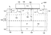
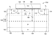
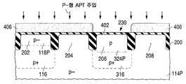
도 1 은, 미국 특허 제6,548,842 B1호 (Bulucea 등) 에 기재된 것과 같은 종래의 장 n-채널 IGFET (20) 를 도시한다. IGFET (20) 의 상부 표면에는, n-형 소스/드레인 ("S/D") 존 (26 및 28) 을 갖는 활성 반도체 아일랜드 (24) 를 측면으로 둘러싸는 리세스된 전기적 절연 필드-격리 영역 (22) 이 제공된다. 각각의 S/D 존 (26 또는 28) 은 매우 고농도로 도핑된 메인 부분 (26M 또는 28M) 및 보다 저농도로 도핑되지만 여전히 고농도로 도핑된 측면 연장부 (26E 또는 28E) 로 구성된다.1 shows a conventional long n-
S/D 존 (26 및 28) 은, 저농도로 도핑된 하부 부분 (34), 고농도로 도핑된 중간 웰 부분 (36), 및 상부 부분 (38) 로 이루어진 p-형 보디 재료 (32) 의 채널 존 (30) 에 의해 서로 분리되어 있다. 대부분의 상부 보디-재료 부분 (38) 이 적절하게 도핑되어 있지만, 부분 (38) 은 S/D 존 (26 및 28) 을 따라서 각각 연장하는 이온-주입되고 고농도로 도핑된 할로 포켓 부분 (40 및 42) 을 포함한다. IGFET (20) 은 게이트 유전체 층 (44), 그 위에 놓인 게이트 전극 (46), 전기적 절연 게이트 측벽 스페이서 (48 및 50), 및 금속 규소 화합물 층 (52, 54 및 56) 을 더 포함한다.S /
S/D 존 (26 및 28) 은 서로에 대해 대체로 미러 이미지이다. 또한, 채널 존 (30) 은 채널 도펀트 농도에 대해 대칭적으로 길이방향으로 분류되도록, 할로 포켓 부분 (40 및 42) 도 서로에 대해 대체로 미러 이미지이다. 그 결과, IGFET (20) 는 대칭 디바이스 (symmetric device) 이다. IGFET 동작 도중에, S/D 존 (26 또는 28) 둘 중 하나는 소스로서 동작할 수 있고, 다른 S/D 존 (28 또는 26) 은 드레인으로서 동작할 수 있다. 이는, S/D 존 (26 및 28) 각각이 특정 시간 주기 동안 소스 및 드레인으로서 각각 동작하고 다른 시간 주기 동안 드레인 및 소스로서 각각 동작하는 디지털 상황에 특히 적절하다. S /
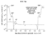
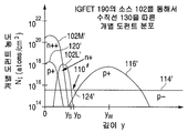
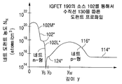
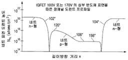
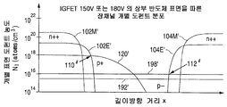
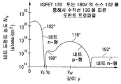
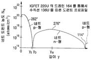
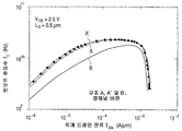
도 2 는, 네트 도펀트 농도 NN 이 IGFET (20) 에 대한 길이방향 거리 x 의 함수로서 어떻게 변화하는지를 도시한다. IGFET (20) 가 대칭 디바이스이기 때문에, 도 2 는 채널 중심으로부터 시작하여 1/2 프로파일만을 제시한다. 도 2 에서의 커브 세그먼트 26M*, 26E*, 28M*, 28E*, 30*, 40*, 및 42* 는 영역 26M, 26E, 28M, 28E, 30, 40, 및 42 의 네트 도펀트 농도를 각각 나타낸다. 점선 커브 세그먼트 40" 또는 42" 는 할로 포켓 (40 또는 42) 을 형성하는 p-형 도펀트의 전체 농도를 나타내고, 이는 포켓 (40 또는 42) 을 형성하는 사이에 S/D 존 (26 또는 28) 에 대한 위치로 도입된 p-형 도펀트를 포함한다.2 shows how the net dopant concentration N N varies as a function of the longitudinal distance x for the
IGFET (20) 내의 할로 포켓 (40 및 42) 의 존재는, 단채널 길이에서 임계 전압의 바람직하지 않은 롤 오프 (roll off) 를 경감시키는 것을 도울 뿐만 아니라, 채널 존 (30) 에서의 네트 p-형 도펀트 농도가 각각의 S/D 존 (26 또는 28), 특히 각의 측면 연장부 (26E 또는 28E) 를 따라서 증가되도록 야기시킨다. 이에 따라, 소스로서-동작하는 S/D 존 (26 또는 28) 을 따라서 연장하는 공핍 영역의 채널 존 부분의 두께가 감소하기 때문에, 펀치쓰루의 개시 (onset) 는 완화된다.The presence of
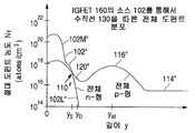
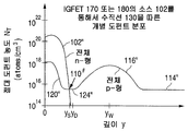
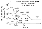
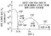
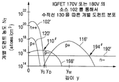
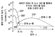
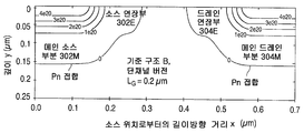
보디 재료 (30) 에는 펀치쓰루를 보다 더욱 완화시키기 위한 추가적인 도핑 특성이 제공된다. 미국 특허 제6,548,842 B1호에 나타난 정보에 기초하여, 도 3a 는 p-형 및 n-형 도펀트의 절대 농도 NT 가 추가적인 도핑 특성의 결과로서 메인 S/D 부분 (26M 또는 28M) 을 통해서 연장하는 수직선을 따른 깊이 y 의 함수로서 어떻게 변화하는지를 대략적으로 도시한다. 도 3a 에서의 커브 세그먼트 (26M" 또는 28M") 는 메인 S/D 부분 (26M 또는 28M) 을 정의하는 n-형 도펀트의 전체 농도를 나타낸다. 커브 세그먼트 (34", 36", 38", 40" 및 42") 는 함께 각각의 영역 (34, 36, 38, 40 및 42) 을 정의하는 p-형 도펀트의 전체 농도를 나타낸다.
추가적인 도핑 특성은, 상부 반도체 표면 아래로 0.1㎛ 초과의 깊이이지만 상부 표면 아래로 0.4㎛ 이하의 깊이에서 최고 농도에 도달하는 p-형 안티-펀치쓰루 ("APT; anti-punchthrouch") 도펀트로 p-형 상부 보디-재료 부분 (38) 을 이온 주입함으로써 달성된다. 메인 S/D 부분 (26M 및 28M) 이 상부 표면 아래로 대략적으로 0.2㎛ 연장하는 도 3a 에서 나타난 상황에서는, p-형 APT 도펀트가 대략적으로 0.2㎛ 의 깊이에서 최고 농도에 도달한다. 이러한 방식으로 p-형 APT 도펀트를 위치시킴으로써, 소스-동작하는 S/D 존 (26 또는 28) 의 pn 접합을 따라서 연장하는 공핍 영역의 채널-존 부분의 두께는 펀치쓰루를 더욱 완화시키도록 더 감소된다. Additional doping characteristics are p-type anti-punchthrough ("APT; anti-punchthrouch") dopants that reach a maximum concentration at depths greater than 0.1 μm below the top semiconductor surface but below 0.4 μm below the top surface. Is achieved by ion implanting the -shaped upper body-
p-형 APT 도펀트의 최고 농도의 깊이보다 아래의 깊이에서 최고 농도에 도달하는 p-형 웰 도펀트로 IGFET (20) 를 이온 주입함으로써 웰 영역 (36) 이 정의된다. p-형 웰 도펀트의 최고 농도가 p-형 APT 도펀트의 최고 농도보다 약간 높지만, 전체 p-형 도펀트의 수직 프로파일은 최고 웰-도펀트 농도의 위치에서 메인 S/D 부분 (26M 또는 28M) 까지 상대적으로 평평하다 (flat). 특히, 전체 p-형 도펀트의 NT 농도는 최고 웰-도펀트 농도의 위치에서 메인 S/D 부분 (26M 또는 28M) 까지 진행할 때 5 배보다 상당히 더 작게 감소한다.
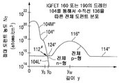
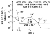
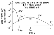
미국 특허 제6,548,842 B1호는, 메인 S/D 존 (26M 또는 28M) 을 통해서 전술한 수직선을 따른 p-형 도펀트 프로파일이 APT 와 웰 도펀트의 최고 농도들의 깊이들 사이의 깊이에서 최고 농도에 도달하는 추가적인 p-형 도펀트를 주입함으로써 더욱 평탄해질 수 있다는 것을 개시하고 있다. 이러한 상황은, 커브 세그먼트 58" 가 추가적인 p-형 도펀트에 의해 야기된 변동을 나타내는 이러한 IGFET (20) 의 변동에 대한 도 3b 에 도시된다. 도 3b 에서, 추가적인 p-형 도펀트의 최고 농도는 APT 와 웰 도펀트의 최고 농도들 사이에 있다. 따라서, 전체 p-형 도펀트의 NT 농도는 최고 웰-도펀트 농도의 위치로부터 메인 S/D 부분 (26M 또는 28M) 로 이동할 때 5 배보다 상당히 더 작게 감소한다.US Pat. No. 6,548,842 B1 discloses that the p-type dopant profile along the vertical line described above through the main S / D zone (26M or 28M) reaches the highest concentration at a depth between the depths of the highest concentrations of APT and well dopant. It is disclosed that it can be smoother by injecting additional p-type dopants. This situation is shown in Figure 3b for the variation of this
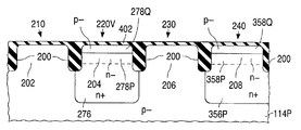
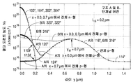
특히, 디바이스 동작 도중에 전류가 IGFET 를 통해서 일 방향으로만 흐르는 수많은 아날로그 용도의 상황에서는 대칭 IGFET 구조가 필요하지 않다. 미국 특허 제6,548,842 B1호에 개시된 바와 같이, 할로 포켓 부분은 드레인측에서 제거될 수 있다. 따라서, IGFET (20) 는 도 4a 에 도시된 바와 같이 장 N-채널 IGFET (60) 이 된다. 채널 존 (30) 이 비대칭적으로 길이방향으로 도펀트 분류되기 때문에, IGFET (60) 은 비대칭 디바이스이다. IGFET (60) 에서의 S/D 존 (26 및 28) 은 각각 소스 및 드레인으로서 기능한다. 도 4b 는 장채널 IGFET (60) 에 대응하는 비대칭 단 n-채널 IGFET (70) 을 도시한다. IGFET (70) 에서, 소스측 할로 포켓 (40) 은 드레인 (28) 에 근접하게 접근한다. IGFET (60 및 70) 에 대한 상부 반도체 표면을 따라서 길이방향 거리 x 의 함수로서의 네트 도펀트 농도 NN 가 각각 도 5a 및 도 5b 에 도시된다.In particular, for many analog applications where current flows only one way through the IGFET during device operation, a symmetrical IGFET structure is not needed. As disclosed in US Pat. No. 6,548,842 B1, the halo pocket portion can be removed at the drain side. Thus,
비대칭 IGFET (60 및 70) 은 대칭 IGFET (20) 와 동일한 APT 및 웰 주입부를 수용한다. 따라서, 소스 (26) 및 드레인 (28) 을 통해서 연장하는 수직선을 따라서, IGFET (60 및 70) 은, 점선 커브 세그먼트 (62") 가 할로 포켓 (42) 의 부재로 인해 드레인 (28) 을 통해서 수직 도펀트 분포를 나타내는 것을 제외하고는, 도 3a 에 도시된 도펀트 분포를 갖는다. IGFET 구조에 수직 도펀트 프로파일을 더욱 평탄화하기 위한 추가적인 웰 주입부가 제공되는 경우, 도 3b 는 드레인 (28) 을 통해서 도펀트 분포를 나타내는 커브 세그먼트 (62") 를 다시 행하는 필연적인 수직 도펀트 분포를 나타낸다.
미국 특허 제6,078,082호 및 제6,127,700호 (모두 Bulucea) 는 비대칭 채널 존을 갖지만 미국 특허 제6,548,842 B1호의 신규의 IGFET 에 사용되는 것과는 상이한 수직 도펀트 특성을 갖는 IGFET 를 설명한다. 또한, 비대칭 채널 존을 갖는 IGFET 는, (a) Buti 등에 의한 "Asymmetrical Halo Source GOLD drain (HS-GOLD) Deep Sub-half Micron n-MOSFET Design for Reliability and Performance" IEDM Tech . Dig ., 1989년 12월 3-6일, 26.2.1 - 26.2.4 페이지, (b) Chai 등에 의한 "A Cost-Effective 0.25㎛ Leff BiCMOS Technology Featuring Graded-Channel CMOS (GCMOS) and a Quasi-Self-Aligned (QSA) NPN for RF Wireless Applications", Procs . 2000 Bipolar / BiCMOS Circs . and Tech . Meeting, 2000년 9월 24-26일, 110 - 113 페이지, (c) Cheng 등에 의한 "Channel Engineering for High Speed Sub-1.0 V Power Supply Deep Submicron CMOS", 1999 Symp . VLSI Tech ., Dig . Tech . Paps ., 1999년 6월 14-16일, 69 및 70 페이지, (d) Deshpande 등에 의한 "Channel Engineering for Analog Device Design in Deep Submicron CMOS Technology for System on Chip Applications", IEEE Trans . Elec . Devs ., 2002년 9월, 1558 - 1565 페이지, (e) Hiroki 에 의한 "A High Performance 0.1㎛ MOSFET with Asymmetric Channel Profile", IEDM Tech . Dig ., 1995년 12월, 17.7.1 - 17.7.4 페이지, (f) Lamey 등에 의한 "Improving Manufacturability of an RF Graded Channel CMOS Process for Wireless Applications", SPIE Conf. Microelec. Dev. Tech. II, 1998년 9월, 147 - 155 페이지, (g) Ma 등에 의한, "Graded-Channel MOSFET(GCMOSFET) for High Performance, Low Voltage DSP Applications", IEEE Trans. VLSI Systs . Dig ., 1997년 12월, 352 - 358 페이지, (h) Matsuki 등에 의한 "Laterally-Doped Channel (LDC) Structure for Sub-Quarter Micron MOSFET", 1991 Symp. VLSI Tech ., Dig . Tech . Paps ., 1991년 5월 28-30일, 113 및 114 페이지, 및 (i) Su 등에 의한, "A High-Performance Scalable Submicron MOSFET for Mixed Analog/Digital Applications", IEDM Tech . Dig ., 1991년 12월, 367-370 페이지와 같은 다른 종래 문헌에서 검토된다.US Pat. Nos. 6,078,082 and 6,127,700 (both Bulucea) describe IGFETs with asymmetric channel zones but with different vertical dopant properties than those used in the novel IGFETs of US Pat. No. 6,548,842 B1. In addition, an IGFET having an asymmetric channel zone is (a) "Asymmetrical Halo Source GOLD drain (HS-GOLD) Deep Sub-half Micron n-MOSFET Design for Reliability and Performance" IEDM by Buti et al. Tech . Dig . , December 3-6, 1989, pages 26.2.1-26.2.4, (b) "A Cost-Effective 0.25 μm L eff BiCMOS Technology Featuring Graded-Channel CMOS (GCMOS) and a Quasi-Self- by Chai et al. Aligned (QSA) NPN for RF Wireless Applications ", Procs . 2000 Bipolar / BiCMOS Circs . and Tech . Meeting , 24-24 September 2000, pages 110-113, (c) "Channel Engineering for High Speed Sub-1.0 V Power Supply Deep Submicron CMOS" by Cheng et al . , 1999 Symp . VLSI Tech ., Dig . Tech . Paps . , June 14-16, 1999,
용어 "혼합 신호" 는 디지털 및 아날로그 회로 블록 모두를 포함하는 IC 를 지칭한다. 통상적으로, 디지털 회로는 주어진 전류 누설 사양에서 최대의 잠재적 디지털 속도를 획득하기 위해 가장 공격적으로 스케일링된 n-채널 및 p-채널 IGFET 를 사용한다. 아날로그 회로는 디지털 IGFET 과는 상이한 성능 요구조건들을 조건으로 하는 IGFET 및/또는 바이폴라 트랜지스터를 사용한다. 일반적으로, 아날로그 IGFET 에 대한 요구조건은 높은 선형 전압 이득, 높은 주파수에서의 양호한 소신호 및 대신호 주파수 응답, 양호한 파라미터 매칭, 낮은 입력 노이즈, 능동 및 수동 컴포넌트들에 대한 잘 제어된 전기적 파라미터, 감소된 기생장비들 (특히, 감소된 기생 커패시턴스) 을 포함한다. 아날로그 및 디지털 블록들에 대해 동일한 트랜지스터들을 사용하는 것이 경제적으로 이점이 있을 수도 있지만, 이렇게 하면 통상적으로 약해진 아날로그 성능을 야기한다. 아날로그 IGFET 성능에 부과된 수많은 요구조건들은 디지털 스케일링의 결과와 충돌한다.The term "mixed signal" refers to an IC that includes both digital and analog circuit blocks. Typically, digital circuits use the most aggressively scaled n-channel and p-channel IGFETs to obtain the maximum potential digital speed at a given current leakage specification. Analog circuits use IGFETs and / or bipolar transistors that are subject to different performance requirements than digital IGFETs. In general, the requirements for analog IGFETs include high linear voltage gain, good small and large signal frequency response at high frequencies, good parameter matching, low input noise, well controlled electrical parameters for active and passive components, and reduction. Parasitic devices (especially reduced parasitic capacitance). Using the same transistors for analog and digital blocks may be economically beneficial, but this typically results in weak analog performance. Many of the requirements imposed on analog IGFET performance conflict with the results of digital scaling.
그 중에서도, 아날로그 IGFET 의 전기적 파라미터는 디지털 블록에서의 IGFET 보다 더욱 정밀한 사양을 조건으로 한다. 증폭기로서 사용되는 아날로그 IGFET 에서, 그 고유 이득 (intrinsic gain) 을 최대화하기 위해 IGFET 의 출력 저항이 최대화될 필요가 있다. 그 출력 저항은, 또한 아날로그 IGFET 의 고주파수 성능을 설정하는데 있어서 중요하다. 반대로, 디지털 회로에서의 출력 저항은 상대적으로 중요성을 덜 가진다. 디지털 회로가 예를 들어 논리 "0" 및 논리 "1" 의 논리 상태를 구별할 수 있는 한, 더욱 높은 전류 구동 그리고 그 결과 더 높은 디지털 스위칭 속도 대신에 디지털 회로에서 출력 저항의 감소된 값이 허용될 수 있다.Among other things, the electrical parameters of analog IGFETs are subject to more precise specifications than IGFETs in digital blocks. In analog IGFETs used as amplifiers, the output resistance of the IGFET needs to be maximized to maximize its intrinsic gain. The output resistance is also important in setting the high frequency performance of the analog IGFET. In contrast, output resistance in digital circuits is of relatively less importance. As long as the digital circuit can distinguish the logic states of logic "0" and logic "1", for example, higher current driving and consequently reduced values of output resistance in the digital circuit instead of higher digital switching speeds are acceptable. Can be.
아날로그 트랜지스터를 통과하는 전기 신호의 형상은 회로 성능에 대해 중요하고, 보통 고조파 왜곡 (harmonic distortion) 및 노이즈가 없도록 가능한 한 합리적으로 유지되어야만 한다. 고조파 왜곡은 트랜지스터 이득 및 트랜지스터 커패시턴스의 비선형성에 의해 주로 야기된다. 따라서, 아날로그 트랜지스터에 대한 선형성 요구 정도는 매우 높다. pn 접합에서의 기생 커패시턴스는 아날로그 블록들에서 경감되어야 하는 고유의 전압 비선형성을 갖는다. 반대로, 디지털 회로에서의 신호 선형성은 통상적으로 이차적인 중요성을 갖는다.The shape of the electrical signal passing through the analog transistors is important for circuit performance and should be kept as reasonable as possible, usually free of harmonic distortion and noise. Harmonic distortion is mainly caused by the nonlinearity of transistor gain and transistor capacitance. Thus, the degree of linearity requirement for analog transistors is very high. Parasitic capacitances at pn junctions have inherent voltage nonlinearities that must be reduced in analog blocks. In contrast, signal linearity in digital circuits typically has secondary importance.
아날로그 증폭기에 사용되는 IGFET 의 소신호 아날로그 속도 성능은 소신호 주파수 한계에서 결정되고, 소스 및 드레인에 대한 pn 접합을 따라서 소신호 이득 및 기생 커패시턴스를 수반한다. 유사하게, 아날로그 증폭기 IGFET 의 대신호 아날로그 속도 성능은 대신호 주파수 한계에서 결정되고, IGFET 특성의 비선형성을 수반한다.The small signal analog speed performance of IGFETs used in analog amplifiers is determined at the small signal frequency limits and involves small signal gain and parasitic capacitance along the pn junction to the source and drain. Similarly, the large signal analog speed performance of the analog amplifier IGFET is determined at the large signal frequency limit and involves nonlinearity of the IGFET characteristics.
논리 게이트의 디지털 속도는 트랜지스터/부하 조합의 대신호 스위칭 시간에 관련하여 정의되고, 이에 따라, 구동 전류 및 출력 커패시턴스를 수반한다. 따라서, 아날로그 속도 성능은 디지털 속도 성능과는 다르게 결정된다. 아날로그 속도 및 디지털 속도에 대한 최적화는 상이할 수 있으며, 이는 상이한 트랜지스터 파라미터 요구조건을 요구하게 된다.The digital speed of the logic gate is defined in terms of the large signal switching time of the transistor / load combination, thus involving the drive current and the output capacitance. Thus, analog speed performance is determined differently than digital speed performance. Optimizations for analog speed and digital speed can be different, which will require different transistor parameter requirements.
디지털 회로 블록은 제조될 수 있는 초소형 IGFET 를 주로 사용한다. 그 결과 치수 확장 (dimensional spread) 이 본질적으로 크기 때문에, 디지털 회로에서의 파라미터 매칭은 종종 상대적으로 불량하다. 반대로, 아날로그 회로에서는 필수적인 성능을 달성하기 위해 양호한 파라미터 매칭이 일반적으로 필요하다. 이는, 통상적으로, 아날로그 트랜지스터는, 가능한 한 낮은 소스-드레인 전파 지연을 갖도록 하기 위해 아날로그 IGFET 를 가능한 한 짧게 하여 디지털 IGFET 보다 큰 치수로 제조되는 것이 요구된다.Digital circuit blocks mainly use tiny IGFETs that can be manufactured. As a result, the dimensional spread is inherently large, so parameter matching in digital circuits is often relatively poor. In contrast, in analog circuits, good parameter matching is generally needed to achieve the required performance. It is typically required that analog transistors be manufactured with dimensions larger than digital IGFETs by keeping the analog IGFET as short as possible in order to have as low a source-drain propagation delay as possible.
전술한 사항들의 관점에서, IGFET 에 양호한 아날로그 특성을 제공하는 반도체 아키텍쳐를 갖는 것이 바람직하다. 아날로그 IGFET 는, 높은 고유 이득, 높은 출력 저항, 감소된 기생 커패시턴스 (특히, 소스 및 드레인 접합을 따라서 감소된 기생 커패시턴스) 를 갖는 높은 소신호 속도를 가져야만 한다. 또한, 이 아키텍쳐는 고성능 디지털 IGFET 을 제공할 수 있는 것이 바람직하다.In view of the foregoing, it is desirable to have a semiconductor architecture that provides IGFETs with good analog characteristics. Analog IGFETs must have a high small signal rate with high intrinsic gain, high output resistance, and reduced parasitic capacitance (especially reduced parasitic capacitance along the source and drain junctions). It is also desirable that this architecture be able to provide high performance digital IGFETs.
본 발명은 이러한 아키텍쳐를 제공한다. 본 발명에 따르면, 반도체 구조체는 소스/드레인 바운더리를 형성하는 pn 접합들 중 적어도 하나의 pn 접합을 따라서 비교적 낮은 기생 커패시턴스를 갖는 주요 IGFET 를 포함한다. 디지털 용도로 이용가능하지만, 주요 IGFET 는 아날로그 용도에 특히 적합하고 우수한 아날로그 성능을 달성할 수 있다.The present invention provides such an architecture. In accordance with the present invention, the semiconductor structure includes a primary IGFET having a relatively low parasitic capacitance along the pn junction of at least one of the pn junctions forming the source / drain boundary. Although available for digital applications, the main IGFETs are particularly suitable for analog applications and can achieve good analog performance.
본 발명의 반도체 구조체는 주요 IGFET 와 유사하지만 반대 극성으로 구성된 추가적인 IGFET 을 포함할 수도 있다. 이에 따라, 2 개의 IGFET 는 아날로그 회로에 특히 유용한 상보형-IGFET 아키텍쳐를 형성한다. 본 발명의 반도체 구조체는 또한 디지털 회로에 특히 적합한 추가적인 IGFET, 또는 2 개의 추가적인 반대-극성의 IGFET 을 포함할 수도 있다. 따라서, 전반적인 아키텍쳐가 혼합 신호 IC 에서 사용될 수 있다.The semiconductor structure of the present invention may include additional IGFETs similar to the main IGFET but configured with opposite polarity. Accordingly, the two IGFETs form a complementary-IGFET architecture that is particularly useful for analog circuits. The semiconductor structure of the present invention may also include additional IGFETs, or two additional counter-polar IGFETs that are particularly suitable for digital circuits. Thus, the overall architecture can be used in mixed signal ICs.
주요 IGFET 로 돌아와서, 이는 채널 존, 한 쌍의 소스/드레인 ("S/D") 존, 채널 존 위에 놓인 게이트 유전체 층, 및 채널 존 상부의 게이트 유전체 층 위에 놓인 게이트 전극을 포함한다. 주요 IGFET 는, 제 1 도전형의 반도체 도펀트로 도핑된 보디 재료를 갖는 반도체 보디로부터 생성되어 제 1 도전형이 된다. 채널 존은 보디 재료의 일부이고 이에 따라 제 1 도전형이다. S/D 존은 반도체 보디의 상부 표면을 따라서 반도체 보디 내에 위치되고, 채널 존에 의해 측면 분리되어 있다. 각각의 S/D 존은 보디 재료와 pn 접합을 형성하도록 제 1 도전형에 반대인 제 2 도전형이다. 보디 재료는 S/D 존 아래에서 측면 연장한다.Returning to the main IGFET, it includes a channel zone, a pair of source / drain (“S / D”) zones, a gate dielectric layer overlying the channel zone, and a gate electrode overlying the gate dielectric layer over the channel zone. The main IGFET is produced from a semiconductor body having a body material doped with a semiconductor dopant of the first conductivity type to become the first conductivity type. The channel zone is part of the body material and thus is of the first conductivity type. The S / D zone is located in the semiconductor body along the upper surface of the semiconductor body and is laterally separated by the channel zone. Each S / D zone is of a second conductivity type opposite to the first conductivity type to form a pn junction with the body material. Body material extends laterally under the S / D zone.
중요하게, 보디 재료 내의 제 1 도전형의 도펀트는, 상부 반도체 표면 아래로 S/D 존들 중 특정 S/D 존보다 10 배 이하의 깊이에 있는, 바람직하게는 5 배 이하의 깊이에 있는 하부 보디-재료 위치로부터 그 특정 S/D 존으로 상향 이동할 때 적어도 1/10 로, 바람직하게는 적어도 1/20 로 감소하는 농도를 갖는다. 다시 말해서, 보디 재료 내의 제 1 도전형의 도펀트의 농도는, 특정 S/D 존보다 상부 반도체 표면 아래로 10 배 이하의 깊이, 바람직하게는 5 배 이하의 깊이에 있는 보디-재료 위치로 하향 이동할 때 적어도 10 배만큼, 바람직하게는 적어도 20 배만큼 증가한다. 보통, 이러한 서브표면 보디-재료 위치는 각각 채널 존 및 S/D 존 전체의 아래에 주로 놓여있다. 보디 재료에 이러한 "하이포어브럽트 (hypoabrupt)" 도펀트 분포를 제공함으로써, 보디 재료와 특정 S/D 존 사이의 pn 접합을 따른 기생 커패시턴스가 비교적 낮게 된다. 따라서, 주요 IGFET 는 높은 아날로그 성능을 달성할 수 있다.Importantly, the dopant of the first conductivity type in the body material is a lower body that is 10 times or less deep, preferably 5 times or less deeper than a particular S / D zone of the S / D zones below the upper semiconductor surface. Have a concentration decreasing at least 1/10, preferably at least 1/20 when moving upward from the material position to that particular S / D zone. In other words, the concentration of the dopant of the first conductivity type in the body material moves downward to the body-material position at a depth of 10 times or less, preferably 5 times or less, below the upper semiconductor surface than the particular S / D zone. When increased by at least 10 times, preferably at least 20 times. Usually, these subsurface body-material positions lie primarily below the channel zone and the entire S / D zone, respectively. By providing this "hypoabrupt" dopant distribution to the body material, the parasitic capacitance along the pn junction between the body material and the particular S / D zone is relatively low. Thus, major IGFETs can achieve high analog performance.
통상적으로, 주요 IGFET 는 채널 존이 비대칭적으로 길이방향으로 도펀트 분류되는 비대칭 디바이스이다. 구체적으로, 보디 재료 내의 제 1 도전형의 도펀트의 농도는, 채널 존이 상부 반도체 표면을 따라서 특정 S/D 존과 만나는 곳에서가 채널 존이 상부 표면을 따라서 S/D 존들 중 나머지 S/D 존과 만나는 곳에서보다 더 낮다. 따라서, 보통 IGFET 동작 도중에 특정 S/D 존이 드레인을 구성하는 동안 나머지 S/D 존은 소스를 구성한다. 보디 재료 내의 제 1 도전형의 도펀트의 농도는, 채널 존이 상부 표면을 따라서 소스와 만나는 곳에서보다 채널 존이 상부 표면을 따라서 드레인과 만나는 곳에서, 통상적으로 적어도 1/10 로 더 낮고, 바람직하게는 적어도 1/20 로 더 낮다. 다시 말해서, 보디 재료 내의 제 1 도전형의 도펀트의 농도는, 채널 존이 상부 표면을 따라서 드레인과 만나는 곳에서보다 채널 존이 채널 표면을 따라서 소스와 만나는 곳에서, 통상적으로 적어도 10 배 높고 바람직하게는 적어도 20 배 더 높다. Typically, the primary IGFET is an asymmetric device in which the channel zones are asymmetrically doped dopant longitudinally. Specifically, the concentration of the dopant of the first conductivity type in the body material is such that where the channel zone meets a particular S / D zone along the upper semiconductor surface and where the channel zone is along the top surface the remaining S / D of the S / D zones. Lower than where John meets. Thus, while a particular S / D zone constitutes a drain during IGFET operation, the remaining S / D zones constitute a source. The concentration of the dopant of the first conductivity type in the body material is typically lower, preferably at least 1/10, where the channel zone meets the drain along the top surface than where the channel zone meets the source along the top surface. Preferably at least 1/20 lower. In other words, the concentration of the dopant of the first conductivity type in the body material is typically at least 10 times higher and preferably where the channel zone meets the source along the channel surface than where the channel zone meets the drain along the upper surface. Is at least 20 times higher.
드레인으로부터의 전기력선이, 소스를 따른 공핍 영역의 이온화된 도펀트 원자를 제거하여 소스로부터 나오는 대부분의 전하 캐리어에 대한 전위 장벽의 절대값을 불리하게 저하시키는 대신에 소스 가까이에 있는 채널 존에 위치되고 소스 가까이에서 더 높은 채널-존 도펀트 농도를 제공하는 이온화된 도펀트 원자들을 제거하기 때문에, 채널 존의 소스측을 따른 높은 도펀트 농도는 드레인에서의 비교적 높은 전계로부터 소스를 보호한다. 이는 펀치쓰루를 경감시킨다. 이에 따라, 특정 S/D 존 (즉, 여기서는 드레인) 아래의 전술한 하이포어브럽트 수직 도펀트 프로파일과 소스측에서의 증가된 채널-존 도펀트 농도의 조합은 펀치쓰루 실패 없이 높은 아날로그 성능을 달성할 수 있다.The electric line of force from the drain is located in the channel zone near the source and is located in the channel zone near the source instead of removing the ionized dopant atoms in the depletion region along the source to adversely lower the absolute value of the potential barrier for most charge carriers coming from the source. Because it removes ionized dopant atoms that provide higher channel-zone dopant concentrations in close proximity, high dopant concentrations along the source side of the channel zone protect the source from relatively high electric fields in the drain. This alleviates punchthrough. Accordingly, the combination of the aforementioned hypobolite vertical dopant profile under a particular S / D zone (ie, drain here) and increased channel-zone dopant concentration at the source side can achieve high analog performance without punchthrough failure.
특정 S/D 존 아래의 하이포어브럽트 수직 도펀트 프로파일은 다양한 방법으로 구현될 수 있다. 일 구현에서, 보디 재료 내의 제 1 도전형의 도펀트의 농도는 특정 S/D 존 밑에 놓인 전술한 기판 보디-재료 위치에서 국지적 최대값에 도달한다. 그리고 보디 재료 내의 제 1 도전형의 도펀트의 농도는 통상적으로 그 보디-재료 위치로부터 특정 S/D 존으로 상향 이동할 때 급격하게 감소한다.The hypobolite vertical dopant profile under a particular S / D zone can be implemented in a variety of ways. In one implementation, the concentration of the dopant of the first conductivity type in the body material reaches a local maximum at the aforementioned substrate body-material location underneath a particular S / D zone. And the concentration of the dopant of the first conductivity type in the body material typically decreases sharply as it moves upward from its body-material position to a particular S / D zone.
본 발명에 따른 주요 IGFET 의 전술한 구현의 제조시에, 제 1 도전형의 반도체 웰 도펀트가 제 1 도전형의 웰 부분을 정의하기 위해 반도체 보디 내부로 통상적으로 이온 주입에 의해 도입된다. 웰-도핑을 수행하는데 있어서 이온 주입의 사용은 웰 도펀트가 전술한 서브표면 보디-재료 위치에서 그 최대 농도에 도달하는 것을 가능하게 한다. 게이트 전극은 채널 존이 되도록 의도된 반도체 재료의 상부에 제공되고, 반도체 재료와는 게이트 유전체 재료에 의해 분리된다. 제 2 도전형의 반도체 소스/드레인 도펀트가 반도체 보디로 도입되어 S/D 존을 형성한다.In the fabrication of the aforementioned implementation of the main IGFET according to the present invention, a semiconductor well dopant of the first conductivity type is typically introduced by ion implantation into the semiconductor body to define the well portion of the first conductivity type. The use of ion implantation in performing well-doping allows the well dopant to reach its maximum concentration at the aforementioned subsurface body-material locations. The gate electrode is provided on top of the semiconductor material intended to be a channel zone, and is separated from the semiconductor material by the gate dielectric material. A second conductive semiconductor source / drain dopant is introduced into the semiconductor body to form an S / D zone.
주요 IGFET 의 전술한 구현의 제조를 완성하기 위해 추가적인 프로세싱이 수행된다. 특정 S/D 영역 아래의 수직 도펀트 프로파일이 하이포어브럽트 가 되도록 야기하는 조건으로 웰-도핑 단계 및 추가적인 프로세싱이 행해진다. 특히, 웰 도펀트의 농도는 전술한 서브표면 보디-재료 위치로부터 특정 S/D 존으로 이동할 때 적어도 1/10 로 감소한다.Additional processing is performed to complete the fabrication of the aforementioned implementation of the main IGFET. The well-doping step and further processing are performed under conditions that cause the vertical dopant profile below the particular S / D region to be hypoblotted. In particular, the concentration of well dopant is reduced by at least 1/10 when moving from the aforementioned subsurface body-material position to a particular S / D zone.
적어도 IGFET 제조의 종료시점에서, 보디 재료는 제 1 도전형이다. IGFET 제조의 종료시점에서 보디 재료 및 S/D 존을 구성하는 반도체 재료는 초기에는 제 2 도전형일 수도 있다. 만일 그렇다면, 웰-도핑 단계는 이 재료의 하부 부분을 제 1 도전형으로 변환시킨다. 제조 프로세스의 일 버전에서, 이 재료의 나머지 상부 부분을 제 1 도전형으로 변환시키기 위해 제 1 도전형의 반도체 도펀트를 통해서 상보형 도핑이 수행된다. 제조 프로세스의 다른 버전에서, 웰 도펀트의 부분은 추가적인 프로세싱 도중에 이 재료의 상부 부분으로 상향 확산하고, 웰-도핑 단계에 후속하는 제 1 도전형 또는 제 2 도전형의 다른 도핑이 특히 수행하지 않은 이 재료의 상부 부분을 모두 사실상 제 1 도전형으로 변환시키도록 유도한다.At least at the end of IGFET fabrication, the body material is of a first conductivity type. The semiconductor material constituting the body material and the S / D zone at the end of IGFET fabrication may initially be of the second conductivity type. If so, the well-doping step converts the lower portion of this material to the first conductivity type. In one version of the fabrication process, complementary doping is performed through a semiconductor dopant of the first conductivity type to convert the remaining upper portion of the material to the first conductivity type. In another version of the fabrication process, the portion of the well dopant diffuses upwards to the upper portion of this material during further processing and is not particularly performed by other doping of the first conductivity type or second conductivity type following the well-doping step. Induce all of the upper portions of the material to be virtually converted to the first conductivity type.
주요 IGFET 의 다른 구현에서 보디 재료 내의 제 1 도전형의 도펀트의 농도는 전술한 서브표면 보디-재료 위치로부터 특정 S/D 존으로 상향 이동할 때 스텝 감소 (step decrease) 를 실질적으로 경험한다. 예를 들어, 보디 재료는, 서브표면 (매립된) 보디-재료 부분, 그리고 상부 반도체 표면으로 연장하고 S/D 를 포함하는 그 서브표면 보디-재료 부분 바로 위에 놓인 서브-인접 보디-재료 부분을 포함할 수도 있다. 서브표면 보디-재료 부분은, S/D 존의 밑에 놓이고, 그 가장 가까운 곳에서, 상부 반도체 표면 아래로 S/D 존 보다 10 배 이하의 깊이, 바람직하게는 5 배 이하의 깊이에 있다. 서브표면 보디-재료 부분은 예를 들어 주로 균일하게 도핑될 수 있다. 다음으로, 보디 재료 내의 제 1 도전형의 도펀트의 농도는, 서브표면 보디-재료 부분으로부터 표면-인접 보디-재료 부분으로 가로지르는 중에, 그리고 표면-인접 보디-재료 부분을 통해서 특정 S/D 존으로 더욱 상향하여 이동할 때 보통 적어도 1/10 로 스텝 감소를 실질적으로 경험하고, 서브표면 보디-재료 부분 내에서보다 적어도 10 배 더 작게 유지한다.In another implementation of the main IGFET, the concentration of the dopant of the first conductivity type in the body material substantially experiences a step decrease as it moves upward from the subsurface body-material location to the particular S / D zone. For example, the body material may comprise a subsurface (embedded) body-material portion and a sub-adjacent body-material portion extending directly to the upper semiconductor surface and overlying the subsurface body-material portion including S / D. It may also include. The subsurface body-material portion lies underneath the S / D zone and, at its closest, at a depth of 10 times or less, preferably 5 times or less, below the upper semiconductor surface than the S / D zone. The subsurface body-material portion may for example be predominantly uniformly doped. Next, the concentration of the dopant of the first conductivity type in the body material is intersected from the sub-surface body-material portion to the surface-adjacent body-material portion, and through the surface-adjacent body-material portion, through the specific S / D zone. And substantially experience step reduction at least 1/10 when moving further upwards, and remain at least 10 times smaller than in the subsurface body-material portion.
다시 말해서, 본 발명은, 아날로그 회로에 특히 적절하고, IGFET, 또는 한 쌍의 반대-극성의 IGFET 을 갖는 반도체 아키텍쳐를 충족시킨다. 본 아키텍쳐는, 디지털 회로에 특히 적절한, 추가적인 IGFET, 또는 한 쌍의 반대-극성의 추가적인 IGFET 을 포함할 수도 있다. 결과 아키텍쳐는 혼합-신호 용도를 매우 잘 처리할 수 있다. 따라서, 본 발명은 종래 기술 전반에 대한 상당한 진보를 제공한다.In other words, the present invention is particularly suitable for analog circuits and meets a semiconductor architecture having an IGFET, or a pair of anti-polar IGFETs. The architecture may include additional IGFETs, or a pair of counter-polar additional IGFETs, which are particularly suitable for digital circuits. The resulting architecture can handle mixed-signal applications very well. Thus, the present invention provides a significant advance over the prior art.
도 1 은 종래 기술 대칭 장 n-채널 IGFET 의 전방 단면도이다.
도 2 는, 도 1 의 IGFET 에 대한 채널 중심으로부터 길이방향 거리의 함수로서의 상부 반도체 표면을 따라서 네트 도펀트 농도의 그래프이다.
도 3a 및 도 3b 는, 도 1, 도 4a 및 도 4b 의 IGFET 에 대한 2 개의 각각 상이한 웰-도핑 조건에서 소스/드레인 존을 통한 수직선을 따른 깊이의 함수로서의 절대 도펀트 농도의 그래프이다.
도 4a 및 도 4b 는 각각의 종래 기술 비대칭 장 n-채널 IGFET 및 종래 기술 비대칭 단 n-채널 IGFET 의 전방 단면도이다.
도 5a 및 도 5b 는, 도 4a 및 도 4b 의 각각의 IGFET 에 대한 채널 중심으로부터 길이방향 거리의 함수로서의 상부 반도체 표면을 따른 네트 도펀트 농도의 그래프이다.
도 6 은 바로 아래 놓인 반도체 재료와 동일한 도전형의 반도체 웰 부분을 갖도록 본 발명에 따라서 구성된 비대칭 장 n-채널 IGFET 의 전방 단면도이다.
도 7a 내지 도 7c 는, 도 6, 도 18a, 도 68a 또는 도 68b 의 IGFET 에 대한 상부 반도체 표면을 따라서 길이방향 거리의 함수로서의 개별 도펀트 농도, 절대 도펀트 농도 및 네트 도펀트 농도의 각각의 그래프이다.
도 8a 내지 도 8c 는, 도 6, 도 11 또는 도 13 의 IGFET 의 소스를 통해서 수직선을 따른 깊이의 함수로서의 개별 도펀트 농도, 절대 도펀트 농도 및 네트 도펀트 농도의 각각의 그래프이다.
도 9a 내지 도 9c 는, 도 6, 도 11, 도 13 또는 도 15 의 IGFET 의 채널 존을 통한 한 쌍의 수직선을 따른 깊이의 함수로서의 개별 도펀트 농도, 절대 도펀트 농도 및 네트 도펀트 농도의 각각의 그래프이다.
도 10a 내지 도 10c 는, 도 6, 도 11, 도 13, 도 18a 또는 도 18b 의 IGFET 의 드레인을 통한 수직선을 따른 깊이의 함수로서의 개별 도펀트 농도, 절대 도펀트 농도 및 네트 도펀트 농도의 각각의 그래프이다.
도 11 은 바로 아래 놓인 반도체 재료와 동일한 도전형의 반도체 웰 부분을 갖도록 본 발명에 따라서 구성된 비대칭 단 n-채널 IGFET 의 전방 단면도이다.
도 12a 내지 도 12c 는, 도 11 의 IGFET 에 대한 상부 반도체 표면을 따라서 길이방향 거리의 함수로서의 개별 도펀트 농도, 절대 도펀트 농도 및 네트 도펀트 농도의 각각의 그래프이다.
도 13 은 바로 아래 놓인 반도체 재료와 동일한 도전형의 반도체 웰 부분을 갖도록 본 발명에 따라서 구성된 다른 비대칭 장 n-채널 IGFET 의 전방 단면도이다.
도 14a 내지 도 14c 는, 도 13, 도 15, 도 18b 또는 도 18c 에 대한 상부 반도체 표면을 따라서 길이방향 거리의 함수로서의 개별 도펀트 농도, 절대 도펀트 농도 및 네트 도펀트 농도의 각각의 그래프이다.
도 15 는 바로 아래 놓인 반도체 재료와 동일한 도전형의 반도체 웰 부분을 갖도록 본 발명에 따라서 구성된 추가적인 비대칭 장 n-채널 IGFET 의 전방 단면도이다.
도 16a 내지 도 16c 는, 도 15 의 IGFET 의 드레인을 통해서 연장하는 수직선을 따른 깊이의 함수로서의 개별 도펀트 농도, 절대 도펀트 농도 및 네트 도펀트 농도의 각각의 그래프이다.
도 17a 내지 도 17c 는, 도 15 또는 도 18c 의 IGFET 의 드레인을 통해서 연장하는 수직선을 따른 깊이의 함수로서의 개별 도펀트 농도, 절대 도펀트 농도 및 네트 도펀트 농도의 각각의 그래프이다.
도 18a 내지 도 18c 는, 바로 아래 놓인 반도체 재료와 동일한 도전형의 반도체 웰 부분을 각각 갖도록 본 발명에 따라서 구성된 3 개의 개별적인 장 n-채널 IGFET 의 전방 단면도이다.
도 19a 내지 도 19c 는, 도 18a 또는 도 18b 의 IGFET 의 소스를 통해서 연장하는 수직선을 따른 깊이의 함수로서의 개별 도펀트 농도, 절대 도펀트 농도 및 네트 도펀트 농도의 각각의 그래프이다.
도 20a 내지 도 20c 는, 도 18c 의 IGFET 의 소스를 통해서 연장하는 수직선을 따른 깊이의 함수로서의 개별 도펀트 농도, 절대 도펀트 농도 및 네트 도펀트 농도의 각각의 그래프이다.
도 21 은 바로 아래 놓인 반도체 재료와 반대의 도전형의 반도체 웰 부분을 갖도록 본 발명에 따라서 구성된 비대칭 장 n-채널 IGFET 의 전방 단면도이다.
도 22a 내지 도 22c 는, 도 21 또는 도 27a 의 IGFET 에 대해 상부 반도체 표면을 따라서 길이방향 거리의 함수로서의 개별 도펀트 농도, 절대 도펀트 농도 및 네트 도펀트 농도의 각각의 그래프이다.
도 23a 내지 도 23c 는, 도 21 또는 도 25 의 IGFET 의 소스를 통한 수직선을 따른 깊이의 함수로서의 개별 도펀트 농도, 절대 도펀트 농도 및 네트 도펀트 농도의 각각의 그래프이다.
도 24a 내지 도 24c 는, 도 21, 도 25, 도 27a 또는 도 27b 의 드레인을 통한 수직선을 따른 깊이의 함수로서의 개별 도펀트 농도, 절대 도펀트 농도 및 네트 도펀트 농도의 각각의 그래프이다.
도 25 는 바로 아래 놓인 반도체 재료와 반대의 도전형의 반도체 웰 부분을 갖도록 본 발명에 따라서 구성된 다른 비대칭 장 n-채널 IGFET 의 전방 단면도이다.
도 26a 내지 도 26c 는, 도 25 또는 도 27b 의 IGFET 에 대한 상부 반도체 표면을 따라서 길이방향 거리의 함수로서의 개별 도펀트 농도, 절대 도펀트 농도 및 네트 도펀트 농도의 각각의 그래프이다.
도 27a 및 도 27b 는 바로 아래 놓인 반도체 재료와 반대의 도전형의 반도체 웰 부분을 각각 갖도록 본 발명에 따라서 구성된 2 개의 개별적인 장 n-채널 IGFET 의 전방 단면도이다.
도 28a 내지 도 28c 는, 도 27a 또는 도 27b 의 IGFET 의 소스를 통해서 연장하는 수직선을 따른 깊이의 함수로서의 개별 도펀트 농도, 절대 도펀트 농도 및 네트 도펀트 농도의 각각의 그래프이다.
도 29 의 29.1 및 29.2 는 본 발명에 따라서 구성된 상보형-IGFET 반도체 구조의 2 부분의 전방 단면도이다.
도 30 의 30.1 및 30.2 는 본 발명에 따라서 구성된 다른 상보형-IGFET 반도체 구조의 2 개의 부분의 전방 단면도이다.
도 31a 내지 도 31o, 도 31p.1 내지 도 31r.1, 및 도 31p.2 내지 도 31r.2 는, 도 29.1 및 도 29.2 의 상보형-IGFET 반도체 구조를 제조하는 단계들을 나타내는 전방 단면도이다. 도 31a 내지 도 31o 의 단계들은 도 29.1 및 도 29.2 모두에서 도시된 구조 부분에 적용된다. 도 31p.1 내지 도 31r.1 는 도 29.1 의 구조 부분으로 유도하는 추가적인 단계들을 나타낸다. 도 31p.2 내지 도 31r.2 는 도 29.2 의 구조 부분으로 유도하는 추가적인 단계들을 나타낸다.
도 32a 내지 도 32c 는, 본 발명에 따라서, 도 32a 로서 반복된 도 31d 의 구조를 통해서 시작하는 도 29.1 및 도 29.2 의 상보형-IGFET 반도체 구조의 변화를 제조하는 도 31e 의 단계들에 대한 대안적인 단계들을 나타내는 전방 단면도이다.
도 33a 내지 도 33f 는, 본 발명에 따라서, 도 33a 로서 반복된 도 31b 의 구조를 통해서 시작하는 도 29.1 및 도 29.2 의 상보형-IGFET 반도체 구조의 변화를 제조하는 도 31c 내지 도 31f 의 단계들에 대한 다른 대안적인 단계들을 나타내는 전방 단면도이다.
도 34 는, 바로 아래 놓인 반도체 재료와 반대의 도전형의 반도체 웰 부분을 갖도록 본 발명에 따라서 구성되고, 초기에 정의된 바와 같이 웰 부분 상부의 반도체 재료로 상보형 n-형 도펀트 주입을 하지 않고 본 발명에 따라서 제조된 비대칭 장 p-형 IGFET 의 전방 단면도이다. 도 32a 내지 도 32c 또는 도 33a 내지 도 33f 의 대안적인 단계들을 사용하여 도 31a 내지 도 31o, 도 31p.1 내지 도 31r.1 및 도 31p.2 내지 도 31r.2 의 프로세스에 따라서 제조된 비대칭 p-채널 IGFET 는, 도 34 의 p-채널 IGFET 의 구현이다.
도 35a 내지 도 35c 는, 도 34 의 IGFET 에 대한 상부 반도체 표면을 따라서 길이방향 거리의 함수로서의 개별 도펀트 농도, 절대 도펀트 농도 및 네트 도펀트 농도의 각각의 그래프이다.
도 36a 내지 도 36c 는, 도 34 의 IGFET 의 소스를 통한 수직선을 따른 깊이의 함수로서의 개별 도펀트 농도, 절대 도펀트 농도 및 네트 도펀트 농도의 각각의 그래프이다.
도 37a 내지 도 37c 는, 도 34 의 IGFET 의 채널 존을 통한 한 쌍의 수직선을 따른 깊이의 함수로서의 개별 도펀트 농도, 절대 도펀트 농도 및 네트 도펀트 농도의 각각의 그래프이다.
도 38a 내지 도 38c 는 도 34 의 IGFET 의 드레인을 통한 수직선을 따른 깊이의 함수로서의 개별 도펀트 농도, 절대 도펀트 농도 및 네트 도펀트 농도의 각각의 그래프이다.
도 39 및 도 40 은, (i) 본 발명에 따라서 구성된 비대칭 단 n-채널 IGFET 및 (ii) 기준 대칭 단 n-채널 IGFET 의 각각의 컴퓨터 시뮬레이션에 대한 깊이와 길이방향 거리의 함수로서의 네트 도펀트 농도의 3 차원 그래프이다.
도 41 및 도 42 는, 도 39 및 도 40 의 각각의 컴퓨터-시뮬레이팅된 IGFET 에 대한 소스 위치로부터 깊이와 길이방향 거리의 함수로서의 도펀트 등고선 (dopant contour) 을 나타내는 그래프이다.
도 43 은, 도 39 및 도 40 의 컴퓨터-시뮬레이팅된 IGFET 에 대한 소스 위치로부터 길이방향 거리의 함수로서의 네트 도펀트 농도의 그래프이다.
도 44a 및 도 44b 는, 도 39 및 도 40 의 컴퓨터-시뮬레이팅된 IGFET 에 대한 각각의 소스 및 드레인을 통한 한 쌍의 수직선을 따른 깊이의 함수로서의 절대 도펀트 농도 및 네트 도펀트 농도의 각각의 그래프이다.
도 45a 및 도 45b 는, 도 39 및 도 40 의 컴퓨터-시뮬레이팅된 IGFET 에 대한 각각의 임계 및 포화 조건에서 게이트-소스 전압의 함수로서의 직계의 트랜스컨덕턴스 및 직계의 드레인 전류의 그래프이다.
도 46a 및 도 46b 는, (i) 도 39 의 신규의 단채널 IGFET 에 일반적으로 대응하는 신규의 비대칭 장 n-채널 IGFET 및 (ii) 도 40 의 기준 단채널 IGFET 에 일반적으로 대응하는 기준 대칭 장 n-채널 IGFET 의 컴퓨터 시뮬레이션에 대한 임계 조건 및 포화 조건 각각에서 게이트-소스 전압의 함수로서의 직계의 트랜스컨덕턴스 및 직계의 드레인 전류의 그래프이다.
도 47 은, (i) 도 39 의 신규의 IGFET, (ii) 도 40 의 기준 IGFET, 및 (iii) 안티-펀치쓰루 주입이 부족한 추가적인 기준 대칭 단 n-채널 IGFET 의 컴퓨터 시뮬레이션들에 대한 게이트-소스 전압의 함수로서의 직계의 드레인 전류 밀도의 그래프이다.
도 48 은, 도 39 및 도 40 의 컴퓨터-시뮬레이팅된 IGFET 에 대한 드레인-소스 전압의 함수로서의 선형 드레인 전류의 그래프이다.
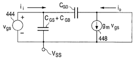
도 49 는 n-채널 IGFET 및 관련 기생 커패시턴스의 회로도이다.
도 50 은, 도 49 의 n-채널 IGFET 및 관련 기생 커패시턴스의 소신호 모델의 회로도이다.
도 51a 내지 도 51c 는, 각각 공통-소스, 공통-게이트, 및 공통 드레인 구성으로 배열된 단일-IGFET 증폭기의 회로도이다.
도 52 는 공통-소스 단락-출력 구성으로 배열된 단일-IGFET 증폭기의 회로도이다.
도 53 은 도 52 의 증폭기의 소신호 모델의 회로도이다.
도 54 는 3 개의 상이한 p-형 도펀트 분포의 모델들에 대한 pn 접합으로부터의 거리의 함수로서의 네트 도펀트 농도의 그래프이다.
도 55 는 도 54 의 3 개의 도펀트 분포의 모델들에 대한 역전압의 함수로서의 공핍-층 커패시턴스의 그래프이다.
도 56 은 저농도로 도핑된 측 (more lightly doped side) 이 도펀트 농도의 단계적인 변화를 경험하는 접합 커패시터의 모델에 대한 pn 접합으로부터의 거리의 함수로서의 네트 보디 도펀트 농도의 그래프이다.
도 57 은 도 56 에서 모델링된 접합 커패시터에 대한 역전압의 함수로서의 지역의 접합 커패시턴스의 그래프이다.
도 58a 및 도 58b 는, 본 발명에 따라서 구성된 각각의 비대칭 단 n-채널 IGFET 및 비대칭 장 n-채널 IGFET 의 컴퓨터 시뮬레이션에 대한 채널 중심으로부터의 깊이 및 길이방향 거리의 함수로서의 도펀트 등고선의 복합 전방 단면도/그래프이다.
도 59 는, 도 39 및 도 40 의 컴퓨터-시뮬레이팅된 IGFET 에 대한 드레인-보디 전압의 함수로서의 직계의 드레인-보디 커패시턴스의 그래프이다.
도 60 은, 도 39 및 도 40 의 컴퓨터-시뮬레이팅된 IGFET 에 대한 소스-보디 전압의 함수로서의 직계의 소스-보디 커패시턴스의 그래프이다.
도 61 은, 도 39 및 도 40 의 컴퓨터-시뮬레이팅된 IGFET 및 도 63 의 추가적인 신규의 IGFET 에 대한 직계의 드레인 전류의 함수로서의 컷-오프 주파수의 그래프이다.
도 62 는, (i) 도 39 의 신규의 단채널 IGFET 에 대응하는 신규의 비대칭 장 n-채널 IGFET, (ii) 도 40 의 기준 단채널 IGFET 에 대응하는 기준 대칭 장 n-채널 IGFET, 및 (iii) 도 63 의 추가적인 신규의 단채널 IGFET 에 대응하는 추가적인 신규의 비대칭 장 n-채널 IGFET 의 컴퓨터 시뮬레이션에 대한 직계의 드레인 전류의 함수로서의 컷-오프 주파수의 그래프이다.
도 63 은 본 발명에 따라서 구성된 다른 컴퓨터-시뮬레이팅된 비대칭 단 n-채널 IGFET 의 전방 단면도이다.
도 64 는, 도 39 및 도 63 의 컴퓨터-시뮬레이팅된 IGFET 에 대한 소스 위치로부터 길이방향 거리의 함수로서의 네트 도펀트 농도의 그래프이다.
도 65 는, (i) 본 발명에 따라서 구성된 비대칭 n-채널 IGFET, (ii) 각각의 소스/드레인 존을 따라서 할로 포켓 부분을 갖는 기준 대칭 n-채널 IGFET, 및 (iii) 각각의 소스/드레인 존을 따라서 할로 포켓이 부족한 기준 대칭 n-채널 IGFET 에 대한 채널 길이의 함수로서의 임계 전압의 그래프이다.
도 66 은 본 발명에 따라서 구성된 추가적인 상보형-IGFET 반도체 구조의 전방 단면도이다.
도 67 은, (i) 본 발명에 따라서 구성된 2 개의 비대칭 n-채널 IGFET 및 (ii) 기준 대칭 n-채널 IGFET 에 대한 깊이의 함수로서의 절대 도펀트 농도의 그래프이다.
도 68a 및 도 68b 는 본 발명에 따라서 구성된 2 개의 개별 추가적인 비대칭 장 n-채널 IGFET 의 전방 단면도이다.
도 69a 내지 도 69c 는, 도 68a 또는 도 68b 의 IGFET 의 소스를 통해서 수직선을 따른 깊이의 함수로서의 개별 도펀트 농도, 절대 도펀트 농도, 및 네트 도펀트 농도의 각각의 그래프이다.
도 70a 내지 도 70c 는, 도 68a 또는 도 68b 의 채널 존을 통해 한 쌍의 수직선을 따른 깊이의 함수로서의 개별 도펀트 농도, 절대 도펀트 농도, 및 네트 도펀트 농도의 각각의 그래프이다.
도 71a 내지 도 71c 는, 도 68a 또는 도 68b 의 IGFET 의 드레인을 통해서 연장하는 수직선을 따른 깊이의 함수로서의 개별 도펀트 농도, 절대 도펀트 농도, 및 네트 도펀트 농도의 각각의 그래프이다.
도 72a 내지 도 72d 는 본 발명에 따라서 구성된 4 개의 추가적인 개별 상보형-IGFET 의 전방 단면도이다.
동일하거나 또는 매우 유사한 아이템 또는 아이템들을 나타내기 위해 바람직한 실시형태의 상세한 설명 및 도면에 유사한 참조 기호가 사용된다. 그래프들을 포함하는 도면에서 단일 프라임 ('), 더블 프라임 ("), 별표 (*), 및 파운드 (#) 사인을 갖는 참조 기호의 수치 부분은 각각 다른 도면에서 유사하게 넘버링된 영역 또는 존을 나타낸다. 반도체 웰 도펀트가 제공된 IGFET 의 단면도에서의 "X" 는 웰 도펀트의 최대 농도의 위치를 나타낸다. 전기적 격리 스페이서 (미도시) 가, 이들 IGFET 의 제조 방법에 기초하여 도 13, 도 15, 도 18b, 도 18c, 도 25, 도 27b 및 도 34 의 IGFET 의 게이트 전극의 측벽을 따라서 위치될 수도 있다.
도펀트-분포 그래프에서, "개별적인" 도펀트 농도는 각각 따로 도입된 n-형 도펀트 및 각각 따로 도입된 p-형 도펀트의 개별적인 농도를 의미하고, "절대" 도펀트 농도는 전체 n-형 도펀트 농도 및 전체 p-형 도펀트 농도를 의미한다. 도펀트-분포 그래프에서 "네트" 도펀트 농도는 절대 (또는 전체) n-형 도펀트 농도 및 절대 (또는 전체) p-형 도펀트 농도 사이의 차이이다. 네트 도펀트 농도는, 절대 n-형 도펀트 농도가 절대 p-형 도펀트 농도를 초과할 때는 네트 "n-형" 으로서 표시되고, 절대 p-형 도펀트 농도가 절대 n-형 도펀트 농도를 초과할 때는 네트 "p-형" 으로서 표시된다.1 is a front cross-sectional view of a prior art symmetric long n-channel IGFET.
FIG. 2 is a graph of net dopant concentration along the upper semiconductor surface as a function of longitudinal distance from the channel center for the IGFET of FIG. 1.
3A and 3B are graphs of absolute dopant concentration as a function of depth along the vertical line through the source / drain zone at two different well-doping conditions for the IGFETs of FIGS. 1, 4A and 4B.
4A and 4B are front cross-sectional views of each prior art asymmetric long n-channel IGFET and prior art asymmetric short n-channel IGFET.
5A and 5B are graphs of net dopant concentration along the upper semiconductor surface as a function of longitudinal distance from the channel center for each IGFET of FIGS. 4A and 4B.
6 is a front cross-sectional view of an asymmetric long n-channel IGFET constructed in accordance with the present invention to have a semiconductor well portion of the same conductivity type as the underlying semiconductor material.
7A-7C are respective graphs of individual dopant concentrations, absolute dopant concentrations, and net dopant concentrations as a function of longitudinal distance along the upper semiconductor surface for the IGFET of FIGS. 6, 18A, 68A, or 68B.
8A-8C are respective graphs of individual dopant concentrations, absolute dopant concentrations, and net dopant concentrations as a function of depth along the vertical line through the source of the IGFET of FIG. 6, 11, or 13.
9A-9C are respective graphs of individual dopant concentrations, absolute dopant concentrations, and net dopant concentrations as a function of depth along a pair of vertical lines through the channel zone of the IGFET of FIGS. 6, 11, 13, or 15; to be.
10A-10C are respective graphs of individual dopant concentrations, absolute dopant concentrations, and net dopant concentrations as a function of depth along a vertical line through the drain of the IGFET of FIGS. 6, 11, 13, 18A, or 18B. .
11 is a front cross-sectional view of an asymmetrical short n-channel IGFET constructed in accordance with the present invention to have a semiconductor well portion of the same conductivity type as the underlying semiconductor material.
12A-12C are respective graphs of individual dopant concentrations, absolute dopant concentrations, and net dopant concentrations as a function of longitudinal distance along the upper semiconductor surface for the IGFET of FIG. 11.
13 is a front cross-sectional view of another asymmetric long n-channel IGFET configured in accordance with the present invention to have a semiconductor well portion of the same conductivity type as the underlying semiconductor material.
14A-14C are respective graphs of individual dopant concentrations, absolute dopant concentrations and net dopant concentrations as a function of longitudinal distance along the upper semiconductor surface for FIGS. 13, 15, 18B or 18C.
15 is a front cross-sectional view of an additional asymmetric long n-channel IGFET configured in accordance with the present invention to have a semiconductor well portion of the same conductivity type as the underlying semiconductor material.
16A-16C are respective graphs of individual dopant concentrations, absolute dopant concentrations, and net dopant concentrations as a function of depth along a vertical line extending through the drain of the IGFET of FIG. 15.
17A-17C are respective graphs of individual dopant concentrations, absolute dopant concentrations, and net dopant concentrations as a function of depth along a vertical line extending through the drain of the IGFET of FIG. 15 or 18C.
18A-18C are front cross-sectional views of three separate long n-channel IGFETs constructed in accordance with the present invention, each having a semiconductor well portion of the same conductivity type as the underlying semiconductor material.
19A-19C are respective graphs of individual dopant concentrations, absolute dopant concentrations, and net dopant concentrations as a function of depth along a vertical line extending through the source of the IGFET of FIG. 18A or 18B.
20A-20C are respective graphs of individual dopant concentrations, absolute dopant concentrations, and net dopant concentrations as a function of depth along a vertical line extending through the source of the IGFET of FIG. 18C.
21 is a front cross-sectional view of an asymmetric long n-channel IGFET constructed in accordance with the present invention having a semiconductor well portion of a conductivity type opposite to the underlying semiconductor material.
22A-22C are respective graphs of individual dopant concentrations, absolute dopant concentrations, and net dopant concentrations as a function of longitudinal distance along the upper semiconductor surface for the IGFET of FIG. 21 or 27A.
23A-23C are respective graphs of individual dopant concentrations, absolute dopant concentrations, and net dopant concentrations as a function of depth along a vertical line through the source of the IGFET of FIG. 21 or 25.
24A-C are respective graphs of individual dopant concentrations, absolute dopant concentrations, and net dopant concentrations as a function of depth along the vertical line through the drain of FIGS. 21, 25, 27A, or 27B.
25 is a front cross-sectional view of another asymmetric long n-channel IGFET configured in accordance with the present invention having a semiconductor well portion of a conductivity type opposite to the underlying semiconductor material.
26A-26C are respective graphs of individual dopant concentrations, absolute dopant concentrations, and net dopant concentrations as a function of longitudinal distance along the upper semiconductor surface for the IGFET of FIG. 25 or 27B.
27A and 27B are front cross-sectional views of two separate long n-channel IGFETs constructed in accordance with the present invention, each having a semiconductor well portion of a conductivity type opposite to the underlying semiconductor material.
28A-28C are respective graphs of individual dopant concentrations, absolute dopant concentrations, and net dopant concentrations as a function of depth along a vertical line extending through the source of the IGFET of FIG. 27A or 27B.
29.1 and 29.2 of FIG. 29 are front cross-sectional views of two portions of a complementary-IGFET semiconductor structure constructed in accordance with the present invention.
30.1 and 30.2 of FIG. 30 are front cross-sectional views of two portions of another complementary-IGFET semiconductor structure constructed in accordance with the present invention.
31A to 31O, 31P.1 to 31R.1, and 31P.2 to 31R.2 are front cross-sectional views illustrating steps of fabricating the complementary-IGFET semiconductor structure of FIGS. 29.1 and 29.2. The steps of FIGS. 31A-31O apply to the structural portions shown in both FIGS. 29.1 and 29.2. 31p.1-31r.1 show additional steps leading to the structural part of FIG. 29.1. 31p.2 to 31r.2 show additional steps leading to the structural part of FIG. 29.2.
32A-32C are alternatives to the steps of FIG. 31E for fabricating changes in the complementary-IGFET semiconductor structure of FIGS. 29.1 and 29.2 starting with the structure of FIG. 31D repeated as FIG. 32A in accordance with the present invention. Is a front cross-sectional view showing the typical steps.
33A-33F illustrate the steps of FIGS. 31C-31F to fabricate a change in the complementary-IGFET semiconductor structure of FIGS. 29.1 and 29.2 starting through the structure of FIG. 31B repeated as FIG. 33A in accordance with the present invention. A front cross-sectional view showing other alternative steps for.
34 is configured in accordance with the present invention to have a semiconductor well portion of a conductivity type opposite to the semiconductor material immediately underlying and without complementary n-type dopant implantation into the semiconductor material over the well portion as defined earlier. A front cross sectional view of an asymmetric long p-type IGFET made in accordance with the present invention. Asymmetry prepared according to the process of FIGS. 31A-31O, 31P.1-31R.1 and 31P.2-31R.2 using alternative steps of FIGS. 32A-32C or 33A-33F. The p-channel IGFET is an implementation of the p-channel IGFET of FIG. 34.
35A-35C are respective graphs of individual dopant concentrations, absolute dopant concentrations, and net dopant concentrations as a function of longitudinal distance along the upper semiconductor surface for the IGFET of FIG. 34.
36A-36C are respective graphs of individual dopant concentrations, absolute dopant concentrations, and net dopant concentrations as a function of depth along a vertical line through the source of the IGFET of FIG. 34.
37A-37C are respective graphs of individual dopant concentrations, absolute dopant concentrations, and net dopant concentrations as a function of depth along a pair of vertical lines through the channel zone of the IGFET of FIG. 34.
38A-38C are respective graphs of individual dopant concentrations, absolute dopant concentrations, and net dopant concentrations as a function of depth along the vertical line through the drain of the IGFET of FIG. 34.
39 and 40 show net dopant concentrations as a function of depth and longitudinal distance for each computer simulation of (i) an asymmetrical stage n-channel IGFET constructed in accordance with the present invention and (ii) a reference symmetrical stage n-channel IGFET. 3d graph.
41 and 42 are graphs showing dopant contours as a function of depth and longitudinal distance from the source location for each of the computer-simulated IGFETs of FIGS. 39 and 40.
FIG. 43 is a graph of net dopant concentration as a function of longitudinal distance from the source location for the computer-simulated IGFETs of FIGS. 39 and 40.
44A and 44B are respective graphs of absolute dopant concentration and net dopant concentration as a function of depth along a pair of vertical lines through each source and drain for the computer-simulated IGFETs of FIGS. 39 and 40. .
45A and 45B are graphs of direct transconductance and direct drain current as a function of gate-source voltage at respective threshold and saturation conditions for the computer-simulated IGFETs of FIGS. 39 and 40.
46A and 46B show (i) a novel asymmetric long n-channel IGFET generally corresponding to the novel short channel IGFET of FIG. 39 and (ii) a reference symmetric field generally corresponding to the reference short channel IGFET of FIG. 40. It is a graph of direct transconductance and direct current drain current as a function of gate-source voltage at threshold and saturation conditions, respectively, for computer simulation of an n-channel IGFET.
FIG. 47 shows gates for computer simulations of (i) the novel IGFET of FIG. 39, (ii) the reference IGFET of FIG. 40, and (iii) an additional reference symmetrical stage n-channel IGFET lacking anti-punchthrough injection. It is a graph of direct current drain current density as a function of source voltage.
FIG. 48 is a graph of linear drain current as a function of drain-source voltage for the computer-simulated IGFETs of FIGS. 39 and 40.
49 is a circuit diagram of an n-channel IGFET and associated parasitic capacitances.
50 is a circuit diagram of a small signal model of the n-channel IGFET and associated parasitic capacitance of FIG. 49.
51A-51C are circuit diagrams of single-IGFET amplifiers arranged in a common-source, common-gate, and common drain configuration, respectively.
52 is a circuit diagram of a single-IGFET amplifier arranged in a common-source short-output configuration.
53 is a circuit diagram of a small signal model of the amplifier of FIG. 52.
54 is a graph of net dopant concentration as a function of distance from pn junctions for models of three different p-type dopant distributions.
FIG. 55 is a graph of depletion-layer capacitance as a function of reverse voltage for the models of the three dopant distributions of FIG. 54.
FIG. 56 is a graph of net body dopant concentration as a function of distance from the pn junction for a model of junction capacitor where the more lightly doped side experiences a step change in dopant concentration.
FIG. 57 is a graph of junction capacitance of a region as a function of reverse voltage for the junction capacitor modeled in FIG. 56.
58A and 58B show composite front cross-sectional views of dopant contours as a function of depth and longitudinal distance from the center of the channel for computer simulation of each asymmetric short n-channel IGFET and asymmetric long n-channel IGFET constructed in accordance with the present invention. It is a graph.
FIG. 59 is a graph of direct drain-body capacitance as a function of drain-body voltage for the computer-simulated IGFETs of FIGS. 39 and 40.
FIG. 60 is a graph of direct source-body capacitance as a function of source-body voltage for the computer-simulated IGFETs of FIGS. 39 and 40.
FIG. 61 is a graph of cut-off frequency as a function of series drain current for the computer-simulated IGFETs of FIGS. 39 and 40 and the additional new IGFET of FIG. 63.
62 shows (i) a novel asymmetric long n-channel IGFET corresponding to the new short channel IGFET of FIG. 39, (ii) a reference symmetric long n-channel IGFET corresponding to the reference short channel IGFET of FIG. 40, and ( iii) A graph of the cut-off frequency as a function of the series drain current for computer simulation of an additional novel asymmetric long n-channel IGFET corresponding to the additional novel short channel IGFET of FIG. 63.
63 is a front sectional view of another computer-simulated asymmetric short n-channel IGFET constructed in accordance with the present invention.
FIG. 64 is a graph of net dopant concentration as a function of longitudinal distance from the source location for the computer-simulated IGFETs of FIGS. 39 and 63.
65 shows (i) an asymmetric n-channel IGFET constructed in accordance with the present invention, (ii) a reference symmetric n-channel IGFET with a halo pocket portion along each source / drain zone, and (iii) each source / drain Is a graph of the threshold voltage as a function of channel length for a reference symmetric n-channel IGFET lacking halo pockets along the zone.
66 is a front sectional view of a further complementary-IGFET semiconductor structure constructed in accordance with the present invention.
67 is a graph of absolute dopant concentration as a function of depth for (i) two asymmetric n-channel IGFETs constructed in accordance with the present invention and (ii) a reference symmetric n-channel IGFET.
68A and 68B are front cross-sectional views of two separate additional asymmetric long n-channel IGFETs constructed in accordance with the present invention.
69A-69C are respective graphs of individual dopant concentrations, absolute dopant concentrations, and net dopant concentrations as a function of depth along the vertical line through the source of the IGFET of FIG. 68A or 68B.
70A-C are respective graphs of individual dopant concentrations, absolute dopant concentrations, and net dopant concentrations as a function of depth along a pair of vertical lines through the channel zone of FIG. 68A or 68B.
71A-71C are respective graphs of individual dopant concentrations, absolute dopant concentrations, and net dopant concentrations as a function of depth along a vertical line extending through the drain of the IGFET of FIG. 68A or 68B.
72A-72D are front cross-sectional views of four additional discrete complementary-IGFETs constructed in accordance with the present invention.
Similar reference signs are used in the description and the drawings of the preferred embodiments to represent the same or very similar items or items. Numerical portions of reference symbols with single prime ('), double prime ("), asterisk ( * ), and pound ( # ) signs in the figures containing graphs each indicate similarly numbered regions or zones in the other figures. "X" in the cross-sectional view of the IGFET provided with the semiconductor well dopant indicates the position of the maximum concentration of the well dopant, The electrical isolation spacer (not shown) is based on the manufacturing method of these IGFETs, Figure 13, Figure 15, Figure 18B. 18C, 25, 27B and 34 may be located along sidewalls of the gate electrode of the IGFET.
In the dopant-distribution graph, "individual" dopant concentration means individual concentrations of n-type dopants introduced separately and p-type dopants introduced separately, and "absolute" dopant concentrations refer to the total n-type dopant concentration and the total concentration. p-type dopant concentration. The "net" dopant concentration in the dopant-distribution graph is the difference between the absolute (or total) n-type dopant concentration and the absolute (or total) p-type dopant concentration. The net dopant concentration is represented as a net "n-type" when the absolute n-type dopant concentration exceeds the absolute p-type dopant concentration, and the net when the absolute p-type dopant concentration exceeds the absolute n-type dopant concentration. It is represented as "p-type".
이하에서 그리고 도면에서 사용된 참조 부호는, 형용사 "직계의 (lineal)" 가 단위 IGFET 폭 (width) 당을 의미하고, 형용사 "지역의 (areal)" 는 단위 측면 영역당을 의미하는 이하의 뜻을 갖는다.Reference numerals used in the following and in the figures refer to the following meanings where the adjective "lineal" means per unit IGFET width, and the adjective "areal" means per unit side region. Has
AI ≡ 전류 이득A I ≡ current gain
Cda ≡ 지역의 공핍-영역 커패시턴스Depletion-Area Capacitance in C da ≡ Region
Cd0a ≡ 0 역전압에서 지역의 공핍-영역 커패시턴스의 값C d0a ≡ 0 Value of local depletion-area capacitance at reverse voltage
CDB ≡ 드레인-보디 커패시턴스C DB ≡ Drain-Body Capacitance
CDBw ≡ 직계의 드레인-보디 커패시턴스C DBw ≡ direct drain-body capacitance
CGB ≡ 게이트-보디 커패시턴스C GB ≡ gate-body capacitance
CGD ≡ 게이트-드레인 커패시턴스C GD ≡ Gate-Drain Capacitance
CGIa ≡ 지역의 게이트 유전체 커패시턴스Gate dielectric capacitance in the C GIa region
CGS ≡ 게이트-소스 커패시턴스C GS ≡ gate-source capacitance
CL ≡ 부하 커패시턴스C L ≡ load capacitance
CSB ≡ 소스-보디 커패시턴스C SB Shock Source-Body Capacitance
CSBw ≡ 직계 소스-보디 커패시턴스C SBw ≡ Direct Source-Body Capacitance
f ≡ 주파수f ≡ frequency
fT ≡ 컷-오프 주파수f T ≡ cut-off frequency
fTpeak ≡ 컷-오프 주파수의 피크 값f Tpeak 피크 Peak value of cut-off frequency
gm ≡ IGFET 의 고유 트랜스컨덕턴스g m 고유 Inherent transconductance of IGFET
gmw ≡ IGFET 의 직계 트랜스컨덕턴스g mw 직 direct transconductance of IGFET
gmb ≡ 보디 전극의 트랜스컨덕턴스g mb 트랜스 transconductance of the body electrode
gmeff ≡ 소스 저항 존재시에 IGFET 의 유효 트랜스컨덕턴스g meff 유효 Effective transconductance of the IGFET in the presence of a source resistor
gmsatw ≡ 포화시에 IGFET 의 직계 트랜스컨덕턴스g msatw 직 saturation transconductance of IGFET at saturation
HA ≡ 증폭기 전이 함수H A ≡ amplifier transition function
ID ≡ 드레인 전류I D ≡ Drain Current
IDw ≡ 직계 드레인 전류I Dw ≡ series drain current
ID0w ≡ 0 게이트-소스 전압에서의 직계 드레인 전류의 누설값I D0w ≡ 0 Leakage of direct drain current at gate-source voltage
ii ≡ 소신호 입력 전류i i ≡ Small signal input current
io ≡ 소신호 출력 전류i o ≡ Small signal output current
KS ≡ 반도체 재료의 상대 유전율K S 상대 relative permittivity of semiconductor materials
k ≡ 볼츠만 상수k ≡ Boltzmann constant
L ≡ 채널의 길이L ≡ channel length
LG ≡ 게이트 전극의 길이L G ≡ gate electrode length
LGDoverlap ≡ 게이트 전극이 드레인과 겹치는 (또는 위에 놓이는) 길이방향 거리L GDoverlap 길이 Longitudinal distance at which the gate electrode overlaps (or overlies) the drain
LGSoverlap ≡ 게이트 전극이 소스와 겹치는 길이방향 거리L GSoverlap 길이 Longitudinal distance at which gate electrode overlaps source
NA ≡ 억셉터 도펀트 농도N A ≡ acceptor dopant concentration
NB ≡ 보디 재료 내의 네트 도펀트 농도N B Net Dopant Concentration in Body Material
NB0, NB0' ≡ pn 접합의 보다 저농도로 도핑된 측에서 재료의 접합-인접 일정-농도 부분에서의 네트 도펀트 농도의 값N B0 , N B0 '≡ pn The value of the net dopant concentration at the junction-adjacent constant-concentration portion of the material on the lighter doped side of the junction.
NB1, NB1' ≡ pn 접합의 보다 저농도로 도핑된 측에서 재료의 접합-원격 일정-농도 부분에서의 네트 도펀트 농도의 값N B1 , N B1 '값 The value of the net dopant concentration at the junction-remote constant-concentration portion of the material on the lightly doped side of the pn junction
ND ≡ 도너 도펀트 농도N D ≡ Donor Dopant Concentration
ND0 ≡ pn 접합의 보다 고농도로 도핑된 측의 일정-농도 재료에서의 네트 도펀트 농도의 값The value of the net dopant concentration in the constant-concentration material on the more heavily doped side of the N D0 ≡ pn junction
NI ≡ 개별 도펀트 농도N I ≡ individual dopant concentration
NN ≡ 네트 도펀트 농도N N ≡ Net Dopant Concentration
NT ≡ 절대 도펀트 농도N T ≡ absolute dopant concentration
ni ≡ 고유 캐리어 농도n i ≡ Intrinsic carrier concentration
q ≡ 전하q ≡ charge
RD ≡ IGFET 의 드레인에서 직렬 저항R D 직렬 Series Resistance at Drain of IGFET
RG ≡ IGFET 의 게이트 전극에서의 직렬 저항Series resistance at the gate electrode of R G ≡ IGFET
Ron ≡ IGFET 의 선형-영역 온-저항R on 선형 linear-area on-resistance of IGFET
RS ≡ IGFET 의 소스에서의 직렬 저항Series resistance at the source of R s IGFET
s ≡ 변환 변수s ≡ conversion variable
T ≡ 온도T temperature
td ≡ 공핍-영역 두께t d ≡ Depletion-area thickness
td0 ≡ 0 역전압에서의 공핍-영역 두께의 값t d0 ≡ 0 Depletion-zone thickness at reverse voltage
tGI ≡ 게이트 유전체 두께t GI ≡ gate dielectric thickness
VBI ≡ 빌트인 전압V BI ≡ Built-in Voltage
VBS ≡ DC 보디-소스 전압V BS ≡ DC Body-Source Voltage
VDB ≡ DC 드레인-보디 전압V DB ≡ DC Drain-Body Voltage
VDD ≡ 하이 (high) 공급 전압V DD high high supply voltage
VDS ≡ DC 드레인-소스 전압V DS ≡ DC Drain-Source Voltage
VGS ≡ DC 게이트-소스 전압V GS ≡ DC Gate-Source Voltage
Vg ≡ 게이트 전압 진폭V g ≡ gate voltage amplitude
Vin ≡ 입력 전압 진폭V in ≡ input voltage amplitude
Vout ≡ 출력 전압 진폭V out ≡ output voltage amplitude
VR ≡ DC 역전압V R ≡ DC Reverse Voltage
VRmax ≡ DC 역전압의 최대값V Rmax 최대 Maximum DC Reverse Voltage
VSB ≡ DC 소스-보디 전압V SB ≡ DC Source-Body Voltage
VSS ≡ 로우 (low) 공급 전압V SS low supply voltage
VT ≡ 임계 전압V T ≡ threshold voltage
vgs ≡ 소신호 게이트-소스 전압v gs ≡ small-signal gate-to-source voltage
vnsat ≡ 전자 포화 속도v nsat ≡ electron saturation rate
W ≡ 채널 폭W ≡ channel width
x ≡ 길이방향 거리x ≡ longitudinal distance
y ≡ 깊이, 수직 거리, 또는 pn 접합으로부터의 거리y ≡ depth, vertical distance, or distance from pn junction
yd ≡ 보디 재료 내에서 pn 접합으로부터 공핍 영역의 원격 바운더리까지의 거리의 값y d 값 The value of the distance from the pn junction to the remote boundary of the depletion region in the body material
yd0 ≡ 균일한 네트 도펀트 농도에서 스텝 변화를 갖는 보디 재료의 pn 접합으로부터 접합-인접 일정-농도 부분의 원격 바운더리까지의 거리의 값y d0 값 The value of the distance from the pn junction of the body material with the step change at a uniform net dopant concentration to the remote boundary of the junction-adjacent constant-concentration portion.
ydmax ≡ 균일한 네트 도펀트 농도에서 스텝 변화를 갖는 보디 재료의 pn 접합으로부터 접합-원격 일정-농도 부분의 원격 바운더리까지의 거리의 값y dmax 값 The value of the distance from the pn junction of the body material with the step change at a uniform net dopant concentration to the remote boundary of the junction-remote constant-concentration portion.
yD ≡ 드레인 바닥에서의 깊이 값y D 깊이 Depth value at drain bottom
yS ≡ 소스 바닥에서의 깊이 값y S 깊이 Depth value at source bottom
yST ≡ 접합-인접 상부 보디-재료 부분의 원격 바운더리에서의 깊이 값y ST 깊이 Depth value at the remote boundary of the junction-adjacent upper body-material portion
yW ≡ 웰 도펀트의 최대 농도의 위치에서의 깊이 값y W ≡ Depth value at the location of the maximum concentration of the well dopant
ε0 ≡ 자유 공간 (진공) 의 유전율ε 0 유전 permittivity of free space (vacuum)
μn ≡ 전자 이동도μ n ≡ electron mobility
ω ≡ 각 주파수ω ≡ each frequency
ωin ≡ 입력극에서의 각 주파수의 값ω in 값 Value of each frequency at the input pole
ωout ≡ 출력극에서의 각 주파수의 값ω out 값 Value of each frequency at the output pole
ωz ≡ 0 에서의 각 주파수의 값value of each frequency in ω z ≡ 0
ωp ≡ 극에서의 각 주파수의 값ω p 값 Value of each frequency at the pole
본 명세서에서, 즉 전술 및 후술을 통틀어, 장채널 n-채널 IGFET 및 단채널 n-채널 IGFET 은 장 n-채널 IGFET 및 단 n-채널 IGFET 으로 각각 지칭된다. 유사하게, 장채널 p-채널 IGFET 및 단채널 p-채널 IGFET 각각은 여기서 장 p-채널 IGFET 및 단 p-채널 IGFET 로 지칭된다. 후술하는 바와 같이, 용어 " 표면-인접" 은 상부 반도체 표면 (즉, 단결정, 또는 주로 단결정 반도체 재료로 이루어진 반도체 보디의 상부 표면) 에 인접하는 (또는 그 표면으로 연장하는) 것을 의미한다.In this specification, ie, both above and below, the long channel n-channel IGFET and the short channel n-channel IGFET are referred to as the long n-channel IGFET and the short n-channel IGFET, respectively. Similarly, each of the long channel p-channel IGFET and the short channel p-channel IGFET is referred to herein as the long p-channel IGFET and the short p-channel IGFET. As described below, the term “surface-adjacent” means adjacent to (or extending to) the upper semiconductor surface (ie, the upper surface of the semiconductor body consisting of a single crystal, or predominantly single crystal semiconductor material).
일반적으로, 어떠한 특정 채널-길이 값도 IGFET 동작의 단채널 체계 및 장채널 체계를 분리하지 않고, 또는 일반적으로 장채널 IGFET 와 단채널 IGFET 를 구별하지 않는다. 단채널 IGFET, 또는 단채널 체계로 동작하는 IGFET 는, 간단하게 그 특성이 단채널 효과에 의해 중대하게 영향을 받는 IGFET 이다. 장채널 IGFET, 또는 장채널 체계로 동작하는 IGFET 는, 단채널 IGFET 의 반대이다. 대략적으로 0.4㎜ 의 채널 길이 값이, 미국 특허 제6,548,642 B1호에서의 배경 기술에 대한 단채널 및 장채널 체계 사이의 바운더리를 대략적으로 구성하고, 다양한 요인 (예를 들어, 게이트 유전체 두께, 최소 인쇄가능한 피쳐 크기, 채널 존 도펀트 농도, 및 소스/드레인-보디 접합 깊이) 에 기초하여 채널 길이의 더 높은 값 또는 더 낮은 값에서 장채널/단채널 바운더리가 발생할 수 있다.In general, no particular channel-length value separates the short channel scheme and the long channel scheme of the IGFET operation, or generally does not distinguish between the long channel IGFET and the short channel IGFET. Short-channel IGFETs, or IGFETs operating in short-channel systems, are simply IGFETs whose characteristics are significantly affected by the short-channel effects. Long channel IGFETs, or IGFETs operating in a long channel scheme, are the opposite of short channel IGFETs. A channel length value of approximately 0.4 mm roughly constitutes the boundary between the short channel and long channel schemes for the background art in US Pat. No. 6,548,642 B1, and includes various factors (eg, gate dielectric thickness, minimum printing Long channel / short channel boundaries can occur at higher or lower values of the channel length based on possible feature sizes, channel zone dopant concentrations, and source / drain-body junction depths.
드레인 아래의 수직 보디-재료 도펀트 프로파일이 웰 도펀트 농도에서 서브표면 최대값으로 인해 하이포어브럽트인 경우의 IGFETIGFET when vertical body-material dopant profile under drain is hypobrupt due to subsurface maximum at well dopant concentration
도 6 은, 고속 아날로그 용도에 특히 적합하도록 본 발명에 따라서 구성된 비대칭 장 n-채널 IGFET (100) 을 도시한다. 장채널 IGFET (100) 는, 한 쌍의 매우 고농도로 도핑된 n-형 소스/드레인 (다시, "S/D") 존 (102 및 104) 이 상부 반도체 표면을 따라서 위치된 단결정 실리콘 ("모노실리콘") 반도체 보디로부터 생성된다. 통상적으로, S/D 존 (102 및 104) 은, 이들이 통상적으로 소스 및 드레인으로서 각각 기능하지만 반드시 그렇지만은 않기 때문에, 이하에서 소스 (102) 및 드레인 (104) 으로서 각각 지칭한다.6 shows an asymmetric long n-
보통, 드레인 (104) 은 소스 (102) 보다 약간 더 고농도로 도핑된다. 보통, 상부 반도체 표면을 따라서 소스 (102) 내의 네트 도펀트 농도 NN 의 최대값은, 적어도 1×10²⁰atoms/㎤, 통상적으로 4×10²⁰atoms/㎤ 이다. 상부 표면을 따라서 드레인 (104) 내의 농도 NN 의 최대값은, 소스 (102) 내의 최대 상부-표면 NN 농도를 약간 초과하도록 보통 적어도 1×10²⁰atoms/㎤, 통상적으로 4×10²⁰atoms/㎤ 보다 약간 크다. 그러나, 도 63 의 신규의 IGFET 와 관련하여 후술하는 바와 같이, 드레인 (104) 은 종종 소스 (102) 보다 더 저농도로 도핑되어 있다. 예를 들어, 상부 표면을 따라서 드레인 (104) 내의 농도 NN 의 최대값은 5×10¹⁹atoms/㎤ 일 수 있고, 소스 (102) 내의 최대 상부-표면 NN 농도가 적어도 1×10²⁰atoms/㎤ 일 때는 적어도 1×10¹⁹atoms/㎤ 정도로 작게 저하될 수 있다.Usually, the
소스 (102) 는 상부 반도체 표면 아래에서 거리 yS 까지 연장한다. 드레인 (104) 은 상부 반도체 표면 아래에서 깊이 yD 까지 연장한다. 소스 깊이 yS 는 보통 0.1 - 0.2㎛ 이고, 통상적으로 0.15㎛ 이다. 드레인 깊이 yD 는 보통 0.15 - 0.3㎛ 이고, 통상적으로 0.2㎛ 이다. 따라서, 드레인 깊이 yD 는 보통 소스 깊이 yS 를 통상적으로 0.05 - 0.1㎛ 만큼 초과한다.
소스 (102) 및 드레인 (104) 은, (a) 소스 (102) 와의 소스-보디 pn 접합 (110) 및 (b) 드레인 (104) 과의 드레인-보디 pn 접합 (112) 을 형성하는 p-형 보디 재료 (108) 의 비대칭 채널 존 (106) 에 의해 측면 분리되어 있다. p-형 보디 재료 (108) 는, 저농도로 도핑된 하부 부분 (114), 고농도로 도핑된 중간 웰 부분 (116), 및 상부 반도체 표면 아래로 소스 (102) 와 드레인 (104) 보다 통상적으로 더 깊게 연장하는 상부 부분 (118) 으로 구성된다. 따라서, 상부 보디-재료 부분 (118) 은 채널 존 (106) 의 전체를 통상적으로 포함한다. 이러한 경우, p- 하부 보디-재료 부분 (114) 및 p+ 웰 부분 (116) 은 소스 (102) 와 드레인 (104) 아래에서 측면 연장한다.The
p+ 웰 부분 (116) 은, 상부 반도체 표면 아래로 깊이 yW 에서 최대 서브표면 농도에 도달하기 위해 대략 가우시안 방식 (Gaussian manner) 으로 수직으로 분포된 p-형 반도체 웰 도펀트로 정의된다. 일반적으로, 도 6 에서의 "X" 는 p-형 웰 도펀트의 최대 서브표면 농도의 위치를 나타낸다. 깊이 yW 에서의 p-형 웰 도펀트의 농도는 보통 1×10¹⁸ - 1×10¹⁹atoms/㎤ 이고, 통상적으로 5×10¹⁸atoms/㎤ 이다. 소스 깊이 yS 및 드레인 깊이 yD 를 초과하는 최대 웰 농도 깊이 yW 는 보통 0.5 - 1.0㎛ 이고, 통상적으로 0.7㎛ 이다. 또한, 깊이 yW 는 드레인 깊이 yD 의 일반적으로 10 배 이하이고, 바람직하게는 5 배 이하이다. 즉, p-형 웰 도펀트의 최대 농도의 위치는 상부 표면 아래로 드레인 (104) 보다 10 배 이하, 바람직하게는 5 배 이하이다.P +
고농도로 도핑된 웰 부분 (116) 의 상부 바운더리 및 하부 바운더리는, 웰 (116) 이 웰 (116) 과 동일한 도전형 (p 형) 으로 도핑된 반도체 재료 내부에 위치되어 있기 때문에 약간 부정확하다. 웰 (116) 의 바운더리를 이루는 반도체 재료는, 이하 나타나는 바와 같이, 보통 비교적 균일한 낮은 p-형 배경 도펀트 농도를 갖는다. 통상적으로, 웰 (116) 의 상부 바운더리 및 하부 바운더리는, p-형 웰 도펀트의 농도가 p-형 배경 도펀트 농도와 동일한 위치로서 정의된다. 웰 (116) 이 웰 (116) 보다 더욱 고농도로 도핑된 다른 p-형 재료로 연장하는 임의의 위치를 제외하고, 웰 (116) 의 상부 바운더리 및 하부 바운더리를 따라서 전체 p-형 도펀트의 농도는 p-형 배경 도펀트 농도의 2 배이다. 이러한 바운더리 정의 하에서, 웰 (116) 의 상부 바운더리는 상부 반도체 표면 아래로 보통 0.2 - 0.5㎛ 이고, 통상적으로 0.3㎛ 이다. 웰 (116) 의 하부 바운더리는 상부 표면 아래로 보통 0.9 - 1.3㎛ 이고, 통상적으로 1.1㎛ 이다.The upper boundary and the lower boundary of the heavily doped
공핍 영역 (미도시) 은, IGFET 동작 도중에 상부 반도체 표면을 따라서 소스-보디 pn 접합 (110) 으로부터 채널 존 (106) 을 가로질러 드레인-보디 pn 접합 (112) 으로 연장한다. 표면 공핍 영역의 평균 두께는 일반적으로 0.1㎛ 미만이고, 통상적으로 0.05㎛ 부근이다. 웰 부분 (116) 의 상부 바운더리 및 하부 바운더리가 약간 부정확하지만, p-형 웰 도펀트의 농도는 상부 표면 아래로 0.1㎛ 미만의 깊이에서 전기적으로 중요하지 않은 수준으로 떨어진다. 따라서, 웰 (116) 은 실질적으로 표면 공핍 영역 아래에 위치된다.The depletion region (not shown) extends from the source-
p-형 상부 보디-재료 부분 (118) 은, 소스 (102) 를 따라서 상부 반도체 표면까지 연장하고 소스 (102) 와 드레인 (104) 사이의 위치에서 종결되는 고농도로 도핑된 포켓 부분 (120) 을 포함한다. 도 6 은, p+ 포켓 부분 (120) 이 상부 표면 아래로 소스 (102) 와 드레인 (104) 보다 깊게 연장하는 예를 도시한다. 특히, 도 6 은, 포켓 부분 (120) 이 소스 (102) 아래에서 측면 연장하고, 주로 p+ 웰 부분 (116) 에 도달하는 예를 도시한다. 도 18a 내지 도 18c 와 관련하여 후술되는 바와 같이, 포켓 부분 (120) 은 상부 표면 아래로 도 6 에 도시된 것보다 더 낮은 깊이까지 연장할 수 있다. p-형 상부 보디-재료 부분 (118) 의 나머지 (즉, 포켓 부분 (120) 의 외부 부분) 는 도 6 에서 아이템 124 로 표시된다. 상부 보디-재료 나머지 (124) 는 약하게 도핑되고 드레인 (104) 을 따라서 연장한다. 이에 따라, 소스 (102) 와 드레인 (104) 사이에서 모두 p-형 반도체 재료로 이루어지는 채널 존 (106) 이, 소스-측 p+ 포켓 부분 (120) 의 일부 및 드레인-측 p- 상부 보디-재료 나머지 (124) 의 일부에 의해 형성된다.The p-type upper body-
게이트 유전체 층 (126) 은 상부 반도체 표면상에 위치되고, 채널 존 (106) 에 걸쳐 연장한다. 게이트 전극 (128) 은 채널 존 (106) 상부의 게이트 유전체 층 (126) 상에 위치된다. 게이트 전극 (128) 은 소스 (102) 와 드레인 (104) 에 걸쳐 부분적으로 연장한다. 도 6 의 예에서, 게이트 전극 (128) 은 매우 심하게 n-형으로 도핑된 다결정 실리콘 ("폴리실리콘") 으로 이루어진다. 게이트 전극 (128) 은, 전기 전도성이 되도록 p-형으로 충분히 도핑된 다른 전기 전도성 재료 (예를 들어, 금속 또는 폴리실리콘) 로 형성될 수 있다.
통상적으로, 소스 (102), 드레인 (104), 및 n++ 게이트 전극 (128) 의 상부 전극은 전기 전도성 금속 규소 화합물의 얇은 층 (도 6 에는 도시되지 않음) 이 각각 제공되어 영역 (102, 104, 및 128) 으로의 전기적 접촉을 생성하는 것을 용이하게 한다. 이 경우, 게이트 전극 (128) 및 위에 놓인 금속 규소 화합물 층은 복합 게이트 전극을 형성한다. 소스 (102), 드레인 (104), 및 채널 존 (106) 은 상부 반도체 표면으로 리세스된 전기적 절연 필드 영역 (마찬가지로, 도 6 에는 도시되지 않음) 에 의해 통상적으로 측면으로 둘러싸여 영역 (102, 104, 및 106) 을 포함하는 활성 반도체 아일랜드를 정의한다. 금속 규소 화합물 층 및 필드-격리 영역의 예는 도 29.1 및 도 29.2 과 관련하여 이하에 설명된다.Typically, the top electrode of the
소스 (102) 를 따른 p+ 포켓 부분 (120) 의 존재는 채널 존 (106) 이 채널 도펀트 농도에 대해 길이방향으로 (즉, 채널 길이의 방향으로) 분류되도록 야기한다. 소스-측 포켓 부분 (120) 의 실제 미러 이미지는 드레인 (104) 을 따라서 위치되지 않기 때문에, 채널 존 (106) 은 길이방향으로 비대칭적으로 도펀트 분류된다. p+ 웰 부분 (116) 은 드레인 (104) 을 따라서 연장하는 p- 상부 보디-재료 나머지 (124) 아래에 위치된다. p+ 웰 (116) 과 p- 상부 보디-재료 나머지 (124) 의 이러한 구성은 드레인 (102) 아래 놓인 보디 재료 (108) 의 부분에서 수직 도펀트 프로파일이 하이포어브럽트가 되도록 한다. 즉, p-형 도펀트의 농도는, 드레인-보디 접합 (112) 으로부터 하향하여 p- 상부 보디-재료 나머지 (124) 를 통해서 p+ 웰 (116) 으로 진행할 때, 주로 보통 적어도 10 배만큼 증가한다. 채널 존 (106) 에서의 길이방향 비대칭 도펀트 분류 및 드레인 (104) 아래의 보디 재료 (108) 의 부분에서 드레인 (104) 을 통한 하이포어브럽트 수직 도펀트 프로파일의 조합은, IGFET (100) 가 펀치쓰루를 회피하면서 매우 양호한 아날로그 특성을 갖는 것을 가능하게 한다.The presence of the p +
도 7a 내지 도 7c (집합적으로 "도 7"), 도 8a 내지 도 8c (집합적으로 "도 8"), 도 9a 내지 도 9c (집합적으로 "도 9"), 및 도 10a 내지 도 10c (집합적으로 "도 10") 을 참조하여, 채널 존 (106) 에서의 길이방향 비대칭 도펀트 분류 및 드레인 (104) 아래의 보디 재료 (108) 의 부분에서의 하이포어브럽트 수직 도펀트 프로파일의 이해가 용이하게 된다. 도 7 은 길이방향 거리 x 의 함수로서의 상부 반도체 표면을 따른 예시적인 도펀트 농도를 나타낸다. 소스 (102) 를 통해서 수직선 (130) 을 따른 깊이 y 의 함수로서의 예시적인 도펀트 농도가 도 8 에 나타난다. 도 9 는 채널 존 (106) 을 통해서 한 쌍의 수직선 (132 및 134) 을 따른 깊이 y 의 함수로서의 예시적인 도펀트 농도를 나타낸다. 수직선 (132) 은 소스-측 포켓 부분 (120) 을 통해서 통과한다. 수직선 (134) 은 포켓 부분 (120) 및 드레인 (104) 사이의 수직 위치를 통해서 통과한다. 드레인 (104) 을 통해서 수직선 (136) 을 따른 깊이 y 의 함수로서의 예시적인 도펀트 농도는 도 10 에 도시된다.7A-7C (collectively "FIG. 7"), 8A-8C (collectively "FIG. 8"), 9A-9C (collectively "FIG. 9"), and 10A-FIG. 10c (collectively "FIG. 10"), understanding the longitudinally asymmetric dopant classification in the
도 7a 는, 상부 반도체 표면을 따라서, 영역 (102, 104, 120, 및 124) 을 크게 정의하여 이에 따라 채널 존 (106) 의 길이방향 도펀트 분류를 확립하는 개별적인 반도체 도펀트의 농도 NI 을 구체적으로 도시한다. 도 8a 도 9a, 및 도 10a 는, 수직선 (130, 132, 134, 및 136) 을 따라서, 영역 (102, 104, 114, 116, 120 및 124) 을 수직으로 정의하고 이에 따라 드레인 (104) 아래의 보디 재료 (108) 의 부분에서 하이포어브럽트 수직 도펀트 프로파일을 확립하는 개별적인 반도체 도펀트의 농도 NI 를 구체적으로 나타낸다. 커브 (102' 및 104') 는 소스 (102) 및 드레인 (104) 을 각각 형성하는데 사용된 n-형 도펀트의 농도 NI (표면 및 수직) 를 나타낸다. 커브 (114', 116', 120', 및 124') 는 영역 (114, 116, 120, 및 124) 을 각각 형성하는데 사용되는 p-형 도펀트의 농도 NI (표면 및/또는 수직) 를 나타낸다. 아이템 110# 및 112# 는, 네트 도펀트 농도 NN 가 0 으로 진행하여 이에 따라 pn 접합 (110 및 112) 의 위치를 각각 표시하는 곳을 나타낸다.FIG. 7A specifically illustrates the concentrations N I of individual semiconductor dopants along the upper semiconductor surface that largely define
상부 반도체 표면을 따라서 영역 (102, 104, 120, 및 124) 내의 전체 p-형 및 전체 n-형 도펀트의 농도 NT 는 도 7b 에 도시된다. 도 8b, 도 9b, 및 도 10b 는, 수직선 (130, 132, 134, 및 136) 을 따른, 영역 (102, 104, 114, 116, 120, 및 124) 내의 전체 p-형 및 전체 n-형 도펀트의 농도 NT 를 도시한다. 영역 (114, 116, 120, 및 124) 에 각각 대응하는 커브 세그먼트 (114", 116", 120", 및 124") 는 p-형 도펀트의 전체 농도 NT 를 나타낸다. 도 7b 에서 아이템 106" 는 채널 존 (106) 에 대응하고, 커브 세그먼트 (120" 및 124") 의 채널-존 부분을 나타낸다. n-형 도펀트의 전체 농도 NT 는 소스 (102) 및 드레인 (104) 에 각각 대응하는 커브 (102") 및 커브 (104") 에 의해 표현된다. 도 7b 에서 커브 (102" 및 104") 는 도 7a 에서 커브 (102' 및 104') 와 각각 동일하다. 도 8b 및 도 10b 에서의 커브 (102" 및 104") 는 도 8a 및 도 10a 에서의 커브 (102' 및 104') 와 각각 동일하다.The concentrations N T of the total p-type and total n-type dopants in
도 7c 는 상부 반도체 표면을 따라서 네트 도펀트 농도 NN 를 도시한다. 수직선 (130, 132, 134, 및 136) 을 따른 네트 도펀트 농도 NN 는 도 8c, 도 9c 및 도 10c 에 나타난다. 커브 세그먼트 (114*, 116*, 120*, 및 124*) 는 각각의 영역 (114, 116, 120, 및 124) 에서 p-형 도펀트의 네트 농도 NN 를 나타낸다. 도 7c 의 아이템 106* 는 채널 존 커브 세그먼트 (120* 및 124*) 의 조합을 나타내고, 이에 따라, 채널 존 (106) 에서 네트 p-형 도펀트의 농도 NN 를 나타낸다. 소스 (102) 및 드레인 (104) 내의 네트 n-형 도펀트의 농도 NN 는 커브 102* 및 104* 로 각각 나타난다.7C shows the net dopant concentration N N along the upper semiconductor surface. Net dopant concentrations N N along
도 7 내지 도 10 에 대한 전술한 일반적인 의견을 유념하여, 도 7a 는 상부 반도체 표면을 따라서, 소스-측 포켓 부분 (120) 내의 p-형 도펀트가 2 개의 주요 성분 (즉, 2 개의 개별적인 도핑 동작으로 제공된 성분) 을 갖는다는 것을 나타낸다. 상부 표면을 따라서 포켓 부분 (120) 내의 p-형 도펀트의 주요 성분들 중 하나의 성분은, 도 7a 에서 커브 124' 로 표현된 p-형 배경 도펀트이다. 보통, p-형 배경 도펀트는 영역 (102, 104, 114, 116, 및 120) 을 포함하는 모노실리콘 재료의 전체에 걸쳐서 낮고 주로 균일한 농도로 존재한다. 포켓 (120) 및 상부 보디-재료 나머지 (124) 아래에서, p-형 배경 도펀트는 도 8a, 도 9a, 및 도 10a 에 나타난 바와 같이 커브 세그먼트 (114') 로 표현된다. p-형 배경 도펀트의 농도는 보통 1×10¹⁵ - 1×10¹⁶atoms/㎤ 이고, 통상적으로 5×10¹⁵atoms/㎤ 이다.Keeping in mind the foregoing general opinion with respect to FIGS. 7-10, FIG. 7A shows that along the upper semiconductor surface, the p-type dopant in the source-
소스-측 포켓 부분 (120) 내의 p-형 도펀트의 다른 주요 성분은 도 7a 에서 커브 120' 로 표시된 p-형 포켓 (또는 채널-분류) 도펀트이다. p-형 포켓 도펀트는 포켓 부분 (120) 을 정의하기 위해 높은 상부-표면 농도 (보통 5×10¹⁷ - 2×10¹⁸atoms/㎤, 통상적으로 1×10¹⁸atoms/㎤ ) 로 제공된다. p-형 포켓 도펀트의 상부-표면 농도의 구체적인 값은 IGFET (100) 의 임계 전압을 설정하기 위해 통상적으로 10% 정확도 내로 정밀하게 조절된다.Another major component of the p-type dopant in the source-
소스-측 포켓 부분 (120) 의 바운더리는, (a) 상부 반도체 표면의 섹션, (b) 소스-보디 접합 (110) 에 의해 형성된 pn 접합 섹션, 및 (c) 보디 재료 (108) 의 p-형 섹션으로 이루어진다. 포켓 (120) 의 바운더리의 p-형 섹션이 약간 부정확하지만, p-형 포켓 섹션은 p-형 포켓 도펀트의 농도가 p-형 배경 도펀트의 농도와 동일한 위치로서 통상적으로 정의된다. 포켓 (120) 이 웰 부분 (116) 으로 침해하지 않는 범위에서, 포켓 (120) 의 바운더리의 p-형 섹션을 따른 p-형 도펀트 농도는, p-형 포켓-부분 바운더리 섹션이 상부 반도체 표면과 만나는 곳을 포함하는 배경 도펀트 농도의 2 배이다.The boundary of the source-
또한, p-형 포켓 도펀트는 도 7a 에서 커브 (120') 로 표현된 것과 같이 소스 (102) 에 존재한다. 소스 (102) 내의 p-형 포켓 도펀트의 농도 NI 는 그 상부 표면을 따라서 실질적으로 일정하다. 소스 (102) 에서 길이방향으로 상부 반도체 표면을 따라서 채널 존 (106) 으로 이동할 때 p-형 포켓 도펀트의 농도 NI 는 채널 존 (106) 으로 이동하는 어느 정도까지는 실질적으로 일정한 상부 표면 소스 레벨에 있고, 그후, 소스 (102) 와 드레인 (104) 사이의 위치에서 그 레벨로부터 0 으로 필수적으로 떨어진다.In addition, the p-type pocket dopant is present at the
상부 표면을 따라서 포켓 도펀트와 p-형 배경의 합계인 상부 반도체 표면을 따라서 채널 존 (106) 에서의 전체 p-형 도펀트를 통해서, 상부 표면을 따라서 전체 p-형 채널-존 도펀트는 도 7b 에서 커브 세그먼트 106" 로 표현된다. 커브 세그먼트 106" 에서의 변화는, 소스 (102) 로부터 드레인 (104) 으로 채널 존 (106) 을 길이방향으로 가로질러 이동할 때 상부 표면을 따라서 존 (106) 에서 전체 p-형 도펀트의 농도 NT 는 존 (106) 으로 이동하는 어느 정도까지는 실질적으로 일정한 높은 레벨에 있고, 소스 (102) 와 드레인 (104) 사이의 위치에서 그 높은 레벨로부터 낮은 p-형 배경 레벨로 떨어진 후, 드레인 (104) 까지의 거리의 나머지에 대해서는 낮은 배경 레벨로 유지된다.Through the entire p-type dopant in the
몇몇 실시형태에서, 소스 (102) 내의 p-형 포켓 도펀트의 농도 NI 는 소스 (102) 의 상부 표면의 부분을 따라서만 실질적으로 일정한 소스 레벨에 있을 수도 있고, 소스 (102) 의 상부 표면 내부의 위치로부터 소스-보디 접합 (110) 으로의 상부 반도체 표면을 따라서 길이방향으로 이동할 때 감소할 수도 있다. 이 경우, 채널 존 (106) 내의 p-형 포켓 도펀트의 농도 NI 는, 드레인 (104) 을 향해서 존 (106) 을 길이방향으로 가로질러 이동할 때 소스-보디 접합 (110) 을 가로지른 바로 직후에 떨어지기 시작한다. 따라서, 유사하게, 상부 표면을 따라 존 (106) 내의 전체 p-형 도펀트의 농도 NT 도, 존 (106) 으로 이동하는 어느 정도까지는 실질적으로 일정한 소스 레벨에 있는 대신에 소스 (102) 로부터 드레인 (104) 으로 채널 존 (106) 을 가로질러 길이방향으로 이동할 때 접합 (110) 을 가로지른 바로 직후에 떨어지기 시작한다.In some embodiments, the concentration N I of the p-type pocket dopant in
상부 반도체 표면을 따라서 채널 존 (106) 내의 p-형 포켓 도펀트의 농도 NI 가 소스-보디 접합 (110) 으로부터 존 (106) 으로 길이방향으로의 0 이 아닌 거리에 대해 실질적으로 소스 레벨에 있는지의 여부에 관계없이, 상부 표면을 따라서 존 (106) 에서의 전체 p-형 도펀트의 농도 NT 는, 존 (106) 이 소스 (102) 와 만나는 곳에서보다 존 (106) 이 드레인 (104) 과 만나는 곳에서 더 낮다. 특히, 존 (106) 내의 전체 p-형 도펀트의 농도 NT 는, 상부 표면을 따라서 소스-보디 접합 (110) 에서보다 상부 표면을 따라서 드레인-보디 접합 (112) 에서, 일반적으로 적어도 10 배 더 낮고, 바람직하게는 적어도 20 배 더 낮고, 더욱 바람직하게는 적어도 50 배 더 낮고, 통상적으로는 100 배 이상 더 낮다.The concentration N I of the p-type pocket dopant in the
도 7c 는, 커브 106* 으로 표현된 바와 같이, 상부 표면을 따라서 존 (106) 내의 네트 p-형 도펀트의 네트 도펀트 농도 NN 가 pn 접합 (110 및 112) 에서 0 으로 떨어지는 것을 제외하고는, 상부 표면을 따라서 존 (106) 에서의 전체 p-형 도펀트의 농도 NT 와 유사한 방식으로 변화한다는 것을 나타낸다. 따라서, 채널 존 (106) 의 소스측은 드레인측에 비해 높은 네트 p-형 도펀트의 양을 갖는다. 채널 존 (106) 에서의 높은 p-형 도펀트의 소스측의 양은 소스-보디 접합 (110) 을 따른 공핍 영역의 채널측 부분의 두께가 감소되는 것을 야기한다.FIG. 7C shows that the net dopant concentration N N of the net p-type dopant in
또한, 채널 존 (106) 의 소스측을 따른 높은 p-형 도펀트 농도는 드레인 (104) 에서의 비교적 높은 전계로부터 소스 (102) 를 보호한다. 이는, 드레인 (104) 으로부터의 전계선이 소스 (102) 를 따른 공핍 영역내의 이온화된 도펀트 원자가 제거되고 전자에 대한 전위 장벽을 불리하게 저하시키는 대신에 포켓 부분 (120) 내의 이온화된 p-형 도펀트 원자를 제거하기 때문에 발생한다. 따라서, 소스-보디 접합 (110) 을 따른 공핍 영역은 드레인-보디 접합 (112) 을 따른 공핍 영역에 대한 펀치쓰루를 억제한다. 채널 존 (106) 에서 높은 소스-측 p-형 도펀트의 양을 적절하게 선택함으로써, IGFET (100) 에서 펀치쓰루는 회피된다.In addition, the high p-type dopant concentration along the source side of the
소스 (102), 채널 존 (106), 및 드레인 (104) 아래의 보디 재료 (108) 의 부분에서 p-형 도펀트는 도 8a, 도 9a, 및 도 10a 에 도시된 바와 같이 3 개의 주요 성분을 갖는다. 영역 (102, 104, 및 106) 아래의 보디-재료 부분에서 p-형 도펀트의 주요 성분들 중 하나의 성분은 도 8a, 도 9a, 및 도 10a 에서 커브 세그먼트 (124' 또는 114') 로 표현된 p-형 배경 도펀트이다. 두 번째 주요 성분은 도 8a, 도 9a 및 도 10a 에서 커브 116' 로 표시된 것과 같이 웰 부분 (116) 을 정의하는 p-형 웰 도펀트이다.The p-type dopant in the portion of the
영역 (102, 104, 및 106) 아래의 보디-재료 부분에서 p-형 도펀트의 마지막 주요 성분은 도 8a 및 도 9a 에서 커브 120' 로 표시된 p-형 포켓 도펀트이다. p-형 포켓 도펀트는 소스 (102) 및 채널 존 (106) 의 인접부 사이에서의 보디 재료 (108) 의 부분에만 존재한다. 드레인 (104) 아래의 보디 재료 (108) 의 부분에 존재하는 p-형 포켓 도펀트의 양은 근본적으로 0 이거나 또는 실질적으로 전기적으로 중요하지 않게 낮다. 따라서, 드레인 (104) 아래의 보디 재료 (108) 의 부분에서 전체 p-형 포켓 도펀트는 도 10a 에서 수직선 (136) 을 따라서 취해진 커브 (116' 및 124' 또는 114') 로 각각 표현된 바와 같은 배경 도펀트들 및 p-형 웰만으로 실질적으로 구성된다.The last major component of the p-type dopant in the body-material portion below the
드레인 (104) 아래의 보디 재료 (108) 의 부분에서 전체 p-형 도펀트는 도 10b 에서 커브 세그먼트 (116") 와 그 연장부 (124"; 상향) 및 (114"; 하향) 으로 표시된다. 커브 세그먼트 (116") 는 웰 부분 (116) 에서 p-형 웰과 배경 도펀트들의 합계를 나타낸다. 커브 세그먼트 (114" 및 124") 각각은 p- 하부 보디-재료 부분 (114) 및 p- 상부 보디-재료 나머지 (124) 에 해당한다. p-형 배경 도펀트의 농도 NI 가 비교적 균일하기 때문에, 드레인 (104) 아래의 보디 재료 (108) 의 부분내의 전체 p-형 도펀트의 농도 NT 는 깊이 yW 와 실질적으로 동일한 서브표면 위치 (즉, 실질적으로 p-형 웰 도펀트가 그 최대 농도에 도달하는 곳) 에서 최대값에 도달한다.The entire p-type dopant in the portion of the
도 10b 에서 조합 커브 세그먼트 116"/124" 의 변화로 나타난 바와 같이, 드레인 (104) 아래의 보디 재료 (108) 의 부분에서 전체 p-형 도펀트의 농도 NT 는, 웰 부분 (116) 에서의 p-형 도펀트의 최대 농도의 서브표면 위치에서부터 드레인 (104) 으로 수직선 (136) 을 따라서 상향 이동할 때 적어도 1/10 로 하이포어브럽트 방식으로 감소한다. 드레인 (104) 아래의 보디 재료 (108) 의 부분에서 전체 p-형 도펀트의 농도 NT 는, 최대 p-형 웰 농도의 위치에서 드레인 (104) 까지 이동할 때 바람직하게는 적어도 20 배, 더욱 바람직하게는 적어도 40 배, 보다 더욱 바람직하게는 적어도 80 배, 통상적으로는 대략 100 배 이상 감소한다. 또한, 일반적으로, 드레인 (104) 아래의 보디 재료 (108) 의 부분에서 전체 p-형 도펀트의 농도 NT 는, 조합 커브 세그먼트 (116"/124") 로 표시된 바와 같이, 최대 p-형 웰 농도의 위치에서 드레인 (104) 으로 이동할 때 급격하게 감소한다.As shown by the change in the
드레인 (104) 아래의 보디 재료 (108) 의 부분에 있는 네트 도펀트는 p-형 도펀트이다. 도 10c 는, 커브 세그먼트 (116* 및 124*) 의 조합으로 표현된 바와 같이, 드레인 (104) 아래의 보디 재료 (108) 의 부분에서 네트 도펀트의 농도 NN 은, 드레인 (104) 아래의 보디 재료 (108) 의 부분 내의 농도 NN 가 드레인-보디 접합에서 0 으로 떨어지는 것을 제외하고는, 드레인 (104) 아래의 보디 재료 (108) 의 부분에서의 전체 p-형 도펀트의 농도 NT 와 동일한 방식으로 수직적으로 변화한다. 드레인 (104) 아래의 보디 재료 (108) 부분에서 하이포어브럽트 수직 도펀트는 드레인-보디 접합 (112) 과 연관된 기상 커패시턴스가 후술하는 이유로 감소하도록 유도한다. 이는, IGFET (100) 로 하여금 증가된 아날로그 속도를 갖게 한다.The net dopant in the portion of the
소스 (102) 를 통해서 수직선 (130) 을 따라서 도펀트 분포로 이동하여, 소스 (102) 아래의 보디 재료 (108) 의 부분에서의 전체 p-형 도펀트는, 도 8a 에서 커브 (116', 124', 및 120') 으로 각각 표시된 바와 같이 p-형 웰, 배경 및 포켓 도펀트로 이루어진다. p-형 웰과 포켓 도펀트 모두의 농도 NI 가 만나는 위치에서 p-형 배경 농도를 초과하도록, 소스측 포켓 부분 (120) 이 소스 (102) 아래의 웰 (116) 과 마주보는 도 6 의 예에서, 소스 (102) 아래의 보디 재료 (108) 의 부분에서의 전체 p-형 도펀트는 도 8b 에서의 커브 세그먼트 (116" 및 120") 의 조합으로 표시된다. 포켓 (120) 이 소스 (102) 아래에서 연장하지만 웰 부분 (116) 과는 마주하지 않는 실시형태에서, 소스 (102) 아래의 보디 재료 (108) 의 부분의 전체 p-형 도펀트는 p- 상부 보디-재료 나머지 (124) 에 대응하는 커브 세그먼트와 커브 세그먼트 (116" 및 120") 의 조합으로 표시된다.Moving through the
도 8b 에서 조합 커브 세그먼트 116"/120" 로 나타난 바와 같이, 소스 (102) 아래의 보디 재료 (108) 의 부분의 전체 p-형 도펀트의 농도 NT 는, 초기에, 웰 부분 (116) 에서 p-형 도펀트의 최대 농도의 서브표면 위치로부터 보디 재료 (108) 를 통해서 상향 이동할 때 1/10 로, 통상적으로는 대략 1/30 로 감소된다. 소스 (102) 아래에서 국지적 최소값에 도달하면, 소스 (102) 아래의 보디 재료 (108) 의 부분에서 전체 p-형 도펀트의 농도 NT 는 소스 (102) 에 도달하기 전에 상승한다.As shown by the
드레인 (102) 아래의 보디 재료 (108) 의 부분에서 네트 도펀트는 p-형 도펀트이다. 도 8c 는, 커브 세그먼트 (116* 및 120*) 의 조합으로 표현된 바와 같이, 소스측 포켓 부분 (120) 이 웰 부분 (116) 과 만나는 도 6 의 예시에서, 소스 (102) 아래의 보디 재료 (108) 의 부분에서 네트 도펀트의 농도 NN 는, 소스 (102) 아래의 보디 재료 (108) 의 부분에서 네트 도펀트 농도 NN 가 소스-보디 접합 (110) 에서 0 으로 떨어지는 것을 제외하고는, 소스 (102) 아래의 보디 재료 (108) 의 부분에서 전체 p-형 도펀트의 농도 NT 와 유사한 방식으로 수직으로 변화한다. 포켓 (120) 의 깊이가 소스 (102) 의 깊이를 초과하는 양과 같은 다양한 요인에 기초하여, 소스 (102) 밑에 놓인 수직 도펀트 프로파일은 통상적으로 드레인-보디 접합 (112) 을 따른 기생 커패시턴스의 감소 미만이기는 하나, 소스-보디 접합 (110) 을 따른 기생 커패시턴스가 감소되도록 유도한다.The net dopant in the portion of
채널 존 (106) 을 통해서 수직선 (132 및 134) 을 따른 도펀트 농도 NI, NT, 및 NN 를 논의하는 도 9 로 돌아와서, 참조 기호 (120', 120", 및 120*) 뒤의 삽입구 "132" 는 수직선 (132) 을 따른 도펀트 농도를 나타낸다. 참조 기호 (124', 124", 및 124*) 뒤의 삽입구 "134" 는 수직선 (134) 을 따른 도펀트 농도를 나타낸다.Returning to FIG. 9, which discusses the dopant concentrations N I , N T , and N N along the
도 11 은 고속 아날로그 용도에 특히 적합하게 되도록 본 발명에 따라서 구성된 비대칭 단 n-채널 IGFET (140) 을 도시한다. 단채널 IGFET (140) 은, IGFET 동작이 단채널 체계에서 발생하는 범위로 채널 길이가 짧아진 장채널 IGFET (100) 의 변형이다. 채널 길이는 게이트 전극 (128) 의 길이를 적절하게 감소시킴으로써 짧아진다. 도 11 의 예시에서, p-형 포켓 부분 (120) 은 채널 존 (106) 을 가로질러 드레인 (104) 과 만날때까지 충분히 멀리 연장한다.11 illustrates an asymmetric stage n-
도 12a 내지 도 12c (집합적으로 "도 12") 은 IGFET (140) 의 채널 존 (106) 에서 비대칭 길이방향 도펀트 분류의 이해를 용이하게 하기 위해 길이방향 거리 x 의 함수로서의 IGFET (140) 의 상부 반도체 표면을 따라서 예시적인 도펀트 농도 NI, NT 및 NN 을 각각 나타낸다. 도 7 과 관련하여 IGFET (100) 에 대해 전술한 분석 모두는, IGFET (140) 에서 채널 존 (106) 의 단축된 길이가 IGFET (140) 의 채널 존 (106) 에서의 도펀트 분포가 도 12 와 관련된 후술하는 바와 같이 IGFET (100) 의 채널 존 (106) 에서의 도펀트 분포와 상이하게 되도록 유도하는 것을 제외하고, IGFET (140) 에 적용된다.12A-12C (collectively “FIG. 12”) illustrate the
도 7a 에서와 같이, 상부 반도체 표면을 따라서 p-형 포켓 도펀트의 농도 NI 는 도 12a 에서의 커브 (120') 로 표현된다. IGFET (100) 의 채널 존 (106) 에서 발생하는 것과는 다르게, IGFET (140) 의 채널 존 (106) 의 상부 표면을 따라서 p-형 포켓 도펀트의 농도 NI 는 소스 (102) 와 드레인 (104) 사이의 위치에서 근본적으로 0 으로 떨어지지 않는다. 대신에, 도 12a 에서의 커브 (120') 에 의해 도시된 바와 같이, IGFET (140) 의 채널 존 (106) 의 상부 표면을 따라서 p-형 포켓 도펀트의 농도 NI 는 채널 존의 상부 표면 전체에 따라서 실질적으로 0 보다는 크고, 이에 따라, 채널 존 (106)/포켓 부분 (120) 이 드레인 (104) 과 만나는 작은 유한 값 (small finite value) 에 있다. IGFET (140) 내의 포켓 도펀트 농도 NI 는, 존 (106)/포켓 (120) 이 채널 존의 상부 표면을 따라서 소스 (102) 와 만나는 곳에서 훨씬 큰 값에 있다.As in FIG. 7A, the concentration N I of the p-type pocket dopant along the upper semiconductor surface is represented by
IGFET (140) 에서 채널 존 (106) 의 상부 표면을 따라서 p-형 포켓 도펀트의 농도 NI 의 전술한 변화는, IGFET (140) 의 상부 반도체 표면을 따라서 절대 도펀트 농도 NT 및 네트 도펀트 농도 NN 에 반영된다. 도 7b 에서와 같이, 도 12b 에서의 커브 세그먼트 (106") 는, 상부 표면을 따라서 존 (106) 에서 전체 p-형 도펀트가 상부 반도체 표면을 따라 포켓 도펀트와 p-형 배경의 합계인 상부 반도체 표면을 따라서 채널 존 (106) 에서의 전체 p-형 도펀트의 농도 NT 를 나타낸다. 도 12b 에서 커브 세그먼트 (106") 의 변화는, 소스 (102) 로부터 채널 존 (106) 을 통해서 상부 반도체 표면을 따라서 드레인 (104) 으로 이동할 때 IGFET (140) 의 상부 반도체 표면을 따라서 존 (106) 에서의 전체 p-형 도펀트의 농도 NT 가 존 (106) 으로 이동하는 어느 정도까지는 소스 (102) 내의 하이 레벨에서 실질적으로 일정하고, 그후, 그 하이 레벨에서 드레인 (104) 에 도달할 때 배경 농도 보다 약간 높은 로우 레벨로 감소한다. 특히, IGFET (140) 의 채널 존 (106) 에서 전체 p-형 도펀트의 농도 NT 는, 상부 반도체 표면을 따라서 존 (106) 이 드레인 (104) 과 만나는 곳에서 존 (106) 이 소스 (102) 와 만나는 곳으로 이동할 때 급격하게 증가한다.The above-described change of the concentration N I of the p-type pocket dopant along the upper surface of the
IGFET (100) 에 대해서 전술한 것과 유사하게, IGFET (140) 에서의 상부 반도체 표면을 따라서 p-형 포켓 도펀트의 농도 NI 는, 상부 표면을 길이방향으로 따라서 소스 (102) 에서 채널 존 (106) 을 가로질러 드레인 (104) 으로 이동할 때 소스-보디 pn 접합 (110) 을 통과한 바로 직후에 감소하기 시작할 수도 있다. 소스 (102) 에서 드레인 (104) 으로 보다는 드레인 (104) 에서 소스 (102) 로 이동하면서 관찰되는 바와 같이, IGFET (140) 에서의 채널 존 (106) 에서 전체 p-형 도펀트의 농도 NT 는, 상부 반도체 표면을 따라서 존 (106) 이 드레인 (104) 을 만나는 곳으로부터 존 (106) 이 소스 (102) 를 만나는 곳까지 이동할 때 급격하게 증가한다. 하지만, IGFET (140) 의 상부 표면을 따라서 존 (106) 에서의 전체 p-형 도펀트의 농도 NT 는, 존 (106) 이 소스 (102) 와 만나는 곳보다는 존 (106) 이 드레인 (104) 과 만나는 곳에서 더 낮은 IGFET (100) 에 대한 전술한 사양을 만족시킨다.Similar to that described above for the
도 12c 는, 커브 (106*) 로 표현되는 바와 같이, IGFET (140) 의 채널 존 (106) 의 상부 표면을 따라 네트 p-형 도펀트의 농도 NN 는, 상부 반도체 표면을 따라 IGFET (140) 의 존 (106) 에서의 네트 p-형 도펀트의 농도 NN 가 pn 접합 (110 및 112) 에서 0 으로 진행하는 것을 제외하고는, 상부 반도체 표면을 따라 IGFET (140) 의 존 (106) 에서의 전체 p-형 도펀트의 농도 NT 와 유사한 방식으로 변화한다. IGFET (100) 의 채널 존 (106) 에서와 같이, IGFET (140) 에서의 채널 존 (106) 의 소스측은 IGFET (140) 의 드레인측과 비교하여 더 많은 양의 네트 p-형 도펀트를 갖는다. IGFET (140) 의 채널 존 (106) 에서 높은 소스측 p-형 도핑은 소스-보디 접합 (110) 을 따라서 연장하는 공핍 영역의 채널측 부분의 두께가 감소하도록 유도한다.12C shows the concentration N N of the net p-type dopant along the upper surface of the
소스 (102) 및 드레인 (104) 은 IGFET (100) 에서 보다 IGFET (140) 에서 서로 더 가깝게 위치한다. 따라서, 소스 (102) 을 따라서 연장하는 공핍 영역이 드레인 (104) 을 따라서 연장하는 공핍 영역에 대해 펀치쓰루할 가능성이 IGFET (100) 에서 보다 IGFET (140) 에서 더 많다. 그러나, IGFET (140) 의 채널 존 (106) 에서 소스측 p-형 도펀트의 많은 양이 포켓 부분 (120) 이 부족한 그 밖의 동일한 단 n-채널 IGFET 에 비해 IGFET (140) 에서 발생하는 펀치쓰루의 가능성을 경감시킨다.
IGFET (140) 에서 소스 (102), 채널 존 (106), 및 드레인 (104) 을 각각 통해서 수직선 (130, 132, 및 136) 을 따른 도펀트 농도는 IGFET (100) 에서와 실질적으로 동일하다. 따라서, 수직선 (130, 132, 및 136) 을 따른 도 8 내지 도 10 에 도시된 농도 NI, NT, 및 NN 은 IGFET (140) 에 적용된다. 따라서, IGFET (140) 은 드레인 (104) 아래의 보디 재료 (108) 의 부분에서 하이포어브럽트 수직 도펀트 프로파일을 갖는다. 이는, 후술하는 바와 같이, IGFET (140) 이 증가된 아날로그 속도를 갖도록, 드레인-보디 pn 접합 (112) 과 관련된 기생 커패시턴스가 감소하도록 유도한다.Dopant concentration along
소스 (102) 는 그 소스 (직렬) 저항 RS 를 감소시키기 위해 길이방향으로 도펀트 분류될 수 있다. 후술하는 바와 같이, 소스 저항 RS 을 감소시키는 것은 아날로그 IGFET 용도에서 특히 이점을 갖는다. 이러한 소스 (102) 에서의 길이방향 도펀트 분류는 통상적으로 상부 반도체 표면을 따라서 채널 존 (106) 이 종결되는 저농도로 도핑된 측면 연장부 및 메인 부분으로서 이를 구성하는 것을 수반한다. 드레인 (104) 은 핫-캐리어 인젝션을 감소하기 위해 유사한 길이방향 도펀트 분류가 제공될 수 있다. 따라서, S/D 존 (102 및 104) 모두에 길이방향 도펀트 분류를 제공하는 것은, 존 (102 및 104) 이 일반적인 경우 소스와 드레인으로서 각각 동작하고, 또는 드레인으로서 그리고 소스로서 각각 동작하는 여부에 개의치 않고 이점을 갖는다.
도 13 은, 고속 아날로그 용도에 특히 적합하게, 특히, 소스 저항 RS 및 드레인측 핫-캐리어 인젝션을 감소시키기 위한 길이방향 소스/드레인 도펀트 분류를 갖도록 본 발명에 따라서 구성된 비대칭 장 n-채널 IGFET (150) 을 도시한다. IGFET (150) 는, (a) n-형 소스 (102) 가 매우 고농도로 도핑된 메인 부분 (102M) 및 보다 저농도로 도핑된 측면 연장부 (102E) 로 이루어지고, (b) n-형 드레인 (104) 이 매우 고농도로 도핑된 메인 부분 (104M) 및 보다 저농도로 도핑된 측면 연장부 (104E) 로 이루어진 것을 제외하고는, IGFET (100) 과 동일하게 배열된다. n++ 메인 S/D 부분 (102M 및 104M) 보다 저농도로 도핑되었지만, 측면 연장부 (102E 및 104E) 는 현재의 것과 같은 서브-㎛ 상보형 IGFET 용도에서 여전히 고농도로 도핑되어 있다. N+ 측면 연장부 (102E 및 104E) 는 상부 반도체 표면을 따라서 채널 존 (106) 을 종결한다. 게이트 전극 (128) 은 n+ 측면 연장부 (102E 및 104E) 각각에 대해 부분적으로 연장하지만, 통상적으로 n++ 메인 소스 부분 (102M) 또는 n++ 메인 드레인 부분 (104M) 에 걸쳐서는 연장하지 않는다.FIG. 13 shows an asymmetric long n-channel IGFET configured in accordance with the present invention particularly suitable for high speed analog applications, in particular having a longitudinal source / drain dopant classification for reducing source resistance R S and drain side hot-carrier injection. 150).
메인 S/D 부분 (102M 및 104M) 은 상부 반도체 표면 아래로 각각의 측면 연장부 (102E 및 104E) 보다 더 깊게 연장한다. 그 결과, IGFET (150) 에서의 소스 깊이 yS 및 드레인 깊이 yD 각각은 메인 소스 부분 (102M) 및 메인 드레인 부분 (104M) 의 깊이이다. 드레인 깊이 yD 가 다시 소스 깊이 yS 를 초과하도록, 포켓 부분 (120) 은 메인 소스 부분 (102M) 아래에서 부분적으로는 옆으로 연장한다. 또한, 포켓 (120) 은 소스 연장부 (102E) 아래에서 옆으로 연장한다. 그 결과, 드레인 연장부 (104E) 는 상부 표면 아래로 소스 연장부 (102E) 보다 더 깊게 연장한다.Main S /
상부 반도체 표면을 따라서 n++ 메인 소스 부분 (102M) 에서 최대의 네트 도펀트 농도 NN 는 보통 적어도 1×10²⁰atoms/㎤ 이고, 통상적으로 4×10²⁰atoms/㎤ 이다. 상부 반도체 표면을 따라서 n++ 메인 드레인 부분 (104M) 에서 최대 네트 도펀트 농도 NN 는, 메인 소스 부분 (102M) 에서 최대 상부-표면 NN 농도를 약간 초과하도록 보통 적어도 1×10²⁰atoms/㎤ 이고, 통상적으로는 4×10²⁰atoms/㎤ 보다 약간 크다. 상부 반도체 표면을 따라서 n+ 소스 연장부 (102E) 에서 최대 네트 도펀트 농도 NN 는 보통 1×10¹⁸ - 1×10¹⁹atoms/㎤ 이고, 통상적으로 3×10¹⁸atoms/㎤ 이다. 상부 반도체 표면을 따라서 n+ 드레인 연장부 (104E) 에서 최대 네트 도펀트 농도 NN 는 소스 연장부 (102E) 에서 최대 상부-표면 NN 을 약간 초과하도록 통상적으로 3×10¹⁸atoms/㎤ 보다 약간 크다.The maximum net dopant concentration N N in the n ++
소스 (102) 및 드레인 (104) 에서 길이방향 도펀트 분류를 조건으로 하여, 채널 존 (106) 은 IGFET (100) 에서와 같이 IGFET (150) 에서와 실질적으로 동일하게 비대칭 길이방향 도펀트 분류된다. 도 14a 내지 도 14c (집합적으로 "도 14") 는 소스 (102) 및 드레인 (104) 에서 길이방향 도펀트 분류를 검토하는데 이용되는 길이방향 거리 x 의 함수로서의 IGFET (150) 의 상부 반도체 표면을 따라서 예시적인 도펀트 농도를 나타낸다. 도 14a 는, 상부 반도체 표면을 따라서, 영역 (102M, 102E, 104M, 104E, 120, 및 124) 을 크게 정의하는 개별 반도체 도펀트의 농도 NI 를 도시한다. 상부 반도체 표면을 따라서 영역 (102M, 102E, 104M, 104E, 120, 및 124) 의 전체 p-형 및 전체 n-형 도펀트의 농도 NT 는 도 14b 에 도시된다. 도 14c 는 상부 반도체 표면을 따라서 네트 도펀트 농도 NN 을 도시한다.Subject to longitudinal dopant classification at
도 14a 는, 상부 반도체 표면을 따라서, 커브 (102M', 102E', 104M' 및 104E') 가 영역 (102M, 102E, 104M 및 104E) 을 각각 형성하는데 사용되는 n-형 도펀트의 농도 NI 를 나타낸다. 도 14b 는, (a) 메인 소스 부분 (102M) 및 소스 연장부 (102E) 에 각각 대응하는 세그먼트 (102M" 및 102E") 로 이루어진 커브 (102") 및 (b) 메인 드레인 부분 (104M) 및 드레인 연장부 (104E) 에 각각 대응하는 세그먼트 (104M" 및 104E") 로 이루어진 커브 (104") 로 표현되는 상부 반도체 표면을 따라서 n-형 도펀트의 전체 농도 NT 를 조건으로 하는 도 7b 와 유사하다. 도 14c 는, (a) 상부 반도체 표면을 따라서 소스 (102) 에서의 네트 도펀트 농도 NN 를 나타내는 커브 (102*) 가 메인 소스 부분 (102M) 및 소스 연장부 (102E) 에 각각 대응하는 세그먼트 (102M* 및 102E*) 로 형성되고, (b) 상부 반도체 표면을 따라서 드레인 (104) 에서의 네트 도펀트 농도 NN 를 나타내는 커브 (104*) 가 메인 드레인 부분 (104M) 및 드레인 연장부 (104E) 에 각각 대응하는 세그먼트 (104M* 및 104E*) 로 형성되는 조건으로 도 7c 와 유사하다.FIG. 14A shows the concentration N I of the n-type dopant, along which the
IGFET (150) 의 소스 (102) 및 드레인 (104) 에서의 길이방향 도펀트 분류는 소스 저항 RS 을 감소시키고, 드레인측 핫-캐리어 인젝션을 경감시키지만, 채널 존 (106) 에서의 비대칭 길이방향 도펀트 분류에는 어떠한 중대한 영향도 없다. 따라서, IGFET (150) 에서의 비대칭 채널-존 도펀트 분류는 IGFET (100) 에서와 크게 동일한 방식으로 펀치쓰루를 회피한다.Longitudinal dopant classification at
IGFET (150) 에서의 웰 부분 (116) 과 상부 보디-재료 나머지 (124) 의 구성이, 드레인 (104) 을 통해서 그리고 밑에 놓인 보디 재료 (108) 로의 수직 도펀트 프로파일이 IGFET (100) 에서와 실질적으로 동일하게 하이포어브럽트 가 되도록 유도한다. n++ 메인 소스 부분 (102M) 및 n++ 메인 드레인 부분 (104M) 을 통해서 각각 진행하는 수직선 (130 및 136) 을 통해서, 도 8 내지 도 10 의 수직 도펀트 농도 그래프가 IGFET (150) 에 실질적으로 적용된다. 드레인-보디 pn 접합 (112) 과 관련된 결과적으로 감소된 기생 커패시턴스는 IGFET (150) 이 증가된 아날로그 속도를 갖는 것을 가능하게 한다. 소스 저항 RS 의 감소는 후술하는 방식으로 아날로그 성능을 더욱 강화시킨다.The construction of the
드레인 (104) 은 드레인-보디 접합 (112) 과 관련하여 기생 커패시턴스를 더 감소시키기 위해 수직 도펀트 분류될 수 있다. 유사하게, 소스 (102) 는 소스-보디 접합 (110) 과 관련된 기생 커패시턴스를 감소시키기 위해 수직 도펀트 분류될 수 있다. 수직 도펀트 분류는 메인 부분 및 저농도로 도핑된 하부 부분으로서 각각 S/D 존 (102 또는 104) 을 구성하는 것을 수반한다. 수직 소스/드레인 도펀트 분류는 소스 (102) 및 드레인 (104) 의 전술한 길이방향 도펀트 분류와 조합될 수 있다.
전술한 것에 관하여, 도 15 는 고속 아날로그 용도에 특히 적합하도록 본 발명에 따라서 구성된 비대칭 장 n-채널 IGFET (160) 을 도시한다. IGFET (160) 에는, 소스 저항 RS 및 드레인측 핫-캐리어 인젝션을 감소시키기 위한 소스/드레인 길이방향 도펀트 분류 및 소스/드레인 기생 커패시턴스를 감소시키기 위한 소스/드레인 수직 도펀트가 제공된다. IGFET (160) 은, (a) 소스 (102) 가 메인 소스 부분 (102M) 저농도로 도핑된 하부 부분 (102L) 을 더 포함하고, (b) 드레인 (104) 이 메인 드레인 부분 (104M) 저농도로 도핑된 하부 부분 (104L) 을 포함하는 것을 제외하고는, IGFET (150) 과 동일하게 배열된다. 하부 소스 부분 (102L) 및 하부 드레인 부분 (104L) 은 고농도로 도핑된 n-형이다.With respect to the foregoing, FIG. 15 illustrates an asymmetric long n-
IGFET (160) 에서의 소스 깊이 yS 및 드레인 깊이 yD 는 각각, n+ 하부 소스 부분 (102L) 및 n+ 하부 드레인 부분 (104L) 이 n++ 메인 소스 부분 (102M) 및 n++ 메인 드레인 부분 (104M) 아래에 각각 놓이기 때문에, n+ 하부 소스 부분 (102L) 및 n+ 하부 드레인 부분 (104L) 의 깊이이다. 포켓 부분 (120) 은 하부 소스 부분 (102L) 아래에서 연장한다. 결과적으로, 드레인 깊이 yD 는 또 다시 소스 깊이 yS 를 초과한다.Source depth y S and drain depth y D in
IGFET (160) 의 소스 (102) 및 드레인 (104) 은 길이방향 소스-드레인 도펀트 분류를 달성하기 위해 n+측면 소스 연장부 (102E) 및 n+ 측면 드레인 연장부 (104E) 를 각각 포함한다. 도 15 를 참조한다. IGFET (160) 에서의 길이방향 소스/드레인 도펀트 분류는 실질적으로 IGFET (150) 에서와 동일한 특성을 갖는다. 따라서, 도 14 의 길이방향 상부-표면 도펀트 농도 그래프 및 IGFET (150) 과 관련된 도 14 의 연관 설명이 IGFET (160) 에 적용된다. IGFET (150) 에서 (따라서, IGFET (160) 에서) 의 길이방향 소스/드레인 도펀트 분류가 채널 존 (106) 에서의 비대칭 길이방향 도펀트 분류에 임의의 상당한 영향을 주지 않기 때문에, IGFET (160) 에서의 비대칭 채널-존 도펀트 분류는 IGFET (100) 에서와 실질적으로 동일한 방식으로 IGFET (160) 에서의 펀치쓰루를 회피한다.
IGFET (160) 에서의 수직 도펀트 분류의 이해는, 하부 소스 부분 (102L) 및 하부 드레인 부분 (104L) 을 포함하는 소스 (102) 및 드레인 (104) 각각을 통해서 수직선 (130 및 136) 을 따른 깊이 y 의 함수로서의 예시적인 도펀트 농도를 나타내는 도 16a 내지 도 16c (집합적으로 "도 16") 및 도 17a 내지 도 17c (집합적으로 "도 17") 을 참조하여 용이하게 된다. 구체적으로, 도 16a 및 도 17a 는, 선 (130 및 136) 각각을 따라서, 영역 (102M, 102L, 104M, 104L, 114, 116, 120, 및 124) 을 수직으로 정의하는 개별 반도체 도펀트의 농도 NI 를 도시한다. 선 (130 및 136) 을 따른 영역 (102M, 102L, 104M, 104L, 114, 116, 120, 및 124) 에서 전체 p-형 및 전체 n-형 도펀트의 농도 NT 는 도 16b 및 도 17b 에 각각 도시된다. 도 16c 및 도 17c 각각은 선 (130 및 136) 을 따라서 네트 도펀트 농도 NN 를 도시한다.Understanding vertical dopant classification in
도 16a 및 도 17a 는, (a) 커브 (102M' 및 102L') 가 메인 소스 부분 (102M) 및 하부 소스 부분 (104L) 을 각각 형성하는데 사용된 n-형 도펀트의 수직선 (130) 을 따른 농도 NI 를 나타내고, (b) 커브 (104M' 및 104L') 가 메인 드레인 부분 (104M) 및 하부 드레인 부분 (104L) 을 각각 형성하는데 이용되는 n-형 도펀트의 수직선 (136) 을 따른 농도 NI 를 나타내는 것을 제외하고는, 도 8a 및 도 10a 와 각각 유사하다. 유사하게, 도 16b 및 도 17b 는, (a) 선 (130) 을 따른 전체 n-형 도펀트의 농도 NT 가 메인 소스 부분 (102M) 및 하부 소스 부분 (102L) 에 각각 대응하는 세그먼트 (102M" 및 102L") 로 이루어지는 커브 (102") 로 표현되고, (b) 선 (136) 을 따른 전체 n-형 도펀트의 농도 NT 가 메인 드레인 부분 (104M) 및 하부 드레인 부분 (102L) 에 각각 대응하는 세그먼트 (104M" 및 104L") 로 이루어지는 커브 (104") 로 표현되는 것을 조건으로 하는 도 8b 및 도 10b 와 각각 유사하다.16A and 17A show (a) the concentration along the
도 16c 및 도 17c 는, (a) 선 (130) 을 따라서 소스 (102) 에서 네트 도펀트 농도 NN 를 나타내는 커브 (102*) 가 메인 소스 부분 (102M) 및 하부 소스 부분 (102L) 에 각각 대응하는 세그먼트 (102M* 및 102L*) 로 형성되고, (b) 선 (136) 을 따라서 드레인 (104) 에서 네트 도펀트 농도 NN 을 나타내는 커브 (104*) 가 메인 드레인 부분 (104M) 및 하부 드레인 부분 (102L) 에 각각 대응하는 세그먼트 (104M* 및 104L*) 로 형성되는 것을 조건으로 하는 도 8c 및 도 10c 와 각각 유사하다. 추가적으로, IGFET (160) 의 채널 존 (106) 을 통해서 수직선 (132 및 134) 을 따른 도펀트 농도는 IGFET (100) 에서와 실질적으로 동일하다. 따라서, 도 9 에 도시된 수직선 (132 및 134) 을 따른 농도 (NI, NT, 및 NN) 는 IGFET (160) 에 적용된다.16C and 17C show that (a) a
IGFET (160) 의 소스 (102) 와 드레인 (104) 에서 수직 도펀트 분류에 대한 전술한 해석을 조건으로 하여, IGFET (160) 에서의 웰 부분 (116) 및 포켓 부분 (120) 의 구성은 IGFET (100) 에서와 실질적으로 동일하다. 따라서, 드레인 (104) 아래의 수직 도펀트 프로파일은 IGFET (100) 에서와 같이 IGFET (160) 과 실질적으로 동일하다. 이러한 이유로, 드레인-보디 접합 (112) 과 관련된 기생 파라미터는 IGFET (160) 에서 감소되어, 이에 따라 증가된 아날로그 속도를 갖는 것이 가능하게 된다. 소스 (102) 및 드레인 (104) 에서의 수직 도펀트 분류는 IGFET (160) 가 소스-보디 접합 (110) 을 따른 기생 커패시턴스를 감소시킴으로써 (또한 더욱 감소시킴으로써) 그리고 드레인-보디 접합 (112) 을 따른 기생 커패시턴스를 더욱 감소시킴으로써 보더 더욱 큰 아날로그 속도를 갖는 것을 가능하게 한다. IGFET (160) 의 소스 (102) 및 드레인 (104) 에서의 길이방향 도펀트 분류는 드레인측 핫-캐리어 인젝션을 경감시키면서 동시에 소스 저항 RS 을 감소시킨다.Subject to the above-described interpretation of vertical dopant fractionation at the
도 18a 내지 도 18c 는, 포켓 부분 (120) 이 상부 반도체 표면 아래로 소스 (102) 및 드레인 (104) 보다 낮은 깊이로 연장하는 각각의 비대칭 장 n-채널 IGFET (100, 150, 및 160) 의 버전 (170, 180 및 190) 을 도시한다. 소스 (102) 및 드레인 (104) 이 소스 연장부 (102E) 및 드레인 연장부 (104E) 를 각각 포함하는 장 n-채널 IGFET (180 또는 190) 에 대해서는, 포켓 부분 (120) 이 연장부 (102E 및 104E) 아래에서 연장한다.18A-18C illustrate each of the asymmetrical long n-
각각의 IGFET (170, 180 또는 190) 에서 포켓 부분 (120) 의 바운더리의 p-형 섹션은, IGFET (100) 와 관련하여 전술한 바와 같이, p-형 포켓 도펀트의 농도가 p-형 배경 도펀트의 농도와 같은 위치로서 정의된다. 다음으로, 포켓 부분 (120) 의 바운더리의 p-형 섹션을 따른 전체 p-형 도펀트 농도는 IGFET (170, 180 또는 190) 의 배경 도펀트 농도의 2 배이다. 따라서, 약간의 p-형 포켓 도펀트가 도 18a 내지 도 18c 에서 포켓 부분 (120) 에 대해 도시된 것 이하의 깊이에서 IGFET (170, 180, 또는 190) 의 소스 (102) 에 존재한다. 소스 (102) 에서 추가적인 p-형 포켓 도펀트는 그 하부 표면을 따라서 소스 (102) 를 정의하는 몇몇의 n-형 도펀트를 상쇄 (보상) 한다. 따라서, IGFET (170, 180 또는 190) 에서의 드레인 깊이 yD 는 IGFET (100) 에서보다는 작은 양이기는 하나, 소스 깊이 yS 를 초과한다.The p-type section of the boundary of the
각각의 IGFET (170, 180 및 190) 의 채널 존 (106) 은 IGFET (100, 150, 및 160) 각각에 대해 전술한 바와 같이 실질적으로 비대칭 길이방향 도펀트 분류된다. 이와 관련하여, IGFET (170) 에 대한 상부 반도체 표면을 따라서 도펀트 농도 (NI, NT 및 NN) 는 도 7 에 실질적으로 각각 표현된다. 실질적으로, 도 14 는 IGFET (180 및 190) 에 대한 상부 표면을 따른 도펀트 농도 (NI, NT 및 NN) 를 나타낸다. 따라서, IGFET (100) 에 대해 전술한 방식으로 IGFET (170, 180, 및 190) 에서 펀치쓰루가 회피된다.
IGFET (100, 150 및 160) 에 대해 전술한 바와 같이 IGFET (170, 180 및 190) 각각은 실질적으로 드레인 (104) 아래의 하이포어브럽트 수직 도펀트 프로파일을 갖는다. 도 10 은 IGFET (170 및 180) 각각에 대해 드레인 (104) 을 통해서 수직선 (136) 을 따른 농도 (NI, NT 및 NN) 를 나타낸다. IGFET (190) 에 대해 드레인 (104) 을 통해서 수직선 (136) 을 따른 농도 (NI, NT 및 NN) 는 도 17 에 실질적으로 나타난다. 이에 따라, IGFET (100) 에 대해 앞서 설명된 바와 같이, 각각의 IGFET (170, 180 또는 190) 가 증가된 아날로그 속도를 갖도록 가능하게 하기 위해 각각의 IGFET (170, 180 또는 190) 에서의 드레인-보디 접합 (112) 을 따른 기생 커패시턴스는 감소된다.As described above for
도 19a 내지 도 19c (집합적으로 "도 19") 및 도 20a 내지 도 20c (집합적으로 "도 20") 는 IGFET (170, 180 및 190) 에 대한 소스 (102) 를 통해서 수직선 (130) 을 따른 깊이 y 의 함수로서의 예시적인 도펀트 농도를 나타낸다. 도 19 는 IGFET (170 및 180) 에 적용된다. 도 20 은 IGFET (190) 에 적용된다. 구체적으로, 도 19a 및 도 20a 는 라인 (130) 을 따라서 영역 (102, 114, 116 및 120) 을 수직으로 정의하는 개별적인 반도체 도펀트의 농도 NI 를 도시한다. 선 (130) 을 따른 영역 (102, 114, 116 및 120) 에서의 전체 p-형 및 전체 n-형 도펀트의 농도 NT 는 도 19b 및 도 20b 에 도시된다. 도 19c 및 도 20c 는 선 (130) 을 따른 네트 도펀트 농도 NN 를 각각 도시한다.19A-19C (collectively "FIG. 19") and 20A-20C (collectively "FIG. 20") show
도 19b 및 도 20b 에서 커브 세그먼트 (116" 및 124") 의 변화로 표시된 바와 같이, 소스 (102) 아래의 보디 재료 (108) 의 부분에서의 전체 p-형 도펀트의 농도 NT 는, 웰 부분 (116) 에서 p-형 도펀트의 최대 농도의 서브표면 위치로부터 소스 (102) 로 수직선 (130) 을 따라서 상향 이동할 때 적어도 1/10 로 하이포어브럽트 방식으로 감소한다. 따라서, 포켓 부분 (120) 을 소스 (102) 및 드레인 (104) 보다 낮게 구성하는 것은, 소스 (102) 아래의 보디 재료 (108) 의 부분에서 전체 p-형 도펀트에 대한 하이포어브럽트 수직 프로파일을 도출한다. 이는, IGFET (100, 150 및 160) 에서 보다 훨씬 적은 양의 p-형 도펀트가 IGFET (170, 180 및 190) 아래에 위치되기 때문에 발생한다. 도 8b, 도 16b, 도 19b 및 도 20b 에서의 소스 (102) 를 통해서 라인 (130) 을 따른 전체 p-형 포켓 도펀트의 농도 NT 를 나타내는 커브 세그먼트 (120") 는 도 19b 및 도 20b 에서 소스 깊이 yS 상부에 주로 위치되지만 도 8b 및 도 16b 에서의 깊이 yS 아래로 상당히 연장한다.As indicated by the change in
IGFET (170, 180 또는 190) 의 소스 (102) 아래의 보디 재료 (108) 의 부분에서 하이포어브럽트 수직 도펀트 프로파일은, IGFET (170, 180 또는 190) 의 드레인 (104) 아래의, 따라서 IGFET (100, 150 또는 160) 의 드레인 (104) 아래의 보디 재료 (108) 의 부분에서의 하이포어브럽트 수직 도펀트 프로파일과 상당히 유사하다. 도 19b 및 도 20b 에서의 소스 (102) 를 통해서 수직선 (130) 을 따른 조합 커브 세그먼트 (116"/120") 를 도 10b 및 도 17b 에서 드레인 (104) 을 따른 수직선 (136) 조합 커브 세그먼트 (116"/120") 와 비교한다. 드레인 (104) 아래의 보디 재료 (108) 의 부분에서 발생하는 것과 유사하게, 각각의 IGFET (170, 180 또는 190) 에서의 소스 (102) 아래의 보디 재료 (108) 부분에서의 전체 p-형 도펀트의 농도 NT 는, 최대 p-형 웰 농도의 서브표면 위치에서 소스 (102) 의 매우 고농도로 도핑된 재료까지 이동할 때 바람직하게는 적어도 1/20 로, 더욱 바람직하게는 적어도 1/40 로, 보다 더욱 바람직하게는 적어도 1/80 로, 통상적으로는 대략 1/100 로 감소한다. IGFET (170, 180 또는 190) 에서, 소스 (102) 의 매우 고농도로 도핑된 재료 아래의 보디 재료 (108) 부분의 하이포어브럽트 수직 도펀트 프로파일은 소스-보디 접합 (110) 과 관련된 기생 커패시턴스가 감소하도록 유도된다. IGFET (170, 180 또는 190) 의 아날로그 속도가 더 증가된다.The hypobubble vertical dopant profile in the portion of the
IGFET (170, 180 또는 190) 의 채널 존 (106) 을 통해서 수직선 (134) 을 따른 도펀트 농도 (NI, NT 및 NN) 는 도 9 에 도시된 것과 같이 나타난다. IGFET (170, 180 또는 190) 의 채널 존 (106) (포켓 부분 (120) 을 포함) 을 통해서 수직선 (132) 을 따른 도펀트 농도 (NI, NT 및 NN) 는, IGFET (170, 180 또는 190) 에 대한 선 (132) 을 따른 p-형 포켓 도펀트의 농도 NI 에 대한 커브 (120") 가 도 19a 또는 도 20a 에서의 선 (130) 을 따른 커브 (120') 와 유사한 것을 제외하고는, 도 9 에 도시된 것과 유사하다.Dopant concentrations N I , N T and N N along
IGFET (100, 140, 150, 160, 170, 180 및 190) 을 설명하는데 간략화를 목적으로, p-형 배경 도펀트의 농도가 IGFET (100, 140, 150, 160, 170, 180 및 190) 중 임의의 하나를 포함하는 반도체 재료 전체에서 실질적으로 일정하다. 그러나, p-형 배경 도펀트의 농도는, p-형 배경 도펀트의 피크 값이 다른 p-형 도펀트의 농도와 비교하여 상대적으로 낮은 한 변화할 수 있다.To illustrate the
IGFET (100, 140, 150, 160, 170, 180 및 190) 각각에서 보디 재료 (108) 의 웰 부분 (116) 은 바로 아래 놓인 약간 도핑된 반도체 재료 (하부 보디-재료 부분 (114)) 와 동일한 도전형이다. 도 31a 내지 도 31o 및 도 31p.1 내지 도 31r.2 의 제조 프로세스와 관련하여 후술되는 바와 같이, p+ 웰 부분 (116) 및 p+ 포켓 부분 (120) 이 약간 도핑된 p-형 반도체 재료의 시작 영역에서 생성될 때 이러한 상황이 일반적으로 발생한다. 따라서, 상부 보디-재료 나머지 (124) 벌크의 도펀트 농도가 p- 시작 영역의 낮은 배경 도펀트 농도와 대체로 동일하다.The
대안적으로, 웰 부분 (116) 바로 아래 놓인 반도체 재료는 웰 (116) 과는 반대의 도전형일 수 있다. 따라서, 웰 부분 (116) 이 p-형이기 때문에, 웰 (116) 바로 아래 놓인 반도체 재료는 n-형이다. 이는, p+ 웰 (116) 과 p+ 포켓 (120) 이 상대적으로 균일한 네트 배경 농도에서 일반적으로 저농도로 도핑된 n-형 반도체 재료의 시작 영역에서 생성될 때, 이러한 대안이 통상적으로 발생한다. 일 실시형태에서, 상부 보디-재료 부분 (118) 이 되도록 의도된 개시 n-형 영역의 부분 (즉, 웰 부분 (116) 상부에 위치된 개시 n-형 영역의 부분) (또는 웰 (116) 에 대해 의도된 위치 상부) 는, 상부 보디-재료 부분 (118) 전체가 p-형이 되도록 유도하기 위해 개시 n-형 반도체 영역의 n-형 배경 도펀트 농도보다 큰 절대 농도로 p-형 보상 도펀트로 도핑된다. 다른 실시형태에서, 상부 보디-재료 부분 (118) 이 되도록 의도된 개시 n-형 영역의 부분은 웰 부분 (116) 에서 p-형 웰 도펀트의 부분의 상향확산 (updiffusion) 에 의해 p-형 도전형으로 변환된다.Alternatively, the semiconductor material lying directly below the
n-형 배경 도펀트 농도의 인접에서는 상부 보디-재료 부분 (118) 에서의 p-형 보상 또는 웰 도펀트의 네트 농도 NN 의 최소값일 수 있다. 그러나, 보디-재료 부분 (118) 전체가 p-형임을 보장하기 위해, 부분 (118) 에서의 p-형 보상 또는 웰 도펀트의 농도 NN 의 최소값은 일반적으로 n-형 배경 도펀트 농도보다 상당히 큰 양 (예를 들어, 적어도 2 배) 이다. 따라서, 포켓 부분 (120) 외부의 보디-재료 부분 (118) 벌크의 p-형 보상 또는 웰 도펀트의 농도 NN 의 최소값은 n-형 배경 도펀트 농도보다 실질적으로 상당히 크다.Adjacent to the n-type background dopant concentration may be the minimum value of the net concentration N N of the p-type compensation or well dopant in the upper body-
도 21 은, 도 6 과 유사하게 본 발명에 따라서, p- 하부 보디-재료 부분 (114) 이 p+ 웰 부분 (116) 과의 하부 pn 접합 (194) 을 형성하는 저농도로 도핑된 n-형 하부 영역 (192) 으로 대체된 비대칭 장 n-채널 IGFET (100) 의 변화 100V 를 도시한다. 하부 영역 (192) 이 p-형 도전형이 아니기 때문에, IGFET (100V) 에서의 p-형 보디 재료 (108) 는 IGFET (100) 의 상부 보디-재료 부분 (118) 을 대체하는 상부 부분 (196) 및 웰 부분 (116) 으로 이루어진다. IGFET (100V) 의 상부 보디-재료 부분 (196) 의 일부는 p+ 포켓 부분 (120) 에 의해 형성된다. 상부 보디-재료 부분 (196) 의 나머지, 즉, 포켓 부분 (120) 의 외부 부분은 도 21 의 아이템 198 으로서 표시된다. 상부 보디-재료 나머지 (198) 는 n- 하부 부분 (192) 보다 약간 높은 네트 농도에서 저농도로 도핑된 p-형이다. 보디-재료 나머지 (198) 의 약한 p-형 도핑은 전술한 p-형 보상 도펀트를 통해서 달성된다. 전술한 차이점 및 결과 도펀트 농도 차이는 제외하고, IGFET (100V) 는 IGFET (100) 와 실질적으로 동일하게 구성되고 이루어진다.FIG. 21 is a lightly doped n-type lower portion in which p- lower body-
IGFET (100V) 는, IGFET (100) 의 특징과 유사한 이하의 특징: (a) 채널 (106) 에서의 비대칭 길이방향 도펀트 분류 및 (b) 드레인 (104) 아래의 보디 재료 (108) 의 부분에서 하이포어브럽트 수직 도펀트 프로파일을 갖는다. 이러한 특징이 IGFET (100) 의 특징과 각각 약간 어떻게 상이할 수 있는지를 포함하여 IGFET (100V) 의 이러한 특징을 이해하는 것은, 도 22a 내지 도 22c (집합적으로 "도 22"), 도 23a 내지 도 23c (집합적으로 "도 23") 및 도 24a 내지 도 24c (집합적으로 "도 24") 를 참조하여 용이하게 된다. 도 22 는 길이방향 거리 x 의 함수로서의 IGFET (100V) 의 상부 반도체 표면을 따른 예시적인 도펀트 농도를 나타낸다. IGFET (100V) 의 소스 (102) 를 통해서 수직선 (130) 을 따른 예시적인 도펀트 농도는 도 23 에 나타난다. 도 24 는 IGFET (100V) 의 드레인 (104) 을 통해서 수직선 (136) 을 따라서 예시적인 도펀트 농도를 나타낸다.
도 22a, 도 23a, 및 도 24a 는 영역 (102, 104, 116, 120, 192, 196, 및 198) 을 정의하는 개별 반도체 도펀트의 농도 NI 를 도시한다. 커브 (192' 및 198') 각각은 구체적으로 n-하부 영역 (192) 및 p- 상부 보디-재료 나머지 (198) 을 각각 정의하는 n-형 배경 도펀트 및 p-형 보상 도펀트의 농도 NI 를 나타낸다. 아이템 (194#) 은, 네트 도펀트 농도 NN 가 웰 부분 (116) 아래에서 0 으로 진행하는 곳을 나타내고 이에 따라 하부 pn 접합 (194) 의 위치를 표시한다.22A, 23A, and 24A show concentrations N I of individual semiconductor dopants that define
영역 (102, 104, 116, 120, 192, 196, 및 198) 에서 전체 p-형 및 전체 n-형 도펀트의 농도 NT 는 도 22b, 도 23b 및 도 24b 에 도시된다. 도 22b, 도 23b, 및 도 24b 에서 커브 세그먼트 (192" 및 198") 는 n- 하부 영역 (192) 및 p- 상부 보디-재료 나머지 (198) 에 각각 대응한다. 도 22c, 도 23c, 및 도 24c 는 영역 (102, 104, 116, 120, 192, 196 및 198) 에서의 네트 p-형 도펀트 및 네트 n-형 도펀트의 농도 NN 는 다양하게 도시한다. 도 22c, 도 23c, 및 도 24c 에서 커브 세그먼트 (192* 및 198*) 는 n- 하부 영역 (192) 및 p- 상부 보디-재료 나머지 (198) 에 각각 대응한다.Concentrations N T of total p-type and total n-type dopants in
도 22 내지 도 24 는, (a) IGFET (100V) 에서의 n-형 배경 도펀트의 농도 NI 가 IGFET (100) 에서의 p-형 배경 도펀트의 농도 NI 와 대략 동일하고, (b) IGFET (100V) 의 상부 반도체 표면을 따라서 p-형 보상 도펀트의 농도 NI 는 IGFET (100V) 에서의 n-형 배경 도펀트의 농도 NI 의 2 - 3 배이며, (c) p-형 보상 도펀트의 농도 NI 의 최대값은 상부 반도체 표면을 따라서 p-형 보상 도펀트의 농도 NI 의 2 - 3 배이고, 따라서, n-형 배경 도펀트 농도 NI 의 4 - 9 배인 예시를 나타낸다. 이러한 차이를 제외하고는, IGFET (100V) 에서의 다른 도펀트의 농도 NI 는 주로 IGFET (100) 에서와 각각 동일하다.22-24 show that (a) the concentration N I of the n-type background dopant in
더욱 상세하게는, IGFET (100V) 에서의 p-형 포켓 도펀트의 농도 NI 는 IGFET (100) 에서와 실질적으로 동일한 방식으로 길이방향으로 변화한다. 도 22a 에서의 커브 세그먼트 (120') 의 변화는, 소스 (102) 로부터 IGFET (100V) 의 상부 반도체 표면을 따라서 채널 존 (106) 으로 길이방향으로 이동할 때 p-형 포켓 도펀트의 농도 NI 는 존 (106) 으로 이동하는 어느 정도까지는 대략적으로 일정한 상부-표면 레벨에 있고, 그후, 그 레벨로부터 소스 (102) 와 드레인 (104) 사이의 위치에서 0 으로 필수적으로 떨어진다는 것을 나타낸다.More specifically, the concentration N I of the p-type pocket dopant in
IGFET (100V) 의 상부 반도체 표면을 따라서 채널 존 (106) 에서의 전체 p-형 도펀트는 포켓 도펀트와 보상 도펀트의 합계이다. 이는, 상부 반도체 표면을 따라서 채널 존 (106) 에서의 전체 p-형 도펀트가 포켓 도펀트와 배경 도펀트의 합계인 IGFET (100) 와는 상이하다. 설명된 예시에서 p-형 보상 도펀트의 농도 NI 가 n-형 배경 도펀트의 농도 NI 의 2 - 3 배이고 따라서 IGFET (100) 에서의 p-형 배경 도펀트의 농도 NI 의 2 - 3 배이기 때문에, 설명된 예시에서 IGFET(100V) 의 상부 표면을 따라서 전체 p-형 도펀트의 농도 NT 의 최소값은 IGFET (100) 의 상부 표면을 따라서 전체 p-형 도펀트의 농도 NT 의 최소값의 2 - 3 배이다.The total p-type dopant in
도 22b 에서의 아이템 (106") 은 커브 세그먼트 (120" 및 198") 의 채널존 부분을 나타낸다. IGFET (100) 에서 발생하는 것과 유사하게, 커브 (106") 에서의 변화는, IGFET (100V) 의 상부 반도체 표면을 따라서 채널 존 (106) 에서의 전체 p-형 도펀트의 농도 NT 가 존 (106) 이 소스 (102) 와 만나는 곳보다 존 (106) 이 드레인 (104) 과 만나는 곳에서 더 낮다는 것을 보여준다. IGFET (100V) 의 채널 존 (106) 에서의 전체 p-형 도펀트의 농도 NT 는, 상부 표면을 따라 소스-보디 접합 (110) 에서보다 상부 표면을 따라 드레인-보디 접합 (112) 에서, 일반적으로 적어도 10 배 낮고, 바람직하게는 적어도 20 배 낮고, 더욱 바람직하게는 적어도 50 배 낮고, 통상적으로는 대략 100 배 낮다. 이 농도 차이의 통상적인 값이 IGFET (100) 에서 발생할 수 있는 것과 같이 100 배 초과가 아니고 IGFET (100V) 에서 100 배 부근인 이유는, 상부 표면을 따라서 전체 p-형 도펀트의 농도 NT 의 최소값이 IGFET (100) 에서보다 IGFET (100V) 의 설명된 예시에서 2 - 3 배 더 높기 때문이다.
도 22c 를 참조하여, 아이템 (106*) 은 여기서 채널-존 커브 세그먼트 (120* 및 198*) 의 조합을 나타낸다. IGFET (100V) 에 대한 커브 (106*) 의 세그먼트 (198*) 가 도 7a 에서의 IGFET (100) 에 대한 커브 (106*) 의 세그먼트 (124*) 보다 약간 높은 것을 조건으로 하여, 도 7a 와 도 22a 에서의 커브 (106*) 는 상당히 유사하다. 따라서, IGFET (100V) 에서 채널 존 (106) 의 소스측이 드레인측과 비교하여 p-형 도펀트의 높은 네트 양을 갖는다. 이에 따라, 소스-보디 접합 (110) 을 따른 공핍 영역의 채널측 부분의 두께는 IGFET (100V) 에서 감소된다. 따라서, IGFET (100V) 에서의 채널 존 (106) 의 소스측을 따른 높은 p-형 도펀트 농도는 IGFET (100) 과 관련하여 전술한 (필드-선 종결) 이유로 드레인 (104) 에서의 상대적으로 높은 전계로부터 소스 (102) 를 보호한다. IGFET (100V) 에서의 펀치쓰루가 회피된다.Referring to FIG. 22C,
IGFET (100V) 의 소스 (102) 및 드레인 (104) 아래의 보디 재료 (108) 부분의 p-형 도펀트는 도 23a 및 도 24a 에서 커브 (116' 및 198') 로 각각 표시된 웰 도펀트 및 보상 도펀트로 구성되고, 소스 (102) 에 대해서는 도 23a 에서 커브 (120') 에 의해 표시된 바와 같이 포켓 도펀트로 구성된다. 도 23a 및 도 24a 에서 커브 (198') 의 변화는, p-형 보상 도펀트의 농도 NI 가 소스 (102) 및 드레인 (104) 의 바닥 가까이에서 최대값에 도달한다는 것을 나타낸다. 이 최대값은 도 23a 및 도 24a 의 특정 예시에서 n-형 배경 도펀트의 농도 NI 의 4 - 9 배이다. 도 23a 및 도 24a 의 예시에서 p-형 보상 도펀트의 농도 NI 는 웰 부분 (116) 에서의 최대 p-형 도펀트 농도의 깊이 yW 미만의 깊이에서 필수적으로 0 으로 떨어진다.The p-type dopants of the
IGFET (100V) 의 드레인 (104) 아래의 보디 재료 (108) 의 부분에서의 전체 p-형 도펀트는 도 24b 에서 커브 세그먼트 (116") 및 그 (상향) 연장부 (198") 로 표시된다. p-형 보상 도펀트의 농도 NI 가 깊이 yW 미만의 깊이에서 필수적으로 0 으로 떨어지기 때문에, 드레인 (104) 아래의 보디-재료 부분에서의 전체 p-형 도펀트의 농도 NT 는 yW 와 실질적으로 동일한 서브표면 위치에서 최대값에 도달한다. IGFET (100) 에서 발생하는 바와 같이, 도 24b 에서의 조합 커브 세그먼트 (116"/198") 의 변화는, IGFET (100V) 의 드레인 (104) 아래의 보디 재료 (108) 의 부분에서 전체 p-형 도펀트의 농도 NT 가, 웰 부분 (116) 에서의 전체 p-형 도펀트의 최대 농도의 서브표면 위치로부터 드레인 (104) 로 상향 이동할 때 적어도 1/10 로 하이포어브럽트 방식으로 감소한다.The total p-type dopant in the portion of the
통상적으로, 도 24b 의 특정 예시에서 IGFET (100V) 의 드레인 (104) 아래의 보디 재료 (108) 의 부분에서 전체 p-형 도펀트의 농도 NT 는, 최대 p-형 웰 농도의 위치에서 드레인 (104) 으로 이동할 때 대략 1/15 로 감소한다. 이러한 하이포어브럽트 농도 감소에 대한 통상적인 값이 IGFET (100) 에서 발생하는 것과 같이 대략 1/100 이 아니고 IGFET (100V) 에서 1/15 인 이유는, 도 24a 의 예시에서 IGFET (100V) 에서의 드레인 (104) 의 하부에서 p-형 보상 도펀트의 농도 NI 가 IGFET (100) 에서 드레인 (104) 의 바닥에서 p-형 배경 도펀트의 농도 NI 의 4 - 9 배이기 때문이다. 그러나, p-형 보상 도펀트에 대한 수직 도펀트 프로파일은, 상부 보디-재료 부분 (196) 의 전체가 여전히 p-형이면서 드레인 (104) 의 바닥에서 p-형 보상 도펀트의 농도 NI 의 값을 감소시키도록 저하될 수 있다. IGFET (100V) 에서의 드레인 (104) 아래의 보디 재료 부분에서 전체 p-형 도펀트의 농도 NT 는, 웰 부분 (116) 에서 전체 p-형 도펀트의 최대 농도의 위치로부터 드레인 (104) 으로 상향 이동할 때 적어도 1/20 로, 통상적으로는 적어도 1/40 로 즉시 감소할 수 있다.Typically, in the particular example of FIG. 24B the concentration N T of the total p-type dopant in the portion of the
커브 세그먼트 (116* 및 198*) 의 조합으로 나타난 바와 같이, 도 24c 는, IGFET (100V) 에서 드레인 (104) 아래의 보디-재료 부분에서의 네트 p-형 도펀트의 농도 NN 는, 드레인 (104) 아래의 보디-재료 부분에서의 농도 NN 가 pn 접합 (112 및 194) 에서 0 으로 떨어지는 것을 제외하고는, 드레인 (104) 아래의 보디-재료 부분에서 전체 p-형 도펀트의 농도 NT 와 유사한 방식으로 수직으로 변화한다. IGFET (100V) 의 드레인 (104) 아래의 보디-재료 부분에서의 하이포어브럽트 수직 도펀트 프로파일로 인해, 드레인-보디 접합 (112) 과 관련된 기생 커패시턴스는 후술되는 이유로 인해 감소된다. 접합 (104) 을 따른 기생 커패시턴스의 감소가 IGFET (100) 에서보다 IGFET (100V) 에서 더 작을 수도 있지만, IGFET (100V) 는 여전히 증가된 아날로그 속도를 갖는다.As shown by the combination of
IGFET (100) 에서 p-형 배경 도펀트의 농도 보다 큰 농도로 p-형 보상 도펀트가 존재하는 것은, p-형 포켓 도펀트가 IGFET (100V) 내의 소스 (102) 아래에 존재하기 때문에, IGFET (100V) 의 드레인 (104) 을 통한 수직 도펀트 프로파일을 따라서 보다 IGFET (100V) 의 소스 (102) 를 통한 수직 도펀트 프로파일에 상당히 덜 영향을 갖는다. 도 23 과 도 24 를 비교함으로써 명백한 바와 같이, IGFET (100) 의 소스 (102) 를 통한 수직 도펀트 프로파일에 대해 전술한 의견은 일반적으로 IGFET (100V) 의 소스 (102) 를 통한 수직 도펀트 프로파일에 적용된다.The presence of the p-type compensation dopant at a concentration greater than that of the p-type background dopant in the
도 25 는, 본 발명에 따라서 도 13 과 유사하게, n- 하부 부분 (192) 이 p- 하부 보디-재료 부분 (114) 을 대체하는 비대칭 장 n-채널 IGFET (150) 의 변화 (150V) 를 도시한다. 마찬가지로, IGFET (150V) 는 IGFET (150) 의 상부 보디-재료 부분 (118) 을 대체하는 p-형 상부 보디-재료 부분 (196) 을 포함한다. 상부 보디-재료 부분 (196) 의 p- 나머지 (198) 는 n- 하부 부분 (192) 보다 약간 높은 네트 도펀트 농도에 있다. IGFET (100V) 와 마찬가지로, IGFET (150V) 에서의 상부 보디-재료 나머지 (198) 의 약한 p-형 도핑은 p-형 보상 도핑을 통해서 달성된다. n- 하부 부분 (192) 및 p- 상부 보디-재료 나머지 (198) 의 존재를 조건으로 하여, IGFET (150V) 가 소스 저항 RS 및 드레인측 핫-캐리어 인젝션을 감소시키기 위해 길이방향 소스/드레인 도펀트 분류를 갖도록 IGFET (150) 에서와 실질적으로 동일하게 구성된다.FIG. 25 illustrates a
도 26a 내지 도 26c (집합적으로 "도 26") 는 소스 (102) 및 드레인 (104) 에서 길이방향 도펀트 분류를 검토하기 위한 용도로 IGFET (150V) 의 상부 반도체 표면을 따라서 예시적인 도펀트 농도를 나타낸다. 영역 (102M, 102E, 104M, 104E, 120, 192, 및 198) 을 크게 정의하는 개별 반도체 도펀트의 상부 표면을 따라서 농도 NI 는 도 26a 에 도시된다. 도 26b 는 상부 표면을 따라서 영역 (102M, 102E, 104M, 104E, 120, 192, 및 198) 의 전체 p-형 및 n-형 도펀트의 농도 NT 를 나타낸다. 상부 표면을 따라서 네트 농도 NN 는 도 26c 에 도시된다.26A-26C (collectively “FIG. 26”) show exemplary dopant concentrations along the upper semiconductor surface of
도 26 은, n- 하부 부분 (192) 및 p- 상부 보디-재료 나머지 (198) 를 설명하기 위해 도 22 에 표현된 각각의 변형을 수행하는 도 14 를 반복한다. IGFET (150V) 의 소스 (102) 및 드레인 (104) 에서 길이방향 도펀트 분류는 채널 존 (106) 에서 비대칭 길이방향 도펀트 분류에 어떠한 중대한 영향도 미치지 않는다. IGFET (150V) 에서의 비대칭 채널-존 도펀트 분류는 IGFET (150) 에서와 주로 동일한 방식으로 따라서 IGFET (100) 에서와 크게 동일한 방식으로 펀치쓰루를 회피한다.FIG. 26 repeats FIG. 14 performing each modification represented in FIG. 22 to illustrate the n-
IGFET (150V) 에서의 p+ 웰 부분 (116) 및 p- 상부 보디-재료 나머지 (198) 의 구성은 드레인 (104) 을 통과하여 하부 보디 재료 (108) 로의 수직 도펀트 프로파일이 IGFET (150) 에서와 실질적으로 하이포어브럽트 방식으로 되도록 야기한다. 수직선 (130 및 136) 을 따른 도 23 및 도 24 의 수직 도펀트 농도 그래프는 실질적으로 IGFET (150V) 에 적용된다. IGFET (150V) 에서의 드레인-보디 접합 (112) 은, IGFET (150) 에서와 같이 통상적으로 감소되지는 않지만 IGFET (150V) 이 아날로그 스위칭 속도를 갖게 하는 감소된 기생 커패시턴스를 갖는다.The configuration of the p +
도 27a 및 도 27b 는, 본 발명에 따라서 도 18a 및 도 18b 에서와 각각 유사하게, n- 하부 부분 (192) 이 p- 하부 보디-재료 부분 (114) 을 대체하는 각각의 비대칭 장 n- 채널 IGFET (170 및 180) 의 변화 (170V 및 180V) 를 나타낸다. 마찬가지로, 각각의 IGFET (170V 또는 180V) 는 IGFET (170 또는 180) 의 상부 보디-재료 부분 (118) 을 대체하는 p-형 상부 보디-재료 부분 (196) 을 포함한다. 상부 보디-재료 부분 (196) 의 p- 나머지 (198) 는 또한 n- 하부 부분 (192) 보다 약간 높은 네트 도펀트 농도에 있다. IGFET (100V 및 150V) 에서와 같이, 각각의 IGFET (170V 또는 180V) 에서 상부 보디-재료 나머지 (198) 의 약한 p-형 도핑은 p-형 보상 도펀트를 통해서 달성된다. n-하부 부분 (192) 및 p- 상부 보디-재료 나머지 (198) 의 존재를 조건으로 하여, 각각의 IGFET (170V 또는 180V) 의 포켓 부분 (120) 은 상부 반도체 표면 아래로 소스 (102) 또는 드레인 (104) 보다 더 낮은 깊이로 연장한다. 또한, IGFET (180V) 는 소스 저항 RS 및 드레인측 핫-캐리어 인젝션을 감소시키기 위한 IGFET (150V) 의 길이방향 소스/드레인 도펀트 분류를 갖는다.27A and 27B show each asymmetric long field n-channel in which the n-
IGFET (170V 및 180V) 각각의 채널 존 (106) 은 IGFET (100V 및 150V) 각각에 대해 전술한 것과 같이 비대칭 길이방향 도펀트 분류된다. 도 22 는 IGFET (170V) 에 대한 상부 반도체 표면을 따라서 농도 NI, NT, 및 NN 을 나타낸다. IGFET (100V) 과 관련하여 전술한 이유로 IGFET (170V) 에서의 펀치쓰루가 회피된다. IGFET (180V) 의 상부 반도체 표면을 따라서 농도 NI, NT, 및 NN 는 도 26 에서 실질적으로 각각 나타난다. IGFET (180V) 는, IGFET (170V) 에 대해 전술한 바와 같이, 따라서 IGFET (100V) 에 대해 전술한 바와 같이 펀치쓰루를 회피한다.
IGFET (170V 및 180V) 각각은 IGFET (100V) 에 대해 전술한 바와 같이 드레인 (104) 을 통해서 하이포어브럽트 수직 도펀트 프로파일을 갖는다. 도 24 는 각각의 IGFET (170V 또는 180V) 에 대해서 드레인 (104) 을 통해 수직선 (136) 을 따른 농도 NI, NT, 및 NN 를 나타낸다. 그 결과, IGFET (100V) 와 관련하여 전술한 이유로 각각의 IGFET (170V 또는 180V) 에서의 드레인-보디 접합 (112) 을 따른 기생 커패시턴스는 감소된다. 따라서, IGFET (170V 및 180V) 는 증가된 아날로그 속도를 갖는다.Each of
도 28a 내지 도 28c (집합적으로 "도 28") 는 각각의 IGFET (170V 또는 180V) 에 대해 소스 (102) 를 통한 수직선 (130) 을 따른 농도 NI, NT, 및 NN 를 나타낸다. 도 28b 에서 커브 (116" 및 198") 의 변화에 의해 나타난 바와 같이, 소스 (102) 아래의 보디 재료 (108) 의 부분에서의 전체 p-형 도펀트의 농도 NT 는, 웰 부분 (116) 에서의 p-형 도펀트의 최대 농도의 서브표면 위치로부터 선 (130) 을 따라서 소스 (102) 로 상향 이동할 때 적어도 1/10 로 하이포어브럽트 방식으로 감소한다. IGFET (170 및 180) 에서 발생하는 바와 같이, IGFET (170V 및 180V) 에서 소스 (102) 및 드레인 (104) 보다 낮게 포켓 부분 (120) 을 구성하는 것은 소스 (102) 아래의 보디-재료 부분에서 p-형 도펀트에 대한 하이포어브럽트 수직 프로파일을 초래한다.28A-28C (collectively “FIG. 28”) show the concentrations N I , N T , and N N along the
각각의 IGFET (170V 또는 180V) 에 대한 소스 (102) 아래의 보디 재료 (108) 의 부분에서의 하이포어브럽트 수직 도펀트 프로파일은, 드레인 (104) 아래의 보디 재료 (108) 의 부분에서의 하이포어브럽트 수직 도펀트 프로파일과 상당히 유사하다. 도 28 의 특정 예시에서, IGFET (170V 또는 180V) 의 소스 (102) 아래의 보디-재료 부분에서의 전체 p-형 도펀트의 농도 NT 는, 최대 p-형 웰 농도의 위치에서 소스 (102) 까지 이동할 때 통상적으로 대략 1/15 로 감소한다. 통상적으로, 15 배는 IGFET (170 또는 180) 에서 발생하는 통상적으로 대응하는 100 배보다 상당히 낮지만, p-형 보상 도펀트에 대한 수직 도펀트 프로파일이 저하될 수 있다. IGFET (100V) 의 드레인 (104) 을 통해서 수직 도펀트 프로파일에 대해 전술한 것과 유사하게, IGFET (170V 또는 180V) 의 소스 (102) 아래의 보디-재료 부분에서 전체 p-형 도펀트의 농도 NT 는, 웰 부분 (116) 에서 전체 p-형 도펀트의 최대 농도의 위치에서 소스 (102) 로 상향 이동할 때 적어도 1/20 로, 통상적으로 적어도 1/40 로 즉시 감소시킬 수 있다.The hypobolite vertical dopant profile in the portion of the
IGFET (170V 또는 180V) 의 소스 (102) 아래의 보디 재료 (108) 부분에서의 하이포어브럽트 수직 도펀트 프로파일은, IGFET (170 또는 180) 에서보다 통상적으로 적은 양이긴 하지만 소스-보디 접합 (110) 과 관련된 기생 커패시턴스의 감소를 야기한다. 결과적으로, 각각의 IGFET (170V 또는 180V) 의 아날로그 속도가 또한 증가된다.The hypobolite vertical dopant profile in the portion of the
IGFET (100V, 150V, 170V 및 180V) 에 영역 (192 및 198 (또는 196)) 이 제공된 것과 동일한 방식으로, IGFET (140, 160 및 190) 의 변화에는 n- 하부 영역 (192) 및 p- 상부 보디-재료 나머지 (또는 p-형 상부 보디-재료 부분 (196)) 가 제공될 수 있다. 이러한 IGFET (140, 160 및 190) 의 비대칭 장 n-채널 변화는 각각 IGFET (140V, 160V 및 190V) 로서 이하 지칭된다.In the same way that
혼합 신호 용도에 적합한 상보형 IGFET 구조Complementary IGFET Architecture for Mixed Signal Applications
장채널 IGFET (150, 160, 170, 180, 190, 100V, 150V, 160V, 170V, 180V 및 190V) 의 단채널 버전은 채널 길이를 적절하게 감소시킴으로써 본 발명에 따라서 제조될 수 있다. 이와 마찬가지로, p-채널 IGFET 은, IGFET (150, 160, 170, 180, 190, 150V, 160V, 170V, 180V 및 190V) 의 단채널 변화를 포함하는 IGFET (100, 140, 150, 160, 170, 180, 190, 100V, 140V, 150V, 160V, 170V, 180V 및 190V) 의 반도체 영역의 도전형을 반전시킴으로써 본 발명에 따라서 제조될 수 있다.Short-channel versions of
IGFET (150, 160, 170, 180, 190, 150V, 160V, 170V, 180V 및 190V) 의 단채널 변화를 포함하는 n-채널 IGFET (100, 140, 150, 160, 170, 180, 190, 100V, 140V, 150V, 160V, 170V, 180V 및 190V) 및 p-채널 IGFET 는, 고속 아날로그 용도에 특히 적합한 상보형-IGFET 반도체 아키텍쳐를 제조하기 위해 동일한 반도체 구조로 다양하게 제공될 수 있다. 예를 들어, 하나 이상의 n-채널 IGFET (100, 140, 150, 160, 170, 180 및 190) 이 하나 이상의 p-형 변화의 IGFET (100V, 140V, 150V, 160V, 170V, 180V 및 190V) 와 조합될 수 있다. 그후, IGFET (100V, 140V, 150V, 160V, 170V, 180V 또는 190V) 의 각각의 p-채널 변화에 대한 n- 하부 부분 (192) 의 p-형 등가물로서 p- 하부 보디-재료 부분 (114) 을 이용하여 저농도로 도핑된 p-형 반도체 재료로부터 상보형-IGFET 구조가 생성된다. 이와 다르게, 하나 이상의 n-채널 IGFET (100V, 140V, 150V, 160V, 170V, 180V 및 190V) 은, IGFET (100, 140, 150, 160, 170, 180 또는 190) 의 각각의 p-채널 변화에 대한 p- 하부 보디-재료 부분 (114) 의 n-형 균등물로서 n- 하부 부분 (192) 을 이용하여 저농도로 도핑된 n-형 반도체 재료로부터 제조된 하나 이상의 p-채널 변화의 IGFET (100, 140, 150, 160, 170, 180 및 190) 와 조합될 수 있다.N-channel IGFETs (100, 140, 150, 160, 170, 180, 190, 100V, including short channel variations of IGFETs (150, 160, 170, 180, 190, 150V, 160V, 170V, 180V and 190V) 140V, 150V, 160V, 170V, 180V and 190V) and p-channel IGFETs can be variously provided with the same semiconductor structure to make complementary-IGFET semiconductor architectures that are particularly suitable for high speed analog applications. For example, one or more n-channel IGFETs (100, 140, 150, 160, 170, 180, and 190) may be combined with one or more p-type variations of IGFETs (100V, 140V, 150V, 160V, 170V, 180V, and 190V). Can be combined. Then, the p- lower body-
또한, 디지털 회로에 특히 적합한 n-채널 및 p-채널 모두의 IGFET 가 반도체 구조에 제공될 수 있다. 바이폴라 트랜지스터 (npn 및/또는 pnp) 는 반도체 구조에 다양하게 제공될 수 있다. 따라서, 그 결과로 나타나는 반도체 아키텍쳐는 혼합 신호 용도에 적합하다.In addition, IGFETs of both n-channel and p-channel that are particularly suitable for digital circuits can be provided in the semiconductor structure. Bipolar transistors npn and / or pnp may be provided in a variety of semiconductor structures. Thus, the resulting semiconductor architecture is suitable for mixed signal applications.
도 29.1 및 도 29.2 (집합적으로 "도 29") 는, 혼합 신호 용도에 특히 적합하게 된 본 발명에 따라서 구성된 상보형-IGFET 반도체 구조의 2 부분이 도시된다. 도 29 의 상보형-IGFET 구조는 하부 p- 보디-재료 부분 (114) 을 갖는 도핑된 모노실리콘 반도체 보디로부터 생성된다. 통상적으로 실리콘 산화물로 주로 이루어지는 전기적 절연 재료의 패터닝된 필드 영역 (200) 은 측면 분리된 활성 반도체 아일랜드의 그룹을 정의하기 위해 반도체 보디의 상부 표면으로 리세스된다. 4 개의 이러한 아일랜드 (202, 204, 206 및 208) 가 도 29 에 나타난다.29.1 and 29.2 (collectively "FIG. 29") show two parts of a complementary-IGFET semiconductor structure constructed in accordance with the present invention that is particularly suited for mixed signal applications. The complementary-IGFET structure of FIG. 29 is produced from a doped monosilicon semiconductor body having a lower p-body-
4 개의 장채널 IGFET (210, 220, 230 및 240) 는 아일랜드 (202, 204, 206 및 208) 의 각각의 위치에서 상부 반도체 표면을 따라서 형성된다. 도 29.1 에서 IGFET (210 및 220) 는 고속 아날로그 용도로 주로 의도된 비대칭 디바이스이다. 도 29.2 에서의 IGFET (230 및 240) 는 디지털 용도로 주로 의도된 대칭 디바이스이다. IGFET (210 및 230) 는 n-채널 디바이스이다. IGFET (220 및 240) 는 p-채널 디바이스이다.Four
비대칭 n-채널 IGFET (210) 는 도 18b 의 장 n-채널 IGFET (180) 의 구현이고, IGFET (180) 의 모든 영역을 포함한다. 따라서, IGFET (210) 는 IGFET (180) 에 대해 실질적으로 전술한 바와 같이 따라서 IGFET (100) 에 전술된 바와 같이 드레인 (104) 아래의 하이포어브럽트 수직 도펀트를 갖는다. 유사하게, IGFET (210) 의 채널 존 (106) 은 IGFET (180) 에 대해 전술한 바와 같이 따라서 IGFET (150) 에 대해 실질적으로 전술한 바와 같이 비대칭 길이방향 도펀트 분류된다.Asymmetric n-
n-채널 IGFET (210) 의 소스 (102), 드레인 (104), 및 채널 존 (106) 은 아일랜드 (202) 에 위치된다. IGFET (210) 는, 도 18b 에 도시된 영역뿐만 아니라 게이트 전극 (128) 의 반대 횡단 측면을 따라서 위치된 한 쌍의 전기적 격리 측벽 스페이서 (250 및 252) 를 포함한다. 금속 규소 화합물 층 (254, 256 및 258) 은 소스 (102), 드레인 (104), 및 게이트 전극 (128) 의 상부를 따라서 각각 위치된다.
비대칭 p-채널 IGFET (220) 는, n- 하부 부분 (192) 이 p- 하부 보디-재료 부분 (114) 으로 대체된 장 n-채널 IGFET (180V) 의 p-채널 버전의 구현이다. IGFET (220) 는, 고농도로 도핑된 웰 부분 (276) 및 상부 부분 (278) 으로 구성된 n-형 보디 재료 (268) 의 n-형 채널 존 (266) 에 의해 분리된 p-형 소스 (262) 및 p-형 드레인 (264) 을 갖는다. n-채널 IGFET (180V) 의 p-채널 버전의 구현으로서, p-채널 IGFET (220) 는 n-채널 IGFET (180V) 에 대해 전술한 것 따라서 n-채널 IGFET (100V) 에 대해 전술한 것과 실질적으로 동일한 도전형의 반전을 조건으로 하여, 드레인 (264) 아래의 하이포어브럽트 수직 도펀트 프로파일을 갖는다. 유사하게, p-채널 IGFET (210) 의 채널 존 (106) 은 또한 n-채널 IGFET (180V) 에 대해 전술한 것 따라서 n-채널 IGFET (150V) 에 대해 전술한 것과 실질적으로 동일한 도전형의 반전을 조건으로 하여, 비대칭 길이방향 도펀트 분류된다.Asymmetric p-
p-채널 IGFET (220) 의 소스 (262), 드레인 (264), 및 채널 존 (266) 은 아일랜드 (204) 내에 위치된다. 각각의 p-형 S/D 존 (262 또는 264) 은, 소스 저항 RS 및 드레인측 핫-캐리어 인젝션을 감소시키기 위해 매우 고농도로 도핑된 메인 부분 (262M 또는 264M), 및 보다 약하게 도핑되지만 여전히 고농도로 도핑된 측면 연장부 (262E 또는 264E) 로 구성된다. p+ 측면 연장부 (262E 및 264E) 는 상부 반도체 표면을 따라서 채널 존 (266) 을 종결한다.
n-형 상부 보디-재료 (278) 의 고농도로 도핑된 포켓 부분 (280) 은 소스 (262), 주로 소스 연장부 (262E) 를 따라서 연장한다. IGFET (210) 의 포켓 부분 (120) 에서와 마찬가지로, n+ 포켓 부분 (280) 은 상부 반도체 표면 아래로 p++ 메인 소스 부분 (262M) 만큼의 깊이는 아니지만 p+ 소스 연장부 (262E) 보다 깊게 연장한다. n-형 상부 보디-부분 재료 (278) 의 나머지 (284) 는 약하게 도핑되고 드레인 (264) 을 따라서 연장한다. IGFET (220) 에서의 n+ 웰 부분 (276), n+ 포켓 부분 (280), 및 n- 상부 보디-재료 나머지 (284) 는, 반전된 도전형으로 IGFET (180V) 에서의 p+ 웰 부분 (116), p+ 포켓 부분 (120), 및 p- 상부 보디-재료 나머지 (198) 각각에서와 주로 동일한 길이방향 및 수직 도핑 특성을 갖는다. 따라서, IGFET (220) 는 펀치쓰루를 회피하고, 소스-보디 및 드레인-보디 pn 접합을 따라서 감소된 기생 커패시턴스를 갖는다.Highly doped
도 32a 내지 도 32c 및 도 33a 내지 도 33f 에 관련하여 전술한 IGFET (220) 의 변화에서, n- 상부 보디-재료 나머지 (284) 는 근본적으로 간략한 n+ 웰 부분 (276) 의 연장부이다. 이 변화에서 n- 상부 보디-재료 나머지 (284) 의 약한 n-형 도핑은, 나머지 (284) 가 저농도로 도핑된 n-형이 되도록 야기하는 개별적인 도펀트-도입 단계를 회피하기 위해 n+ 웰 (276) 을 형성하는데 이용되는 n-형 도펀트의 일부를 상향 확산함으로써 제조된다.In the variation of
게이트 유전체 층 (286) 은 IGFET (220) 의 채널 존 (266) 위에 놓인다. 게이트 전극 (288) 은 채널 존 (266) 상부의 게이트 유전체 층 (286) 상에 위치된다. 게이트 전극 (288) 은 각각의 측면 S/D 연장부 (262E 또는 264E) 상부에 걸쳐 부분적으로 연장한다. 도 29 의 예시에서, 게이트 전극 (288) 은 매우 고농도로 도핑된 p-형 폴리실리콘으로 구성된다. 한 쌍의 전기적 격리 측벽 스페이서 (290 및 292) 가 p++ 게이트 전극 (288) 의 반대 횡단 측벽을 따라서 위치된다. 금속 규소 화합물 층 (294, 296 및 298) 각각은 소스 (262), 드레인 (264) 및 게이트 전극 (288) 상부를 따라서 위치된다.
대칭 n-채널 IGFET (230) 는 하부 p- 부분 (114), 고농도로 도핑된 중간 웰 부분 (316), 및 상부 부분 (318) 으로 이루어진 p-형 보디 재료 (308) 의 p-형 채널 존 (306) 에 의해 분리된 한 쌍의 n-형 S/D 존 (302 및 304) 을 갖는다. S/D 존 (302 및 304) 및 채널 존 (306) 은 아일랜드 (206) 에 위치된다. 각각의 n-형 S/D 존 (302 또는 304) 은, 드레인측 핫-캐리어 인젝션을 감소시키기 위해, 매우 고농도로 도핑된 메인 부분 (302M 또는 304M) 및 고농도로 도핑되지만 메인부분 보다 저농도로 도핑된 측면 연장부 (302E 또는 304E) 로 이루어진다. n+ 측면 연장부 (302E 및 304E) 는 상부 반도체 표면을 따라서 채널 존 (306) 을 종결한다.Symmetric n-
p-형 보디-재료 부분 (318) 의 한 쌍의 고농도로 도핑된 할로 포켓 부분 (320 및 322) 은 대칭 방식으로 S/D 존 (302 및 304) 을 각각 연장한다. p+ 할로 포켓 부분 (320 및 322) 은 n+ S/D 연장부 (302E 및 304E) 를 따라서 주로 연장한다. 도 29 의 예에서, p+ 포켓 부분 (320 및 322) 은, 상부 반도체 표면 아래로 n+ 연장부 (302E 및 304E) 보다 깊지만 n++ 메인 드레인 부분 (302M 및 304M) 보다는 깊지 않게 연장한다. 아이템 (324) 은 상부 보디-재료 부분 (318) 의 적당하게 도핑된 p-형 나머지이다.The pair of heavily doped
게이트 유전체 층 (326) 은 채널 존 (306) 위에 놓인다. 게이트 전극 (328) 은 채널 존 (306) 상부의 게이트 유전체 층 (326) 위에 위치된다. 게이트 전극 (328) 은 각각의 측면 S/D 연장부 (302E 또는 304E) 에 걸쳐 부분적으로 연장한다. 게이트 전극 (328) 은 도 29 의 예시에서 매우 고농도로 도핑된 n-형 폴리실리콘으로 구성된다. 한 쌍의 전기적 격리 측벽 스페이서 (330 및 332) 는 n++ 게이트 전극 (328) 의 반대 횡단 측벽을 따라서 위치된다. 금속 규소 화합물 층 (334, 336 및 338) 은 S/D 존 (302 및 304) 및 게이트 전극 (328) 의 상부를 따라서 각각 위치된다.
p- 하부 보디-재료 부분 (214) 위에 형성되는 것을 조건으로 하여, 대칭 p-채널 IGFET (240) 는 도전형이 반전된 IGFET (230) 과 실질적으로 동일하게 구성된 장채널 디바이스이다. 따라서, IGFET (240) 는 고농도로 도핑된 웰 부분 (356) 및 상부 부분 (358) 으로 구성된 n-형 보디-재료 (348) 의 n-형 채널 존 (346) 에 의해 분리된 한 쌍의 p-형 S/D 존 (342 및 344) 을 갖는다. S/D 존 (342 및 344) 및 채널 존 (346) 은 아일랜드 (208) 에 위치된다. 각각의 p-형 S/D 존 (342 또는 344) 은, 드레인측 핫-캐리어 인젝션의 감소를 위해 매우 고농도로 도핑된 메인 부분 (342M 또는 344M) 및 보다 약하게 도핑되지만 여전히 고농도로 되핑된 측면 연장부 (342E 또는 344E) 으로 구성된다. p+ 측면 연장부 (342E 및 344E) 는 상부 반도체 표면을 따라서 채널 존 (346) 을 종결한다.Given that it is formed over the p-bottom body-material portion 214, the symmetric p-
n-형 상부 보디-재료 부분 (358) 의 한 쌍의 고농도로 도핑된 할로 포켓 부분 (360 및 362) 은 대칭 방식으로 S/D 존 (342 및 344) 을 따라서 각각 연장한다. n+ 할로 포켓 부분 (360 및 362) 은 주로 S/D 연장부 (342E 및 344E) 를 따라서 각각 연장한다. 도 29 의 예시에서, n+ 포켓 부분 (360 및 362) 은 상부 반도체 표면 아래로 n+ 연장부 (342E 및 344E) 보다 더 깊지만 n++ 메인 S/D 부분 (342M 및 344M) 만큼 깊지는 않게 연장한다. 아이템 (364) 은 상부 보디-재료 부분 (358) 의 적절하게 도핑된 n-형 나머지이다.A pair of heavily doped
게이트 유전체 층 (366) 은 채널 존 (346) 위에 놓인다. 게이트 전극 (368) 은 채널 존 (266) 상부의 게이트 유전체 층 (366) 상에 위치된다. 게이트 전극 (368) 은 각각의 S/D 연장부 (342E 또는 344E) 에 걸쳐 부분적으로 연장한다. 도 29 의 예시에서, 게이트 전극 (368) 은 매우 고농도로 도핑된 p-형 폴리실리콘으로 구성된다. 한 쌍의 전기적 격리 측벽 스페이서 (370 및 372) 는 p++ 게이트 전극 (368) 의 반대 횡단 측벽을 따라서 위치된다. 금속 규소 화합물 층 (374, 376 및 378) 은 S/D 존 (342 및 344) 및 게이트 전극 (368) 의 상부를 따라서 각각 위치된다.
통상적으로, IGFET (210, 220, 230 및 240) 의 게이트 유전체 층 (126, 286, 326 및 366) 은 주로 실리콘 산화물로 구성되지만, 실리콘 산화질화물 또는/및 다른 고 유전율 유전체 재료로 구성될 수도 있다. 게이트 유전체 층 (126, 286, 326 및 346) 의 두께는, 1.8-V 범위에 걸친 동작에 대해, 보통 2-8㎚ 이고, 바람직하게는 3-5㎚ 이고, 통상적으로는 3.5㎚ 이다. 유전체 층 두께는, 보다 높은 전압 범위에 걸쳐서 동작하기 위해 적절하게 증가되거나, 또는, 보다 낮은 전압 범위에 걸쳐서 동작하기 위해 적절하게 감소된다. 측벽 스페이서 (250, 252, 290, 292, 330, 332, 370 및 372) 는 대략적으로 볼록한 빗변을 갖는 직각 삼각형과 같은 형상으로 도 29 에 도시되지만, 다른 형상을 가질 수 있다. 규소 화합물 층 (254, 256, 258, 294, 296, 298, 334, 336, 338, 374, 376 및 378) 은 통상적으로 코발트 규소 화합물로 구성된다.Typically, gate
IGFET (230 및 240) 의 채널 존 (306 및 346) 은 도 1 의 대칭 IGFET (20) 에 대한 도 2 에 도시된 프로파일과 유사한 대칭 길이방향 도펀트 프로파일을 갖는다. 채널 존 (306) 내의 p+ 할로 포켓 부분 (320 및 322) 의 존재는 임계 전압 롤-오프 (roll-off) 를 경감시키고, IGFET (230) 에서 펀치쓰루를 회피하도록 돕는다. 유사하게, 채널 존 (346) 에서의 n+ 할로 포켓 부분 (360 및 362) 의 존재는 임계 전압 롤-오프를 경감시키고, IGFET (240) 에서의 펀치쓰루를 회피하도록 돕는다.
IGFET (230) 의 n++ 메인 S/D 부분 (302M 또는 304M) 각각을 통해서 저부의 p-형 보디 재료 (308) 로의 수직 도펀트 프로파일은, IGFET (20) 에 대해 도 3a 에 도시된 것과 유사하고, 또한 후술하는 도 40, 도 44a 및 도 44b 에 도시된 컴퓨터-시뮬레이팅된 참조 도펀트 프로파일과 유사하다. 이는, 저부의 저농도로 도핑된 n-형 모노실리콘으로 병합되는 대신에, p-형 부분 (114) 과의 pn 접합을 형성하는 보디 재료 (348) 를 조건으로 하는 저부의 n-형 보디 재료 (348) 에 그리고 IGFET (240) 의 각각의 p++ 메인 S/D 부분 (342M 또는 344M) 을 통한 수직 도펀트 프로파일에 적용된다. IGFET (230) 의 상부 보디-재료 부분 (324) 에서 p-형 도펀트의 적절하지만 상승된 농도는, IGFET (230) 에서 발생하는 펀치쓰루를 억제하기 위해 할로 포켓 부분(320 및 322) 에 의해 제공된 심한 p-형 도펀트 농도와 협력한다. 유사하게, IGFET (240) 의 상부 보디-재료 부분 (364) 및 할로 포켓 부분 (360 및 362) 에서 대응하는 도핑은 펀치쓰루의 회피를 가능하게 한다.The vertical dopant profile to the bottom p-
통상적으로, IGFET (230) 의 웰 부분 (316) 을 정의하는 p-형 웰 도펀트는, 상부 반도체 표면 아래로 IGFET (210) 의 웰 부분 (116) 을 정의하는 p-형 웰 도펀트의 최대 농도가 있는 깊이와 대략적으로 동일한 깊이에서 최대 농도에 도달한다. 통상적으로, p-형 배경 도펀트의 농도 NI 가 비교적 균일하기 때문에, IGFET (230) 의 웰 부분 (316) 에서 전체 p-형 도펀트의 최대 농도는, 상부 표면 아래로 IGFET (210) 의 웰 부분 (116) 에서 전체 p-형 도펀트의 최대 농도가 있는 깊이와 대략적으로 동일한 깊이에서 발생한다. IGFET (230) 의 상부 보디-재료 부분 (318) 에는, 상부 부분 (318) 을 적절한 p-형 도핑 레벨로 상승시키기 위해 p-형 안티-펀치쓰루 ("APT") 도펀트가 제공된다. 상부 보디-재료 부분 (318) 에서의 p-형 APT 도펀트는, 상부 반도체 표면 아래로 웰 부분 (316) 의 p-형 웰 도펀트의 최대 농도가 있는 깊이보다 낮은 깊이에서 최대 농도에 도달한다.Typically, the p-type well dopant defining
n++ 메인 S/D 부분 (302M 또는 304M) 아래의 보디 재료 (308) 의 부분에서 전체 p-형 도펀트 (즉, p-형 웰), APT, 및 배경 도펀트의 조합은, 그 보디-재료 부분에서의 전체 p-형 도펀트의 농도 NT 가 웰 (316) 내의 최대 p-형 도펀트 농도의 서브표면 위치로부터 메인 S/D 부분 (302M 또는 304M) 까지 연장하는 수직선을 따라서 상대적으로 평평하게 되도록 야기한다. 특히, 메인 S/D 부분 (302M 또는 302M) 하부의 보디 재료 (308) 의 부분에서 전체 p-형 도펀트의 농도 NT 는, 웰 (316) 에서의 최대 p-형 도펀트 농도의 위치로부터 부분 (302M 또는 304M) 까지 이동할 때 일반적으로 1/10 미만으로, 통상적으로 1/5 미만으로 변화 (감소) 한다.The combination of full p-type dopant (i.e. p-type well), APT, and background dopant in the portion of
IGFET (240) 에서도 동일한 사항이 발생한다. 통상적으로, IGFET (240) 의 웰 부분 (356) 을 정의하는 n-형 웰 도펀트는, 상부 반도체 표면 아래로 IGFET (220) 의 웰 부분 (276) 을 정의하는 n-형 웰 도펀트의 최대 농도와 대략적으로 동일한 깊이에서 최대 농도에 도달한다. 따라서, IGFET (240) 의 웰 부분 (356) 에서 전체 n-형 도펀트의 최대 농도는, 상부 표면 아래로 IGFET (220) 의 웰 부분 (276) 에서의 전체 n-형 도펀트의 최대 농도가 있는 깊이와 대략적으로 동일한 깊이에서 발생한다. IGFET (240) 의 상부 보디-재료 부분 (358) 에는, 상부 부분 (358) 을 적절한 n-형 도핑 레벨까지 상승시키기 위해 n-형 APT 도펀트가 제공된다. 상부 보디-재료 부분 (358) 에서 n-형 APT 도펀트는, 상부 반도체 표면 아래로 웰 부분 (356) 의 n-형 웰 도펀트의 최대 농도가 있는 깊이보다 낮은 깊이에서 최대 농도에 도달한다.The same happens with the
S/D 존 (342M 또는 344M) 아래의 보디 재료 (348) 의 부분에서 전체 n-형 도펀트 (즉, 주로 n-형 웰) 와 APT 도펀트의 조합은, 그 보디-재료 부분에서의 전체 n-형 도펀트의 농도 NT 가 웰 부분 (356) 에서의 최대 n-형 도펀트 농도의 서브표면 위치에서부터 메인 S/D 부분 (342M 또는 344M) 까지 연장하는 수직선을 따라서 상대적으로 평평하게 되도록 야기한다. 구체적으로, 메인 S/D 부분 (342M 또는 344M) 아래의 보디 재료 (348) 의 부분에서 전체 n-형 도펀트의 농도 NT 는, 웰 (356) 의 최대 n-형 도펀트 농도의 위치로부터 부분 (342M 또는 344) 까지 이동할 때 일반적으로 10 배 미만만큼, 통상적으로 5 배 미만만큼 변화한다.The combination of the full n-type dopant (i.e. predominantly n-type well) and the APT dopant in the portion of the
물론, 각각의 IGFET (210 및 220) 의 할로 포켓 부분 (120 및 280) 은, 상부 반도체 표면 아래로 각각의 소스 (102 및 262) 보다 더 깊게 대안적으로 연장할 수도 있다. IGFET (210) 가 도 13 의 IGFET (150) 을 구현하고, IGFET (220) 는 IGFET (150V) 의 p-채널 버전을 구현한다. n-채널 IGFET (230) 의 할로 포켓 부분 (320 및 322) 은, 상부 반도체 표면 아래로 이하의 도 40 의 컴퓨터-시뮬레이팅된 기준 단채널 구조 B 에서 발생하는 것과 같이, S/D 존 (300 및 302) 보다 깊게 연장할 수도 있다. 이와 마찬가지로, p-채널 IGFET (240) 의 할로 포켓 부분 (360 및 362) 은, 상부 반도체 표면 아래로 S/D 존 (340 및 342) 보다 깊게 연장할 수도 있다.Of course, the
도 30.1 및 도 30.2 (집합적으로 "도 30") 는 혼합 신호 용도에 특히 적합하게 된 본 발명에 따라서 구성된 다른 상보형 IGFET 반도체 구조의 두 부분을 도시한다. 도 30 의 상보형-IGFET 구조는, p- 부분 (114) 으로부터 p+ 웰 부분 (116) 및 p-형 상부 보디-재료 부분 (118) 을 격리시키기 위한 p- 하부 부분 (114) 과 p+ 웰 부분 (116) 사이에 고농도로 도핑된 n-형 서브표면 층 (382) 이 놓이는 것을 제외하고는, 비대칭 n-채널 IGFET (210) 과 동일하게 구성된 비대칭 p-채널 IGFET (220) 및 비대칭 장 n-채널 IGFET (380) 을 포함한다. 결과적으로, IGFET (380) 에 대한 p-형 보디 재료 (108) 는 p- 하부 부분 (114) 을 포함하지 않지만 대신에 p+ 웰 부분 (116) 과 p-형 상부 보디-재료 부분 (118) 으로만 구성된다.30.1 and 30.2 (collectively "FIG. 30") show two parts of another complementary IGFET semiconductor structure constructed in accordance with the present invention that is particularly suited for mixed signal applications. The complementary-IGFET structure of FIG. 30 has a p-
도 30 의 상보형-IGFET 구조는, p+ 웰 부분 (316) 과 p-형 상부 보디-재료 부분 (318) 을 분리하기 위해 p- 부분 (114) 으로부터 p+ 웰 부분 (316) 과 p- 하부 부분 (114) 사이에 고농도로 도핑된 n-형 서브표면 층 (392) 이 놓이는 것을 제외하고는, 대칭 n-채널 IGFET (230) 과 동일하게 구성된 대칭 p-채널 IGFET (240) 및 대칭 장 n-채널 IGFET (390) 을 더 포함한다. 따라서, IGFET (390) 에 대한 p-형 보디 재료 (308) 는 p- 하부 부분 (114) 을 포함하지 않지만, 대신에, p+ 웰 부분 (316) 및 p-형 상부 보디-재료 부분 (318) 으로만 구성된다. n+ 서브표면 층 (382 및 392) 을 제외하고는, n-채널 IGFET (380 및 390) 는 n-채널 IGFET (210 및 230) 에서와 각각 동일하게 동작한다.The complementary-IGFET structure of FIG. 30 has the p +
IGFET (210, 220, 230, 240, 380 및 390) 이외의 회로 엘리먼트들이 도 29 또는 도 30 의 상보형-IGFET 구조의 다른 부분 (미도시) 에 제공될 수도 있다. 예를 들어, IGFET (210, 220, 230, 240, 380 및 390) 의 단채널 버전이 상보형-IGFET 구조 둘 중 하나에 존재할 수도 있다. 다양한 유형의 레지스터, 커패시터 및/또는 인덕터와 함께 바이폴라 트랜지스터가 도 29 또는 도 30 의 상보형-IGFET 구조에 제공될 수도 있다. 추가적인 회로 엘리먼트들의 특징에 기초하여, 적절한 전기적 절연이 추가적인 엘리먼트들에 대한 둘 중 하나의 상보형-IGFET 구조에 제공된다. 물론, 몇몇 순수한 아날로그 상보형-IGFET 용도에서는 IGFET (240 및 230 또는 390) 가 제거될 수 있다. Circuit elements other than
혼합 신호 용도에 적합한 상보형-IGFET 구조의 제조Fabrication of Complementary-IGFET Structures for Mixed Signal Applications
도 31a 내지 도 31o, 도 31p.1 내지 도 31r.1 및 도 31p.2 내지 도 31r.2 (집합적으로 "도 31") 는 도 29 에 일반적으로 도시된 바와 같이 장채널 IGFET (210, 220, 230 및 240) 을 포함하는 상보형-IGFET 반도체 구조를 제조하기 위한 본 발명에 따른 반도체 프로세스가 도시된다. 게이트 측벽 스페이서 (250, 252, 290, 292, 330, 332, 370 및 372) 의 생성 바로 전의 스테이지들을 통해서 IGFET (210, 220, 230 및 240) 의 제조에 수반된 단계들은 도 31a 내지 도 31o 에 도시된다. 도 31p.1 내지 도 31r.1 는 스페이서 (250, 252, 290 및 292) 의 제조 및 도 29.1 에 도시된 것과 같은 IGFET (210 및 220) 으로 유도하는 이후의 단계들을 도시한다. 도 31p.2 내지 도 31r.2 는 스페이서 (330, 332, 370 및 372) 의 제조 및 도 29.2 에 도시된 IGFET (230 및 240) 으로 유도하는 이후의 단계들을 도시한다.31A to 31O, 31P.1 to 31R.1, and 31P.2 to 31R.2 (collectively "FIG. 31") show the
IGFET (210, 220, 230 및 240) 의 단채널 버전은 장채널 IGFET (210, 220, 230 및 240) 을 제조하는데 사용된 제조 단계들에 따라서 동시에 제조될 수도 있다. 단채널 IGFET 는 장채널 IGFET (210, 220, 230 및 240) 보다 짧은 채널 길이지만, 그 밖에는, 도 31 에 도시된 바와 같이 동일한 중간 IGFET 외관을 갖는다. 장채널 및 단채널 IGFET 모두에 대한 패턴을 갖는 플레이트 (레티클) 를 마스킹함으로써 장채널 IGFET (210, 220, 230 및 240) 및 그들의 단채널 버전의 동시 제조이 구현된다.Short-channel versions of
(할로 포켓을 포함하는) 포켓 이온 주입 단계 및 소스/드레인 연장 이온 주입 단계를 제외한, 본 제조 프로세스에서의 모든 이온 주입 단계들은 하부 반도체 표면으로 대략 수직하게 따라서 상부 반도체 표면으로 대략 수직하게 수행된다. 보다 구체적으로는, 포켓 및 소스/드레인 연장 이온 주입 단계들을 제외한 모든 주입 단계들은 수직선에 대해 작은 각도, 통상적으로 7°에서 수행된다. 수직으로부터의 이러한 약간의 편차는 바람직하지 않은 이온 채널링 효과를 회피하는데 이용된다. 간략함을 위해, 수직으로부터의 약간의 편차는 도 31 에 도시되지 않는다.Except for the pocket ion implantation step (including the halo pocket) and the source / drain extension ion implantation step, all ion implantation steps in the present fabrication process are performed approximately perpendicular to the lower semiconductor surface and thus approximately perpendicular to the upper semiconductor surface. More specifically, all implantation steps except the pocket and source / drain extension ion implantation steps are performed at a small angle to the vertical, typically at 7 °. This slight deviation from normal is used to avoid undesirable ion channeling effects. For simplicity, some deviation from vertical is not shown in FIG. 31.
이와 다르게 표시되지 않는 한, 도 31 의 제조 프로세스에서의 n-형 이온 주입법 각각에서 활용된 n-형 도펀트의 종들은 기본적인 형태의 특정 n-형 도펀트로 구성된다. 즉, 각각의 n-형 이온 주입은, n-형 도펀트를 포함하는 화학적 화합물의 이온을 통해서이기보다는 특정 n-형 도펀트 엘리먼트의 이온을 통해서 수행된다. p-형 이온 주입법들 각각에서 채용된 p-형 도펀트의 종들은 기본적 또는 화합물 형태의, p-형 도펀트, 보통 보론 (boron) 으로 구성된다. 따라서, 각각의 p-형 이온 주입은 보론 디플루오라이드 (difluoride) 와 같은 보론-함유 화합물의 이온을 통해서 또는 보론 이온을 통해서 보통 수행된다.Unless otherwise indicated, the species of n-type dopant utilized in each of the n-type ion implantation methods in the fabrication process of FIG. 31 consist of a specific n-type dopant in basic form. That is, each n-type ion implantation is performed through the ions of a particular n-type dopant element rather than through the ions of a chemical compound containing the n-type dopant. The species of p-type dopant employed in each of the p-type ion implantation methods consist of the p-type dopant, usually boron, in basic or compound form. Thus, each p-type ion implantation is usually performed through ions of boron-containing compounds such as boron difluoride or through boron ions.
도 31 에서 제조 단계들 중 몇몇 단계에서는, 개구들이 2 개의 IGFET 에 대한 활성 반도체 영역 상부의 포토레지스트 마스크를 통해서 (실질적으로) 연장한다. 2 개의 IGFET 가 도 31 의 예시적인 단면도에서 서로 측면 인접하여 형성되는 경우, 2 개의 포토레지스트 개구는 이들이 분리된 개구로서 이하 설명될 수도 있지만 도 31 에서의 단일 개구로서 설명된다.In some of the fabrication steps in FIG. 31, the openings extend (substantially) through the photoresist mask on top of the active semiconductor region for the two IGFETs. When two IGFETs are formed laterally adjacent to each other in the exemplary cross-sectional view of FIG. 31, the two photoresist openings are described as a single opening in FIG. 31 although they may be described below as separate openings.
도 31 의 도면에서 나타나는 참조 기호의 말단에 있는 글자 "P" 는 도 29 에서 도시되고 참조 기호 어두 "P" 의 부분에 의해 식별된 영역에 대한 전구체를 나타낸다. 글자 "P" 는, 전구체가 도 29 에서 대응 영역을 주로 구성하기 위해 충분하게 도출된 경우의 도 31 의 도면에서의 참조 기호로부터 나온 것이다.The letter “P” at the end of the reference symbol appearing in the figure of FIG. 31 represents the precursor to the region shown in FIG. 29 and identified by the portion of the reference symbol prefix “P”. The letter “P” is derived from the reference symbol in the drawing of FIG. 31 when the precursor is sufficiently derived to mainly constitute the corresponding region in FIG. 29.
도 31 의 제조 프로세스에 대한 시작 포인트는, 고농도로 도핑된 p-형 기판 (400) 및 그 위에 놓인 저농도로 도핑된 p-형 에피택셜 층 (114P) 으로 통상적으로 구성된 모노실리콘 반도체 보디이다. 도 31a 를 참조한다. p+ 기판 (400) 은 0.015Ω-㎝ 의 통상의 저항성을 달성하기 위해 대략 5×10¹⁸atoms/㎤ 의 농도까지 보론으로 도핑된 <100> 모노실리콘으로 형성된 반도체 웨이퍼이다. 간략함을 위해, 기판 (400) 은 도 31 의 나머지에는 도시되지 않는다. 이와 다르게, 시작 포인트는 간단하게 p- 에피택셜 층 (114P) 와 실질적으로 동일하게 저농도로 도핑된 p-형 서브기판일 수 있다.The starting point for the fabrication process of FIG. 31 is a monosilicon semiconductor body typically composed of a heavily doped p-
에피택셜 층 (114P) 은, 5Ω-㎝ 의 통상의 저항성을 달성하기 위해 대략 5×10¹⁵atoms/㎤ 의 농도까지 보론으로 저농도로 도핑된 p-형의 에피택셜 성장된 <100> 모노실리콘으로 구성된다. 에피택셜 층 (114P) 의 두께는 통상적으로 5.5㎛ 이다. 도 31 의 제조 프로세스에 대한 시작 포인트는 저농도로 도핑된 p-형 기판인 경우, 아이템 (114P) 는 p-기판이다.The
필드-격리 영역 (200) 은 도 31b 의 좌측에서 우측으로 진행하면서 IGFET (210, 220, 230 및 240) 각각에 대해 활성 반도체 아일랜드 (202, 204, 206 및 208) 을 정의하기 위해 도 31b 에 도시된 바와 같이 p- 에피택셜 층 (또는 p- 기판) 의 상부 표면을 따라서 제공된다. 필드 격리 (200) 은 트렌치-산화물 기술에 따라서 생성되는 것이 바람직하지만, 국지적-산화 기술에 따라 생성될 수 있다. 필드 격리 영역 (200) 을 제공할 때, 실리콘 산화물의 얇은 스크린 격리층 (402) 은 에피택셜 층 (114P) 의 상부 표면을 따라서 열적으로 성장된다.Field-
아일랜드 (202 및 206) 상부에 개구를 갖는 포토레지스트 마스크 (404) 는 도 31c 에 도시된 바와 같이 스크린 산화물 층 (402) 상에 형성된다. 보론 종으로 구성된 p-형 웰 도펀트는 IGFET (210) 에 대한 (a) p+ 웰 부분 (116) 및 (b) IGFET (230) 에 대한 p+ 전구체 웰 부분 (316P) 을 정의하기 위해 스크린 산화물 (402) 의 커버되지 않은 섹션을 통해서 저부의 모노실리콘으로 진한 (heavy) 도시지 및 높은 에너지로 이온 주입된다. 웰 부분 (116) 상부의 에피택셜 층 (114P) 의 부분은 IGFET (210) 에 대한 p- 전구체 상부 부분-재료 부분 (118P) 을 구성한다. 포토레지스트 (404) 가 제거된다.A
아일랜드 (206) 상부에 개구를 갖는 포토레지스트 마스크 (406) 는 스크린 산화물 (402) 상에 형성된다. 도 31d 를 참조한다. 보론 종으로 구성된 p-형 APT 도펀트가 IGFET (230) 에 대한 p 전구체 상부 보디-재료 부분 (324P) 을 정의하기 위해 스크린 산화물 (402) 의 커버되지 않은 섹션을 통해서 저부의 모노실리콘으로 적절한 도시지로 이온 주입된다. 포토레지스트 (406) 가 제거된다.A
아일랜드 (204 및 208) 상부에 개구를 갖는 포토레지스트 마스크 (408) 는 도 31e 에 도시된 바와 같이 스크린 산화물 (402) 상에 형성된다. 인 또는 비소로 구성된 n-형 웰 도펀트가, (a) IGFET (220) 에 대한 n+ 웰 부분 (276) 및 (b) IGFET (240) 에 대한 n+ 전구체 웰 부분 (356P) 을 정의하기 위해 스크린 산화물 (402) 의 커버되지 않은 섹션을 통해서 저부의 모노실리콘으로 진한 도시지 및 높은 에너지로 이온 주입된다.A
곳곳의 (in place) 포토레지스트 마스크 (408) 를 통해서, 마찬가지로 인 또는 비소로 구성된 n-형 보상 도펀트가 IGFET (220) 에 대한 n-전구체 상부 보디-재료 부분 (278P) 을 정의하기 위해 아일랜드 (204) 상부의 산화물 (402) 의 커버되지 않은 섹션을 통해서 저부의 모노실리콘으로 약한 도시지 및 적절한 에너지로 이온 주입된다. 도 31e 의 스테이지에서 존재하는 것과 같이, n- 전구체 보디-재료 부분 (278P) 이 n+ 웰 부분 (276) 위에 놓인다. 보통, n-형 보상 도펀트 주입의 도시지 및 주입 에너지는 전구체 보디-재료 부분 (278P) 모두를 n-도전형으로 하기에 충분하다.Through an in
또한, n-형 보상 도펀트는 IGFET (240) 에 대해 아일랜드 (208) 상부의 산화물 (402) 의 커버되지 않은 섹션을 통해서 저부의 모노실리콘으로 통과한다. 포토레지스터 (408) 를 사용하는 2 개의 n-형 도핑 동작들 중 하나가 먼저 수행될 수 있다. 포토레지스트 (408) 가 제거된다. IGFET (240) 에 대한 모노실리콘이 어떤 n-형 보상 도펀트도 수용하지 않는 것이 바람직한 경우, n-형 보상 도핑 동작은 추가적인 포토레지스트가 제거된 후에 아일랜드 (208) 상부가 아닌 (또한 아일랜드 202 및 206 상부가 아닌) 아일랜드 (204) 상부에 개구를 갖는 추가적인 포토레지스트 마스크를 통해서 수행될 수 있다.The n-type compensation dopant also passes through the uncovered section of
후속 제조 단계 동안, IGFET (220) 에 대한 전구체 n+ 웰 부분 (276) 을 정의하는데 이용된 몇몇 n-형 웰 도펀트는, 도 29 의 제조 프로세스의 이 시점에서 존재하는 바와 같이 n+ 웰 부분 (276) 상부의 반도체 재료로 상향 확산한다. 즉, 그후, n-형 웰 도펀트의 일부는 초기에 도핑된 약한 p-형인 아일랜드 (204) 의 위에 놓인 재료로 상향 확산한다. n+ 웰 부분 (276) 을 정의하는 n-형 웰 도펀트의 일부의 상향 확산은, 상승된 온도 (즉, 실온보다 상당히 높은 온도) 에서 수행된 후속 제조 단계들 도중에 주로 발생한다.During subsequent fabrication steps, several n-type well dopants used to define the precursor n +
다양한 요인, 주로, (a) 후속 제조 단계들의 상승된 온도에 있는 시간 및 (b) 이러한 상승된 온도를 통한 도펀트의 증가된 확산을 나타내는 온도 파라미터들의 합산 영향에 의존하여, n+ 웰 부분 (276) 을 정의하는 n-형 웰 도펀트의 상향-확산된 부분은 아일랜드 (204) 에서 현재 p-형 도펀트 모두를 역도핑하도록 이러한 방식으로 IGFET (220) 에 대한 아일랜드 (204) 를 통해서 분포될 수도 있다. 따라서, 아일랜드 (204) 로 후속 도입된 임의의 다른 도펀트들을 무시하고, n-형 웰 도펀트의 상향-확산된 부분은 아일랜드 (204) 모두를 n-도전형으로 변환하도록 야기할 수도 있다. 이 경우, 제조 프로세스를 간략화하고 제조 비용을 감소시키기 위해 n-형 보상 도펀트를 주입하는 단계는 종종 생략될 수 있다. 후술되는 도 32a 내지 도 32c 및 도 33a 내지 도 33c 는, n-형 보상 도펀트의 주입 단계가 생략된 도 31 의 제조 프로세스의 2 개의 변화를 나타낸다.The n +
후속 제조 도중에, IGFET (240)에 대한 n+ 웰 부분 (356P) 을 정의하는데 이용된 몇몇 n-형 웰 도펀트는, 이 시점에서의 도 29 의 제조 프로세스에 존재하는 것과 같이, n+ 웰 부분 (356P) 상부의 반도체 재료로 상향 확산한다. 그러나, 후술하는 바와 같이, IGFET (240) 에 대한 모든 아일랜드 (208) 는 아일랜드 (208) 로 도입된 n-형 APT 도펀트의 이온 주입, 및 관련 활성화의 종결시에 n-형 도전형을 갖는다. 결과적으로, n-형 보상 주입을 보유하거나 또는 생략하기 위한 결정은 IGFET (220) 에 대한 아일랜드 (204) 에 적용된 후속 제조 단계들의 조건에 의해 결정된다.During subsequent fabrication, some n-type well dopants used to define n +
아일랜드 (208) 상부에 개구를 갖는 포토레지스트 마스크 (410) 가 스크린 산화물 (402) 상에 형성된다. 도 31f 를 참조한다. 인 또는 비소로 구성된 n-형 APT 도펀트는, IGFET (240) 에 대한 n 전구체 상부 보디-재료 부분 (358P) 을 정의하기 위해, 스크린 산화물 (402) 의 커버되지 않은 섹션을 통해서 저부의 모노실리콘으로 적절한 도시지로 이온 주입된다. 포토레지스트 (410) 가 제거된다.A
주입된 p-형 및 n-형 도펀트를 효과적으로 더욱 안정적인 상태에 위치시키고 격자 손상을 복원시키기 위해 이렇게 나타난 결과 반도체 구조상에 급속 열 어닐링 ("RTA; rapid thermal anneal") 과 같은 열 어닐링이 수행될 수도 있다. 도 31g 를 참조한다. 상부 반도체 표면은 세정된다. 게이트-유전체-함유 유전체 층 (412) 이 도 31h 에 도시된 바와 같이 상부 반도체 표면을 따라서 제공된다. 유전체 층 (412) 은 열 성장 기술에 의해 생성된다.Thermal annealing such as rapid thermal anneal ("RTA") may be performed on the resulting semiconductor structure to effectively locate the implanted p- and n-type dopants in a more stable state and to repair lattice damage. have. See FIG. 31G. The upper semiconductor surface is cleaned. Gate-dielectric-containing
전구체 게이트 전극 (128P, 288P, 328P 및 368P) 은, 상부 보디-재료 부분 (118P, 278P, 318P 및 358P) 의 세그먼트들 각각의 상부의 게이트-유전체-함유-유전체 층 (412) 상에 형성된다. 도 31i 를 참조한다. 전구체 게이트 전극 (128P, 288P, 328P 및 368P) 은 유전체 층 (412) 상의 대체로 도핑되지 않은 (본래의) 폴리실리콘의 층을 증착한 후 그 폴리실리콘 층을 패터닝함으로써 생성된다. 전구체 게이트 전극 (128P, 288P, 328P 및 368P) 저부의 유전체 층 (412) 의 부분은 게이트 유전체 층 (126, 286, 326, 및 366) 을 각각 구성한다. 일반적으로, 게이트 유전체 층 (126, 286, 326 및 366) 으로 형성된 게이트 유전체 재료는 일반적으로 각각 채널 존 (106, 266, 306 및 346) 이 되도록 의도된 보디-재료 세그먼트들로부터 게이트 전극 (128P, 288P, 328P 및 368P) 을 각각 분리한다.
유전체 밀봉층 (414) 은 전구체 게이트 전극 (128P, 288P, 328P 및 368P) 의 노출된 표면을 따라서 열적으로 성장한다. 도 31i 를 다시 참조한다. 유전체 밀봉층 (414) 을 형성하는 사이에, 게이트 유전체 층 (126, 286, 326 및 366) 의 사이드에 위치된 유전체 층 (412) 의 부분은 복합 표면 유전체 층 (416) 으로 되기 위해 약간 두꺼워진다.
일반적으로, IGFET (210) 의 p+ 포켓 부분 (120) 에 대해 의도된 위치 상부에 개구를 갖는 포토레지스트 마스크 (418) 는 유전체 층 (414 및 416) 상에 형성된다. 도 31j 를 참조한다. 포토레지스트 마스크 (418) 는 전구체 게이트 전극 (128P) 에 대해 정밀하게 배열된다. 보론 종으로 구성된 p-형 포켓 도펀트는, IGFET (210) 에 대한 p+ 전구체 포켓 부분 (120P) 을 정의하기 위해 표면 산화물 층 (416) 의 커버되지 않은 부분을 통해서 저부의 모노실리콘으로 비스듬하게 적절한 도시지로 이온 주입된다. 보통, p-형 포켓 주입은 수직에 대해 2 개의 반대의 경사각에서 수행된다. 대안으로, p-형 포켓 주입이 단일 경사각으로 수행될 수 있다. 포토레지스트 (418) 가 제거된다.In general,
IGFET (220) 의 n+ 포켓 부분 (280) 에 대한 의도된 위치 상부에 일반적으로 개구를 갖는 포토레지스트 마스크 (420) 는 유전체 층 (414 및 416) 상에 형성된다. 도 31k 를 참조한다. 포토레지스트 마스크 (420) 는 전구체 게이트 전극 (288P) 에 대해 정밀하게 배열된다. 인 또는 비소로 구성된 n-형 포켓 도펀트는, IGFET (220) 에 대한 n+ 전구체 포켓 부분 (280P) 을 정의하게 위해 표면 유전체 (416) 의 커버되지 않은 부분을 통해서 저부의 모노실리콘으로 비스듬하게 진한 도시지로 이온 주입된다. n-형 포켓 주입은 보통 2 개의 반대 경사각에서 수행되지만 단일의 경사각에서 행해질 수 있다. 포토레지스트 (420) 가 제거된다.
아일랜드 (202 및 206) 상부에 개구를 갖는 포토레지스트 마스크 (422) 는 도 31l 에 도시된 바와 같이 유전체 층 (414 및 416) 상에 형성된다. 비소 또는 인으로 구성되는 n-형 소스/드레인 연장 도펀트는, (a) IGFET (210) 에 대한 n+ 전구체 소스 연장부 (102EP), (b) IGFET (210) 에 대한 개별적인 n+ 전구체 드레인 연장부 (104EP), 및 (c) IGFET (230) 에 대한 한 쌍의 측면 분리된 n+ 전구체 S/D 연장부 (302EP 및 304EP) 를 정의하기 위해, 표면 유전체 (416) 의 커버되지 않은 섹션을 통해서 하부 모노실리콘에 진한 도시지 (heavy dosage) 로 이온 주입된다. 포토레지스트 (422) 가 제거된다.
아일랜드 (206) 상부에 개구를 갖는 포토레지스트 마스크 (424) 는 유전체 층 (414 및 416) 상에 형성된다. 도 31m 을 참조한다. 보론 종으로 구성된 p-형 할로 도펀트는, IGFET (230) 에 대한 한 쌍의 측면 분리된 p-형 전구체 할로 포켓 부분 (320P 및 322P) 을 정의하기 위해, 표면 유전체 (416) 의 커버되지 않은 섹션을 통해서 저부의 모노실리콘으로 비스듬하게 진한 도시지로 이온 주입된다. 포토레지스트 (424) 가 제거된다.
아일랜드 (204 및 208) 상부에 개구를 갖는 포토레지스트 마스크 (426) 는 도 31n 에 도시된 바와 같이 유전체 층 (414 및 416) 상에 형성된다. 보론 종으로 구성된 p-형 소스/드레인 연장부 도펀트는, (a) IGFET (220) 에 대한 p+ 전구체 소스 연장부 (262EP), (b) IGFET (220) 에 대한 개별적인 p+ 전구체 드레인 연장부 (264EP), 및 (c) IGFET (240) 에 대한 한 쌍의 측면 분리된 p+ S/D 연장부 (342EP 및 344EP) 를 정의하기 위해, 표면 산화물 (416) 의 커버되지 않은 섹션을 통해서 저부의 모노실리콘으로 진한 도시지로 이온 주입된다. 포토레지스트 (426) 가 제거된다.
아일랜드 (208) 상부에 개구를 갖는 포토레지스트 마스크 (428) 는 유전체 층 (414 및 416) 상에 형성된다. 도 31o 를 참조한다. 인 또는 비소로 구성된s n+ 할로 도펀트는, IGFET (240) 에 대한 한 쌍의 측면 분리된 n+ 전구체 할로 포켓 부분 (360P 및 362P) 를 정의하기 위해, 표면 유전체 (416) 의 커버되지 않은 섹션을 통해서 저부의 모노실리콘으로 비스듬하게 진한 도시지로 이온 주입된다. 포토레지스트 (428) 가 제거된다.
이 시점에서, 저온 퍼니스 어닐링 (low-temperature furnace anneal) 이 소스/드레인 연장부 주입의 진한 도시지에 의해 야기된 결함을 제거하기 위해 수행될 수도 있다.At this point, a low-temperature furnace anneal may be performed to eliminate the defects caused by the dark illustration of source / drain extension implantation.
도 31 의 프로세스의 나머지에서, 각각의 프로세싱 스테이지에서 상보형-IGFET 구조는, 한 쌍의 도 "31z.1" 및 도 "31z.2" (여기서, "z" 는 "p" 내지 "r" 까지 변하는 글자임) 을 통해서 도시된다. 각각의 도 31z.1 는 비대칭 IGFET (210 및 220) 을 생성하기 위해 수행되는 프로세싱을 도시하고, 각각의 도 31z.2 는 대칭 IGFET (230 및 240) 을 생성하기 위해 동시에 수행된 프로세싱을 도시한다. 각각의 한 쌍의 도 31z.1 및 도 31z.2 는, 편의를 위해, 집합적으로 "도 31z" (여기서, "z" 는 "p" 내지 "r" 까지 변화함) 로서 지칭된다. 예를 들어, 도 31p.1 및 도 31p.2 는 집합적으로 "도 31p" 로서 지칭된다.In the remainder of the process of FIG. 31, the complementary-IGFET structure at each processing stage is a pair of FIGS. 31z.1 and 31z.2, where “z” is “p” to “r”. It is shown through the letters). Each of FIG. 31z.1 shows processing performed to generate
게이트 측벽 스페이서 (250, 252, 290, 292, 330, 332, 370 및 372) 는 도 31p 에서 도시된 바와 같이 전구체 게이트 전극 (128P, 288P, 328P 및 368P 의 가로방향 측벽을 따라서 형성된다. 측벽 스페이서 (250, 252, 290, 292, 330, 332, 370 및 372) 의 형성은 구조의 상부에 유전체 재료를 증착시킨 후 제거함으로써, 주로 상부 반도체 표면에 일반적으로 수직하게 수행된 이방성 에칭에 의해 수행된다 (여기서 유전체 재료는 스페이서 (250, 252, 290, 292, 330, 332, 370 및 372) 를 구성하도록 의도되지 않음). 또한, 유전체 층 (414 및 416) 의 부분이 전체가 아닌 부분적으로 제거된다. 도 31p 의 아이템 (430 및 432) 은 스페이서 (250, 252, 290, 292, 330, 332, 370 및 372) 에 의해 커버되지 않은 유전체 층 (414 및 416) 의 나머지를 각각 나타낸다.
아일랜드 (202 및 206) 상부에 개구를 갖는 포토레지스트 마스크 (434) 는 유전체 층 (430 및 432) 및 스페이서 (290, 292, 370 및 372) 상에 형성된다. 도 31q 를 참조한다. 비소 또는 안티몬으로 구성된 n-형 메인 소스/드레인 도펀트는, (a) IGFET (210) 에 대한 n++ 메인 소스 부분 (102M) 및 n++ 메인 드레인 부분 (104M) 및 (b) IGFET (230) 에 대한 n++ 메인 S/D 부분 (302M 및 304M) 을 정의하기 위해, 표면 유전체 층 (432) 의 커버되지 않은 섹션을 통해서 하부 모노실리콘에 매우 진한 도시지로 이온 주입된다. 또한, n-형 메인 소스/드레인 도펀트가 전구체 전극 (128P 및 328P) 으로 유입하고 이들을 각각 n++ 게이트 전극 (128 및 328) 로 변환시킨다. 포토레지스트 (434) 가 제거된다.
메인 S/D 부분 (102M 및 104M) 의 외부의 영역 (102EP, 104EP 및 120P) 의 부분은 각각 IGFET (210) 에 대한 n+ 소스 연장부 (102E), n+ 드레인 연장부 (104E) 및 p+ 포켓 부분 (120) 을 구성한다. p- 상부 보디-재료 나머지 (124) 는 전구체 상부 보디-재료 부분 (118P), 현재 p-형 상부 보디-재료 부분 (118) 의 나머지 저농도로 도핑된 재료이다. 메인 S/D 부분 (302M 및 304M) 외부의 영역 (302EP, 304EP, 320P, 및 322P) 의 부분은 각각 현재 IGFET (230) 에 대한 n+ S/D 연장부 (302E 및 304E) 및 p+ 할로 포켓 부분 (320 및 322) 을 구성한다. p- 상부 보디-재료 나머지 (324) 는 전구체 상부 보디-재료 부분 (318P), 현재 p-형 상부 보디-재료 부분 (318) 의 나머지 저농도로 도핑된 p-형 재료이다.Portions of regions 102EP, 104EP, and 120P outside of main S /
메인 소스/드레인 도펀트가 비소로 구성되는 경우, 격자 손상을 복원하고, 메인 n-형 소스/드레인 도펀트를 활성화시키고, 그리고 이를 밖으로 확산시키기 위해 열 어닐링이 수행될 수도 있다. 이 어닐링 (보통, RTA) 은 포켓 및/소스/드레인 연장부 도펀트를 활성화시킨다.When the main source / drain dopant is composed of arsenic, thermal annealing may be performed to restore lattice damage, activate the main n-type source / drain dopant, and diffuse it out. This annealing (usually RTA) activates the pocket and / source / drain extension dopant.
아일랜드 (204 및 208) 상부에 개구를 갖는 포토레지스트 마스크 (436) 는 도 31r 에 도시된 바와 같이 유전체 층 (430 및 432) 및 스페이서 (250, 252, 330 및 332) 상에 형성된다. 보론 종으로 구성된 p-형 메인 소스/드레인 도펀트는, (a) IGFET (220) 에 대한 p++ 메인 소스 부분 (262M) 및 p++ 메인 드레인 부분 (264M) 및 (b) IGFET (240) 에 대한 p++ 메인 S/D 부분 (342M 및 344M) 을 정의하기 위해, 표면 유전체 (432) 의 커버되지 않은 섹션을 통해서 저부의 모노실리콘으로 매우 진한 도시지로 이온 주입된다. 또한, p-형 메인 소스/드레인 도펀트는 전구체 전극 (288P 및 368P) 으로 들어가고 그후 이들은 p++ 게이트 전극 (288 및 368) 으로 각각 변환된다. 포토레지스트 (436) 가 제거된다.
메인 S/D 부분 (262M 및 264M) 외부의 영역 (262EP, 264EP, 및 280P) 의 부분은 각각 현재 IGFET (220) 에 대한 p+ 소스 연장부 (262E), p+ 드레인 연장부 (264E), 및 n+ 포켓 부분 (280) 을 구성한다. n- 상부 보디-재료 나머지 (284) 는 n- 상부 보디-재료 부분 (278P), 현재 n-형 상부 보디-재료 부분 (278) 의 나머지 저농도로 도핑된 n-형 재료이다. 메인 S/D 부분 (342M 및 344M) 외부의 영역 (342EP, 344EP, 360P 및 362P) 의 부분은 현재 각각 IGFET (240) 에 대한 p+ S/D 연장부 (342E 및 344E) 및 n+ 할로 포켓 부분 (360 및 362) 을 구성한다. n- 상부 보디-재료 나머지 (364) 는 n- 전구체 상부 보디-재료 부분 (358P), 현재 n-형 상부 보디-재료 부분 (358) 의 나머지 저농도로 도핑된 n-형 재료이다.The portions of the regions 262EP, 264EP, and 280P outside the main S /
유전체 재료 (통상적으로, 실리콘 산화물) 의 캐핑층 (미도시) 이 구조체의 상부에 형성된다. 그후, 반도체 구조체는, 격자 손상을 복원하고, 주입된 메인 p-형 소스/드레인 도펀트를 활성화시키기 위해 열적으로 어닐링된다. 메인 n-형 소스/드레인 도펀트를 활성화시키기 위한 이전의 어닐링이 수행되지 않은 경우, 이 최종 어닐링은 포켓 도펀트 및 모든 소스/드레인 도펀트를 활성화시킨다. 통상적으로, 최종 어닐링은 RTA 이다.A capping layer (not shown) of dielectric material (usually silicon oxide) is formed on top of the structure. The semiconductor structure is then thermally annealed to repair the lattice damage and to activate the implanted main p-type source / drain dopant. If no previous annealing has been performed to activate the main n-type source / drain dopant, this final annealing activates the pocket dopant and all source / drain dopants. Typically, the final annealing is RTA.
유전체 층 (430 및 432) 을 포함하는 유전체 재료의 얇은 층은 게이트 전극 (128, 288, 328, 및 368) 의 상부 표면을 따라서 그리고 상부 반도체 표면을 따라서 제거된다. 금속 규소 화합물 층 (254, 256, 258, 294, 296, 298, 334, 336, 338, 374, 376 및 378) 은 영역 (102M, 104M, 128, 262M, 264M, 288, 302M, 304M, 328, 342M, 344M 및 368) 의 상부 표면을 따라서 각각 형성된다. 이는, 통상적으로, 구조의 상부 표면상에 적절한 금속 (통상적으로, 코발트) 의 얇은 층을 증착하는 단계 및 그 금속과 저부의 실리콘을 반응시키기 위해 저온 단계를 수행하는 단계를 수반한다. 반응하지 않은 금속이 제거된다. 제 2 의 저온 단계는, 금속과 저부의 실리콘의 반응을 완성하여 이에 따라 금속 화합물 층 (254, 256, 258, 294, 296, 298, 334, 336, 338, 374, 376 및 378) 을 형성하기 위해 수행된다. 금속 규소 화합물 형성은 IGFET (210, 220, 230 및 240) 의 기초 제조를 완성한다. 그 결과 나타나는 상보형-IGFET 구조는 도 29 에 도시된 바와 같이 나타난다.A thin layer of dielectric material, including
일반적으로, 도 31c 내지 도 31f 의 p-형 웰, p-형 APT, n-형 웰, n-형 보상, 및 n-형 APT 주입은 임의의 순서로 수행될 수 있다. 일반적으로, 도 31j 내지 도 31o 의 p-형 포켓, n-형 포켓, n-형 소스/드레인 연장, p-형 할로, p-형 소스/드레인 연장, 및 n-형 할로 주입은 임의의 순서로 수행될 수 있다. 도 31q 의 n-형 메인 소스/드레인 주입은 보통 도 31r 의 p-형 메인 소스/드레인 주입 이전에, 특히 메인 소스/드레인 도펀트가 비소로 구성될 때 수행된다. 그러나, p-형 메인 소스/드레인 주입은 종종 n-형 메인 소스/드레인 주입 이전에 수행될 수 있다.In general, the p-type wells, p-type APT, n-type wells, n-type compensation, and n-type APT implantation of FIGS. 31C-31F may be performed in any order. In general, the p-type pocket, n-type pocket, n-type source / drain extension, p-type halo, p-type source / drain extension, and n-type halo implant of FIGS. 31J-31O are in any order. It can be carried out as. The n-type main source / drain implant of FIG. 31Q is usually performed before the p-type main source / drain implant of FIG. 31R, especially when the main source / drain dopant is composed of arsenic. However, p-type main source / drain implantation can often be performed prior to n-type main source / drain implantation.
도 31j, 도 31k, 및 도 31m 및 도 31o 의 p-형 포켓, n-형 포켓, p-형 할로, 및n-형 할로 주입에 대한 경사각은 보통 적어도 15°이다. 경사가 있는 주입법들 중 하나의 방법으로부터 다른 방법으로 통상적으로 변화하지만, 각각의 경사 주입법에 대한 경사각은 통상적으로 25 내지 45°이다.The inclination angles for the p-type pockets, n-type pockets, p-type halo, and n-type halo implants of FIGS. 31J, 31K, and 31M and 31O are usually at least 15 °. Although typically changing from one of the inclined injection methods to another, the inclination angle for each inclined injection method is typically 25 to 45 °.
통상적으로, 도 30 의 상보형-IGFET 구조는, IGFET (210 및 230) 을 각각 IGFET (380 및 390) 으로 변환시키는 n+ 격리층 (382 및 392) 을 제외하고는, 도 29 의 상보형-IGFET 구조와 실질적으로 동일한 단계들에 따라서 제조된다. 보통, 격리층 (382 및 392) 은 아일랜드 (202 및 206) 상부에 개구를 갖는 추가적인 포토레지스트 마스크를 사용하여 도 31b 와 도 31c 의 스테이지 사이에 형성된다. 또한, 추가적인 포토레지스트 마스크는 적절한 격리 전압을 수용하기 위해 격리층 (382 및 392) 을 상부 반도체 표면으로 연결하는 고농도로 도핑된 n-형 영역을 생성하는데 이용되는 개구를 갖는다. 비소 또는 인으로 구성되는 절연 도펀트에는, (a) IGFET (380 및 390) 에 대한 각각 n+ 격리층 (382 및 392) 및 (b) n+ 격리층 연결 영역을 정의하기 위해, 스크린 산화물 (402) 의 커버되지 않은 섹션을 통해서 저부의 모노실리콘으로 진한 도시지로 이온 주입된다.Typically, the complementary-IGFET structure of FIG. 30 is complementary-IGFET of FIG. 29 except for the n + isolation layers 382 and 392 that convert
도 31 의 제조 프로세스는, IGFET (180) 의 구현으로부터, n-형 S/D 존 (102 및 104) 각각이 n++ 메인 S/D 부분 (102M 및 104M) 각각의 아래에 놓인 n+ 하부 S/D 부분 (102L 및 104L) 을 각각 더 포함하는 도 18c 의 비대칭 n-채널 IGFET (190) 의 구현으로 비대칭 n-채널 IGFET (210) 을 변화시키기 위해 후술하는 바와 같이 변형될 수 있다. 하부 S/D 부분 (102L 및 104L) 가 메인 S/D 부분 (102M 및 104M) 보다 저농도로 도핑된 n-형이기 때문에, 하부 S/D 부분 (102L 및 104L) 은 도 15 의 IGFET (160) 에 대한 전술한 바와 같은 소스/드레인 기생 커패시턴스를 더욱 감소시키기 위해 소스/드레인 수직 도펀트 분류를 제공한다.The fabrication process of FIG. 31 shows that from the implementation of
이 프로세스 변형은, n++ 메인 S/D 부분 (102M 및 104M) 을 이온 주입하는데 사용되는 곳곳의 포토레지스트 마스크 (434) 를 통해서 도 31q 의 스테이지에서 시작한다. 인 또는 비소로 구성되는 n-형 하부 소스/드레인 도펀트는, n+ 하부 S/D 부분 (102L 및 104L) 을 정의하기 위해, 표면 유전체 층 (432) 의 커버되지 않은 섹션을 통해서 저부의 모노실리콘으로 진한 도시지로 이온 주입된다. n+ 하부 S/D 부분 (102L 및 104L) 의 주입은 n++ 메인 S/D 부분 (102M 및 104M) 의 주입 이전 또는 이후에 수행될 수 있다.This process variant starts at the stage of FIG. 31Q through
n-형 메인 및 하부 소스/드레인 도펀트에 대한 주입 에너지는, n-형 하부 소스/드레인 도펀트가 n-형 메인 소스/드레인 도펀트보다 더 큰 주입 범위에 있도록 선택된다. n-형 메인 소스/드레인 주입 및 n-형 하부 소스/드레인 주입 모두가 표면 유전체 층 (432) 을 통해서 단독으로 수행되기 때문에, n-형 하부 소스/드레인 도펀트는 상부 반도체 표면 아래로 n-형 메인 소스/드레인 도펀트보다 더 깊은 평균 깊이까지 주입된다. 매우 진한 도시지 따라서 n-형 하부 소스/드레인 도펀트보다 더 큰 도시지로 주입되는 n-형 메인 소스/드레인 도펀트를 통해서, n+ 하부 S/D 부분 (102L 및 104L) 은 n++ 메인 S/D 부분 (102M 및 104M) 보다 저농도로 도핑되고, 상부 반도체 표면 아래로 n++ 메인 S/D 부분 (102M 및 104M) 보다 더욱 깊게 연장된다.The implantation energy for the n-type main and bottom source / drain dopants is selected such that the n-type bottom source / drain dopant is in a larger implant range than the n-type main source / drain dopant. Since both the n-type main source / drain implant and the n-type bottom source / drain implant are performed solely through the
대칭 n-채널 IGFET (230) 는, n-형 S/D 존 (302 및 304) 각각이 메인 S/D 부분 (302M 및 304M) 보다 저농도로 도핑된 한 쌍의 하부 S/D 부분을 더 포함하는 변화로 동시에 변환된다. IGFET (210) 의 전술한 변화에 대한 n+ 하부 S/D 부분 (102L 및 104L) 과 비교하여, IGFET (230) 의 변화에 대한 하부 S/D 부분은 고농도로 도핑된 n-형이다. n+ 하부 S/D 부분을 갖는 변화로 변환되지 않은 IGFET (230) 가 바람직한 경우, n-형 하부 소스/드레인 도펀트의 주입은, 추가적인 포토레지스트 마스크가 제거된 후에, 아일랜드 (206) 가 아닌 (또는 아일랜드 (204 및 208) 이 아닌) 아일랜드 (202) 상부에 개구를 갖는 추가적인 포토레지스트 마스크를 통해서 수행될 수 있다.Symmetric n-
유사하게, 도 31 의 제조 프로세스는, n-채널 IGFET (180) 의 구현으로부터, p-형 S/D 존 (262 및 264) 가 p++ 메인 S/D 부분 (262M 및 264M) 각각의 아래 놓인 한 쌍의 고농도로 도핑된 p-형 하부 S/D 부분을 더 포함하는 n-채널 IGFET (190V) 의 p-채널 버전의 구현으로 비대칭 p-채널 IGFET (220) 을 변화시키기 위해 변형될 수 있다. p+ 하부 S/D 부분은 도 15 의 IGFET (160) 에 대해 전술한 것과 유사하게 소스/드레인 기생 커패시턴스를 더욱 감소시키기 위해 소스/드레인 수직 도펀트 분류를 제공한다.Similarly, the fabrication process of FIG. 31 is based on the implementation of n-
이러한 추가적인 프로세스 변형은 p++ 메인 S/D 부분 (262M 및 264M) 을 이온 주입하는데 사용된 곳곳의 포토레지스트 마스크 (436) 를 통해서 도 31r 의 스테이지에서 시작한다. 보론 종으로 구성된 p-형 하부 소스/드레인 도펀트는, IGFET (220) 의 변화에 대해 2 개의 p+ 하부 S/D 부분을 정의하기 위해, 표면 유전체 층 (432) 의 커버되지 않은 섹션을 통해서 저부의 모노실리콘으로 진한 도시지로 이온 주입된다. n+ 하부 소스/드레인 주입은 n++ 메인 소스/드레인 주입 이전 또는 이후에 수행될 수 있다. 일 예시에서, p-형 하부 소스/드레인 도펀트는 원소 보론 (elemental boron) 으로 구성되며, p-형 메인 소스/드레인 도펀트는 보론 디플루오라이드로 구성된다.This additional process variant begins at the stage of FIG. 31R through
p-형 메인 및 하부 소스/드레인 도펀트에 대한 주입 에너지는, p-형 하부 소스/드레인 도펀트가 p-형 메인 소스/드레인 도펀트보다 큰 주입 범위를 갖도록, 선택된다. p-형 메인 소스/드레인 주입 및 p-형 하부 소스/드레인 주입 모두가 표면 유전체 층 (432) 을 통해서만 수행되고, p-형 하부 소스/드레인 도펀트는 상부 반도체 표면 아래로 p-형 메인 소스/드레인 도펀트보다 더 큰 평균 깊이로 주입된다. p-형 메인 소스/드레인 도펀트가 매우 진한 도시지 따라서 p-형 하부 소스/드레인 도펀트보다 더 큰 도시지로 주입되기 때문에, IGFET (220) 의 변화에 대한 p+ 하부 S/D 부분은 p++ 메인 S/D 부분 (262M 및 264M) 보다 더욱 약하게 도핑되고, 상부 반도체 표면 아래로 p++ 메인 S/D 부분 (262M 및 264M) 보다 더욱 깊게 연장한다.The implantation energy for the p-type main and bottom source / drain dopants is selected such that the p-type bottom source / drain dopant has a larger implant range than the p-type main source / drain dopant. Both the p-type main source / drain implant and the p-type lower source / drain implant are performed through the
대칭 p-채널 IGFET (240) 은, p-형 S/D 존 (362 및 364) 각각은 메인 S/D 부분 (362M 및 3604M) 보다 저농도로 도핑된 한 쌍의 하부 S/D 부분을 더 포함하는 변화로 동시에 변환된다. IGFET (220) 의 변화에 대한 p+ 하부 S/D 부분과 비교하여, IGFET (240) 의 변화에 대한 하부 S/D 부분은 고농도로 도핑된 p-형이다. IGFET (240) 이 하부 S/D 부분을 갖는 변화로 변화되지 않는 경우, p-형 하부 소스/드레인 주입은, 추가적인 포토레지스트가 제거된 후에, 아일랜드 (208) 이 아닌 (또한, 아일랜드 (202 및 206) 가 아닌) 아일랜드 (204) 상부에 개구를 갖는 추가적인 포토레지스트 마스크를 통해서 수행될 수 있다.Symmetric p-
n-형 보상 주입을 회피하는 제조 프로세스 변화Manufacturing process variations to avoid n-type compensation injection
도 32a 내지 도 32c (집합적으로 "도 32") 는, 본 발명에 따라서, 도 29 의 상보형-IGFET 반도체구조의 변화를 제조하기 위한 도 31e 의 단계에 대한 대안책을 나타낸다. n-형 보상 주입을 아일랜드 (204) (및 아일랜드 (208)) 에 이용하는 것은 도 32 의 대안책을 통합하기 위해 수정된 것과 같은 도 31 의 제조 프로세스에서 회피된다. 그 결과, 도 32 의 대안책을 활용함으로써 제조된 상보형-IGFET 구조는 비대칭 p-채널 IGFET (220) 의 변화 (220V) 를 포함한다.32A-32C (collectively “FIG. 32”) show an alternative to the step of FIG. 31E for fabricating changes in the complementary-IGFET semiconductor structure of FIG. 29, in accordance with the present invention. The use of n-type compensation injection in island 204 (and island 208) is avoided in the manufacturing process of FIG. 31 as modified to incorporate the alternative of FIG. 32. As a result, the complementary-IGFET structure produced by utilizing the alternative of FIG. 32 includes a
도 32 의 프로세스 대안책은 도 32a 로서 여기서 반복된 도 31d 의 구조를 통해서 시작한다. 도 31e 와 관련하여 전술된 n-형 웰 도핑 단계는 도 32a 의 구조에서 수행된다. 특히, 포토레지스트 마스크 (408) 는 도 32b 에 도시된 바와 같이 스크린 산화물 (402) 상에 형성된다. 포토레지스트 마스크 (408) 는 아일랜드 (204 및 208) 상부에 개구를 갖는다. 인 또는 비소로 구성된 n-형 웰 도펀트는, (a) 비대칭 p-채널 IGFET (220V) 에 대한 전구체 n+ 웰 부분 (276P) 및 (b) 대칭 p-채널 IGFET (240) 에 대한 n+ 전구체 웰 부분 (356P) 을 정의하기 위해, 스크린 산화물 (402) 의 커버되지 않은 섹션을 통해서 저부의 모노실리콘으로 진한 도시지 및 높은 에너지로 이온 주입된다.The process alternative of FIG. 32 begins with the structure of FIG. 31D repeated here as FIG. 32A. The n-type well doping step described above in connection with FIG. 31E is performed in the structure of FIG. 32A. In particular,
곳곳에 포토레지스트 (408) 를 갖는 아일랜드 (204) (및 아일랜드 (208)) 로의 n-형 보상 주입은 이 시점에서 수행되지 않는다. 대신에, 포토레지스트 (408) 가 간단하게 제거된다. 포토레지스트 (408) 의 제거 이후에, IGFET (220V) 에 대한 아일랜드 (204) 의 저농도로 도핑된 p-형 부분 (278Q) 은 전구체 n+ 웰 부분 (276P) 상부에 존재한다. 유사하게, IGFET (240) 에 대한 아일랜드 (208) 의 저농도로 도핑된 p-형 부분 (358Q) 는 전구체 n+ 웰 부분 (356P) 상부에 존재한다.No n-type compensation implantation into island 204 (and island 208) with
도 32 의 대안책은 스크린 산화물 (402) 상의 포토레지스트 마스크 (410) 의 형성을 통해서 계속된다. 도 32c 를 참조한다. 다시, 포토레지스트 (410) 는 아일랜드 (208) 상부에 개구를 갖는다. 인 또는 비소로 구성된 n-형 APT 도펀트는, IGFET (240) 에 대한 n 전구체 상부 보디-재료 부분 (358P) 을 정의하기 위해, 스크린 산화물 (402) 의 커버되지 않은 섹션을 통해서 저부의 모노실리콘으로 적절한 도시지로 이온 주입된다. 포토레지스트 (410) 가 제거된다.The alternative of FIG. 32 continues through the formation of
아일랜드 (208) 로 주입된 n-형 APT 도펀트는 아일랜드 (208) 의 p- 부분 (358Q) 모두를 n-도전형으로 변환한다. 그 결과, p- 부분 (358Q) 은 사라진다. 미량의 n-형 APT 도펀트도 아일랜드 (204) 로 들어가지 않기 때문에, 이 제조 스테이지에서 아일랜드 (204) 의 p- 부분 (278Q) 은 여전히 존재한다.The n-type APT dopant implanted into
도 32c 의 구조는 관련 어닐링 동작을 포함하는 도 31g 내지 도 31o, 도 31p.1 내지 도 31r.1 및 도 31p.2 내지 도 31r.2 과 관련하여 전술된 제조 단계들에 따라서 더 프로세싱된다. 이들 추가적인 단계들 중 일부는 상승된 온도 (실온보다 상당히 높은 온도) 에서 수행된다. 상승된 온도 단계 도중에, IGFET (220V) 에 대한 전구체 n+ 웰 부분 (276P) 을 정의하기 위해 사용된 n-형 웰 도펀트의 부분은 p- 부분 (278Q) 으로 상향 확산한다. n-형 웰 도펀트의 상향-확산된 부분은, n-형 웰 도핑 단계에 후속하여 p-형 또는/및 n-형 도핑이 수행되지 않은 그 p- 재료가 제조의 종료시에는 n-도전형으로 변환되도록, 아일랜드 (204) 를 통해서 분포된다. 도 31 의 기본 제조 프로세스에 전반적으로 따라서 제조된 n-형 상부 보디-재료 부분 (278) 보다 약간 저농도로 도핑된 n-형을 조건으로 하여, p-부분 (278Q) 은 도 32 의 대안책을 채용하도록 변형된 것과 같이 도 31 의 제조 프로세스를 따라서 제조된 상보형-IGFET 구조의 n-형 상부 보디-재료 부분 (278) 이 된다. n- 상부 보디-재료 나머지 (284) 는 n-형 보디-재료 부분 (278) 의 나머지 저농도로 도핑된 n-형 재료이다.The structure of FIG. 32C is further processed in accordance with the fabrication steps described above in connection with FIGS. 31G-31O, 31P.1-31R.1 and 31P.2-31R.2, including associated annealing operations. Some of these additional steps are performed at elevated temperatures (significantly higher than room temperature). During the elevated temperature step, the portion of the n-type well dopant used to define the precursor n +
도 32 의 대안책을 통합하도록 변형된 것과 같은 도 31 의 제조 프로세스에 따라서 제조된 상보형-IGFET 구조는 도 29 에 도시된 것과 같이 대략적으로 나타난다. 도 32 의 대안책을 활용함으로써 제조된 비대칭 p-채널 IGFET (220V) 의 일반화된 버전이 후술하는 도 34 에 도시된다.Complementary-IGFET structures fabricated according to the fabrication process of FIG. 31, such as modified to incorporate the alternative of FIG. 32, appear roughly as shown in FIG. A generalized version of the asymmetric p-
도 33a 내지 도 33f (집합적으로 "도 33") 는, 본 발명에 따라서, 도 29 의 상보형-IGFET 반도체 구조의 변화를 제조하기 위한 도 31c 내지 도 31f 의 단계들에 대한 대안을 도시한다. 도 32 의 대안책에서와 같이, 도 33 의 대안책은 아일랜드 (204) (및 아일랜드 (208)) 로의 n-형 보상 주입의 사용을 회피한다. 결과적으로, 도 33 을 통합하기 위해 변형된 것과 같은 도 31 의 프로세스에 따라서 제조된 상보형-IGFET 구조는 IGFET (220) 대신에 비대칭 p-채널 IGFET (220V) 을 포함한다.33A-33F (collectively “FIG. 33”) illustrate an alternative to the steps of FIGS. 31C-31F for fabricating changes in the complementary-IGFET semiconductor structure of FIG. 29, in accordance with the present invention. . As in the alternative of FIG. 32, the alternative of FIG. 33 avoids the use of n-type compensation injection into island 204 (and island 208). As a result, the complementary-IGFET structure fabricated according to the process of FIG. 31 as modified to incorporate FIG. 33 includes an asymmetric p-
도 33 의 프로세스 대안책은 도 33a 로서 반복된 도 31b 의 구조를 통해서 시작한다. 스크린 산화물 층 (402) 은 도 33a 의 스테이지에서 에피택셜 층 (114P) 의 상부 표면을 따라서 형성되어 있다. 그러나, 아일랜드 (204, 204, 206 및 208) 중 임의의 아일랜드에 어떠한 이온 주입도 아직 행해지지 않았다.The process alternative of FIG. 33 begins through the structure of FIG. 31B repeated as FIG. 33A.
도 33b 에 도시된 바와 같이, 아일랜드 (204 및 208) 상부에 개구를 갖는 포토레지스트 마스크 (408) 가 스크린 산화물 (402) 상에 형성된다. 인 또는 비소로 구성된 n-형 웰 도펀트는, (a) IGFET (220V) 에 대한 전구체 n+ 웰 부분 (276P) 및 (b) IGFET (240) 에 대한 n+ 전구체 웰 부분 (356P) 을 정의하기 위해 스크린 산화물 (402) 의 커버되지 않은 섹션을 통해서 저부의 모노실리콘으로 진한 도시지 및 높은 에너지로 이온 주입된다. 포토레지스트 (408) 이 제거된다. 포토레지스트 (408) 의 제거 이후에, IGFET (220V) 에 대한 아일랜드 (204) 의 p- 부분 (278Q) 은 전구체 n+ 웰 부분 (276P) 상부에 존재한다. 유사하게, IGFET (240) 에 대한 아일랜드 (208) 의 p- 부분 (358Q) 은 전구체 n+ 웰 부분 (356P) 상부에 존재한다.As shown in FIG. 33B, a
이 시점에서, 보통, 격자 손상을 복원시키고, 주입된 n-형 웰 도펀트의 원자를 효과적으로 더욱 안정된 상태로 하기 위해 그 결과로 나타나는 반도체 구조에 열 어닐링 (바람직하게는 RTA) 이 수행된다. 도 33c 를 참조한다. IGFET (220V) 에 대한 전구체 n+ 웰 부분 (276P) 을 정의하기 위해 사용된 n-형 웰 도펀트의 부분이 p- 부분 (278Q) 으로 상향 확산한다. 유사하게, IGFET (240) 에 대한 전구체 n+ 웰 부분 (356P) 을 정의하기 위해 사용된 n-형 웰 도펀트의 부분은 p- 부분 (358Q) 으로 상향 확산한다. 통상적으로, n-형 웰 도펀트의 이들 부분의 상향 확산은 p- 부분 (278Q 및 358Q) 의 각각의 하부 부분을 n-도전형으로 변환시키기에 충분하다. p- 부분 (278Q 및 358Q) 의 이렇게 변환된 하부 부분은 도 33c 에서 전구체 n- 상부 보디-재료 부분 (278P 및 358P) 로서 각각 라벨링된다. 전구체 n- 보디-재료 부분 (278P 및 358P) 의 형성으로 인해, p- 부분 (278Q 및 358Q) 는 도 33c 에 일반적으로 표시된 것과 같이 그 크기가 수직으로 수축한다.At this point, thermal annealing (preferably RTA) is usually performed on the resulting semiconductor structure in order to restore lattice damage and effectively bring the atoms of the implanted n-type well dopant into a more stable state. See FIG. 33C. The portion of the n-type well dopant used to define precursor n +
후술하는 바와 같이, 전구체 n+ 웰 부분 (276P) 을 정의하기 위해 사용된 더 많은 양의 n-형 웰 도펀트는 도 33 의 대안책을 활용하기 위해 변형된 것과 같은 도 31 의 제조 프로세스의 후속 단계 도중에 p- 부분 (278Q) 으로 상향 확산한다. 도 32 의 대안책에서 발생하는 것과 유사하게, 도 33 의 대안책에서의 n-형 웰 도펀트의 전체 상향-확산된 부분은, n-형 웰 도핑 단계에 후속하는 p-형 또는/및 n-형 도핑이 사실상 수행되지 않은 그 p- 재료 모두가 제조의 종료시점에서는 n-도전형으로 변환되도록 하는 방식으로, 아일랜드 (204) 전체에 걸쳐 분포된다. 중요하게, 반도체 구조로 이러한 도펀트들을 도입하기 위한 단계들이 아직 수행되지 않았기 때문에, 도 33c 의 스테이지에서 존재하는 것과 같이 전구체 n- 상부 보디-재료 부분 (278P) 을 정의하기 위한 n-형 웰 도펀트의 부분적인 상향 확산은, p-형 웰 도펀트, n-형 APT 도펀트, p-형 APT 도펀트, 또는 임의의 소스/드레인 도펀트에 영향을 주지 않고 발생한다. 따라서, 이 시점에서, 제조 프로세스에서의 n- 형 웰 주입의 수행은, 다른 (후속의) p-형 또는/및 n-형 도핑이 수행되지 않은 아일랜드 (204) 의 p- 재료 모두가 p-형 웰 도펀트, n-형 APT 도펀트, p-형 APT 도펀트, 또는 임의의 소스/드레인 도펀트의 바람직하지 않은 확산을 초래하지 않고 결국에는 n-도전형으로 변환된다.As described below, the larger amount of n-type well dopant used to define precursor n +
포토레지스트 마스크 (410) 가 스크린 산화물 (402) 상에 형성된다. 도 33d 를 참조한다. 포토레지스트 (410) 는 또한 아일랜드 (208) 상부에 개구를 갖는다. 인 또는 비소로 구성된 n-형 APT 도펀트는, IGFET (240) 에 대한 전구체 상부 보디-재료 부분 (358P) 을 정의하기 위해, 스크린 산화물 (402) 의 커버되지 않은 섹션을 통해서 저부의 모노실리콘으로 적절한 도시지로 이온 주입된다. 아일랜드 (208) 로 주입된 n-형 APT 도펀트는 아일랜드 (208) 의 p- 부분 (358Q) 모두를 n-도전형으로 변환시키고, 이에 따라, p- 부분 (358Q) 을 사라지게 한다. 포토레지스트 (410) 가 제거된다.
포노레지스트 마스크 (404) 가 도 33e 에 도시된 바와 같이 스크린 산화물 층 (402) 상에 형성된다. 포토레지스트 (404) 는 아일랜드 (202 및 206) 상부에 개구를 갖는다. 보론 종으로 구성된 p-형 웰 도펀트는, (a) IGFET (210) 에 대한 p+ 형 웰 부분 (116) 및 (b) IGFET (230) 에 대한 p+ 전구체 웰 부분 (316P) 을 정의하기 위해, 스크린 산화물 (402) 의 커버되지 않은 섹션을 통해서 저부의 모노실리콘으로 진한 도시지 및 높은 에너지로 이온 주입된다. 웰 부분 (116) 상부의 에피택셜 층 (114P) 의 일부는 IGFET (210) 에 대한 p- 전구체 상부 보디-재료 부분 (118P) 을 구성한다. 포토레지스트 (404) 가 제거된다.
포토레지스트 마스크 (406) 가 스크린 산화물 (402) 상에 형성된다. 도 33f 를 참조한다. 포토레지스트 (406) 는 아일랜드 (206) 상부에 개구를 갖는다. 보론 종으로 구성된 p-형 APT 도펀트는, IGFET (230) 에 대한 p- 전구체 상부 보디-재료 부분 (324P) 을 정의하기 위해 스크린 산화물 (402) 의 커버되지 않은 섹션을 통해서 저부의 모노실리콘으로 적절한 도시지로 이온 주입된다. 포토레지스트 (406) 가 제거된다.
도 33f 의 구조는, 관련 어닐링 동작을 포함하는 도 31g 내지 도 31o, 도 31p.1 내지 도 31r.1, 및 도 31p.2 내지 도 31r.2 과 관련하여 전술된 제조 단계들에 따라서 더 프로세싱된다. 후속의 상승된-온도 단계 도중에, 제조 프로세스 동안 다른 p-형 또는/및 n-형 도핑이 수행되지 않은 아일랜드의 모든 p- 재료가 n-도전형으로 변환될 때까지, IGFET (220V) 에 대한 전구체 n+ 웰 부분 (276P) 을 정의하는데 사용된 n-형 웰 도펀트를 더 많이 사용하는 것은 아일랜드 (204) 의 p- 부분 (278Q) 으로 상향 확산한다. 도 31 의 기본 제조 프로세스에 전반적으로 따라서 제조된 n-형 상부 보디-재료 부분 (278) 보다 약간 더 저농도로 도핑된 n-형을 조건으로 하여, p- 부분 (278Q) 은 주로 도 33 의 대안책을 활용하기 위해 변형된 것과 같이 도 31 의 제조 프로세스에 따라서 제조된 상보형-IGFET 구조의 n-형 상부 보디-재료 부분 (278) 이 된다. n- 상부 보디-재료 나머지 (284) 는 n-형 보디-재료 부분 (278) 의 나머지 저농도로 도핑된 n-형 재료이다.The structure of FIG. 33F is further processed in accordance with the fabrication steps described above with respect to FIGS. 31G-31O, 31P.1-31R.1, and 31P.2-31R.2 including associated annealing operations. do. During the subsequent elevated-temperature step, all of the p-materials in the islands where no other p- and / or n-type doping was performed during the manufacturing process were converted to n-conducting, until
도 33 의 대안책을 활용하는 도 31 의 제조 프로세스에 따라서 제조된 상보형-IGFET 구조는 도 29 에 도시된 바와 같이 대략적으로 나타난다. 후술되는 도 34 에 도시된 p-채널 IGFET 는 도 33 의 대안책을 활용함으로써 제조된 IGFET (220V) 의 일반화된 버전이다.The complementary-IGFET structure fabricated in accordance with the fabrication process of FIG. 31 utilizing the alternative of FIG. 33 is shown roughly as shown in FIG. The p-channel IGFET shown in FIG. 34 described below is a generalized version of
전술한 바와 같이, p-채널 IGFET (220V) 의 반도체 부분은 아일랜드 (204) 의 저농도로 도핑된 p-형 재료로부터 생성된다. 제조 프로세스 동안 n-형 웰 도핑 이외의 p-형 또는/및 n-형 도핑이 수행되지 않은 모든 아일랜드의 p- 재료가 제조의 종료 시점에서 n-도전형으로 변환되는 것을 확실하게 하기 위해, 제조의 종료 시점에서 아일랜드 (204) 의 상부 표면을 따라서 n-형 웰 도펀트의 농도는 아일랜드 (204) 내의 p-형 도펀트의 초기 농도를 초과해야만 한다. 아일랜드 (204) 가 p- 에피택셜 층 (114P) (또는, 에피택셜 층 (114P) 과 실질적으로 동일하게 저농도로 도핑된 p-형 기판) 의 일부로부터 형성되기 때문에, 제조의 종료시점에서의 아일랜드 (204) 내의 n-형 웰 도펀트의 상부-표면 농도는 에피택셜 층 (114P) 에서 p-형 배경 도펀트 농도를 초과해야만 한다.As mentioned above, the semiconductor portion of p-
도 32 또는 도 33 의 대안책을 통합하기 위해 변형된 것과 같은 도 31 의 제조 프로세스의 일 구현에서의 도핑 및 열 프로세싱 조건은, 제조의 종료 시점에서 아일랜드 (204) 의 상부 표면을 따라서 n-형 웰 도펀트의 농도가 에피택셜 층 (114P) 에서의 p-형 배경 도펀트 농도의 적어도 2 배가 되도록 선택된다. 이러한 방법으로 도핑 및 열 프로세싱 조건을 선택하는 것은, 제조의 종료 시점에서 아일랜드 (204) 내의 n-형 웰 도펀트의 상부-표면 농도가 통상적인 제조 프로세스 변화의 관점에서 에피택셜 층 (114P) 의 p-형 배경 도펀트 농도를 실질적으로 초과할 것이라는 가능성을 높여준다. 따라서, 도핑 및 열 프로세싱 조건의 선택은 전술한 사항으로부터 에피택셜 층 (114P) 에서의 p-형 배경 도펀트 농도를 변화시키고 또는/및 전술한 사항으로부터 n-형 웰 도핑 조건을 변화시키는 단계를 수반할 수도 있다. 이러한 변화는 도 35a 내지 도 35c, 도 36a 내지 도 36c, 및 도 37a 내지 도 37c, 및 도 38a 내지 도 38c 와 관련하여 이하 설명된다.Doping and thermal processing conditions in one implementation of the fabrication process of FIG. 31, such as modified to incorporate the alternatives of FIG. 32 or 33, may be applied to an n-type well along the top surface of
보통, p-채널 IGFET (220V) 의 채널 존 (266) 은 p-채널 IGFET (220) 에 대해 전술한 것과 유사하게 (통상적으로 약간 더 크게) 비대칭 길이방향 도펀트 분류된다. 따라서, 도전형 반전을 조건으로 하여, IGEFT (220V) 의 채널 존 (266) 에서의 비대칭 길이방향 분류는 IGFET (180V 및 150V) 에 대해 전술한 것과 유사하다 (통상적으로 약간 더 크다).Usually,
통상적으로, p-채널 IGFET (220V) 는, 드레인 (264) 아래에서, p-채널 IGFET (220) 에 대해 전술한 것과 유사하지만 약간 약한 하이포어브럽트 수직 도펀트 프로파일을 갖는다. 특히, IGFET (220V) 의 드레인 (264) 아래의 보디 재료 (268) 의 부분에서 전체 n-형 도펀트의 농도는, 웰 부분 (276) 내의 n-형 도펀트의 최대 농도의 서브표면 위치로부터, 드레인 (264) 보다 상부 반도체 표면 아래로 10 배 이하로 더 깊은, 보통 5 배 이하로 더 깊은 웰 부분 (276) 에서 n-형 도펀트의 최대 농도의 위치를 갖는 드레인 (264) 까지 수직으로 이동할 때 적어도 1/10 로, 통상적으로 대략 1/15 로 감소한다. 따라서, 도전형의 반전을 조건으로 하여, IGFET (220V) 의 드레인 (262) 아래의 하이포어브럽트 수직 도펀트 프로파일은 n-채널 IGFET (180V 및 100V) 에 대해 전술한 것과 유사하지만 통상적으로 약간 약하다. 도 38a 내지 도 38c 과 관련하여 전술한 이유로, IGFET (220V) 의 드레인 (264) 아래의 하이포어브럽트 수직 도펀트 프로파일은 증가된 아날로그 속도를 갖는 것을 가능하게 한다.Typically, p-
대안적인 프로세스 실시형태에서, 에피택셜 층 (114P) 에서 p-형 배경 도펀트 농도, n-형 웰 도핑 조건, 및 후속 열 프로세싱 조건은, IGFET (220V) 의 드레인 (264) 아래의 보디 재료 (268) 의 부분에서의 전체 n-형 도펀트의 농도가, 웰 부분 (276) 에서의 n-형 도펀트의 최대 농도의 서브표면 위치로부터 드레인 (264) 까지 이동할 때 1/10 미만으로 감소하도록, 조절된다. 그 결과 아날로그 속도는 IGFET (220V) 의 드레인 (264) 밑에 놓인 수직 도펀트 프로파일이 하이포어브럽트일 때만큼 크지 않을 수도 있지만, 이러한 프로세스 실시형태에 따라서 IGFET (220V) 를 제조하는 것은 여전히 제조 프로세스를 간략화시키고 제조 비용을 감소시킨다.In an alternative process embodiment, the p-type background dopant concentration, n-type well doping conditions, and subsequent thermal processing conditions in the
비대칭 p-채널 IGFET (220V) 는 도 30 의 상보형-IGFET 반도체 구조에서 IGFET (220) 를 대체할 수 있다. 통상적으로, IGFET (210 및 230) 각각을 IGFET (380 및 390) 으로 변환시키는 n+ 격리층 (382 및 392) 을 제외하고는, 도 30 의 상보형-IGFET 구조의 전술된 바와 같이-변형된 버전은 도 32 또는 도 33 의 대안책을 통합하기 위해 변형된 것과 같은 도 31 의 프로세스에 따라서 실질적으로 제조된다. 보통, 도 32 의 대안책을 활용할 때, 아일랜드 (202 및 206) 상부에 개구를 갖는 전술한 추가적인 포토레지스트 마스크를 사용하여 도 31b 와 도 31c 의 스테이지들 사이에서 격리층 (382 및 392) 이 형성된다. 도 33 의 대안책이 활용되는 경우, 격리층 (382 및 392) 이 도 32 의 대안책에서와 동일한 방식으로 도 33a 및 도 33b 의 스테이지들 사이에서 형성된다. 보통, 도 33 의 대안책을 활용하여 n-형 웰 주입 바로 직후에 수행된 열 어닐링 도중에 발생하는 절연 도펀트 확산은 결과 상보형-IGFET 구조에 실질적으로 어떠한 해로운 영향도 갖지 않는다.Asymmetric p-
또한, 도 32 또는 도 33 의 대안책 활용시에, 추가적인 포토레지스트 마스크가 격리 전압을 수용하기 위한 상부 반도체 표면으로 격리층 (382 및 392) 을 연결하는 고농도로 도핑된 n-형 영역을 생성하는데 사용된 개구를 갖는다. 비소 또는 인으로 구성된 절연 도펀트는, (a) IGFET (380 및 390) 에 대한 각각의 n+ 격리층 (382 및 392) 및 (b) n+ 격리층 연결 영역을 정의하기 위해, 스크린 산화물 (402) 의 커버되지 않은 섹션을 통해서 저부의 모노실리콘으로 진한 도시지로 이온 주입된다.Further, in utilizing the alternatives of FIG. 32 or 33, additional photoresist masks are used to create highly doped n-type regions that connect
서브표면 최대의 웰 도펀트 농도로 인해 드레인 아래의 하이포어브럽트 수직 보디-재료 도펀트 프로파일을 갖지만 n-형 보상 주입이 회피되는 p-채널 IGFETP-channel IGFET with hypobolite vertical body-material dopant profile below drain due to subsurface maximum well dopant concentration but avoiding n-type compensation implantation
도 34 는, 본 발명에 따라서, n+ 웰 부분 (276) 이 바로 아래 놓인 p- 반도체 재료-부분 (114) 에 반대 도전형인 비대칭 p-채널 IGFET (220V) 의 일반화된 버전 (220U) 을 도시한다. 비대칭 p-채널 IGFET (220U) 는, n-형 웰 도펀트의 이온 주입에 의해 초기에 정의된 것과 같이 n+ 웰 부분 (276) 바로 위에 놓인 아일랜드 (204) 의 p-형 부분으로 상보형 n-형 도펀트 주입을 사용하지 않고 본 발명에 따라서 제조되어 발생하는 IGFET 특징이다. 본질적으로, 도 32 또는 도 33 의 대안책을 통합시키기 위해 변형된 것과 같은 도 31 의 프로세스에 따라서 제조된 IGFET (220V) 는 IGFET (220U) 의 일 구현이다.FIG. 34 shows a
p-채널 IGFET (220U) 는, 두 부분의 p-형 소스 (262), 두 부분의 p-형 드레인 (264), n-형 보디 재료 (268), 게이트 유전체 층 (286), 및 게이트 전극 (288) 으로 구성된다. n-형 보디 재료 (268) 는 n+ 소스측 포켓 부분 (280) 및 n-형 보디-재료 나머지 (394) 로 구성되는 n-형 상부 보디-재료 부분 (278) 및 n+ 웰 부분 (276) 으로 형성된다. 유사하게, n-형 상부 보디-재료 부분 (278) 의 n-형 채널 존 (266) 은 n-형 S/D 존 (262 및 264) 을 측면 분리한다. IGFET (220U) 의 컴포넌트 (262, 264, 266, 268, 276, 278, 280, 286, 및 288) 는 IGFET (220V) 와 크게 동일하게 구성되고 도핑된다.P-
도 34 의 아이템 396 은 소스 (262) 와 보디 재료 (268) 사이의 pn 접합을 나타낸다. 아이템 (398) 은 드레인 (264) 과 보디 재료 (268) 사이의 pn 접합을 나타낸다. n-채널 IGFET 과 유사하게, 아이템 yS 및 yD 는, p-채널 IGFET (220U) 의 소스 (262) 및 드레인 (264) 이 상부 반도체 표면 아래로 연장하는 깊이를 각각 나타낸다.
간략화를 위해, IGFET (220U) 의 n-형 상부 보디-재료 나머지 (394) 는 본 명세서에서 IGFET (220) 의 n-형 상부 보디-재료 나머지 (284) 가 라벨 "n-" 로 어떻게 식별되는지와 유사하게 도 34 에서 "n-" 로 라벨링된다. 도 32 또는 도 33 의 대안을 통합하기 위해 변형된 바와 같이 도 31 의 프로세스에 따른 IGFET (220U) 제조시에, 상부 보디-재료 나머지 (394) 는 보통 밑에 놓인 n+ 웰 부분 (276) 으로부터 상향 확산함으로써만 실질적으로 n-형 도펀트를 수용한다. 도 37a 내지 도 37c 와 관련하여 더 후술되는 바와 같이, 보디-재료 나머지 (394) 에서 n-형 도펀트 농도는 웰 부분 (276) 으로부터 상부 반도체 표면까지 진행하면서 보통 급격하게 감소한다. 웰 부분 (276) 이 고농도로 도핑된 n-형이기 때문에, 보디-재료 나머지 (394) 는 저농도로 도핑된 n-형 표면 인접 부분, 및 n+ 웰 부분 (276) 과 저농도로 도핑된 n-형 표면-인접 부분 사이에 위치된 적절하게 도핑된 n-형 중간 부분으로 구성된 것과 같이 생생하게 관찰될 수 있다.For simplicity, the n-type upper body-
IGFET (220U) 의 도핑 특성의 이해는, 도 35a 내지 도 35c (집합적으로 "도 35"), 도 36a 내지 도 36c (집합적으로 "도 36"), 도 37a 내지 도 37c (집합적으로 "도 37"), 및 도 38a 내지 도 38c (집합적으로 "도 38") 을 참조하여 용이해진다. 도 35 는 길이방향 거리 x 의 함수로서의 상부 반도체 표면을 따른 예시적인 도펀트 농도이다. 소스 (262) 을 통해서 수직선 (130U) 을 따른 깊이 y 의 함수로서의의 예시적인 도펀트 농도는 도 36 에 나타난다. 도 37 은 채널 존 (266) 을 따라서 한 쌍의 수직선 (132U 및 134U) 을 따른 깊이 y 의 함수로서의 예시적인 도펀트 농도를 나타낸다. 수직선 (132U) 은 소스측 포켓 부분 (280) 을 통해서 통과한다. 수직선 (134U) 은 포켓 부분 (280) 과 드레인 (264) 사이의 수직 위치를 통해서 통과한다. 드레인 (264) 을 통해서 수직선 (136U) 을 따른 깊이 y 의 함수로서의 예시적인 도펀트 농도는 도 38 에 나타난다. p-채널 IGFET (220U) 에 대한 수직선 (130U, 132U, 134U 및 136U) 각각은 본 발명의 n-채널 IGFET 에 대한 수직선 (130, 132, 134 및 136) 에 대응한다.Understanding the doping characteristics of
도 35a 는, 상부 반도체 표면을 따라서, 영역 (262, 264, 280 및 394) 을 크게 정의하고 이에 따라 채널 존 (266) 의 길이방향 도펀트 분류를 확립하는 개별적인 반도체 도펀트의 농도 NI 를 도시한다. 도 36a, 도 37a 및 도 38a 는, 수직선 (130U, 132U, 134U 및 136U) 을 따라서, 영역 (114, 262, 264, 276, 280 및 394) 을 수직으로 정의하여 이에 따라 드레인 (264) 아래의 보디 재료 (268) 의 부분에 하이포어브럽트 수직 도펀트 프로파일을 확립하는 개별적인 반도체 도펀트의 농도 NI 를 도시한다. 커브 (262' 및 264') 는 소스 (262) 및 드레인 (264) 을 각각 형성하는데 이용된 p-형 도펀트의 농도 NI (표면 및 수직) 를 나타낸다. 커브 (276', 280' 및 394') 는 영역 (276, 280 및 394) 을 각각 형성하는데 사용된 n-형 도펀트의 농도 NI (표면 및/또는 수직) 를 나타낸다. 아이템 (396# 및 398#) 는, 네트 도펀트 농도 NN 이 0 으로 진행하는 곳을 나타내고, 이에 따라 pn 접합 (396 및 398) 의 위치를 각각 나타낸다.35A shows the concentrations N I of individual semiconductor dopants along the upper semiconductor surface that largely define
상부 반도체 표면을 따른 영역 (262, 264, 280, 및 394) 에서의 전체 p-형 및 전체 n-형 도펀트의 농도 NT 가 도 35b 에 도시된다. 도 36b, 도 37b, 및 도 38b 는 수직선 (130U, 132U, 134U 및 136U) 을 따라서, 영역 (114, 262, 264, 276, 280 및 394) 의 전체 p-형 및 전체 n-형 도펀트의 농도 NT 를 도시한다. 영역 (276, 280 및 394) 에 각각 대응하는 커브 세그먼트 (276", 280", 및 394") 는 n-형 도펀트의 전체 농도 NT 를 나타낸다. 도 35b 의 아이템 226" 은 채널 존 (266) 에 대응하고, 커브 세그먼트 (280" 및 394") 의 채널 존 부분을 나타낸다. p-형 도펀트의 전체 농도 NT 는 소스 (262) 및 드레인 (264) 에 각각 대응하는 커브 (262" 및 264") 로 표현된다.Concentrations N T of total p-type and total n-type dopants in
도 35c 는 상부 반도체 표면을 따른 네트 도펀트 농도 NN 를 도시한다. 수직선 (130U, 132U, 134U 및 136U) 을 따른 네트 도펀트 농도 NN 는 도 36c, 도 37c, 및 도 38c 에 나타난다. 커브 세그먼트 (276*, 280* 및 394*) 는 각각의 영역 (276, 280 및 394) 에서의 n-형 도펀트의 네트 농도 NN 를 나타낸다. 도 35c 의 아이템 266* 은 채널 존 커브 세그먼트 (280* 및 394*) 의 조합을 나타내고, 이에 따라, 채널 존 (266) 에서의 네트 n-형 도펀트의 농도 NN 를 나타낸다. 소스 (262) 및 드레인 (264) 에서 네트 p-형 도펀트의 농도 NN 는 커브 (262* 및 264*) 로 각각 표현된다.35C shows the net dopant concentration N N along the upper semiconductor surface. Net dopant concentrations N N along
p-채널 IGFET (220U) 에 대한 도 35 에 도시된 상부-표면 도펀트 분포는, (a) 도 35a 에서 커브 (114') 로 표시된 것과 같이 p- 하부 부분 (114) 에 대한 배경 p-형 도펀트 농도가 도 26a 에서의 아이템 (192') 로 표시된 것과 같은 n- 하부 부분 (192) 에 대한 배경 n-형 도펀트 농도 미만이고, (b) 도 35 에서 아이템 (394', 394" 및 394*) 로 표시된 것과 같은 n- 상부 보디-재료 나머지 (394) 에 대한 상부-표면 도펀트 농도는 도 26 에서 아이템 (198', 198" 및 198*) 로 표시된 것과 같은 p- 상부 보디-재료 나머지 (198) 에 대한 상부-표면 도펀트 농도 미만인 것을 제외하면, n-채널 IGFET (180V) 에 대해 도 26 에 도시된 상부-표면 도펀트 분포와 실질적으로 동일하다. 그럼에도 불구하고, p-채널 IGFET (220U) 는 n-채널 IGFET (180V) 과 유사하게 구성된다. 따라서, n-채널 IGFET (180V) 에 대한 도 26 에 도시된 상부-표면 도펀트 분포에 관한 의견은, IGFET (180V) 에 대한 영역 (102, 102M, 102E, 104, 104M, 104E, 106, 120, 192 및 198) 을 각각 IGFET (220U) 에 대한 영역 (262, 262M, 262E, 264, 264M, 264E, 266, 280, 114 및 394) 로 변경하여, p-채널 IGFET (220U) 에 대한 도 35 에 도시된 상부-표면 도펀트 분포에 크게 적용된다.The top-surface dopant distribution shown in FIG. 35 for the p-
도 37 을 다시 고려한다. n+ 포켓 부분 (280) 에서 n-형 도펀트는, (a) 도 37a 에서 도펀트 농도 커브 (280') 로 표시된 n-형 포켓 도펀트 로 구성된 메이저 부분, 및 (b) 도 37a 에서 도펀트 농도 커브 (276') 으로 표시된 n-형 웰 도펀트의 상향 확산된 부분으로 구성된 마이너 부분으로 구성된다. 실질적으로, n- 상부 보디-재료 나머지 (394) 에서 n-형 도펀트는 n-형 웰 도펀트의 상향확산된 부분만으로 구성된다. n- 보디-재료 나머지 (394) 에서의 n-형 웰 도펀트의 상향확산된 농도 NI 는 도 37a 에서 n-형 웰 도펀트 농도 커브 (276') 의 부분 (394') 으로 표시된다. 유사하게, 도 37b 및 도 37c 에서 각각의 도펀트 농도 커브 (276" 및 276*) 의 부분 (394" 및 394*) 는 n- 보디 재료 나머지 (394) 에서의 전체 도펀트 농도 NT 및 네트 도펀트 농도 NN 을 각각 나타낸다.Consider FIG. 37 again. The n-type dopant in the n +
IGFET (220U) 의 소스측 포켓 부분 (280) 이 고농도로 도핑된 n-형이고, n- 상부 보디-재료 나머지 (394) 의 n-형 도핑이 n+ 웰 부분 (276) 으로부터의 상향확산에 의해서만 실질적으로 제공되는 것을 통해서, 채널 존 (266) 에서의 가장 낮은 n-형 도펀트 농도는 n-형 웰 도펀트의 상향확산된 부분의 임의의 상당한 양이 나머지 (394) 의 상부 표면을 따라서 퇴적되는지의 여부에 의존하여 그 상부 표면을 따라서 또는 그 상부 표면에 근접하여 n- 보디-재료 나머지 (394) 에서 발생한다. 도 37 은, n- 보디 재료 나머지 (394) 의 상부 표면을 따라서 어떠한 n-형 웰 도펀트 퇴적도 없는 예시를 나타낸다.Source-
p- 에피택셜 층 (114P) (또는 에피택셜 층 (114P) 과 실질적으로 동일하게 저농도로 도핑된 p-형 기판) 의 부분으로부터 형성된 아일랜드 (204) 에 반도체 부분이 형성된 p-채널 IGFET (220V) 의 제조과 관련하여 전술한 바와 같이, 제조의 종료 시점에서 아일랜드 (204) 의 상부 표면을 따라서 n-형 웰 도펀트의 농도는 에피택셜 층 (114P) 에서 p-형 배경 도펀트 농도를 초과해야만 한다. IGFET (220U) 에 적용될 때, 제조 도핑 요구조건은, 채널 존 (266) 의 상부 표면 (특히, n- 상부 보디-재료 나머지 (394) 의 상부 표면) 를 따른 n-형 웰 도펀트의 농도 NI 는 p- 하부 부분 (114) 에서의 p-형 배경 도펀트의 농도 NI 를 초과한다. 바람직한 제조 목적은, IGFET (220V) 의 제조의 종료 시점에서 아일랜드 (204) 에서의 n-형 웰 도펀트의 상부-표면 농도가 에피택셜 층 (114P) 에서의 p-형 배경 도펀트 농도의 적어도 2 배가 되도록 기대되는 선택되는 도핑 및 열 프로세싱 조건이 유사하게, n- 보디-재료 나머지 (394) 의 상부 표면을 따라서 n-형 웰 도펀트의 농도 NI 가 p-형 배경 도펀트의 농도 NI 의 적어도 2 배가 되는 구조적 도핑 요구조건으로 전환시키는 것에 있다.p-
도 35 내지 도 38 은, n-보디-재료 나머지 (394) 의 상부 표면을 따라서, 도 35a 및 도 37a 에서 커브 세그먼트 (394') 로 나타난 것과 같은 n-형 웰 도펀트 농도 NI 가 도 35a 및 도 37a 의 커브 (114') 로 표시된 바와 같이, p- 하부 영역 (114) 의 p-형 배경 도펀트 농도의 대략 2 배인, 예시를 도시한다. 따라서, 도 35 내지 도 38 의 예시는, n- 보디-재료 나머지 (394) 의 상부 표면을 따라서 n-형 웰 도펀트의 농도 NI 가 p-형 배경 도펀트 농도 NI 의 적어도 2 배가 되는 특정 구조적 도핑 요구조건을 만족시킨다. 35-38 show an n-type well dopant concentration N I as shown by curve segment 394 'in FIGS. 35A and 37A along the upper surface of n-body-
p-형 배경 도펀트의 농도 NI 는 도 35 내지 도 38 의 예시에서 대략 1×10¹⁵atoms/㎤ 이다. 이는, p-형 배경 도펀트 농도에 대해 앞서 주어진 1×10¹⁵ - 1×10¹⁶atoms/㎤ 의 하한이다. 그러나, IGFET (220V) 로서 IGFET (220U) 를 구현하기 위해 도 32 또는 도 33 의 대안을 사용하여, p-형 배경 도펀트 농도에 대한 범위의 하한은 5×10¹⁴atoms/㎤ 이하로 하향 전환된다. IGFET (220V) 을 생성하는데 이용된 아일랜드 (204) 에 대해, 이는, 제조 프로세스 동안 n-형 웰 도핑 이외에 p-형 또는/및 n-형 도핑을 수행하지 않은 모든 아일랜드의 p-재료가 제조의 종료 시점에서 n-도전형으로 변환되는 것을 보증하면서 보다 유연성을 제공한다.The concentration N I of the p-type background dopant is approximately 1 × 10 15 atoms /
IGFET (220U) 에서의 n-형 웰 도펀트의 농도 NI 는 상부 반도체 표면 아래의 깊이 yW 에서 최대값에 도달한다. IGFET (220U) 의 소스 (262) 및 드레인 (264) 아래의 보디 재료 (268) 부분에서의 전체 n-형 도펀트는 도 36a 및 도 38a 에서의 커브 (276') 으로 표시된 바와 같이 n-형 웰 도펀트만으로 구성된다. 그 결과, IGFET (220U) 의 소스 (262) 및 드레인 (264) 밑에 놓인 p-보디 재료 (268) 의 부분에서 전체 n-형 도펀트의 농도 NT 는 도 36b 및 도 38b 에서 커브 (276") 으로 표시된 것과 같은 깊이 yW 에서 최대값에 도달한다.The concentration N I of the n-type well dopant in
도 38b 의 커브 (276") 에서의 변화에 의해 도시된 바와 같이, IGFET (220U) 의 드레인 (264) 아래의 보디 재료 (268) 의 부분에서 전체 n-형 도펀트의 농도 NT 는, 수직선 (136U) 을 따른 웰 부분 (276) 의 n-형 도펀트의 최대 농도의 서브표면 위치로부터 드레인 (264) 까지 이동할 때 적어도 1/10 로, 통상적으로 대략 1/15 로 감소한다. 또한, 웰 부분 (276) 에서의 전체 n-형 도펀트의 최대 농도의 위치는, 상부 반도체 표면 아래로 드레인 (264) 보다 1/10 이하, 보통 1/5 이하의 깊이에 있다. 따라서, IGFET (220U) 의 드레인 (264) 밑에 놓인 수직 도펀트 프로파일은 하이포어브럽트 이다. 또한, IGFET (220U) 의 드레인 (264) 아래의 보디 재료 (268) 의 부분에서 전체 n-형 도펀트 의 농도 NT 는, 드레인 (264) 아래의 보디 재료 (268) 의 부분에서 전체 n-형 도펀트의 최대 농도의 깊이 yW 로부터 드레인-보디 접합 (398) 을 나타내는 아이템 (398#) 까지 연장하는 커브 (276') 의 부분으로 표시된 것과 같이 최대 n-형 웰 농도의 위치로부터 드레인 (264) 까지 이동 중에, 점진적으로 감소한다.As shown by the change in
IGFET (220U) 의 드레인 (264) 아래의 보디 재료 (268) 의 부분에서 네트 도펀트는 n-형 도펀트이다. 도 38c 는, 커브 (276*) 로 표시된 바와 같이, IGFET (220U) 의 드레인 (264) 아래의 보디 재료 (268) 의 부분에서 네트 도펀트의 농도 NN 는, 드레인 (264) 아래의 보디 재료 (268) 부분의 농도 NN 가 드레인-보디 접합 (398) 에서 0 으로 떨어지는 것을 제외하고는, 드레인 (264) 아래의 보디 재료 (268) 의 부분에서 전체 n-형 도펀트의 농도 NT 와 유사한 방식으로 수직 변화한다. IGFET (220U) 의 드레인 (264) 아래의 보디 재료 (268) 의 부분에서 하이포어브럽트 수직 도펀트 프로파일은, 드레인-보디 접합 (398) 과 관련된 기생 커패시턴스가 본 발명의 p-채널 IGFET (220) 및 비대칭 n-채널 IGFET 과 관련하여 전술된 이유로 감소되도록 야기한다. 드레인 (264) 아래의 보디 재료 (268) 의 부분에서 하이포어브럽트 수직 도펀트 프로파일이 n-형 보상 주입을 회피하는 n-형 보상 주입을 사용하는 IGFET (220U) 에서와 마찬가지로, IGFET (220U) 의 드레인 (264) 아래의 보디 재료 (268) 의 부분에서 하이포어브럽트 수직 도펀트 프로파일은 드레인-보디 접합 (398) 이 감소된 기생 커패시턴스를 갖도록 야기한다. 따라서, IGFET (220U) 는 증가된 아날로그 속도를 갖는다.The net dopant in the portion of
IGFET (220U) 의 소스 (262) 아래의 보디 재료 (268) 의 부분에서 전체 n-형 도펀트의 농도 NI 및 NT 는 드레인 (264) 아래의 보디 재료 (268) 의 부분에서 전체 n-형 도펀트의 농도 NI 및 NT 와 크게 수직으로 변화한다. 소스 (262) 를 통한 수직선 (130U) 을 따라서 취해진 도 36a 및 도 36b 의 커브 (276' 및 276") 과 드레인 (264) 을 따라서 수직선 (136U) 을 따라서 취해진 도 38a 및 도 38b 의 커브 (276' 및 276") 을 비교한다. IGFET (220U) 의 소스 (262) 아래의 보디 재료 (268) 의 부분에서 네트 도펀트는 n-형 도펀트라는 것을 유념해두고, 소스 (262) 아래의 보디 재료 (268) 의 부분에서 네트 도펀트의 농도 NN 가 드레인 (264) 아래의 보디 재료 (268) 의 부분에서 네트 도펀트의 농도 NN 를 크게 수직으로 동일하게 변화한다. 따라서, 도 36c 에서 커브 (276*) 에 의해 표현된 바와 같이, 소스 (262) 아래의 보디 재료 (268) 의 부분에서 농도 NN 가 소스-보디 접합 (396) 에서 0 으로 떨어지는 것을 제외하고는, 소스 (262) 아래의 보디 재료 (268) 의 부분에서 전체 n-형 도펀트의 농도 NT 와 유사한 방식으로 수직으로 변화한다. 보통, IGFET (220U) 의 소스 (262) 밑에 놓인 수직 도펀트 프로파일은 소스-보디 접합 (396) 을 따른 기생 커패시턴스가 감소되도록 야기한다.The concentrations N I and N T of the total n-type dopant in the portion of the
범용 컴퓨터 시뮬레이션General purpose computer simulation
컴퓨터 시뮬레이션은, 본 발명에 따라서 구성된 특히 아날로그 용도를 위한IGFET 의 디바이스 특징 및 성능 이점을 체크하기 위해 수행되었다. 이 시뮬레이션은, (a) Siborg System 에 의해 공급된 Micro Tec 2-차원 디바이스 시뮬레이터 및 (b) Avant! Corp. 에 의해 공급된 Medici 2-차원 디바이스 시뮬레이터에 의해 수행되었다. Micro Tec 시뮬레이터는 대신호 (DC) 시뮬레이션 용으로 주로 활용되었다. Medici 시뮬레이터는 소신호 시뮬레이션에 주로 채용되었다.Computer simulations were performed to check the device characteristics and performance benefits of IGFETs constructed in accordance with the present invention, particularly for analog applications. This simulation includes (a) a Micro Tec two-dimensional device simulator supplied by Siborg System and (b) Avant! Corp. It was performed by a Medici two-dimensional device simulator supplied by. The Micro Tec simulator was mainly used for large signal (DC) simulation. Medici simulator is mainly used for small signal simulation.
2 유형의 n-채널 IGFET 가 디바이스 레벨: (a) 본 발명에 따라서 구성된 비대칭 n-채널 IGFET 및 (b) 컴퓨터-시뮬레이팅된 신규의 n-채널 IGFET 에 일반적으로 대응하는 (그러나 컴퓨터-시뮬레이팅된 신규의 n-채널 IGFET 와는 상이한) 대칭 참조 n-채널 IGFET 에서 컴퓨터 시뮬레이팅되었다. 일반적으로, 신규의 컴퓨터-시뮬레이팅된 비대칭 IGFET 은 구조 "A" 로 이하 표시된다. 구조 A 의 컴퓨터-시뮬레이팅된 신규의 비대칭 IGFET 은, 일반적으로 도 13 의 장 n-채널 IGFET (150) 또는 IGFET (150) 의 단-채널 버전에 대응한다. 일반적으로, 참조 컴퓨터-시뮬레이팅된 대칭 IGFET 는 구조 "B" 로서 이하 표시된다. 구조 B 의 컴퓨터-시뮬레이팅된 참조 IGFET 는, 일반적으로 IGFET (230) 의 할로 포켓 부분 (320 및 322) 이 S/D 존 (302 및 304) 아래로 각각 연장하는 상황에서, 도 29 의 장 n-채널 IGFET (230) 또는 IGFET (230) 의 단-채널 버전에 대응한다.Two types of n-channel IGFETs generally correspond to device level: (a) asymmetric n-channel IGFETs constructed in accordance with the present invention and (b) novel computer-simulated new n-channel IGFETs (but computer-simulating). Computer simulated in a symmetric reference n-channel IGFET (different from the new n-channel IGFET). In general, new computer-simulated asymmetric IGFETs are represented below by the structure “A”. The computer-simulated novel asymmetric IGFET of structure A generally corresponds to the long n-
구조 (A 및 B) 는 가우시안 도펀트 프로파일을 일반적으로 사용하는 분석-프로파일 모델을 기초로 한다. 구조 A 및 구조 B 의 각각의 세트를 비교하여 도 31 에서와 동일한 프로세스 흐름에 따라서 제조된다고 간주되었다. 본 발명의 보디-재료 도핑 피쳐를 생성하는 변화 이외에, 이하 다르게 표현된 경우를 제외하고는, 각각의 세트에서의 구조 A 및 구조 B 의 비교는 실질적으로 동일한 도펀트 분포를 가졌다. 또한, 각각의 세트에서의 구조 A 및 구조 B 의 비교는 기본적으로 동일한 기하학적 치수, 예를 들어, 게이트 길이, 게이트 스택 높이, 및 소스/드레인 길이를 가졌다. 구조 A 및 구조 B 에 대한 컴퓨터 시뮬레이션은, 0.18-㎛ 기술 노드에서 제조된 (즉, 최소 인쇄가능 피쳐 크기가 0.18㎛ 이었던 디자인 규칙으로 제조된) 디바이스를 나타낸다.Structures (A and B) are based on an analytical-profile model that generally uses Gaussian dopant profiles. Each set of structures A and B was compared and considered to be manufactured according to the same process flow as in FIG. 31. In addition to the variations that produce the body-material doping features of the present invention, except for the cases expressed differently below, the comparison of structure A and structure B in each set had substantially the same dopant distribution. In addition, the comparison of structure A and structure B in each set had essentially the same geometric dimensions, eg, gate length, gate stack height, and source / drain length. Computer simulations for structures A and B represent devices manufactured at 0.18-μm technology nodes (ie, made with design rules that had a minimum printable feature size of 0.18 μm).
일반적으로, 컴퓨터 시뮬레이션은 아날로그 성능을 강화하기 위해 명령되었다. 따라서, 구조 B 는 구조 A 에 대한 강화된 아날로그 성능을 산출하기 위해 기대된 파라미터 값에서 컴퓨터 시뮬레이팅된다. 구조 B 의 기본 아키텍쳐가 디지털 용도를 위한 것인 점을 고려하면, 강화된 아날로그 성능을 달성하기 위해 컴퓨터 시뮬레이팅 구조 B 에 사용된 특정 파라미터에 대한 값은 강화된 디지털 성능을 산출하는 파라미터 값과는 상이하다.In general, computer simulations have been ordered to enhance analog performance. Thus, structure B is computer simulated at the expected parameter values to yield enhanced analog performance for structure A. Given that the basic architecture of structure B is for digital use, the values for certain parameters used in computer simulation structure B to achieve enhanced analog performance are different from those that yield enhanced digital performance. It is different.
구조 A 및 구조 B 가 다수의-IGFET 구조로 배열되고, 다수의 IGFET 구조에서 IGFET 를 측면으로 절연하도록 도 29 에서 필드-격리 영역 (200) 과 같은 필드-격리 영역을 구현하기 위해 절연물로 채워진 트렌치가 이용된다는 것이 간주되었다. 구조 A 및 구조 B 에 대해 동일한 치수를 갖는 트렌치는, 다수의 IGFET 구조에서 기준 구조 B 에 대한 디지털 성능을 최적화시키는데 필요한 치수보다 50% 까지 더 깊고 20% 까지 더 넓다. 도 13 에서 비대칭 n-채널 IGFET (150) 에 대한 그리고 도 29 에서 대칭 n-채널 IGFET (230) 에 대한 p+웰 부분 (116 및 316) 각각에 대응하는 IGFET 웰은, 구조 B 의 디지털 성능을 최적화시키는데 필요한 치수보다 20% 까지 더 깊다. 신규의 구조 A 는, 평균 도펀트 농도가 디지털 성능에 최적화된 구조 B 의 농도보다 낮은 웰의 존재하에서 양호한 인터-IGFET 절연을 유지시기키 위해 더 넓고/더 깊은 트렌치를 필요로 할 수도 있다.Structures A and B are arranged in a multi-IGFET structure, and trenches filled with insulator to implement field-isolation regions, such as field-
구조 A 및 구조 B 모두는 동일한 임계 전압 VT 및 동일한 배경 p-형 도펀트 농도, 다시 말해서 0.4V 및 5×10¹⁵atoms/㎤ 를 갖는다. p-형 배경 도펀트 농도의 주어진 값에 대해, 구조 A 및 구조 B 의 상부 반도체 표면을 따라서 포켓 부분을 정의하는 p-형 주입은 그들의 임계 전압 VT 을 제어한다. 이 점을 감안하여, 신규의 구조 A 의 단일 포켓 부분에서 p-형 포켓 도펀트의 피크 상부-표면 농도는 기준 구조 B 의 2 개의 할로 포켓 부분에서 p-형 할로 도펀트의 피크 상부-표면 농도로부터 발생된 동일한 임계 전압을 달성하기 위해 적절하게 조절된다. 더욱 구체적으로는, 신규의 비대칭 구조 A 는, 기준 구조 B 가 신규의 구조 A 의 포켓 부분들의 2 배를 갖는다는 사실을 수용하기 위해 기준 대칭 구조 B 보다 포켓 도펀트의 더 진한 도시지를 수용한다. 신규의 비대칭 구조 A 의 단일 포켓 부분에서 더 높은 도핑은, 비교 비대칭 구조의 포켓 부분이 기준 대칭 구조 B 의 둘 중 하나의 포켓 부분과 동일한 도핑을 갖는 것을 제외하고는, 구조 A 와 동일한 비대칭 IGFET 구조와 비교하여 그 펀치쓰루 저항을 증가시킨다.Both structures A and B have the same threshold voltage V T and the same background p-type dopant concentration, ie 0.4V and 5 × 10 15 atoms /
도 39 는 신규의 비대칭 구조 A 의 단채널 버전의 구현을 위한 3 차원 도펀트 프로파일을 나타낸다. 기준 대칭 구조 B 의 대응 단채널 버전의 구현을 위한 3 차원 도펀트 프로파일은 도 40 에 나타난다. 도 39 및 도 40 은, 길이방향 거리 x 및 깊이 y 의 함수로서의 네트 도펀트 농도 NN 을 구체적으로 도시한다. 구조 A 및 구조 B 의 구현의 모노실리콘 부분만이 도 39 및 도 40 에 나타난다. 구조 A 및 구조 B 모두가 0.18㎛ 기술 노드로 제조되는 것으로 간주되지만, 컴퓨터 시뮬레이션에서 도 39 및 도 40 의 구조 A 및 구조 B 둘 다의 구현은 리소그래피 정렬로 인해 0.12 내지 0.14㎛ 의 채널 길이 L 로 유도하는 0.2㎛ 의 게이트 길이 LG 를 갖는다.39 shows a three-dimensional dopant profile for the implementation of a short channel version of the novel asymmetric structure A. FIG. The three-dimensional dopant profile for the implementation of the corresponding short channel version of the reference symmetric structure B is shown in FIG. 40. 39 and 40 specifically illustrate net dopant concentration N N as a function of longitudinal distance x and depth y. Only the monosilicon portions of the implementations of structures A and B are shown in FIGS. 39 and 40. Although both Structure A and Structure B are considered to be fabricated with 0.18 μm technology nodes, implementations of both Structure A and Structure B in FIGS. 39 and 40 in computer simulations have a channel length L of 0.12 to 0.14 μm due to lithographic alignment. Induced gate length L G of 0.2 μm.
도 40 에서 신규의 구조 A 의 구현은 IGFET (150) 의 단채널 버전에 기본적으로 대응한다. 기본적으로, 도 40 에서의 기준 구조 B 의 구현은, 도 40 의 구조 B 의 구현이 구조 A 의 구현의 아날로그 성능을 강화시키는 파라미터 값에서 일반적으로 시뮬레이팅되고, IGFET (230) 의 할로 포켓 부분 (320 및 322) 이 S/D 존 (302 및 304) 아래에서 각각 연장하는 것을 조건으로 하는 IGFET (230) 의 단채널 버전에 대응한다. 편의상, 도 39 및 도 40 에서의 단채널 구조 A 및 B 의 구현은 IGFET (150 및 230) 의 모노실리콘 영역을 식별하기 위해 채용된 참조 기호로 라벨링된다. 구조 B 가 아날로그 용도에 대해 시뮬레이팅되기 때문에, S/D 존 (302 및 304) 은 도 40 에서의 소스 (302) 및 드레인 (304) 으로서 각각 라벨링된다. 이하 별도로 표시된 것을 제외하고는, 구조 A 및 구조 B 의 단채널 버전 또는 단채널 구조 A 및 B 에 대한 모든 기준은 도 39 및 도 40 에 각각 도시된 구현을 의미한다.The implementation of the novel structure A in FIG. 40 basically corresponds to the short channel version of
각각의 구조 A 또는 구조 B 의 각각의 S/D 존은 매우 고농도로 도핑된 메인 부분 및 보다 약하게 도핑되지만 여전히 고농도로 도핑된 측면 연장부로 구성된다. 따라서, 구조 A 의 단채널 버전의 드레인 (104) 은 메인 부분 (104M) 및 측면 연장부 (104E) 로 구성된다. 그러나, 드레인 (104) 의 영역 (104M 및 104E) 은 도 39 에서는 구별하기 어려워서, 도 39 에서 따로 라벨링되지 않는다.Each S / D zone of each structure A or structure B consists of a very heavily doped main portion and a lightly doped but still heavily doped lateral extension. Thus, the
도 41 및 도 42 는 구조 A 및 구조 B 의 각각의 단채널 버전에 대한 2 차원 도펀트 등고선들을 나타낸다. 도펀트 등고선은 단채널 구조 A 및 B 를 통한 수직면에 따라서 취해진다. 단채널 구조 A 의 영역 (104M 및 104E) 는 도 41 에서 명백하게 구별될 수 있어서 도 41 에 라벨링된다. 도 41 에서 pn 접합 (110 및 112) 의 위치로 도시된 바와 같이, 단채널 구조 A 의 메인 드레인 부분 (104M) 는, 상부 반도체 표면 아래로 메인 소스 부분 (102M) 보다 더 깊게 연장한다. 즉, 신규의 비대칭 구조 A 에 대한 드레인 깊이 yD 는 소스 깊이 yS 보다 깊다. 대조적으로, 도 42 의 조사는 기준 대칭 구조 B 에서의 메인 소스 부분 (302M) 및 메인 드레인 부분 (304M) 이 상부 반도체 표면 아래로 사실상 동일한 깊이로 연장한다는 것을 보여준다.41 and 42 show two-dimensional dopant contours for each short channel version of structure A and structure B. FIGS. Dopant contours are taken along the vertical plane through the short channel structures A and B. The
도 43 은, 상부 반도체 표면 아래로 단채널 버전의 구조 A 및 B 에 대한 측정-기준 S/D 존 위치로부터 길이방향 거리 x 의 함수로서의의 네트 도펀트 농도 NN 를 나타낸다. 측정-기준 S/D 존 위치는 채널-존 중심으로부터 대략 3.5㎛ 에 있다. 구조 A 및 구조 B 모두에 대한 컴퓨터-시뮬레이팅된 데이터를 나타내는 이하의 그래프 및 도 43 에서, 신규의 구조 A 에 대한 데이터를 나타내는 커브는 그 데이터를 데이터 커브가 추가적으로 마킹되지 않은 기준 구조 B 에 대한 데이터로부터 구별하기 위해 작은 빈 원으로 마킹된다. 구조 A 및 구조 B 가 실질적으로 동일한 데이터를 갖는 위치에서, 구조 A 및 구조 B 에 대한 커브 세그먼트는 서로 시각적으로 구별 불가하다.43 shows the net dopant concentration N N as a function of the longitudinal distance x from the measurement-reference S / D zone position for the short channel versions of structures A and B below the upper semiconductor surface. The measurement-reference S / D zone position is approximately 3.5 μm from the channel-zone center. In the following graph showing computer-simulated data for both Structure A and Structure B, and in FIG. 43, the curve representing data for the new structure A is plotted against the reference structure B where the data curve is not further marked. It is marked with a small empty circle to distinguish it from the data. At locations where Structure A and Structure B have substantially the same data, the curve segments for Structure A and Structure B are visually indistinguishable from each other.
도 14c 의 커브 세그먼트와 유사하게, 도 43 의 커브 세그먼트 (102M*, 104M*, 102E* 및 104E) 는 신규의 단채널 구조 A 의 상부 반도체 표면을 따라서 영역 (102M, 104M, 102E 및 104E) 내의 각각 네트 n-형 도펀트의 농도 NN 을 나타낸다. 도 43 의 커브 세그먼트 (106* 및 120*) 는 단채널 구조 A 의 상부 반도체 표면을 따른 각각의 영역 (106 및 120) 의 네트 p-형 도펀트의 농도 NN 를 나타낸다. 커브 세그먼트 (302M*, 304M*, 302E* 및 304E*) 는 기준 단채널 구조 B 의 상부 반도체 표면을 따라서 각각의 영역 (302M, 304M, 302E 및 304E) 에서의 p-형 도펀트의 농도 NN 를 나타낸다. 커브 세그먼트 (306*, 320* 및 322*) 는 단채널 구조 B 의 상부 반도체 표면을 따라서 영역 (306, 320 및 322) 에서의 네트 p-형 도펀트의 농도를 나타낸다.Similar to the curve segment of FIG. 14C, the
도 43 의 커브 세그먼트 (106*) 는 신규의 단채널 구조 A 의 채널 존 (106) 에서 비대칭 도펀트 분류를 도시한다. 특히, 커브 세그먼트 (106*) 는, 단채널 구조 A 의 상부 반도체 표면을 따라서 네트 도펀트 농도 NN 가 소스 (102) 부근에서 대략 1×10¹⁸atoms/㎤ 의 높은 값에 도달한 후 그 높은 값의 위치로부터 채널 존 (106) 을 가로질러 드레인 (104) 을 향해서 이동할 때 급격하게 감소하는 것을 나타낸다. 컴퓨터 시뮬레이션에는 도시되지 않지만, 단채널 구조 A 의 채널 존 (106) 에서 전체 p-형 도펀트의 농도 NT 는, 존 (106) 이 상부 표면을 따라서 드레인 (104) 과 만나는 곳에서보다 존 (106) 이 상부 표면을 따라서 소스 (102) 와 만나는 곳에서, 적어도 10 배 이하, 통상적으로 100 초과의 배 이하이다. 대조적으로, 단채널 구조 B 의 채널 존 (316) 에서 대칭 도펀트 분류는, 단채널 구조 B 의 상부 표면을 따라서 농도 NN 가 소스 (102) 와 드레인 (104) 모두에 가까운 대략 동일한 피크값에 있고 채널 존 (306) 의 중앙에서 약간 낮은 값에 있는 것을 나타내는 커브 세그먼트 (306*) 로 도시된다.
도 44a 는 구조 A 및 구조 B 의 단채널 버전에 대한 S/D 위치를 통해서 절대 (전체 p-형 및 전체 n-형) 수직 도펀트 프로파일을 나타낸다. 길이방향 거리 x 가 도 43 에서 측정된 동일한 측정-기준 S/D 존 위치를 이용하여, 신규의 단채널 구조 A 에 대한 절대 도펀트 농도 NT 는 0.0㎛ 과 동일한 거리 x 에서 메인 소스 부분 (102M) 을 통한 수직선 (또는 수직면) 을 따라서 그리고 0.7㎛ 과 동일한 거리 x 에서 메인 드레인 부분 (104M) 을 통한 수직선을 따라서 도 44a 에 도시된다. 유사하게, 도 44a 는 0.0㎛ 과 동일한 거리 x 에서 메인 소스 부분 (302M) 을 통해서 연장하는 수직선을 따라서 그리고 0.7㎛ 과 동일한 거리 x 에서 메인 드레인 부분 (304M) 을 통해서 연장하는 수직선을 따라서 기준 단채널 구조 B 에 대한 농도 NT 를 도시한다.FIG. 44A shows the absolute (full p-type and full n-type) vertical dopant profiles through the S / D positions for the short channel versions of structure A and structure B. FIG. Using the same measurement-referenced S / D zone position where the longitudinal distance x was measured in FIG. 43, the absolute dopant concentration N T for the new short channel structure A is the
도 8b 및 도 10b 에서의 커브 세그먼트와 유사하게, 도 44a 에서의 커브 세그먼트 (102" 및 104") 는 신규의 단채널 구조 A 의 소스 (102) 및 드레인 (104) 에 각각 대응하고, 이에 따라 소스 (102) 및 드레인 (104), 구체적으로는 메인 소스 부분 (102M) 및 메인 드레인 부분 (104M) 을 통해서 각각 0.0 및 0.7㎛ 의 거리 x 에서 수직선을 따른 전체 n-형 도펀트의 농도 NT 를 나타낸다. 일반적으로, 도 44a 의 커브 세그먼트 (114", 116", 118", 120" 및 124") 각각은 단채널 구조 A 의 영역 (114, 116, 118, 120 및 124) 에 대응하고, 이에 따라, 소스 (102) 및 드레인 (104) 을 통해서 0.0 및 0.7㎛ 의 거리 x 에서 수직선을 따른 전체 p-형 도펀트의 농도 NT 를 서로 다르게 나타낸다. 아이템 (110# 및 112#) 각각은 단채널 구조 A 에 대한 pn 접합 (110 및 112) 을 나타낸다.Similar to the curve segments in FIGS. 8B and 10B, the
신규의 단채널 구조 A 의 웰 부분 (116) 에서의 p-형 웰 도펀트의 최대 농도는 도 44a 에서 커브 세그먼트 (116") 으로 표시된 바와 같이 0.7㎛ 와 동일한 깊이 yW 에서 발생한다. 커브 세그먼트 (116" 및 124") 의 조합은 단채널 구조 A 에서 0.7㎛ 와 동일한 거리 x 에서 수직선을 따른 드레인 (104) 밑에 놓인 수직 도펀트 프로파일의 하이포어브럽트 특성을 나타낸다. 특히, 조합된 커브 세그먼트 (116"/124") 는, 드레인 (104) 바로 아래 놓인 보디 재료 부분에서의 전체 p-형 도펀트의 농도 NT 가, 최대 p-형 웰 도펀트 농도의 위치에서 드레인의 바닥에 있는 pn 접합 (112) 까지 이동할 때 대략 100 배만큼, 따라서 10 을 상당히 초과하는 배수만큼 감소한다.The maximum concentration of the p-type well dopant in the
드레인-보디 접합 (112) 의 깊이 yD 는 대략적으로 도 44a 에서 신규의 단채널 구조 A 에서 대략 0.2㎛ 이다. 드레인 (104) 아래의 보디 재료 부분에서 전체 p-형 도펀트의 최대 농도 NT 의 깊이 yW 가 0.7㎛ 이기 때문에, 단채널 구조 A 의 드레인 (104) 아래의 보디 재료 부분에서 전체 p-형 도펀트의 최대 농도 NT 의 위치는 상부 반도체 표면 아래로 드레인 (104) 보다 대략 3.5 배 깊다. 결과적으로, 보디 재료 (108) 에서의 전체 p-형 도펀트의 농도 NT 는, 상부 반도체 표면 아래로 드레인 (104) 보다 5 배 이하로 더 깊은 최대 p-형 웰 도펀트 농도 위치로부터 드레인 (104) 으로 상향 이동할 때 대략 1/100 로 감소한다.The depth y D of the drain-
도 44a 에서의 커브 세그먼트 (302" 및 304") 각각은 기준 단채널 구조 B 의 소스 (302) 및 드레인 (304) 에 대응하고, 소스 (302) 및 드레인 (304) 을 통해서 0.0 및 0.7㎛ 의 거리 x 에 있는 수직선을 따른 전체 n-형 도펀트의 농도 NT 를 나타낸다. 커브 세그먼트 (114", 316", 318", 320" 및 322") 각각은 단채널 구조 B 의 영역 (114, 316, 318, 320 및 322) 에 대응하고, 따라서, 소스 (302) 및 드레인 (304) 을 통한 0.0 및 0.7㎛ 의 거리 x 에서 수직선을 따른 전체 p-형 도펀트의 농도 NT 를 나타낸다. 이 점에 있어서, 단채널 구조 A 및 B 모두에 대해 커브 세그먼트 (114") 가 활용된다. Each of
신규의 단채널 구조 A 의 웰 부분 (116) 에서의 상황에서와 같이, 기준 단채널 구조 B 의 웰 부분 (316) 에서의 p-형 웰 도펀트의 최대 농도는 도 44a 에서의 커브 세그먼트 (316") 에 의해 표시된 바와 같이 0.7㎛ 와 동일한 깊이 yW 에서 발생한다. 그러나, 커브 세그먼트 (316", 318" 및 322") (또는 320") 의 조합은 단채널 구조 B 에서 드레인 (304) (또는 소스 (302)) 바로 아래 놓인 p-형 보디-재료 부분에서 비교적 평평하다. 조합된 커브 세그먼트 (316"/318"/322") 는, 드레인 (304) 바로 아래 놓인 보디-재료 부분에서 전체 p-형 도펀트의 농도 NT 가, 최대 p-형 웰 도펀트 농도의 위치로부터 드레인 (304) 의 바닥에 있는 pn 접합까지 이동할 때 5 배보다 상당히 더 작게, 그리고 나아가서는 10 배 보다 상당히 더 작게 변화한다. 즉, 단채널 구조 B 에서의 드레인 (304) 바로 아래 놓인 보디-재료 부분에서의 수직 도펀트 프로파일은 하이포어브럽트가 아니다.As in the situation in the
도 44a 의 절대 수직 도펀트 프로파일에 대응하는 네트 수직 도펀트 프로파일은 단채널 버전의 구조 A 및 B 에 대해 도 44b 에서 나타난다. 도 44b 에서의 커브 세그먼트 (102* 및 104*) 는 소스 (102) 및 드레인 (104) 을 통해서, 구체적으로는 메인 소스 부분 (102M) 및 메인 드레인 부분 (104M) 을 통한 각각 0.0 및 0.7㎛ 의 거리 x 에서 수직선을 따른 신규의 단채널 구조 A 의 소스 (102) 및 드레인 (104) 각각에서의 네트 n-형 도펀트의 농도 NN 를 나타낸다. 커브 세그먼트 (114*, 116*, 120* 및 124*) 는 소스 (102) 및 드레인 (104) 을 통한 0.0 및 0.7㎛ 의 거리 x 에 있는 수직선을 따른 단채널 구조 A 의 영역 (114, 116, 120 및 124) 각각에서 네트 p-형 도펀트의 농도 NN 를 나타낸다.The net vertical dopant profile corresponding to the absolute vertical dopant profile of FIG. 44A is shown in FIG. 44B for structures A and B of the short channel version.
도 44b 에서 커브 (302* 및 304*) 는, 소스 (302) 및 드레인 (304) 을 통해, 구체적으로 메인 소스 부분 (302M) 및 메인 드레인 부분 (304M) 를 통해 각각의 0.0 및 0.7㎛ 의 거리 x 에서 수직선을 따라서 기준 단채널 구조 B 의 소스 (302) 및 드레인 (304) 각각의 네트 n-형 도펀트의 농도 NN 를 나타낸다. 커브 세그먼트 (114*, 316* 및 318*) 는 소스 (302) 및 드레인 (304) 을 통한 0.0 및 0.7㎛ 의 거리 x 에 있는 수직선을 따른 단채널 구조 B 의 영역 (114, 316 및 318) 각각에서 네트 p-형 도펀트의 농도 NN 를 나타낸다. 단채널 구조 A 및 B 모두에 대해 커브 세그먼트 (114*) 가 사용된다.
도 45a 및 도 45b 각각은, 게이트 길이 LG 가 0.2㎛ 였던 단채널 버전의 구조 A 및 B 에 대한 게이트-소스 전압 VGS 의 함수로서의 직계의 선형-범위 트랜스컨덕턴스 gmw 및 직계의 포화 트랜스컨덕턴스 gmsatw 를 나타낸다. 도 46a 및 도 46b 각각은, 게이트 길이 LG 가 0.5㎛ 였던 것을 제외하고는 단채널 구조 A 및 B 와 기본적으로 동일하게 구성된 장채널 버전 구조 A 및 B 에 대한 게이트-소스 전압 VGS 의 함수로서의 직계의 선형-범위 트랜스컨덕턴스 gmw 및 직계의 포화 트랜스컨덕턴스 gmsatw 를 나타낸다. 도 45a 및 도 46a 의 선형-범위 gmw 그래프에 대한 드레인-소스 전압 VDS 은 0.1V 였다. 도 45b 및 도 46b 의 포화 gmsatw 그래프에 대한 전압 VDS 은 2.0V 였다. 또한, 도 45a, 도 45b, 도 46a 및 도 46b 는 선형-범위 트랜스컨덕턴스 gmw 및 포화 트랜스컨덕턴스 gmsatw 가 결정된 직계의 드레인 전류 IDw 의 변화를 나타낸다.45A and 45B respectively show the linear linear-range transconductance g mw and the linear saturation transconductance as a function of the gate-source voltage V GS for the short channel versions of structures A and B with a gate length L G of 0.2 μm. g msatw . 46A and 46B each show a function of the gate-source voltage V GS for the long channel version structures A and B configured essentially the same as the short channel structures A and B, except that the gate length L G was 0.5 μm. Linear linear-range transconductance g mw and linear saturation transconductance g msatw . The drain-source voltage V DS for the linear-range g mw graphs of FIGS. 45A and 46A was 0.1V. The voltage V DS for the saturation g msatw graph of FIGS. 45B and 46B was 2.0V. 45A, 45B, 46A and 46B also show the change in the drain current I Dw of the direct series in which the linear-range transconductance g mw and the saturated transconductance g msatw are determined.
도 46a 및 도 46b 가 나타내는 바와 같이, 신규의 구조 A 의 장채널 버전은 기준 구조 B 의 장채널 버전보다 상당히 높은 트랜스컨덕턴스 (선형-범위 트랜스컨덕턴스 gmw 및 포화 트랜스컨덕턴스 gmsatw 모두) 를 나타냈다. 구조 A 의 단채널 버전은, 도 45a 에서 나타난 바와 같이 구조 B 의 단채널 버전보다 약간 높은, 대략 10% 높은 선형-범위 트랜스컨덕턴스 gmw 를 나타냈다. 도 45b 는, 단채널 버전의 구조 A 및 B 가 거의 동일한 gmsatw 특성을 갖는 것을 나타낸다. 일반적으로, 신규의 구조 A 에 대한 트랜스컨덕턴스 gmw 및 gmsatw 의 더욱 높은 값은, 보다 높은 전압 이득을 갖게 하고 따라서 그 아날로그 성능을 개선시키는 것을 가능하게 한다.46A and 46B, the long channel version of the novel structure A exhibited significantly higher transconductance (both linear-range transconductance g mw and saturated transconductance g msatw ) than the long channel version of the reference structure B. The short channel version of structure A exhibited approximately 10% higher linear-range transconductance g mw , slightly higher than the short channel version of structure B, as shown in FIG. 45A. 45B shows that the short channel versions of structures A and B have nearly the same g msatw characteristics. In general, higher values of transconductances g mw and g msatw for the novel structure A make it possible to have higher voltage gains and thus improve their analog performance.
도 47 은 2.0V 의 드레인-소스 전압 VDS 에서 단채널 버전의 구조 A 및 B 에 대한 전류-전압 전달 특성 (즉, 게이트-소스 전압 VGS 를 갖는 직계의 드레인 전류 IDw 의 변화) 이 도시된다. 도 47 에서 나타나는 바와 같이, 단채널 구조 A 및 B 는 거의 동일한 전류-전압 특성을 갖는다. 장채널 버전의 구조 A 및 B 는 동일한 전류-전압 특성을 크게 가지도록 기대된다.FIG. 47 shows the current-voltage transfer characteristics (i.e., the change in the drain current I Dw of the direct series with the gate-source voltage V GS) for the short channel versions of structures A and B at a drain-source voltage V DS of 2.0 V. FIG. do. As shown in Fig. 47, the short channel structures A and B have almost the same current-voltage characteristics. The long channel versions of structures A and B are expected to have largely identical current-voltage characteristics.
기준 단채널 구조 B 의 상부 보디-재료 부분 (318) 에 단채널 구조 B 에서의 펀치쓰루를 회피하도록 돕기 위한 높은 농도의 p-형 APT 도펀트가 제공된다는 사실을 유념하고, 기준 구조 B 에서의 p-형 APT 도펀트의 위치와 일반적으로 유사한 위치에 있는 신규의 구조 A 에서의 p-형 APT 도펀트의 존재는 단채널 구조 A 및 B 에 대한 거의 동일한 전류-전압 특성이 신규의 구조 A 에서의 펀치쓰루로 유도하지 않는다는 것을 나타낸다. 이 결과에 대한 정성의 물리학적 설명 (qualitative physical explanation) 은, p-형 포켓 도펀트가 구조 A 에서의 안티-펀치쓰루 기능을 수행한다는 것이다. 더욱 상세하게는, 신규의 구조 A 의 포켓 부분 (120) 에서 p-형 포켓 주입은 구조 A 가 구조 B 와 동일한 임계 전압 VT 을 갖게 하기 위해 기준 구조 B 의 포켓 부분 (320 및 322) 둘 중 하나로의 p-형 할로 주입보다 더 높은 도핑이 제공된다. 이러한 차이는 커브 세그먼트 (320* 및 322*) 와 도 43 에서의 커브 세그먼트 (120*) 를 비교함으로써 관찰될 수 있다. 신규의 구조 A 에서의 p-형 포켓 주입의 더 높은 농도는, 기준 구조 B 의 농도와 비슷한 낮은 전류 누설에서 동시에 동작시키면서 펀치쓰루를 회피하는 것을 가능하게 한다.Note that the upper body-
또한, 전술한 결론은, 단채널 구조 B 와 동일한 다른 것보다 기준 단채널 구조 B 의 APT 주입이 결여되는 또 다른 기준 단채널 IGFET 구조 C 에서 획득된 컴퓨터-시뮬레이팅된 데이터에 의해 지지된다. VDS 값 2.0V 에서 기준 구조 C 에 대한 전류-전압 전달 특성은 도 47 에서 커브 태그 C 로 표시된다. 누설 전류 ID0w 는 게이트-소스 전압 VGS 의 0 값에서의 드레인 전류 IDw 의 값이다. 도 47 에서 나타난 바와 같이, 드레인 누설 전류 ID0w 는 신규의 단채널 구조 A 에서 보다 기준 구조 C 에 대해 대략 50 배 높다. 이는, 기준 구조 C 에서 펀치쓰루가 발생한다는 것을 나타낸다.In addition, the foregoing conclusions are supported by computer-simulated data obtained in another reference short channel IGFET structure C, which lacks APT injection of the reference short channel structure B than the other as the short channel structure B. The current-voltage transfer characteristic for the reference structure C at the V DS value 2.0V is indicated by curve tag C in FIG. 47. The leakage current I D0w is the value of the drain current I Dw at the zero value of the gate-source voltage V GS . As shown in FIG. 47, the drain leakage current I D0w is approximately 50 times higher than the reference structure C than in the new short channel structure A. FIG. This indicates that punchthrough occurs in the reference structure C.
도 48 은 0.5V 내지 2.0V 의 범위에서 게이트-소스 전압 VGS 의 값에서 단채널 버전의 구조 A 및 B 에 대한 드레인-소스 전압 VDS 의 함수로서의의 직계의 드레인 전류 IDw 를 도시한다. 도 48 에 나타난 바와 같이, 신규의 단채널 구조 A 는 일반적으로 각각의 표시된 VGS 값에서의 기준 단채널 구조 B 보다 약간 더 높은 값의 드레인 전류 IDw 를 달성한다. 따라서, 신규의 구조 A 는 기준 구조 B 보다 낮은 채널 저항을 갖는다. 또한, 드레인 전류 IDw 는 기준 구조 B 에서 보다 신규의 구조 A 에서 높은 전압 VDS 에서의 드레인-소스 전압 VDS 을 덜 증가시킨다. 이는, 아발란치 증폭 (avalanche multiplication) 또는/및 채널-폭 변조가 기준 구조 B 에서 보다 신규의 구조 A 에서 덜 발생된다는 것을 나타낸다.48 shows the direct current drain current I Dw as a function of the drain-source voltage V DS for the short-channel versions of structures A and B at the value of the gate-source voltage V GS in the range of 0.5V to 2.0V. As shown in FIG. 48, the new short channel structure A generally achieves a drain current I Dw of slightly higher value than the reference short channel structure B at each indicated V GS value. Thus, the novel structure A has a lower channel resistance than the reference structure B. In addition, the drain current I Dw increases the drain-source voltage V DS at the high voltage V DS in the novel structure A less than in the reference structure B. This indicates that avalanche multiplication or / and channel-width modulation occurs less in novel structure A than in reference structure B.
신규의 비대칭 IGFET 의 분석적 해석 및 성능 이점Analytical Analysis and Performance Benefits of New Asymmetric IGFETs
양호한 아날로그 성능에서, IGFET 의 소스는 단채널 길이에서 임계 전압 VT 의 롤-오프를 회피하기 위해 합리적으로 가능한 한 얕아야만 한다. 또한, 소스는 소스 저항 RS 의 존재하에서 IGFET 의 효과적인 트랜스컨덕턴스 gmeff 를 최대화시키기 위해 가능 한 한 심하게 도핑되어야만 한다. 효과적인 트랜스컨덕턴스 gmeff 는 IGFET 의 고유 트랜스컨덕턴스 gm 으로부터 이하와 같이 결정된다.In good analog performance, the source of the IGFET should be as shallow as reasonably possible to avoid roll-off of the threshold voltage V T at short channel length. In addition, the source must be doped as hard as possible to maximize the effective transconductance g meff of the IGFET in the presence of the source resistance R S. The effective transconductance g meff is determined from the intrinsic transconductance g m of the IGFET as follows.
![]()
![]()
식 1 에서 나타내는 바와 같이, 소스 저항 RS 을 감소시키는 것은 효과적인 트랜스컨덕턴스 gmeff 를 증가시키도록 야기한다. 또한, 소스 저항 RS 에 걸친 전압 강하는, 실제 게이트-소스 전압 VGS 이 보다 낮은 값에 있게 되도록 고유 게이트-소스 전압으로부터 감산한다. 이는, 그 게이트 전극에서의 IGFET 를 디바이어스시킨다. 간략하게 말하면, 소스 저항 RS 는 합리적으로 가능한 한 낮아야만 한다.As shown in
효과적인 트랜스컨덕턴스 gmeff 를 최대화하기 위해 소스 저항 RS 를 최소화 시켜야 하는 필요성 뿐만 아니라 IGFET 의 온-저항 Ron 의 보다 낮은 값을 달성하기 위해 IGFET 의 소스 및 드레인에서 보다 낮은 직렬 저항을 갖을 필요성도 있다. 구체적으로, 소스 저항 RS 에 걸친 전압 강하는 전체 소스-드레인 전압 강하에 부가된다. 이는, 온-저항 Ron 의 증가를 야기한다.In addition to minimizing the source resistance R S to maximize the effective transconductance g meff , there is also a need to have a lower series resistance at the source and drain of the IGFET to achieve lower values of the on-resistance R on of the IGFET. . Specifically, the voltage drop across the source resistance R S is added to the overall source-drain voltage drop. This causes an increase in the on -resistance R on .
고압 성능을 달성하고 핫-캐리어 인젝션을 감소시키기 위해, IGFET 의 드레인은 가능한 한 합리적으로 깊고 약하게 도핑되어 있어야만 한다. 이러한 필요성은, 온 저항 Ron 을 크게 증가시키지 않고 그리고 단채널 임계 전압의 롤-오프를 야기하지 않으면서 충족되어야만 한다.In order to achieve high voltage performance and reduce hot-carrier injection, the drain of the IGFET should be as reasonably deep and weakly doped as possible. This need must be met without significantly increasing the on resistance R on and causing a roll-off of the short channel threshold voltage.
IGFET 의 기생 커패시턴스는, 특히, 소신호 소주파수 동작에서 IGFET 를 포함하는 회로의 속도 성능을 설정하는데 중요한 역할을 담당한다. 도 49 는, CDB 가 드레인-보디 커패시턴스를 나타내고, CSB 가 소스-보디 커패시턴스를 나타내고, CGB 는 게이트-보디 커패시턴스를 나타내고, CGD 는 게이트-드레인 커패시턴스를 나타내고, CGS 는 게이트-소스 커패시턴스를 나타내는 n-채널 IGFET Q 의 드레인 전극 D, 소스 전극 E, 게이트 전극 E, 및 보디-영역 전극 B 와 다양하게 관련된 기생 커패시턴스 CDB, CSB, CGB, CGD 및 CGS 를 도시한다. IGFET Q 의 소신호 동등 모델이, VBS 가 보디-소스 전압이고, gmb 가 보디 전극의 트랜스컨덕턴스이고, 아이템 (440 및 442) 이 전류 소스인 도 50 에 나타난다.Parasitic capacitances of IGFETs play an important role in setting the speed performance of circuits including IGFETs, especially in small signal small frequency operation. 49 shows that C DB represents drain-body capacitance, C SB represents source-body capacitance, C GB represents gate-body capacitance, C GD represents gate-drain capacitance, and C GS represents gate-source Shows parasitic capacitances C DB , C SB , C GB , C GD and C GS that are variously associated with drain electrode D, source electrode E, gate electrode E, and body-region electrode B of n-channel IGFET Q exhibiting capacitance. . The small signal equivalent model of IGFET Q is shown in FIG. 50 where V BS is the body-source voltage, g mb is the transconductance of the body electrode, and
증폭기의 대역폭은, 증폭기의 이득이 저주파수 값의 ![]()
![]()
도 49 의 IGFET Q 는 이하의 관계에 따른 입력 전압 Vin 의 함수로서의 증폭된 출력 전압 Vout 을 제공하기 위한 3 개의 주요 증폭기 구성으로 배열될 수 있다.IGFET Q of FIG. 49 can be arranged in three main amplifier configurations for providing an amplified output voltage V out as a function of input voltage V in according to the following relationship.
![]()
![]()
여기서 HA 는 IGFET 의 복소 전이 함수이다. 이러한 3 개의 구성은, CL 은 부하 커패시턴스이고, VDD 은 하이 공급 전압이고, VSS 는 로우 공급 전압인 도 51a 내지 도 51c 에 각각 도시된 공통-소스, 공통-게이트, 및 공통-드레인 구성이다. 증폭기 입력 전압 Vin 은 전압 소스 (444) 로부터 공급된다. 도 51b 및 도 51c 에서의 엘리먼트 (446) 는 전류 소스이고, 도 51b 에서의 신호 VG 는 게이트 전압이다. 도 51a 내지 도 51c 의 3 가지 구성에 대한 전달 함수 HA 에 대한 검사는, 기생 드레인-보디 커패시턴스 CDB 및/또는 기생 소스-보디 커패시턴스 CSB 를 감소시키는 것이 이러한 구성 각각의 IGFET 성능을 개선시킨다는 것을 나타낸다.Where H A is the complex transition function of the IGFET. These three configurations have the common-source, common-gate, and common-drain configurations shown in Figs. 51A-51C, where C L is the load capacitance, V DD is the high supply voltage, and V SS is the low supply voltage. to be. The amplifier input voltage V in is supplied from the
도 51a 의 공통-소스 증폭기 구성에 대한 전달 함수 HA 는 입력극/출력극 함수이다.The transfer function H A for the common-source amplifier configuration of FIG. 51A is an input pole / output pole function.

여기서 RD 는 드레인 (직렬) 저항이고, ωin 은 입력극에서의 각 주파수이고, ωout 은 출력극에서의 각 주파수이고, s 는 ω 가 각주파수인 jω 와 동일한 복소 주파수 연산자이다. 공통-소스 구성의 IGFET Q 의 기생 커패시턴스는 각각 이하와 같이 주어진 극 주파수 ωin 및 ωout 의 방식으로 식 (3) 에 대입한다.Where R D is the drain (serial) resistance, ω in is the angular frequency at the input pole, ω out is the angular frequency at the output pole, and s is the complex frequency operator equal to jω where ω is the angular frequency. The parasitic capacitance of the IGFET Q in the common-source configuration is substituted into equation (3) in the manner of the pole frequencies ω in and ω out , respectively, given below.


기생 드레인-보디 커패시턴스 CDB 는 식 (5) 의 출력극 주파수 ωout 로 나타난다. 소스 저항 RS 이 공통-소스 구성에서 0 인 상황에서, 입력극 주파수 ωin 는 식 (4) 에 따라 무한대이다. 다음으로, 도 51a 에서 IGFET Q 의 대역폭은 식 (5) 에 의해 주어진 것과 같은 ωout 과 동일하다. 출력극 주파수 ωout 는 드레인 저항 RD 및 기생 게이트-드레인 커패시턴스 CGD 의 주어진 값에 대한 드레인-보디 커패시턴스 CDB 증가시키면서 함께 증가한다. 따라서, 기생 드레인-보디 커패시턴스 CDB 를 감소시키는 것은 도 51a 에서의 IGFET Q 의 공통-소스 구성에 대한 대역폭을 바람직하게 증가시킨다.The parasitic drain-body capacitance C DB is represented by the output pole frequency ω out of equation (5). In the situation where the source resistance R S is 0 in the common-source configuration, the input pole frequency ω in is infinite according to equation (4). Next, the bandwidth of IGFET Q in FIG. 51A is equal to ω out as given by equation (5). The output pole frequency ω out increases with increasing drain-body capacitance C DB for a given value of drain resistance R D and parasitic gate-drain capacitance C GD . Thus, reducing the parasitic drain-body capacitance C DB preferably increases the bandwidth for the common-source configuration of IGFET Q in FIG. 51A.
또한, 공통-소스 구성의 기생 드레인-보디 커패시턴스 CDB 는 도 51a 에서 도시된 바와 같이 부하 커패시턴스 CL 과 병렬이다. 따라서, 드레인-보디 커패시턴스 CDB 를 감소시키는 것은 그 출력 로딩 효과를 바람직하게 감소시킨다.In addition, the parasitic drain-body capacitance C DB of the common-source configuration is in parallel with the load capacitance C L as shown in FIG. 51A. Thus, reducing the drain-body capacitance CDB advantageously reduces its output loading effect.
도 51b 의 공통-게이트 증폭기 구성에 대한 전달 함수 HA 는 입력극/출력극 함수이다.The transfer function H A for the common-gate amplifier configuration of FIG. 51B is an input pole / output pole function.

여기서 공통-게이트 구성에 대한 입력극 주파수 ωin 는 이하와 같다.Here, the input pole frequency ω in for the common-gate configuration is as follows.

여기서, 소스-보디 커패시턴스 CSB 를 감소시키는 것은 입력극 주파수 ωin 를 증가시키는 것을 야기한다. 이는, 도 51b 에서 공통-게이트 구성에서의 IGFET Q 의 성능을 개선시키는 것을 가능하게 한다.Here, decreasing the source-body capacitance C SB causes increasing the input pole frequency ω in . This makes it possible to improve the performance of IGFET Q in the common-gate configuration in FIG. 51B.
출력극 주파수 ωout 는 도 51b 의 공통-게이트 증폭기 구성에 대해 식 (5) 에 의해 제공된다. 따라서, 기생 드레인-보디 커패시턴스 CDB 는 도 51b 의 공통-게이트 구성의 대역폭을 증가시킨다.The output pole frequency ω out is provided by equation (5) for the common-gate amplifier configuration of FIG. 51B. Thus, the parasitic drain-body capacitance C DB increases the bandwidth of the common-gate configuration of FIG. 51B.
도 51c 의 공통-드레인 증폭기 구성에 대한 전이 함수 HA 는 단일-제로/단일-극 함수이다.The transition function H A for the common-drain amplifier configuration of FIG. 51C is a single-zero / single-pole function.

여기서, ωz 는 제로에서의 각 주파수이고, ωp 는 극에서의 각 주파수이다. 기생 커패시턴스가 이하와 같이 각각 제공된 제로 주파수 ωz 및 극 주파수 ωp 의 방식으로 식 (8) 에 대입된다.Where ω z is the angular frequency at zero and ω p is the angular frequency at the pole. Parasitic capacitance is substituted into equation (8) in the manner of the zero frequency ω z and the pole frequency ω p respectively provided as follows.
![]()
![]()
![]()
![]()
여기서, 기생 소스-보디 커패시턴스 CSB 는 식 (10) 의 극 주파수 ωp 에 나타난다. 커패시턴스 CSB 를 감소시킴으로써, 극 주파수 ωp 가 증가한다. 이는, 도 51c 의 공통-드레인 구성에서 IGFET Q 의 주파수 특성을 개선시킨다.Here, the parasitic source-body capacitance C SB is shown at the pole frequency ω p in equation (10). By decreasing the capacitance C SB , the pole frequency ω p increases. This improves the frequency characteristic of IGFET Q in the common-drain configuration of FIG. 51C.
도 51a 의 공통-소스 구성에서 드레인-보디 커패시턴스 CDB 를 통해서 발생하는 것과 유사하게, 기생 소스-보디 커패시턴스 CSB 는 도 51c 에서 나타낸 바와 같이 공통-드레인 구성에서의 부하 커패시턴스 CL 과 병렬이다. 따라서, 소스-보디 커패시턴스 CSB 를 감소시키는 것은, 공통-드레인 구성에서 그 로딩 효과를 유리하게 감소시킨다.Similar to what occurs through the drain-body capacitance C DB in the common-source configuration of FIG. 51A, the parasitic source-body capacitance C SB is in parallel with the load capacitance C L in the common-drain configuration, as shown in FIG. 51C. Thus, reducing the source-body capacitance C SB advantageously reduces its loading effect in the common-drain configuration.
도 52 는 도 51a 의 공통-소스 증폭기 구성의 단락된-출력 버전의 소신호 모델을 나타낸다. 도 52 의 소신호 모델에서, IGFET Q 의 드레인 전극 D 는 소스 전극 S 에 대해 전기적으로 단락된다. 도 53 은 도 52 의 IGFET Q 의 모델의 소신호 등가 회로를 나타낸다. 도 53 에서의 엘리먼트 (448) 는 전압-제어된 전류 소스이다. 도 52 및 도 53 에서의 아이템 vgs, ii 및 io 각각은 소신호 게이트-소스 (입력) 전압, 소신호 입력 전류, 및 소신호 출력 전류이다.FIG. 52 illustrates a small signal model of the shorted-output version of the common-source amplifier configuration of FIG. 51A. In the small signal model of FIG. 52, the drain electrode D of IGFET Q is electrically shorted to the source electrode S. FIG. FIG. 53 shows a small signal equivalent circuit of the model of IGFET Q in FIG. 52.
IGFET 의 컷-오프 주파수 fT 는, IGFET 의 단락된-출력 공통-소스 구성의 전류 이득 AI 의 절대값이 1 까지 떨어지는 주파수 f 의 값으로서 정의된다. 즉,The cut-off frequency f T of the IGFET is defined as the value of the frequency f at which the absolute value of the current gain A I of the shorted-output common-source configuration of the IGFET falls to one. In other words,

이고, 컷-오프 주파수 fT 는 도 53 의 소신호 등가 회로로부터 나온다.The cut-off frequency f T comes from the small signal equivalent circuit of FIG.

식 (12) 에서의 커패시턴스 CGB 는 IGFET Q 에 의해 점유된 활성 영역 외부의 IGFET 의 보디 영역과 게이트 전극 G 사이의 기생 커패시턴스이다.The capacitance C GB in equation (12) is the parasitic capacitance between the gate electrode G and the body region of the IGFET outside the active region occupied by IGFET Q.
일반적으로, 증폭 IGFET 의 트랜스컨덕턴스 gm 를 증가시키는 것은, 그 전압 이득이 일반적으로 증가하기 때문에 그 성능 수용능력을 개선시킨다. 컷 오프 주파수 fT 가 식 (12) 에 따라서 트랜스컨덕턴스 gm 이 증가함과 동시에 증가하기 때문에, 컷-오프 주파수 fT 의 증가는 개선된 IGFET 성능의 표시이다.In general, increasing the transconductance g m of an amplified IGFET improves its performance capacity because its voltage gain generally increases. Since the cutoff frequency f T increases at the same time as the transconductance g m increases according to equation (12), the increase in the cut-off frequency f T is an indication of improved IGFET performance.
소스 저항 RS 가 제로인 IGFET Q 의 전형적인 장채널 모델에서, 트랜스컨덕턴스 gm 는:In a typical long channel model of IGFET Q with a source resistor R S of zero, the transconductance g m is:

이고, 여기서 W 는 IGFET 폭이고, L 은 채널 길이이며, μn 은 전자 이동도이고, CGIa 는 단위 면적당 게이트 유전체 커패시턴스이다. IGFET Q 의 단채널 속도 포화 모델에서, 트랜스컨덕턴스 gm 은:Where W is the IGFET width, L is the channel length, μ n is the electron mobility, and C GIa is the gate dielectric capacitance per unit area. In the short channel speed saturation model of IGFET Q, the transconductance g m is:
![]()
![]()
이고, 여기서, IGFET Q 가 n-채널 디바이스이기 때문에, vnsat 는 전자 포화 속도이다. 식 (13) 및 식 (14) 의 검사는, 트랜스컨덕턴스 gm 가 장채널 및 단채널 모델 모두에서 지역의 게이트 유전체 커패시턴스 CGIa 에 비례한다는 것을 나타낸다.Where nsat is the electron saturation rate since IGFET Q is an n-channel device. The examination of equations (13) and (14) shows that the transconductance g m is proportional to the local gate dielectric capacitance C GIa in both the long channel and short channel models.
포화상태의 IGFET Q 의 전형적인 장채널 모델에 대해, 커패시턴스 CGS, CGD, 및 CGB 는:For a typical long channel model of saturated IGFET Q, the capacitances C GS , C GD , and C GB are:
![]()
![]()
![]()
![]()
![]()
![]()
이고, 여기서, LGSoverlap 및 LGDoverlap 는, 게이트 전극이 각각 IGFET Q 의 소스 및 드레인을 오버랩하는 길이방향 거리이다. 용어 WLGSoverlapCGIa 는 소스를 오버랩하는 게이트 전극으로부터 발생하는 기생 커패시턴스이다. 용어 WLGDoverlapCGIa 는 드레인을 오버랩하는 게이트 전극으로부터 발생하는 기생 커패시턴스이다. 식 (15) 내지 식 (17) 을 식 (12) 에 도입하는 것은 포화상태의 이상적인 장채널 IGFET 에 대한 컷-오프 주파수 fT 를 산출한다.Where L GSoverlap and L GDoverlap are the longitudinal distances at which the gate electrodes overlap the source and drain of IGFET Q, respectively. The term WL GSoverlap C GIa is a parasitic capacitance resulting from the gate electrode overlapping the source. The term WL GDoverlap C GIa is a parasitic capacitance resulting from the gate electrode overlapping the drain. Introducing equations (15) through (17) into equation (12) yields the cut-off frequency f T for the ideal long channel IGFET in saturation.
식 (15) 및 식 (16) 은 그 채널 존에서의 비대칭 길이방향 도펀트 분류로 인한 본 발명의 비대칭 IGFET 에 대해 정확하도록 기대되지 않는다. 그러나, 식 (15) 및 식 (16) 은 현재의 비대칭 IGFET 의 컷-오프 주파수 fT 를 평가하기 위해 기생 커패시턴스 CGS 및 CGD 를 계산하는 트렌드 표시기 (trend indicator) 로서 사용될 수 있다. 커패시턴스 CGS 및 CGD 의 더욱 정확한 값은 컴퓨터 시뮬레이션에 의해 결정될 수 있다.Equations (15) and (16) are not expected to be accurate for the asymmetric IGFET of the present invention due to the asymmetric longitudinal dopant classification in its channel zone. However, equations (15) and (16) can be used as trend indicators to calculate parasitic capacitances C GS and C GD to evaluate the cut-off frequency f T of current asymmetric IGFETs. More accurate values of capacitances C GS and C GD can be determined by computer simulation.
컷-오프 주파수 fT 는, 의미상, 공통-소스 구성에서의 출력부에 단락-회로 조건을 수반한다. 그 결과, 주파수 fT 는 기생 드레인-보디 커패시턴스 CDB 의 효과를 본질적으로 제거한다. 또한, 주파수 fT 는, 공통-소스 구성을 활용하기 때문에, 기생 소스-보디 커패시턴스 CSB 의 효과를 야기시키지 않는다.The cut-off frequency f T semantically entails a short-circuit condition at the output in the common-source configuration. As a result, the frequency f T essentially eliminates the effect of the parasitic drain-body capacitance C DB . In addition, the frequency f T does not cause the effect of parasitic source-body capacitance C SB because it utilizes a common-source configuration.
컷-오프 주파수 fT 는 동작 전류, 즉, 드레인 전류 ID 에 따른 피크 컷-오프 값 fTpeak 을 갖는다. 피크 컷-오프 값 fTpeak 이 고주파수 IGFET 성능을 평가하는데 유용하지만, 통상적으로 회로는 피크 값 fTpeak 보다 10 배 내지 20 배 보다 낮은 주파수로 동작한다. IGFET 에 대해 바람직하게 높은 피크 값 fTpeak 뿐만 아니라, 일반적으로, 피크 값 fTpeak 에 대응하는 동작 전류 레벨 아래로 동작 전류를 감소시키면서 컷-오프 주파수 fT 의 변화를 감소시키는 것이 바람직하다.The cut-off frequency f T has a peak cut-off value f Tpeak according to the operating current, ie the drain current I D. Although the peak cut-off value f Tpeak is useful for evaluating high frequency IGFET performance, the circuit typically operates at
보통, 신규의 IGFET (100, 140, 150, 160, 170, 180, 190, 210, 100V, 140V, 150V, 160V, 170V, 180V 및 190V) 에서 pn 접합 (110 및 112) 과 같은 소스-보디 및 드레인-보디 접합은 역바이어싱된다. pn 접합이 역바이어스 상태에 있으면, 접합을 따른 공핍 영역은 이하와 같이 소신호 지역의 커패시턴스 Cda 를 나타낸다.Usually, source-body such as
![]()
![]()
여기서, ε0 는 절대 유전율이고, KS 는 반도체 재료의 상대 유전율이고, td 는 공핍 영역의 전압-의존 두께이다.Where ε 0 is the absolute permittivity, K S is the relative permittivity of the semiconductor material, and t d is the voltage-dependent thickness of the depletion region.
균일하게 도핑된 기판을 따라서 형성된 pn 접합에 대해, 이러한 이상적인 pn 접합의 공핍 영역에 대한 두께 td 는:For pn junctions formed along a uniformly doped substrate, the thickness t d for the depletion region of this ideal pn junction is:

이고, 여기서, VR 는 인가된 역전압이고, VBI 는 접합의 빌트인 전압이고, q 는 전하이고, NB0 는 기판에서 균일한 배경 도펀트 농도이다. 빌트인 전압 VBI 는 이하의 관계에 따라서 배경 도펀트 농도 NB0 와 함께 변화한다.Where V R is the applied reverse voltage, V BI is the built-in voltage of the junction, q is the charge, and N B0 is the uniform background dopant concentration in the substrate. The built-in voltage V BI changes with the background dopant concentration N B0 in accordance with the following relationship.

여기서, k 는 볼츠만 상수이고, T 는 온도이며, ni 는 고유 캐리어 농도이다.Where k is Boltzmann's constant, T is temperature and n i is the intrinsic carrier concentration.
도 54 는, ND 및 NA 각각이 절대 도너 및 억셉터 도펀트 농도인 p-형 기판에서 도펀트 프로파일의 3 가지 기본 유형 중 임의의 하나를 가질 수 있는 pn 접합의 모델의 p-형 기판 재료로 어떻게 거리 y 와 함께 변화하는지를 나타낸다. 또한, 접합 모델은 도 54 에 도시된다. 도시된 접합 모델에 의해 나타나는 바와 같이, p-형 재료는 접합의 n-형 재료보다 더 두껍고, 이에 따라 더 저농도로 도핑된다. 도 54 에서의 커브 (450, 452 및 454) 각각은 p-형 재료에서의 하이포어브럽트, 평평한, 그리고 하이퍼어브럽트 (hyperabrupt) 도펀트 프로파일을 나타낸다. 거리 yd 는 접합을 따른 공핍 영역의 p-형 부분의 두께를 나타낸다.54 illustrates a p-type substrate material of a model of a pn junction that may have any one of three basic types of dopant profiles in a p-type substrate where N D and N A are absolute donor and acceptor dopant concentrations, respectively. It shows how it changes with distance y. In addition, the bonding model is shown in FIG. 54. As indicated by the bonding model shown, the p-type material is thicker than the n-type material of the bond, and thus is doped at a lower concentration. Each of curves 450, 452, and 454 in FIG. 54 exhibits hypobrupt, flat, and hyperabrupt dopant profiles in the p-type material. The distance y d represents the thickness of the p-type portion of the depletion region along the junction.
대략적으로, 하이포어브럽트 프로파일 커브 (450) 는, 신규의 n-채널 IGFET (100, 140, 150, 160, 170, 180, 190, 210, 100V, 140V, 150V, 160V, 170V, 180V 및 190V) 각각에서 드레인-보디 접합 (112) 아래의 수직 도펀트 프로파일을 나타낸다. 드레인 (104) 이 메인 드레인 부분 (104M) 및 측면 드레인 연장부 (104E) 를 포함하는 IGFET (150, 160, 180, 190, 210, 150V, 160V, 180V 및 190V) 에서, 커브 (450) 는 구체적으로 메인 부분 (104M) 의 바닥을 따른 드레인-보디 접합 (112) 의 부분 아래의 수직 도펀트 프로파일을 나타낸다. 소스 (102) 가 상부 반도체 표면 아래로 포켓 부분 (120) 보다 더 깊게 연장하는 IGFET (170, 180, 190, 170V, 180V 및 190V) 에 대해, 커브 (450) 는 소스-보디 접합 (110) 아래의, 구체적으로는 IGFET (180, 190, 180V 및 190V) 각각에 대한 메인 소스 부분 (102M) 의 바닥을 따른 접합 부분 아래의, 수직 도펀트 프로파일을 나타낸다. 도전형이 반전되는 것을 조건으로, 커브 (450) 는 신규의 p-채널 IGFET (220, 220U 및 220V) 각각에서의 드레인 (264) 의 메인 부분 (264M) 의 바닥을 따른 수직 도펀트 프로파일을 더 나타낸다. 평평한 커브 (452) 는 식 (18) 내지 식 (20) 에 의해 커버되는 이상적인 pn 접합의 p-형 재료를 나타낸다.Roughly, the hypobolite profile curve 450 is a novel n-channel IGFET (100, 140, 150, 160, 170, 180, 190, 210, 100V, 140V, 150V, 160V, 170V, 180V and 190V). In each case a vertical dopant profile below the drain-
도 55 는, 도 54 에서 모델링된 pn 접합에 걸친 역전압 VR 과 함께 어떻게 공핍 영역의 기생 지역 캐패시터 Cda 가 변화하는지를 도시한다. 도 55 의 커브 (460, 462 및 464) 는 도 54 의 커브 (450, 452 및 454) 각각에 대한 Cda 변화를 나타낸다. 특히, 커브 (462) 는, 식 (19) 로부터의 td 데이터 (및 식 (20) 으로부터의 VBI 데이터) 를 사용하여 식 (18) 로부터 결정된 것과 같은 이상적인 pn 접합에 대한 커패시턴스 Cda 의 전력 법칙 변화를 질적으로 나타낸다.FIG. 55 shows how the parasitic region capacitor C da in the depletion region changes with reverse voltage VR across the pn junction modeled in FIG. 54. Curves 460, 462, and 464 of FIG. 55 show the C da changes for each of curves 450, 452, and 454 of FIG. 54. In particular, curve 462 shows the power of capacitance C da for an ideal pn junction as determined from equation (18) using t d data from equation (19) (and V BI data from equation (20)). Qualitative change of the law.
신규의 n-채널 IGFET (100, 140, 150, 160, 170, 180, 190, 210, 100V, 140V, 150V, 160V, 170V, 180V 또는 190V) 에서의 드레인-보디 접합 (112) 을 따른 기생 드레인-보디 커패시턴스 CDB 는 도 54 의 하이포어브럽트 프로파일 커브 (450) 에 대응하는 커브 (460) 에 의해 도 55 에 표현된 바와 같이 지역의 공핍 커패시턴스 Cda 에 대략적으로 비례한다. 도 55 에 나타난 바와 같이, 공핍 커패시턴스 Cda 는, (a) 도 54 에서의 abrupt-접합-프로파일 (평평한) 커브 (462) 또는 (b) 도 54 에서의 하이퍼어브럽트-프로파일 커브 (454) 에 대응하는 커브 (464) 에 대한 커패시턴스 보다 낮다. 따라서, 각각의 IGFET (110, 140, 150, 160, 170, 180, 190, 210, 100V, 140V, 150V, 160V, 170V, 180V 또는 190V) 에서의 드레인-보디 접합 (112) 아래의 하이포어브럽트 수직 도펀트 프로파일은 드레인-보디 커패시턴스 CDB 가 감소되도록 야기한다. 동일한 사항이, 신규의 p-채널 IGFET (220, 220U 또는 220V) 에서의 드레인 (264) 의 바닥을 따른 커패시턴스 CDB 에 적용된다. 또한, 기생 소스-보디 커패시턴스 CSB 는, 특히 소스 (102) 가 상부 반도체 표면 아래로 포켓 부분 (120) 보다 더 깊에 연장하는 n-채널 IGFET (170, 180, 190, 170V, 180V 및 190V) 에서 보통 감소된다.Parasitic drain along drain-
추가적으로, 도 54 에서의 하이포어브럽트 프로파일 커브 (450) 에 대응하는 커브 (460) 에 대한 지역의 공핍 커패시턴스 Cda 는, 도 55 에서의 커브 (460) 를 커브 (462 및 464) 와 비교함으로써 도시된 것과 같은, 커브 (462 또는 464) 보다 더욱 느리게 역전압 VR 에 따라서 변화한다. 따라서, 각각의 신규의 IGFET (100, 140, 150, 160, 170, 180, 190, 210, 100V, 140V, 150V, 160V, 170V, 180V, 190V, 220, 220U 또는 220V) 에서의 기생 드레인-보디 커패시턴스 CDB 는 역전압 VR 에 따른 변화를 감소시킨다. 이는, 커패시턴스 CDB 에서의 변화에 대해 설명하기 위해 보다 작은 양의 보상을 필요로 하기 때문에 이점이 있다. 동일한 논의가 특히 IGFET (170, 180, 190, 170V, 180V 및 190V) 에서의 기생 소스-보디 커패시턴스 CSB 에 적용된다.Additionally, the local depletion capacitance C da for curve 460 corresponding to hypobolite profile curve 450 in FIG. 54 is shown by comparing curve 460 in FIG. 55 with curves 462 and 464. Change according to the reverse voltage V R more slowly than the curve 462 or 464 as shown. Thus, parasitic drain-body at each new IGFET (100, 140, 150, 160, 170, 180, 190, 210, 100V, 140V, 150V, 160V, 170V, 180V, 190V, 220, 220U or 220V) Capacitance C DB reduces the change with reverse voltage V R. This is advantageous because it requires a smaller amount of compensation to account for the change in capacitance C DB . The same discussion applies in particular to parasitic source-body capacitance C SB in
드레인 (104 및 204) 아래의 하이포어브럽트 도펀트 프로파일을 더 검토함에 있어서 pn 접합의 저농도로 도핑된 측을 따라 반도체 재료의 네트 도펀트 농도 NB 가 제 1 도펀트-농도 값으로부터 접합에 충분히 가까운 선택된 거리에서의 더 높은 제 2 도펀트-농도 값으로 스텝 변화시켜서 접합을 따른 기생 커패시턴스에 영향을 미치게 하는 하이포어브럽트 접합 프로파일의 극단적인 예시를 고려한다. 이 예시는, 네트 도펀트 농도 NB 가 접합으로부터의 거리 y 에 따라서 어떻게 변화하는지를 도시하는 도 56 에 모델링된다.In further reviewing the hypobolite dopant profile under the
도 56 의 2-단계 pn-접합 모델은 후술하는 방식으로 구성된다. pn 접합의 저농도로 도핑된 측은, 접합으로부터 거리 yd0 (여기서, 농도 NB 는 하나의 단계를 제 2 값 NB1 으로 증가하도록 함) 까지 연장하는 거리에 대해 제 1 값 NB0 인 p-형 재료로 형성된다. 거리 yd0 는, 적어도 거리 yd0 를 지나서, p-형 재료에서의 농도 NB 의 변화가 접합을 따른 기생 커패시턴스에 상당한 영향을 주지 않는 위치까지 p-형 재료내에서의 농도 NB 가 낮은 값 NB0 에 있는 경우, 역전압의 0 값으로 공핍 영역의 p-형 바운더리를 구성하는 위치이다.The two-step pn-junction model of FIG. 56 is constructed in the manner described below. The lightly doped side of the pn junction is a p-type with a first value N B0 for the distance extending from the junction to a distance y d0 , where concentration N B causes one step to increase to a second value N B1 . It is formed of a material. Y distance d0 is at least a distance y d0 the past, the concentration N B of the low value in the p- type material to do not significantly impact position to the parasitic capacitance according to the change in the bonding of the concentration N B of the p- type material If it is in N B0 , it is a position that constitutes a p-type boundary of the depletion region with a zero value of reverse voltage.
도 56 의 모델에서 접합을 따른 공핍 영역은, 역전압 VR 이 0 에서 몇몇 최대값 VRmax 로 증가함에 따라서, 거리 yd0 에서 최대값 거리 ydmax 로 연장한다. 거리 ydmax 를 지나서, 네트 도펀트 농도 NB 는 도 56 에 도시된 것과 같이 p-형 재료에서의 임의의 프로파일을 가질 수 있다. 도 56 에 나타난 바와 같이, 접합을 따른 보다 고농도로 도핑된 n-형 재료의 농도 NB 는 NB1 보다 훨씬 큰 균일값에 있다.The depletion region along the junction in the model of FIG. 56 extends from distance y d0 to maximum distance y dmax as the reverse voltage V R increases from 0 to some maximum value V Rmax . Over the distance y dmax , the net dopant concentration N B can have any profile in the p-type material as shown in FIG. 56. As shown in FIG. 56, the concentration N B of the more heavily doped n-type material along the junction is at a much larger uniform value than N B1 .
도 56 은, 고농도 값 NB1 으로서의 p-형 재료의 도펀트 프로파일이 (거리 yd0 에서의 농도의 스텝 변화가 사라진) yd0 로부터 통상적으로 0.2㎛ 의 yd0 값 및 통상적으로 3×10¹⁶atoms/㎤ 에 있는 20 NB0 까지를 범위로 한다는 것을 도시한다. 모델링된 pn 접합이 상부 반도체 표면 아래의 깊이 yD 에 있는 드레인-보디 접합인 경우, 농도 NB 의 NB0 로부터 NB1 로의 단계 증가는 상부 표면 아래로 깊이 yD + yd0 를 야기한다.Figure 56 is a high density value is N B1 as a p- type dopant profile of the material from the usual y d0 (missing a step change in concentration at distance d0 y) in y value d0 and of a conventional 0.2
도 56 의 2-단계 pn 접합의 지역의 공핍 커패시턴스 Cda 는 이하와 같은 미분 방정식 (differential equation) 에 의해 조절된다:Depletion capacitance C da of the region of the two-step pn junction of FIG. 56 is controlled by the differential equation as follows:

역전압 VR 이 0 인 경우에 공핍 영역이 거리 yd0 로 연장하는 것을 조건으로 하여 식 (21) 을 적분하는 것은 거리 yd0 에 대한 후술하는 값을 산출한다:Integrating equation (21) provided that the depletion region extends to distance y d0 when the reverse voltage V R is 0 yields the following value for distance y d0 :

식 (18) 및 식 (22) 을 조합하는 것은 공핍 커패시턴스 Cda 에 대한 후술하는 결과를 생성한다:Combining equations (18) and (22) produces the following results for the depletion capacitance C da :

도 57 은, 식 (23) 에서 결정된 바와 같이, NB0 (다시, 모델링된 접합 이상) 에서 20 NB0 까지 범위의 고농도 값 NB1 의 값들에 대한 역전압 VR 을 통해서 어떻게 지역의 공핍 커패시턴스 Cda 가 변화하는지를 도시한다. 도 57 은, 농도 비율 NB1/NB0 이 증가하는 것이 커패시턴스 Cda 를 전압 VR 에 따라 더욱 천천히 변화시킨다는 것을 보여준다. 이러한 이유로, 본 발명의 비대칭 IGFET 에서 기생 커패시턴스 CDB 및 CSD 를 더욱 천천히 변화하도록 하기 위해 합리적으로 가능한 한 농도 비율 NB1/NB0 이 높은 것이 바람직하다.57 shows how the local depletion capacitance C is through the reverse voltage V R for values of high concentration values N B1 ranging from N B0 (again, above the modeled junction) to 20 N B0 , as determined in equation (23). Shows whether da changes. FIG. 57 shows that increasing the concentration ratio N B1 / N B0 changes the capacitance C da more slowly with the voltage V R. For this reason, it is desirable that the concentration ratio N B1 / N B0 be as high as reasonably possible in order to allow the parasitic capacitances C DB and C SD to change more slowly in the asymmetric IGFET of the present invention.
지역의 공핍 커패시턴스는, 역전압 VR 이 0 일 때 초기값 Cd0a 에 있다. 식 (23) 에서 전압 VR 을 0 으로 설정하는 것은 이하를 산출한다.The local depletion capacitance is at the initial value C d0a when the reverse voltage V R is zero. Setting voltage V R to 0 in equation (23) yields the following.

초기 공핍 커패시턴스 값 Cd0a 은, 예상한 바와 같이, 0 역전압에서 이상적인 pn 접합에 대한 전형적인 값이다. 식 (24) 에 따르면, 캐패시터 값 Cd0a 은 낮은 값 NB0 의 제곱근 (square root) 에 따라서 낮은 농도 값 NB0 을 감소시키면서 감소한다. 기생 커패시턴스 CDB 및 CSB 에서의 느린 변화를 갖도록 농도 비율 NB1/NB0 의 높은 값을 선택하는 것과 함께, 0 역전압 VR 에서 커패시턴스 CDB 및 CSB 가 낮게 되도록 하기 위해 낮은 농도 값 NB0 이 낮아야만 한다.The initial depletion capacitance value C d0a is, as expected, a typical value for an ideal pn junction at zero reverse voltage. According to equation (24), and the capacitor value C is d0a reduced while reducing the low density value N B0 according to a low value N B0 root (square root). Low concentration values N to ensure low capacitance C DB and C SB at zero reverse voltage V R , along with selecting a high value of concentration ratio N B1 / N B0 to have slow changes in parasitic capacitances C DB and C SB . B0 must be low.
커패시턴스 및 주파수 파라미터와 관련된 컴퓨터 시뮬레이션Computer simulation related to capacitance and frequency parameters
커패시턴스 및 주파수 파라미터에 대한 전술한 정보를 유념해두고, 신규의 구조 A 의 접합 커패시턴스를 특징화하기 위해 Medici 시뮬레이터를 통해서 소신호 시뮬레이션이 수행되었다. 도 58a 및 도 58b 각각은 접합 커패시턴스 특징에 대해 Medici 시뮬레이터 에 의해 생성된 구조 A 의 단채널 및 장채널 버전을 도시한다. 아이템 (470 및 472) 각각은 도 58a 및 도 58b 에서 소스 및 드레인 콘택트 (또는 소스 및 드레인 전극) 을 나타낸다. 금속 규소 화합물 층 (254 및 256) 은 각각 콘택트 (470 및 472) 에 포함된다. 도 58a 및 도 58b 각각에서의 p-형 보디 재료 (또는 영역; 108) 의 도핑 등고선은 보디 재료 (108) 에서의 도핑의 분류된 특성을 나타낸다. 도 58a 의 단채널 IGFET 은 0.15㎛ 의 게이트 길이 LG 를 가졌다. 도 58b 의 장채널 IGFET 에 대한 게이트 길이 LG 는 1.0㎛ 였다.Keeping in mind the above information on capacitance and frequency parameters, small signal simulations were performed through the Medici simulator to characterize the junction capacitance of the novel structure A. 58A and 58B respectively show the short channel and long channel versions of structure A generated by the Medici simulator for junction capacitance characteristics.
도 59 는, 도 58a 에서의 구조 A 의 단채널 구현과 상당히 유사한 신규의 구조 A 의 단채널 구현을 위한 그리고 도 59 에서의 구조 A 의 단채널 구현에 사이즈-방식 및, 본 발명의 도핑 특징을 제외하고, 도펀트-방식에 실질적으로 대응하는 기준 구조 B 의 단채널 구현을 위한 드레인-보디 전압 VDB 의 함수로서의의 기생 직계의 드레인-보디 커패시턴스 CDBw 를 도시한다. 게이트 길이 LG 는 도 58a 에서의 0.15㎛ 라기 보다는 도 59 에서의 0.2㎛ 이다. 게이트-소스 전압 VGS 은 도 59 의 CDBw 에 대해 0.9V 였다. 도 59 에서 보여지는 바와 같이, 드레인-보디 커패시턴스 CDBw 는 기준 구조 B 의 대응 단채널 버전에 대해서 보다 신규의 구조 A 의 이 단채널 버전에 대해 상당히 낮다. 특히, 신규의 구조 A 의 검토된 단채널 버전은 0 내지 2V 의 VDS 범위에서 기준 구조 B 의 검토된 단채널 버전에 대한 캐패시턴스 CDBw 의 약 50% 였다.FIG. 59 illustrates the size-method and doping features of the present invention for the short channel implementation of novel structure A and in the short channel implementation of structure A in FIG. 59, which is substantially similar to the short channel implementation of structure A in FIG. 58A. Except, the parasitic drain-body capacitance C DBw as a function of the drain-body voltage VDB for the short channel implementation of the reference structure B substantially corresponding to the dopant scheme is shown. The gate length L G is 0.2 μm in FIG. 59 rather than 0.15 μm in FIG. 58A. Gate-source voltage V GS was 0.9V for C DBw of FIG. 59. As shown in FIG. 59, the drain-body capacitance C DBw is significantly lower for this short channel version of the new structure A than for the corresponding short channel version of the reference structure B. In particular, the reviewed short channel version of the novel structure A was about 50% of the capacitance C DBw for the reviewed short channel version of the reference structure B in the V DS range of 0 to 2V.
도 60 은, 도 59 에서 검토된 구조 A 및 B 의 단채널 구현을 위한 소스-보디 전압 VSB 의 함수로서의 기생 직계의 소스-보디 커패시턴스 CSBw 를 도시한다. 게이트-소스 전압 VGS 는 다시 0.9V 였다. 도 60 에서 도시된 바와 같이, 소스-보디 커패시턴스 CSBw 는 기준 구조 B 의 대응 단채널 버전에 대해서보다 신규의 구조 A 의 검토된 단채널 버전에 대해서 상당히 낮다. CSBw 감소는 CDBw 감소만큼 크지는 않지만, 구조 A 의 검토된 단채널 버전은 2.0V 인 VSB 에서의 구조 B 의 검토된 단채널 버전 보다 대략적으로 35 - 40% 정도 낮은 CSBw 값, 및 0V 인 VSB 에서의 기준 구조 B 의 검토된 단채널 버전 보디 25 - 35% 정도 낮은 CSBw 값을 가졌다.FIG. 60 shows parasitic linear source-body capacitance C SBw as a function of source-body voltage V SB for the short channel implementation of structures A and B discussed in FIG. 59. The gate-source voltage V GS was again 0.9V. As shown in FIG. 60, the source-body capacitance C SBw is considerably lower for the examined short channel version of the new structure A than for the corresponding short channel version of the reference structure B. C SBw reduction is reduced by a greater C DBw does, the review team channel version of structure A is approximately 35 than the review team channel version of structure B in a 2.0V V SB - 40% C SBw low value, and The short-channel version of the reviewed structure B of reference structure B at 0 V SB had a C SBw value as low as 25-35%.
소스 (102) 에서의 전체 p-형 도펀트가 p-형 포켓 주입에 이해 증가되기 때문에, 도 59 에서 검토된 구조 A 의 단채널 버전에 대한 소스-보디 커패시턴스 CSBw 에서 약간 작은 개선이 기대된다. 또한, 소스 (102) 가 보디 재료 (108) 에 대해 단락되기 때문에, 수많은 경우에 소스-보디 커패시턴스 CSB 는 드레인-보디 커패시턴스 CDB 보다 덜 중요하다. 바라던대로, 구조 A 의 단채널 버전에 대한 소스-보디 커패시턴스 CSB 의 추가적인 감소가 웰 부분 (116) 을 더 깊게 함으로써 달성될 수 있다.Since the overall p-type dopant in the
도 61 은, 도 59 에서 검토된 구조 A 및 B 의 단채널 구현을 위한 직계 드레인 전류 IDW 의 함수로서의의 컷-오프 주파수 fT 를 도시한다. 또한, 도 61 은 신규의 단채널 구조 A 의 변화 A' 에 대한 직계 드레인 전류 IDW 에 따른 컷-오프 주파스 fT 의 변화를 도시한다. 도 61 에서, 그리고 신규의 구조 A 및 A' 에 대한 현재의 컴퓨터-시뮬레이팅된 데이터에서, 구조 A' 에 대한 데이터를 나타내는 커브는 구조 A 에 대한 빈 원으로 마킹된 데이터와는 데이터를 구별하기 위해 채워진 원으로 마킹된다. 추가적인 신규의 구조 A' 의 특별한 특성은 도 63 및 도 64 와 관련하여 후술된다. 도 61 에서 나타나는 바와 같이, 컷-오프 주파수 fT 는 시뮬레이팅된 단채널 구조 A, A' 및 B 에 대해 대략 동일하였다.FIG. 61 shows the cut-off frequency f T as a function of the direct drain current I DW for the short channel implementation of structures A and B discussed in FIG. 59. 61 also shows the change in cut-off frequency f T according to the direct drain current I DW for the change A 'of the new short channel structure A. FIG. In FIG. 61, and in the current computer-simulated data for new structures A and A ', the curve representing the data for structure A' is to distinguish the data from the data marked with an empty circle for structure A. Marked with filled circles. Additional features of the novel novel structure A 'are described below in connection with FIGS. 63 and 64. As shown in FIG. 61, the cut-off frequency f T was approximately the same for the simulated short channel structures A, A 'and B. FIG.
직계 드레인 전류 IDw 의 컷-오프 주파수 fT 의 변화가 도 61 에서의 구조 A, A' 및 B 의 구현의 장채널 버전에 대한 도 62 에 도시된다. 도 62 에 나타나는 바와 같이, 컷-오프 주파수 fT 는 신규의 구조 A 및 A' 의 장채널 버전에 대해 대략 동일하였다. 중요하게, 신규의 구조 A 및 A' 의 장채널 버전에 대한 주파수 fT 는 기준 구조 B 의 장채널 버전에 대한 주파수보다 상당히 컸다. 따라서, 신규의 구조 A 및 A' 의 장채널 버전은 기준 구조 B 의 장채널 버전보다 나은 성능 수용능력을 가졌다.The change in cut-off frequency f T of the direct drain current I Dw is shown in FIG. 62 for the long channel version of the implementation of structures A, A 'and B in FIG. As shown in FIG. 62, the cut-off frequency f T was approximately the same for the long channel version of the novel structures A and A '. Importantly, the frequency f T for the long channel versions of the new structures A and A 'was significantly greater than the frequency for the long channel version of the reference structure B. Thus, the long channel versions of the novel structures A and A 'had better performance capacity than the long channel versions of the reference structure B.
드레인 아래의 수직 보디-재료 도펀트 프로파일이 웰 도펀트 농도의 서브표면 최대인 것으로 인해 하이포어브럽트인 추가적인 IGFETAn additional IGFET that is hypobrupt due to the vertical body-material dopant profile below the drain being the subsurface maximum of the well dopant concentration.
도 63 은, 본 발명에 따른 비대칭 IGFET 구조 A' 의 단 n-채널 구현 (480) 을 도시한다. IGFET (480) 에 대한 도핑 등고선은 구조적 세부사항을 일반적으로 나타낼 뿐만 아니라 소스 위치로부터 깊이 y 및 길이방향 거리 x 의 함수로서의 도 63 에 도시된다. 거리를 측정하기 위한 소스 위치는 채널 존 중심부로부터 대략 0.35㎛ 이다.Figure 63 illustrates a short n-
IGFET (480) 는, IGFET (480) 에서의 소스 (102) 가 도 13 의 장채널 IGFET (150) 에서와 같이 n++ 메인 소스 부분 (102M) 및 n+ 저농도로 도핑된 측면 연장부 (102E) 로 구성되는 것을 제외하고는, 도 11 의 단채널 IGFET (140) 과 일반적으로 유사하게 구성된다. 이는, IGFET (480) 에서 소스 저항 RS 의 감소를 가능하게 하고, 이에 따라 그 아날로그 성능을 개선시킨다. IGFET (140 및 150) 에서와 같이, p-형 포켓 부분 (120) 은, 상부 반도체 표면 아래로 소스 (102) 보다 더 깊게 연장한다. IGFET (480) 에 대한 드레인 깊이 yD 는 소스 깊이 yS 보다 대략 50% 더 깊다.
도 64 는, 도 39 의 신규의 구조 A 및 도 63 의 신규의 구조 A' (즉, IGFET (480)) 에 대한 이전의 소스 위치로부터의 길이방향 거리 x 의 함수로서의 상부 반도체 표면을 따라서 네트 도펀트 농도 NN 를 나타낸다. 도 12c 및 도 14c 에서와 같이, 커브 세그먼트 (106* 및 120*) 는 여기서 각각의 영역 (106 및 120) 에서의 네트 p-형 도펀트의 농도 NN 을 나타내고, 커브 세그먼트 (102M*, 102E*, 104M*, 104E* 및 104*) 는 각각의 영역 (102M, 102E, 104M, 104E 및 104) 에서의 네트 n-형 도펀트의 농도 NN 를 나타낸다. 개방 원 (빈 원) 으로만 마킹되었지만, 커브 세그먼트 (102M*, 102E*, 106* 및 120*) 는 구조 A 및 구조 A' 모두에 적용된다.64 illustrates a net dopant along the upper semiconductor surface as a function of the longitudinal distance x from the previous source location for the novel structure A of FIG. 39 and the novel structure A ′ of FIG. 63 (ie, IGFET 480). The concentration N N is shown. As in FIGS. 12C and 14C, the
도 64 의 커브 세그먼트 (104* 및 102M*) 가 나타내는 바와 같이, 신규의 구조 A' 의 단채널 IGFET (480) 는 메인 소스 부분 (102M) 에서 보다 상부 표면을 따라서 드레인 (104) 에서 약간 낮은 최대 네트 도펀트 농도에 도달한다. 보다 구체적으로, IGFET (480) 의 상부 표면을 따라서 드레인 (104) 에서의 네트 도펀트 농도 NN 의 최대값은, 메인 소스 부분 (102M) 에서 농도 NN 의 최대 상부-표면 값의 보통 20 - 50% 이고, 통상적으로 30 - 40% 이다. 도 64 는, 드레인 (104) 에서의 농도 NN 의 최대 상부-표면 값이 1×10²⁰atoms/㎠ 를 초과하는 예시를 도시하지만, 단채널 IGFET (480) 의 드레인 (104) 에서의 최대 상부-표면 NN 농도는 쉽게 메인 소스 부분 (102M) 에서의 최대 상부-표면 NN 농도에 기초하여 상당히 낮게 (예를 들어, 5×10¹⁹atoms/㎠ 에서 1×10¹⁹atoms/㎠ 이하로) 될 수 있다. 또한, IGFET (480) 에서의 드레인 (104) 은 메인 소스 부분 (102M) 보다 상부 표면 밑에서 약간 더 깊게 연장한다. 본질적으로, IGFET (150) (그 소스는 메인 부분 및 저농도로 도핑된 측면 연장부로 이루어짐) 과 같은 IGFET 에서 메인 부분 및 저농도로 도핑된 측면 연장부로 형성된 2-부분 드레인은 IGFET (480) 에서 더 깊고 저농도로 도핑된 드레인으로 대체된다. IGFET (480) 의 드레인 (104) 에서 감소된 도핑은 드레인 (104) 에서 보다 낮은 전계를 초래하고, 바람직하지 않은 드레인 충격 이온화가 발생하는 전계 규모로부터 IGFET (480) 이 동작하는 것을 가능하게 한다.As the
도 65 는, 구조 B 의 양 할로 포켓 부분이 모두 부족하지만 구조 B 와 실질적으로 동일한 사이즈-방식 및 도펀트-방식인 추가적인 대칭 기준 구조 D, 기준 구조 B 및 신규의 구조 A' 의 IGFET 의 컴퓨터 시뮬레이션에 대한 게이트 길이 LG 의 함수로서의의 임계 전압 VT 을 도시한다. 게이트 유전체 두께 tGI 는 도 65 의 시뮬레이션에서 4.0㎚ 였다.FIG. 65 shows a computer simulation of an additional symmetrical reference structure D, a reference structure B and an IGFET of the novel structure A ', which lacks both halo pocket portions of structure B but is substantially the same size- and dopant-type as structure B. FIG. The threshold voltage V T as a function of the gate length L G for. The gate dielectric thickness t GI was 4.0 nm in the simulation of FIG. 65.
도 65 가 도시하는 바와 같이, 임계 전압 롤-오프는 기준 구조 B 또는 D 에서보다 신규의 구조 A' 에서 낮은 값의 임계 전압 VT 로 전환되었다. 또한, 도 65 는, 신규의 구조 A' 가 기준 구조 B 또는 D 보다 바람직하지 않은 반전 단채널 효과를 덜 발생시켰다는 것을 도시한다. 즉, 신규의 구조 A 는, 기준 구조 B 또는 D 보다 장채널 도메인에서 게이트 길이 LG 를 증가시킴에 따라 임계 전압 VT 의 변화를 덜 (통상적으로 덜 감소) 경험했다. 따라서, 구조 A 는 구조 B 또는 D 보다 나은 단채널 및 장채널 특징을 가졌다.As FIG. 65 shows, the threshold voltage roll-off has been converted to a lower threshold voltage V T in the novel structure A 'than in the reference structure B or D. FIG. In addition, FIG. 65 shows that the novel structure A 'produced less undesirable inverted short channel effects than the reference structure B or D. FIG. That is, the novel structure A experienced less (typically less) change in the threshold voltage V T as the gate length L G was increased in the longer channel domain than the reference structure B or D. Thus, structure A had better short channel and longer channel characteristics than structure B or D.
추가적인 IGFET 의 제조Fabrication of Additional IGFETs
도 63 의 비대칭 IGFET 구조 A' 를 구현하는 n-채널 IGFET (480) 은, 통상적으로, n-형 소스/드레인 연장부 및 메인 소스/드레인 주입 단계에서 적절한 변형을 조건으로 하고 그리고 추가적인 마스킹 단계 및 관련 이온 주입 동작의 이용을 조건으로 하여 도 31 의 프로세스에서의 비대칭 n-채널 IGFET (210) 을 제조하는데 이용되는 단계들에 따른 본 발명에 따라서 제조된다. 이러한 차이는 IGFET (210) 의 제조를 설명하는데 채용된 동일한 기준 표시를 사용하여 적절하게 IGFET (480) 에 대해 후술된다.The n-
특히, n+ 전구체 소스 연장부 (102EP) 는 IGFET (480) 에 대한 대응 n+ 전구체 드레인 연장부를 정의하지 않고 도 31l 의 스테이지에서 IGFET (480) 에 대해 정의된다. 이는, 다른 경우에 전구체 드레인 연장부가 IGFET (480) 에 대해 전구체 소스 연장부 (102EP) 에 대한 위치 상부에 개구를 갖지만 IGFET (480) 에 대해 형성될 수도 있는, 위치 위에서 포토레지스트 마스크 (422) 의 연장을 구성하는 단계를 수반한다. 이렇게 하면서, 포토레지스트 (422) 는 IGFET (480) 에 대한 전구체 게이트 전극 (128P) 에 대해 정밀하게 정렬된다. n-형 소스/드레인 연장부 주입은, 포토레지스트 (422) 가 제거된 후에 도 31l 과 관련하여 전술한 바와 같이 수행된다. 포토레지스트 (422) 가 IGFET (480) 에 대한 전구체 드레인 연장부에 대한 위치를 마킹했기 때문에, 전구체 소스 연장부 (102EP) 는 대응 전구체 드레인 연장부를 형성하지 않고 IGFET (480) 에 대해 형성된다.In particular, n + precursor source extension 102EP is defined for
도31q 의 스테이지 이후에, 포토레지스트 마스크 (434) 가 IGFET (480) 의 드레인 (104) 에 대한 위치 상부에서 연장하지만 IGFET (480) 의 메인 소스 존 (102M) 에 대한 위치 상부에 개구를 갖도록 구성된다. 포토레지스트 (434) 는 IGFET (480) 의 전구체 게이트 전극 (128P) 에 대해 정밀하게 정렬된다. n-형 메인 소스/드레인 주입은, 포토레지스트 (434) 가 제거된 후에, 도 31q 와 관련하여 일반적으로 전술한 바와 같이 수행된다. 포토레지스트 (422) 가 IGFET (480) 의 드레인 (104) 을 위한 위치를 마스킹하기 대문에, 메인 소스 존 (102M) 은 드레인 (104) 을 아직 정의하지 않고도 IGFET (480) 에 대해 정의된다. 메인 소스 존 (102M) 외부의 전구체 소스 연장부 (102EP) 부분은 소스 연장부 (102E) 를 구성한다. 주입 도중에 노출된 IGFET (480) 의 전구체 게이트 전극 (128P) 부분을 통해서, n-형 메인 소스/드레인 도펀트가 그 전극 (128P) 의 노출된 부분으로 도입했다.After the stage of FIG. 31Q, the
IGFET (480) 의 소스 (102) 에 의도된 위치 상부에 개구를 갖는 추가적인 포토레지스트 마스크 (미도시) 는 유전체 층 (430 및 432) 및 IGFET (210) 에 대한 게이트 측벽 스페이서, 및 게이트 측벽 스페이서 (290, 292, 330, 332, 370 및 372) 상에 형성된다. 추가적인 포토레지스트가 IGFET (480) 의 전구체 게이트 전극 (128P) 에 대해 정밀하게 정렬된다. n-형 드레인 도펀트는 표면 유전체 층의 커버되지 않은 부분을 통해서 매우 높은 도시지로 저부의 모노실리콘으로 이온 주입되어 IGFET (480) 의 n++ 드레인 (104) 을 정의한다. IGFET (480) 의 드레인 (104) 을 정의하는데 사용된 n-형 드레인 도펀트의 도시지는 매우 높지만, n-형 드레인 도펀트의 도시지는 IGFET (480) 의 메인 소스 존 (102M) 을 정의하는데 사용된 n-형 메인 소스/드레인 도펀트의 매우 높은 도시지보다 낮다. 결과적으로, IGFET (480) 의 드레인 (104) 은 메인 소스 존 (102M) 보다 저농도로 도핑된다.Additional photoresist masks (not shown) with openings above the intended locations in
IGFET (480) 에 대한 n- 드레인 주입은, 그 드레인 (104) 이 상부 반도체 표면 아래로 그 메인 소스 존 (102M) 및 그 전구체 소스 연장부 (102EP) 모두보다 더 깊게 연장하는 조건 하에서 수행된다. 예를 들어, n-형 메인 소스/드레인 주입 및 IGFET (480) 에 대한 n-형 드레인 주입은 동일한 n-형 도펀트, 비소 또는 안티몬 중 하나를 통해 수행될 수 있다. 이 경우, IGFET (480) 에 대한 n-형 드레인 주입은 n-형 메인 소스/드레인 주입보다 더 높은 주입 에너지에서 수행된다. 이와 다르게, 2 개의 주입은, IGFET (480) 의 n-형 드레인 도펀트가 n-형 메인 소스/드레인 도펀트보다 낮은 분자량을 갖는 상이한 n-형 도펀트를 사용하여 수행될 수 있다. 일 예시에서, 비소는 메인 소스/드레인 도펀트이고, 인은 IGFET (480) 의 n-형 드레인 도펀트이다. 주입 에너지들은 앞서 언급된 경우에서보다 이 경우에 서로 더 가깝다. 그러나, n-형 드레인 도펀트의 범위가 두 경우의 n-형 메인 소스/드레인 도펀트의 범위보다 더 크다. 추가적인 포토레지스트는 IGFET (480) 에 대한 n-형 드레인 주입 이후에 제거된다.The n-drain implant for
메인 소스/드레인 주입 도중에 커버된 IGFET (480) 에 대한 전구체 게이트 전극 (128P) 의 부분은 IGFET (480) 에 대한 n-형 드레인 주입 도중에 크게 노출되었다. 이는, IGFET (480) 에 대한 n-형 드레인 도펀트가 n-형 메인 소스/드레인 주입 도중에 커버된 전극 (128P) 의 부분으로 들어가는 것을 가능하게 했다. 그 결과, 실질적으로 IGFET (480) 의 전구체 게이트 전극 (128P) 전부가 고농도로 도핑된 n-형이다. 따라서, IGFET (480) 의 전구체 게이트 전극 (128P) 는 n++ 게이트 전극 (128) 이 된다.The portion of
IGFET (480) 에 대한 n-형 드레인 주입은, n-형 메인 소스/드레인 주입 이후보다는 이전에 수행될 수 있다. 어느 경우에도, 전술한 바와 같이, IGFET (480) 의 제조의 나머지는 IGFET (210) 에 대해 상술한 바와 같이 수행된다.The n-type drain implant for
IGFET (210) 가 이 반도체 구조에 존재하는 경우, IGFET (210) 에 의도된 위치 상부의 포토레지스트 마스크 (422 및 434) 의 구성은 도 31l 및 도 31q 와 각각 관련하여 전술한 것과 동일하다. IGFET (480) 의 형성은 IGFET (210) 의 형성에 영향을 미치지 않는다.When the
혼합-신호 용도에 적합한 추가적인 상보형-IGFET 구조Additional Complementary-IGFET Architecture Suitable for Mixed-Signal Applications
도 66 은, 본 발명에 따라서, 도 29.1 의 상보형-IGFET 구조의 변화를 도시한다. 도 66 의 상보형-IGFET 구조는 혼합-신호 용도에 특히 적합하다. 도 29.1 및 도 66 의 상보형-IGFET 구조 사이의 주요 구조적 차이는, 도 66 의 상보형-IGFET 구조가 접합 웨이퍼와 같은 개시 구조로부터 생성된다는 것이다.66 illustrates a variation of the complementary-IGFET structure of FIG. 29.1, in accordance with the present invention. The complementary-IGFET structure of FIG. 66 is particularly suitable for mixed-signal applications. The main structural difference between the complementary-IGFET structures of FIGS. 29.1 and 66 is that the complementary-IGFET structure of FIG. 66 is created from the starting structure, such as a bonded wafer.
도 66 의 상보형-IGFET 구조에서, 주로 실로콘 산화물로 통상적으로 구성되는 서브표면 전기 격리층 (482) 은 상부 반도체 표면 아래로 필드-격리 영역 (200) 에 의해 측면 분리된 아일랜드 (202 및 204) 를 갖는 상부 반도체 층으로부터 하부 반도체 층 (484) 을 분리한다. 보통, 하부 반도체 층 (484) 은 모노실리콘 (p-형 또는 n-형 둘 중 하나) 으로 구성된다. 도 66 은, 하부 반도체 층 (484) 이 저농도로 도핑된 p-형인 예시를 나타낸다. 통상적으로 트렌치 유형으로 그리고 통상적으로 실리콘 산화물로 주로 구성된 전기적 격리 연장부 (486) 는 필드-격리 영역 (200) 에서 서브표면 격리층 (482) 으로 연장한다. 필드 격리 (200) 및 격리 연장부 (486) 는, 이들이 서로 전기절연체로 완전하게 절연되도록, 아일랜드 (202 및 204) 를 측면으로 둘러싼다.In the complementary-IGFET structure of FIG. 66, the subsurface
보통, 아일랜드 (202 및 204) 는 도핑된 <100> 모노실리콘으로 구성된다. 아일랜드 (202) 는, p-형 반도체 도펀트 알루미늄에 의해 통상적으로 제공된 낮지만 약간은 높은 실질적으로 균일한 p-형 배경 농도로 부과된, 낮고 실질적으로 균일한 n-형 배경 도펀트 농도를 갖는다. 결과적으로, 임의의 다른 도펀트 (p-형 또는 n-형) 를 수용하지 않는 아일랜드 (202) 의 부분은 저농도로 도핑된 p-형이다. 간단하게, 아일랜드 (204) 는 낮은 실질적으로 균일한 n-형 배경 도펀트 농도를 갖는다.Usually,
아일랜드 (202) 는 장 n-채널 IGFET (210) 의 변화 (210W) 에 대한 모노실리콘을 제공한다. 장 n-채널 IGFET (210W) 의 소스 (102) 및 드레인 (104) 은 저농도로 도핑된 하부 부분 (488), p+ 웰 부분 (116) 및 상부 부분 (490) 으로 구성된 p-형 보디 재료 (108) 의 채널 부분에 의해 분리된다. p- 하부 보디-재료 부분 (488) 및 p-형 상부 보디-재료 부분 (490) 각각은 IGFET (210) 의 p- 하부 보디 재료 부분 (114) 및 p-형 상부 보디-재료 부분 (118) 에 대응한다. IGFET (210W) 의 상부 보디-재료 부분 (490) 은 소스-접촉 p+ 포켓 부분 (120) 및 IGFET (210) 의 p-상부 보디-재료 나머지 (124) 에 대응하는 저농도로 도핑된 나머지 (492) 로 구성된다. IGFET (210W) 의 아일랜드 (202) 에서 하부 n-형 배경 농도상의 낮은 p-형 배경 도펀트 농도의 부과로 인해, 각각의 영역 (488 또는 492) 의 벌크에서 네트 도펀트 농도 NN 는 p-형 및 n-형 배경 도펀트 농도 사이의 차이가 있다.
전술한 구조적 차이 및 아일랜드 (202) 에서 2 개의 배경 도펀트 농도의 존재를 제외하고, n-채널 IGFET (210W) 는 n-채널 IGFET (210) 과 실질적으로 동일하게 구성 및 설정된다. p+ 웰 부분 (116) 이 서브표면 격리층 (482) 으로 하향연장하도록, p- 하부 보디-재료 부분 (488) 은 제거될 수 있다.Except for the aforementioned structural differences and the presence of two background dopant concentrations in
아일랜드 (204) 는 장 p-채널 IGFET (220) 의 변화 (220W) 에 대해 모노실리콘을 제공한다. 장 p-채널 IGFET (220W) 의 소스 (262) 및 드레인 (264) 은 IGFET (220) 의 n-형 상부 보디-재료 부분 (278) 에 대응하는 상부 부분 (496), n+ 웰 부분 (276) 및 저농도로 도핑된 하부 부분 (494) 으로 구성된다. IGFET (220W) 의 상부 보디-재료 부분 (496) 은 IGFET (220) 의 n- 상부 보디-재료 나머지 (284) 에 대응하는 저농도로 도핑된 나머지 (498), 및 소스-접촉 n+ 포켓 부분 (280) 으로 구성된다. IGFET (220) 와는 다르게, IGFET (220W) 는 낮은 p-형 배경 도펀트 농도를 갖지 않고, 상부 보디-재료 부분 (496) 전체가 n-도전형임을 보증하기 위해 n-형 보상 도펀트를 사용하지 않는다. 각각의 영역 (494 또는 498) 에서의 네트 도펀트 농도 NN 는 간단하게 n-형 배경 도펀트 농도이다.
전술한 구조적 차이 및 상부 보디-재료 부분 (496) 전체가 n-형임을 보증하기 위한 n-형 보상 도펀트의 존재를 제외하고는, p-채널 IGFET (220W) 은 p-채널 IGFET (220) 와 실질적으로 동일하게 구성 및 설정된다. n+ 웰 부분 (276) 이 서브표면 격리층 (482) 으로 하향 연장하도록, n- 하부 보디-재료 부분 (494) 이 제거될 수 있다.Except for the aforementioned structural differences and the presence of an n-type compensation dopant to ensure that the entire body-
추가적인 상보형-IGFET 구조의 제조Fabrication of Additional Complementary-IGFET Structures
도 66 의 상보형-IGFET 구조는 본 발명에 따른 후술하는 방법으로 제공된다. 서브표면 격리층 (482) 이 하부 반도체 층 (484) 과 낮은 균일한 도펀트 농도의 <100> n-형 모노실리콘으로 구성된 상부 반도체 영역 사이에 끼워진 구조가 먼저 제공된다. 이 초기 구조는, 예를 들어, 서브표면 격리층 (482) 을 형성하는 전기 절연 재료를 통해서 2 개의 반도체 웨이퍼를 함께 접합시킴으로써 생성될 수 있다. 웨이퍼들 중 하나는 상부 반도체 영역에 대한 <100> n-형 모노실리콘을 제공한다. 다른 웨이퍼는 모노실리콘 (설명된 예시에서와 같이 p-형 또는 n-형 둘 중 하나) 로 통상적으로 구성된 하부 반도체 층 (484) 을 제공한다.The complementary-IGFET structure of FIG. 66 is provided by the method described below in accordance with the present invention. A structure is first provided in which a
격리 연장부 (486) 는 깊은 트렌치-절연 기술에 따라서 n- 상부 반도체 영역 내부에 형성된다. 그후, 필드-격리 영역 (200) 이 아일랜드 (202 및 204) 를 정의하기 위해 얕은 트렌치-절연 기술에 따라서 n- 상부 반도체 영역의 외부 (상부) 표면을 따라서 형성된다. 아일랜드 (202) 위에 개구를 갖는 포토레지스트 마스크를 사용하여, 알루미늄으로 보통 구성되는 p-형 반도체 도펀트는 아일랜드 (202) 의 전체 재료를 낮은 네트 농도의 p-도전형으로 변환시키기 위해 충분히 높은 약한 도시지의 아일랜드 (202) 로 도입된다. 알루미늄이 아일랜드 (202) 의 p-형 도핑을 수행하는데 사용되는 경우, 비교적 짧은 시간 안에 실질적으로 균일하게 도핑된 p-형이 되도록, 알루미늄이 아일랜드 (202) 전체에 걸쳐 비교적 빠르게 확산된다.
p+ 웰 부분 (116) 및 n+ 웰 부분 (276) 은, IGFET (210 및 220) 의 제조과 관련하여 전술한 방식으로 아일랜드 (202 및 204) 에서 각각 형성된다. 아일랜드 (202) 의 부분은 웰 (116) 밑에 놓이고, p- 하부 보디-재료 부분 (488) 을 구성한다. 유사하게, 아일랜드 (204) 의 부분은 웰 (276) 밑에 놓이고, n- 하부 보디-재료 부분 (494) 을 구성한다. IGFET (210W) 에 대한 영역 (102, 104, 120, 126, 128, 250, 252, 254, 256 및 258) 및 IGFET (220W) 에 대한 영역 (262, 264, 280, 286, 288, 290, 292, 294, 296 및 298) 은 IGFET (210 및 220) 에 대해 전술한 바와 같이 형성된다. 웰 부분 (116) 상부의 p-형 보노실리콘은, p+ 할로 포켓 부분 (120) 외부의 부분이 p- 상부 보디-재료 나머지 (492) 를 구성하는 p-형 상부 보디-재료 부분 (490) 을 구성한다. 웰 부분 (276) 상부의 n-형 모노실리콘은, n+ 할로 포켓 부분 (280) 외부의 부분이 n- 상부 보디-재료 나머지 (498) 를 구성하는 p-형 상보 보디-재료 부분 (496) 을 구성한다.p +
보디-재료 도펀트 농도의 스텝 변화로 인해 드레인 아래의 수직 보디-재료 도펀트 프로파일이 하이포어브럽트 인 IGFETIGFET with vertical burst of vertical body-material dopant profile under drain due to step change in body-material dopant concentration
본 발명에 따라서 구성된 비대칭 IGFET 에서 드레인 아래의 수직 도펀트 프로파일은, 최대 웰 도펀트 농도의 위치로부터 드레인까지 진행할 때, 보디 재료에서 도전형-정의 도펀트의 농도 NT 를 갖기보다는, 적어도 1/10 로 급격히 감소하는 방식으로 하이퍼어브럽트로 만들어질 수 있다. 특히, 드레인 아래의 수직 도펀트 프로파일은, (a) 도전형-정의 도펀트가 크게 균일한 제 1 농도에 있는 드레인-인접 부분, (b) 도전형-정의 도펀트가 드레인-인접 부분에서의 도전형-정의 도펀트의 농도보다 상당히 큰 (보통 적어도 10 배 큰) 크게 균일한 제 2 농도에 있는 바로 아래 놓인 드레인-원격 부분을 포함하는 드레인 아래에 보디 재료를 배치시킴으로써 하이포어브럽트로 제조될 수 있다.In asymmetric IGFETs constructed in accordance with the present invention, the vertical dopant profile below the drain is sharply at least 1/10 as it proceeds from the location of the maximum well dopant concentration to the drain, rather than having a concentration N T of the conductivity-defined dopant in the body material. It can be made into a hyperabrupt in a decreasing manner. In particular, the vertical dopant profile below the drain includes: (a) the conductive-definition dopant at a first uniform concentration, (b) the conductive-definition dopant at the drain-adjacent portion- It can be made with hypobolite by placing the body material under the drain, including the drain-remote portion just below it at a substantially uniform second concentration that is significantly greater than the concentration of the positive dopant (usually at least 10 times larger).
그후, 도전형-정의 도펀트의 농도는, 드레인-원격 보디-재료 부분으로부터 드레인-인접 보디-재료 부분을 통해서 드레인까지 진행할 때, 스텝 감소, 보통 적어도 1/10 로의 감소를 경험한다. 신규의 구조 A 또는 A' 의 비대칭 채널-존 도핑 특징에 따라서 드레인-아래의 하이포어브럽트 도펀트 프로파일의 이러한 제 2 유형이 제공된 n-채널 IGFET 은 신규의 구조 E 로서 여기에 일반적으로 지칭된다.Thereafter, the concentration of the conductivity-defined dopant experiences a step decrease, usually at least 1/10, as it proceeds from the drain-remote body-material portion to the drain through the drain-adjacent body-material portion. The n-channel IGFET provided with this second type of hypo-blow dopant dopant profile under drain according to the asymmetric channel-zone doping feature of the novel structure A or A 'is generally referred to herein as the novel structure E.
일반적으로, 도 67 은 구조 A/A', B 및 E 로서 구성된 n-채널 IGFET 에 대한 밑에 놓인 보디 영역으로 드레인을 통해서 수직 도펀트 프로파일을 도시한다. 더욱 상세하게, 드레인을 통한 수직선을 따른 깊이 y 의 함수로서의 절대 도펀트 농도 NT 의 변화는 구조 A/A',B 및 E 각각의 n-채널 IGFET 에 대한 도 67 에 도시된다. 도 56 에서 도시된 것과 유사하게, 구조 E 의 n-채널 IGFET 의 드레인을 통한 수직선을 따른 전체 p-형 도펀트의 농도 NT 는 상부 반도체 표면으로부터 드레인 깊이 yD + 거리 yd0 와 동일한 깊이 yST 에 균일한 농도 값 NB0 에 있다. 따라서, 깊이 yD 에서 깊이 yST 까지의 거리 yd0 를 연장하는 드레인-인접 보디-재료 부분에서 p-형 도펀트의 농도 NT 는 NB0 이다. 거리 yd0 는 보통 0.05 - 1.0㎛ 이고 통상적으로 0.1㎛ 이다.In general, FIG. 67 shows the vertical dopant profile through the drain to the underlying body region for the n-channel IGFET configured as structures A / A ', B and E. FIG. More specifically, the change in absolute dopant concentration NT as a function of depth y along the vertical line through the drain is shown in FIG. 67 for the n-channel IGFET of structures A / A ', B and E, respectively. The concentration of the Likewise, the entire p- type dopant along the vertical line through the drain of n- channel IGFET of structure E as that shown in FIG. 56 N T are the same depth and drain depth y D y + distance d0 from the upper semiconductor surface ST y The uniform concentration value is at N B0 . Thus, the concentration N T of the p-type dopant in the drain-adjacent body-material portion extending the distance y d0 from the depth y D to the depth y ST is N B0 . The distance y d0 is usually 0.05-1.0 μm and typically 0.1 μm.
깊이 yST 에서, 절대 도펀트 농도 NT 는 NB0 로부터 NB0 보다 보통 적어도 10 배 큰 값 NB1 로의 스텝 변화를 만든다. 깊이 yST 로부터 하향하여 연장하는 드레인-원격의 보디-재료 부분에서의 p-형 도펀트의 농도 NT 는, 보디 재료에서의 p-형 도펀트의 농도가 드레인-보디 접합에서의 특징, 특히 드레인-보디 커패시턴스 CDB 에 임의의 상당한 영향을 미치지 않는 선을 초월하는 약간의 깊이를 벗어나서 값 NB1 에 있다. 따라서, 보디 재료에서의 p-형 도펀트의 농도 NT 는, p-형 도펀트의 농도 NT 가 NB1 과 동일한 드레인-원격 보디-재료 부분으로부터 p-형 도펀트의 농도 NT 가 NB0 와 동일한 드레인-인접 보디-재료 부분까지 가로지르는 중에, 보통 적어도 약 1/10 로 스텝 감소를 생성하고, 그후 드레인-보디 접합까지 NB0 로 유지한다.In depth y ST, absolute dopant concentration N T makes a transition to step usually at least 10 times larger than N N B1 B0 from N B0. Drains extending downward from the depth y ST-body of the remote-concentrations of p- type dopant in the material portion T is N, the concentration of p- type dopant in the body material of the drain-body junction characterized in, in particular the drain- It is at the value N B1 beyond some depth beyond the line which does not have any significant effect on the body capacitance C DB . Therefore, the concentration of the N T p- type dopant in the body material, the concentration of p- type dopant N T and N B1 same drain-remote body-material portion from the concentration of p- type dopant is equal to N T N B0 While traversing to the drain-adjacent body-material portion, a step reduction is usually produced by at least about 1/10, and then maintained at N B0 until the drain-body junction.
도 68a 는 구조 E 가 고속 아날로그 용도에 특히 적합하게 구현되도록 본 발명에 따라서 구성된 비대칭 장 n-채널 IGFET (500) 을 도시한다. IGFET (500) 는, p-형 보디 재료 (108) 가 상부 반도체 표면으로 연장하는 상부 표면-인접 부분 (504) 및 고농도로 도핑된 하부 서브표면 부분 (502) 으로 구성되는 것을 제외하고는, 도 18a 의 IGFET (170) 에서와 실질적으로 동일하게 배열된다. p+ 서브표면 보디-재료 부분 (502) 은 소스 (102), 드레인 (104), 및 채널 존 (106) 밑에 놓인다. 서브표면 보디-재료 부분 (502) 의 상부 바운더리 (탑) 는 상부 반도체 표면 아래의 깊이 yST 에 있다. 깊이 yST 는 드레인 깊이 yD 의 보통 10 배 이하이고, 바람직하게는 5 배 이하이다. 소스 (102) 및 드레인 (104) 에 가장 가까운 부분에서, 서브표면 부분 (502) 은, 상부 반도체 표면 아래로 소스 (102) 및 드레인 (104) 보다 보통 10 배 이하로 더 깊고, 바람직하게는 5 배 이하로 더 깊다.68A shows an asymmetric long n-
p-형 표면-인접 보디-재료 부분 (504) 은 p+ 서브표면 보디-재료 부분 (502) 밑에 놓이고 p+ 서브표면 보디-재료 부분 (502) 과 마주한다. 채널 존 (106) 은 표면-인접 보디-재료 부분 (504) 의 부분이다. 여기서, 소스 (102) 보다 얕은 p+ 포켓 부분 (120) 은 표면-인접 보디-재료 부분 (504) 의 부분이다. 현재, 도 68a 에서 아이템 (124) 는 표면-인접 보디-재료 부분 (504) 의 저농도로 도핑된 재료, 즉, 포켓 부분 (120) 외부의 부분 (504) 의 세그먼트이다.The p-type surface-adjacent body-
드레인 (104) 밑에 놓인 표면-인접 보디-재료 부분 (504) 의 세그먼트에서의 p-형 도펀트는 NB0 와 동일한 크게 균일한 농도로 존재한다. 농도 NB0 의 통상적인 값은 5×10¹⁵atoms/㎤ 이다. 표면-인접 보디-재료 부분 (504) 의 이전의 세그먼트 밑에 놓인 따라서 드레인 (104) 밑에 놓인 표면 보디-재료 부분 (502) 에서의 p-형 도펀트는 NB1 과 동일한 크게 균일하게 더 높은 농도로 존재한다. 값 NB1 은 보통 NB0 의 적어도 10 배, 바람직하게는 NB0 의 적어도 20 배, 보다 바람직하게는 NB0 의 적어도 40 배, 통상적으로 NB0 의 대략 100 배이다.The p-type dopant in the segment of the surface-adjacent body-
도 68b 는 구조 E 가 고속 아날로그 용도에 특히 적합하게 구현되도록 본 발명에 따라서 구성된 다른 비대칭 장 n-채널 IGFET (510) 을 도시한다. IGFET (510) 는, 크게는 실리콘 산화물로 구성되는 서브표면 전기 격리층 (512) 이 통상적으로 그 바닥 표면을 따라서 서브표면 보디-재료 부분 (502) 에 접촉하는 것을 제외하고는 IGFET (500) 과 동일하게 배열된다. IGFET (510) 에서, 깊이 yST 로부터 하향하여 서브표면 격리층 (512) 으로 드레인 (104) 밑에 놓인 서브표면 보디-재료 부분 (502) 의 세그먼트에서 p-형 도펀트는 농도 NB1 으로 크게는 균일하게 도핑된다.68B shows another asymmetric long n-
IGFET (500 및 510) 의 밑에 놓인 보디 재료 (108) 에서의 드레인 (104) 아래에 있는 하이포어브럽트 수직 도펀트 프로파일의 이해는, 도 69a 내지 도 69c (집합적으로 "도 69"), 도 70a 내지 도 70c (집합적으로 "도 70"), 및 도 71a 내지 도 71c (집합적으로 "도 70") 을 참조하여 용이하게 된다. 도 8 과 일반적으로 유사한 도 69 는, IGFET (500 또는 510) 의 소스 (102) 를 통해서 수직선 (130) 을 따른 예시적인 도펀트 농도를 나타낸다. IGFET (500 또는 510) 의 채널 존 (106) 을 통한 수직선 (132 및 134) 을 따른 예시적인 도펀트 농도는 도 9 에 일반적으로 유사한 도 70 에 도시된다. 도 10 과 일반적으로 유사한 도 71 은 IGFET (500 또는 510) 의 드레인 (104) 을 통한 수직선 (136) 을 따른 예시적인 도펀트 농도를 나타낸다.Understanding of the hypobolite vertical dopant profile under
도 69a, 도 70a, 및 도 71a 는, 수직선 (130, 132, 134, 및 136) 을 따라서, 소스 (102), 드레인 (104), 서브표면 보디-재료 부분 (502), 표면-인접 보디-재료 부분 (504) 의 포켓 부분 (120), 및 부분 (504) 의 나머지 (124) 를 형성하는 개별적인 반도체 도펀트의 농도 NI 를 도시한다. 수직선 (130, 132, 134 및 136) 을 따라서 영역 (102, 104, 502, 120 및 124) 에서의 전체 p-형 도펀트 및 전체 n-형 도펀트의 농도 NT 는 도 69b, 도 70b 및 도 71b 에 도시된다. 도 69c, 도 70c 및 도 71c 는 선 (130, 132, 134, 및 136) 을 따른 네트 도펀트 농도 NN 를 도시한다.69A, 70A, and 71A show
도 69 내지 도 71 에서의 커브들/커브 세그먼트 (102', 102", 102*, 104', 104", 104*, 120', 120", 120*, 124', 124" 및 124*) 는 각각 유사한 도 8 내지 도 10 와 관련하여 전술된 의미를 갖는다. 도 69a, 도 70a, 및 도 71a 에서의 커브 (502') 는, 수직선 (130, 132, 134 및 136) 을 따른 서브표면 보디-재료 부분 (502) 을 형성하는데 사용된 n-형 도펀트의 농도 NI 를 나타낸다. 도 69b, 도 70b 및 도 71b 에서의 서브 세그먼트 (502") 는 선 (130, 132, 134 및 136) 을 따른 서브표면 부분 (502) 에서의 전체 n-형 도펀트의 농도 NT 를 나타낸다. 도 69c, 도 70c 및 도 71c 에서의 커브 세그먼트 (502*) 는 수직선 (130, 132, 134 및 136) 을 따른 부분 (502) 에서의 네트 n-형 도펀트의 농도 NN 를 나타낸다.The curves /
도 71a 로 돌아와서, IGFET (500 또는 510) 의 드레인 (104) 아래의 보디 재료 (108) 의 부분에서의 p-형 도펀트는 "하부" p-형 도펀트 및 "상부" p-형 도펀트로서 본 명세서에 지칭된 2 개의 주요 컴포넌트들을 갖는다. 하부 p-형 도펀트는 커브 세그먼트 (502') 로 표시된 서브표면 보디-재료 부분 (502) 에서 높게 정해진 농도 (high fixed concentration) NB1 에 있다. 상부 p-형 도펀트는 커브 (124') 로 표시된 것과 같은 표면-인접 보디-재료 부분 (504) 의 나머지 (124) 에서 낮은 정해진 농도 NB0 에 있다. 또한, 상부 p-형 도펀트는 커브 (104') 로 둘러싸인 영역으로 커브 (124') 의 연장에 의해 표시된 것과 같은 드레인 (104) 내부에 존재한다.Returning to FIG. 71A, the p-type dopant in the portion of the
IGFET (500 또는 510) 의 드레인 (104) 아래의 보디 재료 (108) 의 부분에서 전체 p-형 도펀트는 도 71b 에서의 커브 세그먼트 (502" 및 124") 의 조합으로 표시된다. 조합된 커브 (502"/124") 에서의 변동에 의해 도시된 바와 같이, 드레인 (104) 아래의 보디 재료 (108) 의 부분에서의 전체 p-형 도펀트의 농도 NT 는 실질적으로 농도 NB1 에 있는 서브표면 보디-재료 부분 (502) 에서 농도 NB0 에 있는 상부 보디-재료 나머지 (124) 로 가로지르는 중에 스텝 감소를 경험하고 그후 드레인 (104) 으로 더 상향 이동할 때 농도 NB0 로 유지한다. 보통, 높은 온도 NB1 가 NB0 의 적어도 10 배이기 때문에, 드레인 (104) 아래의 보디 재료 (108) 의 부분에서 전체 p-형 도펀트의 농도 NT 는, 서브 보디-재료 부분 (502) 으로부터 상부 보디-재료 나머지 (124) 를 통해서 드레인 (104) 까지 상향 이동할 때 하이포어브럽트 방식으로 적어도 1/10 로 감소한다.The entire p-type dopant in the portion of the
전술한 바와 같이, 고농도 값 NB1 은 적어도 NB0 의 20 배인 것이 바람직하고, 적어도 NBO 의 40 배인 것이 더욱 바람직하다. 따라서, 드레인 (104) 아래의 보디 재료 (108) 의 부분에서의 전체 p-형 도펀트의 농도 NT 에서의 하이포어브럽트 감소는 적어도 1/20 이 바람직하고, 적어도 1/40 이 더욱 바람직하다.As described above, the high-concentration N value B1 is more preferably preferably at least 20 times the N B0 and at least 40 times the N BO. Therefore, the hypobolite reduction in the concentration N T of the total p-type dopant in the portion of the
도 71c 는, 커브 세그먼트 (502* 및 124*) 의 조합으로 표현된 바와 같이, IGFET (500 또는 510) 에서의 드레인 (104) 아래의 보디 재료 (108) 의 부분에서의 네트 p-형 도펀트의 농도 NN 가, 드레인 (104) 아래의 보디 재료 (108) 의 부분에서 전체 p-형 도펀트의 농도 NT 가 드레인 깊이 yD 에서 (즉, 드레인-보디 접합 (112)) 에서 0 으로 강하하는 것을 제외하고는, 드레인 (104) 아래의 보디 재료 (108) 의 부분에서 전체 p-형 도펀트의 농도 NT 로 수직으로 유사하게 변동한다. 본 발명의 전술한 IGFET 에서와 마찬가지로, 드레인 (104) 아래의 보디 재료 (108) 의 부분에서의 하이포어브럽트 도펀트 프로파일은 IGFET (500 또는 510) 의 드레인-보디 접합 (112) 을 따른 기생 커패시턴스를 감소시킨다. 따라서, IGFET (500 및 510) 에 대한 증가된 아날로그 속도가 달성된다.71C shows the net p-type dopant in the portion of
IGFET (500 또는 510) 의 소스 (102) 아래의 수직 도펀트 분포를 이용하여, 도 69a 의 커브 세그먼트 (502' 및 124') 는 도 71a 에서와 실질적으로 동일한 형상을 갖는다. 커브 (120') 가 도 69a 에서 나타나지만, p-형 포켓 부분 (120) 이 도 68a 및 도 68b 의 예에서의 소스 (102) 보다 얕기 때문에, 소스 (102) 아래의 보디 재료 (108) 의 부분에서의 전체 p-형 도펀트는 각각의 농도 NB0 및 NB1 에서의 상부 p-형 도펀트 및 하부 p-형 도펀트를 나타낸다. 도 69b 에서의 소스 깊이 yS 보다 큰 깊이에서 조합 커브 세그먼트 (502" 및 124") 의 부분은 도 71b 의 드레인 깊이 yD 보다 큰 깊이에서의 조합 커브 세그먼트 (502"/124") 의 부분과 실질적으로 동일하게 형상화된다. 따라서, 소스 (102) 아래의 보디 재료 (108) 의 부분에서의 전체 p-형 도펀트의 농도 NT 는 드레인 (104) 아래의 보디 재료 (108) 의 부분에서의 p-형 도펀트의 농도 NT 와 크게 동일한 방식으로 하이포어브럽트 방식으로 변화한다. 결과적으로, 소스-보디 접합 (110) 을 따른 기생 커패시턴스는 IGFET (500 또는 510) 의 아날로그 성능을 더욱 강화하도록 감소된다.Using the vertical dopant distribution below the
도 6 의 IGFET (100) 에서 발생하는 것과 유사하게, IGFET (500 또는 510) 에서의 p-형 포켓 부분 (120) 은 상부 반도체 표면 아래로 소스 (102) 및 드레인 (104) 보다 더 깊이 연장하도록 변형될 수 있다. 이러한 경우, 포켓 부분 (120) 의 p-형 포켓 도펀트는 소스 (102) 아래의 보디 재료 (108) 의 부분에서의 전체 p-형 도펀트의 농도 NT 로 하여금 소스-보디 접합 (110) 바로 아래에서 약간 상승하게 하여 이에 따라 소스 (102) 의 바닥 바로 아래에서 NB0 보다 약간 크게 되도록 야기된다. 소스-보디 접합 (110) 을 따른 기생 커패시턴스는 도 68a 및 도 68b 의 예시에서 더욱 크지만, 포켓 (120) 의 깊이 및 도핑에 대한 적절한 선택에 따라서, 여전히 감소된다. 이는, IGFET (500 및 510) 의 아날로그 성능을 강화시킨다. 상부 반도체 표면 아래로 포켓 부분 (120) 을 소스 (102) 및 드레인 (104) 보다 더 깊게 연장시키기 위해 변형시키는 것은, 실질적으로 p-형 포켓 도펀트가 드레인 (104) 내부에 위치되지 않기 때문에, IGFET (500 또는 510) 의 드레인 특성에 어떠한 상당한 영향도 미치지 않는다.Similar to what occurs in
IGFET (500 또는 510) 의 채널 존 (106) 은 도 18a 에서 IGFET (170) 의 채널 존 (106) 에서와 크게 동일한 방식으로 비대칭 길이방향으로 도핑된다. 도 7 의 도펀트 분포 및 도 7 에 관련하여 전술된 관련 정보가 IGFET (170) 에 적용되기 때문에, 이러한 정보는 IGFET (500 및 510) 에 일반적으로 적용된다. 따라서, IGFET (500 및 510) 에서의 펀치쓰루가 회피된다. IGFET (500 또는 510) 의 채널 길이는 이를 단채널 디바이스로 변환하기 위해 충분히 감소될 수 있다. 이러한 경우, 도 12 의 표면 도펀트 분포 및 도 12 에 관련하여 전술된 관련 정보는 IGFET (500 및 510) 에 일반적으로 적용된다.
IGFET (500 또는 510) 의 각각의 S/D 존 (102 또는 104) 는 메인 부분(102M 또는 104M) 및 저농도로 도핑된 측면 연장부 (102E 또는 104E) 를 구성하도록 변형될 수 있다. 대안적으로 또는 추가적으로, IGFET (500 또는 510) 의 각각의 S/D 존 (102 또는 104) 은 저농도로 도핑된 하부 부분 (102L 또는 104L) 을 포함할 수도 있다. 이러한 경우, 도 14, 도 16 및 도 17 에 나타난 도펀트 분포 및 이러한 도펀트 분포에 관한 관련 정보가 도 16 및 도 17 의 경우, 커브들/커브 세그먼트 (116', 및 114', 116" 및 114", 및 116* 및 114*) 를 각각 커브들/커브 세그먼트 (502', 502" 및 502*) 로 대체하는 조건의 IGFET (500 및 510) 로 일반적으로 적용된다.Each S /
혼합-신호 용도에 적합하고 보디-재료 도펀트 농도의 스텝 변화를 갖는 추가적인 상보형-IGFET 구조Additional complementary-IGFET structure suitable for mixed-signal applications and with step changes in body-material dopant concentration
도 72a 는, 혼합-신호 용도에 특히 적합하도록 본 발명에 따라서 구성된 다른 상보형-IGFET 구조를 도시한다. 도 72a 의 상보형-IGFET 구조는 접합 웨이퍼 구조와 같이 도핑된 실리콘 재료로부터 생성된다. 전기적 절연 재료의 패터닝된 필드 영역 (520) 은 실리콘 재료의 상부 부분을 따라서 연장하여 아일랜드 (522 및 524) 을 포함하는 측면 분리된 반도체 아일랜드의 그룹을 정의한다. 2 개의 비대칭 장채널 IGFET (530 및 540) 은 아일랜드 (522 및 524) 의 위치에서 각각 상부 반도체 표면을 따라서 형성된다.72A shows another complementary-IGFET structure constructed in accordance with the present invention, which is particularly suited for mixed-signal applications. The complementary-IGFET structure of FIG. 72A is produced from a doped silicon material, such as a bonded wafer structure. The patterned
IGFET (530) 는 도 68b 의 IGFET (510) 을 구현하는 n-채널 디바이스이다. 소스 (102), 드레인 (104), 및 채널 존 (106) 은 아일랜드 (522) 에 위치된다. IGFET (530) 의 보디 재료 (108) 는 <100> p-형 모노실리콘으로 구성된다. 저농도로 도핑된 <100> p-형 모노실리콘으로 구성된 하부 반도체 층 (550) 은, 이 층이 서브표면 층이 되도록, 격리층 (512) 아래에 놓이고 격리층 (512) 과 접촉한다. 통상적으로 트렌치 유형의 필드-격리 영역 (520) 은 서브표면 격리층 (512) 으로부터 수직으로 분리된다.
IGFET (540) 는 반전된 유전형을 갖는 도 68a 의 n-채널 IGFET (500) 와 실질적으로 동일하게 구성된 p-채널 디바이스이다. 따라서, IGFET (540) 는 상부 반도체 표면으로 연장하는 상부 표면-인접 부분 (574) 및 고농도로 도핑된 하부 서브표면 부분 (572) 으로 구성된 n-형 보디 재료 (568) 의 채널 존 (566) 에 의해 분리된 고농도로 도핑된 p-형 소스 (562) 및 고농도로 도핑된 p-형 드레인 (564) 을 갖는다. 소스 (562), 드레인 (564) 및 채널 존 (566) 은 아일랜드 (524) 에 위치된다.
보디 재료 (568) 는 <100> n-형 모노실리콘으로 형성된다. n-형 보디 재료 (568) 의 서브표면 부분 (572) 은 p-하부 반도체 층 (550) 상부에서 연장하고, 이에 따라 반도체 층 (550) 을 갖는 측면 pn 접합 (576) 을 형성한다. 또한, 서브표면 보디-재료 부분 (572) 은 IGFET (530) 의 p+ 서브표면 보디-재료 부분 (502) 과의 수직 pn 접합 (578) 을 형성한다. IGFET (530 및 540) 을 서로 격리하기 위해 pn 접합 (578) 에 걸쳐 역바이어스가 인가된다.
n-형 표면-인접 보디-재료 부분 (574) 의 고농도로 도핑된 포켓 부분 (580) 은 IGFET (540) 의 소스 (562) 를 따라서 연장한다. n+ 포켓 부분 (580) 은 채널 존 (566) 으로 하여금 IGFET (530) 에서의 채널 존 (106) 의 비대칭 길이방향 도펀트 분류와 유사한 방식으로 분류된 비대칭 길이방향 도펀트가 되도록 야기한다. 아이템 (584) 은 표면-인접 보디-재료 부분 (574) 의 저농도로 도핑된 n-형 나머지이다. 주로 실리콘 산화물로 통상적으로 구성된 게이트 유전체 층 (586) 은 채널 존 (566) 위에 놓인다. 게이트 전극 (588) 이 채널 존 (566) 상부의 게이트 유전체 층 (586) 위에 놓인다. 게이트 전극 (588) 은 소스 (562) 및 드레인 (564) 위에서 부분적으로 연장한다. 도 72a 의 예에서, 게이트 전극 (588) 은 매우 고농도로 도핑된 p-형 폴리실리콘으로 구성된다.Highly doped
서브표면 보디-재료 부분 (572) 에서의 n-형 도펀트는 대규모의 균일한 농도 NB0' 로 존재한다. 드레인 (564) 밑에 놓인 표면-인접 보디-재료 부분 (574) 의 세그먼트에서의 n-형 도펀트는 NB0' 보다 큰 대규모의 균일한 농도 NB1' 의 세그먼트에서 존재한다. 농도 NB1 및 NB0 와 유사하게, 농도 NB1' 는 보통 NB0' 의 적어도 10 배이고, 바람직하게는 NB0' 의 적어도 20 배이고, 더욱 바람직하게는 NB0' 의 적어도 40 배이고, 통상적으로는 NB0' 의 대략 100 배이다. 따라서, 드레인 (564) 밑에 놓인 보디 재료 (568) 의 부분에서, IGFET (540) 는, IGFET (530) 가 드레인 (104) 아래의 보디 재료 (108) 의 부분에서 갖는 것과 일반적으로 동일한 특성의 하이포어브럽트 도펀트 프로파일을 갖는다. 마찬가지로, IGFET (540) 의 소스 (562) 밑에 놓인 보디 재료 (568) 의 부분에서 수직 도펀트 프로파일은 IGFET (530) 의 소스 (102) 아래의 보디 재료 (108) 의 부분의 수직 도펀트 프로파일과 상당히 유사하다. 따라서, IGFET (540) 는 그 드레인-보디 및 소스-보디 접합을 따라서 감소된 기생 커패시턴스를 갖는다.The n-type dopant in the subsurface body-
도 72b 는 도 72a 의 상보형-IGFET 구조의 변화를 도시한다. 도 72b 의 변화에서, 필드-격리 영역 (520) 에는 서브표면 격리층 (512) 에 도달하는 전기적 격리 연장부 (590) (통상적으로 트렌치 형) 가 제공된다. 필드-격리 영역 (520) 및 격리 연장부 (590) 의 조합은 IGFET (530) 의 서브표면 보디-재료 부분 (502) 을 측면으로 둘러싼다. 이는, IGFET (530 및 540) 을 서로 유전체로 측면으로 절연한다.FIG. 72B illustrates a change in the complementary-IGFET structure of FIG. 72A. In the variation of FIG. 72B, the field-
도 72a 및 도 72b 의 상보형-IGFET 구조에서 도전형은 반전될 수 있다. p-형 보디 재료 (108) 및 p- 하부 반도체 층 (550) 각각에 따른 결과적인 n-형 보디 재료 및 n- 하부 반도체 층은 모두 <110> n-형 모노실리콘이다. n-형 보디 재료 (568) 에 대응하는 p-형 보디 재료는 <110> p-형 모노실리콘이다.In the complementary-IGFET structure of Figs. 72A and 72B, the conductivity type can be reversed. The resulting n-type body material and n-bottom semiconductor layer, respectively, along the p-
도 72c 는 도 72a 의 상보형-IGFET 구조의 추가적인 변화를 도시한다. 도 72d 는 도 72b 의 상보형-IGFET 구조의 대응 변화를 도시한다. 도 72c 및 도 72d 의 변화에서, 저농도로 도핑된 <110> n-형 모노실리콘으로 구성된 하부 반도체층 (592) 은 p- 하부 반도체 층 (550) 을 대체한다. p-채널 IGFET (540) 의 n-형 보디 재료 (568) 는, 도 72c 및 도 72d 의 상보형-IGFET 구조에서 <100> n-형 모노실리콘 보다는 <110> n-형 모노실리콘으로 형성된다. n-채널 IGFET (530) 에 대한 p-형 보디 재료 (108) 는 도 72c 및 도 72d 의 상보형-IGFET 구조에서 <100> p-형 모노실리콘으로 되는 것으로 이어진다.FIG. 72C shows a further variation of the complementary-IGFET structure of FIG. 72A. FIG. 72D shows the corresponding change in the complementary-IGFET structure of FIG. 72B. 72C and 72D, the
도 72c 및 도 72d 의 상보형-IGFET 구조에서의 도전형이 반전될 수 있다. 이 경우, n-형 보디 재료 (568) 및 n- 하부 반도체 층 (592) 에 각각 대응하는 결과 p-형 보디 재료 및 p- 하부 반도체 층은 모두 <100> p-형 모노실리콘이다. p-형 보디 재료 (108) 에 대응하는 n-형 보디 재료는 <110> n-형 모노실리콘이다.The conductivity type in the complementary-IGFET structure of FIGS. 72C and 72D can be reversed. In this case, the resultant p-type body material and p-bottom semiconductor layer corresponding to n-
보디-재료 도펀트 농도에서의 스텝 변화를 갖는 추가적인 상보형-IGFET 구조의 제조Fabrication of Additional Complementary-IGFET Structures with Step Changes in Body-Material Dopant Concentration
도 72a 의 상보형-IGFET 구조는 본 발명에 따른 후술하는 방법으로 제조된다. (a) 높은 균일한 농도 NB1 로 고농도로 도핑된 <100> p-형 모노실리콘으로 구성된 서브표면 반도체 영역이 서브표면 전기 격리층에 인접하고, (b) 낮은 균일한 농도 NB0 로 저농도로 도핑된 <100> p-형 모노실리콘으로 구성된 표면-인접 반도체 영역이 서브표면 반도체 영역과 인접하여 그 위에 놓이고, 그리고 (c) 저농도로 도핑된 <100> p-형 모노실리콘으로 구성된 하부 반도체 층은 서브표면 격리층에 인접하여 그 위에 놓인 구조가 먼저 제공된다. 저농도로 도핑된 하부 반도체 층은 p- 하부 반도체 층 (550) 을 구성한다.The complementary-IGFET structure of FIG. 72A is fabricated by the method described below in accordance with the present invention. (a) a subsurface semiconductor region composed of <100> p-type monosilicon heavily doped with high uniform concentration N B1 is adjacent to the subsurface electrical isolation layer, and (b) low concentration with low uniform concentration N B0 A surface-adjacent semiconductor region composed of doped <100> p-type monosilicon lies adjacent to and over the subsurface semiconductor region, and (c) a lower semiconductor composed of lightly doped <100> p-type monosilicon. The layer is first provided with a structure over and adjacent to the subsurface isolation layer. The lightly doped lower semiconductor layer constitutes the p−
초기 구조는, 예를 들어, 서브표면 격리층을 형성하는 전기 절연 재료를 통해서 2 개의 반도체 웨이퍼들을 함께 접합시킴으로써 생성될 수 있다. 웨이퍼들 중에서 하나의 웨이퍼는 하부 반도체 층 (550) 을 형성하는 저농도로 도핑된 <100> p-형 모노실리콘 표면을 갖는다. 다른 웨이퍼는, 서브표면 반도체 영역 및 표면-인접 반도체 영역을 각각 형성하기 위해 농도 NB1 및 NB0 에서 실질적으로 균일하게 각각 도핑된, 고농도로 도핑된 <100> p-형 모노실리콘 기판 및 그 위에 놓인 저농도로 도핑된 <100> p-형 모노실리콘 에피택셜 층을 갖는다.The initial structure can be created by, for example, bonding two semiconductor wafers together through an electrically insulating material forming a subsurface isolation layer. One of the wafers has a lightly doped p-type monosilicon surface that forms the
필드-격리 영역 (520) 은, IGFET (520) 에 대한 아일랜드 (522) 를 정의하고 IGFET (540) 에 대한 아일랜드 (524) 를 정의하게 위해 p- 표면-인접 반도체 영역의 외부 (상부) 표면을 따라서 형성된다. 필드 격리 (520) 은, 필드 격리 (520) 이 도 72a 에 도시된 바와 같이 완성된 상보형-IGFET 구조의 p-형 표면-인접 보디-재료 부분 (504) 으로 깊게 (그러나 완전하게 통과하지는 않게) 연장하도록, p- 표면-인접 반도체 영역을 통해서 부분적으로 연장할 수도 있다. 대안적으로, 필드 격리 (520) 은 p- 표면-인접 반도체 영역을 통해서 완전하게 연장하고 밑에 놓인 p+ 서브표면 반도체 영역으로 부분적으로 연장할 수도 있다. 아일랜드 (522) 에서의 p- 표면-인접 반도체 영역의 부분은 p-형 표면-인접 보디-재료 부분 (504) 에 대한 전구체를 구성한다. 실질적으로, p+ 서브표면 반도체 영역의 밑에 놓인 부분은 p+ 서브표면 보디-재료 부분 (502) 을 구성한다.Field-
아일랜드 (524) 에 대한 위치에서, p- 표면-인접 반도체 영역을 통해서, p+ 서브표면 반도체 영역의 저부 섹션을 통해서, 그리고 p- 하부 반도체 층 (550) 으로 하향하여 서브표면 격리층의 더 저부 섹션을 통해서 캐비티가 형성된다. 서브표면 격리층의 나머지 부분은 서브표면 격리층 (512) 을 구성한다. 고농도로 도핑된 <100> n-형 모노실리콘은, n+ 서브표면 보디-재료 부분 (572) 을 사실상 형성하기 위해 하부 반도체 층 (550) 의 노출된 섹션 위에 균일한 농도 NB1' 로 에피택셜하게 성장된다. 저농도로 도핑된 <100> n-형 모노실리콘은 전구체를 n-형 표면-인접 보디-재료 부분 (574) 로 형성하기 위해 서브표면 부분 (572) 위의 캐비티에서 균일한 농도 NB0' 로 에피택셜하게 성장된다. 보디-재료 부분 (572) 및 보디-재료 부분 (574) 에 대한 전구체는 아일랜드 (524) 를 형성한다.At the position relative to
게이트 유전체 층 (126 및 586) 은, IGFEt (530) 에 대한 p-형 표면-인접 보디-재료 부분 (504) 및 IGFET (540) 에 대한 n-형 표면-인접 보디-재료 부분 (574) 에 대한 전구체들의 노출된 (상부) 표면을 따라서 각각 형성된다. 게이트 전극 (128 및 588) 은 게이트 유전체 층 (126 및 586) 위에 각각 형성된다. n++ 소스 (102), n++ 드레인 (104), 및 p+ 포켓 부분 (120) 은 표면-인접 보디-재료 부분 (504) 에 대한 전구체 내부에 형성된다. 그후, 보디-재료 부분 (504) 에 대한 전구체의 나머지 부분은 IGFET (530) 에 대한 부분 (504) 을 실질적으로 구성한다. p++ 소스 (562), p++ 드레인 (564), 및 n+ 포켓 부분 (580) 은 n-형 표면-인접 보디-재료 부분 (574) 에 대한 전구체 내부에서 유사하게 형성된다. 그후, 표면-인접 보디 재료 부분 (574) 에 대한 전구체의 나머지 n-형 부분은 IGFET (540) 에 대한 부분 (574) 을 실질적으로 구성한다. 게이트 전극 (128 및 588), n++ 소스 (102), n++ 드레인 (104), p+ 포켓 부분 (120), p++ S/D 존 (562 및 564), 및 n+ 포켓 부분 (580) 을 형성하는데 수반된 동작은 다양한 순서로 수행될 수 있다.Gate dielectric layers 126 and 586 are connected to p-type surface-adjacent body-
도 72b 의 상보형-IGFET 구조는, 필드-격리 영역 (520) 에 대한 격리 연장부 (590) 가 필드 격리 (520) 을 형성하는 중에 p+ 서브표면 반도체 영역 내부에 형성되는 것을 제외하고는, 도 72a 의 상보형-IGFET 구조와 동일한 방식으로 본 발명에 따라서 제조된다.The complementary-IGFET structure of FIG. 72B is except that
도 72c 및 도 72d 의 상보형-IGFET 구조는, 저농도로 도핑된 <110> n-형 모노실리콘으로 구성된 하부 반도체 층이 p- 하부 반도체 층 (550) 을 대체하는 것을 제외하고는, 도 72a 및 도 72b 의 상보형-IGFET 구조와 동일한 각각의 방식으로 본 발명에 따라서 제조된다. 저농도로 도핑된 하부 반도체 층은 n- 하부 반도체 층 (592) 을 구성한다. 도 72c 또는 도 72d 의 상보형-IGFET 구조를 생성하는데 사용된 초기 구조는, 먼저 언급된 웨이퍼가 저농도로 도핑된 <100> p-형 모노실리콘 기판보다는 저농도로 도핑된 <110> n-형 모노실리콘 기판을 갖는 것을 제외하고는, 도 72a 또는 도 72b 의 상보형-IGFET 구조를 생성하는데 사용된 초기 구조와 동일한 방식으로 생성될 수 있다. 72C and 72D show the complementary-IGFET structure of FIGS. 72A and 72 except that the lower semiconductor layer composed of lightly doped n-type monosilicon replaces the p-
또한, p- 표면-인접 반도체 영역을 통해서, p+ 서브표면 반도체 영역의 저부 섹션을 통해서, 그리고 n- 하부 반도체 층 (592) 로 하향하는 서브표면 격리층의 더 저부 섹션을 통해서 캐비티를 형성한 후에, 농도 NB1' 로 고농도로 도핑된 <110> n-형 모노실리콘으로서 그 캐비티 내부에서의 하부 반도체 층 (592) 상에 n+ 서브표면 보디-재료 부분 (572) 이 에피택셜하게 성장된다. 다음으로, n- 표면-인접 보디-재료 부분 (574) 에 대한 전구체가 농도 NB0' 로 저농도로 도핑된 <110> n-형 모노실리콘으로서 그 캐비티 내부에서의 n+ 서브표면 부분 (572) 위에 에피택셜하게 성장된다.The cavity is also formed through the p− surface-adjacent semiconductor region, through the bottom section of the p + subsurface semiconductor region, and through the bottom section of the subsurface isolation layer descending to the n−
변화change
본 발명이 특정 실시형태를 참조하여 설명되지만, 이 상세한 설명은 단지 예시를 목적으로 하고, 이하 특허청구된 본 발명의 범위를 제한하는 것으로서 구성되지 않는다. 예를 들어, 반도체 보디 및/또는 게이트 전극 (128, 288, 328, 368 및 588) 에서의 실리콘은 다른 반도체 재료와 대체될 수 있다. 대체 후보재료는 게르마늄, 실리콘-게르마늄 합금, 및 게르마늄 비화물과 같은 그룹 3a-그룹 5a 합금을 포함한다.Although the present invention has been described with reference to specific embodiments, this detailed description is for illustrative purposes only and is not intended to limit the scope of the invention as claimed below. For example, silicon in the semiconductor body and / or
도 72a 내지 도 72d 의 상보형-IGFET 구조의 IGFET (530 및 540) 내에서의 소스 (102 및 562), 드레인 (104 및 564), 및 게이트 전극 (128 및 588) 의 상부 전극을 따라서 금속 규소 화합물 층이 제공될 수 있다. 도 29 및 도 30 의 상보형-IGFET 구조의 IGFET (210, 220, 230, 240, 380 및 390) 내에서의 복합 게이트 전극 (128/258, 288/298, 328/338, 및 368/378) 및 도 72a 내지 도 72d 의 상보형-IGFET 구조의 IGFET (530 및 540) 내에서의 게이트 전극 (128 및 588) 은, 그 작업 기능을 제어하기 위해 실질적으로 완전한 금속, 또는 규소 화합물 게이트 전극 내에 제공된 도펀트를 갖는 실질적으로 완전한 금속 규소 화합물 (예를 들어, 코발트 규소 화합물 또는 니켈 규소 화합물) 로 이루어진 게이트 전극으로 대체될 수 있다. 따라서, 첨부된 청구범위에서 정의된 바와 같이 본 발명의 진정한 범위로부터 벗어나지 않고 다양한 변형이 당업자에 의해 이루어질 수도 있다.Metal silicon along the top electrodes of the
Claims (90)
상기 주요 전계-효과 트랜지스터 ("FET") 는:
상부 반도체 표면을 갖는 반도체 보디의 주요 보디 재료의 주요 채널 존으로서, 상기 주요 보디 재료는 제 1 도전형의 반도체 도펀트로 충분히 도핑되어 상기 제 1 도전형이 된, 상기 주요 채널 존;
상기 상부 반도체 표면을 따라서 상기 반도체 보디 내에 위치되고, 상기 주요 채널 존에 의해 측면 분리되며, 상기 제 1 도전형과는 반대의 제 2 도전형인 한 쌍의 주요 소스/드레인 ("S/D") 존들;
상기 주요 채널 존 위에 놓인 주요 게이트 유전체 층; 및
상기 주요 채널 존 위의 상기 주요 게이트 유전체 층 위에 놓인 주요 게이트 전극을 포함하고,
상기 주요 보디 재료는 상기 주요 S/D 존들 아래에서 측면 연장하고,
상기 주요 보디 재료내의 상기 제 1 도전형의 반도체 도펀트는, 상기 상부 반도체 표면 아래로 상기 주요 S/D 존들 중 특정 주요 S/D 존보다 10 배까지 더 깊은 주요 하부 서브표면 보디-재료 위치 (principal underlying subsurface body-material location) 로부터 상기 특정 주요 S/D 존까지 상향 이동할 때 적어도 1/10 로 감소하는 농도를 갖는, 주요 FET 를 포함하는 구조체.A structure comprising a main field-effect transistor ("FET"),
The main field-effect transistor ("FET") is:
A main channel zone of a main body material of a semiconductor body having an upper semiconductor surface, wherein the main body material is sufficiently doped with a semiconductor dopant of a first conductivity type to become the first conductivity type;
A pair of primary sources / drains ("S / D") located in the semiconductor body along the upper semiconductor surface and laterally separated by the primary channel zone and of a second conductivity type opposite to the first conductivity type Zones;
A main gate dielectric layer overlying the main channel zone; And
A main gate electrode overlying the main gate dielectric layer above the main channel zone,
The main body material laterally extends below the main S / D zones,
The first conductivity type semiconductor dopant in the main body material is a major lower subsurface body-material location up to 10 times deeper below the upper semiconductor surface than a particular major S / D zone of the major S / D zones. and a primary FET having a concentration that decreases by at least 1/10 when moving upward from an underlying subsurface body-material location to the particular primary S / D zone.
상기 주요 하부 서브표면 보디-재료 위치는, 상기 상부 반도체 표면 아래로 상기 특정 주요 S/D 존 보다 5 배까지 더 깊은, 주요 FET 를 포함하는 구조체.The method of claim 1,
The main lower subsurface body-material location comprises a main FET up to five times deeper below the upper main semiconductor surface than the particular main S / D zone.
상기 주요 하부 서브표면 보디-재료 위치는, 거의 모든 각각의 상기 주요 채널 존 및 상기 주요 S/D 존들 아래에 놓인, 주요 FET 를 포함하는 구조체.The method according to claim 1 or 2,
The main lower subsurface body-material location comprises a main FET underlying almost all of the main channel zone and the main S / D zones.
상기 주요 보디 재료 내의 상기 제 1 도전형의 반도체 도펀트의 농도는, 상기 주요 하부 서브표면 보디-재료 위치로부터 상기 특정 주요 S/D 존을 향해 상향 이동할 때 적어도 1/20 로 감소하는, 주요 FET 를 포함하는 구조체.The method according to claim 1 or 2,
The concentration of the first conductivity type semiconductor dopant in the main body material decreases to at least 1/20 as it moves upward from the main lower subsurface body-material position toward the particular main S / D zone. The containing structure.
상기 주요 보디 재료 내의 상기 제 1 도전형의 반도체 도펀트의 농도는, 상기 주요 채널 존이 상기 상부 반도체 표면을 따라서 상기 특정 주요 S/D 존과 만나는 곳에서가 상기 주요 채널 존이 상기 상부 반도체 표면을 따라서 상기 주요 S/D 존들 중 나머지 주요 S/D 존과 만나는 곳에서보다 더 낮은, 주요 FET 를 포함하는 구조체.The method according to claim 1 or 2,
The concentration of the first conductivity type semiconductor dopant in the main body material is such that where the main channel zone meets the particular main S / D zone along the upper semiconductor surface, the main channel zone is directed to the upper semiconductor surface. And therefore a primary FET, which is lower than where it encounters the remaining major S / D zones of the major S / D zones.
상기 주요 보디 재료 내의 상기 제 1 도전형의 반도체 도펀트의 농도는, 상기 주요 채널 존이 상기 상부 반도체 표면을 따라서 상기 특정 주요 S/D 존과 만나는 곳에서가 상기 주요 채널 존이 상기 상부 반도체 표면을 따라서 상기 나머지 주요 S/D 존과 만나는 곳에서보다 적어도 10 배 더 낮은, 주요 FET 를 포함하는 구조체.The method of claim 5, wherein
The concentration of the first conductivity type semiconductor dopant in the main body material is such that where the main channel zone meets the particular main S / D zone along the upper semiconductor surface, the main channel zone is directed to the upper semiconductor surface. A main FET, thus, at least 10 times lower than where it meets the remaining main S / D zones.
상기 주요 보디 재료 내의 상기 제 1 도전형의 반도체 도펀트의 농도는, 상기 주요 채널 존이 상기 상부 반도체 표면을 따라서 상기 특정 주요 S/D 존과 만나는 곳에서가 상기 주요 채널 존이 상기 상부 반도체 표면을 따라서 상기 나머지 주요 S/D 존과 만나는 곳에서보다 적어도 20 배 더 낮은, 주요 FET 를 포함하는 구조체.The method of claim 5, wherein
The concentration of the first conductivity type semiconductor dopant in the main body material is such that where the main channel zone meets the particular main S / D zone along the upper semiconductor surface, the main channel zone is directed to the upper semiconductor surface. A main FET, thus, at least 20 times lower than where it meets the remaining main S / D zones.
상기 특정 주요 S/D 존은, 상기 상부 반도체 표면 아래로 상기 나머지 주요 S/D 존보다 더 깊게 연장하는, 주요 FET 를 포함하는 구조체.The method of claim 5, wherein
The particular major S / D zone includes a major FET extending deeper below the upper semiconductor surface than the remaining major S / D zones.
상기 주요 보디 재료 내의 상기 제 1 도전형의 반도체 도펀트의 농도는, 상기 주요 하부 서브표면 보디-재료 위치로부터 상기 특정 주요 S/D 존을 향해 상향 이동할 때 스텝 감소 (step decrease) 를 실질적으로 경험하는, 주요 FET 를 포함하는 구조체.The method according to claim 1 or 2,
The concentration of the first conductivity type semiconductor dopant in the main body material substantially experiences a step decrease as it moves upward from the main lower subsurface body-material position toward the particular main S / D zone. A structure containing the primary FET.
상기 각각의 주요 S/D 존은, 메인 S/D 부분 및 상기 메인 S/D 부분과 연속하는 저농도로 도핑된 측면 연장부를 포함하고,
상기 주요 채널 존은 상기 상부 반도체 표면을 따라서 상기 측면 연장부에 의해 종결되는, 주요 FET 를 포함하는 구조체.The method according to claim 1 or 2,
Each major S / D zone comprises a main S / D portion and a lightly doped lateral extension continuous with the main S / D portion,
Wherein the major channel zone is terminated by the lateral extension along the upper semiconductor surface.
상기 주요 S/D 존들 중 나머지 주요 S/D 존은, 메인 S/D 부분 및 상기 메인 S/D 부분과 연속하는 저농도로 도핑된 측면 연장부를 포함하고,
상기 주요 채널 존은 상기 상부 반도체 표면을 따라서 상기 나머지 주요 S/D 존의 상기 측면 연장부 및 상기 특정 주요 S/D 존에 의해 종결되는, 주요 FET 를 포함하는 구조체.The method according to claim 1 or 2,
The remaining major S / D zones of the main S / D zones include a main S / D portion and a lightly doped lateral extension continuous with the main S / D portion,
Wherein the major channel zone is terminated by the lateral extension of the remaining major S / D zone and the particular major S / D zone along the upper semiconductor surface.
상기 각각의 주요 S/D 존은, 상기 상부 반도체 표면을 따라서, 상기 나머지 주요 S/D 존에서보다 상기 특정 주요 S/D 존에서 더 낮은 최대 네트 농도에 도달하는 반도체 도펀트로 정의된, 주요 FET 를 포함하는 구조체.The method of claim 11,
Each major S / D zone is defined as a semiconductor dope along the upper semiconductor surface defined by a semiconductor dopant that reaches a lower maximum net concentration in the particular major S / D zone than in the remaining main S / D zones Structure comprising a.
상기 주요 S/D 존 내의 상기 반도체 도펀트의 상기 최대 네트 농도는, 상기 나머지 주요 S/D 존에서보다 상기 특정 주요 S/D 존에서 적어도 20% 더 낮은, 주요 FET 를 포함하는 구조체.The method of claim 12,
The maximum net concentration of the semiconductor dopant in the main S / D zone is at least 20% lower in the particular main S / D zone than in the remaining main S / D zone.
상기 각각의 주요 S/D 존은, 메인 S/D 부분 및 상기 메인 S/D 부분 밑에 놓이고 상기 메인 S/D 부분과 연속하는 저농도로 도핑된 하부 부분을 포함하는, 주요 FET 를 포함하는 구조체.The method according to claim 1 or 2,
Each major S / D zone comprising a main FET comprising a main S / D portion and a lightly doped lower portion underlying the main S / D portion and continuous with the main S / D portion. .
상기 주요 FET 와 동일한 극성의 추가적인 FET 를 더 포함하고,
상기 추가적인 FET 는,
상기 주요 보디 재료의 추가적인 채널 존;
상기 상부 반도체 표면을 따라서 상기 반도체 보디 내에 위치되고, 상기 추가적인 채널 존에 의해 측면 분리되며, 상기 제 2 도전형인 한 쌍의 추가적인 S/D 존들;
상기 추가적인 채널 존 위에 놓인 추가적인 게이트 유전체 층; 및
상기 추가적인 채널 존 위의 상기 추가적인 게이트 유전체 층 위에 놓인 추가적인 제어 전극을 포함하고,
상기 주요 보디 재료 내의 상기 제 1 도전형의 반도체 도펀트의 농도는, 상기 상부 반도체 표면 아래로 대략적으로 상기 주요 하부 서브표면 보디-재료 위치만큼 깊은 추가적인 하부 서브표면 보디-재료 위치로부터 각각의 상기 추가적인 S/D 존을 향해 상향 이동할 때 실질적으로 일정하거나 또는 1/10 미만으로 변화하는, 주요 FET 를 포함하는 구조체.The method according to claim 1 or 2,
Further comprising an additional FET of the same polarity as the main FET,
The additional FET,
An additional channel zone of the main body material;
A pair of additional S / D zones located in the semiconductor body along the upper semiconductor surface and laterally separated by the additional channel zone and of the second conductivity type;
An additional gate dielectric layer overlying the additional channel zone; And
An additional control electrode overlying said additional gate dielectric layer over said additional channel zone,
The concentration of the first conductivity type semiconductor dopant in the main body material is each further S from an additional lower subsurface body-material position that is approximately as deep as the main lower subsurface body-material position below the upper semiconductor surface. A structure comprising a primary FET that changes substantially constant or less than 1/10 when moving up towards the / D zone.
상기 주요 보디 재료 내의 상기 제 1 도전형의 반도체 도펀트의 농도는, 상기 주요 채널 존이 상기 상부 반도체 표면을 따라서 상기 특정 주요 S/D 존과 만나는 곳에서가 상기 주요 채널 존이 상기 상부 반도체 표면을 따라서 상기 주요 S/D 존들 중 나머지 주요 S/D 존과 만나는 곳에서보다 더 낮고;
상기 주요 보디 재료 내의 상기 제 1 도전형의 반도체 도펀트의 농도는, 상기 추가적인 채널 존이 상기 추가적인 S/D 존들 중 하나의 추가적인 S/D 존과 만나는 곳에서와 상기 추가적인 채널 존이 상기 추가적인 S/D 존들 중 다른 추가적인 S/D 존과 만나는 곳에서 대략적으로 동일한, 주요 FET 를 포함하는 구조체.The method of claim 15,
The concentration of the first conductivity type semiconductor dopant in the main body material is such that where the main channel zone meets the particular main S / D zone along the upper semiconductor surface, the main channel zone is directed to the upper semiconductor surface. Thus lower than where it encounters the remaining major S / D zones of the major S / D zones;
The concentration of the first conductivity type semiconductor dopant in the main body material is such that the additional channel zone meets the additional S / D zone of one of the additional S / D zones and the additional channel zone meets the additional S / D zone. A structure comprising a primary FET, which is approximately identical where it encounters another additional S / D zone among the D zones.
상기 주요 FET 와는 반대 극성의 추가적인 FET 를 더 포함하고,
상기 추가적인 FET 는:
상기 반도체 보디의 추가적인 보디 재료의 추가적인 채널 존으로서, 상기 추가적인 보디 재료는 제 2 도전형의 반도체 도펀트로 충분히 도핑되어 상기 제 2 도전형이 된, 상기 추가적인 채널 존;
상기 상부 반도체 표면을 따라서 상기 반도체 보디 내에 위치되고, 상기 추가적인 채널 존에 의해 측면 분리되고, 상기 제 1 도전형인 한 쌍의 추가적인 S/D 존들;
상기 추가적인 채널 존 위에 놓인 추가적인 게이트 유전체 층; 및
상기 추가적인 채널 존 위의 상기 추가적인 게이트 유전체 층 위에 놓인 추가적인 게이트 전극을 포함하고,
상기 추가적인 보디 재료 내의 상기 제 2 도전형의 반도체 도펀트는, 상기 상부 반도체 표면 아래로 상기 추가적인 S/D 존들 중 특정 추가적인 S/D 존 보다 10 배까지 더 깊은 추가적인 하부 서브표면 보디-재료 위치로부터 상기 특정 추가적인 S/D 존으로부터 상향 이동할 때 적어도 1/10 로 감소하는 농도를 갖는, 주요 FET 를 포함하는 구조체.The method according to claim 1 or 2,
Further comprising an additional FET of opposite polarity to said primary FET,
The additional FET is:
An additional channel zone of additional body material of the semiconductor body, wherein the additional body material is sufficiently doped with a semiconductor dopant of a second conductivity type to become the second conductivity type;
A pair of additional S / D zones located in the semiconductor body along the upper semiconductor surface and laterally separated by the additional channel zone and of the first conductivity type;
An additional gate dielectric layer overlying the additional channel zone; And
An additional gate electrode overlying said additional gate dielectric layer over said additional channel zone,
The second conductivity type semiconductor dopant in the additional body material is further formed from the additional lower subsurface body-material position below the upper semiconductor surface, up to ten times deeper than a particular additional S / D zone of the additional S / D zones. A structure comprising a primary FET having a concentration that decreases by at least 1/10 when moving up from a particular additional S / D zone.
상기 주요 보디 재료 내의 상기 제 1 도전형의 반도체 도펀트의 농도는, 상기 주요 채널 존이 상기 상부 반도체 표면을 따라서 상기 특정 주요 S/D 존과 만나는 곳에서가 상기 주요 채널 존이 상기 상부 반도체 표면을 따라서 상기 주요 S/D 존들 중 나머지 주요 S/D 존과 만나는 곳에서보다 더 낮고,
상기 추가적인 보디 재료 내의 상기 제 2 도전형의 반도체 도펀트의 농도는, 상기 추가적인 채널 존이 상기 상부 반도체 표면을 따라서 상기 특정 추가적인 S/D 존과 만나는 곳에서가 상기 추가적인 채널 존이 상기 상부 반도체 표면을 따라서 상기 추가적인 S/D 존들 중 나머지 추가적인 S/D 존과 만나는 곳에서 보다 더 낮은, 주요 FET 를 포함하는 구조체.The method of claim 17,
The concentration of the first conductivity type semiconductor dopant in the main body material is such that where the main channel zone meets the particular main S / D zone along the upper semiconductor surface, the main channel zone is directed to the upper semiconductor surface. Therefore, it is lower than where it meets the remaining major S / D zones of the main S / D zones,
The concentration of the second conductivity type semiconductor dopant in the additional body material is such that where the additional channel zone meets the particular additional S / D zone along the upper semiconductor surface, the additional channel zone is directed to the upper semiconductor surface. And thus a primary FET, which is lower than where it encounters the remaining additional S / D zones of the additional S / D zones.
상기 주요 FET 와 동일한 극성의 제 3 FET 를 더 포함하고,
상기 제 3 FET 는,
상기 주요 보디 재료의 제 3 채널 존;
상기 상부 반도체 표면을 따라서 상기 반도체 보디 내에 위치되고, 상기 제 3 채널 존에 의해 측면 분리되고, 상기 제 2 도전형인 한 쌍의 제 3 S/D 존들;
상기 제 3 채널 존 위에 놓인 제 3 게이트 유전체 층; 및
상기 제 3 채널 존 위의 상기 제 3 게이트 유전체 층 위에 놓인 제 3 제어 전극을 포함하고,
상기 주요 보디 재료 내의 상기 제 1 도전형의 반도체 도펀트의 농도는, 상기 상부 반도체 표면 아래로 대략적으로 상기 주요 하부 서브표면 보디-재료 위치만큼 깊은 제 3 하부 서브표면 보디-재료 위치로부터 각각의 상기 제 3 S/D 존까지 상향 이동할 때 실질적으로 일정하거나 또는 1/10 미만으로 변화하는, 주요 FET 를 포함하는 구조체.The method of claim 17,
Further comprising a third FET of the same polarity as the main FET,
The third FET is,
A third channel zone of said main body material;
A pair of third S / D zones located in the semiconductor body along the upper semiconductor surface, laterally separated by the third channel zone, and of the second conductivity type;
A third gate dielectric layer overlying said third channel zone; And
A third control electrode overlying the third gate dielectric layer over the third channel zone,
The concentration of the semiconductor dopant of the first conductivity type in the main body material is reduced from each of the third lower subsurface body-material positions approximately as deep as the main lower subsurface body-material position below the upper semiconductor surface. A structure comprising a primary FET that changes substantially constant or less than 1/10 when moving up to 3 S / D zones.
상기 추가적인 FET 와 동일한 극성이고 따라서 상기 주요 FET 와는 반대 극성의 제 4 FET 를 더 포함하고,
상기 제 4 FET 는,
상기 추가적인 보디 재료의 제 4 채널 존;
상기 상부 반도체 표면을 따라서 상기 반도체 보디 내에 위치되고, 상기 제 4 채널 존에 의해 측면 분리되고, 상기 제 1 도전형인 한 쌍의 제 4 S/D 존들;
상기 제 4 채널 존 위에 놓인 제 4 게이트 유전체 층; 및
상기 제 4 채널 존 위의 상기 제 4 게이트 유전체 층 위에 놓인 제 4 게이트 전극을 포함하고,
상기 추가적인 보디 재료 내의 상기 제 2 도전형의 반도체 도펀트의 농도는, 상기 상부 반도체 표면 아래로 대략적으로 상기 추가적인 하부 서브표면 보디-재료 위치만큼 깊은 제 4 하부 보디-재료 위치로부터 각각의 상기 제 4 S/D 존까지 상향 이동할 때 실질적으로 일정하거나 또는 1/10 미만으로 변화하는, 주요 FET 를 포함하는 구조체.The method of claim 19,
Further comprising a fourth FET of the same polarity as said additional FET and thus of a polarity opposite to said primary FET,
The fourth FET is,
A fourth channel zone of said additional body material;
A pair of fourth S / D zones located in the semiconductor body along the upper semiconductor surface and laterally separated by the fourth channel zone and of the first conductivity type;
A fourth gate dielectric layer overlying said fourth channel zone; And
A fourth gate electrode overlying the fourth gate dielectric layer over the fourth channel zone,
The concentration of the second conductivity type semiconductor dopant in the additional body material is each fourth S from a fourth lower body-material position that is approximately as deep as the additional lower subsurface body-material position below the upper semiconductor surface. A structure comprising a primary FET that changes substantially constant or less than 1/10 when moving up to the / D zone.
상기 주요 전계-효과 트랜지스터 ("FET") 는,
상부 반도체 표면을 갖는 반도체 보디의 주요 보디 재료의 주요 채널 존으로서, 상기 주요 보디 재료는 제 1 도전형인, 상기 주요 채널 존;
상기 상부 반도체 표면을 따라서 상기 반도체 보디 내에 위치되고, 상기 주요 채널 존에 의해 측면 분리되고, 상기 제 1 도전형과는 반대의 제 2 도전형인 한 쌍의 주요 소스/드레인 ("S/D") 존들;
상기 주요 채널 존 위에 놓인 주요 게이트 유전체 층; 및
상기 주요 채널 존 위의 상기 주요 게이트 유전체 층 위에 놓인 주요 게이트 전극을 포함하고,
상기 주요 보디 재료의 주요 웰 부분은, 상기 주요 채널 존 및 상기 주요 S/D 존들 아래로 연장하고,
상기 주요 웰 부분은, 상기 주요 웰 부분이 상기 주요 보디 재료의 상부 부분과 하부 부분보다 고농도로 도핑되어 있도록 상기 제 1 도전형의 주요 반도체 웰 도펀트에 의해 정의되고,
상기 주요 반도체 웰 도펀트는 상기 주요 S/D 존들 중 특정 주요 S/D 존 아래로 10 배까지 더 깊은 위치를 따라 주요 서브표면 최대값에 도달하는 농도를 가지므로, 상기 주요 보디 재료 내의 상기 제 1 도전형의 모든 도펀트가 상기 주요 반도체 웰 도펀트의 농도에 있어서의 상기 주요 서브표면 최대값의 상기 위치로부터 상기 특정 주요 S/D 존을 향해 상향 이동할 때 적어도 1/10 로 감소하는 농도를 가지게 되는, 주요 FET 를 포함하는 구조체.A structure comprising a main field-effect transistor ("FET"),
The main field-effect transistor ("FET"),
A main channel zone of a main body material of a semiconductor body having an upper semiconductor surface, the main body material being of a first conductivity type;
A pair of primary sources / drains ("S / D") located in the semiconductor body along the upper semiconductor surface and laterally separated by the primary channel zone and of a second conductivity type opposite to the first conductivity type Zones;
A main gate dielectric layer overlying the main channel zone; And
A main gate electrode overlying the main gate dielectric layer above the main channel zone,
A main well portion of the main body material extends below the main channel zone and the main S / D zones,
The main well portion is defined by a main semiconductor well dopant of the first conductivity type such that the main well portion is more heavily doped than the upper and lower portions of the main body material,
The primary semiconductor well dopant has a concentration that reaches a major subsurface maximum value along a position up to 10 times deeper below a particular major S / D zone of the major S / D zones, thus providing the first within the main body material. All dopants of the conductivity type have a concentration that decreases by at least 1/10 when moving upward from the position of the main subsurface maximum in the concentration of the main semiconductor well dopant toward the particular main S / D zone, Structure containing the main FET.
상기 주요 반도체 웰 도펀트의 농도에 있어서의 상기 주요 서브표면 최대값의 상기 위치는, 상기 상부 반도체 표면 아래로 상기 특정 주요 S/D 존보다 5 배까지 더 깊은, 주요 FET 를 포함하는 구조체.The method of claim 21,
Wherein the location of the major subsurface maximum in the concentration of the major semiconductor well dopant is up to five times deeper below the upper semiconductor surface than the particular major S / D zone.
상기 주요 보디 재료의 포켓 부분은, 상기 상부 반도체 표면까지의 상기 주요 채널 존의 부분을 둘러싸도록 상기 주요 S/D 존들 중 나머지 주요 S/D 존을 따라서 연장하고,
상기 포켓 부분은, 상기 포켓 부분이 상기 주요 보디 재료의 인접 부분보다 고농도로 도핑되어 있도록 상기 제 1 도전형의 반도체 포켓 도펀트에 의해 정의되고,
상기 주요 보디 재료 내의 상기 제 1 도전형의 모든 도펀트의 농도는, 상기 주요 채널 존이 상기 상부 반도체 표면을 따라서 상기 특정 주요 S/D 존과 만나는 곳에서가 상기 주요 채널 존이 상기 상부 반도체 표면을 따라서 상기 나머지 주요 S/D 존과 만나는 곳에서보다 더 낮은, 주요 FET 를 포함하는 구조체.The method of claim 21 or 22,
A pocket portion of the main body material extends along the remaining main S / D zones of the main S / D zones to surround a portion of the main channel zone to the upper semiconductor surface,
The pocket portion is defined by the semiconductor pocket dopant of the first conductivity type such that the pocket portion is more heavily doped than the adjacent portion of the main body material,
The concentration of all the dopants of the first conductivity type in the main body material is such that where the main channel zone meets the particular main S / D zone along the upper semiconductor surface, the main channel zone is in contact with the upper semiconductor surface. Hence, a structure comprising a primary FET that is lower than where it meets the remaining major S / D zones.
상기 주요 보디 재료 내의 상기 제 1 도전형의 모든 도펀트의 농도는, 상기 주요 채널 존이 상기 상부 반도체 표면을 따라서 상기 나머지 주요 S/D 존과 만나는 곳에서보다 상기 주요 채널 존이 상기 상부 반도체 표면을 따라서 상기 특정 주요 S/D 존과 만나는 곳에서 적어도 10 배 더 낮은, 주요 FET 를 포함하는 구조체.The method of claim 23,
The concentration of all dopants of the first conductivity type in the main body material is such that the main channel zone is directed to the upper semiconductor surface than where the main channel zone meets the remaining main S / D zone along the upper semiconductor surface. The primary FET, thus, at least 10 times lower in the encounter with the particular primary S / D zone.
상기 특정 주요 S/D 존은, 상기 상부 반도체 표면 아래로 상기 나머지 주요 S/D 존보다 더 깊게 연장하는, 주요 FET 를 포함하는 구조체.The method of claim 23,
The particular major S / D zone includes a major FET extending deeper below the upper semiconductor surface than the remaining major S / D zones.
상기 주요 FET 와 동일한 극성의 추가적인 FET 을 더 포함하고,
상기 추가적인 FET 는,
상기 주요 보디 재료의 추가적인 채널 존;
상기 상부 반도체 표면을 따라서 상기 반도체 보디 내에 위치되고, 상기 추가적인 채널 존에 의해 측면 분리되고, 상기 제 2 도전형인 한 쌍의 추가적인 S/D 존들;
상기 추가적인 채널 존 위에 놓인 추가적인 게이트 유전체 층; 및
상기 추가적인 채널 존 위의 상기 추가적인 게이트 유전체 층 위에 놓인 추가적인 게이트 전극을 포함하고,
상기 주요 보디 재료의 추가적인 웰 부분은, 상기 추가적인 채널 존 및 상기 추가적인 S/D 존들 아래로 연장하고,
상기 추가적인 웰 부분은, 상기 추가적인 웰 부분이 상기 주요 보디 재료의 하부 부분보다 고농도로 도핑되어 있도록 상기 제 1 도전형의 추가적인 반도체 웰 도펀트에 의해 실질적으로 정의되고,
상기 추가적인 반도체 웰 도펀트는 상기 추가적인 채널 존 및 상기 추가적인 S/D 존들 아래로 상기 위치를 따라 추가적인 서브표면 최대값에 도달하는 농도를 가지므로, 상기 주요 보디 재료 내의 상기 제 2 도전형의 모든 도펀트의 농도가 상기 추가적인 서브표면 최대값의 상기 위치로부터 각각의 상기 추가적인 S/D 존을 향해 상향 이동할 때 10 배 미만만큼 변화하게 되는, 주요 FET 를 포함하는 구조체.The method of claim 21 or 22,
Further comprising an additional FET of the same polarity as the main FET,
The additional FET,
An additional channel zone of the main body material;
A pair of additional S / D zones located in the semiconductor body along the upper semiconductor surface and laterally separated by the additional channel zone and of the second conductivity type;
An additional gate dielectric layer overlying the additional channel zone; And
An additional gate electrode overlying said additional gate dielectric layer over said additional channel zone,
An additional well portion of the main body material extends below the additional channel zone and the additional S / D zones,
The additional well portion is substantially defined by an additional semiconductor well dopant of the first conductivity type such that the additional well portion is more heavily doped than the lower portion of the main body material,
The additional semiconductor well dopant has a concentration that reaches an additional subsurface maximum value along the location below the additional channel zone and the additional S / D zones, thus reducing the concentration of all dopants of the second conductivity type in the main body material. Wherein the concentration changes by less than 10 times as the concentration moves upwards from each position of the additional subsurface maximum toward each additional S / D zone.
상기 주요 FET 는,
상부 반도체 표면을 갖는 반도체 보디의 주요 보디 재료의 주요 채널 존으로서, 상기 주요 보디 재료는 제 1 도전형의 반도체 도펀트로 충분히 도핑되어 상기 제 1 도전형이 된, 상기 주요 채널 존;
상기 상부 반도체 표면을 따라서 상기 반도체 보디 내에 위치되고, 상기 주요 채널 존에 의해 측면 분리되고, 상기 제 1 도전형과는 반대의 제 2 도전형인 한 쌍의 주요 소스/드레인 ("S/D") 존들;
상기 주요 채널 존 위에 놓인 주요 게이트 유전체 층; 및
상기 주요 채널 존 위의 상기 주요 게이트 유전체 층 위에 놓인 주요 게이트 전극을 포함하고,
상기 주요 보디 재료는, (a) 상기 주요 채널 존 및 상기 주요 S/D 존들 밑에 놓이고, 상기 주요 S/D 존들에 가장 가까운 곳에서, 상기 상부 반도체 표면 아래로 상기 주요 S/D 존들 보다 10 배까지 더 깊은 주요 서브표면 보디-재료 부분 및 (b) 상기 상부 반도체 표면으로 연장하고, 상기 주요 채널 존을 포함하고, 상기 주요 서브표면 보디-재료 부분 위에 놓이고 상기 주요 서브표면 보디-재료 부분과 만나는 주요 표면-인접 보디-재료 부분을 포함하고,
상기 주요 보디 재료 내의 상기 제 1 도전형의 반도체 도펀트는, 상기 주요 서브표면 보디-재료 부분으로부터 상향하여 상기 주요 표면-인접 보디-재료 부분으로 가로지를 때 적어도 1/10 로 스텝 감소를 대체로 경험하고, 그리고 상기 주요 표면-인접 보디-재료 부분을 통과하여 상기 주요 S/D 존들 중 특정 주요 S/D 존으로 상향하여 더 이동할 때 상기 주요 서브표면 보디-재료 부분에서 보다 적어도 10 배 미만으로 유지하는 농도를 가지는, 주요 FET 를 포함하는 구조체.A structure comprising a main field-effect transistor ("FET"),
The main FET is,
A main channel zone of a main body material of a semiconductor body having an upper semiconductor surface, wherein the main body material is sufficiently doped with a semiconductor dopant of a first conductivity type to become the first conductivity type;
A pair of primary sources / drains ("S / D") located in the semiconductor body along the upper semiconductor surface and laterally separated by the primary channel zone and of a second conductivity type opposite to the first conductivity type Zones;
A main gate dielectric layer overlying the main channel zone; And
A main gate electrode overlying the main gate dielectric layer above the main channel zone,
The main body material (a) lies below the main channel zone and the main S / D zones, and closest to the main S / D zones, below 10 the main S / D zones below the upper semiconductor surface. A major subsurface body-material portion deeper by a fold and (b) extending into the upper semiconductor surface, including the main channel zone, overlying the main subsurface body-material portion and overlying the main subsurface body-material portion A main surface-adjacent body-material portion which meets the
The first conductivity type semiconductor dopant in the main body material generally experiences step reduction by at least 1/10 as it crosses upward from the main subsurface body-material portion to the main surface-adjacent body-material portion. And remain at least 10 times less than in the main subsurface body-material portion as it moves further upward through the main surface-adjacent body-material portion and upwards to a particular major S / D zone of the main S / D zones. A structure comprising a primary FET having a concentration.
상기 주요 서브표면 보디-재료 부분은, 상기 주요 S/D 존들에 가장 가까운 곳에서, 상기 상부 반도체 표면 아래로 상기 주요 S/D 존들 보다 5 배까지 더 깊은, 주요 FET 를 포함하는 구조체.The method of claim 27,
The main subsurface body-material portion comprising a main FET, closest to the main S / D zones, up to five times deeper than the main S / D zones below the upper semiconductor surface.
상기 주요 보디 재료 내의 상기 제 1 도전형의 반도체 도펀트의 농도는, 상기 주요 채널 존이 상기 상부 반도체 표면을 따라서 상기 특정 주요 S/D 존과 만나는 곳에서가 상기 주요 채널 존이 상기 상부 반도체 표면을 따라서 상기 주요 S/D 존들 중 나머지 주요 S/D 존과 만나는 곳에서보다 더 낮은, 주요 FET 를 포함하는 구조체.The method of claim 27 or 28,
The concentration of the first conductivity type semiconductor dopant in the main body material is such that where the main channel zone meets the particular main S / D zone along the upper semiconductor surface, the main channel zone is directed to the upper semiconductor surface. And therefore a primary FET, which is lower than where it encounters the remaining major S / D zones of the major S / D zones.
상기 주요 보디 재료 내의 상기 제 1 도전형의 반도체 도펀트의 농도는, 상기 주요 채널 존이 상기 상부 반도체 표면을 따라서 상기 특정 주요 S/D 존과 만나는 곳에서가 상기 주요 채널 존이 상기 상부 반도체 표면을 따라서 상기 나머지 주요 S/D 존과 만나는 곳에서보다 적어도 10 배 더 낮은, 주요 FET 를 포함하는 구조체.The method of claim 29,
The concentration of the first conductivity type semiconductor dopant in the main body material is such that where the main channel zone meets the particular main S / D zone along the upper semiconductor surface, the main channel zone is directed to the upper semiconductor surface. A main FET, thus, at least 10 times lower than where it meets the remaining main S / D zones.
상기 제 1 도전형의 반도체 도펀트의 농도는 상기 주요 서브표면 보디-재료 부분의 전체에 걸쳐서 대략적으로 일정한, 주요 FET 를 포함하는 구조체.The method of claim 27 or 28,
And wherein the concentration of semiconductor dopant of the first conductivity type is approximately constant throughout the major subsurface body-material portion.
상기 주요 FET 와는 반대 극성의 추가적인 FET 를 더 포함하고,
상기 추가적인 FET 는,
상기 반도체 보디의 추가적인 보디 재료의 추가적인 채널 존으로서, 상기 추가적인 보디 재료는 상기 제 2 도전형의 반도체 도펀트로 충분히 도핑되어 상기 제 2 도전형이 된, 상기 추가적인 채널 존;
상기 상부 반도체 표면을 따라서 상기 반도체 보디 내에 위치되고, 상기 추가적인 채널 존에 의해 측면 분리되고, 상기 제 1 도전형인 한 쌍의 추가적인 S/D 존들;
상기 추가적인 채널 존 위에 놓인 추가적인 게이트 유전체 층; 및
상기 추가적인 채널 존 위의 상기 추가적인 게이트 유전체 층 위에 놓인 추가적인 게이트 전극을 포함하고,
상기 추가적인 보디 재료는, (a) 상기 추가적인 채널 존 및 상기 추가적인 S/D 존들 밑에 놓이고, 상기 추가적인 S/D 존들에 가장 가까운 곳에서, 상기 상부 반도체 표면 아래로 상기 추가적인 S/D 존들보다 10 배까지 더 깊게 연장하는 추가적인 서브표면 보디-재료 부분 및 (b) 상기 상부 반도체 표면으로 연장하고, 상기 추가적인 채널 존을 포함하고, 상기 추가적인 서브표면 보디-재료 부분 위에 놓이고 상기 추가적인 서브표면 보디-재료 부분과 만나는 추가적인 표면-인접 보디-재료 부분을 포함하고,
상기 추가적인 보디 재료 내의 상기 제 2 도전형의 반도체 도펀트는, 상기 추가적인 서브표면 보디-재료 부분으로부터 상향하여 상기 추가적인 표면-인접 보디-재료 부분으로 가로지를 때 적어도 1/10 로 스텝 감소를 대체로 경험하고, 그리고 상기 추가적인 표면-인접 보디-재료 부분으로 상기 추가적인 S/D 존들 중 특정 추가적인 S/D 존으로 상향하여 더 이동할 때 상기 추가적인 서브표면 보디-재료 부분에서 보다 적어도 10 배 미만으로 유지하는 농도를 가지는, 주요 FET 를 포함하는 구조체.The method of claim 27 or 28,
Further comprising an additional FET of opposite polarity to said primary FET,
The additional FET,
An additional channel zone of additional body material of the semiconductor body, wherein the additional body material is sufficiently doped with the second conductivity type semiconductor dopant to become the second conductivity type;
A pair of additional S / D zones located in the semiconductor body along the upper semiconductor surface and laterally separated by the additional channel zone and of the first conductivity type;
An additional gate dielectric layer overlying the additional channel zone; And
An additional gate electrode overlying said additional gate dielectric layer over said additional channel zone,
The additional body material (a) lies beneath the additional channel zone and the additional S / D zones and closest to the additional S / D zones, 10 less than the additional S / D zones below the upper semiconductor surface. An additional subsurface body-material portion extending deeper up to the belly and (b) extending to the upper semiconductor surface, including the additional channel zone, overlying the additional subsurface body-material portion and over the additional subsurface body- An additional surface-adjacent body-material portion that meets the material portion,
The second conductivity type semiconductor dopant in the additional body material generally experiences step reduction by at least 1/10 when crossing upwards from the additional subsurface body-material portion to the additional surface-adjacent body-material portion. And maintain a concentration that is at least 10 times less than in the additional subsurface body-material portion when further moved upwards to a particular additional S / D zone of the additional S / D zones with the additional surface-adjacent body-material portion. A branch contains a main FET.
상기 주요 보디 재료 내의 상기 제 1 도전형의 반도체 도펀트의 농도는, 상기 주요 채널 존이 상기 상부 반도체 표면을 따라서 상기 특정 주요 S/D 존과 만나는 곳에서가 상기 주요 채널 존이 상기 상부 반도체 표면을 따라서 상기 주요 S/D 존들 중 나머지 주요 S/D 존과 만나는 곳에서보다 더 낮고;
상기 추가적인 보디 재료에서의 상기 제 2 도전형의 반도체 도펀트의 농도는, 상기 추가적인 채널 존이 상기 상부 반도체 표면을 따라 상기 특정 추가적인 S/D 존과 만나는 곳에서가 상기 추가적인 채널 존이 상기 상부 반도체 표면을 따라서 상기 추가적인 S/D 존들 중 나머지 추가적인 S/D 존과 만나는 곳에서보다 더 낮은, 주요 FET 를 포함하는 구조체.33. The method of claim 32,
The concentration of the first conductivity type semiconductor dopant in the main body material is such that where the main channel zone meets the particular main S / D zone along the upper semiconductor surface, the main channel zone is directed to the upper semiconductor surface. Thus lower than where it encounters the remaining major S / D zones of the major S / D zones;
The concentration of the second conductivity type semiconductor dopant in the additional body material is such that where the additional channel zone meets the particular additional S / D zone along the upper semiconductor surface, the additional channel zone causes the upper semiconductor surface. And thus a primary FET lower than where it encounters the remaining additional S / D zones of the additional S / D zones.
상기 제 1 도전형의 반도체 도펀트의 농도는, 상기 주요 서브표면 보디-재료 부분의 전체에 걸쳐 대략 일정하고;
상기 제 2 도전형의 반도체 도펀트의 농도는, 상기 추가적인 서브표면 보디-재료 부분의 전체에 걸쳐 대략 일정한, 주요 FET 를 포함하는 구조체.33. The method of claim 32,
The concentration of the semiconductor dopant of the first conductivity type is approximately constant throughout the main subsurface body-material portion;
Wherein the concentration of the semiconductor dopant of the second conductivity type comprises a main FET approximately constant throughout the additional subsurface body-material portion.
상기 제 1 도전형의 주요 채널 존이 되도록 의도된 상기 반도체 보디의 세그먼트 위에, 상기 세그먼트와는 주요 게이트 유전체 재료에 의해 수직으로 분리된 주요 게이트 전극을 제공하는 단계;
상기 주요 채널 존에 의해 측면 분리된 상기 제 1 도전형과는 반대의 제 2 도전형의 한 쌍의 주요 소스/드레인 ("S/D") 존들을 형성하기 위해, 상기 반도체 보디에 상기 제 2 도전형의 제 1 반도체 도펀트를 도입하는 단계; 및
(a) 상기 반도체 보디는 상부 반도체 표면을 갖고, (b) 상기 주요 채널 존 및 상기 주요 웰 부분은, 상기 제 1 도전형이고 상기 주요 S/D 존들 아래에서 측면 연장하는 주요 보디 재료의 부분이고, (c) 상기 제 1 도전형의 제 1 반도체 도펀트는, 상기 상부 반도체 표면 아래로 상기 주요 S/D 존들 중 특정 주요 S/D 존보다 10 배까지 더 깊은 주요 하부 서브표면 보디-재료 위치로부터 상기 특정 주요 S/D 존까지 상향 이동할 때 적어도 1/10 로 감소하는 농도를 갖도록, 상기 주요 FET 의 제조를 완성하기 위한 추가적인 프로세싱을 수행하는 단계를 포함하는, 방법.Introducing a first semiconductor dopant of the first conductivity type into a semiconductor body to define a major well portion of the first conductivity type for a major field-effect transistor (“FET”);
Providing a main gate electrode on a segment of the semiconductor body intended to be a main channel zone of the first conductivity type, the main gate electrode being separated from the segment by a main gate dielectric material;
The second body in the semiconductor body to form a pair of primary source / drain ("S / D") zones of a second conductivity type opposite to the first conductivity type laterally separated by the primary channel zone. Introducing a conductive first semiconductor dopant; And
(a) the semiconductor body has an upper semiconductor surface, and (b) the main channel zone and the main well portion are portions of the main body material that are of the first conductivity type and laterally extend below the main S / D zones. and (c) a first semiconductor dopant of the first conductivity type from a major lower subsurface body-material position below the upper semiconductor surface up to ten times deeper than a particular major S / D zone of the major S / D zones. Performing additional processing to complete the fabrication of the primary FET such that it has a concentration that decreases by at least 1/10 when moving up to the particular primary S / D zone.
상기 제 1 도전형의 제 1 반도체 도펀트를 도입하는 동작 및 상기 추가적인 프로세싱을 수행하는 동작은, 상기 주요 하부 서브표면 보디-재료 위치로부터 상기 특정 주요 S/D 존까지 이동할 때 상기 제 1 도전형의 제 1 반도체 도펀트의 농도를 적어도 1/10 로 감소시키는 것을 가능하게 하는 조건에서 수행되는, 방법.36. The method of claim 35 wherein
Introducing the first semiconductor dopant of the first conductivity type and performing the further processing may be performed when moving from the major lower subsurface body-material location to the particular major S / D zone. Carried out under conditions that make it possible to reduce the concentration of the first semiconductor dopant to at least 1/10.
상기 주요 하부 서브표면 보디-재료 위치는, 상기 상부 반도체 표면 아래로 상기 특정 주요 S/D 존 보다 5 배까지 더 깊은, 방법.The method of claim 35 or 36,
And wherein said major lower subsurface body-material location is up to five times deeper below said upper semiconductor surface than said particular major S / D zone.
상기 제 1 도전형의 제 1 반도체 도펀트의 농도는, 상기 주요 하부 서브표면 보디-재료 위치로부터 상기 특정 주요 S/D 존까지 상향 이동할 때 적어도 1/20 로 감소하는, 방법.The method of claim 35 or 36,
And the concentration of the first semiconductor dopant of the first conductivity type decreases by at least 1/20 as it moves up from the major lower subsurface body-material location to the particular major S / D zone.
상기 주요 S/D 존들 중 나머지 주요 S/D 존을 따라서 당시-존재하는 상부 표면까지 연장하는 포켓 부분을 정의하기 위해, 상기 추가적인 프로세싱을 수행하는 동작 이후에, (a) 상기 포켓 부분이 상기 주요 보디 재료의 부분을 구성하고 상기 주요 보디 재료의 인접 부분보다 고농도로 도핑되고, (b) 상기 주요 보디 재료 내의 상기 제 1 도전형의 모든 도펀트가, 상기 주요 채널 존이 상기 상부 반도체 표면을 따라 상기 특정 주요 S/D 존과 만나는 곳에서가 상기 주요 채널 존이 상기 상부 반도체 표면을 따라 상기 나머지 주요 S/D 존과 만나는 곳에서보다 더 낮은 농도를 갖도록, 상기 반도체 보디에 상기 제 1 도전형의 제 2 반도체 도펀트를 도입하는 단계를 더 포함하는, 방법.The method of claim 35 or 36,
After the operation of performing the further processing to define a pocket portion extending along the remaining major S / D zones of the major S / D zones to the then-existing top surface, (a) the pocket portion is the primary (B) all dopants of the first conductivity type in the main body material, wherein the main channel zone is along the upper semiconductor surface The semiconductor body of the first conductivity type such that where it encounters a particular major S / D zone has a lower concentration than where the major channel zone meets the remaining major S / D zones along the upper semiconductor surface Introducing a second semiconductor dopant.
상기 추가적인 프로세싱을 수행하는 동작 이후에, 상기 주요 보디 재료에서의 상기 제 1 도전형의 모든 도펀트의 농도는, 상기 주요 채널 존이 상기 상부 반도체 표면을 따라 상기 특정 주요 S/D 존과 만나는 곳에서가 상기 주요 채널 존이 상기 상부 반도체 표면을 따라 상기 나머지 주요 S/D 존과 만나는 곳에서보다 적어도 10 배 더 낮은, 방법.The method of claim 39,
After the operation of performing the further processing, the concentration of all the dopants of the first conductivity type in the main body material is at the point where the main channel zone meets the particular main S / D zone along the upper semiconductor surface. At least 10 times lower than where the major channel zone meets the remaining major S / D zone along the upper semiconductor surface.
상기 제 1 도전형의 전구체 상부 보디-재료 부분이 상기 주요 웰 부분 위에 놓이도록 상기 전구체 상부 보디-재료 부분을 정의하기 위해 상기 주요 보디 재료에 상기 제 1 도전형의 제 2 반도체 도펀트를 도입하는 단계를 더 포함하는, 방법.36. The method of claim 35 wherein
Introducing a second semiconductor dopant of the first conductivity type into the main body material to define the precursor upper body-material portion such that the precursor upper body-material portion of the first conductivity type overlies the main well portion Further comprising, the method.
상기 반도체 보디의 부분은, (a) 상기 제 1 도전형의 제 1 반도체 도펀트를 도입하는 동작 직후에 존재하는 것처럼 상기 주요 웰 부분 위에 놓이고, (b) 그때 상기 제 2 도전형이고;
상기 제 1 도전형의 제 1 반도체 도펀트의 부분은, 상기 제 1 도전형의 제 1 반도체 도펀트를 도입하는 동작에 후속하여 상기 제 1 도전형 또는 상기 제 2 도전형 중 다른 도핑이 현저하게 수행되지 않은 실질적으로 모든 상기 반도체 보디의 상기 부분으로 하여금 상기 제 1 도전형으로 전환되게 야기하기 위해 상기 추가적인 프로세싱을 수행하는 동작 도중에, 상기 반도체 보디의 상기 부분으로 상향하여 확산하는, 방법.The method of claim 35 or 36,
A portion of the semiconductor body is (a) overlying the main well portion as it is immediately after the operation of introducing the first semiconductor dopant of the first conductivity type, and (b) then the second conductivity type;
In the portion of the first semiconductor dopant of the first conductivity type, another doping of the first conductivity type or the second conductivity type is not remarkably performed following the operation of introducing the first semiconductor dopant of the first conductivity type. Not diffused upwardly into the portion of the semiconductor body during the operation of performing the further processing to cause substantially all of the portion of the semiconductor body to transition to the first conductivity type.
상기 제 2 도전형의 제 1 반도체 도펀트를 도입하는 동작은,
측면-연장 마스크 내의 개구를 통해서, 상기 반도체 보디의 당시-존재하는 상부 표면을 통해서 상기 반도체 보디의 한 쌍의 측면 분리된 주요 부분으로, 상기 측면-연장 마스크, 상기 주요 게이트 전극, 및 도펀트-블로킹 쉴드로서의 상기 주요 게이트 전극을 따른 임의의 재료를 사용하여, 상기 제 2 도전형의 측면-연장 반도체 도펀트를 도입하는 단계;
상기 주요 게이트 전극의 횡단측에 스페이서 재료를 제공하는 단계; 및
메인-부분 마스크 내의 개구를 통해서, 상기 반도체 보디의 당시-존재하는 상부 표면을 통해서 상기 반도체 보디의 한 쌍의 측면 분리된 추가적인 부분으로, 상기 메인-부분 마스크, 상기 주요 게이트 전극, 및 도펀트-블로킹 쉴드로서의 상기 스페이서 재료를 사용하여, 상기 제 2 도전형의 메인-부분 반도체 도펀트를 도입하는 단계를 포함하는, 방법.The method of claim 35 or 36,
Introducing the first semiconductor dopant of the second conductivity type,
The side-extending mask, the main gate electrode, and the dopant-blocking through an opening in the side-extension mask and through the then-existing upper surface of the semiconductor body to the side-separated main portion of the pair of semiconductor bodies. Introducing a side-extending semiconductor dopant of the second conductivity type using any material along the main gate electrode as a shield;
Providing a spacer material across the main gate electrode; And
The main-part mask, the main gate electrode, and the dopant-blocking through an opening in the main-part mask to a pair of laterally separated additional parts of the semiconductor body through the then-existing top surface of the semiconductor body. Using the spacer material as a shield, introducing a main-part semiconductor dopant of the second conductivity type.
상기 제 2 도전형의 제 1 반도체 도펀트를 도입하는 동작은,
(a) 상기 반도체 보디의 당시-존재하는 상부 표면 아래의 메인-부분 평균 깊이로 그리고 메인 부분 도시지 (dosage) 에서 상기 반도체 보디에 상기 제 2 도전형의 메인-부분 반도체 도펀트를 도입하는 단계 및 (b) 상기 반도체 보디의 상기 당시-존재하는 상부 표면 아래의 하부-부분 평균 깊이로 그리고 하부-부분 도시지에서 상기 반도체 보디에 상기 제 2 도전형의 하부-부분 반도체 도펀트를 도입하는 단계 중 하나를 수행하는 단계로서, 상기 메인-부분 도시지는 상기 하부-부분 도시지 보다 크고, 상기 하부-부분 평균 깊이는 상기 메인-부분 평균 깊이보다 큰 상기 메인 부분 반도체 도펀트를 도입하는 단계 및 상기 하부-부분 반도체를 도입하는 단계 중 하나를 수행하는 단계; 및
상기 메인-부분 반도체 도펀트가 상기 주요 S/D 존 각각의 한 쌍의 측면 분리된 메인 S/D 부분을 정의하도록, 상기 하부-부분 반도체 도펀트가 상기 주요 S/D 존 각각의 한 쌍의 측면 분리된 하부 S/D 부분을 정의하도록, 그리고 상기 하부 S/D 부분이 상기 메인 S/D 부분 보다 저농도로 도핑되고, 각각 상기 메인 S/D 부분 아래 놓이고, 상기 메인 S/D 부분과 각각 수직으로 연속이 되도록, 상기 메인-부분 반도체 도펀트를 도입하는 단계 및 상기 하부-부분 반도체 도펀트를 도입하는 단계 중 다른 하나를 수행하는 단계를 포함하는, 방법.The method of claim 35 or 36,
Introducing the first semiconductor dopant of the second conductivity type,
(a) introducing a main-part semiconductor dopant of the second conductivity type into the semiconductor body at a main-part average depth below the then-existing upper surface of the semiconductor body and in a main part dosing; and (b) introducing a lower-part semiconductor dopant of the second conductivity type into the semiconductor body at a lower-part average depth below the then-existing upper surface of the semiconductor body and in a lower-part illustration. Introducing the main-part semiconductor dopant, wherein the main-part shown is larger than the bottom-part shown, and wherein the bottom-part average depth is greater than the main-part average depth. Performing one of the steps of introducing a semiconductor; And
The bottom-part semiconductor dopant is separated by a pair of side pairs of each of the main S / D zones such that the main-part semiconductor dopant defines a pair of laterally separated main S / D portions of each of the main S / D zones. To define a lower S / D portion, and wherein the lower S / D portion is lightly doped than the main S / D portion, respectively under the main S / D portion, and perpendicular to the main S / D portion, respectively. Introducing the main-part semiconductor dopant and introducing the bottom-part semiconductor dopant so as to be continuous.
상기 제 1 도전형의 제 1 반도체 도펀트를 도입하는 동작은, 상기 주요 FET 와 동일한 극성의 추가적인 FET 에 대한 상기 제 1 도전형의 추가적인 웰 부분을 정의하기 위해 상기 반도체 보디에 상기 제 1 도전형의 추가적인 제 1 반도체 도펀트를 도입하는 단계를 포함하고;
상기 주요 게이트 전극 제공 동작은, 상기 제 1 도전형의 추가적인 채널 존이 되도록 의도된 상기 반도체 보디의 세그먼트 위에, 상기 세그먼트와는 추가적인 게이트 유전체 재료에 의해 수직으로 분리된 추가적인 게이트 전극을 제공하는 단계를 포함하고;
상기 제 2 도전형의 제 1 반도체 도펀트를 도입하는 동작은, 상기 추가적인 채널 존에 의해 측면 분리된 상기 제 2 도전형의 한 쌍의 추가적인 S/D 존들을 형성하기 위해 상기 반도체 보디에 상기 제 2 도전형의 추가적인 제 1 반도체 도펀트를 도입하는 단계를 포함하고;
상기 추가적인 프로세싱 수행 동작은, 상기 추가적인 채널 존 및 상기 추가적인 웰 부분이 상기 주요 보디 재료의 부분이 되도록, 상기 주요 보디 재료가 상기 추가적인 S/D 존들 아래로 연장하도록, 그리고 상기 제 1 도전형의 상기 추가적인 제 1 반도체 도펀트는 상기 상부 반도체 표면 아래로 대략적으로 상기 주요 하부 서브표면 보디-재료 위치만큼 깊은 추가적인 하부 서브표면 보디-재료 위치로부터 각각의 추가적인 S/D 존까지 상향 이동할 때 실질적으로 일정하거나 또는 10 배 미만만큼 변화하는 농도를 갖도록, 상기 추가적인 FET 의 제조를 완성하는 단계를 포함하는, 방법.The method of claim 35 or 36,
The operation of introducing the first semiconductor dopant of the first conductivity type may be performed on the semiconductor body to define an additional well portion of the first conductivity type for an additional FET of the same polarity as the primary FET. Introducing an additional first semiconductor dopant;
The main gate electrode providing operation includes providing an additional gate electrode vertically separated by an additional gate dielectric material from the segment over the segment of the semiconductor body intended to be an additional channel zone of the first conductivity type. Including;
Introducing the first semiconductor dopant of the second conductivity type comprises: forming the pair of additional S / D zones of the second conductivity type separated by the additional channel zone in the semiconductor body; Introducing an additional first semiconductor dopant of a conductivity type;
The performing of further processing may be performed such that the main body material extends below the additional S / D zones, such that the additional channel zone and the additional well portion become part of the main body material, and The additional first semiconductor dopant is substantially constant as it moves up from the additional lower subsurface body-material position to each additional S / D zone approximately as deep as the main lower subsurface body-material position below the upper semiconductor surface; or Completing the fabrication of the additional FET to have a concentration that varies by less than 10 times.
상기 방법은, 상기 주요 FET 와 반대 극성의 추가적인 FET 에 대한 상기 제 2 도전형의 추가적인 웰 부분을 정의하기 위해 상기 반도체 보디에 상기 제 2 도전형의 제 2 반도체 도펀트를 도입하는 단계를 포함하고;
상기 주요 게이트 전극 제공 동작은, 상기 제 2 도전형의 추가적인 채널 존이 되도록 의도된 상기 반도체 보디의 세그먼트의 위에, 상기 세그먼트와는 추가적인 게이트 유전체 재료에 의해 수직 분리된 추가적인 게이트 전극을 제공하는 단계를 포함하고;
상기 방법은, 상기 추가적인 채널 존에 의해 측면 분리된 상기 제 2 도전형의 한 쌍의 추가적인 S/D 존들을 형성하기 위해 상기 반도체 보디에 상기 제 1 도전형의 제 2 반도체 도펀트를 도입하는 단계를 더 포함하고;
상기 추가적인 프로세싱 수행 동작은, 상기 추가적인 채널 존 및 상기 추가적인 웰 부분이 상기 추가적인 S/D 존들 아래로 연장하는 상기 제 2 도전형인 추가적인 보디 재료의 부분이 되도록, 그리고 상기 제 2 도전형의 상기 제 2 반도체 도펀트가 상기 상부 반도체 표면 아래로 상기 추가적인 S/D 존들 중 특정 추가적인 S/D 존보다 10 배까지 더 깊은 추가적인 하부 서브표면 보디-재료 위치로부터 상기 특정 추가적인 S/D 존을 향해 상향 이동할 때 적어도 1/10 로 감소하는 농도를 갖도록, 상기 추가적인 FET 의 제조를 완성하는 단계를 포함하는, 방법.The method of claim 35 or 36,
The method includes introducing a second semiconductor dopant of the second conductivity type into the semiconductor body to define an additional well portion of the second conductivity type for an additional FET of opposite polarity to the main FET;
The main gate electrode providing operation includes providing an additional gate electrode vertically separated from the segment by an additional gate dielectric material over the segment of the semiconductor body intended to be an additional channel zone of the second conductivity type. Including;
The method includes introducing a second semiconductor dopant of the first conductivity type into the semiconductor body to form a pair of additional S / D zones of the second conductivity type that are laterally separated by the additional channel zone. More;
The performing of further processing is performed such that the additional channel zone and the additional well portion are part of an additional body material of the second conductivity type extending below the additional S / D zones, and the second of the second conductivity type. At least when a semiconductor dopant moves upwards below the upper semiconductor surface from the additional lower subsurface body-material position up to ten times deeper than a particular additional S / D zone of the additional S / D zones. Completing the fabrication of the additional FET to have a concentration decreasing to one tenth.
상기 제 1 도전형의 상기 제 1 반도체 도펀트를 도입하는 동작은, 상기 주요 FET 와 동일 극성의 제 3 FET 에 대한 상기 제 1 도전형의 제 3 웰 부분을 정의하기 위해 상기 반도체 보디에 상기 제 1 도전형의 추가적인 제 1 반도체 도펀트를 도입하는 단계를 포함하고;
상기 주요 게이트 전극 제공 동작은, 상기 제 1 도전형의 제 3 채널 존이 되도록 의도된 상기 반도체 보디의 세그먼트 위에, 상기 세그먼트와는 제 3 게이트 유전체 재료에 의해 수직 분리된 제 3 게이트 전극을 제공하는 단계를 포함하고;
상기 제 2 도전형의 상기 제 1 반도체 도펀트를 도입하는 동작은, 상기 제 3 채널 존에 의해 측면 분리된 상기 제 2 도전형의 한 쌍의 제 3 S/D 존들을 형성하기 위해 상기 반도체 보디에 상기 제 2 도전형의 추가적인 제 1 반도체 도펀트를 도입하는 단계를 포함하고;
상기 추가적인 프로세싱 수행 동작은, 상기 제 3 채널 존 및 상기 제 3 웰 부분이 상기 제 3 S/D 존들 아래로 연장하는 상기 주요 보디 재료의 부분이 되도록, 그리고 상기 제 1 도전형의 상기 추가적인 제 1 반도체 도펀트가 상기 상부 반도체 표면 아래로 대략적으로 상기 주요 하부 서브표면 보디-재료 위치만큼 깊은 제 3 하부 서브표면 보디-재료 위치로부터 각각의 상기 제 3 S/D 존까지 상향 이동할 때 실질적으로 일정하거나 또는 10 배 미만으로 변화하는 농도를 갖도록, 상기 제 3 FET 의 제조를 완성하는 단계를 포함하는, 방법.The method of claim 46,
Introducing the first semiconductor dopant of the first conductivity type comprises: first defining a third well portion of the first conductivity type with respect to a third FET having the same polarity as the main FET; Introducing an additional first semiconductor dopant of a conductivity type;
The main gate electrode providing operation provides a third gate electrode vertically separated from the segment by a third gate dielectric material over a segment of the semiconductor body intended to be a third channel zone of the first conductivity type. Including a step;
Introducing the first semiconductor dopant of the second conductivity type into the semiconductor body to form a pair of third S / D zones of the second conductivity type that are laterally separated by the third channel zone. Introducing an additional first semiconductor dopant of the second conductivity type;
The further processing operation may be such that the third channel zone and the third well portion are part of the main body material extending below the third S / D zones, and the additional first of the first conductivity type. Is substantially constant as the semiconductor dopant moves upward from the third lower subsurface body-material position to each of the third S / D zones approximately below the upper semiconductor surface approximately as deep as the main lower subsurface body-material position; or Completing the fabrication of the third FET to have a concentration that varies by less than 10 times.
상기 제 2 도전형의 제 2 반도체 도펀트를 도입하는 동작은, 상기 추가적인 FET 와 동일 극성이며 따라서 상기 주요 FET 와는 반대 극성의 제 4 FET 에 대한 상기 제 2 도전형의 제 4 웰 부분을 정의하기 위해 상기 반도체 보디에 상기 제 2 도전형의 추가적인 제 2 반도체 도펀트를 도입하는 단계를 포함하고;
상기 주요 게이트 전극 제공 동작은, 상기 제 2 도전형의 제 4 채널 존이 되도록 의도된 상기 반도체 보디의 세그먼트 위에, 상기 세그먼트와는 제 4 게이트 유전체 재료에 의해 수직 분리된 제 4 게이트 전극을 제공하는 단계를 포함하고;
상기 제 1 도전형의 상기 제 2 반도체 도펀트를 도입하는 동작은, 상기 제 4 채널 존에 의해 측면 분리된 상기 제 1 도전형의 한 쌍의 제 4 S/D 존들을 형성하기 위해 상기 반도체 보디에 상기 제 1 도전형의 추가적인 제 2 반도체 도펀트를 도입하는 단계를 포함하고;
상기 추가적인 프로세싱 수행 동작은, 상기 제 4 채널 존 및 상기 제 4 웰 부분이 상기 제 4 S/D 존들 아래로 연장하는 상기 추가적인 보디 재료의 부분이 되도록, 그리고 상기 제 2 도전형의 상기 추가적인 제 2 반도체 도펀트는 상기 상부 반도체 표면 아래로 대략적으로 상기 추가적인 하부 서브표면 보디-재료 위치만큼 깊은 제 4 하부 서브표면 보디-재료 위치로부터 각각의 상기 제 4 S/D 존까지 상향 이동할 때 실질적으로 일정하거나 또는 10 배 미만만큼 변화하는 농도를 갖도록, 상기 제 4 FET 의 제조를 완성하는 단계를 포함하는, 방법.The method of claim 47,
The operation of introducing the second semiconductor dopant of the second conductivity type is to define a fourth well portion of the second conductivity type for the fourth FET that is of the same polarity as the additional FET and thus of the opposite polarity to the main FET. Introducing an additional second semiconductor dopant of the second conductivity type into the semiconductor body;
The main gate electrode providing operation provides a fourth gate electrode vertically separated from the segment by a fourth gate dielectric material over a segment of the semiconductor body intended to be a fourth channel zone of the second conductivity type. Including a step;
Introducing the second semiconductor dopant of the first conductivity type into the semiconductor body to form a pair of fourth S / D zones of the first conductivity type that are laterally separated by the fourth channel zone. Introducing an additional second semiconductor dopant of the first conductivity type;
The further processing operation may be such that the fourth channel zone and the fourth well portion are part of the additional body material extending below the fourth S / D zones, and the additional second of the second conductivity type. The semiconductor dopant is substantially constant as it moves upward from the fourth lower subsurface body-material position to each of the fourth S / D zones approximately below the upper semiconductor surface approximately as deep as the additional lower subsurface body-material position. Completing the fabrication of the fourth FET to have a concentration that varies by less than 10 times.
상기 제 1 도전형의 채널 존이 되도록 의도된 상기 반도체 보디의 부분 위에, 상기 반도체 보디의 부분과는 게이트 유전체 재료에 의해 수직 분리된 게이트 전극을 제공하는 단계;
상기 채널 존에 의해 측면 분리된 상기 제 2 도전형의 한 쌍의 소스/드레인 ("S/D") 존들을 형성하기 위해 상기 반도체 보디에 상기 제 2 도전형의 제 1 반도체 도펀트를 도입하는 단계; 및
상기 제 1 도전형의 제 1 반도체 도펀트를 도입하는 동작에 후속하여 제 1 도전형 또는 제 2 도전형 중 다른 도핑이 현저하게 수행되지 않은 실질적으로 모든 상기 반도체 보디의 상기 부분으로 하여금 상기 제 1 도전형으로 전환되게 야기하기 위해 추가적인 프로세싱 수행 동작 도중에 상기 반도체 보디의 상기 부분으로 상기 제 1 도전형의 제 1 반도체 도펀트의 부분이 상향 확산하도록, 상기 FET 의 제조를 완성하기 위한 상기 추가적인 프로세싱을 수행하는 단계를 포함하는, 방법.So that the portion of the semiconductor body is (a) on the well portion as if it is present immediately after the operation of introducing the first semiconductor dopant of the first conductivity type, and (b) thereafter is a second conductivity type opposite to the first conductivity type. Introducing a first semiconductor dopant of the first conductivity type into the semiconductor body to define a well portion of the first conductivity type for a field-effect transistor (“FET”);
Providing a gate electrode vertically separated from a portion of the semiconductor body by a gate dielectric material over a portion of the semiconductor body intended to be a channel zone of the first conductivity type;
Introducing a first semiconductor dopant of the second conductivity type into the semiconductor body to form a pair of source / drain ("S / D") zones of the second conductivity type that are laterally separated by the channel zone ; And
Subsequently, the operation of introducing the first semiconductor dopant of the first conductivity type causes the portion of the first body to be substantially all of the semiconductor body in which no other doping of the first conductivity type or the second conductivity type is performed significantly. Performing the further processing to complete the fabrication of the FET such that a portion of the first semiconductor dopant of the first conductivity type upwardly diffuses into the portion of the semiconductor body during an additional processing perform operation to cause conversion to Comprising a step.
상기 제 1 도전형의 제 1 반도체 도펀트를 도입하는 동작은, 상기 제 1 도전형의 제 1 반도체 도펀트를 이온 주입하는 단계를 포함하는, 방법.The method of claim 49,
Introducing the first semiconductor dopant of the first conductivity type comprises ion implanting the first semiconductor dopant of the first conductivity type.
상기 제 1 도전형의 제 1 반도체 도펀트의 상기 부분은, 상승된 온도에서 수행된 상기 추가적인 프로세싱의 적어도 일부 도중에 상향 확산하는, 방법.51. The method of claim 49 or 50,
The portion of the first semiconductor dopant of the first conductivity type diffuses upward during at least some of the additional processing performed at elevated temperatures.
상기 S/D 존들 중 나머지 S/D 존을 따라서 당시-존재하는 상부 표면까지 연장하는 포켓 부분을 정의하여, 상기 추가적인 프로세싱 수행 동작에 후속하여, (a) 상기 반도체 보디가 상부 반도체 표면을 갖고, (b) 상기 채널 존 및 상기 웰 부분이 상기 S/D 존들 아래로 측면 연장하는 상기 제 1 도전형인 보디 재료의 부분이 되고, (c) 상기 포켓 부분이 상기 보디 재료의 부분을 구성하고 상기 보디 재료의 인접 부분보다 고농도로 도핑되고, (d) 상기 보디 재료 내의 상기 제 1 도전형의 모든 도펀트는, 상기 채널 존이 상부 반도체 표면을 따라 상기 특정 S/D 존과 만나는 곳에서가 상기 채널 존이 상기 상부 반도체 표면을 따라 나머지 S/D 존과 만나는 곳에서보다 더 낮은 농도를 갖도록, 상기 반도체 보디에 상기 제 1 도전형의 제 2 반도체 도펀트를 도입하는 단계를 더 포함하는, 방법.51. The method of claim 49 or 50,
Defining a pocket portion extending along the remaining S / D zones of the S / D zones to the then-present upper surface, following the further processing operation, (a) the semiconductor body has an upper semiconductor surface, (b) the channel zone and the well portion are portions of the first conductivity type body material extending laterally below the S / D zones, and (c) the pocket portion constitutes a portion of the body material and the body Doped at a higher concentration than adjacent portions of material, and (d) all dopants of the first conductivity type in the body material are such that the channel zone meets the particular S / D zone along the upper semiconductor surface. Introducing a second semiconductor dopant of the first conductivity type into the semiconductor body such that it has a lower concentration than where it meets the remaining S / D zones along the upper semiconductor surface; Including, method.
상기 추가적인 프로세싱 수행 동작에 후속하여, 상기 보디 재료 내의 상기 제 1 도전형의 모든 도펀트의 농도는, 상기 채널 존이 상기 상부 반도체 표면을 따라 상기 특정 S/D 존과 만나는 곳에서가 상기 채널 존이 상기 상부 반도체 표면을 따라 상기 나머지 S/D 존과 만나는 곳에서보다 적어도 10 배 더 낮은, 방법.The method of claim 52, wherein
Subsequent to the further processing operation, the concentration of all dopants of the first conductivity type in the body material is determined by the channel zone where the channel zone meets the specific S / D zone along the upper semiconductor surface. At least 10 times lower than where it meets the remaining S / D zones along the upper semiconductor surface.
상기 제 2 도전형의 제 1 반도체 도펀트를 도입하는 동작은:
측면-연장 마스크 내의 개구를 통해서, 상기 반도체 보디의 당시-존재하는 상부 표면을 통해서, 상기 반도체 보디의 한 쌍의 측면 분리된 주요 부분으로, 상기 측면-연장 마스크, 상기 게이트 전극 및 도펀트-블로킹 쉴드로서의 상기 게이트 전극을 따른 임의의 재료를 사용하여 상기 제 2 도전형의 측면-연장 반도체 도펀트를 도입하는 단계;
상기 게이트 전극의 횡단측에 스페이서 재료를 제공하는 단계; 및
메인-부분 마스크 내의 개구를 통해서, 상기 반도체 보디의 당시-존재하는 상부 표면을 통해서, 상기 반도체 보디의 한 쌍의 측면 분리된 추가적인 부분으로, 상기 메인-부분 마스크, 상기 게이트 전극, 및 도펀트-블로킹 쉴드로서의 상기 스페이서 재료를 사용하여 상기 제 2 도전형의 메인-부분 반도체 도펀트를 도입하는 단계를 포함하는, 방법.51. The method of claim 49 or 50,
The operation of introducing the first semiconductor dopant of the second conductivity type is as follows:
The side-extending mask, the gate electrode and the dopant-blocking shield, through the opening in the side-extension mask, through the then-existing upper surface of the semiconductor body, to a pair of laterally separated main portions of the semiconductor body. Introducing a side-extending semiconductor dopant of the second conductivity type using any material along the gate electrode as a;
Providing a spacer material across the gate electrode; And
The main-part mask, the gate electrode, and the dopant-blocking, through the opening in the main-part mask, through the then-existing upper surface of the semiconductor body, to a pair of laterally separated additional parts of the semiconductor body. Introducing the second conductivity type main-part semiconductor dopant using the spacer material as a shield.
(a) 상기 서브표면 반도체 영역의 나머지 부분은 상기 제 1 도전형의 주요 서브표면 보디-재료 부분을 구성하고, (b) 상기 표면-인접 반도체 영역의 나머지 부분은 상기 제 1 도전형의 저농도로 도핑된 전구체 주요 표면-인접 보디-재료 부분을 구성하는, 상기 반도체 영역들 및 상기 서브표면 전기 격리층을 통해서 상기 하부 반도체 층으로 하향하여 캐비티를 형성하는 단계;
(a) pn 접합을 형성하기 위해 상기 하부 반도체 층으로 하향 연장하는 상기 제 1 도전형과는 반대의 제 2 도전형의 추가적인 서브표면 보디-재료 부분 및 (b) 상기 제 2 도전형의 저농도로 도핑된 전구체 추가적인 표면-인접 보디-재료 부분을 생성하기 위해 상기 캐비티로 상기 제 2 도전형의 반도체 재료를 도입하는 단계로서, 상기 제 2 도전형의 도펀트가 상기 추가적인 서브표면 보디-재료 부분으로부터 상향하여 상기 추가적인 표면-인접 보디-재료 부분으로 가로지를 때 적어도 1/10 로 스텝 감소를 실질적으로 경험하는 농도를 갖도록, 추가적인 반도체 부분들이 상기 제 2 도전형의 도펀트로 도핑되는, 상기 제 2 도전형의 반도체 재료를 도입하는 단계; 및
(a) 상기 주요 표면-인접 보디-재료 부분의 주요 채널 존이 상기 제 2 도전형의 한 쌍의 주요 소스/드레인 ("S/D") 존들을 측면 분리하도록 그 상부 표면을 따라 상기 전구체 주요 표면-인접 보디-재료 부분 내에 상기 주요 S/D 존들을 제공하고, (b) 상기 추가적인 보디-재료 부분의 추가적인 채널 존이 상기 제 1 도전형의 한 쌍의 추가적인 S/D 존들을 측면 분리하도록 그 상부 표면을 따라 상기 전구체 추가적인 표면-인접 보디 재료 부분 내에 상기 추가적인 S/D 존들을 제공하고, (c) 상기 주요 채널 존 및 상기 추가적인 채널 존 위에 각각 주요 게이트 유전체 층 및 추가적인 게이트 유전체 층을 제공하고, 및 (d) 상기 주요 채널 존 및 상기 추가적인 채널 존 각각의 위의 상기 주요 게이트 유전체 층 및 상기 추가적인 게이트 유전체 층 각각의 위에 주요 게이트 전극 및 추가적인 게이트 전극을 제공하는 단계를 포함하는, 방법.(a) a subsurface semiconductor region of a first conductivity type over and adjacent to a subsurface electrical isolation layer, and (b) a lightly doped surface-adjacent semiconductor region of the first conductivity type is the subsurface semiconductor region. A concentration which substantially experiences step reduction by at least 1/10 as the dopant of the first conductivity type crosses upward from the subsurface semiconductor region to the surface-adjacent semiconductor region. Providing a primitive structure, wherein the semiconductor regions are doped with a dopant of the first conductivity type, and (d) a lower semiconductor layer lies adjacent to and below the subsurface electrical isolation layer;
(a) the remaining portion of the sub-surface semiconductor region constitutes the main sub-surface body-material portion of the first conductivity type, and (b) the remaining portion of the surface-adjacent semiconductor region is of low concentration of the first conductivity type. Forming a cavity downwardly through the semiconductor regions and the subsurface electrical isolation layer into the lower semiconductor layer, constituting a doped precursor major surface-adjacent body-material portion;
(a) an additional subsurface body-material portion of the second conductivity type opposite to the first conductivity type extending downward to the lower semiconductor layer to form a pn junction, and (b) at a low concentration of the second conductivity type. Introducing the second conductivity type semiconductor material into the cavity to create a doped precursor additional surface-adjacent body-material portion, the dopant of the second conductivity type upwardly from the additional sub-surface body-material portion. The second conductivity type, wherein the additional semiconductor portions are doped with a dopant of the second conductivity type so as to have a concentration that substantially experiences a step reduction by at least 1/10 when traversed to the additional surface-adjacent body-material portion. Introducing a semiconductor material; And
(a) the precursor major along its upper surface such that the major channel zone of the major surface-adjacent body-material portion laterally separates a pair of major source / drain ("S / D") zones of the second conductivity type; Provide the primary S / D zones within a surface-adjacent body-material portion, and (b) the additional channel zone of the additional body-material portion to laterally separate the pair of additional S / D zones of the first conductivity type. Providing the additional S / D zones within the precursor additional surface-adjacent body material portion along its upper surface, and (c) providing a primary gate dielectric layer and an additional gate dielectric layer over the primary channel zone and the additional channel zone, respectively. And (d) transfer the main gate over each of the main gate dielectric layer and the additional gate dielectric layer over each of the main channel zone and the additional channel zone. Providing a pole and an additional gate electrode.
상기 제 1 도전형의 반도체 도펀트의 농도는, 상기 주요 서브표면 보디-재료 부분의 전체에 걸쳐서 대략 일정하고;
상기 제 2 도전형의 도펀트의 농도는, 상기 추가적인 서브표면 보디-재료 부분의 전체에 걸쳐서 대략 일정한, 방법.The method of claim 55,
The concentration of the semiconductor dopant of the first conductivity type is approximately constant throughout the main subsurface body-material portion;
And the concentration of the dopant of the second conductivity type is approximately constant throughout the additional subsurface body-material portion.
상기 주요 S/D 존들 중 나머지 S/D 존을 따라서 연장하는 주요 포켓 부분을 정의하기 위해 상기 전구체 주요 표면-인접 보디-재료 부분에 상기 제 1 도전형의 주요 반도체 포켓 도펀트를 선택적으로 도입하는 단계로서, 상기 주요 포켓 부분은 상기 주요 보디-재료 부분의 인접 재료보다 상기 제 1 도전형으로 고농도로 도핑되는, 상기 주요 반도체 포켓 도펀트를 선택적으로 도입하는 단계;
상기 추가적인 S/D 존들 중 나머지 S/D 존을 따라서 연장하는 추가적인 포켓 부분을 정의하기 위해 상기 전구체 추가적인 표면-인접 보디-재료 부분에 상기 제 2 도전형의 추가적인 반도체 포켓 도펀트를 선택적으로 도입하는 단계로서, 상기 추가적인 포켓 부분은 상기 추가적인 표면-인접 보디-재료 부분의 인접 재료보다 상기 제 2 도전형으로 고농도로 도핑되는, 상기 추가적인 반도체 포켓 도펀트를 선택적으로 도입하는 단계를 포함하는, 방법.The method of claim 56, wherein
Selectively introducing a major semiconductor pocket dopant of the first conductivity type into the precursor major surface-adjacent body-material portion to define a major pocket portion extending along the remaining S / D zones of the major S / D zones Selectively introducing the primary semiconductor pocket dopant, wherein the primary pocket portion is more heavily doped with the first conductivity type than the adjacent material of the primary body-material portion;
Selectively introducing an additional semiconductor pocket dopant of the second conductivity type into the precursor additional surface-adjacent body-material portion to define an additional pocket portion extending along the remaining S / D zones of the additional S / D zones Wherein the additional pocket portion optionally includes introducing the additional semiconductor pocket dopant more heavily doped to the second conductivity type than the adjacent material of the additional surface-adjacent body-material portion.
상기 주요 서브표면 보디-재료 부분으로부터 상기 주요 S/D 존들 중 특정 주요 S/D 존으로 연장하는 위치를 따라 상기 주요 표면-인접 보디-재료 부분 내의 상기 제 1 도전형의 반도체 도펀트의 농도는, 또한 상기 주요 서브표면 보디-재료 부분에서 보다 10 배 더 낮고;
상기 추가적인 서브표면 보디-재료 부분으로부터 상기 추가적인 S/D 존들 중 특정 추가적인 S/D 존으로 연장하는 위치를 따라 상기 추가적인 표면-인접 보디-재료 부분 내의 상기 제 2 도전형의 도펀트의 농도는, 상기 추가적인 서브표면 보디-재료 부분에서 보다 적어도 10 배 더 낮은, 방법.The method of any one of claims 55-57,
The concentration of semiconductor dopant of the first conductivity type in the main surface-adjacent body-material portion along a position extending from the main subsurface body-material portion to a particular major S / D zone of the main S / D zones is: Also 10 times lower than in the main subsurface body-material portion;
The concentration of the dopant of the second conductivity type in the additional surface-adjacent body-material portion along the position extending from the additional subsurface body-material portion to a particular additional S / D zone of the additional S / D zones is: At least 10 times lower than in the additional subsurface body-material portion.
상기 주요 보디 재료 내의 서브표면 위치에서 주요 웰 도펀트의 최대 농도에 도달하는 주요 웰 부분을 형성하기 위해 상기 주요 보디 재료에 상기 제 1 도전형의 상기 주요 웰 도펀트를 도입하는 단계;
상기 추가적인 보디 재료 내의 서브표면 위치에서 추가적인 웰 도펀트의 최대 농도에 도달하는 추가적인 웰 부분을 형성하기 위해 상기 추가적인 보디 재료에 상기 제 2 도전형의 상기 추가적인 웰 도펀트를 도입하는 단계;
(a) 상기 주요 보디 재료의 주요 채널 존이 한 쌍의 표면-인접 주요 소스/드레인 ("S/D") 존들을 측면 분리하도록, 그리고 상기 주요 웰 도펀트의 최대 농도의 위치로부터 상기 주요 S/D 존들 중 특정 주요 S/D 존까지 이동할 때 상기 주요 보디 재료 내의 상기 제 1 도전형의 모든 도펀트가 적어도 1/10 로 감소하는 농도를 갖도록, 상기 주요 보디 재료 부분 내의 상기 제 2 도전형의 상기 한 쌍의 표면-인접 주요 S/D 존들을 제공하고, (b) 상기 추가적인 보디 재료의 추가적인 채널 존이 한 쌍의 추가적인 S/D 존들을 측면 분리하도록, 그리고 상기 추가적인 보디 재료 내의 상기 추가적인 웰 도펀트의 최대 농도의 위치로부터 상기 추가적인 S/D 존들 중 특정 추가적인 S/D 존까지 이동할 때 상기 추가적인 보디 재료 내의 상기 제 2 도전형의 모든 도펀트가 적어도 1/10 로 감소하는 농도를 갖도록, 상기 추가적인 보디 재료 내에 상기 제 1 도전형의 상기 한 쌍의 추가적인 S/D 존들을 제공하고, (c) 상기 주요 채널 존 및 상기 추가적인 채널 존 위에 각각 주요 게이트 유전체 층 및 추가적인 게이트 유전체 층을 제공하고, 그리고 (d) 상기 주요 채널 존 및 상기 추가적인 채널 존 각각의 위의 상기 주요 게이트 유전체 층 및 상기 추가적인 게이트 유전체 층 위에 각각 주요 게이트 전극 및 추가적인 게이트 전극을 제공하는 단계를 포함하는, 방법.Introducing a main dopant of a first conductivity type opposite to the second conductivity type into a portion of the starting semiconductor material of the second conductivity type, placing the portion of the starting semiconductor material into the surface-adjacent major of the first conductivity type. Switching to body material such that the main dopant has a relatively uniform concentration throughout the main body material, and the remaining portion of the starting semiconductor material constitutes the surface-adjacent additional body material of the second conductivity type, Introducing a primary dopant of the first conductivity type;
Introducing the primary well dopant of the first conductivity type into the primary body material to form a primary well portion that reaches a maximum concentration of primary well dopant at a subsurface location within the primary body material;
Introducing the additional well dopant of the second conductivity type into the additional body material to form an additional well portion that reaches a maximum concentration of additional well dopant at a subsurface location within the additional body material;
(a) the main channel zone of the main body material laterally separates a pair of surface-adjacent main source / drain ("S / D") zones and from the location of the maximum concentration of the main well dopant The second conductivity type in the main body material portion such that all dopants of the first conductivity type in the main body material have a concentration that decreases by at least 1/10 when moving to a particular major S / D zone of the D zones. Provide a pair of surface-adjacent major S / D zones, (b) the additional channel zone of the additional body material laterally separates the pair of additional S / D zones, and the additional well dopant in the additional body material All dopants of the second conductivity type in the additional body material are at least 1/10 when moving from the position of the maximum concentration of to a particular additional S / D zone of the additional S / D zones. Provide the pair of additional S / D zones of the first conductivity type in the additional body material to have a decreasing concentration, and (c) a primary gate dielectric layer and an additional over the primary channel zone and the additional channel zone, respectively; Providing a gate dielectric layer, and (d) providing a primary gate electrode and an additional gate electrode over the primary gate dielectric layer and the additional gate dielectric layer, respectively, on each of the primary channel zone and the additional channel zone. How to.
상기 제 1 도전형 및 상기 제 2 도전형은 각각 p-형 및 n-형이고;
상기 제 1 도전형의 상기 주요 도펀트는 알루미늄을 포함하는, 방법.The method of claim 59,
The first conductivity type and the second conductivity type are p-type and n-type, respectively;
And the main dopant of the first conductivity type comprises aluminum.
상기 상부 표면을 따라 상기 반도체 보디 내에 위치된 상기 제 1 도전형과 반대인 제 2 도전형의 제 1 존 및 제 2 존을 포함하고,
상기 제 1 및 제 2 보디-재료 영역은 각각 상기 제 1 및 제 2 존 아래로 연장하고, 상기 제 1 및 제 2 보디-재료 영역은 각각 상기 제 1 및 제 2 존과 제 1 및 제 2 pn 접합을 각각 형성하기 위해 상기 제 1 및 제 2 존과 만나며, 그리하여 (a) 각각의 pn 접합은 상기 반도체 보디의 상부 표면 아래의 최대 깊이에 도달하고, (b) 상기 제 1 도전형의 반도체 도펀트는 상기 제 1 및 제 2 존 모두에 존재하고, 상기 제 1 도전형의 반도체 도펀트는, 상기 제 1 및 제 2 존 아래로 각각 측면 연장하고 상기 제 1 및 제 2 보디-재료 영역 내에 각각 위치되는 각각의 제 1 및 제 2 서브표면 보디-재료 위치에서 제 1 및 제 2 서브표면 최대 농도에 국지적으로 도달하는 농도를 갖고, (c) 상기 제 1 서브표면 보디-재료 위치 및 상기 제 2 서브표면 보디-재료 위치는, 상기 반도체 보디의 상부 표면 아래로 상기 제 1 pn 접합 및 상기 제 2 pn 접합의 최대 깊이 보다 각각 10 배까지 더 깊게 존재하고, 및 (d) 상기 제 1 도전형의 반도체 도펀트의 농도는 (i) 선택된 제 1 수직선을 따라서 상기 제 1 서브표면 보디-재료 위치로부터 상기 제 1 존을 통해서 상기 반도체 보디의 상부 표면으로 상향 이동할 때 적어도 1/10 로 감소하고, (ii) 상기 제 1 서브표면 보디-재료 위치로부터 상기 제 1 수직선을 따라서 상기 제 1 pn 접합으로 이동할 때 실질적으로 단조롭게 감소하고, (iii) 선택된 제 2 수직선을 따라서 상기 제 2 서브표면 보디-재료 위치로부터 상기 제 2 존을 통해서 상기 반도체 보디의 상부 표면으로 상향 이동할 때 적어도 하나의 추가적인 서브표면 최대 농도에 도달하는, 반도체 구조체.A first body-material region and a second body-material region of a semiconductor body having an upper surface, wherein the first body-material region and the second body-material region are doped with a semiconductor dopant of a first conductivity type to form the first body-material region; The first body-material region and the second body-material region, which are of a first conductivity type; And
A first zone and a second zone of a second conductivity type opposite the first conductivity type located in the semiconductor body along the upper surface,
The first and second body-material regions extend below the first and second zones, respectively, and the first and second body-material regions respectively correspond to the first and second zones and the first and second pn. Meet the first and second zones to form a junction, respectively, so that (a) each pn junction reaches a maximum depth below the upper surface of the semiconductor body, and (b) a semiconductor dopant of the first conductivity type Are in both the first and second zones, and the first conductivity type semiconductor dopant extends laterally below the first and second zones, respectively, and is located within the first and second body-material regions, respectively. Having a concentration locally reaching a first and second subsurface maximum concentration at each of said first and second subsurface body-material locations, and (c) said first subsurface body-material location and said second subsurface Body-material position, the upper table of the semiconductor body Down to 10 times deeper than the maximum depth of the first and second pn junctions, respectively, and (d) the concentration of the semiconductor dopant of the first conductivity type is (i) along the selected first vertical line. Decrease at least 1/10 when moving upward from the first subsurface body-material position to the upper surface of the semiconductor body through the first zone, and (ii) from the first subsurface body-material position to the first surface; Decrease substantially monotonously when moving to the first pn junction along a vertical line, and (iii) upward from the second subsurface body-material position through the second zone to the upper surface of the semiconductor body along a selected second vertical line At least one additional subsurface maximum concentration when moving.
상기 제 1 도전형의 반도체 도펀트의 농도는, 상기 제 1 서브표면 보디-재료 위치로부터 상기 제 1 수직선을 따라서 상기 제 1 존을 통해서 상기 반도체 보디의 상부 표면으로 이동할 때 적어도 1/20 로 감소하는, 반도체 구조체.62. The method of claim 61,
The concentration of the semiconductor dopant of the first conductivity type is reduced to at least 1/20 when moving from the first sub-surface body-material position to the upper surface of the semiconductor body through the first zone along the first vertical line. , Semiconductor structure.
상기 제 1 도전형의 반도체 도펀트의 농도는, 상기 제 1 서브표면 보디-재료 위치로부터 상기 제 1 수직선을 따라서 상기 제 1 존을 통해서 상기 반도체 보디의 상부 표면으로 이동할 때 적어도 1/40 로 감소하는, 반도체 구조체.62. The method of claim 61,
The concentration of the semiconductor dopant of the first conductivity type is reduced to at least 1/40 when moving from the first sub surface body-material position to the upper surface of the semiconductor body through the first zone along the first vertical line. , Semiconductor structure.
상기 제 1 도전형의 반도체 도펀트의 농도는, 상기 제 2 서브표면 보디-재료 위치로부터 상기 제 2 수직선을 따라서 상기 제 2 존을 통해서 상기 반도체 보디의 상부 표면으로 상향 이동할 때 1/10 미만으로 감소하는, 반도체 구조체.64. The method of any of claims 61-63,
The concentration of the semiconductor dopant of the first conductivity type is reduced to less than 1/10 when moving upward from the second sub-surface body-material position through the second zone along the second vertical line to the upper surface of the semiconductor body. Semiconductor structure.
상기 제 1 도전형의 반도체 도펀트의 농도는, 상기 제 2 존 내의 각각의 추가적인 서브표면 최대 농도의 깊이에서 상기 제 1 존을 통해서 상기 제 1 수직선을 따라서 대체로 단조롭게 변화하는, 반도체 구조체.The method of claim 64, wherein
Wherein the concentration of the semiconductor dopant of the first conductivity type varies substantially monotonically along the first vertical line through the first zone at the depth of each additional subsurface maximum concentration in the second zone.
상기 제 1 서브표면 최대 농도는, 상기 제 1 서브표면 보디-재료 위치로부터 상기 제 1 수직선을 따라서 하향하여 상기 제 1 pn 접합의 최대 깊이의 10 배의 깊이까지 이동할 때 상기 제 1 도전형의 반도체 도펀트의 농도의 실질적으로 유일한 국지적 서브표면 최대값인, 반도체 구조체.64. The method of any of claims 61-63,
Wherein the first subsurface maximum concentration moves from the first subsurface body-material position downward along the first vertical line to a depth ten times the maximum depth of the first pn junction. A semiconductor structure, wherein the substantially unique local subsurface maximum of the concentration of dopant.
각각의 FET 는,
상기 보디 재료의 채널 존;
상기 반도체 보디의 상부 표면을 따라 상기 반도체 보디 내에 위치하고, 상기 채널 존에 의해 측면 분리되고, 상기 보디 재료와 각각의 pn 접합을 형성하기 위해 상기 제 1 도전형과는 반대인 제 2 도전형인 제 1 및 제 2 소스/드레인 ("S/D") 존으로서, (a) 각각의 pn 접합은 상기 반도체 보디의 상부 표면 아래로 최대 깊이에 도달하고, (b) 상기 보디 재료가 제 1 S/D 존 및 제 2 S/D 존 모두의 아래에서 측면 연장하고, (c) 상기 제 1 도전형의 반도체 도펀트는 상기 제 1 및 제 2 S/D 존 모두에 존재하고, 대체로 모든 각각의 채널 존 및 S/D 존 아래에서 측면 연장하는 메인 서브표면 보디-재료 위치에서 메인 서브표면 최대 농도에 국지적으로 도달하는 농도를 갖고, (d) 상기 메인 서브표면 보디-재료 위치는 상기 반도체 보디의 상부 표면 아래로 상기 각각의 S/D 존에 대한 pn 접합의 최대 깊이보다 10 배까지 더 깊게 존재하는, 상기 제 1 및 제 2 S/D 존;
상기 채널 존 위에 놓인 게이트 유전체 층; 및
상기 채널 존 위의 상기 게이트 유전체 층 위에 놓인 게이트 전극으로서, 상기 제 1 도전형의 반도체 도펀트의 농도는 (i) 선택된 제 1 수직선을 따라서 상기 제 1 FET 에 대한 상기 메인 서브표면 보디-재료 위치로부터 상기 제 1 FET 의 상기 S/D 존들 중 특정 S/D 존을 통해서 상기 반도체 보디의 상부 표면까지 상향 이동할 때 적어도 1/10 로 감소하고, (ii) 상기 제 1 FET 에 대한 상기 메인 서브표면 보디-재료 위치로부터 상기 제 1 수직선을 따라서 상기 제 1 FET 의 상기 특정 S/D 존에 대한 상기 pn 접합으로 이동할 때 실질적으로 단조롭게 감소하고, (iii) 상기 제 2 FET 에 대한 상기 메인 서브표면 보디-재료 위치와 상기 반도체 보디의 상부 표면 사이에서 적어도 하나의 추가적인 서브표면 최대 농도에 도달하고, 상기 제 2 FET 에 대한 각각의 추가적인 서브표면 최대 농도가 적어도 상기 제 2 FET 의 S/D 존들 각각의 부분 및 상기 제 2 FET 의 채널 존 위에 놓인 상기 제 2 FET 의 상기 게이트 전극의 대체로 모든 재료 아래에서 측면 연장하는 추가적인 서브표면 보디-재료 위치에서 발생하는, 게이트 전극을 포함하는, 동일 극성의 제 1 및 제 2 FET 를 포함하는 구조체.Co-polar first field-effect transistor ("FET") and second field-effect provided along an upper surface of a semiconductor body having a body material doped with a first conductivity type semiconductor dopant to become the first conductivity type A structure comprising a transistor,
Each FET is
A channel zone of the body material;
A first conductivity type located within the semiconductor body along the upper surface of the semiconductor body and laterally separated by the channel zone and of a second conductivity type opposite to the first conductivity type to form respective pn junctions with the body material And a second source / drain ("S / D") zone, wherein (a) each pn junction reaches a maximum depth below the upper surface of the semiconductor body, and (b) the body material is first S / D Extending laterally under both the zone and the second S / D zone, and (c) the first conductivity type semiconductor dopant is present in both the first and second S / D zones, and generally in all of the respective channel zones and Having a concentration locally reaching the main subsurface maximum concentration at a main subsurface body-material location extending laterally below the S / D zone, and (d) the main subsurface body-material location is below an upper surface of the semiconductor body. For each S / D zone said first and second S / D zones being up to ten times deeper than the maximum depth of a pn junction;
A gate dielectric layer overlying said channel zone; And
A gate electrode overlying the gate dielectric layer above the channel zone, wherein the concentration of the semiconductor dopant of the first conductivity type is (i) from the main subsurface body-material position for the first FET along the selected first vertical line; Decreases by at least 1/10 when moving upwards to a top surface of the semiconductor body through a particular S / D zone of the S / D zones of the first FET, and (ii) the main subsurface body for the first FET Substantially monotonically decrease when moving from a material location along the first vertical line to the pn junction for the particular S / D zone of the first FET, and (iii) the main subsurface body for the second FET. At least one additional subsurface maximum concentration is reached between a material location and an upper surface of the semiconductor body and each additional subsurface maximum for the second FET is reached. At an additional subsurface body-material location where the concentration extends laterally under substantially all material of at least a portion of each of the S / D zones of the second FET and the gate electrode of the second FET overlying the channel zone of the second FET. 12. A structure comprising first and second FETs of the same polarity, comprising a gate electrode that occurs.
상기 제 1 도전형의 반도체 도펀트의 농도는, 상기 제 1 FET 에 대한 상기 메인 서브표면 보디-재료 위치로부터 상기 제 1 수직선을 따라서 상기 제 1 FET 의 상기 특정 S/D 존을 통해서 상기 반도체 보디의 상부 표면으로 이동할 때 적어도 1/20 로 감소하는, 동일 극성의 제 1 및 제 2 FET 를 포함하는 구조체.The method of claim 67 wherein
The concentration of the semiconductor dopant of the first conductivity type is determined in the semiconductor body through the specific S / D zone of the first FET along the first vertical line from the main sub-surface body-material location for the first FET. 1. A structure comprising first and second FETs of the same polarity that decrease to at least 1/20 when moving to a top surface.
상기 제 1 도전형의 반도체 도펀트의 농도는, 상기 제 1 FET 에 대한 상기 메인 서브표면 보디-재료 위치로부터 상기 제 1 수직선을 따라서 상기 제 1 FET 의 상기 특정 S/D 존을 통해서 상기 반도체 보디의 상부 표면으로 이동할 때 적어도 1/40 로 감소하는, 동일 극성의 제 1 및 제 2 FET 를 포함하는 구조체.The method of claim 67 wherein
The concentration of the semiconductor dopant of the first conductivity type is determined in the semiconductor body through the specific S / D zone of the first FET along the first vertical line from the main subsurface body-material location for the first FET. 1. A structure comprising first and second FETs of the same polarity that decrease to at least 1/40 when moving to a top surface.
상기 제 1 도전형의 반도체 도펀트의 농도는, 선택된 제 2 수직선을 따라서 상기 제 2 FET 에 대한 상기 메인 서브표면 보디-재료 위치로부터 상기 제 2 FET 의 어느 하나의 S/D 존을 통해서 상기 반도체 보디의 상부 표면으로 상향 이동할 때 1/10 미만으로 감소하는, 동일 극성의 제 1 및 제 2 FET 를 포함하는 구조체.70. The method of any of claims 67-69,
The concentration of the semiconductor dopant of the first conductivity type is determined from the main subsurface body-material location for the second FET along the selected second vertical line through the S / D zone of any one of the second FETs. A first and second FETs of the same polarity that decrease by less than one tenth as they move up to the top surface of the second polarity.
상기 제 1 도전형의 반도체 도펀트의 농도는, 상기 제 2 FET 에 대한 각각의 추가적인 서브표면 최대 농도의 깊이에서 상기 제 1 수직선을 따라서 대체로 단조롭게 변화하는, 동일 극성의 제 1 및 제 2 FET 를 포함하는 구조체.71. The method of claim 70,
The concentration of the semiconductor dopant of the first conductivity type includes first and second FETs of the same polarity that vary substantially monotonically along the first vertical line at a depth of each additional subsurface maximum concentration for the second FET. Structure.
상기 제 1 FET 에 대한 상기 메인 서브표면 최대 농도는, 상기 제 1 FET 에 대한 상기 메인 서브표면 보디-재료 위치로부터 상기 제 1 수직선을 따라서 상기 제 1 FET 의 상기 특정 S/D 존에 대한 상기 pn 접합의 상기 최대 깊이의 10 배 깊이까지 하향 이동할 때 상기 제 1 도전형의 반도체 도펀트의 농도의 실질적으로 유일한 국지적 서브표면 최대값인, 동일 극성의 제 1 및 제 2 FET 를 포함하는 구조체.70. The method of any of claims 67-69,
The main subsurface maximum concentration for the first FET is equal to the pn for the particular S / D zone of the first FET along the first vertical line from the main subsurface body-material location for the first FET. And first and second FETs of the same polarity, which are substantially unique local subsurface maximums of the concentration of the first conductivity type semiconductor dopant when moving downward to a depth ten times the maximum depth of the junction.
상기 각각의 FET 의 각각의 S/D 존은, 메인 부분 및 상기 메인 부분과 측면으로 연속하는 저농도로 도핑된 측면 연장부를 포함하고, 상기 측면 연장부는 상기 각각의 FET 의 채널 존이 상기 반도체 보디의 상부 표면을 따라 상기 각각의 FET 의 측면 연장부에 의해 종결되도록 그 FET 의 상기 게이트 전극 아래에서 측면 연장하는, 동일 극성의 제 1 및 제 2 FET 를 포함하는 구조체.70. The method of any of claims 67-69,
Each S / D zone of each FET includes a main portion and a lightly doped side extension extending laterally with the main portion, wherein the lateral extension includes a channel zone of each of the FETs of the semiconductor body. And first and second FETs of the same polarity extending laterally below the gate electrode of the FET so as to be terminated by side extensions of each FET along an upper surface.
상기 각각의 FET 의 상기 보디 재료의 포켓 부분은, 상기 각각의 FET 의 제 1 S/D 존을 따라서 상기 각각의 FET 의 채널 존으로 연장하고, 상기 보디 재료의 측면 인접 재료보다 고농도로 도핑된, 동일 극성의 제 1 및 제 2 FET 를 포함하는 구조체.70. The method of any of claims 67-69,
The pocket portion of the body material of each FET extends along the first S / D zone of each FET to the channel zone of each FET and is more heavily doped than the side adjacent material of the body material, A structure comprising first and second FETs of the same polarity.
상기 제 1 FET 의 상기 포켓 부분은, 상기 제 1 FET 의 채널 존이 상기 제 1 FET 의 S/D 존들에 대해 비대칭이 되도록 야기하는, 동일 극성의 제 1 및 제 2 FET 를 포함하는 구조체.The method of claim 74, wherein
The pocket portion of the first FET includes first and second FETs of the same polarity, causing the channel zone of the first FET to be asymmetrical with respect to the S / D zones of the first FET.
상기 보디 재료의 다른 포켓 부분은, 상기 제 2 FET 의 상기 제 2 S/D 존을 따라서 상기 제 2 FET 의 채널 존으로 연장하고, 상기 보디 재료의 측면 인접 재료보다 고농도로 도핑된, 동일 극성의 제 1 및 제 2 FET 를 포함하는 구조체.The method of claim 74, wherein
Another pocket portion of the body material extends along the second S / D zone of the second FET to the channel zone of the second FET and is doped at a higher concentration than the side adjacent material of the body material. A structure comprising first and second FETs.
제 1 보디-재료 영역 및 제 2 보디 재료 영역 각각이 제 1 도전형이 되도록, 상기 제 1 보디-재료 영역 및 상기 제 2 보디 재료 영역을 정의하기 위해 반도체 보디에 상기 제 1 도전형의 반도체 도펀트를 도입하는 단계; 및
상기 제 1 도전형과 반대인 제 2 도전형의 제 1 존 및 상기 제 2 존을 각각 정의하기 위해 상기 반도체 보디에 상기 제 2 도전형의 반도체 도펀트를 도입하는 단계를 포함하고,
상기 반도체 구조체의 제조 완성 시에, (a) 상기 제 1 보디-재료 영역 및 상기 제 2 보디-재료 영역 각각이 상기 제 1 존 및 상기 제 2 존과 1 pn 접합 및 제 2 pn 접합을 형성하고, 각각 상기 제 1 존 및 상기 제 2 존 아래에서 측면 연장하고, (b) 상기 각각의 pn 접합은 상기 반도체 보디의 상부 표면 아래의 최대 깊이까지 연장하고, (c) 상기 제 1 도전형의 반도체 도펀트는 상기 제 1 존 및 상기 제 2 존 모두에 존재하고, (d) 상기 반도체 보디 내의 상기 제 1 도전형의 모든 반도체 도펀트는, 상기 제 1 보디-재료 영역 및 상기 제 2 보디-재료 영역 내에 각각 위치되고 상기 제 1 존 및 상기 제 2 존 아래에서 각각 측면 연장하는 각각의 제 1 서브표면 보디-재료 위치 및 제 2 서브표면 보디-재료 위치에서 제 1 서브표면 최대 농도 및 제 2 서브표면 최대 농도에 국지적으로 도달하는 농도를 갖고, (e) 상기 제 1 서브표면 보디-재료 위치 및 상기 제 2 서브표면 보디-재료 위치는 상기 반도체 보디의 상부 표면 아래로 상기 제 1 pn 접합 및 상기 제 2 pn 접합의 최대 깊이보다 각각 10 배까지 더 깊게 존재하고, (f) 상기 제 1 도전형의 모든 도펀트의 농도는 (i) 선택된 제 1 수직선을 따라서 상기 제 1 서브표면 보디-재료 위치로부터 상기 제 1 존을 통해서 상기 반도체 보디의 상부 표면으로 상향 이동할 때 적어도 1/10 로 감소하고, (ii) 상기 제 1 서브표면 보디-재료 위치로부터 상기 제 1 수직선을 따라서 상기 제 1 pn 접합으로 이동할 때 실질적으로 단조롭게 감소하고, (iii) 선택된 제 2 수직선을 따라서 상기 제 2 서브표면 보디-재료 위치로부터 상기 제 2 존을 통해서 상기 반도체 보디의 상부 표면으로 상향 이동할 때 적어도 하나의 추가적인 서브표면 최대 농도에 도달하는, 반도체 구조체의 제조 방법.As a method of manufacturing a semiconductor structure,
A semiconductor dopant of the first conductivity type in the semiconductor body to define the first body-material region and the second body material region such that each of the first body-material region and the second body material region is of a first conductivity type; Introducing a; And
Introducing a semiconductor dopant of the second conductivity type into the semiconductor body to define a first zone and a second zone of a second conductivity type opposite to the first conductivity type, respectively,
Upon completion of fabrication of the semiconductor structure, (a) each of the first body-material region and the second body-material region forms a 1 pn junction and a second pn junction with the first zone and the second zone and And (b) each pn junction extends to a maximum depth below an upper surface of the semiconductor body, and (c) a semiconductor of the first conductivity type, respectively, laterally extending below the first zone and the second zone. Dopants are present in both the first zone and the second zone, and (d) all semiconductor dopants of the first conductivity type in the semiconductor body are in the first body-material region and the second body-material region. A first subsurface maximum concentration and a second subsurface maximum at each of the first subsurface body-material position and the second subsurface body-material position respectively positioned and laterally extending below the first zone and the second zone, respectively. Locally at concentration And (e) the first subsurface body-material position and the second subsurface body-material position are the maximum depths of the first pn junction and the second pn junction below the upper surface of the semiconductor body. Each of which is up to ten times deeper, and (f) the concentrations of all dopants of the first conductivity type are (i) from the first subsurface body-material location along the first zone along the selected first vertical line through the first zone. Decreases by at least 1/10 when moving upward to the upper surface of the semiconductor body, and (ii) decreases substantially monotonously when moving from the first subsurface body-material position to the first pn junction along the first vertical line, (iii) at least one weight when moving upwardly from the second subsurface body-material position through the second zone to the upper surface of the semiconductor body along a selected second vertical line; A method for manufacturing a semiconductor structure that reaches the surface of the sub-maximum concentration.
상기 반도체 구조체의 제조 완성시에,
상기 제 1 도전형의 모든 도펀트의 농도는, 상기 제 2 서브표면 보디-재료 위치로부터 상기 제 2 수직선을 따라서 상기 반도체 보디의 상부 표면으로 상향 이동할 때 1/10 미만으로 감소하는, 반도체 구조체의 제조 방법.78. The method of claim 77 wherein
At the completion of manufacture of the semiconductor structure,
The concentration of all dopants of the first conductivity type decreases to less than 1/10 when moving upward from the second subsurface body-material position to the upper surface of the semiconductor body along the second vertical line. Way.
상기 반도체 구조체의 제조 완성시에,
상기 제 1 도전형의 모든 도펀트의 농도는, 상기 제 2 존 내의 각각의 추가적인 서브표면 최대 농도의 깊이에서 상기 제 1 존을 통해서 상기 제 1 수직선을 따라서 대체로 단조롭게 변화하는, 반도체 구조체의 제조 방법.79. The method of claim 77 or 78,
At the completion of manufacture of the semiconductor structure,
And wherein the concentration of all dopants of the first conductivity type varies substantially monotonically along the first vertical line through the first zone at the depth of each additional subsurface maximum concentration in the second zone.
상기 반도체 구조체의 제조 완성시에,
상기 제 1 서브표면 최대 농도는, 상기 제 1 서브표면 보디-재료 위치로부터 상기 제 1 수직선을 따라서 상기 제 1 pn 접합의 최대 깊이의 10 배의 깊이까지 하향 이동할 때 상기 제 1 도전형의 반도체 도펀트의 농도의 실질적으로 유일한 국지적 서브표면 최대값인, 구조체.79. The method of claim 77 or 78,
At the completion of manufacture of the semiconductor structure,
The first subsurface maximum concentration is a semiconductor dopant of the first conductivity type as it moves downward from the first subsurface body-material position to a depth ten times the maximum depth of the first pn junction along the first vertical line. Wherein the structure is a substantially unique local subsurface maximum of concentration.
상기 구조체의 제조 완성시에, 각각의 보디-재료 영역이 제 1 도전형이 되도록, 상기 제 1 FET 및 상기 제 2 FET 에 대해 각각 제 1 보디-재료 영역 및 제 2 보디-재료 영역을 정의하기 위해 반도체 보디에 제 1 도전형의 반도체 도펀트를 도입하는 단계;
각각의 넘버링된 FET 의 게이트 전극이, 그 FET 에 대한 채널 존이 되도록 의도된 동일하게-넘버링된 보디-재료 영역의 부분의 위에 위치되고 상기 동일하게-넘버링된 보디-재료 영역의 부분으로부터 대응하는 유전체 층에 의해 수직으로 분리되도록, 상기 FET 각각에 대한 한 쌍의 게이트 전극을 정의하는 단계; 및
각각의 FET 에 대해, 그 FET 의 채널 존에 의해 측면 분리된 상기 제 1 도전형과 반대인 제 2 도전형의 한 쌍의 소스/드레인 ("S/D") 존들을 형성하기 위해 상기 반도체 보디에 상기 제 2 도전형의 반도체 도펀트를 도입하는 단계를 포함하고,
상기 구조체의 제조 완성시에, (a) 상기 각각의 넘버링된 보디-재료 영역은 동일하게 넘버링된 FET 의 S/D 존과 각각 한 쌍의 pn 접합을 형성하고 그 S/D 존 아래에서 측면 연장하며, (b) 상기 각각의 pn 접합은 상기 반도체 보디의 상부 표면 아래에서 최대 깊이로 연장하고, (c) 상기 제 1 도전형의 반도체 도펀트는 상기 각각의 S/D 존에 존재하고, (d) 상기 반도체 보디 내의 상기 제 1 도전형의 모든 반도체 도펀트는, 상기 제 1 FET 에 대해, 상기 반도체 보디의 상부 표면 아래의 제 1 메인 서브표면 보디-재료 위치에서 제 1 메인 서브표면 최대 농도에 도달하고, 상기 제 2 FET 에 대해, 상기 반도체 보디의 상부 표면 아래의 제 2 메인 서브표면 보디-재료 위치에서 제 2 메인 서브표면 최대 농도에 도달하는 농도를 갖고, (e) 상기 각각의 넘버링된 메인 서브표면 보디-재료 위치는 상기 동일하게-넘버링된 FET 의 거의 모든 각각의 상기 채널 존 및 상기 S/D 존들 아래에서 측면 연장하고, 상기 반도체 보디의 상부 표면 아래로 그 FET 의 상기 각각의 S/D 존에 대한 상기 pn 접합의 최대 깊이보다 10 배까지 더 깊게 존재하고, (f) 상기 제 1 도전형의 모든 도펀트의 농도는 (i) 선택된 제 1 수직선을 따라서 상기 제 1 메인 서브표면 보디-재료 위치로부터 상기 제 1 FET 의 상기 S/D 존들 중 특정 S/D 존을 통해서 상기 반도체 보디의 상부 표면으로 상향 이동할 때 적어도 1/10 로 감소하고, (ii) 상기 제 1 메인 서브표면 보디-재료 위치로부터 상기 제 1 수직선을 따라서 상기 제 1 FET 의 상기 특정 S/D 존에 대한 상기 pn 접합으로 이동할 때 실질적으로 단조롭게 감소하고, (iii) 상기 제 2 FET 의 채널 존과 적어도 상기 제 2 FET 의 S/D 존 각각의 부분 위에 놓인 상기 제 2 FET 의 상기 게이트 전극의 거의 모든 재료 아래에서 측면 연장하는 대응 추가적인 서브표면 보디-재료 위치에서 각각의 추가적인 서브표면 최대 농도가 발생하도록, 상기 반도체 보디의 상부 표면과 상기 제 2 메인 서브표면 보디-재료 위치 사이에서 적어도 하나의 추가적인 서브표면 최대 농도에 도달하는, 동일 극성의 제 1 및 제 2 FET 를 포함하는 구조체의 제조 방법.A method of manufacturing a structure comprising a first field-effect transistor ("FET") and a second field-effect transistor, the same being polar,
Upon completion of fabrication of the structure, defining a first body-material region and a second body-material region for the first FET and the second FET, respectively, such that each body-material region is of a first conductivity type. Introducing a semiconductor dopant of a first conductivity type into the semiconductor body;
The gate electrode of each numbered FET is located above a portion of the same-numbered body-material region intended to be a channel zone for that FET and corresponds from a portion of the same-numbered body-material region. Defining a pair of gate electrodes for each of the FETs so as to be vertically separated by a dielectric layer; And
For each FET, the semiconductor body to form a pair of source / drain ("S / D") zones of a second conductivity type opposite to the first conductivity type laterally separated by the channel zone of the FET. Introducing a second dopant semiconductor dopant into the
Upon completion of fabrication of the structure, (a) each of the numbered body-material regions each form a pair of pn junctions with the S / D zones of the same numbered FET and laterally extend below the S / D zone. (B) each pn junction extends to a maximum depth below the upper surface of the semiconductor body, (c) the first conductivity type semiconductor dopant is present in each of the S / D zones, and (d ) All semiconductor dopants of the first conductivity type in the semiconductor body reach a first main subsurface maximum concentration at a first main subsurface body-material position below the upper surface of the semiconductor body relative to the first FET. And for the second FET has a concentration reaching a second main subsurface maximum concentration at a second main subsurface body-material location below the upper surface of the semiconductor body, and (e) each numbered main Sub surface body An end position extends laterally under almost all of the channel zones and the S / D zones of the same-numbered FET and below the top surface of the semiconductor body for the respective S / D zone of the FET. Wherein the concentration of all dopants of the first conductivity type is (i) from the first main subsurface body-material location along the selected first vertical line; Decreases by at least 1/10 when moving upward through the particular S / D zone of the first FET to the upper surface of the semiconductor body, and (ii) from the first main subsurface body-material position Decrease substantially monotonously when moving to the pn junction for the particular S / D zone of the first FET along a first vertical line, and (iii) the channel zone of the second FET and the S / D of at least the second FET Zone each division The upper surface of the semiconductor body and the second main so that each additional subsurface maximum concentration occurs at a corresponding additional subsurface body-material location laterally extending below almost all material of the gate electrode of the second FET overlying. 16. A method of fabricating a structure comprising first and second FETs of the same polarity reaching at least one additional subsurface maximum concentration between subsurface body-material locations.
상기 구조체의 제조 완성시에, 상기 제 1 도전형의 모든 도펀트의 농도는, 선택된 제 2 수직선을 따라서 상기 제 2 메인 서브표면 보디-재료 위치로부터 상기 제 2 FET 의 어느 하나의 S/D 존을 통해서 상기 반도체 보디의 상부 표면으로 상향 이동할 때 1/10 미만으로 감소하는, 동일 극성의 제 1 및 제 2 FET 를 포함하는 구조체의 제조 방법.82. The method of claim 81 wherein
Upon completion of fabrication of the structure, the concentration of all dopants of the first conductivity type is determined by removing any one S / D zone of the second FET from the second main subsurface body-material location along the selected second vertical line. A first and second FETs of the same polarity that decrease by less than one tenth as they move upward to the upper surface of the semiconductor body.
상기 구조체의 제조 완성시에, 상기 제 1 도전형의 모든 도펀트의 농도는, 상기 제 2 FET 에 대한 각각의 추가적인 서브표면 최대 농도의 깊이에서 상기 제 1 수직선을 따라서 대체로 단조롭게 변화하는, 동일 극성의 제 1 및 제 2 FET 를 포함하는 구조체의 제조 방법.83. The method of claim 81 or 82,
Upon completion of fabrication of the structure, the concentrations of all dopants of the first conductivity type vary substantially monotonically along the first vertical line at a depth of each additional subsurface maximum concentration for the second FET of the same polarity. A method of making a structure comprising first and second FETs.
상기 제 1 메인 서브표면 최대 농도는, 상기 제 1 메인 서브표면 보디-재료 위치로부터 상기 제 1 수직선을 따라서 상기 제 1 FET 의 상기 특정 S/D 존에 대한 상기 pn 접합의 최대 깊이의 10 배의 깊이까지 하향 이동할 때 상기 제 1 도전형의 반도체 도펀트의 농도의 실질적으로 유일한 국지적 서브표면 최대값인, 동일 극성의 제 1 및 제 2 FET 를 포함하는 구조체의 제조 방법.83. The method of claim 81 or 82,
The first main subsurface maximum concentration is ten times the maximum depth of the pn junction for the particular S / D zone of the first FET along the first vertical line from the first main subsurface body-material location. A method of fabricating a structure comprising first and second FETs of the same polarity that are substantially unique local subsurface maximums of the concentration of the first conductivity type semiconductor dopant when moved to depth.
상기 게이트 전극을 정의하는 동작은, 주로 상기 제 1 도전형의 반도체 도펀트를 도입하는 동작에 후속하여 수행되는, 동일 극성의 제 1 및 제 2 FET 를 포함하는 구조체의 제조 방법.83. The method of claim 81 or 82,
Defining the gate electrode includes first and second FETs of the same polarity, which are primarily performed subsequent to introducing the first conductive semiconductor dopant.
상기 제 2 도전형의 반도체 도펀트를 도입하는 동작은, 주로 상기 게이트 전극을 정의하는 동작에 후속하여 수행되는, 동일 극성의 제 1 및 제 2 FET 를 포함하는 구조체의 제조 방법.83. The method of claim 81 or 82,
The operation of introducing the second conductivity type semiconductor dopant comprises a first and a second FET of the same polarity, which is mainly performed following the operation of defining the gate electrode.
상기 제 2 도전형의 반도체 도펀트를 도입하는 동작은, 각각의 FET 의 각각의 S/D 존이 메인 부분 및 상기 메인 부분과 측면으로 연속하는 저농도로 도핑된 측면 연장부를 포함하도록 형성하는 단계를 포함하고,
상기 측면 연장부는, 상기 구조체의 제조 완성시에, 각각의 FET 의 상기 채널 존이 상기 반도체 보디의 상부 표면을 따라 각각의 FET 의 상기 측면 연장부에 의해 종결되도록, 그 FET 의 상기 게이트 전극 아래에서 측면 연장하는, 동일 극성의 제 1 및 제 2 FET 를 포함하는 구조체의 제조 방법.83. The method of claim 81 or 82,
Introducing the second conductivity type semiconductor dopant may comprise forming each S / D zone of each FET to include a main portion and a lightly doped side extension continuous to the main portion. and,
The lateral extension is below the gate electrode of the FET such that upon completion of fabrication of the structure, the channel zone of each FET is terminated by the lateral extension of each FET along the upper surface of the semiconductor body. A method of manufacturing a structure comprising laterally extending first and second FETs of the same polarity.
상기 각각의 넘버링된 보디-재료 영역의 포켓 부분이 동일하게-넘버링된 FET 의 상기 제 1 S/D 존을 따라서 상기 동일하게-넘버링된 FET 의 채널 존으로 연장하게 하고 그 보디-재료 영역의 측면 인접 재료보다 고농도로 도핑되게 하기 위해 상기 반도체 보디에 상기 제 1 도전형의 추가적인 도펀트를 도입하는 단계를 더 포함하는, 동일 극성의 제 1 및 제 2 FET 를 포함하는 구조체의 제조 방법.83. The method of claim 81 or 82,
The pocket portion of each of the numbered body-material regions extends along the first S / D zone of the same-numbered FET into the channel zone of the same-numbered FET and on the side of the body-material region Further comprising introducing additional dopants of the first conductivity type into the semiconductor body to be more heavily doped than adjacent materials. 1. A method of fabricating a structure comprising first and second FETs of the same polarity.
상기 제 1 FET 의 상기 포켓 부분은 상기 제 1 FET 의 채널 존이 상기 제 1 FET 의 S/D 존에 대해 비대칭이 되게 하는, 동일 극성의 제 1 및 제 2 FET 를 포함하는 구조체의 제조 방법.90. The method of claim 88,
Wherein the pocket portion of the first FET comprises first and second FETs of the same polarity such that the channel zone of the first FET is asymmetrical with respect to the S / D zone of the first FET.
상기 제 1 도전형의 상기 추가적인 도펀트를 도입하는 동작은, 상기 제 2 보디-재료 영역의 다른 포켓 부분이 상기 제 2 FET 의 상기 제 2 S/D 존을 따라서 상기 제 2 FET 의 채널 존으로 연장하게 하고 상기 제 2 보디-재료 영역의 측면 인접 재료보다 고농도로 도핑되게 하는, 동일 극성의 제 1 및 제 2 FET 를 포함하는 구조체의 제조 방법.90. The method of claim 88,
Introducing the additional dopant of the first conductivity type may include extending another pocket portion of the second body-material region along the second S / D zone of the second FET to the channel zone of the second FET. And first and second FETs of the same polarity to cause a higher concentration of doping than the side adjacent material of the second body-material region.
Applications Claiming Priority (4)
| Application Number | Priority Date | Filing Date | Title |
|---|---|---|---|
| US11/981,355 US7838369B2 (en) | 2005-08-29 | 2007-10-31 | Fabrication of semiconductor architecture having field-effect transistors especially suitable for analog applications |
| US11/981,355 | 2007-10-31 | ||
| US11/981,481 US7642574B2 (en) | 2005-08-29 | 2007-10-31 | Semiconductor architecture having field-effect transistors especially suitable for analog applications |
| US11/981,481 | 2007-10-31 |
Publications (1)
| Publication Number | Publication Date |
|---|---|
| KR20100084642A true KR20100084642A (en) | 2010-07-27 |
Family
ID=40591338
Family Applications (1)
| Application Number | Title | Priority Date | Filing Date |
|---|---|---|---|
| KR1020107009739A KR20100084642A (en) | 2007-10-31 | 2008-10-02 | Structure and fabrication of semiconductor architecture having field-effect transistors especially suitable for analog applications |
Country Status (6)
| Country | Link |
|---|---|
| JP (1) | JP2011519469A (en) |
| KR (1) | KR20100084642A (en) |
| CN (1) | CN101971347A (en) |
| DE (1) | DE112008002924B4 (en) |
| TW (1) | TWI426564B (en) |
| WO (1) | WO2009058187A1 (en) |
Cited By (2)
| Publication number | Priority date | Publication date | Assignee | Title |
|---|---|---|---|---|
| US9263590B2 (en) | 2013-12-04 | 2016-02-16 | Samsung Display Co., Ltd. | Thin film transistor and manufacturing method thereof |
| KR20170119278A (en) * | 2016-04-18 | 2017-10-26 | 삼성전자주식회사 | Semiconductor device and method of fabricating the same and logic microprocessor |
Families Citing this family (6)
| Publication number | Priority date | Publication date | Assignee | Title |
|---|---|---|---|---|
| US8084827B2 (en) * | 2009-03-27 | 2011-12-27 | National Semiconductor Corporation | Structure and fabrication of like-polarity field-effect transistors having different configurations of source/drain extensions, halo pockets, and gate dielectric thicknesses |
| JP5423269B2 (en) * | 2009-09-15 | 2014-02-19 | 富士通セミコンダクター株式会社 | Semiconductor device and manufacturing method thereof |
| JP5560812B2 (en) * | 2010-03-23 | 2014-07-30 | 富士通セミコンダクター株式会社 | Semiconductor device and manufacturing method thereof |
| US11251095B2 (en) * | 2016-06-13 | 2022-02-15 | Globalfoundries Singapore Pte. Ltd. | High gain transistor for analog applications |
| US11288430B2 (en) | 2017-11-27 | 2022-03-29 | Globalfoundries U.S. Inc. | Producing models for dynamically depleted transistors using systems having simulation circuits |
| CN108615675B (en) * | 2018-05-04 | 2020-12-11 | 长江存储科技有限责任公司 | Substrate doping structure and forming method thereof |
Family Cites Families (9)
| Publication number | Priority date | Publication date | Assignee | Title |
|---|---|---|---|---|
| US5744372A (en) * | 1995-04-12 | 1998-04-28 | National Semiconductor Corporation | Fabrication of complementary field-effect transistors each having multi-part channel |
| US6127700A (en) | 1995-09-12 | 2000-10-03 | National Semiconductor Corporation | Field-effect transistor having local threshold-adjust doping |
| JP3529549B2 (en) * | 1996-05-23 | 2004-05-24 | 東芝マイクロエレクトロニクス株式会社 | Method for manufacturing semiconductor device |
| US6548642B1 (en) | 1997-07-21 | 2003-04-15 | Ohio University | Synthetic genes for plant gums |
| US7145191B1 (en) * | 2000-03-31 | 2006-12-05 | National Semiconductor Corporation | P-channel field-effect transistor with reduced junction capacitance |
| US6566204B1 (en) * | 2000-03-31 | 2003-05-20 | National Semiconductor Corporation | Use of mask shadowing and angled implantation in fabricating asymmetrical field-effect transistors |
| US6548842B1 (en) * | 2000-03-31 | 2003-04-15 | National Semiconductor Corporation | Field-effect transistor for alleviating short-channel effects |
| KR100580796B1 (en) * | 2003-12-10 | 2006-05-17 | 동부일렉트로닉스 주식회사 | Method For Manufacturing Semiconductor Devices |
| US7176530B1 (en) * | 2004-03-17 | 2007-02-13 | National Semiconductor Corporation | Configuration and fabrication of semiconductor structure having n-channel channel-junction field-effect transistor |
-
2008
- 2008-09-11 TW TW097134813A patent/TWI426564B/en active
- 2008-10-02 JP JP2010532009A patent/JP2011519469A/en active Pending
- 2008-10-02 DE DE112008002924.5T patent/DE112008002924B4/en active Active
- 2008-10-02 CN CN2008801146253A patent/CN101971347A/en active Pending
- 2008-10-02 WO PCT/US2008/011463 patent/WO2009058187A1/en active Application Filing
- 2008-10-02 KR KR1020107009739A patent/KR20100084642A/en not_active Application Discontinuation
Cited By (2)
| Publication number | Priority date | Publication date | Assignee | Title |
|---|---|---|---|---|
| US9263590B2 (en) | 2013-12-04 | 2016-02-16 | Samsung Display Co., Ltd. | Thin film transistor and manufacturing method thereof |
| KR20170119278A (en) * | 2016-04-18 | 2017-10-26 | 삼성전자주식회사 | Semiconductor device and method of fabricating the same and logic microprocessor |
Also Published As
| Publication number | Publication date |
|---|---|
| TWI426564B (en) | 2014-02-11 |
| CN101971347A (en) | 2011-02-09 |
| DE112008002924T5 (en) | 2010-12-02 |
| TW200924075A (en) | 2009-06-01 |
| DE112008002924B4 (en) | 2019-03-28 |
| JP2011519469A (en) | 2011-07-07 |
| WO2009058187A1 (en) | 2009-05-07 |
Similar Documents
| Publication | Publication Date | Title |
|---|---|---|
| US8309420B1 (en) | Fabrication of semiconductor architecture having field-effect transistors especially suitable for analog applications | |
| US8148777B1 (en) | Structure and fabrication of insulated-gate field-effect transistor with hypoabrupt change in body dopant concentration below source/drain zone | |
| US7642574B2 (en) | Semiconductor architecture having field-effect transistors especially suitable for analog applications | |
| KR20100084642A (en) | Structure and fabrication of semiconductor architecture having field-effect transistors especially suitable for analog applications | |
| KR20120003910A (en) | Configuration and fabrication of semiconductor structure using empty and filled wells | |
| EP2412018B1 (en) | Structure and fabrication of field-effect transistor using empty well in combination with source/drain extensions or/and halo pocket | |
| KR20110133621A (en) | Configuration and fabrication of semiconductor structure having asymmetric field-effect transistor with tailored pocket portion along source/drain zone | |
| KR20110123814A (en) | Configuration and fabrication of semiconductor structure having extended-drain field-effect transistor | |
| KR20110135978A (en) | Configuration and fabrication of semiconductor structure in which source and drain extensions of field-effect transistor are defined with different dopants | |
| KR20110133622A (en) | Structure and fabrication of like-polarity field-effect transistors having different configurations of source/drain extensions, halo pockets, and gate dielectric thicknesses | |
| KR20120003467A (en) | Structure and fabrication of asymmetric field-effect transistor having asymmetric channel zone and differently configured source/drain extensions | |
| KR20110135979A (en) | Structure and fabrication of field-effect transistor having nitrided gate dielectric layer with tailored vertical nitrogen concentration profile | |
| KR20120003468A (en) | Structure and fabrication of field-effect transistor having source/drain extension defined by multiple local concentration maxima | |
| US20230088066A1 (en) | Fin-based field effect transistor (finfet) device with enhanced on-resistance and breakdown voltage |
Legal Events
| Date | Code | Title | Description |
|---|---|---|---|
| A201 | Request for examination | ||
| E601 | Decision to refuse application |