KR20100051567A - Dispaly device and electronic product - Google Patents
Dispaly device and electronic product Download PDFInfo
- Publication number
- KR20100051567A KR20100051567A KR1020090106922A KR20090106922A KR20100051567A KR 20100051567 A KR20100051567 A KR 20100051567A KR 1020090106922 A KR1020090106922 A KR 1020090106922A KR 20090106922 A KR20090106922 A KR 20090106922A KR 20100051567 A KR20100051567 A KR 20100051567A
- Authority
- KR
- South Korea
- Prior art keywords
- signal
- pixel
- optical sensor
- luminance
- potential
- Prior art date
Links
Images


Classifications
-
- G—PHYSICS
- G09—EDUCATION; CRYPTOGRAPHY; DISPLAY; ADVERTISING; SEALS
- G09G—ARRANGEMENTS OR CIRCUITS FOR CONTROL OF INDICATING DEVICES USING STATIC MEANS TO PRESENT VARIABLE INFORMATION
- G09G3/00—Control arrangements or circuits, of interest only in connection with visual indicators other than cathode-ray tubes
- G09G3/20—Control arrangements or circuits, of interest only in connection with visual indicators other than cathode-ray tubes for presentation of an assembly of a number of characters, e.g. a page, by composing the assembly by combination of individual elements arranged in a matrix no fixed position being assigned to or needed to be assigned to the individual characters or partial characters
- G09G3/22—Control arrangements or circuits, of interest only in connection with visual indicators other than cathode-ray tubes for presentation of an assembly of a number of characters, e.g. a page, by composing the assembly by combination of individual elements arranged in a matrix no fixed position being assigned to or needed to be assigned to the individual characters or partial characters using controlled light sources
- G09G3/30—Control arrangements or circuits, of interest only in connection with visual indicators other than cathode-ray tubes for presentation of an assembly of a number of characters, e.g. a page, by composing the assembly by combination of individual elements arranged in a matrix no fixed position being assigned to or needed to be assigned to the individual characters or partial characters using controlled light sources using electroluminescent panels
- G09G3/32—Control arrangements or circuits, of interest only in connection with visual indicators other than cathode-ray tubes for presentation of an assembly of a number of characters, e.g. a page, by composing the assembly by combination of individual elements arranged in a matrix no fixed position being assigned to or needed to be assigned to the individual characters or partial characters using controlled light sources using electroluminescent panels semiconductive, e.g. using light-emitting diodes [LED]
- G09G3/3208—Control arrangements or circuits, of interest only in connection with visual indicators other than cathode-ray tubes for presentation of an assembly of a number of characters, e.g. a page, by composing the assembly by combination of individual elements arranged in a matrix no fixed position being assigned to or needed to be assigned to the individual characters or partial characters using controlled light sources using electroluminescent panels semiconductive, e.g. using light-emitting diodes [LED] organic, e.g. using organic light-emitting diodes [OLED]
- G09G3/3225—Control arrangements or circuits, of interest only in connection with visual indicators other than cathode-ray tubes for presentation of an assembly of a number of characters, e.g. a page, by composing the assembly by combination of individual elements arranged in a matrix no fixed position being assigned to or needed to be assigned to the individual characters or partial characters using controlled light sources using electroluminescent panels semiconductive, e.g. using light-emitting diodes [LED] organic, e.g. using organic light-emitting diodes [OLED] using an active matrix
- G09G3/3233—Control arrangements or circuits, of interest only in connection with visual indicators other than cathode-ray tubes for presentation of an assembly of a number of characters, e.g. a page, by composing the assembly by combination of individual elements arranged in a matrix no fixed position being assigned to or needed to be assigned to the individual characters or partial characters using controlled light sources using electroluminescent panels semiconductive, e.g. using light-emitting diodes [LED] organic, e.g. using organic light-emitting diodes [OLED] using an active matrix with pixel circuitry controlling the current through the light-emitting element
-
- G—PHYSICS
- G09—EDUCATION; CRYPTOGRAPHY; DISPLAY; ADVERTISING; SEALS
- G09G—ARRANGEMENTS OR CIRCUITS FOR CONTROL OF INDICATING DEVICES USING STATIC MEANS TO PRESENT VARIABLE INFORMATION
- G09G2300/00—Aspects of the constitution of display devices
- G09G2300/04—Structural and physical details of display devices
- G09G2300/0421—Structural details of the set of electrodes
- G09G2300/043—Compensation electrodes or other additional electrodes in matrix displays related to distortions or compensation signals, e.g. for modifying TFT threshold voltage in column driver
-
- G—PHYSICS
- G09—EDUCATION; CRYPTOGRAPHY; DISPLAY; ADVERTISING; SEALS
- G09G—ARRANGEMENTS OR CIRCUITS FOR CONTROL OF INDICATING DEVICES USING STATIC MEANS TO PRESENT VARIABLE INFORMATION
- G09G2300/00—Aspects of the constitution of display devices
- G09G2300/08—Active matrix structure, i.e. with use of active elements, inclusive of non-linear two terminal elements, in the pixels together with light emitting or modulating elements
- G09G2300/0809—Several active elements per pixel in active matrix panels
- G09G2300/0842—Several active elements per pixel in active matrix panels forming a memory circuit, e.g. a dynamic memory with one capacitor
- G09G2300/0852—Several active elements per pixel in active matrix panels forming a memory circuit, e.g. a dynamic memory with one capacitor being a dynamic memory with more than one capacitor
-
- G—PHYSICS
- G09—EDUCATION; CRYPTOGRAPHY; DISPLAY; ADVERTISING; SEALS
- G09G—ARRANGEMENTS OR CIRCUITS FOR CONTROL OF INDICATING DEVICES USING STATIC MEANS TO PRESENT VARIABLE INFORMATION
- G09G2320/00—Control of display operating conditions
- G09G2320/04—Maintaining the quality of display appearance
- G09G2320/043—Preventing or counteracting the effects of ageing
- G09G2320/046—Dealing with screen burn-in prevention or compensation of the effects thereof
-
- G—PHYSICS
- G09—EDUCATION; CRYPTOGRAPHY; DISPLAY; ADVERTISING; SEALS
- G09G—ARRANGEMENTS OR CIRCUITS FOR CONTROL OF INDICATING DEVICES USING STATIC MEANS TO PRESENT VARIABLE INFORMATION
- G09G2360/00—Aspects of the architecture of display systems
- G09G2360/14—Detecting light within display terminals, e.g. using a single or a plurality of photosensors
- G09G2360/145—Detecting light within display terminals, e.g. using a single or a plurality of photosensors the light originating from the display screen
Landscapes
- Engineering & Computer Science (AREA)
- Physics & Mathematics (AREA)
- Computer Hardware Design (AREA)
- General Physics & Mathematics (AREA)
- Theoretical Computer Science (AREA)
- Control Of Indicators Other Than Cathode Ray Tubes (AREA)
- Control Of El Displays (AREA)
- Electroluminescent Light Sources (AREA)
Abstract
Description
본 발명은 각각의 화소에 배치된 발광 소자를 전류 구동해서 화상을 표시하는 표시 장치에 관한 것이다. 본 발명은 또한 표시 장치를 사용하는 전자 제품에 관한 것이다. 구체적으로, 본 발명은 각각의 화소 회로에 제공된 절연 게이트형 전계효과 트랜지스터에 의해 유기 EL 소자와 같은 발광 소자에 흐르는 전류량을 제어하는 소위 액티브 매트릭스형의 표시 장치의 구동 방식에 관한 것이다.The present invention relates to a display device for displaying an image by driving current of a light emitting element disposed in each pixel. The present invention also relates to an electronic product using the display device. Specifically, the present invention relates to a driving method of a so-called active matrix display device which controls the amount of current flowing through a light emitting element such as an organic EL element by means of an insulated gate field effect transistor provided in each pixel circuit.
표시 장치, 예를 들어, 액정 디스플레이에서, 다수의 화소가 매트릭스 형상으로 배열되고, 표시될 화상 정보에 따라 각각의 화소에서의 입사광의 투과 강도 또는 반사 강도를 제어함으로써 화상이 표시된다. 이것은, 화소에 유기 EL 소자들이 사용되는 유기 EL 디스플레이에 있어서도 동일하지만, 유기 EL 소자는 액정 화소와 상이한 자발광 소자이다. 따라서, 유기 EL 디스플레이는 예를 들어, 액정 디스플레이에 비해 화상의 시인성(visibility)이 높고, 백라이트가 불필요하며, 응답 속도가 높은 이점을 갖는다. 부가적으로, 각각의 발광 소자의 휘도 레벨(계조)은 각각의 소자에 흐르는 전류값에 의해 제어될 수 있고, 유기 EL 디스플레이는 그것이 소위 전류 제어형에 속한다는 점에서 전압 제어형에 속하는 액정 디스플레이와 는 크게 상이하다.In a display device, for example, a liquid crystal display, a plurality of pixels are arranged in a matrix shape and an image is displayed by controlling the transmission intensity or the reflection intensity of incident light at each pixel according to the image information to be displayed. This is the same also in an organic EL display in which organic EL elements are used for the pixel, but the organic EL element is a self-luminous element different from the liquid crystal pixel. Therefore, the organic EL display has advantages of, for example, higher visibility of the image, no backlight, and higher response speed than the liquid crystal display. In addition, the luminance level (gradation) of each light emitting element can be controlled by the current value flowing in each element, and the organic EL display differs from the liquid crystal display belonging to the voltage control type in that it belongs to the so-called current control type. Greatly different.
유기 EL 디스플레이는 액정 디스플레이와 동일한 방식으로 그 구동 방식으로서 단순 매트릭스형 및 액티브 매트릭스형을 갖는다. 전자는 구조가 단순하지만, 대형뿐만 아니라 고정밀의 디스플레이의 실현이 어려운 문제를 갖고 있고, 따라서, 현재는 액티브 매트릭스형이 널리 개발되어 있다. 이러한 유형은, 각각의 화소 회로의 발광 소자에 흐르는 전류가 화소 회로에 구비된 능동 소자(일반적으로는 박막 트랜지스터, TFT)에 의해 제어되며, 이는 이하의 특허 문헌에 기재되어 있다.The organic EL display has a simple matrix type and an active matrix type as its driving method in the same manner as the liquid crystal display. The former has a simple structure, but has a problem that it is difficult to realize not only a large size but also a high-precision display. Therefore, the active matrix type is widely developed at present. In this type, the current flowing through the light emitting element of each pixel circuit is controlled by an active element (typically a thin film transistor, TFT) provided in the pixel circuit, which is described in the following patent document.
[특허 문헌 1] 일본 특허 공개번호 제2003-255856호[Patent Document 1] Japanese Patent Publication No. 2003-255856
[특허 문헌 2] 일본 특허 공개번호 제2003-271095호[Patent Document 2] Japanese Patent Publication No. 2003-271095
[특허 문헌 3] 일본 특허 공개번호 제2004-133240호[Patent Document 3] Japanese Patent Publication No. 2004-133240
[특허 문헌 4] 일본 특허 공개번호 제2004-029791호[Patent Document 4] Japanese Patent Publication No. 2004-029791
[특허 문헌 5] 일본 특허 공개번호 제2004-093682호[Patent Document 5] Japanese Patent Publication No. 2004-093682
[특허 문헌 6] 일본 특허 공개번호 제2006-215213호[Patent Document 6] Japanese Patent Publication No. 2006-215213
종래의 표시 장치는 기본적으로 화면부와 구동부를 포함한다. 화면부는 주사선들의 행들, 신호선들의 열들, 및 각각의 주사선들과 각각의 신호선들이 교차하는 부분들에 배치된 행렬 형상의 화소들을 갖는다. 구동부는 화면부의 주변에 배치되어, 각각의 주사선들에 제어 신호를 순차적으로 공급하는 스캐너 및 각각의 신호선들에 영상 신호를 공급하는 드라이버를 포함한다. 화면부의 각각의 화소는, 대응하는 주사선으로부터 공급된 제어 신호에 따라 선택되면, 대응하는 신호선으로부터 영상 신호를 취함과 함께, 취해진 영상 신호에 따라 발광한다.Conventional display devices basically include a screen unit and a driver. The screen portion has rows of scan lines, columns of signal lines, and matrix-shaped pixels arranged at portions where respective scan lines and respective signal lines intersect. The driving unit includes a scanner disposed around the screen unit to sequentially supply a control signal to the respective scan lines and a driver to supply an image signal to the respective signal lines. When each pixel of the screen portion is selected according to the control signal supplied from the corresponding scanning line, the video signal is taken from the corresponding signal line and emits light according to the taken video signal.
각각의 화소는 발광 소자로서 예를 들어, 유기 EL 디바이스를 포함한다. 이 발광 소자에서, 전류/휘도 특성이 시간에 따라 악화되는 경향이 있다. 따라서, 유기 EL 디스플레이의 각각의 화소의 휘도는 시간의 경과에 따라 감소되는 문제가 존재한다. 휘도 저하의 정도는 각각의 화소의 누적 발광 시간에 의존한다. 화면에서 각각의 화소의 누적 발광 시간이 상이한 경우, 휘도 불균일이 발생할 수 있고, 소위 "번인(burn-in)"이라고 하는 화질 불량이 발생할 우려가 있다.Each pixel includes, for example, an organic EL device as a light emitting element. In this light emitting device, the current / luminance characteristic tends to deteriorate with time. Therefore, there is a problem that the luminance of each pixel of the organic EL display decreases with time. The degree of deterioration in luminance depends on the cumulative emission time of each pixel. If the cumulative emission time of each pixel on the screen is different, there may be a luminance unevenness, and there is a fear that a so-called poor image quality called "burn-in" may occur.
상기의 관점에서, 화소들에서의 휘도 저하를 보상하는 것이 가능한 표시 장치를 제공하는 것이 바람직하다.In view of the above, it is desirable to provide a display device capable of compensating for a decrease in luminance in pixels.
본 발명의 실시예에 따르면, 화면부, 구동부, 및 신호 처리부를 포함하는 표시 장치가 제공되어 있다. 화면부는 주사선들의 행들, 신호선들의 열들, 행렬 형상의 화소 회로들 및 광 센서를 포함한다. 구동부는 주사선들에 제어 신호를 공급하는 스캐너 및 신호선들에 영상 신호를 공급하는 드라이버를 포함한다. 화면부는 복수의 화소 회로들을 각각 갖는 복수의 영역들로 구획된다. 화소 회로는 영상 신호에 따라 발광한다. 광 센서는 각각의 영역에 대해 배치되어 발광에 따라 휘도 신호를 출력한다. 신호 처리부는 휘도 신호에 따라 영상 신호를 보정하여 그 신호를 드라이버에 공급한다.According to an exemplary embodiment of the present invention, a display device including a screen unit, a driver, and a signal processor is provided. The screen unit includes rows of scan lines, columns of signal lines, matrix circuits, and an optical sensor. The driver includes a scanner for supplying a control signal to the scan lines and a driver for supplying an image signal to the signal lines. The screen portion is partitioned into a plurality of regions each having a plurality of pixel circuits. The pixel circuit emits light in accordance with the video signal. An optical sensor is arranged for each area and outputs a luminance signal in accordance with light emission. The signal processing unit corrects the video signal according to the luminance signal and supplies the signal to the driver.
광 센서는 영역의 중심 근처에 배치되는 것이 바람직하다. 신호 처리부는 화면부에 영상을 표시하는 표시 기간 동안 표시용 영상 신호를 공급하고, 화면부에 영상을 표시하지 않는 검출 기간 동안 검출용 영상 신호를 공급한다. 신호 처리부는 각각의 프레임에서 검출용 영상 신호를 공급하고, 검출 대상의 화소 회로들만을 발광시킨다. 신호 처리부는 검출 대상이 되는 화소 회로와 광 센서 사이의 거리에 따라, 화소 회로에 기록될, 검출용 영상 신호의 레벨을 설정한다. 신호 처리부는 검출 대상이 되는 화소 회로와 광 센서 사이의 거리에 따라, 1 프레임에서 화소 회로의 발광 시간이 차지하는 비율을 설정한다. 신호 처리부는 제1 기간 동안 광 센서로부터 출력되는 제1 휘도 신호와, 제1 기간 이후의 제2 기간 동안 광 센서로부터 출력되는 제2 휘도 신호를 비교하고, 그 비교 결과에 따라 영상 신호를 보정하여 그 신호를 드라이버에 공급한다.The optical sensor is preferably arranged near the center of the area. The signal processor supplies a display video signal during a display period for displaying an image on the screen and a detection video signal during a detection period during which the image is not displayed on the screen. The signal processor supplies a detection video signal in each frame, and emits only the pixel circuits to be detected. The signal processing unit sets the level of the detection video signal to be written in the pixel circuit in accordance with the distance between the pixel circuit to be detected and the optical sensor. The signal processing unit sets the ratio of the emission time of the pixel circuit in one frame to the distance between the pixel circuit to be detected and the optical sensor. The signal processor compares the first luminance signal output from the optical sensor during the first period with the second luminance signal output from the optical sensor during the second period after the first period, and corrects the image signal according to the comparison result. The signal is supplied to the driver.
본 발명의 실시예에 따르면, 신호 처리부는 광 센서로부터 출력되는 휘도 신호에 따라 영상 신호를 보정함과 함께, 보정된 영상 신호를 구동부의 드라이버에 공급한다. 이러한 구성에 의해, 화소들의 휘도 저하를 영상 신호의 보정에 의해 보상하는 것이 가능하고, 결과적으로, 종래에 문제되었던 "번인"과 같은 화질 불량이 방지될 수 있다.According to an exemplary embodiment of the present invention, the signal processor corrects the image signal according to the luminance signal output from the optical sensor and supplies the corrected image signal to the driver of the driver. With this arrangement, it is possible to compensate for the luminance deterioration of the pixels by correction of the video signal, and as a result, a poor image quality such as "burn in" which has been conventionally problematic can be prevented.
특히, 본 발명에서, 광 센서는 각각의 화소의 발광 휘도를 검출하여, 대응하는 휘도 신호를 출력한다. 개개의 화소 각각에 대해 발광 휘도를 검출하기 때문에, 화면에서 부분적인 불균일성이 나타날 경우에도, 각각의 화소에서 영상 신호를 보정함으로써 부분적인 휘도 불균일성이 보정될 수 있다. 본 발명의 실시예에서, 화면부가 구획되고, 각각의 구획에 대해 광 센서가 배치된다. 각각의 구획은, 대응하는 광 센서가 발광 휘도를 검출할 수 있는 범위에서 다수의 화소들을 포함한다. 본 발명의 실시예에 따르면, 각각의 화소의 발광 휘도를 검출하기 위해서 각각의 화소에 대응하도록 광 센서들을 구비할 필요가 없으므로, 필요한 광 센서들의 개수가 대폭 감소될 수 있고, 그 결과로서, 표시 패널에 대한 비용 감소와 함께 표시 패널 구조를 단순화할 수 있다.In particular, in the present invention, the optical sensor detects the emission luminance of each pixel and outputs a corresponding luminance signal. Since light emission luminance is detected for each individual pixel, even when partial nonuniformity appears on the screen, partial luminance nonuniformity can be corrected by correcting an image signal in each pixel. In an embodiment of the invention, the screen section is partitioned and an optical sensor is arranged for each section. Each compartment includes a plurality of pixels in a range in which a corresponding optical sensor can detect the luminescence brightness. According to the embodiment of the present invention, since it is not necessary to have optical sensors corresponding to each pixel in order to detect the light emission luminance of each pixel, the number of necessary optical sensors can be greatly reduced, and as a result, The display panel structure can be simplified while reducing the cost for the panel.
이하, 바람직한 실시예들(이하 설명에서 실시예들로서 지칭됨)이 설명될 것이다. 설명은 다음 순서로 이루어질 것이다.Hereinafter, preferred embodiments (hereinafter referred to as embodiments in the description) will be described. The description will be made in the following order.
제1 실시예First embodiment
제2 실시예Second embodiment
제3 실시예Third embodiment
제4 실시예Fourth embodiment
제5 실시예Fifth Embodiment
응용예Application example
<제1 실시예><First Embodiment>
[패널의 전체 구성][General composition of panel]
도 1은 본 발명의 실시예에 따른 표시 장치의 주요부인 패널을 도시하는 전체 구성도이다. 도면에 도시된 바와 같이, 표시 장치는 화소 어레이부(1)(화면부) 및 화소 어레이부(1)를 구동하는 구동부를 포함한다. 화소 어레이부(1)는 주사선 들의 행들 WS, 신호선들의 열들 SL, 양 선들이 교차하는 부분들에 배치된 행렬 형상의 화소들(2) 및 각각의 화소들(2)의 각각의 선들에 대응하도록 배치된 급전선(feeding line)들(전원선들) VL을 갖는다. 본 예에서, 각각의 화소(2)에 RGB 삼원색들 중 임의의 색이 할당되어, 컬러 표시를 실현한다. 그러나, 본 발명은 이에 한정되는 것이 아니고, 단색 표시 장치를 포함하기도 한다. 구동부는 각각의 주사선들 WS에 제어 신호를 순차적으로 공급함으로써 화소들(2)의 선 순차 주사를 행단위로 행하는 기입 스캐너(4), 선 순차 주사에 대응하도록 각각의 급전선들 VL에 제1 전압과 제2 전압 사이에서 전환되는 전원 전압을 공급하는 전원 스캐너(6), 및 선 순차 주사에 대응하도록 신호선들 SL의 행들에 영상 신호 및 기준 전위로서 역할을 하는 신호 전위를 공급하는 수평 선택기(신호 드라이버)(3)를 포함한다.1 is an overall configuration diagram illustrating a panel that is a main part of a display device according to an exemplary embodiment of the present invention. As shown in the figure, the display device includes a pixel array portion 1 (screen portion) and a driving portion for driving the
[화소의 회로 구성][Circuit Configuration of Pixels]
도 2는 도 1에 나타낸 표시 장치에 포함되는 화소(2)의 구체적인 구성 및 접속 관계를 도시하는 회로도이다. 도면에 도시된 바와 같이, 화소(2)는 유기 EL 장치 등에 의해 대표되는 발광 소자 EL, 샘플링 트랜지스터 Tr1, 구동 트랜지스터 Trd, 및 화소 용량 소자 Cs를 포함한다. 샘플링 트랜지스터 Tr1은, 그 제어 단부(게이트)가 대응하는 주사선 WS에 접속되고, 한 쌍의 전류 단부들(소스/드레인) 중 한쪽이 대응하는 신호선 SL에 접속되며, 전류 단부들 중 다른 쪽이 구동 트랜지스터 Trd의 제어 단부(게이트 G)에 접속된다. 구동 트랜지스터 Trd는 한 쌍의 전류 단부들(소스/드레인) 중 한쪽이 발광 소자 EL에 접속되고, 전류 단부들 중 다른 쪽이 대응하는 급전선 VL에 접속된다. 본 예에서, 구동 트랜지스터 Trd가 N 채널형 이며, 그 드레인이 급전선 VL에 접속되고, 소스 S가 출력 노드로서 발광 소자 EL의 애노드에 접속된다. 발광 소자 EL의 캐소드는 소정의 캐소드 전위 Vcath에 접속된다. 화소 용량 소자 Cs는 구동 트랜지스터 Trd의 전류 단부의 한쪽으로서의 소스 S와 제어 단부인 게이트 G의 사이에 접속된다.FIG. 2 is a circuit diagram showing a specific configuration and connection relationship of the
상기 구성에서, 샘플링 트랜지스터 Tr1은 주사선 WS로부터 공급되는 제어 신호에 따라 도전되고, 신호선 SL로부터 공급되는 신호 전위를 샘플링하여 화소 용량 소자 Cs에 그 전위를 저장한다. 구동 트랜지스터 Trd는 제1 전위(고 전위Vdd)의 급전선 VL로부터 전류를 공급받아, 화소 용량 소자 Cs에 저장된 신호 전위에 따라 구동 전류가 발광 소자 EL에 흐르도록 한다. 기입 스캐너(4)는 신호선 SL이 신호 전위에 있는 시간대에 샘플링 트랜지스터 Tr1을 도전되도록 하기 위해서, 소정의 펄스폭을 갖는 제어 신호를 제어선 WS에 출력하여, 화소 용량 소자 Cs에 신호 전위를 저장함과 함께 신호 전위에 구동 트랜지스터 Trd의 이동도 μ에 대한 보정을 행한다. 그 후, 구동 트랜지스터 Trd는 화소 용량 소자 Cs에 기입된 신호 전위 Vsig에 대응하는 구동 전류를 발광 소자 EL에 공급하여, 발광 동작으로 진행된다.In the above configuration, the sampling transistor Tr1 is conducted in accordance with the control signal supplied from the scanning line WS, and samples the signal potential supplied from the signal line SL to store the potential in the pixel capacitor Cs. The driving transistor Trd receives a current from the feed line VL of the first potential (high potential Vdd) so that the driving current flows to the light emitting element EL in accordance with the signal potential stored in the pixel capacitor Cs. The
화소 회로(2)는 상술한 이동도 보정 기능에 부가하여 임계 전압 보정 기능도 포함한다. 구체적으로, 전원 스캐너(6)는 샘플링 트랜지스터 Tr1이 신호 전위 Vsig을 샘플링하기 전 제1 타이밍에서 급전선 VL을 제1 전위(고 전위 Vdd)로부터 제2 전위(저 전위 Vss)로 전환한다. 기입 스캐너(4)는 샘플링 트랜지스터 Tr1이 신호 전위 Vsig을 샘플링하기 전 제2 타이밍에서 샘플링 트랜지스터 Tr1이 도전되도록 하여, 신호선 SL로부터의 기준 전위 Vref를 구동 트랜지스터 Trd의 게이트 G 에 인가함과 함께 구동 트랜지스터 Trd의 소스 S를 제2 전위 Vss로 설정한다. 전원 스캐너(6)는 제2 타이밍 후의 제3 타이밍에서 급전선 VL을 제2 전위 Vss로부터 제1 전위 Vdd로 전환하여, 구동 트랜지스터 Trd의 임계 전압 Vth에 대응하는 전압을 화소 용량 소자 Cs에 저장한다. 상기 임계 전압 보정 기능에 의해, 표시 장치는 화소에 따라 변화되는 구동 트랜지스터 Trd의 임계 전압 Vth의 영향을 상쇄시킬 수 있다.The
화소 회로(2)는 또한 부트스트랩(bootstrap) 기능도 포함한다. 즉, 기입 스캐너(4)는 화소 용량 소자 Cs에 신호 전위 Vsig이 저장되는 단계에서 주사선 WS에 대한 제어 신호의 인가를 해제하여, 샘플링 트랜지스터 Tr1을 비도전 상태가 되도록 하고, 구동 트랜지스터 Trd의 게이트 G를 신호선 SL로부터 전기적으로 컷오프시킴으로써, 구동 트랜지스터 Trd의 소스 S의 전위 변화에 따라 게이트 G의 전위가 변화되도록 하고, 게이트 G와 소스 S간의 전압 Vgs를 일정하게 유지한다.The
[타이밍 차트 1]
도 3은 도 2에 도시된 화소 회로(2)의 동작들을 설명하기 위한 타이밍 차트이다. 도면에서, 주사선 WS의 전위 변화, 급전선 VL의 전위 변화 및 신호선 SL의 전위 변화는 이러한 선들에 대해 시간축을 공통으로 하여 나타낸다. 부가적으로, 구동 트랜지스터의 게이트 G 및 소스 S의 전위 변화도 이러한 전위 변화들과 병행하여 나타낸다.FIG. 3 is a timing chart for explaining the operations of the
샘플링 트랜지스터 Tr1을 턴온하기 위한 제어 신호 펄스가 주사선 WS에 인가된다. 제어 신호 펄스는 화소 어레이부의 선 순차 주사에 대응하도록 1 프레 임(1f) 주기로 주사선 WS에 인가된다. 제어 신호 펄스는 1 수평 주사 주기(1H) 동안 2 펄스를 포함한다. 최초 펄스는 때때로 제1 펄스 P1으로 지칭되고, 후속 펄스는 제2 펄스 P2로서 지칭된다. 급전선 VL도 1 프레임 주기(1f) 동안 고 전위 Vdd와 저 전위 Vss 사이에서 전환된다. 1 수평 주사 주기(1H) 동안 신호 전위 Vsig과 기준 전위 Vref 사이에서 전환된 영상 신호는 신호선 SL에 공급된다.A control signal pulse for turning on sampling transistor Tr1 is applied to scan line WS. The control signal pulse is applied to the scanning line WS at one frame (1f) period so as to correspond to the line sequential scanning of the pixel array unit. The control signal pulses comprise two pulses for one horizontal scanning period 1H. The first pulse is sometimes referred to as the first pulse P1 and the subsequent pulse is referred to as the second pulse P2. The feed line VL is also switched between the high potential Vdd and the low potential Vss for one
도 3의 타이밍 차트에 도시된 바와 같이, 화소는 이전 프레임의 발광 기간으로부터 현재 프레임의 비발광 기간으로 진행되고, 그 후 현재 프레임의 발광 기간으로 진행된다. 비발광 기간에서, 준비 동작, 임계 전압 보정 동작, 신호 기입 동작, 이동도 보정 동작 등이 행해진다.As shown in the timing chart of Fig. 3, the pixel proceeds from the light emitting period of the previous frame to the non-light emitting period of the current frame, and then to the light emitting period of the current frame. In the non-luminescing period, a preparation operation, a threshold voltage correction operation, a signal write operation, a mobility correction operation, and the like are performed.
이전 프레임의 발광 기간에, 급전선 VL이 고 전위 Vdd에 있고, 구동 트랜지스터 Trd가 구동 전류 Ids를 발광 소자 EL에 공급한다. 구동 전류 Ids는 고 전위Vdd의 급전선 VL로부터 구동 트랜지스터 Trd를 통해서 발광 소자 EL을 통과하여, 캐소드선으로 흐른다.In the light emitting period of the previous frame, the feed line VL is at the high potential Vdd, and the driving transistor Trd supplies the driving current Ids to the light emitting element EL. The driving current Ids flows from the feed line VL of the high potential Vdd to the cathode line through the light emitting element EL through the driving transistor Trd.
계속해서, 현재 프레임의 비발광 기간에, 타이밍 T1에서 급전선 VL이 고 전위 Vdd로부터 저 전위Vss로 전환된다. 이에 따라, 급전선 VL은 방전되어 Vss가 되고, 또한 구동 트랜지스터 Trd의 소스 S는 Vss로 강하된다. 따라서, 발광 소자 EL의 애노드 전위(즉, 구동 트랜지스터 Trd의 소스 전위)는 역 바이어스 상태에 있으므로, 구동 전류가 흐르지 않아 광이 턴오프된다. 구동 트랜지스터 Trd의 소스 S의 전위 강하에 따라 게이트 G의 전위도 강하된다.Subsequently, in the non-light emitting period of the current frame, the feed line VL is switched from the high potential Vdd to the low potential Vss at the timing T1. As a result, the power supply line VL is discharged to become Vss, and the source S of the driving transistor Trd drops to Vss. Therefore, since the anode potential of the light emitting element EL (that is, the source potential of the driving transistor Trd) is in the reverse bias state, the driving current does not flow and light is turned off. The potential of the gate G also decreases with the potential drop of the source S of the driving transistor Trd.
다음으로, 타이밍 T2에서, 샘플링 트랜지스터 Tr1은 주사선 WS를 저 레벨로 부터 고 레벨로 전환함으로써 도전된다. 이때, 신호선 SL은 기준 전위 Vref에 있다. 따라서, 구동 트랜지스터 Trd의 게이트 G의 전위는 도전성 샘플링 트랜지스터 Tr1을 통해서 신호선 SL의 기준 전위 Vref에 있다. 이때, 구동 트랜지스터 Trd의 소스 S는 Vref보다도 충분히 낮은 전위 Vss에 있다. 상기 방식으로, 구동 트랜지스터 Trd의 게이트 G와 소스 S 사이의 전압 Vgs는 구동 트랜지스터 Trd의 임계 전압 Vth보다 커지도록 초기화된다. 타이밍 T1로부터 타이밍 T3까지의 기간 T1-T3은 구동 트랜지스터 Trd의 게이트 G와 소스 S 사이의 전압 Vgs가 미리 Vth 이상으로 설정되는 준비 기간에 대응한다.Next, at timing T2, sampling transistor Tr1 is challenged by switching scan line WS from low level to high level. At this time, the signal line SL is at the reference potential Vref. Therefore, the potential of the gate G of the driving transistor Trd is at the reference potential Vref of the signal line SL through the conductive sampling transistor Tr1. At this time, the source S of the drive transistor Trd is at a potential Vss which is sufficiently lower than Vref. In this manner, the voltage Vgs between the gate G and the source S of the driving transistor Trd is initialized to be greater than the threshold voltage Vth of the driving transistor Trd. The period T1-T3 from the timing T1 to the timing T3 corresponds to the preparation period in which the voltage Vgs between the gate G and the source S of the driving transistor Trd is set to Vth or more in advance.
그 후, 타이밍 T3에서, 급전선 VL이 저 전위 Vss로부터 고 전위 Vdd로 천이되고, 구동 트랜지스터 Trd의 소스 S의 전위는 상승하기 시작한다. 이 후, 구동 트랜지스터 Trd의 게이트 G와 소스 S 사이의 전압 Vgs가 임계 전압 Vth가 될 때, 전류가 컷오프된다. 이러한 방식으로, 구동 트랜지스터 Trd의 임계 전압 Vth에 대응하는 전압은 화소 용량 소자 Cs에 기입된다. 이것은 임계 전압 보정 동작이다. 이때, 전류가 오직 화소 용량 소자 Cs측에만 흐르게 하고, 발광 소자 EL에는 흐르지 않도록 하기 위해서, 발광 소자 EL이 컷오프되도록 캐소드 전위 Vcath가 설정된다.Thereafter, at timing T3, the feed line VL transitions from the low potential Vss to the high potential Vdd, and the potential of the source S of the driving transistor Trd starts to rise. Thereafter, when the voltage Vgs between the gate G and the source S of the driving transistor Trd becomes the threshold voltage Vth, the current is cut off. In this manner, the voltage corresponding to the threshold voltage Vth of the drive transistor Trd is written to the pixel capacitor Cs. This is a threshold voltage correction operation. At this time, the cathode potential Vcath is set such that the current flows only on the pixel capacitor Cs side and does not flow to the light emitting element EL so that the light emitting element EL is cut off.
타이밍 T4에서, 주사선 WS는 하이 레벨로부터 로우 레벨로 복귀된다. 즉, 주사선 WS에 인가된 제1 펄스 P1이 해제되어, 샘플링 트랜지스터가 턴오프된다. 이상의 설명으로부터 명백해진 바와 같이, 제1 펄스 P1은 임계 전압 보정 동작을 행하기 위해서, 샘플링 트랜지스터 Tr1의 게이트에 인가된다.At timing T4, the scan line WS returns from the high level to the low level. That is, the first pulse P1 applied to the scan line WS is released, and the sampling transistor is turned off. As apparent from the above description, the first pulse P1 is applied to the gate of the sampling transistor Tr1 in order to perform the threshold voltage correction operation.
그 후, 신호선 SL은 기준 전위 Vref로부터 신호 전위 Vsig로 전환된다. 계속해서, 타이밍 T5에서 주사선 WS는 다시 로우 레벨로부터 하이 레벨로 상승한다. 즉, 제2 펄스 P2는 샘플링 트랜지스터 Tr1의 게이트에 인가된다. 이에 의해, 샘플링 트랜지스터 Tr1은 다시 턴온되고, 신호선 SL로부터 신호 전위 Vsig을 샘플링한다. 따라서, 구동 트랜지스터 Trd의 게이트 G의 전위는 신호 전위 Vsig이 된다. 여기서, 발광 소자 EL이 우선 컷오프 상태(하이 임피던스 상태)에 있기 때문에, 구동 트랜지스터 Trd의 드레인과 소스 사이에 흐르는 전류는 화소 용량 소자 Cs 및 발광 소자 EL의 등가 용량 소자로 흐른다. 그 후, 구동 트랜지스터 Trd의 소스 S의 전위는 샘플링 트랜지스터 Tr1이 턴오프되는 타이밍 T6까지 ΔV만큼 상승한다. 이에 의해, 영상 신호의 신호 전위 Vsig은 Vth에 더해져 화소 용량 소자 Cs에 기입됨과 함께, 이동도 보정용의 전압 ΔV는 화소 용량 소자 Cs에 저장된 전압에서 빠진다. 따라서, 타이밍 T5로부터 타이밍 T6까지의 기간 T5-T6이 신호 기입 기간 및 이동도 보정 기간에 대응한다. 즉, 제2 펄스 P2가 주사선 WS에 인가되면, 신호 기입 동작 및 이동도 보정 동작이 행해진다. 신호 기입 기간 및 이동도 보정 기간 T5-T6은 제2 펄스 P2의 펄스폭과 동일하다. 즉, 제2 펄스 P2의 펄스폭은 이동도 보정 기간을 규정한다.Thereafter, the signal line SL is switched from the reference potential Vref to the signal potential Vsig. Subsequently, at timing T5, the scan line WS again rises from the low level to the high level. That is, the second pulse P2 is applied to the gate of the sampling transistor Tr1. As a result, the sampling transistor Tr1 is turned on again to sample the signal potential Vsig from the signal line SL. Therefore, the potential of the gate G of the driving transistor Trd becomes the signal potential Vsig. Here, since the light emitting element EL is first in a cutoff state (high impedance state), the current flowing between the drain and the source of the driving transistor Trd flows to the pixel capacitor Cs and the equivalent capacitor of the light emitting element EL. Thereafter, the potential of the source S of the driving transistor Trd rises by ΔV until the timing T6 at which the sampling transistor Tr1 is turned off. As a result, the signal potential Vsig of the video signal is added to Vth and written to the pixel capacitor Cs, and the voltage ΔV for mobility correction is released from the voltage stored in the pixel capacitor Cs. Therefore, the periods T5-T6 from the timing T5 to the timing T6 correspond to the signal writing period and the mobility correction period. That is, when the second pulse P2 is applied to the scan line WS, the signal write operation and the mobility correction operation are performed. The signal writing period and mobility correction period T5-T6 are equal to the pulse width of the second pulse P2. That is, the pulse width of the second pulse P2 defines the mobility correction period.
상술된 바와 같이, 신호 전위 Vsig의 기입 및 보정량 ΔV의 조정은 신호 기입 기간 T5-T6에 동시에 행해진다. Vsig이 높을수록 구동 트랜지스터 Trd에 의해 공급되는 전류 Ids가 증가되고, ΔV의 절대값도 커진다. 따라서, 발광 휘도 레벨에 대응하는 이동도 보정이 행해진다. Vsig가 고정되어 있는 경우, 구동 트랜지스 터 Trd의 이동도 μ가 클수록 ΔV의 절대값이 커진다. 즉, 이동도 μ가 클수록 부 귀환량(nagative feedback amount) ΔV가 커지므로, 각각의 화소의 이동도 μ의 편차가 상쇄될 수 있다.As described above, the writing of the signal potential Vsig and the adjustment of the correction amount ΔV are performed simultaneously in the signal writing period T5-T6. Higher Vsig increases the current Ids supplied by the driving transistor Trd, and also increases the absolute value of ΔV. Therefore, mobility correction corresponding to the light emission luminance level is performed. When Vsig is fixed, the larger the mobility μ of the driving transistor Trd is, the larger the absolute value of ΔV is. That is, the larger the mobility μ, the larger the negative feedback amount ΔV, so that the deviation of the mobility μ of each pixel may be canceled out.
마지막으로, 타이밍 T6에서, 상술한 바와 같이 주사선 WS가 저 레벨측으로 천이되고, 샘플링 트랜지스터 Tr1은 턴오프된다. 이에 의해, 구동 트랜지스터 Trd의 게이트 G는 신호선 SL로부터 컷오프된다. 이때, 드레인 전류 Ids가 발광 소자 EL에 흐르기 시작한다. 이에 의해, 발광 소자 EL의 애노드 전위는 구동 전류 Ids에 따라 상승한다. 발광 소자 EL의 애노드 전위의 상승은 정확히 구동 트랜지스터 Trd의 소스 S의 전위 상승이다. 구동 트랜지스터 Trd의 소스 S의 전위가 상승하면, 화소 용량 소자 Cs의 부트스트랩 동작에 의해 구동 트랜지스터 Trd의 게이트 G의 전위도 상승한다. 게이트 전위의 상승량은 소스 전위의 상승량과 동일할 것이다. 따라서, 구동 트랜지스터 Trd의 게이트 G와 소스 S 사이의 입력 전압 Vgs는 발광 기간 동안 일정하게 유지된다. 게이트 전압 Vgs의 값은 신호 전위 Vsig에 대한 임계 전압 Vth 및 이동량 μ의 보정을 받는다. 구동 트랜지스터 Trd는 포화 영역에서 동작한다. 즉, 구동 트랜지스터 Trd는 게이트 G와 소스 S 사이의 입력 전압 Vgs에 따라 구동 전류 Ids를 출력한다. 게이트 전압 Vgs의 값은 신호 전위 Vsig에 대한 임계 전압 Vth 및 이동량 μ의 보정을 받는다.Finally, at timing T6, as described above, the scan line WS transitions to the low level side, and the sampling transistor Tr1 is turned off. As a result, the gate G of the driving transistor Trd is cut off from the signal line SL. At this time, the drain current Ids starts to flow to the light emitting element EL. As a result, the anode potential of the light emitting element EL rises in accordance with the driving current Ids. The rise of the anode potential of the light emitting element EL is exactly the rise of the potential of the source S of the driving transistor Trd. When the potential of the source S of the driving transistor Trd rises, the potential of the gate G of the driving transistor Trd also increases by the bootstrap operation of the pixel capacitor Cs. The amount of increase of the gate potential will be equal to the amount of increase of the source potential. Therefore, the input voltage Vgs between the gate G and the source S of the drive transistor Trd is kept constant during the light emission period. The value of the gate voltage Vgs is corrected for the threshold voltage Vth and the shift amount μ with respect to the signal potential Vsig. The driving transistor Trd operates in the saturation region. That is, the driving transistor Trd outputs the driving current Ids according to the input voltage Vgs between the gate G and the source S. The value of the gate voltage Vgs is corrected for the threshold voltage Vth and the shift amount μ with respect to the signal potential Vsig.
[타이밍 차트 2]
도 4는 도 2에 도시된 화소 회로(2)의 동작들을 설명하기 위한 다른 타이밍 차트이다. 도면은 기본적으로 도 3에 도시된 타이밍 차트와 동일하고, 대응하는 부분들에는 대응하는 참조 부호가 제공된다. 다른 점은 임계 전압 보정 동작이 복수의 수평 기간에 걸쳐서 시분할 방식으로 반복적으로 행해지는 것이다. 도 4의 타이밍 차트의 예에서, 각각의 1H 기간에 Vth 보정 동작이 2회 행해진다. 화면부가 고정밀화되면, 화소들의 수가 증가되어 주사선들의 수도 증가된다. 주사선들의 개수의 증가에 의해 1H 기간이 더 짧아진다. 선 순차 주사가 고속으로 행해짐에 따라, 1H 기간에 Vth 보정 동작이 완료되지 않는 경우가 존재한다. 따라서, 도 4의 타이밍 차트에서는, 임계 전압 보정 동작이 시분할 방식으로 2회 행해져, 구동 트랜지스터 Trd의 게이트 G와 소스 S 사이의 전위 Vgs는 확실하게 Vth로 초기화된다. Vth 보정의 반복 횟수는 2회로 한정되는 것이 아니고, 필요에 따라 시분할의 횟수를 늘릴 수 있다.FIG. 4 is another timing chart for explaining the operations of the
[표시 장치의 전체 구성][Overall Configuration of Display Device]
도 5는 본 발명의 실시예에 따른 표시 장치의 전체 구성을 나타내는 모식적인 블록도이다. 도면에 도시된 바와 같이, 표시 장치는 기본적으로 화면부(1), 구동부 및 신호 처리부(10)를 포함한다. 화면부(화소 어레이부)(1)는 주사선들의 행들, 신호선들의 열들 및 각각의 주사선들 및 각각의 신호선들이 교차하는 부분들에 배치되는 행렬 형상의 화소들 및 광 센서(8)를 포함하는 패널(0)을 갖는다. 구동부는 각각의 주사선들에 제어 신호를 순차적으로 공급하는 스캐너 및 각각의 신호선들에 영상 신호를 공급하는 드라이버를 포함한다. 본 실시예에서 스캐너 및 드라이버는 화면부(1)를 둘러싸도록 패널(0) 위에 탑재된다.5 is a schematic block diagram showing an overall configuration of a display device according to an exemplary embodiment of the present invention. As shown in the figure, the display device basically includes a
화면부(1)에 포함되는 각각의 화소는, 대응하는 주사선으로부터 제공된 제어 신호에 따라 화소가 선택되면, 대응하는 신호선으로부터 영상 신호를 취함과 함께, 취해진 영상 신호에 따라 발광한다. 광 센서(8)는 각각의 화소의 발광 휘도를 검출하여 대응하는 휘도 신호를 출력한다. 본 실시예에서, 광 센서(8)는 패널(0)의 이면측(발광면에 대해 반대측)에 탑재된다.Each pixel included in the
신호 처리부(DSP)(10)는 광 센서(8)로부터 출력된 휘도 신호에 따라 영상 신호를 보정함과 함께 보정된 영상 신호를 구동부의 드라이버에 공급한다. 본 실시예에서, 광 센서(8)와 신호 처리부(10) 사이에 AD 컨버터(ADC)(9)가 삽입된다. 이 ADC(9)는 광 센서(8)로부터 출력된 아날로그 휘도 신호를 디지털 휘도 신호(휘도 데이터)로 변환하고, 그 신호를 디지털 신호 처리부(DSP)(10)에 공급한다.The signal processor (DSP) 10 corrects the image signal according to the luminance signal output from the
본 발명의 실시예의 특징 사항으로서, 패널(0)은 화면부(화소 어레이부)(1)에서 복수의 영역으로 구획되고, 각각의 영역들에 대응하도록 광 센서(8)가 배치된다. 각각의 광 센서(8)는 대응하는 영역에 속하는 화소들의 발광 휘도를 검출하여 대응하는 휘도 신호를 신호 처리부(10)에 공급한다. 광 센서(8)는 바람직하게는 대응하는 영역의 중심에 배치된다.As a feature of the embodiment of the present invention, the
신호 처리부(10)는 영상이 화면부(1)에 표시되는 표시 기간 동안 통상의 영상 신호를 드라이버에 공급하고, 영상이 표시되지 않는 비표시 기간에 포함되는 검출 기간 동안 휘도 검출용 영상 신호를 드라이버에 공급한다. 신호 처리부(10)는 각각의 프레임(또는 각각의 필드)에서 검출용 영상 신호를 공급한다. 검출용 영상 신호는 1 프레임(또는 1 필드)에서 검출 대상들의 화소만을 발광시키고, 나머지 화소들은 비발광 상태가 되도록 한다. 신호 처리부(10)는 초기 단계(예를 들어, 제 품의 공장 출시 시)에서 광 센서(8)로부터 출력된 제1 휘도 신호와, 초기 단계로부터 소정 시간이 경과된 후에 광 센서(8)로부터 출력된 제2 휘도 신호를 비교하여 각각의 화소에서의 발광 휘도의 저하량을 계산하고, 또한 계산된 발광 휘도의 저하량을 보상하도록 영상 신호를 보정하여 그 저하량을 구동부의 드라이버에 출력한다.The
상기 설명으로부터 명백해진 바와 같이, 본 발명의 실시예에서는 패널(0)에 광 센서(8)가 제공된다. 광 센서(8)를 사용하여 각각의 화소의 휘도 저하가 측정되고, 그 악화 정도에 대응하도록 영상 신호의 레벨이 조정된다. 이에 의해, "번인"이 보정된 화상을 화면부(1)에 표시할 수 있다. 특히, 본 실시예에서는, 복수의 화소들에 대해 1개의 광 센서(8)가 배치된다. 이에 의해, 광 센서들의 수는 대폭 감소될 수 있고, 번인 보정 시스템의 비용이 감소될 수 있다.As will be apparent from the above description, in the embodiment of the present invention, the
[변형예][Modification]
도 6은 도 5에 도시된 제1 실시예에 따른 표시 장치의 변형예를 나타내는 블록도이다. 이해를 쉽게 하기 위해서, 도 5에 도시된 구성요소들에 대응하는 부분들에는 대응하는 참조 번호가 제공된다. 다른 점은 광 센서(8)가 패널(0)의 이면측이 아니라 표면측에 배치되는 것이다. 광 센서(8)가 표면측에 배치되면, 이면측의 경우에 비해 수광량이 증가하는 이점이 있다. 그러나, 광 센서(8)가 패널(0)의 표면측에 배치되면, 일부의 화소들로부터의 발광이 희생되는 단점이 발생한다.6 is a block diagram illustrating a modification of the display device according to the first embodiment shown in FIG. 5. For ease of understanding, portions corresponding to the components shown in FIG. 5 are provided with corresponding reference numerals. The difference is that the
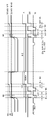
[패널의 구성][Configuration of Panel]
도 7은 도 5에 도시된 표시 장치에 포함되는 패널의 구성을 나타내는 모식적 인 평면도 및 단면도이다. 도면에 도시된 바와 같이, 패널(0)의 중앙에 화면부(화소 어레이부)(1)가 배치되어 있다. 도시되지 않지만 화면부(1)를 둘러싸는 패널(0)의 주변부(프레임부)에 드라이버 및 스캐너 등을 포함하는 구동부가 탑재된다. 그러나, 본 발명은 상기에 한정되는 것이 아니고, 구동부는 패널(0)과 별개로 제공될 수 있다.FIG. 7 is a schematic plan view and a cross-sectional view illustrating a configuration of a panel included in the display device illustrated in FIG. 5. As shown in the figure, a screen portion (pixel array portion) 1 is arranged in the center of the
화면부(1)는 복수의 영역(1A)으로 구획된다. 각각의 영역들(1A)에 대응하도록 광 센서(8)가 배치된다. 광 센서(8)는 대응하는 영역(1A)에 속하는 화소들(2)의 발광 휘도를 검출하여 대응하는 휘도 신호들을 신호 처리부(도시하지 않음)에 공급한다.The
도시된 예에서, 15행×20열의 행렬 형상으로 화소들이 배치된다. 화소 어레이는 12개의 영역으로 구획된다. 각각의 영역(1A)은 5행×5열의 25개의 화소들(2)을 포함한다. 25개의 화소들(2)에 대하여 1개의 광 센서(8)가 배치된다. 1개의 화소(2)에 대해 1개의 광 센서(8)가 형성되는 경우에 비해, 광 센서(8)의 필요한 개수는 대폭 감소될 수 있다.In the example shown, pixels are arranged in a matrix form of 15 rows x 20 columns. The pixel array is divided into 12 regions. Each
[패널의 단면 구조][Section structure of panel]
도 8은 도 7에 도시된 패널의 단면 구조를 나타낸다. 패널(0)은 하부 글래스 기판(101) 및 상부 글래스 기판(108)이 적층되어 있는 구조를 갖는다. 집적 회로(102)는 TFT 프로세스에 의해 글래스 기판(101) 위에 형성된다. 집적 회로(102)는 도 2에 도시된 화소 회로들의 집합이다. 집적 회로(102) 상의 발광 소자 EL의 애노드들(103)은 각각의 화소에 개별적으로 형성된다. 각각의 애노드들(103)을 집 적 회로(102)측에 접속하기 위한 배선들(106)도 형성된다. 애노드들(103) 위에 유기 EL 재료 등으로 구성된 발광층(104)이 형성된다. 그 위에 캐소드(105)가 전면에 걸쳐 형성된다. 캐소드(105), 애노드(103) 및 그 둘 사이에 위치된 발광층(104)은 발광 소자를 구성한다. 캐소드(105) 위에, 밀봉층(107)을 개재하여 글래스 기판(108)이 본딩된다.FIG. 8 shows a cross-sectional structure of the panel shown in FIG. 7. The
유기 EL 발광 소자는 자발광 장치이다. 발광은 대부분 패널(0)의 표면 방향(상부 글래스 기판(108)의 방향)으로 향한다. 그러나, 비스듬히 발광되는 광 및 패널(0)의 내부에서 반복적으로 반사 및 산란되어, 패널(0)의 이면측(하부 글래스 기판(101)의 방향)으로 관통하는 광이 존재한다. 도 5에 도시된 예에서, 광 센서는 패널(0)의 이면 상에 탑재되고, 발광 소자로부터 패널(0)의 이면측으로 관통하는 발광을 검출한다. 이 경우, 광 센서 바로 위의 화소로부터의 발광뿐만 아니라 그 센서 바로 위 위치로부터 시프트된 주변 화소들의 발광 휘도도 측정될 수 있다.The organic EL light emitting element is a self-luminous device. The light emission is mostly directed in the surface direction of the panel 0 (in the direction of the upper glass substrate 108). However, there is light that is emitted at an angle and light that is repeatedly reflected and scattered inside the
[광 센서의 수광량 분포][Received Light Distribution of Light Sensor]
도 9는 광 센서의 수광량 분포를 나타내는 그래프를 도시한다. 도 9의 (X)는 행 방향의 수광 분포를 나타낸다. 횡축은 광 센서로부터의 거리를 화소들의 수로 나타내고, 종축은 센서 출력 전압을 나타낸다. 센서 출력 전압은 수광량에 비례한다. 그래프로부터 명백해진 바와 같이, 광 센서는 그 중심에 위치되는 화소(센서의 바로 위에 위치되는 화소)로부터의 발광뿐만아니라, 그 중심으로부터 떨어진 화소로부터의 발광도 어느 정도 수광하고, 대응하는 휘도 신호들을 출력한다.9 shows a graph showing the light receiving amount distribution of the optical sensor. 9 (X) shows the light receiving distribution in the row direction. The horizontal axis represents the distance from the optical sensor in number of pixels, and the vertical axis represents the sensor output voltage. The sensor output voltage is proportional to the amount of light received. As is evident from the graph, the optical sensor receives not only light emission from a pixel located at its center (a pixel located directly above the sensor), but also a light emission from a pixel away from its center and receives corresponding luminance signals. Output
도 9의 (Y)는 광 센서의 열 방향을 따른 수광량 분포를 나타내고 있다. 도 9의 (X)에 도시된 행 방향의 수광량 분포와 동일한 방식으로, 열 방향에 대해서도 중심 화소로부터의 발광뿐만 아니라 주변 화소로부터의 발광을 어느 정도 수광하고, 대응하는 휘도 신호를 출력할 수 있음을 알게 된다.9 (Y) shows the light receiving amount distribution along the column direction of the optical sensor. In the same manner as the light-receiving amount distribution in the row direction shown in Fig. 9X, not only light emission from the center pixel but also light emission from peripheral pixels can be received to some extent in the column direction, and a corresponding luminance signal can be output. Get to know
본 발명의 실시예에서, 광 센서의 수광량 분포가 영역에서 어느 정도의 폭을 갖는 다는 사실을 이용함으로써, 복수의 화소에 대하여 1개의 광 센서가 배치된다. 따라서, 광 센서들의 수 감소시킬 수 있고, 번인 보정 시스템의 비용을 대폭 삭감할 수 있다. 도 9에 도시된 광 센서의 수광량 분포(수광 강도 분포)를 고려하면, 1개의 광 센서에 의해 측정되는 범위(영역)는 그 광 센서에 대한 거리가 상하 좌우 모든 방향으로 균등한 범위인 것이 바람직하다. 즉, 광 센서는 각각의 구획화된 영역의 중심에 배치되는 것이 바람직하다.In the embodiment of the present invention, by utilizing the fact that the light-receiving amount distribution of the optical sensor has a certain width in the region, one optical sensor is arranged for the plurality of pixels. Thus, the number of optical sensors can be reduced, and the cost of the burn-in correction system can be greatly reduced. In consideration of the light receiving amount distribution (light receiving intensity distribution) of the optical sensor shown in FIG. 9, it is preferable that the range (area) measured by one optical sensor is a range in which the distance to the optical sensor is equal in all directions in the up, down, left, and right directions. Do. That is, the optical sensor is preferably disposed at the center of each partitioned area.
[발광 휘도의 검출 동작][Detection Operation of Luminance Luminance]
도 10은 화소 휘도의 검출 동작을 나타내는 모식도이다. 도면에 도시된 바와 같이, 본 실시예에서 각각의 화소의 발광 휘도는 점 순차 방식에 의해 검출된다. 점 순차 동작의 진행 방향으로서, 각각의 영역(1A)에 좌측 상부의 화소로부터 우측 하부의 화소까지 래스터(Raster) 방식이 사용된다.10 is a schematic diagram illustrating a detection operation of pixel brightness. As shown in the figure, in this embodiment, the light emission luminance of each pixel is detected by the point sequential method. As the advancing direction of the point sequential operation, a raster method is used in each
최초 프레임 1에서 영역(1A)의 좌측 상부에 위치되는 화소(2)가 발광되도록 하는 한편, 영역(1A)에 속하는 모든 나머지 화소들(2)은 비발광 상태가 되도록 한다. 이에 의해, 영역(1A)의 중심에 위치되는 광 센서(8)는 영역(1A)의 좌측 상부 코너(corner)에 위치되는 화소(2)의 발광 휘도를 검출할 수 있다.In the
다음 프레임 2로 진행하면, 좌측 상부로부터 2번째 위치의 화소(2)만이 발광 하고, 그 휘도가 검출된다. 그 후, 동작이 순차적으로 진행하여, 프레임 5에서 우상부 코너에 위치되는 화소(2)의 발광 휘도가 검출될 수 있다. 계속해서 프레임 6에서, 2번째 줄의 화소의 발광 휘도가 검출되고, 이 후 프레임 7로부터 순서대로 프레임 10으로 프로세스가 진행한다. 프레임 10에서, 위에서 2번째 줄째의 우측 단부에 위치되는 화소(2)의 발광 휘도가 검출될 수 있다. 따라서, 프레임 1로부터 프레임 25까지 영역(1A)에 속하는 25개의 화소(2)의 발광 휘도가 점 순차 방식으로 검출될 수 있다. 예를 들어, 프레임 주파수가 30Hz이면, 영역(1A)에 속하는 모든 화소들(2)의 발광 휘도는 약 1초 이하 동안 검출될 수 있다. 점 순차 방법은 모든 영역(1A)에서 병렬로 행해지고, 전체 패널의 발광 휘도는 1초 이하 동안 검출될 수 있다. 상기 설명으로부터 명백해진 바와 같이, 본 실시예에서 1개의 광 센서(8)에 의해 수광 가능한 영역(1A)에 포함되는 화소들(2)은 1 화소씩 점 순차 방식으로 발광된다. 컬러 표시 장치의 경우, 1 화소에 포함되는 발광 소자는 RGB 중 임의의 광을 발광한다. 이 경우, 각각의 색에 대한 각각의 화소(서브 화소)에서의 발광 휘도가 검출되는 것이 바람직하다. RGB의 3색의 서브 화소들이 서로 결합되는 화소에 대한 발광 휘도를 검출하는 것도 때때로 가능하다. 점 순차 검출에 있어서의 각각의 화소의 발광 제어는 패널(0)에 입력되는 영상 신호에 의해 행해지고, 화소의 동작 타이밍은 통상의 화상 표시와 동일한 방식으로 행해진다. 즉, 신호 처리부는 각각의 프레임에 검출용 영상 신호를 공급한다. 검출용 영상 신호는 검출 대상의 화소들만이 1 프레임에서 발광하도록 하고, 나머지 화소들은 비발광의 상태가 되도록 한다. 점 순차 주사에 의해, 복수의 화소들의 휘도 데이터가 1개의 광 센 서에 의해 순차적으로 획득될 수 있다.Proceeding to the
[번인 현상][Burn-in phenomenon]
도 11은 본 발명의 실시예의 처리 대상으로서의 "번인"을 설명하는 모식도이다. (A1)은 번인의 원인으로서의 패턴 표시를 나타낸다. 예를 들어, 도시된 바와 같은 윈도우가 화면부(1)에 표시된다. 흰 부분 윈도우의 부분의 화소들은 고 휘도로 발광을 지속하는 한편, 주변의 블랙 프레임 부분의 화소들은 비발광 상태에 놓인다. 이러한 윈도우 패턴이 장시간에 걸쳐서 표시되면, 흰 부분의 화소들의 휘도 저하가 진행되는 한편, 블랙 프레임 부분의 화소들의 휘도 저하는 상대적으로 느리게 진행한다.It is a schematic diagram explaining "burn in" as a process target of the Example of this invention. (A1) shows pattern display as a cause of burn-in. For example, a window as shown is displayed on the
(A2)는 (A1)에 도시된 윈도우 패턴 표시를 소거되고, 전면 래스터 표시가 화면부(1)에 행해지는 상태를 나타낸다. 부분적인 휘도 저하가 없다면, 화면부(1)에 래스터 표시가 행해질 때, 전체 화면에서 균일한 휘도 분포가 얻어질 수 있다. 그러나, 실제로는 이전에 흰 부분으로 표시된 중앙 부분의 화소들의 휘도 저하가 진행하고 있기 때문에, 중앙 부분의 휘도는 주변 부분의 휘도보다 낮아져, 도면에 도시된 바와 같이 "번인"이 나타난다.(A2) erases the window pattern display shown in (A1), and shows a state in which the front raster display is performed on the
[번인 보정 처리][Burn In Correction Processing]
도 12는 도 11에 도시된 "번인"의 보정 동작을 나타내는 모식도이다. (O)은 외부로부터 표시 장치의 신호 처리부에 입력되는 영상 신호를 나타내고 있다. 예에서, 전면 영상 신호가 도시된다.FIG. 12 is a schematic diagram showing a correction operation of "burn in" shown in FIG. (O) shows a video signal input to the signal processing unit of the display device from the outside. In the example, the front image signal is shown.
(A)는 도 11에 도시된 바와 같은 "번인"이 이미 발생하고 있는 화면부에 (O) 에 도시된 영상 신호를 표시한 경우의 휘도 분포를 나타내고 있다. 전면 영상 신호가 입력될 때도, 패널의 화면부에 부분적인 번인이 존재하여, 중앙의 윈도우 부분의 휘도가 주변 프레임 부분보다 어둡다.(A) shows the luminance distribution in the case where the video signal shown in (O) is displayed on the screen portion where "burn-in" has already occurred as shown in FIG. Even when the front image signal is input, partial burn-in exists in the screen portion of the panel, so that the luminance of the center window portion is darker than the peripheral frame portion.
(B)는 외부로부터 입력된 영상 신호 (O)을 각각의 화소들의 발광 휘도의 검출 결과에 따라 보정함으로써 획득된 영상 신호를 나타낸다. (B)에 도시된 번인 보정 후의 영상 신호에서, 중앙의 윈도우 부분의 화소들에 기입되는 영상 신호의 레벨은 상대적으로 높게 보정되고, 주변 프레임 부분의 화소들에 기입되는 영상 신호의 레벨은 상대적으로 낮게 보정된다. 상술된 바와 같이, 영상 신호가 (A)에 도시된 번인에 의한 부(negative) 휘도 분포를 상쇄(cancel)시키기 위해, (B)에 도시된 정(positive) 휘도 분포를 갖도록 보정이 행해진다.(B) shows the image signal obtained by correcting the image signal O input from the outside according to the detection result of the light emission luminance of each pixel. In the video signal after burn-in correction shown in (B), the level of the video signal written in the pixels of the center window portion is corrected relatively high, and the level of the video signal written in the pixels of the peripheral frame portion is relatively high. The correction is low. As described above, in order to cancel the negative luminance distribution due to burn-in shown in (A), correction is performed to have a positive luminance distribution shown in (B).
(C)는 번인 보정 후의 영상 신호가 화면부에 표시된 상태를 모식적으로 나타낸다. 패널의 화면부에 남아있는 번인으로 인한 불균일한 휘도 분포는 번인 보정용 영상 신호에 의해 보상되어, 균일한 휘도 분포를 갖는 화면이 얻어질 수 있다.(C) schematically shows a state where the video signal after burn-in correction is displayed on the screen portion. Uneven luminance distribution due to burn-in remaining in the screen portion of the panel is compensated by the burn-in correction image signal, so that a screen having a uniform luminance distribution can be obtained.
<제2 실시예>Second Embodiment
[휘도 신호들의 동적 범위][Dynamic Range of Luminance Signals]
도 13은 광 센서로부터 출력되는 휘도 신호들의 동적 범위를 나타내는 그래프이다. 횡축은 광 센서의 중심 위치로부터의 거리에 대한 것이고, 종축은 휘도 신호의 출력 전압에 대한 것이다. 횡축의 거리는 광 센서로부터의 화소들의 수로 나타나 있다. 도면에 도시된 바와 같이, 광 센서로부터 거리가 멀어짐에 따라, 화소 휘도가 동일한 경우에도, 광 센서에 의한 수광값은 감소된다. 도시된 예에서, 중심 위치의 화소의 휘도 신호의 출력 레벨은 3V에 도달하는 한편, 중심 위치로부터 화소들의 수로 20개 화소만큼 떨어진 화소의 휘도 신호의 출력 전압은 약 1/10인 0.3V까지 저하된다. 도 5에 도시된 번인 보정 시스템에서, 광 센서(8)로부터의 출력이 증폭된 후, 아날로그 신호가 ADC(9)에 의해 디지털 신호로 변환된다. 디지털 신호의 비트는 입력 아날로그 신호의 최대 전압을 고려하여 결정될 수 있다. 따라서, 광 센서의 중심에 위치되는 화소에서, 휘도 신호는 예를 들어, 8비트의 256 계조에서 변환될 수 있다. 따라서, 번인 보정의 정밀도가 증가된다. 한편, 광 센서로부터 떨어진 화소에서, 아날로그 신호의 전압은 26 계조 레벨에서 변환된다. 따라서, 번인 보정의 정밀도가 감소된다. 결과로서, 번인 보정이 충분히 행해지지 않을 우려가 있다. 도시의 예에서, 중심에 위치되는 화소의 휘도 신호의 동적 범위가 크기 때문에, 신호는 256 계조의 디지털 데이터로 변환될 수 있다. 이것은 0.4%의 보정 정밀도에 대응한다. 한편, 중심으로부터 20개 화소들만큼 떨어진 화소의 휘도 신호의 동적 범위는 좁기 때문에, 신호는 단지 26 계조 내에서 변환된다. 이것은 4%의 보정 정밀도에 대응한다.13 is a graph illustrating a dynamic range of luminance signals output from an optical sensor. The horizontal axis is for the distance from the center position of the optical sensor, and the vertical axis is for the output voltage of the luminance signal. The distance along the horizontal axis is represented by the number of pixels from the light sensor. As shown in the figure, as the distance from the optical sensor increases, the light reception value by the optical sensor decreases even when the pixel luminance is the same. In the example shown, the output level of the luminance signal of the pixel at the center position reaches 3V, while the output voltage of the luminance signal of the
[제2 실시예의 동작들][Operations of Second Embodiment]
도 14a는 제2 실시예에 따른 표시 장치의 동작들을 나타내는 타이밍 차트이다. 제2 실시예에서, 상술된 번인 보정의 정밀도의 편차를 향상시킴으로써 번인 보정의 정밀도가 증가된다. 도 14a는 측정 대상의 화소들만을 점등하기 위한 점 순차 주사를 나타낸다. 상술된 바와 같이, 점 순차 주사는 도 3에 도시된 통상의 영상 표시 동작의 시퀀스와 동일한 시퀀스에서 행해진다. 즉, Vth 보정이 행해진 후, 소정 레벨의 영상 신호가 측정 대상의 화소에 기입되고, 이동도 보정이 행해져 화소가 발광된다.14A is a timing chart illustrating operations of the display device according to the second embodiment. In the second embodiment, the accuracy of the burn-in correction is increased by improving the deviation of the precision of the burn-in correction described above. 14A shows dot sequential scanning for lighting only pixels of a measurement object. As described above, dot sequential scanning is performed in the same sequence as that of the normal video display operation shown in FIG. That is, after Vth correction is performed, a video signal having a predetermined level is written into the pixel to be measured, and mobility correction is performed to emit light.
도 14a에 도시된 타이밍 차트는 측정 대상의 화소가 광 센서에 가까운 경우를 나타낸다. 이 경우에, 광 센서는 측정 대상의 화소로부터 충분한 수광량을 얻을 수 있다. 따라서, 1 프레임에 할당된 발광 기간은 비교적 짧을 수 있다. 따라서, 도 14a에 도시된 타이밍 차트에서, 화소가 발광한 후, 급전선 VL은 비교적 짧은 시간 폭에서 고 레벨 Vdd로부터 저 레벨 Vss로 전환되어, 비발광 기간으로 진행한다.The timing chart shown in FIG. 14A shows the case where the pixel to be measured is close to the optical sensor. In this case, the optical sensor can obtain a sufficient light receiving amount from the pixel to be measured. Therefore, the light emission period allocated to one frame can be relatively short. Therefore, in the timing chart shown in Fig. 14A, after the pixel emits light, the feed line VL is switched from the high level Vdd to the low level Vss in a relatively short time width, and proceeds to the non-light emitting period.
도 14b 또한 제2 실시예에 따른 표시 장치의 동작들을 설명하기 위한 타이밍 차트이다. 이해를 쉽게 하기 위해서, 도 14a에 도시된 타이밍 차트에 사용된 동일한 부호가 적용된다. 챠트는 발광 휘도의 측정 대상의 화소가 광 센서로부터 비교적 떨어져 위치된 경우를 나타낸다. 이 경우, 측정 대상의 화소의 발광 기간은 비교적 길게 된다. 이에 의해, 광 센서는 측정 대상의 화소로부터 충분한 수광량을 얻을 수 있다.14B is a timing chart for describing operations of the display device according to the second embodiment. For ease of understanding, the same signs used in the timing chart shown in Fig. 14A are applied. The chart shows a case where the pixel to be measured for the light emission luminance is located relatively far from the optical sensor. In this case, the light emission period of the pixel to be measured becomes relatively long. Thereby, the optical sensor can obtain sufficient light reception amount from the pixel of a measurement object.
상술된 바와 같이, 본 실시예에 따르면, 신호 처리부는 측정 대상의 화소와 그 화소의 발광 휘도를 검출하는 광 센서 사이의 거리에 따라, 1 프레임에서 화소가 차지하는 발광 기간의 비율을 설정한다. 이에 의해, 화소가 광 센서로부터 떨어진 만큼 광 센서가 수광하는 시간이 길어진다.As described above, according to the present embodiment, the signal processing unit sets the ratio of the light emission period occupied by the pixel in one frame according to the distance between the pixel to be measured and the optical sensor for detecting the light emission luminance of the pixel. This increases the time that the optical sensor receives the light as the pixel is separated from the optical sensor.
[휘도 신호의 출력분포][Output distribution of luminance signal]
도 15는 제2 실시예에서 얻어지는 휘도 신호의 출력 전압 분포를 나타내는 그래프이다. 이해를 쉽게 하기 위해, 도 13에 도시된 그래프와 동일한 표기가 적용된다. 광 센서로부터의 거리와 발광 시간 사이의 관계가 최적이 되도록 설정되는 경우, 도 15의 그래프에 도시된 바와 같이, 광 센서의 출력 전압은 화소의 위치에 관계없이 일정할 것이다. 즉, 광 센서로부터의 거리에 관계없이 휘도 신호들의 레벨들을 각각의 화소들에서 일정하게 하기 위해서, 광 센서에 가까운 화소는 도 14a에 도시된 바와 같이 짧은 듀티(short duty)의 타이밍으로 발광하게 된다. 반면, 광 센서로부터 떨어진 화소는 도 14b에 도시된 바와 같이 긴 듀티의 타이밍으로 발광하게 된다. 따라서, 각각의 화소들에서 일정한 동적 범위는, 도 15에 도시된 바와 같이 광 센서로부터의 거리에 관계없이 광 센서에 의해 얻어지는 발광 휘도 데이터에서 얻어질 수 있다. 도시된 예에서, 모든 화소에서 256 계조의 해상도가 얻어질 수 있고, 0.4%의 정밀도로 번인 보정이 행해질 수 있다. 보정 시스템에 포함된 AD 컨버터는, 광 센서로부터의 거리에 관계없이 모든 화소에 대하여 동일한 계조의 정밀도(예를 들어, 도시된 예에서는 8비트, 256 계조)로 디지털 변환을 행할 수 있다. 그 결과, 휘도 저하를 측정하기 위한 데이터 정밀도도 증가될 수 있고, 높은 정밀도의 휘도 보정이 행해질 수도 있다.15 is a graph showing the output voltage distribution of the luminance signal obtained in the second embodiment. For ease of understanding, the same notation as in the graph shown in FIG. 13 is applied. When the relationship between the distance from the light sensor and the light emission time is set to be optimal, as shown in the graph of FIG. 15, the output voltage of the light sensor will be constant regardless of the position of the pixel. That is, in order to make the levels of the luminance signals constant in the respective pixels irrespective of the distance from the optical sensor, the pixels close to the optical sensor emit light at a short duty timing as shown in FIG. 14A. . On the other hand, the pixel away from the light sensor emits light at a long duty timing as shown in FIG. 14B. Thus, a constant dynamic range in each of the pixels can be obtained from the luminescence brightness data obtained by the optical sensor irrespective of the distance from the optical sensor as shown in FIG. In the example shown, 256 gradations of resolution can be obtained in all pixels, and burn-in correction can be performed with an accuracy of 0.4%. The AD converter included in the correction system can perform digital conversion with the same gradation precision (for example, 8 bits, 256 gradations in the illustrated example) for all pixels regardless of the distance from the optical sensor. As a result, the data precision for measuring the luminance decrease can also be increased, and a high precision luminance correction can be performed.
<제3 실시예>Third Embodiment
[발광 휘도 검출의 타이밍 차트][Timing chart of emission luminance detection]
도 16a는 본 발명의 제3 실시예에 따른 타이밍 차트이다. 차트는 화소의 발광 휘도를 검출하기 위한 점 순차 동작을 나타낸다. 타이밍 차트는 측정 대상의 화소가 광 센서에 가깝게 위치된 경우를 나타낸다. 도면에 도시된 바와 같이, 낮 은 신호 전압의 영상 신호가 광 센서에 가까운 화소에 기입된다.16A is a timing chart according to a third embodiment of the present invention. The chart shows the point sequential operation for detecting the light emission luminance of the pixel. The timing chart shows a case where the pixel to be measured is located close to the optical sensor. As shown in the figure, an image signal of a low signal voltage is written in a pixel close to the optical sensor.
도 16b 또한 제3 실시예에 따른 타이밍 차트이다. 그 차트는, 챠트가 광 센서로부터 떨어져 위치된 화소에 대한 발광 휘도의 검출 동작을 나타낸다는 점에서 도 16a와 상이하다. 도면에 도시된 바와 같이, 높은 신호 전압의 영상 신호가 광 센서로부터 떨어진 화소에 기입된다. 따라서, 영상 신호의 레벨이 광 센서로부터의 거리에 따라 최적이 되도록 설정되면, 각각의 화소들의 발광 휘도 데이터는 광 센서로부터의 거리에 관계없이 일정한 값을 유지할 수 있다. 즉, 본 실시예에 따른 신호 처리부는 검출 대상의 화소와 그 화소의 발광 휘도를 검출하는 광 센서 사이의 거리에 따라 화소에 기입될 검출용 영상 신호의 레벨을 설정한다. 그 결과, 화소가 광 센서로부터 떨어짐에 따라 발광 휘도가 증가된다. 증폭 후의 AD 컨버터 에 입력된 신호 레벨도 광 센서로부터의 거리에 관계없이 일정한 값일 것이다. 모든 화소에 대하여 동일한 계조의 정밀도(예를 들어, 8비트, 256 계조)로 디지털 변환이 행해질 수 있다. 그 결과, 휘도 저하의 데이터 정밀도를 증가시킬 수 있고, 높은 정밀도의 휘도 보정을 실현할 수 있다.16B is also a timing chart according to the third embodiment. The chart is different from FIG. 16A in that the chart shows the detection operation of the luminescence brightness with respect to the pixel located away from the optical sensor. As shown in the figure, an image signal of a high signal voltage is written in a pixel away from the optical sensor. Therefore, when the level of the image signal is set to be optimal according to the distance from the optical sensor, the emission luminance data of each pixel can maintain a constant value regardless of the distance from the optical sensor. That is, the signal processing unit according to the present embodiment sets the level of the detection video signal to be written in the pixel according to the distance between the pixel to be detected and the optical sensor for detecting the light emission luminance of the pixel. As a result, the light emission luminance increases as the pixel is separated from the optical sensor. The signal level input to the AD converter after amplification will also be a constant value regardless of the distance from the optical sensor. Digital conversion can be performed for all the pixels with the same gradation precision (for example, 8 bits, 256 gradations). As a result, the data precision of luminance fall can be increased, and high precision luminance correction can be realized.
본 실시예에서는, 신호 전압의 레벨에 의해 휘도가 제어됨으로써, 제2 실시예와 같이 패널을 구동하는 타이밍을 변화시키지 않고 발광 휘도의 검출 동작을 행한다. 따라서, 본 실시예의 동작은 통상의 영상 표시 시의 동작과 비교하여 신호 전압만이 변화되는 동작일 것이고, 따라서, 발광 휘도 검출 시에 새로운 타이밍을 설정할 필요가 없어, 시스템을 간소화한다.In this embodiment, the luminance is controlled by the level of the signal voltage, so that the light emission luminance detection operation is performed without changing the timing of driving the panel as in the second embodiment. Therefore, the operation of the present embodiment will be an operation in which only the signal voltage is changed as compared with the operation in normal video display, and therefore, it is not necessary to set a new timing at the time of detecting the light emission luminance, thereby simplifying the system.
<제4 실시예><Fourth Embodiment>
[패널 구성]Panel Configuration
도 17은 본 발명의 제4 실시예에 따른 표시 장치의 패널 구성을 나타내는 블록도이다. 이해를 쉽게 하기 위해, 도 1에 도시된 제1 실시예의 패널 블록도와 동일한 부호가 적용된다. 본 표시 장치는 기본적으로 화소 어레이부(화면부)(1) 및 화소 어레이부를 구동하는 구동부를 포함한다. 화소 어레이부(1)는 제1 주사선들의 행들 WS, 마찬가지로 제2 주사선들의 행들 DS, 신호선들의 열들 SL 및 각각의 제1 주사선들 WS 및 각각의 신호선들 SL이 교차하는 부분에 배치된 행렬 형상의 화소들(2)을 포함한다. 반면, 구동부는 기입 스캐너(4), 구동 스캐너(5) 및 수평 선택기(3)를 포함한다. 기입 스캐너(4)는 각각의 제1 주사선 WS에 제어 신호를 출력함으로써 화소들(2)의 선 순차 주사를 행 단위로 행한다. 구동 스캐너(5)도 각각의 제2 주사선 DS에 제어 신호를 출력함으로써 화소들(2)의 선 순차 주사를 행 단위로 행한다. 제어 신호가 출력되는 타이밍은 기입 스캐너(4) 및 구동 스캐너(5)에서 상이하다. 구동 스캐너(5)는 제1 실시예에서 사용된 전원 스캐너(6) 대신에 구동부에 배치된다. 전원 스캐너가 제거되기 때문에, 급전선도 화소 어레이부(1)로부터 제거된다. 그 대신, 고정 전원 전위 Vdd(도시되지 않음)를 공급하는 전원 라인이 화소 어레이부(1)에 제공된다. 수평 선택기(신호 드라이버)(3)는 스캐너들(4 및 5)의 선 순차 주사에 대응하도록, 신호선들의 열들 SL에 영상 신호의 신호 전압 및 기준 전압을 공급한다.17 is a block diagram illustrating a panel configuration of a display device according to a fourth exemplary embodiment of the present invention. For ease of understanding, the same reference numerals apply to the panel block diagram of the first embodiment shown in FIG. The display device basically includes a pixel array portion (screen portion) 1 and a driving portion for driving the pixel array portion. The
[화소 회로의 구성][Configuration of Pixel Circuit]
도 18은 도 17에 도시된 제4 실시예의 표시 패널에 포함되는 화소 회로의 구 성을 나타낸다. 제1 실시예의 화소 회로는 2개의 트랜지스터들을 포함하는 한편, 본 실시예의 화소는 3개의 트랜지스터를 포함한다. 도면에 도시된 바와 같이, 본 화소(2)는 기본적으로 발광 소자 EL, 샘플링 트랜지스터 Tr1, 구동 트랜지스터 Trd, 스위칭 트랜지스터 Tr3 및 화소 용량 소자 Cs를 포함한다. 샘플링 트랜지스터 Tr1은 그의 제어 단부(게이트)가 주사선 WS에 접속되고, 한 쌍의 전류 단부들(소스/드레인)의 한쪽은 신호선 SL에 접속되며, 전류 단부들의 다른 쪽은 구동 트랜지스터 Trd의 제어 단부(게이트 G)에 접속된다. 구동 트랜지스터 Trd는 한 쌍의 전류 단부들(소스/드레인)의 한쪽(드레인)은 전원 라인 Vdd에 접속되고, 전류 단부들의 다른 쪽(소스 S)은 발광 소자 EL의 애노드에 접속된다. 발광 소자 EL의 캐소드는 소정의 캐소드 전위 Vcath에 접속된다. 스위칭 트랜지스터 Tr3은 그의 제어 단부(게이트)가 주사선 DS에 접속되고, 한 쌍의 전류 단부들(소스/드레인)의 한쪽은 고정 전위Vss에 접속되며, 전류 단부들의 다른 쪽은 구동 트랜지스터 Trd의 소스 S에 접속된다. 화소 용량 소자 Cs는 그 일단부가 구동 트랜지스터 Trd의 제어 단부(게이트 G)에 접속되고, 그의 타단이 구동 트랜지스터 Trd의 다른 쪽의 전류 단부(소스 S)에 접속된다. 구동 트랜지스터 Trd의 다른 쪽의 전류 단부는 발광 소자 EL 및 화소 용량 소자 Cs에 대한 출력 전류 단부이다. 본 화소 회로(2)에서, 화소 용량 소자 Cs를 보조하기 위해, 보조 용량 소자 Csub가 구동 트랜지스터 Trd의 소스 S와 전원 Vdd 사이에 접속된다.FIG. 18 illustrates a configuration of a pixel circuit included in the display panel of the fourth exemplary embodiment shown in FIG. 17. The pixel circuit of the first embodiment includes two transistors, while the pixel of this embodiment includes three transistors. As shown in the figure, this
상기 구성에서, 구동부측의 기입 스캐너(4)는 샘플링 트랜지스터 Tr1의 스위칭 제어를 행하기 위한 제어 신호를 제1 주사선 WS에 공급한다. 구동 스캐너(5)는 스위칭 트랜지스터 Tr3의 스위칭 제어를 행하기 위한 제어 신호를 제2 주사선 DS에 출력한다. 수평 선택기(3)는 신호 전위 Vsig와 기준 전위 Vref 사이에서 전환되는 영상 신호(입력 신호)를 신호선 SL에 공급한다. 상술된 바와 같이 주사선들 WS, DS 및 신호선들 SL의 전위가 선 순차 주사에 따라 변화하지만, 전원 라인은 Vdd에 고정되어 있다. 캐소드 전위 Vcath 및 고정 전위 Vss도 일정하다.In the above configuration, the
[화소 회로의 동작][Operation of Pixel Circuit]
도 19는 도 18에 도시된 화소 회로의 동작들을 설명하기 위한 타이밍 차트이다. 도면에 도시된 바와 같이, 주사선 WS, 주사선 DS 및 신호선 SL의 전위 변화는 이러한 선들에 대해 시간축을 공통으로 하여 나타나 있다. 샘플링 트랜지스터 Tr1은 N 채널형이며, 주사선 WS가 하이 레벨에 있는 경우에 턴온된다. 스위칭 트랜지스터 Tr3도 N 채널형이며, 주사선 DS가 하이 레벨에 있는 경우에 턴온된다. 한편, 신호선 SL에 공급된 영상 신호는 1 수평 주기(1H)로 신호 전위 Vsig과 기준 전위 Vref 사이에서 전환된다. 타이밍 차트는, 시간축이 제1 주사선 WS, 제2 주사선 DS 및 신호선 SL의 전위 변화에 대응하도록, 구동 트랜지스터 Trd의 게이트 G 및 소스 S의 전위 변화를 나타낸다. 게이트 G와 소스 S 사이의 전위차 Vgs에 따라 구동 트랜지스터 Trd의 동작 상태가 제어된다.FIG. 19 is a timing chart for describing operations of the pixel circuit shown in FIG. 18. As shown in the figure, the potential change of the scan line WS, the scan line DS and the signal line SL is shown with the time axis in common for these lines. The sampling transistor Tr1 is of N channel type and is turned on when the scanning line WS is at the high level. The switching transistor Tr3 is also N channel type and is turned on when the scanning line DS is at a high level. On the other hand, the video signal supplied to the signal line SL is switched between the signal potential Vsig and the reference potential Vref in one horizontal period 1H. The timing chart shows the potential change of the gate G and the source S of the drive transistor Trd so that the time axis corresponds to the potential change of the first scan line WS, the second scan line DS, and the signal line SL. The operating state of the driving transistor Trd is controlled in accordance with the potential difference Vgs between the gate G and the source S.
우선, 화소가 이전 프레임의 발광 기간으로부터 비발광 기간으로 진입되면, 타이밍 T1에서 주사선 DS가 하이 레벨로 전환되고, 스위칭 트랜지스터 Tr3은 턴온된다. 이에 의해, 구동 트랜지스터 Trd의 소스 S의 전위는 고정 전위 Vss로 설정된다. 이때, 고정 전위 Vss는 발광 소자 EL의 임계 전압 Vthel과 캐소드 전위 Vcath의 합보다도 작게 설정된다. 즉, 고정 전위 Vss는 Vss<Vthel+Vcath로 설정되되고, 발광 소자 EL은 역 바이어스 상태에 있으며, 따라서, 구동 전류 Ids는 발광 소자 EL에 흐르지 않는다. 그러나, 구동 트랜지스터 Trd로부터 공급된 출력 전류 Ids는 소스 S를 통해 고정 전위 Vss에 흐른다.First, when the pixel enters the non-emission period from the light emission period of the previous frame, the scanning line DS is switched to the high level at timing T1, and the switching transistor Tr3 is turned on. Thereby, the potential of the source S of the drive transistor Trd is set to the fixed potential Vss. At this time, the fixed potential Vss is set smaller than the sum of the threshold voltage Vthel and the cathode potential Vcath of the light emitting element EL. That is, the fixed potential Vss is set to Vss < Vthel + Vcath, and the light emitting element EL is in a reverse biased state, and therefore the driving current Ids does not flow through the light emitting element EL. However, the output current Ids supplied from the drive transistor Trd flows through the source S to the fixed potential Vss.
계속해서, 타이밍 T2에서, 샘플링 트랜지스터 Tr1은 신호선 SL의 전위가 Vref에 있는 상태에서 턴온된다. 이에 의해, 구동 트랜지스터 Trd의 게이트 G는 기준 전위 Vref로 설정된다. 이에 의해, 구동 트랜지스터 Trd의 게이트 G와 소스 S 사이의 전압 Vgs는 Vref-Vss의 값일 것이다. 여기에서, Vgs는 Vref-Vss>Vth로 설정된다. Vref-Vss가 구동 트랜지스터 Trd의 임계 전압 Vth보다도 크지 않으면, 후속의 임계 전압 보정 동작을 정상적으로 행하는 것은 어렵다. 그러나, Vgs는 Vref-Vss>Vth이므로, 구동 트랜지스터 Trd는 온 상태에 있으며, 드레인 전류는 전원 전위 Vdd로부터 고정 전위 Vss로 흐른다.Subsequently, at timing T2, sampling transistor Tr1 is turned on with the potential of signal line SL at Vref. As a result, the gate G of the driving transistor Trd is set to the reference potential Vref. Thereby, the voltage Vgs between the gate G and the source S of the drive transistor Trd will be the value of Vref-Vss. Here, Vgs is set to Vref-Vss> Vth. If Vref-Vss is not larger than the threshold voltage Vth of the drive transistor Trd, it is difficult to perform the subsequent threshold voltage correction operation normally. However, since Vgs is Vref-Vss> Vth, the driving transistor Trd is in the on state, and the drain current flows from the power supply potential Vdd to the fixed potential Vss.
이 후, 타이밍 T3에서, 동작은, 스위칭 트랜지스터 Tr3이 턴오프되어 구동 트랜지스터 Trd의 소스 S가 고정 전위 Vss로부터 컷오프되는 임계 전압 보정 기간으로 진입된다. 여기에서, 소스 S의 전위(즉, 발광 소자의 애노드 전위)가 캐소드 전위 Vcath에 발광 소자 EL의 임계 전압 Vthel을 더함으로써 획득된 값보다도 낮은 한, 발광 소자 EL은 여전히 역 바이어스 상태에 있고, 약간의 누설 전류만이 흐른다. 따라서, 전원 라인 Vdd로부터 구동 트랜지스터 Trd를 통해 공급되는 대부분의 전류는, 화소 용량 소자 Cs 및 보조 용량 소자 Csub를 충전하는데 사용된다. 이러한 방식으로 화소 용량 소자 Cs가 충전되기 때문에, 구동 트랜지스터 Trd의 소스 전위는 시간에 따라 Vss로부터 증가한다. 일정 기간 이후, 구동 트랜지스터 Trd의 소스 전위는 레벨 Vref-Vth에 도달하고, Vgs는 정확히 Vth가 된다. 이 시점에서, 구동 트랜지스터 Trd가 컷오프되고, Vth에 대응하는 전압이 구동 트랜지스터 Trd의 소스 S와 게이트 G 사이에 배치되는 화소 용량 소자 Cs에 기입된다. 임계 전압 보정 동작이 완료되는 시점에서도, 소스 전압 Vref-Vth는 캐소드 전위 Vcath에 발광 소자의 임계 전압 Vthel을 더함으로써 획득된 값보다도 낮다.Thereafter, at timing T3, the operation enters the threshold voltage correction period in which the switching transistor Tr3 is turned off so that the source S of the driving transistor Trd is cut off from the fixed potential Vss. Here, as long as the potential of the source S (i.e., the anode potential of the light emitting element) is lower than the value obtained by adding the threshold voltage Vthel of the light emitting element EL to the cathode potential Vcath, the light emitting element EL is still in a reverse biased state, and slightly Only leakage current flows. Therefore, most of the current supplied from the power supply line Vdd through the driving transistor Trd is used to charge the pixel capacitor Cs and the storage capacitor Csub. Since the pixel capacitor Cs is charged in this manner, the source potential of the driving transistor Trd increases from Vss with time. After a period of time, the source potential of the driving transistor Trd reaches the level Vref-Vth, and Vgs becomes exactly Vth. At this point, the drive transistor Trd is cut off, and a voltage corresponding to Vth is written to the pixel capacitor Cs disposed between the source S and the gate G of the drive transistor Trd. Even when the threshold voltage correction operation is completed, the source voltage Vref-Vth is lower than the value obtained by adding the threshold voltage Vthel of the light emitting element to the cathode potential Vcath.
계속해서, 타이밍 T4에서, 기입 기간/이동도 보정 기간으로 프로세스가 진행된다. 타이밍 T4에서, 신호선 SL은 기준 전위 Vref로부터 신호 전위 Vsig로 전환된다. 신호 전위 Vsig은 계조에 대응하는 전압이다. 이 시점에서 샘플링 트랜지스터 Tr1은 온 상태에 있기 때문에, 구동 트랜지스터 Trd의 게이트 G의 전위는 Vsig일 것이다. 이에 의해, 구동 트랜지스터 Trd는 턴온되고, 전류가 전원 라인 Vdd로부터 흘러, 소스 S의 전위가 시간에 따라 증가한다. 소스 S의 전위가 발광 소자 EL의 임계 전압 Vthel 및 캐소드 전압 Vcath의 합을 여전히 초과하지 않으므로, 발광 소자 EL에는 약간의 누설 전류만이 흐르며, 구동 트랜지스터 Trd로부터 공급된 대부분의 전류는 화소 용량 소자 Cs 및 보조 용량 소자 Csub를 충전하는데 사용된다. 상술된 바와 같이 충전 프로세스에서 소스 S의 전위가 증가한다.Subsequently, at timing T4, the process proceeds to the writing period / mobility correction period. At the timing T4, the signal line SL is switched from the reference potential Vref to the signal potential Vsig. The signal potential Vsig is a voltage corresponding to the gray scale. At this point, since the sampling transistor Tr1 is in the on state, the potential of the gate G of the driving transistor Trd will be Vsig. As a result, the driving transistor Trd is turned on, a current flows from the power supply line Vdd, and the potential of the source S increases with time. Since the potential of the source S still does not exceed the sum of the threshold voltage Vthel and the cathode voltage Vcath of the light emitting element EL, only a small leakage current flows in the light emitting element EL, and most of the current supplied from the driving transistor Trd is the pixel capacitor Cs. And the storage capacitor Csub. As described above, the potential of the source S increases in the charging process.
기입 기간에 구동 트랜지스터 Trd의 임계 전압 보정 동작이 이미 완료되기 때문에, 구동 트랜지스터 Trd로부터 공급되는 전류는 이동도 μ를 반영한다. 구체적으로, 구동 트랜지스터 Trd의 이동도 μ가 큰 경우, 구동 트랜지스터 Trd에 의해 공급되는 전류량은 커지고, 소스 S의 전위도 빠르게 증가한다. 반면, 이동도 μ가 작은 경우, 구동 트랜지스터 Trd의 전류 공급량은 작고, 소스 S의 전위는 느리게 증가한다. 이러한 방식으로 구동 트랜지스터 Trd의 출력 전류가 화소 용량 소자 Cs에 부귀환되고, 결과적으로, 구동 트랜지스터 Trd의 게이트 G 및 소스 S의 전압 Vgs는 이동도 μ를 반영한 값일 것이고, 전압 Vgs는 일정 시간 경과 후에 이동도 μ가 완전히 보정된 값일 것이다. 즉, 기입 기간에서, 구동 트랜지스터 Trd로부터 흘러 나온 전류를 화소 용량 소자 Cs에 부귀환함으로써, 구동 트랜지스터 Trd의 이동도 μ의 보정이 동시에 행해진다.Since the threshold voltage correction operation of the driving transistor Trd is already completed in the writing period, the current supplied from the driving transistor Trd reflects the mobility µ. Specifically, when the mobility mu of the driving transistor Trd is large, the amount of current supplied by the driving transistor Trd becomes large, and the potential of the source S also rapidly increases. On the other hand, when the mobility μ is small, the current supply amount of the driving transistor Trd is small, and the potential of the source S increases slowly. In this way, the output current of the driving transistor Trd is negatively fed back to the pixel capacitor Cs, and as a result, the voltage Vgs of the gate G and the source S of the driving transistor Trd will be a value reflecting the mobility μ, and the voltage Vgs after a predetermined time has elapsed. The mobility μ will be a fully calibrated value. That is, in the writing period, the current flowing out of the driving transistor Trd is negatively fed back to the pixel capacitor Cs, thereby simultaneously correcting the mobility mu of the driving transistor Trd.
마지막으로, 타이밍 T5에서 프로세스가 현재 프레임의 발광 기간으로 진행되면, 샘플링 트랜지스터 Tr1은 턴오프되고, 구동 트랜지스터 Trd의 게이트 G는 신호선 SL로부터 컷오프된다. 이에 의해, 게이트 G의 전위가 증가됨과 함께, 화소 용량 소자 Cs에 유지된 Vgs의 값을 일정하게 유지하면서, 게이트 G의 전위 증가에 따라 소스 S의 전위도 증가된다. 이에 의해, 발광 소자 EL의 역 바이어스 상태가 해제되고, 구동 트랜지스터 Trd는 Vgs에 대응하는 드레인 전류 Ids를 발광 소자 EL에 흘린다. 소스 S의 전위는 발광 소자 EL에 전류가 흐를 때까지 증가하고, 발광 소자 EL이 발광한다. 여기에서, 발광 소자의 전류/전압 특성은 발광 시간이 길어지면 변화할 것이다. 따라서, 소스 S의 전위도 변화한다. 그러나, 구동 트랜지스터 Trd의 게이트와 소스 사이의 전압 Vgs는 부트스트랩 동작에 의해 고정값으로 유지되어, 발광 소자에 흐르는 전류는 변화하지 않는다. 따라서, 발광 소자 EL의 전류/전압 특성이 악화되는 경우에도, 정전류 Ids가 일정하게 흐르는 것이 유지되며, 발광 소자 EL의 휘도는 변화하지 않는다. 본 발명의 실시예에 따른 번인 억제 시 스템을 더 구비함으로써 발광 소자의 휘도 저하가 보상된다.Finally, when the process proceeds to the light emission period of the current frame at timing T5, the sampling transistor Tr1 is turned off and the gate G of the driving transistor Trd is cut off from the signal line SL. Thereby, while the potential of the gate G is increased, while the value of Vgs held in the pixel capacitor Cs is kept constant, the potential of the source S is also increased as the potential of the gate G is increased. As a result, the reverse bias state of the light emitting element EL is released, and the driving transistor Trd flows the drain current Ids corresponding to Vgs to the light emitting element EL. The potential of the source S increases until a current flows in the light emitting element EL, and the light emitting element EL emits light. Here, the current / voltage characteristic of the light emitting element will change as the light emission time becomes longer. Thus, the potential of the source S also changes. However, the voltage Vgs between the gate and the source of the driving transistor Trd is held at a fixed value by the bootstrap operation, so that the current flowing through the light emitting element does not change. Therefore, even when the current / voltage characteristic of the light emitting element EL is deteriorated, constant current Ids is kept flowing constantly, and the brightness of the light emitting element EL does not change. By further including the burn-in suppression system according to the embodiment of the present invention, the lowering of the luminance of the light emitting device is compensated.
<제5 실시예><Fifth Embodiment>
[표시 패널의 블록 구성][Block Configuration of Display Panel]
도 20은 본 발명의 제5 실시예에 따른 표시 장치의 표시 패널을 나타내는 블록도이다. 본 표시 장치는 기본적으로 화소 어레이부(1), 스캐너부 및 신호부를 포함한다. 스캐너부 및 신호부는 구동부를 구성한다. 화소 어레이부(1)는 행으로 배치된 제1 주사선 WS, 제2 주사선 DS, 제3 주사선 AZ1 및 제4 주사선 AZ2, 열로 배치된 신호선 SL, 이들 주사선들 WS, DS, AZ1, AZ2 및 신호선들 SL에 접속된 행렬 형상의 화소 회로들(2) 및 각각의 화소 회로들(2)의 동작을 위해 필요한 제1 전위 Vss1, 제2 전위 Vss2 및 제3 전위 Vdd를 공급하는 복수의 전원선들을 포함한다. 신호부는 수평 선택기(3)를 포함하고, 이는 신호선 SL에 영상 신호들을 공급한다. 스캐너부는 기입 스캐너(4), 구동 스캐너(5), 제1 보정 스캐너(71) 및 제2 보정 스캐너(72)를 포함하고, 이들은 제1 주사선 WS, 제2 주사선 DS, 제3 주사선 AZ1 및 제4 주사선 AZ2에 제어 신호들을 공급함으로써 행마다 순차적으로 화소 회로들(2)을 주사한다.20 is a block diagram illustrating a display panel of a display device according to a fifth exemplary embodiment of the present invention. The display device basically includes a
[화소 회로의 구성][Configuration of Pixel Circuit]
도 21은 도 20에 도시된 표시 장치에 포함되는 화소 구성을 나타내는 회로도이다. 본 실시예의 화소는 5개의 트랜지스터들을 포함하는 점에 특징이 있다. 도면에 도시된 바와 같이, 화소 회로(2)는 샘플링 트랜지스터 Tr1, 구동 트랜지스터 Trd, 제1 스위칭 트랜지스터 Tr2, 제2 스위칭 트랜지스터 Tr3, 제3 스위칭 트랜지 스터 Tr4, 화소 용량 소자 Cs 및 발광 소자 EL을 포함한다. 샘플링 트랜지스터 Tr1은 소정의 샘플링 기간에 주사선 WS로부터 공급되는 제어 신호에 따라 도전되어, 신호선 SL로부터 공급된 영상 신호의 신호 전위를 화소 용량 소자 Cs에서 샘플링한다. 화소 용량 소자 Cs는 샘플링된 영상 신호의 신호 전위에 따라 구동 트랜지스터 Trd의 게이트 G에 입력 전압 Vgs를 인가한다. 구동 트랜지스터 Trd는 입력 전압 Vgs에 대응하는 출력 전류 Ids를 발광 소자 EL에 공급한다. 발광 소자 EL은 소정의 발광 기간 동안 구동 트랜지스터 Trd로부터 공급되는 출력 전류 Ids에 의해 영상 신호의 신호 전위에 대응하는 휘도로 발광한다.FIG. 21 is a circuit diagram illustrating a pixel configuration included in the display device illustrated in FIG. 20. The pixel of this embodiment is characterized in that it includes five transistors. As shown in the figure, the
제1 스위칭 트랜지스터 Tr2는 샘플링 기간(영상 신호기입 기간) 전에 주사선 AZ1로부터 공급되는 제어 신호에 따라 도전되어, 구동 트랜지스터 Trd의 제어 단부로서의 게이트 G를 제1 전위 Vss1로 설정한다. 제2 스위칭 트랜지스터 Tr3은 샘플링 기간 전에 주사선 AZ2로부터 공급되는 제어 신호에 따라 도전되어, 구동 트랜지스터 Trd의 한쪽의 전류 단부로서의 소스 S를 제2 전위 Vss2로 설정한다. 제3 스위칭 트랜지스터 Tr4는 샘플링 기간 전에 주사선 DS로부터 공급되는 제어 신호에 따라 도전되어, 구동 트랜지스터 Trd의 다른 쪽의 전류 단부로서의 드레인을 제3 전위 Vdd로 접속함으로써, 구동 트랜지스터 Trd의 임계 전압 Vth에 대응하는 전압을 화소 용량 소자 Cs에 유지시켜 임계 전압 Vth의 영향을 보정한다. 제3 스위칭 트랜지스터 Tr4는 또한 발광 기간에 다시 주사선 DS로부터 공급되는 제어 신호에 따라 도전되어, 구동 트랜지스터 Trd를 제3 전위 Vdd에 접속시켜 출력 전류 Ids를 발광 소자 EL에 흘린다.The first switching transistor Tr2 is electrically conducted in accordance with the control signal supplied from the scanning line AZ1 before the sampling period (video signal writing period) to set the gate G as the control end of the driving transistor Trd to the first potential Vss1. The second switching transistor Tr3 is conducted in accordance with the control signal supplied from the scanning line AZ2 before the sampling period, thereby setting the source S as one current end of the driving transistor Trd to the second potential Vss2. The third switching transistor Tr4 is conducted in accordance with the control signal supplied from the scanning line DS before the sampling period, and corresponds to the threshold voltage Vth of the driving transistor Trd by connecting the drain as the other current end of the driving transistor Trd to the third potential Vdd. The influence of the threshold voltage Vth is corrected by keeping the voltage at the pixel capacitor Cs. The third switching transistor Tr4 is further conducted in accordance with the control signal supplied from the scanning line DS again in the light emission period, connecting the driving transistor Trd to the third potential Vdd, and flowing the output current Ids to the light emitting element EL.
상기 설명으로부터 명백해진 바와 같이, 화소 회로(2)는 5개의 트랜지스터 Tr1 내지 Tr4와 Trd, 1개의 화소 용량 소자 Cs 및 1개의 발광 소자 EL을 포함한다. 트랜지스터 Tr1 내지 Tr3과 Trd는 N 채널형 폴리실리콘 TFT이다. 트랜지스터 Tr4만이 P 채널형 폴리실리콘 TFT이다. 그러나, 본 발명은 이에 한정되는 것이 아니고, N 채널형과 P 채널형의 TFT를 적절히 혼합시킬 수 있다. 발광 소자 EL은 예를 들어, 애노드 및 캐소드를 포함하는 다이오드형 유기 EL 디바이스이다. 그러나, 본 발명은 이에 한정되는 것이 아니고, 발광 소자는 일반적으로 전류 구동에 의해 발광하는 모든 유형의 디바이스들을 포함한다.As apparent from the above description, the
도 22는 도 21에 도시된 표시 패널로부터 화소 회로(2)의 일부분만을 취하여 나타낸 모식도이다. 이해를 쉽게 하기 위해, 샘플링 트랜지스터 Tr1에 의해 샘플링되는 영상 신호의 신호 전위 Vsig, 구동 트랜지스터 Trd의 입력 전압 Vgs 및 출력 전류 Ids, 나아가 발광 소자 EL에 포함된 용량성 구성요소 Coled 등이 기입되어 있다. 이하, 본 실시예에 따른 화소 회로(2)의 동작들이 도 23을 참조하여 설명될 것이다.FIG. 22 is a schematic view showing only a part of the
[제5 실시예의 동작][Operation of the fifth embodiment]
도 23은 도 22에 도시된 화소 회로를 나타내는 타이밍 차트이다. 도 23은 시간축 T에 따라 각각의 주사선들 WS, AZ1, AZ2 및 DS에 인가되는 제어 신호들의 파형들을 나타낸다. 표기를 간략화하기 위해, 제어 신호들은 주사선들의 부호들과 동일한 부호들로 나타낸다. 트랜지스터들 Tr1, Tr2, Tr3은 N 채널형이므로, 트랜지스터들은 주사선들 WS, AZ1, AZ2이 각각 하이 레벨에 있을 때 턴온되고, 주사선 들이 로우 레벨에 있을 때 턴오프된다. 한편, 트랜지스터 Tr4는 P 채널형이므로, 그것은 주사선 DS가 하이 레벨에 있을 때 턴오프되고, 주사선이 로우 레벨에 있을 때 턴온된다. 타이밍 차트는 또한, 각각의 제어 신호들 WS, AZ1, AZ2 및 DS의 파형과 함께, 구동 트랜지스터 Trd의 게이트 G 및 소스 S의 전위 변화도 나타낸다.FIG. 23 is a timing chart illustrating the pixel circuit of FIG. 22. FIG. 23 shows waveforms of control signals applied to the respective scan lines WS, AZ1, AZ2 and DS along the time axis T. FIG. To simplify the notation, the control signals are represented by the same symbols as the symbols of the scan lines. Since the transistors Tr1, Tr2, and Tr3 are N-channel type, the transistors are turned on when the scan lines WS, AZ1, and AZ2 are each at the high level, and turned off when the scan lines are at the low level. On the other hand, since the transistor Tr4 is of P channel type, it is turned off when the scan line DS is at the high level, and turned on when the scan line is at the low level. The timing chart also shows the potential change of the gate G and the source S of the drive transistor Trd, along with the waveforms of the respective control signals WS, AZ1, AZ2 and DS.
도 23에 도시된 타이밍 차트에서, 타이밍 T1 내지 T8은 1 프레임(1f)로서 카운트된다. 화소 어레이의 각각의 행들은 1 프레임에 한번 순차적으로 주사된다. 타이밍 차트는 1 행의 화소들에 인가되는 각각의 제어 신호들 WS, AZ1, AZ2 및 DS의 파형들을 나타낸다.In the timing chart shown in FIG. 23, timings T1 to T8 are counted as one
현재 프레임이 시작되기 전의 타이밍 T0에서, 모든 제어 신호들 WS, AZ1, AZ2 및 DS가 로우 레벨에 있다. 따라서, N 채널형 트랜지스터들 Tr1, Tr2 및 Tr3은 오프 상태에 있는 한편, P 채널형 트랜지스터 Tr4만이 온 상태에 있다. 구동 트랜지스터 Trd는 온 상태에 있는 트랜지스터 Tr4를 통해 전원 Vdd에 접속되기 때문에, 소정의 입력 전압 Vgs에 따라 출력 전류 Ids를 발광 소자 EL에 공급한다. 따라서, 타이밍 T0에서 발광 소자 EL이 발광한다. 이때, 구동 트랜지스터 Trd에 인가되는 입력 전압 Vgs는 게이트 전위(G)와 소스 전위(S) 사이의 차로 나타낸다.At timing T0 before the start of the current frame, all control signals WS, AZ1, AZ2 and DS are at the low level. Thus, the N-channel transistors Tr1, Tr2 and Tr3 are in the off state, while only the P-channel transistor Tr4 is in the on state. Since the driving transistor Trd is connected to the power supply Vdd through the transistor Tr4 in the on state, the driving transistor Trd supplies the output current Ids to the light emitting element EL in accordance with the predetermined input voltage Vgs. Therefore, the light emitting element EL emits light at the timing T0. At this time, the input voltage Vgs applied to the driving transistor Trd is represented by the difference between the gate potential G and the source potential S.
현재 프레임이 시작되는 타이밍 T1에서, 제어 신호 DS는 로우 레벨에서 하이 레벨로 전환된다. 이에 의해, 스위칭 트랜지스터 Tr4는 턴오프되고, 구동 트랜지스터 Trd는 전원 Vdd로부터 컷오프되므로, 발광이 정지되고 장치는 비발광 기간으로 진입된다. 따라서, 모든 트랜지스터들 Tr1 내지 Tr4는 타이밍 T1에서 턴오프된다.At the timing T1 at which the current frame starts, the control signal DS is switched from the low level to the high level. As a result, the switching transistor Tr4 is turned off and the driving transistor Trd is cut off from the power source Vdd, so that light emission is stopped and the apparatus enters the non-light emitting period. Thus, all transistors Tr1 through Tr4 are turned off at timing T1.
계속해서, 타이밍 T2로 진행하면, 제어 신호들 AZ1 및 AZ2는 하이 레벨에 있고, 따라서, 스위칭 트랜지스터들 Tr2 및 Tr3이 턴온된다. 이 결과, 구동 트랜지스터 Trd의 게이트 G는 기준 전위 Vss1에 접속되고, 소스 S는 기준 전위 Vss2에 접속된다. 여기에서, Vss1-Vss2>Vth가 만족되고, Vss1-Vss2=Vgs>Vth이 되도록 함으로써 이 후 타이밍 T3에서 행해질 Vth 보정에 대한 준비가 행해진다. 즉, 기간 T2 내지 T3은 구동 트랜지스터 Trd의 리셋 기간에 대응한다. 발광 소자 EL의 임계 전압이 VthEL이라면, VthEL>Vss2이 되도록 설정된다. 이에 의해, 발광 소자 EL에 마이너스 바이어스가 인가되고, 소자는 소위 역 바이어스 상태가 된다. 역 바이어스 상태는 나중에 행해질 Vth 보정 동작 및 이동도 보정 동작을 정상적으로 행하기 위해 필요하다.Subsequently, proceeding to timing T2, control signals AZ1 and AZ2 are at a high level, thus switching transistors Tr2 and Tr3 are turned on. As a result, the gate G of the drive transistor Trd is connected to the reference potential Vss1, and the source S is connected to the reference potential Vss2. Here, Vss1-Vss2> Vth is satisfied and Vss1-Vss2 = Vgs> Vth is prepared for the Vth correction to be performed later at timing T3. That is, the periods T2 to T3 correspond to the reset period of the driving transistor Trd. If the threshold voltage of the light emitting element EL is VthEL, it is set so that VthEL> Vss2. Thereby, a negative bias is applied to the light emitting element EL, and the element is in a so-called reverse bias state. The reverse bias state is necessary to normally perform the Vth correction operation and the mobility correction operation to be performed later.
타이밍 T3에서, 제어 신호 AZ2이 로우 레벨에 있을 뿐만 아니라, 그 직후, 제어 신호 DS도 로우 레벨에 있다. 이에 의해, 트랜지스터 Tr3이 턴오프되는 한편, 트랜지스터 Tr4는 턴온된다. 이 결과, 드레인 전류 Ids는 화소 용량 소자 Cs로 흐르고, Vth 보정 동작이 개시된다. 이때, 구동 트랜지스터 Trd의 게이트 G는 Vss1로 유지되고, 구동 트랜지스터 Trd가 컷오프될 때까지 전류 Ids가 흐른다. 구동 트랜지스터 Trd가 컷오프되면, 구동 트랜지스터 Trd의 소스 전위(S)는 Vss1-Vth일 것이다. 드레인 전류가 컷오프될 때의 타이밍 T4에서 제어 신호 DS가 하이 레벨로 복귀되어, 스위칭 트랜지스터 Tr4가 턴오프되도록 한다. 또한, 제어 신호 AZ1도 로우 레벨로 복귀되어, 스위칭 트랜지스터 Tr2가 턴오프되도록 한다. 이 결과, 화소 용량 소자 Cs에서 Vth가 유지 고정된다. 상술된 바와 같이, 타이밍 T3 내지 T4의 기간은 구동 트랜지스터 Trd의 임계 전압 Vth가 검출되는 기간이다. 여기에서, 검출 기간 T3 내지 T4는 Vth 보정 기간으로서 지칭된다.At the timing T3, not only the control signal AZ2 is at the low level, but immediately after that, the control signal DS is also at the low level. As a result, transistor Tr3 is turned off, while transistor Tr4 is turned on. As a result, the drain current Ids flows to the pixel capacitor Cs, and the Vth correction operation is started. At this time, the gate G of the driving transistor Trd is maintained at Vss1, and the current Ids flows until the driving transistor Trd is cut off. If the driving transistor Trd is cut off, the source potential S of the driving transistor Trd will be Vss1-Vth. At the timing T4 when the drain current is cut off, the control signal DS returns to the high level, causing the switching transistor Tr4 to turn off. The control signal AZ1 also returns to the low level, causing the switching transistor Tr2 to turn off. As a result, Vth is held and fixed in the pixel capacitor Cs. As described above, the period of the timings T3 to T4 is a period during which the threshold voltage Vth of the driving transistor Trd is detected. Here, the detection periods T3 to T4 are referred to as Vth correction periods.
상기 방식으로 Vth 보정이 행해진 후, 타이밍 T5에서 제어 신호 WS가 하이 레벨로 전환되어, 샘플링 트랜지스터 Tr1을 턴온시킴과 함께 영상 신호 Vsig을 화소 용량 소자 Cs에 기입한다. 화소 용량 소자 Cs는 발광 소자 EL의 등가 용량 소자 Coled에 비해 충분히 작다. 이 결과, 대부분의 영상 신호 Vsig은 화소 용량 소자 Cs에 기입된다. 정확하게는, Vss1과 Vsig 간의 차인 Vsig-Vss1이 화소 용량 소자 Cs에 기입된다. 따라서, 구동 트랜지스터 Trd의 게이트 G와 소스 S 사이의 전압 Vgs는 미리 검출 유지된 Vth에 이번에 샘플링된 Vsig-Vss1을 더함으로써 획득된 레벨(Vsig-Vss1+Vth)일 것이다. 이후 설명을 쉽게 하기 위해, Vss1이 0V라고 가정하면, 게이트와 소스 사이의 전압 Vgs는 도 20의 타이밍 차트에 도시된 바와 같이 Vsig+Vth일 것이다. 영상 신호 Vsig의 샘플링은 제어 신호 WS가 로우 레벨로 복귀되는 타이밍 T7까지 행해진다. 즉, 타이밍 T5 내지 T7의 기간은 샘플링 기간(영상 신호 기입 기간)에 대응한다.After the Vth correction is performed in this manner, the control signal WS is switched to the high level at timing T5 to turn on the sampling transistor Tr1 and write the image signal Vsig to the pixel capacitor Cs. The pixel capacitor Cs is sufficiently small compared to the equivalent capacitor C col of the light emitting element EL. As a result, most of the video signal Vsig is written to the pixel capacitor Cs. To be precise, Vsig-Vss1, which is the difference between Vss1 and Vsig, is written to the pixel capacitor Cs. Therefore, the voltage Vgs between the gate G and the source S of the driving transistor Trd will be the level (Vsig-Vss1 + Vth) obtained by adding Vsig-Vss1 sampled this time to Vth held in advance. For ease of explanation later, assuming that Vss1 is 0V, the voltage Vgs between the gate and the source will be Vsig + Vth as shown in the timing chart of FIG. Sampling of the video signal Vsig is performed until the timing T7 at which the control signal WS returns to the low level. That is, the period of the timings T5 to T7 corresponds to the sampling period (video signal writing period).
샘플링 기간이 종료되는 타이밍 T7 이전의 타이밍 T6에서, 제어 신호 DS가 로우 레벨에 있고, 스위칭 트랜지스터 Tr4는 턴온된다. 이에 의해, 구동 트랜지스터 Trd는 전원 Vdd에 접속되므로, 화소 회로는 비발광 기간으로부터 발광 기간으로 진행한다. 샘플링 트랜지스터 Tr1이 여전히 온 상태에 있을뿐만 아니라 스위칭 트랜지스터 Tr4가 턴온되는 기간 T6 내지 T7에서, 구동 트랜지스터 Trd의 이동도 보정이 행해진다. 즉, 본 예에서는, 샘플링 기간의 후방 부분 및 발광 기간의 선두 부분이 겹치는 기간 T6 내지 T7에서 이동도 보정이 행해진다. 이동도 보정이 행해지는 발광 기간의 선두에서, 발광 소자 EL은 역 바이어스 상태에 있으므로, 소자는 발광하지 않는다. 이동도 보정 기간 T6 내지 T7에서, 구동 트랜지스터 Trd의 게이트 G가 영상 신호 Vsig의 레벨에 고정된 상태에서, 구동 트랜지스터 Trd에 드레인 전류 Ids가 흐른다. 여기에서, Vss1-Vth <VthEL의 설정을 행함으로써, 발광 소자 EL은 역 바이어스 상태에 있기 때문에, 발광 소자 EL은 다이오드 특성이 아니라 단순한 용량 소자 특성을 나타낸다. 따라서, 구동 트랜지스터 Trd에 흐르는 전류 Ids는 화소 용량 소자 Cs를 발광 소자 EL의 등가 용량 소자 Coled와 함께 결합시킴으로써 획득된 용량 소자 C=Cs+Coled에 기입된다. 이에 의해, 구동 트랜지스터 Trd의 소스 전위(S)는 증가된다. 도 23의 타이밍 차트에서, 증가량은 ΔV로 나타낸다. 증가량 ΔV는 결과적으로 화소 용량 소자 Cs에 유지된 게이트와 소스 사이의 전압 Vgs에서 차분되므로, 이는 부귀환이 행해짐을 의미한다. 상기 방식으로 구동 트랜지스터 Trd의 출력 전류 Ids를 동일한 구동 트랜지스터 Trd의 입력 전압 Vgs로 부귀환함으로써, 이동도 μ를 보정하는 것이 가능하다. 부귀환량 ΔV는 이동도 보정 기간 T6 내지 T7의 시간 폭 "t"를 조정함으로써 최적화될 수 있다.At a timing T6 before the timing T7 at which the sampling period ends, the control signal DS is at a low level, and the switching transistor Tr4 is turned on. As a result, since the driving transistor Trd is connected to the power supply Vdd, the pixel circuit proceeds from the non-light emitting period to the light emitting period. In the periods T6 to T7 in which the sampling transistor Tr1 is still in the on state and the switching transistor Tr4 is turned on, the mobility correction of the driving transistor Trd is performed. That is, in this example, mobility correction is performed in the periods T6 to T7 where the rear part of the sampling period and the head part of the light emitting period overlap. At the beginning of the light emission period in which the mobility correction is performed, the light emitting element EL is in the reverse bias state, so that the element does not emit light. In the mobility correction periods T6 to T7, the drain current Ids flows to the driving transistor Trd while the gate G of the driving transistor Trd is fixed to the level of the video signal Vsig. Here, by setting Vss 1 -Vth < VthEL, since the light emitting element EL is in a reverse biased state, the light emitting element EL exhibits not only diode characteristics but simple capacitance element characteristics. Therefore, the current Ids flowing in the driving transistor Trd is written in the capacitor C = Cs + Coled obtained by combining the pixel capacitor Cs with the equivalent capacitor Cold of the light emitting element EL. As a result, the source potential S of the driving transistor Trd is increased. In the timing chart of FIG. 23, the increase amount is represented by ΔV. The increase amount ΔV is subsequently differentiated from the voltage Vgs between the gate and the source held in the pixel capacitor Cs, which means that negative feedback is performed. By negative feedback of the output current Ids of the drive transistor Trd to the input voltage Vgs of the same drive transistor Trd in this manner, it is possible to correct the mobility μ. The negative feedback amount ΔV can be optimized by adjusting the time width "t" of the mobility correction periods T6 to T7.
타이밍 T7에서, 제어 신호 WS는 로우 레벨에 있어 샘플링 트랜지스터 Tr1이 턴오프되도록 한다. 이 결과, 구동 트랜지스터 Trd의 게이트 G는 신호선 SL로부터 컷오프된다. 영상 신호 Vsig의 인가가 해제되므로, 구동 트랜지스터 Trd의 게이트 전위(G)는 소스 전위(S)에 따라 증가할 수 있다. 그 기간 동안, 화소 용량 소자 Cs에 유지된 게이트와 소스 사이의 전압 Vgs는 (Vsig-ΔV+Vth)의 값을 유지한다. 소스 전위(S)의 증가에 따라, 발광 소자 EL의 역 바이어스 상태가 해제되므로, 출력 전류 Ids의 유입에 의해 발광 소자 EL은 실제로 발광을 개시한다. 이때의 드레인 전류 Ids와 게이트 전압 Vgs 사이의 관계는 특성 수학식 1의 Vgs에 Vsig-ΔV+Vth를 대입하는 것으로, 이하의 수학식에 의해 주어질 수 있다.At timing T7, control signal WS is at the low level causing sampling transistor Tr1 to turn off. As a result, the gate G of the drive transistor Trd is cut off from the signal line SL. Since the application of the image signal Vsig is released, the gate potential G of the driving transistor Trd may increase according to the source potential S. FIG. During that period, the voltage Vgs between the gate and the source held in the pixel capacitor Cs maintains the value of (Vsig-ΔV + Vth). As the source potential S increases, the reverse bias state of the light emitting element EL is released, so that the light emitting element EL actually starts emitting light due to the inflow of the output current Ids. The relationship between the drain current Ids and the gate voltage Vgs at this time is to substitute Vsig-ΔV + Vth into Vgs of the
상기 수학식에서, k=(1/2)(W /L)Cox이다. 이 특성 수학식에 따라, Vth의 항이 상쇄되어, 발광소자 EL에 공급되는 출력 전류 Ids는 구동 트랜지스터 Trd의 임계 전압 Vth에 의존하지 않는다는 것을 이해할 수 있다. 기본적으로 드레인 전류Ids는 영상 신호의 신호 전압 Vsig에 의해 결정된다. 즉, 발광 소자 EL은 영상 신호 Vsig에 대응하는 휘도로 발광한다. 그 때, Vsig은 부귀환량 ΔV에 의해 보정된다. 보정량 ΔV는 특성 수학식의 계수부에 정확히 위치하는 이동도 μ의 효과를 상쇄하도록 작용한다. 따라서, 드레인 전류 Ids는 실질적으로 영상 신호 Vsig에만의존한다.In the above equation, k = (1/2) (W / L) Cox. According to this characteristic equation, it is understood that the term of Vth is canceled so that the output current Ids supplied to the light emitting element EL does not depend on the threshold voltage Vth of the driving transistor Trd. Basically, the drain current Ids is determined by the signal voltage Vsig of the video signal. That is, the light emitting element EL emits light with luminance corresponding to the video scene Vsig. At that time, Vsig is corrected by the negative feedback amount ΔV. The correction amount [Delta] V acts to counteract the effect of the mobility [mu] located exactly in the coefficient part of the characteristic equation. Therefore, the drain current Ids practically depends only on the video signal Vsig.
마지막으로, 타이밍 T8에서, 제어 신호 DS는 하이 레벨에 있고 스위칭 트랜지스터 Tr4가 턴오프된 후, 발광이 종료됨과 함께 현재 프레임이 종료된다. 그 후, 프로세스가 다음 프레임으로 진행되어, Vth 보정 동작, 이동도 보정 동작 및 발광 동작이 반복될 것이다.Finally, at timing T8, after the control signal DS is at the high level and the switching transistor Tr4 is turned off, the light emission ends and the current frame ends. Thereafter, the process proceeds to the next frame, where the Vth correction operation, mobility correction operation, and light emission operation will be repeated.
<응용예><Application Example>
본 발명의 실시예에 따른 표시 장치는 도 24에 도시된 바와 같은 박막 디바이스 구조를 갖는다. 도 24에서, TFT 부분은 보텀 게이트 구조(게이트 전극이 채널 PS층 아래 위치됨)이다. TFT 부분을 고려하면, 샌드위치 게이트 구조(채널 PS층이 상하의 게이트 전극들에 끼워져 있음) 및 탑 게이트 구조(게이트 전극이 채널 PS층 위에 위치됨)와 같은 변형들이 존재한다. 본 도면은 절연성 기판에 형성된 화소의 모식적인 단면 구조를 나타낸다. 도면에 도시된 바와 같이, 화소는 복수의 박막 트랜지스터들을 포함하는 트랜지스터부(도면에서는 1개의 TFT가 예시됨), 화소 용량 소자 등을 포함하는 용량 소자부 및 유기 EL 소자 등을 포함하는 발광부를 포함한다. 기판 위에, TFT 프로세스에 의해 트랜지스터부 및 용량 소자부가 형성되고, 이 후, 그 위에 유기 EL 소자와 같은 발광부가 적층된다. 또한, 그 위에 접착제를 개재하여 투명한 대향 기판을 부착하여 플랫 패널을 획득한다.The display device according to the exemplary embodiment of the present invention has a thin film device structure as shown in FIG. 24. In Fig. 24, the TFT portion is a bottom gate structure (the gate electrode is positioned below the channel PS layer). Considering the TFT portion, there are variations such as a sandwich gate structure (channel PS layer is sandwiched above and below the gate electrodes) and top gate structure (gate electrode is positioned above the channel PS layer). This figure shows a typical cross-sectional structure of a pixel formed on an insulating substrate. As shown in the figure, a pixel includes a transistor portion including a plurality of thin film transistors (one TFT is illustrated in the figure), a capacitive element portion including a pixel capacitor element and the like, and a light emitting portion including an organic EL element and the like. do. On the substrate, a transistor portion and a capacitor element portion are formed by a TFT process, and then a light emitting portion such as an organic EL element is laminated thereon. In addition, a transparent panel is attached to the transparent facing substrate via an adhesive to obtain a flat panel.
본 발명의 실시예들에 따른 표시 장치는 도 25에 도시된 바와 같이 플랫형의 모듈 형상의 장치를 포함한다. 예를 들어, 절연성 기판 상에, 유기 EL 소자, 박막 트랜지스터, 박막 용량 소자 등을 각각 갖는 화소들이 매트릭스 형상으로 집적 형성되어 있는 화소 어레이부가 제공되고, 화소 어레이부(화소 매트릭스부)를 둘러싸도록 접착제를 배치함으로써, 글래스 등으로 구성된 대향 기판이 부착되어 표시 모듈을 획득한다. 필요하다면, 투명한 대향 기판에 컬러 필터, 보호막, 차광막 등이 제공될 수 있다. 표시 모듈은 외부로부터 화소 어레이부에 대해 신호 등을 입출력하기 위한 커넥터로서 예를 들어, FPC(flexible print circuit)가 제공되는 것도 바람직하다.The display device according to the exemplary embodiments of the present invention includes a flat modular device as shown in FIG. 25. For example, on an insulating substrate, a pixel array portion in which pixels each having an organic EL element, a thin film transistor, a thin film capacitor, and the like are integrally formed in a matrix form is provided, and an adhesive is formed to surround the pixel array portion (pixel matrix portion). By arranging, an opposing substrate made of glass or the like is attached to obtain a display module. If necessary, a color filter, a protective film, a light shielding film, or the like may be provided on the transparent counter substrate. It is also preferable that the display module is provided with, for example, a flexible print circuit (FPC) as a connector for inputting and outputting signals and the like to the pixel array unit from the outside.
상술된 본 발명의 실시예들에 따른 표시 장치는 다양한 전자 기기들, 예를 들어, 디지털 카메라, 노트북 개인용 컴퓨터, 휴대 전화, 비디오 카메라 등에 적용될 수 있는 플랫 패널 형상을 포함한다. 표시 장치는 전자 기기들에 입력되거나, 또는 전자 기기에서 생성되는 구동 신호를 화상 또는 영상으로서 표시할 수 있는 다양한 분야의 전자 기기의 디스플레이들에 적용될 수 있다. 상기 표시 장치가 적용된 전자 기기들의 예들은 이하에 나타낼 것이다. 전자 기기는 기본적으로 정보를 처리하는 본체 및 본체에 입력되는 정보 또는 본체로부터 출력되는 정보를 표시하는 디스플레이를 포함한다.The display device according to the embodiments of the present invention described above includes a flat panel shape applicable to various electronic devices, for example, a digital camera, a notebook personal computer, a mobile phone, a video camera, and the like. The display device may be applied to displays of electronic devices in various fields that are input to electronic devices or may display driving signals generated by the electronic devices as images or images. Examples of electronic devices to which the display device is applied will be described below. The electronic device basically includes a main body that processes information, and a display that displays information input to the main body or information output from the main body.
도 26은 본 발명이 적용된 텔레비전 세트를 도시하고, 이는 프론트 패널(12), 필터 글래스(13) 등을 갖는 영상 표시 화면(11)을 포함하고, 본 발명의 실시예에 따른 표시 장치를 영상 표시 화면(11)으로 사용함으로써 제작된다.FIG. 26 shows a television set to which the present invention is applied, which includes an
도 27은 본 발명이 적용된 디지털 카메라를 도시하고, 상부 도면이 정면도이고 하부 도면이 배면도이다. 디지털 카메라는 촬상 렌즈, 플래시용 발광부(15), 표시부(16), 제어 스위치, 메뉴 스위치, 셔터(19) 등을 포함하고, 본 발명의 실시예에 따른 표시 장치를 표시부(16)로 사용함으로써 제작된다.27 shows a digital camera to which the present invention is applied, the upper view is the front view and the lower view is the rear view. The digital camera includes an imaging lens, a flash
도 28은 본 발명이 적용된 노트북 개인용 컴퓨터를 도시하고, 이 노트북 개인용 컴퓨터는 본체(20)는 문자 등을 입력할 때 조작되는 키보드(21)를 포함하고, 본체 커버는 화상을 표시하는 표시부(22)를 포함하고, 본 발명의 실시예에 따른 표시 장치를 표시부(22)로 사용함으로써 제작된다.Fig. 28 shows a notebook personal computer to which the present invention is applied, the notebook personal computer including a
도 29는 본 발명이 적용된 휴대 단말 장치를 도시한다. 왼쪽 도면이 오픈 상태를 나타내고, 오른쪽 도면이 닫힘 상태를 나타내고 있다. 휴대 단말 장치는 상부 케이싱(23), 하부 케이싱(24), 연결부(이 경우, 힌지부)(25), 디스플레이(26), 서브-디스플레이(27), 픽처 라이트(28), 카메라(29) 등을 포함한다. 휴대 단말 장치는 본 발명의 실시예에 따른 표시 장치를 디스플레이(26) 또는 서브-디스플레이(27)로 사용함으로써 제작된다.29 shows a portable terminal device to which the present invention is applied. The left figure shows the open state, and the right figure shows the closed state. The portable terminal device includes an
도 30은 본 발명이 적용된 비디오 카메라를 도시하고, 이는 본체부(30), 전방을 향한 측면에 피사체 촬영용 렌즈(34), 촬영시의 개시/정지 스위치(35), 모니터(36) 등을 포함하고, 본 발명의 실시예들에 따른 표시 장치를 모니터(36)로 사용함으로써 제작된다.Fig. 30 shows a video camera to which the present invention is applied, which includes a
본원은 2008년 11월 7일에 일본 특허청에 출원된 일본 특허 출원 번호 제2008-286779호에 기재된 바와 관련된 요지를 포함하며, 그 전체 내용은 본원에 참조로서 포함된다.The present application includes the subject matter related to that described in Japanese Patent Application No. 2008-286779 filed with the Japan Patent Office on November 7, 2008, the entire contents of which are incorporated herein by reference.
다양한 변형, 조합, 서브 조합 및 변경이 첨부된 특허청구범위 및 그 균등물의 범위 내에 있는 한, 다양한 변형, 조합, 서브 조합 및 변경은 설계 요건 및 다른 요소들에 따라 발생할 수 있다는 것을 본 기술분야의 당업자들이라면 이해해야 한다.As long as various modifications, combinations, sub-combinations and modifications are within the scope of the appended claims and their equivalents, it will be appreciated that various modifications, combinations, sub-combinations and changes may occur depending on design requirements and other factors. Those skilled in the art should understand.
도 1은 본 발명의 제1 실시예에 따른 표시 장치의 패널의 블록도이다.1 is a block diagram of a panel of a display device according to a first embodiment of the present invention.
도 2는 제1 실시예에 따른 화소 회로도이다.2 is a pixel circuit diagram according to a first embodiment.
도 3은 제1 실시예의 동작들을 설명하기 위한 타이밍 차트이다.3 is a timing chart for explaining the operations of the first embodiment.
도 4 또한 동작들을 설명하기 위한 타이밍 차트이다.4 is also a timing chart for explaining the operations.
도 5는 제1 실시예의 전체 구성을 나타내는 블록도이다.Fig. 5 is a block diagram showing the overall configuration of the first embodiment.
도 6 또한 전체 구성을 나타내는 블록도이다.6 is a block diagram showing the overall configuration.
도 7은 패널의 모식적인 평면도 및 단면도이다.7 is a schematic plan view and a cross-sectional view of the panel.
도 8은 패널의 확대 단면도이다.8 is an enlarged cross-sectional view of the panel.
도 9는 광 센서로부터 출력되는 휘도 신호의 분포를 나타내는 그래프를 도시한다.9 shows a graph showing a distribution of luminance signals output from an optical sensor.
도 10은 제1 실시예에 따른 발광 휘도 검출의 점-순차 주사를 나타내는 모식도이다.10 is a schematic diagram showing point-sequential scanning of emission luminance detection according to the first embodiment.
도 11은 번인 현상을 나타내는 모식도이다.It is a schematic diagram which shows a burn-in phenomenon.
도 12는 제1 실시예의 동작들을 설명하기 위한 모식도이다.12 is a schematic diagram for explaining the operations of the first embodiment.
도 13은 제2 실시예의 배경을 설명하기 위한 그래프이다.13 is a graph for explaining the background of the second embodiment.
도 14a는 본 발명의 제2 실시예에 따른 표시 장치의 동작들을 설명하기 위한 타이밍 차트이다.14A is a timing chart for describing operations of a display device according to a second exemplary embodiment of the present invention.
도 14b 또한 동작들을 설명하기 위한 타이밍 차트이다.14B is also a timing chart for explaining the operations.
도 15 또한 동작들을 설명하기 위한 그래프이다.15 is also a graph for explaining the operations.
도 16a는 본 발명의 제3 실시예에 따른 표시 장치의 동작들을 설명하기 위한 타이밍 차트이다.16A is a timing chart for describing operations of a display device according to a third exemplary embodiment of the present invention.
도 16b 또한 제3 실시예의 동작들을 설명하기 위한 타이밍 차트이다.16B is also a timing chart for explaining the operations of the third embodiment.
도 17은 본 발명의 제4 실시예에 따른 표시 장치의 패널 구성을 나타내는 블록도이다.17 is a block diagram illustrating a panel configuration of a display device according to a fourth exemplary embodiment of the present invention.
도 18은 화소 회로의 구성을 나타내는 회로도이다.18 is a circuit diagram illustrating a configuration of a pixel circuit.
도 19는 동작들을 설명하기 위한 타이밍 차트이다.19 is a timing chart for explaining the operations.
도 20은 본 발명의 제5 실시예에 따른 표시 장치의 표시 패널을 나타내는 블록도이다.20 is a block diagram illustrating a display panel of a display device according to a fifth exemplary embodiment of the present invention.
도 21은 제5 실시예에 따른 화소 회로도이다.21 is a pixel circuit diagram according to a fifth embodiment.
도 22 또한 화소 회로도이다.22 is also a pixel circuit diagram.
도 23은 제5 실시예의 동작들을 설명하기 위한 타이밍 차트이다.23 is a timing chart for explaining the operations of the fifth embodiment.
도 24는 본 발명의 응용예에 따른 표시 장치의 장치 구조를 도시하는 단면도이다.24 is a cross-sectional view illustrating a device structure of a display device according to an application example of the present invention.
도 25는 본 발명의 응용예에 따른 표시 장치의 모듈 구조를 도시하는 평면도이다.25 is a plan view illustrating a module structure of a display device according to an application example of the present invention.
도 26은 본 발명의 응용예에 따른 표시 장치를 포함하는 텔레비전 세트를 도시하는 사시도이다.26 is a perspective view illustrating a television set including a display device according to an application of the present invention.
도 27은 본 발명의 응용예에 따른 표시 장치를 포함하는 디지털 스틸 카메라를 도시하는 사시도이다.27 is a perspective view illustrating a digital still camera including a display device according to an application of the present invention.
도 28은 본 발명의 응용예에 따른 표시 장치를 포함하는 노트북 개인용 컴퓨터를 도시하는 사시도이다.28 is a perspective view illustrating a notebook personal computer including a display device according to an application of the present invention.
도 29는 본 발명의 응용예에 따른 표시 장치를 포함하는 휴대 단말 장치를 도시하는 모식도이다.29 is a schematic diagram illustrating a mobile terminal device including a display device according to an application of the present invention.
도 30은 본 발명의 응용예에 따른 표시 장치를 포함하는 비디오 카메라를 도시하는 사시도이다.30 is a perspective view illustrating a video camera including a display device according to an application example of the present invention.
<도면의 주요 부분에 대한 부호의 설명><Explanation of symbols for the main parts of the drawings>
0: 패널0: panel
1: 화면부(화소 어레이부)1: Screen section (pixel array section)
2: 화소2: pixel
3: 드라이버3: driver
4: 스캐너4: scanner
8: 광 센서8: light sensor
9: AD 컨버터9: AD converter
10: 신호 처리부 10: signal processing unit
Claims (8)
Applications Claiming Priority (2)
| Application Number | Priority Date | Filing Date | Title |
|---|---|---|---|
| JP2008286779A JP2010113227A (en) | 2008-11-07 | 2008-11-07 | Display device and electronic product |
| JPJP-P-2008-286779 | 2008-11-07 |
Publications (1)
| Publication Number | Publication Date |
|---|---|
| KR20100051567A true KR20100051567A (en) | 2010-05-17 |
Family
ID=42164736
Family Applications (1)
| Application Number | Title | Priority Date | Filing Date |
|---|---|---|---|
| KR1020090106922A KR20100051567A (en) | 2008-11-07 | 2009-11-06 | Dispaly device and electronic product |
Country Status (5)
| Country | Link |
|---|---|
| US (2) | US8723847B2 (en) |
| JP (1) | JP2010113227A (en) |
| KR (1) | KR20100051567A (en) |
| CN (1) | CN101739951A (en) |
| TW (1) | TW201030703A (en) |
Families Citing this family (19)
| Publication number | Priority date | Publication date | Assignee | Title |
|---|---|---|---|---|
| JP2010113229A (en) | 2008-11-07 | 2010-05-20 | Sony Corp | Display device and electronic product |
| JP5446216B2 (en) * | 2008-11-07 | 2014-03-19 | ソニー株式会社 | Display device and electronic device |
| JP2010113227A (en) * | 2008-11-07 | 2010-05-20 | Sony Corp | Display device and electronic product |
| JP5446217B2 (en) * | 2008-11-07 | 2014-03-19 | ソニー株式会社 | Display devices and electronic devices |
| JP5228823B2 (en) * | 2008-11-17 | 2013-07-03 | ソニー株式会社 | Display device |
| JP5743048B2 (en) * | 2010-06-22 | 2015-07-01 | 株式会社Joled | Image display device, electronic device, image display system, image display method, and program |
| TW201303820A (en) * | 2011-07-15 | 2013-01-16 | Chunghwa Picture Tubes Ltd | Method for examining liquid crystal driving voltages in liquid crystal display device |
| CN102915702B (en) * | 2012-10-19 | 2015-06-10 | 深圳市华星光电技术有限公司 | Organic light emitting diode (OLED) display device and control method thereof |
| US9520080B2 (en) | 2012-10-25 | 2016-12-13 | Shenzhen China Star Optoelectronics Technology Co., Ltd. | OLED display device compensating image decay |
| CN103500566B (en) | 2013-09-29 | 2016-10-05 | 京东方科技集团股份有限公司 | Display device, display brightness inequality improve device and ameliorative way |
| JP6550967B2 (en) * | 2015-06-30 | 2019-07-31 | セイコーエプソン株式会社 | ORGANIC EL DEVICE, METHOD FOR MANUFACTURING ORGANIC EL DEVICE, AND ELECTRONIC DEVICE |
| KR102120467B1 (en) * | 2015-06-30 | 2020-06-09 | 엘지디스플레이 주식회사 | Timing controller of operating selective sensing and organic light emitting display device comprising thereof |
| KR102396299B1 (en) * | 2015-07-06 | 2022-05-11 | 삼성디스플레이 주식회사 | Organic light-emitting apparatus |
| CN105825797B (en) * | 2016-03-31 | 2020-01-14 | Oppo广东移动通信有限公司 | Display screen detection method and device and terminal |
| CN105741771A (en) * | 2016-04-25 | 2016-07-06 | 广东欧珀移动通信有限公司 | Light emitting element brightness determining method, brightness determining device and mobile terminal |
| CN106097974A (en) * | 2016-08-25 | 2016-11-09 | 深圳市华星光电技术有限公司 | A kind of for driving circuit and the method for AMOLED pixel |
| KR102397044B1 (en) * | 2017-09-04 | 2022-05-16 | 삼성전자 주식회사 | Electronic device comprising display and method for calibrating thereof |
| CN107591126A (en) * | 2017-10-26 | 2018-01-16 | 京东方科技集团股份有限公司 | Control method and its control circuit, the display device of a kind of image element circuit |
| KR20210105477A (en) * | 2020-02-18 | 2021-08-27 | 삼성디스플레이 주식회사 | Display device and displaying method thereof |
Family Cites Families (22)
| Publication number | Priority date | Publication date | Assignee | Title |
|---|---|---|---|---|
| GB9813324D0 (en) * | 1998-06-19 | 1998-08-19 | Cambridge Display Tech Ltd | Light-emissive devices |
| JP3956347B2 (en) | 2002-02-26 | 2007-08-08 | インターナショナル・ビジネス・マシーンズ・コーポレーション | Display device |
| JP3613253B2 (en) | 2002-03-14 | 2005-01-26 | 日本電気株式会社 | Current control element drive circuit and image display device |
| WO2003075256A1 (en) | 2002-03-05 | 2003-09-12 | Nec Corporation | Image display and its control method |
| US7109952B2 (en) | 2002-06-11 | 2006-09-19 | Samsung Sdi Co., Ltd. | Light emitting display, light emitting display panel, and driving method thereof |
| JP2004093682A (en) | 2002-08-29 | 2004-03-25 | Toshiba Matsushita Display Technology Co Ltd | Electroluminescence display panel, driving method of electroluminescence display panel, driving circuit of electroluminescence display apparatus and electroluminescence display apparatus |
| JP3832415B2 (en) | 2002-10-11 | 2006-10-11 | ソニー株式会社 | Active matrix display device |
| JP2005092028A (en) * | 2003-09-19 | 2005-04-07 | Casio Comput Co Ltd | Display driving device, display device and drive control method thereof |
| US20060044234A1 (en) * | 2004-06-18 | 2006-03-02 | Sumio Shimonishi | Control of spectral content in a self-emissive display |
| JP4161373B2 (en) * | 2004-08-17 | 2008-10-08 | カシオ計算機株式会社 | Display device |
| US7545397B2 (en) * | 2004-10-25 | 2009-06-09 | Bose Corporation | Enhancing contrast |
| JP4923410B2 (en) | 2005-02-02 | 2012-04-25 | ソニー株式会社 | Pixel circuit and display device |
| JP4996065B2 (en) * | 2005-06-15 | 2012-08-08 | グローバル・オーエルイーディー・テクノロジー・リミテッド・ライアビリティ・カンパニー | Method for manufacturing organic EL display device and organic EL display device |
| JP4884744B2 (en) * | 2005-10-07 | 2012-02-29 | シャープ株式会社 | Backlight device and display device including the same |
| JP2007287422A (en) * | 2006-04-14 | 2007-11-01 | Nec Lcd Technologies Ltd | Backlight system, liquid-crystal display device, and backlight adjusting method |
| JP5079384B2 (en) * | 2006-05-15 | 2012-11-21 | 株式会社ジャパンディスプレイウェスト | Display device and electronic device |
| US8199074B2 (en) * | 2006-08-11 | 2012-06-12 | Chimei Innolux Corporation | System and method for reducing mura defects |
| JP2008203478A (en) * | 2007-02-20 | 2008-09-04 | Sony Corp | Display device and driving method thereof |
| JP5446217B2 (en) * | 2008-11-07 | 2014-03-19 | ソニー株式会社 | Display devices and electronic devices |
| JP2010113227A (en) * | 2008-11-07 | 2010-05-20 | Sony Corp | Display device and electronic product |
| JP2010113229A (en) * | 2008-11-07 | 2010-05-20 | Sony Corp | Display device and electronic product |
| JP5446216B2 (en) * | 2008-11-07 | 2014-03-19 | ソニー株式会社 | Display device and electronic device |
-
2008
- 2008-11-07 JP JP2008286779A patent/JP2010113227A/en active Pending
-
2009
- 2009-09-28 US US12/585,880 patent/US8723847B2/en active Active
- 2009-10-14 TW TW098134789A patent/TW201030703A/en unknown
- 2009-10-29 CN CN200910207903A patent/CN101739951A/en active Pending
- 2009-11-06 KR KR1020090106922A patent/KR20100051567A/en active IP Right Grant
-
2014
- 2014-04-15 US US14/253,019 patent/US20140225879A1/en not_active Abandoned
Also Published As
| Publication number | Publication date |
|---|---|
| US20100117932A1 (en) | 2010-05-13 |
| JP2010113227A (en) | 2010-05-20 |
| US8723847B2 (en) | 2014-05-13 |
| CN101739951A (en) | 2010-06-16 |
| TW201030703A (en) | 2010-08-16 |
| US20140225879A1 (en) | 2014-08-14 |
Similar Documents
| Publication | Publication Date | Title |
|---|---|---|
| US8723847B2 (en) | Display device and electronic product | |
| KR101572695B1 (en) | Display device and electronic product | |
| KR101590192B1 (en) | Display device and electronic product | |
| KR101562030B1 (en) | Display device method of driving display device and electronic apparatus | |
| JP4470960B2 (en) | Display device, driving method thereof, and electronic apparatus | |
| JP4306753B2 (en) | Display device, driving method thereof, and electronic apparatus | |
| JP4300490B2 (en) | Display device, driving method thereof, and electronic apparatus | |
| US8237639B2 (en) | Image display device | |
| US8847935B2 (en) | Display device and electronic product having light sensors in plural pixel regions | |
| JP2008287141A (en) | Display device, its driving method, and electronic equipment | |
| JP5082532B2 (en) | Display device, driving method thereof, and electronic apparatus | |
| JP4433039B2 (en) | Display device, driving method thereof, and electronic apparatus | |
| JP4591511B2 (en) | Display device and electronic device | |
| JP4534169B2 (en) | Display device, driving method thereof, and electronic apparatus | |
| KR20080087708A (en) | Display apparatus, driving method therefor and electronic apparatus | |
| US8203510B2 (en) | Display apparatus, driving method for display apparatus and electronic apparatus | |
| JP2009080367A (en) | Display device, its driving method, and electronic equipment | |
| JP2009098430A (en) | Display device and electronic apparatus | |
| JP2008287140A (en) | Display device and electronic equipment |
Legal Events
| Date | Code | Title | Description |
|---|---|---|---|
| A201 | Request for examination | ||
| E902 | Notification of reason for refusal | ||
| N231 | Notification of change of applicant | ||
| E701 | Decision to grant or registration of patent right |