JP5228823B2 - Display device - Google Patents
Display device Download PDFInfo
- Publication number
- JP5228823B2 JP5228823B2 JP2008293285A JP2008293285A JP5228823B2 JP 5228823 B2 JP5228823 B2 JP 5228823B2 JP 2008293285 A JP2008293285 A JP 2008293285A JP 2008293285 A JP2008293285 A JP 2008293285A JP 5228823 B2 JP5228823 B2 JP 5228823B2
- Authority
- JP
- Japan
- Prior art keywords
- pixel
- light
- light receiving
- signal
- pixels
- Prior art date
- Legal status (The legal status is an assumption and is not a legal conclusion. Google has not performed a legal analysis and makes no representation as to the accuracy of the status listed.)
- Active
Links
Images


Classifications
-
- H—ELECTRICITY
- H04—ELECTRIC COMMUNICATION TECHNIQUE
- H04N—PICTORIAL COMMUNICATION, e.g. TELEVISION
- H04N5/00—Details of television systems
- H04N5/66—Transforming electric information into light information
- H04N5/70—Circuit details for electroluminescent devices
-
- G—PHYSICS
- G09—EDUCATION; CRYPTOGRAPHY; DISPLAY; ADVERTISING; SEALS
- G09G—ARRANGEMENTS OR CIRCUITS FOR CONTROL OF INDICATING DEVICES USING STATIC MEANS TO PRESENT VARIABLE INFORMATION
- G09G3/00—Control arrangements or circuits, of interest only in connection with visual indicators other than cathode-ray tubes
- G09G3/20—Control arrangements or circuits, of interest only in connection with visual indicators other than cathode-ray tubes for presentation of an assembly of a number of characters, e.g. a page, by composing the assembly by combination of individual elements arranged in a matrix no fixed position being assigned to or needed to be assigned to the individual characters or partial characters
- G09G3/22—Control arrangements or circuits, of interest only in connection with visual indicators other than cathode-ray tubes for presentation of an assembly of a number of characters, e.g. a page, by composing the assembly by combination of individual elements arranged in a matrix no fixed position being assigned to or needed to be assigned to the individual characters or partial characters using controlled light sources
- G09G3/30—Control arrangements or circuits, of interest only in connection with visual indicators other than cathode-ray tubes for presentation of an assembly of a number of characters, e.g. a page, by composing the assembly by combination of individual elements arranged in a matrix no fixed position being assigned to or needed to be assigned to the individual characters or partial characters using controlled light sources using electroluminescent panels
-
- G—PHYSICS
- G09—EDUCATION; CRYPTOGRAPHY; DISPLAY; ADVERTISING; SEALS
- G09G—ARRANGEMENTS OR CIRCUITS FOR CONTROL OF INDICATING DEVICES USING STATIC MEANS TO PRESENT VARIABLE INFORMATION
- G09G3/00—Control arrangements or circuits, of interest only in connection with visual indicators other than cathode-ray tubes
- G09G3/20—Control arrangements or circuits, of interest only in connection with visual indicators other than cathode-ray tubes for presentation of an assembly of a number of characters, e.g. a page, by composing the assembly by combination of individual elements arranged in a matrix no fixed position being assigned to or needed to be assigned to the individual characters or partial characters
- G09G3/22—Control arrangements or circuits, of interest only in connection with visual indicators other than cathode-ray tubes for presentation of an assembly of a number of characters, e.g. a page, by composing the assembly by combination of individual elements arranged in a matrix no fixed position being assigned to or needed to be assigned to the individual characters or partial characters using controlled light sources
- G09G3/30—Control arrangements or circuits, of interest only in connection with visual indicators other than cathode-ray tubes for presentation of an assembly of a number of characters, e.g. a page, by composing the assembly by combination of individual elements arranged in a matrix no fixed position being assigned to or needed to be assigned to the individual characters or partial characters using controlled light sources using electroluminescent panels
- G09G3/32—Control arrangements or circuits, of interest only in connection with visual indicators other than cathode-ray tubes for presentation of an assembly of a number of characters, e.g. a page, by composing the assembly by combination of individual elements arranged in a matrix no fixed position being assigned to or needed to be assigned to the individual characters or partial characters using controlled light sources using electroluminescent panels semiconductive, e.g. using light-emitting diodes [LED]
- G09G3/3208—Control arrangements or circuits, of interest only in connection with visual indicators other than cathode-ray tubes for presentation of an assembly of a number of characters, e.g. a page, by composing the assembly by combination of individual elements arranged in a matrix no fixed position being assigned to or needed to be assigned to the individual characters or partial characters using controlled light sources using electroluminescent panels semiconductive, e.g. using light-emitting diodes [LED] organic, e.g. using organic light-emitting diodes [OLED]
- G09G3/3225—Control arrangements or circuits, of interest only in connection with visual indicators other than cathode-ray tubes for presentation of an assembly of a number of characters, e.g. a page, by composing the assembly by combination of individual elements arranged in a matrix no fixed position being assigned to or needed to be assigned to the individual characters or partial characters using controlled light sources using electroluminescent panels semiconductive, e.g. using light-emitting diodes [LED] organic, e.g. using organic light-emitting diodes [OLED] using an active matrix
- G09G3/3233—Control arrangements or circuits, of interest only in connection with visual indicators other than cathode-ray tubes for presentation of an assembly of a number of characters, e.g. a page, by composing the assembly by combination of individual elements arranged in a matrix no fixed position being assigned to or needed to be assigned to the individual characters or partial characters using controlled light sources using electroluminescent panels semiconductive, e.g. using light-emitting diodes [LED] organic, e.g. using organic light-emitting diodes [OLED] using an active matrix with pixel circuitry controlling the current through the light-emitting element
-
- G—PHYSICS
- G09—EDUCATION; CRYPTOGRAPHY; DISPLAY; ADVERTISING; SEALS
- G09G—ARRANGEMENTS OR CIRCUITS FOR CONTROL OF INDICATING DEVICES USING STATIC MEANS TO PRESENT VARIABLE INFORMATION
- G09G2300/00—Aspects of the constitution of display devices
- G09G2300/08—Active matrix structure, i.e. with use of active elements, inclusive of non-linear two terminal elements, in the pixels together with light emitting or modulating elements
- G09G2300/0809—Several active elements per pixel in active matrix panels
- G09G2300/0819—Several active elements per pixel in active matrix panels used for counteracting undesired variations, e.g. feedback or autozeroing
-
- G—PHYSICS
- G09—EDUCATION; CRYPTOGRAPHY; DISPLAY; ADVERTISING; SEALS
- G09G—ARRANGEMENTS OR CIRCUITS FOR CONTROL OF INDICATING DEVICES USING STATIC MEANS TO PRESENT VARIABLE INFORMATION
- G09G2300/00—Aspects of the constitution of display devices
- G09G2300/08—Active matrix structure, i.e. with use of active elements, inclusive of non-linear two terminal elements, in the pixels together with light emitting or modulating elements
- G09G2300/0809—Several active elements per pixel in active matrix panels
- G09G2300/0842—Several active elements per pixel in active matrix panels forming a memory circuit, e.g. a dynamic memory with one capacitor
- G09G2300/0861—Several active elements per pixel in active matrix panels forming a memory circuit, e.g. a dynamic memory with one capacitor with additional control of the display period without amending the charge stored in a pixel memory, e.g. by means of additional select electrodes
-
- G—PHYSICS
- G09—EDUCATION; CRYPTOGRAPHY; DISPLAY; ADVERTISING; SEALS
- G09G—ARRANGEMENTS OR CIRCUITS FOR CONTROL OF INDICATING DEVICES USING STATIC MEANS TO PRESENT VARIABLE INFORMATION
- G09G2320/00—Control of display operating conditions
- G09G2320/02—Improving the quality of display appearance
- G09G2320/029—Improving the quality of display appearance by monitoring one or more pixels in the display panel, e.g. by monitoring a fixed reference pixel
- G09G2320/0295—Improving the quality of display appearance by monitoring one or more pixels in the display panel, e.g. by monitoring a fixed reference pixel by monitoring each display pixel
-
- G—PHYSICS
- G09—EDUCATION; CRYPTOGRAPHY; DISPLAY; ADVERTISING; SEALS
- G09G—ARRANGEMENTS OR CIRCUITS FOR CONTROL OF INDICATING DEVICES USING STATIC MEANS TO PRESENT VARIABLE INFORMATION
- G09G2320/00—Control of display operating conditions
- G09G2320/04—Maintaining the quality of display appearance
- G09G2320/043—Preventing or counteracting the effects of ageing
- G09G2320/045—Compensation of drifts in the characteristics of light emitting or modulating elements
-
- G—PHYSICS
- G09—EDUCATION; CRYPTOGRAPHY; DISPLAY; ADVERTISING; SEALS
- G09G—ARRANGEMENTS OR CIRCUITS FOR CONTROL OF INDICATING DEVICES USING STATIC MEANS TO PRESENT VARIABLE INFORMATION
- G09G2360/00—Aspects of the architecture of display systems
- G09G2360/14—Detecting light within display terminals, e.g. using a single or a plurality of photosensors
- G09G2360/145—Detecting light within display terminals, e.g. using a single or a plurality of photosensors the light originating from the display screen
-
- H—ELECTRICITY
- H10—SEMICONDUCTOR DEVICES; ELECTRIC SOLID-STATE DEVICES NOT OTHERWISE PROVIDED FOR
- H10K—ORGANIC ELECTRIC SOLID-STATE DEVICES
- H10K59/00—Integrated devices, or assemblies of multiple devices, comprising at least one organic light-emitting element covered by group H10K50/00
- H10K59/10—OLED displays
- H10K59/12—Active-matrix OLED [AMOLED] displays
Description
本発明は、表示装置および表示制御方法に関し、特に、焼き付き補正を高速に行うことができるようにする表示装置に関する。 The present invention relates to a display device and a display control method, and more particularly to a display device that can perform burn-in correction at high speed.
発光素子として有機EL(Electro Luminescent)デバイスを用いた平面自発光型のパネル(ELパネル)の開発が近年盛んになっている。有機ELデバイスは、ダイオード特性を有し、有機薄膜に電界をかけると発光する現象を利用したデバイスである。有機ELデバイスは、印加電圧が10V以下で駆動するため低消費電力であり、自ら光を発する自発光素子である。このため、有機ELデバイスは、照明部材を必要とせず軽量化及び薄型化が容易であるという特長を有する。また、有機ELデバイスの応答速度は数μs程度と非常に高速である。よって、ELパネルは、動画表示時の残像が発生しないという特性を有する。 In recent years, development of a planar self-luminous panel (EL panel) using an organic EL (Electro Luminescent) device as a light emitting element has become active. An organic EL device is a device having a diode characteristic and utilizing a phenomenon of emitting light when an electric field is applied to an organic thin film. The organic EL device is a self-luminous element that emits light by itself because it is driven at an applied voltage of 10 V or less and has low power consumption. For this reason, the organic EL device has a feature that it does not require a lighting member and can be easily reduced in weight and thickness. In addition, the response speed of the organic EL device is as high as several μs. Therefore, the EL panel has a characteristic that no afterimage occurs when displaying a moving image.
有機ELデバイスを画素に用いた平面自発光型のパネルの中でも、とりわけ駆動素子として薄膜トランジスタを各画素に集積形成したアクティブマトリクス型のパネルの開発が盛んである。アクティブマトリクス型平面自発光パネルは、例えば次の特許文献1乃至5に開示されている。
Among planar self-luminous panels using organic EL devices as pixels, active matrix panels in which thin film transistors are integrated and formed as driving elements are being actively developed. Active matrix type flat self-luminous panels are disclosed in, for example, the following
ところで、有機ELデバイスはまた、発光量および発光時間に比例して輝度効率が低下するという特性を有している。有機ELデバイスの発光輝度は電流値と輝度効率の積で表されるため、輝度効率の低下は発光輝度の低下につながる。画面に表示される内容として、各画素で一様な表示を行う画像は稀であり、画素ごとに発光量が異なるのが一般的である。従って、過去の発光量および発光時間の違いにより、同一の駆動条件下であっても各画素で発光輝度の低下の度合いが異なることになる。その結果、輝度効率の低下度合が他と比較して著しい画素において、あたかも焼き付きが生じているような現象(以下、焼き付き現象と称する)がユーザに視認される。 Incidentally, the organic EL device also has a characteristic that the luminance efficiency decreases in proportion to the light emission amount and the light emission time. Since the light emission luminance of the organic EL device is represented by the product of the current value and the luminance efficiency, a decrease in luminance efficiency leads to a decrease in light emission luminance. As the contents displayed on the screen, images that perform uniform display in each pixel are rare, and the amount of light emission is generally different for each pixel. Therefore, due to the difference in the amount of light emission and the light emission time in the past, the degree of decrease in the light emission luminance is different for each pixel even under the same driving condition. As a result, a phenomenon in which burn-in occurs in a pixel in which the degree of decrease in luminance efficiency is significant compared to others (hereinafter referred to as a burn-in phenomenon) is visually recognized by the user.
このため、従来の有機ELデバイスを搭載する表示装置の中には、輝度効率低下がまちまちである各画素に対して、各輝度効率を統一にする補正(以下、焼き付き補正と称する)を行っているものも存在する。しかしながら、このような焼き付き補正を行う場合、補正システム全体の処理時間が長時間となってしまう場合があった。 For this reason, in a display device equipped with a conventional organic EL device, correction (hereinafter referred to as burn-in correction) is performed for each pixel in which the luminance efficiency is variously reduced. There are also. However, when such burn-in correction is performed, the processing time of the entire correction system may be long.
本発明は、このような状況に鑑みてなされたものであり、焼き付き補正を高速に行うことができるようにするものである。 The present invention has been made in view of such circumstances, and makes it possible to perform burn-in correction at high speed.
本発明の一側面の表示装置は、自発光素子により発光する画素が行列状に複数配置されているパネルと、前記パネルのうちの所定の領域に配置される複数の画素からの光を受光し、その受光量に応じた電圧のアナログ信号を受光信号として出力する受光センサと、前記受光センサから出力された前記受光信号に対してA/D変換処理を施し、その結果得られるデジタルデータを出力する変換手段と、前記変換手段から出力された前記デジタルデータに対する処理を施す信号処理手段とを備え、前記信号処理手段は、前記所定の領域内の1以上の画素からなる画素群を発光させた場合に前記受光センサから出力された前記受光信号に対して、前記変換手段による前記A/D変換処理が施された結果得られるデジタルデータを、オフセットデータとして取得し、前記所定の領域内の所定の1つの画素を注目画素として、前記注目画素を除く前記画素群の発光を維持させたまま、前記注目画素の発光輝度のみを変化させた場合に前記受光センサから出力された前記受光信号に対して、前記変換手段による前記A/D変換処理が施された結果得られるデジタルデータを、受光データとして取得し、前記受光データと前記オフセットデータの差分に基づいて、前記注目画素の輝度値を演算し、前記注目画素の前記輝度値に基づいて、経時劣化による輝度低下の補正データを演算し、その補正データに基づいて、前記注目画素に対応する映像信号を補正し、補正された前記映像信号を前記注目画素に供給させる。 A display device according to one aspect of the present invention receives light from a panel in which a plurality of pixels that emit light by self-emitting elements are arranged in a matrix, and a plurality of pixels that are arranged in a predetermined region of the panel. A light receiving sensor that outputs an analog signal of a voltage corresponding to the amount of light received as a light receiving signal, and A / D conversion processing is performed on the light receiving signal output from the light receiving sensor, and the resulting digital data is output And a signal processing unit that performs processing on the digital data output from the conversion unit, and the signal processing unit causes a pixel group including one or more pixels in the predetermined region to emit light. In this case, digital data obtained as a result of the A / D conversion process performed by the conversion means on the light reception signal output from the light reception sensor is taken as offset data. The light receiving sensor when the predetermined one pixel in the predetermined region is set as the target pixel and only the light emission luminance of the target pixel is changed while maintaining the light emission of the pixel group excluding the target pixel. The digital data obtained as a result of the A / D conversion process performed by the conversion means on the light reception signal output from the digital signal is acquired as light reception data, and based on the difference between the light reception data and the offset data , Calculating a luminance value of the target pixel, calculating correction data for a decrease in luminance due to deterioration over time based on the luminance value of the target pixel, and generating a video signal corresponding to the target pixel based on the correction data Then, the corrected video signal is supplied to the target pixel.
本発明の一側面の表示装置においては、自発光素子により発光する画素が行列状に複数配置されているパネルと、前記パネルのうちの所定の領域に配置される複数の画素からの光が受光され、その受光量に応じた電圧のアナログ信号が受光信号として出力される受光センサと、前記受光センサから出力された前記受光信号に対してA/D変換処理が施され、その結果得られるデジタルデータが出力され、出力された前記デジタルデータに対する処理が施され、前記所定の領域内の1以上の画素からなる画素群が発光された場合に前記受光センサから出力された前記受光信号に対して、前記A/D変換処理が施された結果得られるデジタルデータが、オフセットデータとして取得され、前記所定の領域内の所定の1つの画素を注目画素として、前記注目画素を除く前記画素群の発光が維持されたまま、前記注目画素の発光輝度のみを変化させた場合に前記受光センサから出力された前記受光信号に対して、前記A/D変換処理が施された結果得られるデジタルデータが、受光データとして取得され、前記受光データと前記オフセットデータの差分に基づいて、前記注目画素の輝度値が演算され、前記注目画素の前記輝度値に基づいて、経時劣化による輝度低下の補正データが演算され、その補正データに基づいて、前記注目画素に対応する映像信号が補正され、補正された前記映像信号が前記注目画素に供給される。 In the display device according to one aspect of the present invention, light is received from a panel in which a plurality of pixels that emit light by self-emitting elements are arranged in a matrix and from a plurality of pixels that are arranged in a predetermined region of the panel. A light receiving sensor that outputs an analog signal of a voltage corresponding to the amount of light received as a light receiving signal, and A / D conversion processing is performed on the light receiving signal output from the light receiving sensor, and the resulting digital When the data is output, the output digital data is processed, and the pixel group including one or more pixels in the predetermined region emits light, the light reception signal output from the light reception sensor , Digital data obtained as a result of the A / D conversion processing is acquired as offset data, and the predetermined one pixel in the predetermined region is set as the target pixel, and the target pixel The A / D conversion process is performed on the light reception signal output from the light receiving sensor when only the light emission luminance of the target pixel is changed while the light emission of the pixel group excluding the element is maintained. The digital data obtained as a result is acquired as light reception data, the luminance value of the target pixel is calculated based on the difference between the light reception data and the offset data, and the temporal deterioration is performed based on the luminance value of the target pixel. The luminance reduction correction data due to is calculated, the video signal corresponding to the target pixel is corrected based on the correction data, and the corrected video signal is supplied to the target pixel.
本発明の一側面によれば、焼き付き補正を高速に行うことができる。 According to one aspect of the present invention, burn-in correction can be performed at high speed.
<本発明の実施の形態>
[表示装置の構成]
図1は、本発明を適用した表示装置の一実施の形態の構成例を示すブロック図である。
<Embodiment of the present invention>
[Configuration of display device]
FIG. 1 is a block diagram showing a configuration example of an embodiment of a display device to which the present invention is applied.
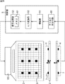
図1の表示装置1は、ELパネル2、複数の受光センサ3からなるセンサ群4、および制御部5を含むように構成されている。ELパネル2は、有機ELデバイスを自発光素子として用いたパネルとして構成されている。受光センサ3は、ELパネル2の発光輝度を測定するセンサとして構成されている。制御部5は、複数の受光センサ3から得たELパネル2の発光輝度に基づいてELパネル2の表示を制御する。
The
[ELパネルの構成]
図2は、ELパネル2の構成例を示すブロック図である。
[Configuration of EL panel]
FIG. 2 is a block diagram illustrating a configuration example of the
ELパネル2は、画素アレイ部102、水平セレクタ(HSEL)103、ライトスキャナ(WSCN)104、および電源スキャナ(DSCN)105を含むように構成されている。画素アレイ部102は、N×M個(N,Mは相互に独立した1以上の整数値)の画素(画素回路)101−(1,1)乃至101−(N,M)が行列状に配置されて構成されている。水平セレクタ(HSEL)103、ライトスキャナ(WSCN)104、および電源スキャナ(DSCN)105は、画素アレイ部102を駆動する駆動部として動作する。
The
また、ELパネル2は、M本の走査線WSL10−1乃至10−M、M本の電源線DSL10−1乃至10−M、およびN本の映像信号線DTL10−1乃至10−Nも有する。
The
なお、以下において、走査線WSL10−1乃至10−Mそれぞれを特に区別する必要がない場合、単に、走査線WSL10と称する。また、映像信号線DTL10−1乃至10−Nそれぞれを特に区別する必要がない場合、単に、映像信号線DTL10と称する。画素101−(1,1)乃至101−(N,M)および電源線DSL10−1乃至10−Mについても同様に、画素101および電源線DSL10と称する。
In the following description, the scanning lines WSL10-1 to 10-M are simply referred to as scanning lines WSL10 when it is not necessary to distinguish them. Further, when it is not necessary to distinguish each of the video signal lines DTL10-1 to 10-N, they are simply referred to as a video signal line DTL10. Similarly, the pixels 101- (1,1) to 101- (N, M) and the power supply lines DSL10-1 to 10-M are also referred to as the
画素101−(1,1)乃至101−(N,M)のうちの第1行目の画素101−(1,1)乃至101−(N,1)は、走査線WSL10−1でライトスキャナ104と、電源線DSL10−1で電源スキャナ105とそれぞれ接続されている。また、画素101−(1,1)乃至101−(N,M)のうちの第M行目の画素101−(1,M)乃至101−(N,M)は、走査線WSL10−Mでライトスキャナ104と、電源線DSL10−Mで電源スキャナ105とそれぞれ接続されている。画素101−(1,1)乃至101−(N,M)の行方向に並ぶその他の画素101についても同様である。
Among the pixels 101- (1,1) to 101- (N, M), the pixels 101- (1,1) to 101- (N, 1) in the first row are scanned by the scanning line WSL10-1. 104 and the
また、画素101−(1,1)乃至101−(N,M)のうちの第1列目の画素101−(1,1)乃至101−(1,M)は、映像信号線DTL10−1で水平セレクタ103と接続されている。画素101−(1,1)乃至101−(N,M)のうちの第N列目の画素101−(N,1)乃至101−(N,M)は、映像信号線DTL10−Nで水平セレクタ103と接続されている。画素101−(1,1)乃至101−(N,M)の列方向に並ぶその他の画素101についても同様である。
Among the pixels 101- (1,1) to 101- (N, M), the pixels 101- (1,1) to 101- (1, M) in the first column are video signal lines DTL10-1. Is connected to the
ライトスキャナ104は、走査線WSL10−1乃至10−Mに水平周期(1H)で順次制御信号を供給して画素101を行単位で線順次走査する。電源スキャナ105は、線順次走査に合わせて電源線DSL10−1乃至10−Mに第1電位(後述するVcc)または第2電位(後述するVss)の電源電圧を供給する。水平セレクタ103は、線順次走査に合わせて各水平期間内(1H)で映像信号に対応する信号電位Vsigと基準電位Vofsとを切換えて列状の映像信号線DTL10−1乃至10−Mに供給する。
The
[画素101の配列構成]
図3は、ELパネル2の各画素101が発光する色の配列を示している。
[Array Configuration of Pixels 101]
FIG. 3 shows an arrangement of colors emitted by the
画素アレイ部102の各画素101は、赤(R)、緑(G)、または青(B)のいずれかの色を発光するいわゆる副画素(サブピクセル)に相当し、行方向(図面左右方向)に並ぶ赤、緑、および青の3つの画素101で表示単位としての1画素が構成される。
Each
なお、図3では、ライトスキャナ104が画素アレイ部102の左側に配置されるとともに、走査線WSL10および電源線DSL10が画素101の下側から接続されている点が図2と異なる。水平セレクタ103、ライトスキャナ104、電源スキャナ105、および、各画素101と接続される配線は、必要に応じて適切な位置に配置することができる。
3 is different from FIG. 2 in that the
[画素101の詳細回路構成]
図4は、ELパネル2に含まれるN×M個の画素101のうちの1つの画素101を拡大することにより、画素101の詳細な回路構成を示したブロック図である。
[Detailed Circuit Configuration of Pixel 101]
FIG. 4 is a block diagram showing a detailed circuit configuration of the
なお、図4において画素101と接続されている走査線WSL10、映像信号線DTL10、および電源線DSL10のそれぞれは、図2に対応させると次のようになる。即ち、図2における画素101−(n,m)(n=1,2,・・・,N,m=1,2,・・・,M)に対する、走査線WSL10−(n,m)、映像信号線DTL10−(n,m)、および電源線DSL10−(n,m)のそれぞれが対応する。
In FIG. 4, each of the scanning line WSL10, the video signal line DTL10, and the power supply line DSL10 connected to the
図4の画素101は、サンプリング用トランジスタ31、駆動用トランジスタ32、蓄積容量33、および発光素子34を有する。サンプリング用トランジスタ31のゲートは走査線WSL10と接続され、サンプリング用トランジスタ31のドレインは映像信号線DTL10と接続されるとともに、ソースが駆動用トランジスタ32のゲートgと接続されている。
The
駆動用トランジスタ32のソース及びドレインの一方は発光素子34のアノードに接続され、他方が電源線DSL10に接続される。蓄積容量33は、駆動用トランジスタ32のゲートgと発光素子34のアノードに接続されている。また、発光素子34のカソードは所定の電位Vcatに設定されている配線35に接続されている。この電位VcatはGNDレベルであり、従って、配線35は接地配線である。
One of the source and the drain of the driving
サンプリング用トランジスタ31および駆動用トランジスタ32は、いずれもNチャネル型トランジスタである。よって、サンプリング用トランジスタ31および駆動用トランジスタ32は、低温ポリシリコンよりも安価に作成できるアモルファスシリコンで作成することができる。これにより、画素回路の製造コストをより安価にすることができる。勿論、サンプリング用トランジスタ31および駆動用トランジスタ32は、低温ポリシリコンや単結晶シリコンで作成しても構わない。
The
発光素子34は、有機EL素子で構成される。有機EL素子はダイオード特性を有する電流発光素子である。よって、発光素子34は、供給される電流値Idsに応じた階調の発光を行う。
The
以上のように構成される画素101において、サンプリング用トランジスタ31が、走査線WSL10からの制御信号に応じてオン(導通)し、映像信号線DTL10を介して階調に応じた信号電位Vsigの映像信号をサンプリングする。蓄積容量33は、映像信号線DTL10を介して水平セレクタ103から供給された電荷を蓄積して保持する。駆動用トランジスタ32は、第1電位Vccにある電源線DSL10から電流の供給を受け、蓄積容量33に保持された信号電位Vsigに応じて駆動電流Idsを発光素子34に流す(供給する)。発光素子34に所定の駆動電流Idsが流れることにより、画素101が発光する。
In the
画素101は、閾値補正機能を有する。閾値補正機能とは、駆動用トランジスタ32の閾値電圧Vthに相当する電圧を蓄積容量33に保持させる機能である。閾値補正機能を発揮させることで、ELパネル2の画素毎のばらつきの原因となる駆動用トランジスタ32の閾値電圧Vthの影響をキャンセルすることができる。
The
また、画素101は、上述した閾値補正機能に加え、移動度補正機能も有する。移動度補正機能とは、蓄積容量33に信号電位Vsigを保持する際、駆動用トランジスタ32の移動度μに対する補正を信号電位Vsigに加える機能である。
Further, the
さらに、画素101は、ブートストラップ機能も備えている。ブートストラップ機能とは、駆動用トランジスタ32のソース電位Vsの変動にゲート電位Vgを連動させる機能である。ブートストラップ機能の発揮により、駆動用トランジスタ32のゲートとソース間の電圧Vgsを一定に維持することが出来る。
Furthermore, the
[画素101の動作説明]
図5は、画素101の動作を説明するタイミングチャートである。
[Description of Operation of Pixel 101]
FIG. 5 is a timing chart for explaining the operation of the
図5は、同一の時間軸(図面横方向)に対する走査線WSL10、電源線DSL10、および映像信号線DTL10の電位変化と、それに対応する駆動用トランジスタ32のゲート電位Vg及びソース電位Vsの変化を示している。
FIG. 5 shows changes in potentials of the scanning line WSL10, the power supply line DSL10, and the video signal line DTL10 with respect to the same time axis (horizontal direction in the drawing), and changes in the gate potential Vg and source potential Vs of the driving
図5において、時刻t1までの期間は、前の水平期間(1H)の発光がなされている発光期間T1である。 In FIG. 5, the period up to time t 1 is the light emission period T 1 during which light is emitted in the previous horizontal period (1H).
発光期間T1が終了した時刻t1から時刻t4までは、駆動用トランジスタ32のゲート電位Vg及びソース電位Vsを初期化することで閾値電圧補正動作の準備を行う閾値補正準備期間T2である。
From time t 1 to time t 4 when the light emission period T 1 ends, a threshold correction preparation period T 2 in which the gate potential Vg and the source potential Vs of the driving
閾値補正準備期間T2では、時刻t1において、電源スキャナ105が、電源線DSL10の電位を高電位である第1電位Vccから低電位である第2電位Vssに切換える。そして、時刻t2において、水平セレクタ103が、映像信号線DTL10の電位を信号電位Vsigから基準電位Vofsに切換える。次に、時刻t3において、ライトスキャナ104が、走査線WSL10の電位を高電位に切換え、サンプリング用トランジスタ31をオンさせる。これにより、駆動用トランジスタ32のゲート電位Vgが基準電位Vofsにリセットされ、且つ、ソース電位Vsが映像信号線DTL10の第2電位Vssにリセットされる。
In the threshold value correction preparation period T 2, at time t 1, the
時刻t4から時刻t5までは、閾値補正動作を行う閾値補正期間T3である。閾値補正期間T3では、時刻t4において、電源スキャナ105により、電源線DSL10の電位が高電位Vccに切換えられ、閾値電圧Vthに相当する電圧が、駆動用トランジスタ32のゲートとソースとの間に接続された蓄積容量33に書き込まれる。
From time t 4 to time t 5 is a threshold correction period T 3 in which the threshold correction operation is performed. In the threshold correction period T 3 , at time t 4 , the
時刻t5から時刻t7までの書き込み+移動度補正準備期間T4では、走査線WSL10の電位が高電位から低電位に一旦切換えられる。また、時刻t7の前の時刻t6において、水平セレクタ103が、映像信号線DTL10の電位を基準電位Vofsから階調に応じた信号電位Vsigに切換える。
In the writing + mobility correction preparation period T 4 from time t 5 to time t 7 , the potential of the
そして、時刻t7から時刻t8までの書き込み+移動度補正期間T5において、映像信号の書き込みと移動度補正動作が行われる。即ち、時刻t7から時刻t8までの間、走査線WSL10の電位が高電位に設定され、これにより、映像信号に対応する信号電位Vsigが閾値電圧Vthに足し込まれる形で蓄積容量33に書き込まれる。また、移動度補正用の電圧ΔVμが蓄積容量33に保持された電圧から差し引かれる。
Then, in the writing + mobility correction period T 5 from time t 7 to time t 8 , video signal writing and mobility correction operation are performed. That is, between the time t 7 to the time t 8, the potential of the scanning line WSL10 is set to a high potential, Thus, the
書き込み+移動度補正期間T5終了後の時刻t8において、走査線WSL10の電位が低電位に設定され、それ以降、発光期間T6として、信号電圧Vsigに応じた発光輝度で発光素子34が発光する。信号電圧Vsigは、閾値電圧Vthに相当する電圧と移動度補正用の電圧ΔVμとによって調整されているため、発光素子34の発光輝度は駆動用トランジスタ32の閾値電圧Vthや移動度μのばらつきの影響を受けることがない。
Write + in the mobility correction period T 5 after the end of the time t 8, the potential of the scanning line WSL10 is set to a low potential, thereafter, as a light-emitting period T 6, the
なお、発光期間T6の最初でブートストラップ動作が行われ、駆動用トランジスタ32のゲート‐ソース間電圧Vgs=Vsig+Vth−ΔVμを一定に維持したまま、駆動用トランジスタ32のゲート電位Vg及びソース電位Vsが上昇する。
Note that a bootstrap operation is performed at the beginning of the light emission period T 6 , and the gate potential Vg and the source potential of the driving
また、時刻t8から所定時間経過後の時刻t9において、映像信号線DTL10の電位が、信号電位Vsigから基準電位Vofsに落とされる。図5において、時刻t2から時刻t9までの期間は水平期間(1H)に相当する。 At time t 9 after a predetermined time from the time t 8, the potential of the video signal line DTL10 is dropped from the signal potential Vsig to the reference potential Vofs. In FIG. 5, the period from time t 2 to time t 9 corresponds to the horizontal period (1H).
以上のようにして、ELパネル2の各画素101では、駆動用トランジスタ32の閾値電圧Vthや移動度μのばらつきの影響を受けることがなく、発光素子34を発光させることができる。
As described above, each
[画素101の動作の別の例説明]
図6は、画素101の動作の別の例を説明するタイミングチャートである。
[Description of another example of the operation of the pixel 101]
FIG. 6 is a timing chart for explaining another example of the operation of the
上述した図5の例では、閾値補正動作は1H期間に1回行われていた。ただし、1H期間が短く、1H期間内で閾値補正動作を行うことが難しい場合がある。そのような場合には、複数の1H期間にわたって複数回の閾値補正動作を行わせることができる。行うこともできる。 In the example of FIG. 5 described above, the threshold correction operation is performed once in the 1H period. However, the 1H period is short, and it may be difficult to perform the threshold correction operation within the 1H period. In such a case, the threshold correction operation can be performed a plurality of times over a plurality of 1H periods. It can also be done.
図6の例では、閾値補正動作は、連続する3H期間で行われる。即ち、図6の例では、閾値補正期間T3が3回に分割されている。なお、その他の画素101の動作は、図5の例の動作と同様である。よって、これらの動作の説明については省略する。
In the example of FIG. 6, the threshold correction operation is performed in a continuous 3H period. That is, in the example of FIG. 6, the threshold correction period T 3 is divided into three times. The other operations of the
[焼き付き補正制御の説明] [Explanation of burn-in correction control]
ところで、有機ELデバイスは、発光量および発光時間に比例して発光輝度が低下する特性を有している。そのため、所定の時間が経過すると、同一の駆動条件下でも、それまでの発光量および発光時間に応じて各画素101の輝度効率の低下の度合いが異なってくる。このため、各画素101の輝度効率低下のばらつきにより、輝度効率の低下度合が他と比較して著しい画素101が生じる。その結果、かかる画素101において、あたかも焼き付きが生じているような現象(以下、焼き付き現象と称する)がユーザに視認される。そこで、表示装置1は、輝度効率低下がまちまちである各画素101に対して、各輝度効率を統一にする補正(以下、焼き付き補正と称する)を行っている。
By the way, the organic EL device has a characteristic that the light emission luminance decreases in proportion to the light emission amount and the light emission time. For this reason, when a predetermined time elapses, the degree of decrease in luminance efficiency of each
[焼き付き補正制御を実行するために必要な表示装置1の機能的構成例]
図7は、焼き付き補正制御を実行するために必要な表示装置1の機能的構成例を示す機能ブロック図を示している。
[Example of Functional Configuration of
FIG. 7 is a functional block diagram illustrating a functional configuration example of the
受光センサ3は、ELパネル2の表示面またはそれと対向する面(以下、前者の面を表面と、後者の面を裏面と、それぞれ称する)のうち、各画素101の発光の妨げとならない位置に配置される。また、ELパネル2が複数の領域に区分され、その領域毎に1つの受光センサ3が配置される。即ち、1つの領域につき1個の割合で均等に配置された複数の受光センサ3により、センサ群4が構成されている。例えば、図7の例では、センサ群4は9個の受光センサ3により構成されている。勿論ELパネル2に配置される受光センサ3の個数は、図7の例に限定されるものではない。
The
各受光センサ3のそれぞれは、自分が担当する領域内の各画素101からの光を受光し、それらの受光量に応じたアナログの受光信号(電圧信号)を生成し、制御部5に供給する。なお、受光センサ3がELパネル2の裏面に配置されている場合、各画素101から発光された光は、ELパネル2の前面のガラス基板等に反射して、受光センサ3に入射する。本発明の実施の形態においては、受光センサ3がELパネル2の裏面に配置されているとする。
Each of the
図7の例では、制御部5は、増幅部51、A/D変換部52、および信号処理部53を含むように構成されている。
In the example of FIG. 7, the
増幅部51は、各受光センサ3から供給されるアナログの受光信号を増幅してA/D変換部52に供給する。A/D変換部52は、増幅部51から供給される増幅後のアナログの受光信号をデジタルデータに変換し、信号処理部53に供給する。
The
信号処理部53のメモリ61には、画素アレイ部102の各画素101について、輝度データの初期値(出荷状態時の輝度データ)が初期データとして記憶されている。信号処理部53は、処理の対象として注目すべき画素101(以下、注目画素Pと称する)についてのデジタルデータがA/D変換部52から供給されてきたとき、そのデジタルデータに基づいて、所定期間経過後(経時劣化後)の注目画素Pの輝度データを認識する。信号処理部53は、注目画素Pについて、所定期間経過後の輝度値の初期データ(初期輝度値)に対する輝度低下量を算出する。そして、信号処理部53は、注目画素Pについて、輝度低下を補正する補正データを、その輝度低下量に基づいて演算する。このような補正データは、画素アレイ部102の各画素101が注目画素Pに順次設定されることで、各画素101毎に算出され、メモリ61に記憶される。
The
なお、信号処理部53のうち、上述の補正データを演算する部分は、例えば、FPGA(Field Programmable Gate Alley)、ASIC(Application Specific Integrated Circuit)などの信号処理ICで構成することができる。 In addition, the part which calculates the above-mentioned correction data among the signal processing parts 53 can be comprised by signal processing IC, such as FPGA (Field Programmable Gate Alley) and ASIC (Application Specific Integrated Circuit).
以上説明したように、メモリ61には、所定期間経過時点の各画素101の補正データが記憶される。また、メモリ61には、各画素101についての初期データも記憶される。その他、メモリ61には、後述する各種処理を実現する上で必要な各種情報も記憶される。
As described above, the
信号処理部53はまた、水平セレクタ103を制御して、各画素101毎に、表示装置1に入力された映像信号に対応する信号電位Vsigを供給させる。このとき、信号処理部53は、各画素101の補正データをメモリ61からそれぞれ読み出して、経時劣化による輝度低下を補正した信号電位Vsigを各画素101毎に決定する。
The signal processing unit 53 also controls the
[従来の焼き付き補正制御] [Conventional burn-in correction control]
ここで、[発明が解決しようとする課題]の欄で説明した従来の焼き付き補正制御の問題点を説明する。 Here, the problem of the conventional burn-in correction control described in the section “Problems to be solved by the invention” will be described.
上述の如く、焼き付き補正制御では、注目画素Pの輝度データが用いられる。注目画素の輝度データは、受光センサ3の受光信号が増幅され、増幅後のアナログの信号に対してA/D変換が施された結果得られるデジタルデータに基づいて生成される。
As described above, in the burn-in correction control, the luminance data of the target pixel P is used. The luminance data of the pixel of interest is generated based on digital data obtained as a result of amplifying the light reception signal of the
しかしながら、図7に示されるように、1つの画素101に対して1つの受光センサ3が用いられるのではなく、複数の画素101から構成される領域に対して1つの受光センサ3が用いられている。よって、領域を構成する各画素101のそれぞれと、受光センサ3との間の距離はまちまちになる。このような場合の受光センサ3の受光信号の出力電圧は図8に示されるようになる。
However, as shown in FIG. 7, one
図8は、20×20の画素101から構成される領域の中心に受光センサ3が配置されている場合における、受光センサ3の出力電圧の関係の例を示す図である。前提として、20×20の各画素101の発光輝度自体は同一に保たれている。図8のAにおいて、横軸は、受光センサ3からの水平方向の距離(単位は画素数)を示しており、縦軸は、受光センサ3の出力電圧(mV)を示している。図8のBにおいて、横軸は、受光センサ3からの垂直方向の距離(単位は画素数)を示しており、縦軸は、受光センサ3の出力電圧(mV)を示している。
FIG. 8 is a diagram illustrating an example of the relationship between the output voltages of the
図8に示されるように、領域を構成する各画素101の発光輝度自体は同一に保っても、受光センサ3の受光信号の出力電圧は、各画素101と受光センサ3との間の距離が長くなるほど小さくなっていく。このような特性を一般化すると、図9に示されるような特性を受光センサ3は有していることになる。
As shown in FIG. 8, the output voltage of the light reception signal of the
図9は、受光センサ3の出力電圧の、画素101との間の距離の依存性の関係を示す図である。図9において、縦軸は、受光センサ3の出力電圧を示している。横軸は、受光センサ3からの所定方向の距離(単位は画素数)を示している。
FIG. 9 is a diagram showing the relationship of the dependence of the output voltage of the
図10は、受光センサ3の受光時間と受光電流の関係を示す図である。図10において、縦軸は、受光センサ3の受光時間(s)を示している。横軸は、受光センサ3の受光電流(A)を示している。
FIG. 10 is a diagram showing the relationship between the light receiving time of the
図9に示されるように、受光センサ3との距離が画素数にして0だけ離れている画素101(以下、距離0の画素101と称する)が注目画素Pとして設定された場合、受光センサ3の出力電圧はVoとなる。これに対して、注目画素Pとして、受光センサ3との距離が画素数にしてα(αは1以上の整数値)だけ離れている画素101(以下、距離αの画素101と称する)が設定された場合、注目画素Pの発光輝度が距離0の画素101と同一であったとしても、受光センサ3の出力電圧はVoよりも遥かに低いVαとなる。受光センサ3の出力電圧が低くなることとは、受光センサ3の受光電流が小さくなることを意味している。そして、図10によれば、受光センサ3には、受光電流が小さくなる程その受光時間が長くなっていくという特性、即ち、出力電圧を出力するまでの応答時間が長くなるという特性が存在する。
As shown in FIG. 9, when a
しかしながら、かかる特性を従来考慮していなかったことが、[発明が解決しようとする課題]で生ずる問題点、即ち、補正システム全体の処理時間が長時間となってしまうという問題点の発生要因である。以下、図11を参照して、このことについてさらに詳しく説明する。 However, the fact that such characteristics have not been considered in the past is the cause of the problem that arises in [Problems to be solved by the invention], that is, the processing time of the entire correction system becomes long. is there. Hereinafter, this will be described in more detail with reference to FIG.
図11は、従来の焼き付き補正制御を説明する図である。 FIG. 11 is a diagram for explaining conventional burn-in correction control.
図11のA乃至Gには、5×5の画素101から構成される領域が示されている。この領域の中心には、受光センサ3が配置されている。
In FIGS. 11A to 11G, an area composed of 5 × 5
図11のAは、焼き付き補正制御における注目画素Pの設定順序を示している。処理対象行がi行(図11の例では、iは1乃至5のうちの何れかの整数値)である場合、i行目に配置されている5つの画素101のそれぞれが、左端(1列目)の画素101から右端(5列目)の画素101に向かう順番で順次注目画素Pとして設定されていく。そして、i行の右端(5列目)の画素101が注目画素Pに設定されると、処理対象行は、次のi+1行に遷移し、i行と同様の順序で注目画素Pが順次設定されていく。
FIG. 11A shows the setting order of the target pixel P in the burn-in correction control. When the processing target row is i rows (in the example of FIG. 11, i is any integer value from 1 to 5), each of the five
この場合、従来の焼き付き補正制御においては、信号処理部53は、注目画素Pのみを予め決められた所定の階調で発光させる。即ち、信号処理部53は、それ以外の24個の画素101を消光させる。
In this case, in the conventional burn-in correction control, the signal processing unit 53 causes only the target pixel P to emit light with a predetermined gradation. That is, the signal processing unit 53 extinguishes the other 24
即ち、図11のBに示されるように、最初に、1行目が処理対象行となり、1列目の画素101が注目画素Pとなる。よって、1行1列目の注目画素Pのみが、予め決められた所定の階調で発光する。すると、受光センサ3は、注目画素Pの受光輝度に応じた受光信号(電圧信号)を制御部5に出力する。制御部5は、注目画素Pの受光信号に基づいて、注目画素Pの補正データを算出し、メモリ61に記憶させる。
That is, as shown in FIG. 11B, first, the first row becomes the processing target row, and the
次に、図11のCに示されるように、信号処理部53は、これまで注目画素Pとされていた1行1列の画素101の右隣の画素101、即ち、1行2列目の画素101を注目画素Pに設定する。よって、1行2列目の注目画素Pのみが、予め決められた所定の階調で発光する。すると、受光センサ3は、注目画素Pの受光輝度に応じた受光信号(電圧信号)を制御部5に出力する。制御部5は、注目画素Pの受光信号に基づいて、注目画素Pの補正データを算出し、メモリ61に記憶させる。
Next, as illustrated in C of FIG. 11, the signal processing unit 53 performs the
以下、図11のD乃至Gに示されるように、上述の順番で注目画素Pが順次設定され、注目画素Pの受光信号が受光センサ3から出力される。その結果、注目画素Pの受光信号に基づいて、注目画素Pの補正データが算出されてメモリ61に記憶される。
Hereinafter, as illustrated in D to G of FIG. 11, the target pixel P is sequentially set in the above-described order, and the light receiving signal of the target pixel P is output from the
ここで、図11のBの注目画素Pと、図11のFの注目画素Pとに着目する。この場合、図11のBの注目画素Pと受光センサ3との間の距離は、図11のFの注目画素Pと受光センサ3との間の距離よりも遠い。よって、受光センサ3が注目画素Pからの光を受光してその受光信号を出力するまでの応答時間は、注目画素Pが図11のBの場合の方が、図11のFの場合よりも長くなる。その結果、図11のBの注目画素Pの補正データが生成されてメモリ61に記憶されるまでの一連の処理時間は、図11のFの注目画素Pについての一連の処理時間よりも長くなってしまう。
Here, attention is focused on the target pixel P in FIG. 11B and the target pixel P in FIG. 11F. In this case, the distance between the target pixel P in FIG. 11B and the
このように、注目画素Pとして設定された画素101と受光センサ3との間の距離が遠方になればなる程、その補正データが生成されてメモリ61に記憶されるまでの一連の処理時間は長くなる。即ち、図11のBのように受光センサ3から遠距離に位置する画素101が存在する分だけ、焼き付き補正システム全体の応答時間が長くなってしまう。このようにして、[発明が解決しようとする課題]の欄で説明した従来の焼き付き補正制御の問題点が発生してしまう。
Thus, as the distance between the
そこで、本問題点を解決すべく、即ち、焼き付き補正システムの処理時間の短縮を図るべく、本発明人は、次のような焼き付き補正制御手法を発明した。即ち、受光センサ3との距離が遠方である画素101に対する受光センサ3の受光強度を高めて焼き付き補正を行う、という焼き付き補正制御手法が本発明人により発明された。以下、かかる手法を、本発明の焼き付き補正制御手法と称する。
In order to solve this problem, that is, in order to shorten the processing time of the burn-in correction system, the present inventors have invented the following burn-in correction control method. That is, the inventor has invented a burn-in correction control method in which burn-in correction is performed by increasing the light-receiving intensity of the light-receiving
[本発明の焼き付き補正制御手法の第1の例]
図12は、本発明の焼き付き補正制御手法の第1の例を説明する図である。
[First example of burn-in correction control method of the present invention]
FIG. 12 is a diagram for explaining a first example of the burn-in correction control method of the present invention.
図12のA乃至Hには、5×5の画素101から構成される領域が示されている。この領域の中心には、受光センサ3が配置されている。図12において、画素101を示すブロック内の模様のうち、網かけの模様(薄い模様)は、一定の階調で画素101が発光していることを示している。一方、右斜線の模様(濃い模様)は、画素101が消光していることを示している。
In FIGS. 12A to 12H, an area composed of 5 × 5
第1の例では、信号処理部53は、領域を構成する各画素101の全てを発光させたうえで、焼き付き補正制御を行う。このようにすることで、受光センサ3の受光強度上げることができ、受光センサ3の受光時間を短縮すること、即ち、受光センサ3の応答速度を上げることができる。
In the first example, the signal processing unit 53 performs burn-in correction control after causing all the
図12のAは、第1の例における注目画素Pの設定順序を示している。注目画素Pの設定順序自体は、図11のAの注目画素Pの設定順序と同様とされている。 FIG. 12A shows the setting order of the target pixel P in the first example. The setting order of the target pixel P itself is the same as the setting order of the target pixel P in A of FIG.
初期状態として、図12のBに示されるように、信号処理部53は、領域を構成する各画素101を所定の階調で一律に発光させる。
As an initial state, as shown in FIG. 12B, the signal processing unit 53 uniformly emits the
その後、図12のC乃至Hに示されるように、信号処理部53は、領域を構成する25個(=5×5個)の画素101を1つずつ、上述の順番で注目画素Pに順次設定していく。そして、信号処理部53は、注目画素Pとなった画素101のみを順次消光させていく。即ち、注目画素P以外の24個の画素101は、所定の階調での発光を維持する。
Thereafter, as shown in FIGS. 12C to 12H, the signal processing unit 53 sequentially adds the 25 (= 5 × 5)
このように、図12のBの初期状態において、領域を構成する各画素101は全て所定の階調で一律に発光する。その結果、受光センサ3には、領域を構成する各画素101から発光されたそれぞれの光が到達することになる。よって、初期状態の受光センサ3の出力電圧(受光信号の電圧)は、これらの25個(=5×5個)の画素101から到達した全ての光の積算量(以下、全画素光積算量と称する)を示すことになる。ここで、図12のC乃至Hに示されるように、注目画素Pのみを消光させると、受光センサ3の出力電圧(受光信号の電圧)は、全画素光積算値に対して、注目画素Pが消光した分(=注目画素Pの発光輝度分)だけ低くなる。よって、初期状態の受光センサ3の受光信号と、注目画素Pだけ消光させた状態(以下、注目画素消光状態と称する)の受光センサ3の受光信号との差分を取ると、注目画素Pの発光輝度が得られることになる。
Thus, in the initial state of B in FIG. 12, all the
そこで、第1の例では、初期状態(図12のBの状態)の受光センサ3の受光信号が増幅され、A/D変換された結果得られるデジタルデータが、オフセットデータとしてメモリ61に予め記憶される。この場合、オフセットデータの値は、アナログ信号に換算すると(A/D変換前の状態では)、例えば図13に示される値となる。
Therefore, in the first example, the light reception signal of the
図13は、本発明の焼き付き補正制御手法の第1の例のうち、注目画素の輝度値の算出手法を説明する図である。図13において、縦軸は、受光センサ3の受光信号の増幅後の電圧を示している。横軸は、受光センサ3からの所定方向の距離(単位は画素数)を示している。
FIG. 13 is a diagram for explaining a method for calculating the luminance value of the target pixel in the first example of the burn-in correction control method according to the present invention. In FIG. 13, the vertical axis indicates the voltage after amplification of the light reception signal of the
ここで、注目画素消光状態での受光センサ3の受光信号が増幅され、A/D変換された結果得られるデジタルデータを、受光データと称することにする。この場合、受光データのアナログ信号の換算値(A/D変換前の状態の値)は、図13に示されるように、オフセットデータの値に対して、注目画素Pが消光した分(=注目画素Pの発光輝度分)だけ低くなる。そこで、信号処理部53は、オフセットデータの値から、注目画素Pの受光データの値を減算することで、注目画素の輝度値を算出できるようになる。
Here, the digital data obtained as a result of the amplification of the light reception signal of the
なお、図13において、受光センサ3に近づく程受光データの値が低くなっている理由は、図9を用いて説明したように、画素101の発光輝度自体は同一であっても、受光センサ3に近いほど、受光センサ3が感知する受光量が多くなるからである。即ち、全画素光積算値の中で、注目画素Pの発光に基づく受光量が占める割合は、注目画素Pが受光センサ3に近づくほど高くなるからである。
In FIG. 13, the reason why the light reception data value becomes lower as the
ここで注目すべき点は、受光センサ3から遠方の画素101が注目画素Pに設定された場合であっても、受光データの値は一定以上の値を保っている点、即ち、オフセットデータの値に近い値を保っている点である。即ち、注目画素消光状態の受光センサ3の出力電圧(受光信号の電圧)は、受光センサ3と注目画素Pとの間の距離によらず、一定以上の値を確保している点である。このことは、受光センサ3は、注目画素Pとの間の距離によらず、一定以上の応答速度で受光信号を常に出力できる、ことを意味する。よって、焼き付き補正システム全体の処理時間として総合的に従来と比較すると、その処理時間の短縮を図ることができるようになるのである。即ち、上述した問題を解決できるようになるのである。
The point to be noted here is that even when the
なお、上述の如く、注目画素Pの輝度値は、オフセットデータの値との差分さえ測定できれば算出可能である。よって、注目画素Pは、消光させるのではなく、周囲の画素101の発光輝度の階調よりも低い階調で発光させるようにしてもよい。
As described above, the luminance value of the target pixel P can be calculated as long as the difference from the offset data value can be measured. Therefore, the target pixel P may not be extinguished, but may be made to emit light at a gradation lower than the gradation of the light emission luminance of the surrounding
[本発明の焼き付き補正制御手法の第1の例が適用された初期データ取得処理] [Initial data acquisition process to which the first example of the burn-in correction control method of the present invention is applied]
図14は、表示装置1が実行する処理のうち、本発明の焼き付き補正制御手法の第1の例を実現するための初期データを取得するまでの一連の処理(以下、初期データ取得処理)の一例を説明するフローチャートである。
FIG. 14 shows a series of processes (hereinafter referred to as initial data acquisition process) up to acquiring initial data for realizing the first example of the burn-in correction control method of the present invention, among the processes executed by the
図14の例の初期データ取得処理は、例えば、ELパネル2が区分された各領域毎に並行して実行される。即ち、図14の初期データ取得処理は、各受光センサ3毎に並行して実行される。
The initial data acquisition process in the example of FIG. 14 is executed in parallel for each area into which the
ステップS1において、信号処理部53は、図13を用いて説明したオフセットデータを生成し、メモリ61に記憶させる。なお、以下、オフセットデータを生成し、メモリ61に記憶させるまでの一連の処理を、オフセット値取得処理と称する。ここで、オフセット値取得処理の詳細例について、図15を参照して説明する。
In step S <b> 1, the signal processing unit 53 generates the offset data described with reference to FIG. 13 and stores it in the
[オフセット値取得処理] [Offset value acquisition processing]
図15は、本発明が適用されるオフセット値取得処理の一例を説明するフローチャートである。 FIG. 15 is a flowchart illustrating an example of an offset value acquisition process to which the present invention is applied.
ステップS21において、信号処理部53は、領域を構成する各画素101を所定の階調で発光させる。
In step S21, the signal processing unit 53 causes each
ステップS22において、受光センサ3は、領域を構成する各画素101全体の受光輝度に応じたアナログの受光信号(電圧信号)を制御部5の増幅部51に出力する。
In step S <b> 22, the
ステップS23において、増幅部51は、受光センサ3の受光信号を所定の増幅率で増幅し、A/D変換部52に供給する。
In step S <b> 23, the
ステップS24において、A/D変換部52は、増幅後のアナログの受光信号を、デジタルの信号であるオフセットデータに変換し、信号処理部53に供給する。 In step S <b> 24, the A / D conversion unit 52 converts the amplified analog light reception signal into offset data that is a digital signal and supplies the offset data to the signal processing unit 53.
ステップS25において、信号処理部53は、オフセットデータをメモリ61に記憶させる。
In step S <b> 25, the signal processing unit 53 stores the offset data in the
これにより、オフセット値取得処理は終了する。いまの場合、図14のステップS1の処理が終了し、処理はステップS2に進む。 Thereby, the offset value acquisition process ends. In this case, the process of step S1 in FIG. 14 ends, and the process proceeds to step S2.
ステップS2において、信号処理部53は、領域を構成する各画素101のうち輝度データが取得されていない画素101を注目画素Pに設定する。なお、注目画素Pの設定順序は、図12のAを用いて説明した通りである。
In step S <b> 2, the signal processing unit 53 sets the
ステップS3において、信号処理部53は、注目画素Pを、消光させる。即ち、図12のC乃至Hに示されるように、領域を構成する各画素101のうち、注目画素Pのみが消光し、それ以外の画素101は発光を維持する。
In step S3, the signal processing unit 53 extinguishes the target pixel P. That is, as shown in FIGS. 12C to 12H, only the pixel of interest P is extinguished among the
ステップS4において、受光センサ3は、領域を構成する各画素101のうちの注目画素Pを除く画素101全体の受光輝度に応じたアナログの受光信号(電圧信号)を制御部5の増幅部51に出力する。
In step S <b> 4, the
ステップS5において、増幅部51は、受光センサ3の受光信号を所定の増幅率で増幅し、A/D変換部52に供給する。
In step S <b> 5, the
ステップS6において、A/D変換部52は、増幅後のアナログの受光信号を、デジタルの信号である受光データに変換し、信号処理部53に供給する。 In step S <b> 6, the A / D conversion unit 52 converts the amplified analog light reception signal into light reception data that is a digital signal, and supplies the light reception data to the signal processing unit 53.
ステップS7において、信号処理部53は、オフセットデータの値と受光データの値との差分を取ることにより、注目画素の輝度値を算出する(図13参照)。 In step S7, the signal processing unit 53 calculates the luminance value of the target pixel by taking the difference between the value of the offset data and the value of the received light data (see FIG. 13).
ステップS8において、信号処理部53は、注目画素の輝度値を示す輝度データを初期データとしてメモリ61に記憶させる。
In step S <b> 8, the signal processing unit 53 stores luminance data indicating the luminance value of the target pixel in the
ステップS9において、信号処理部53は、領域内のすべての画素101について輝度データを取得したかを判定する。ステップS9において、領域内のすべての画素101についてまだ輝度データを取得していないと判定された場合、処理はステップS2に戻され、ステップS2乃至S9の処理のループ処理が繰り返される。即ち、領域を構成する各画素101のそれぞれが順次注目画素Pに設定され、かかるループ処理が繰り返し実行されることで、領域を構成する全画素101の初期データが取得されメモリ61に記憶される。
In step S9, the signal processing unit 53 determines whether luminance data has been acquired for all the
これにより、ステップS9において、領域内のすべての画素101について輝度データを取得したと判定されて、初期データ取得処理は終了する。
Thereby, in step S9, it is determined that the luminance data has been acquired for all the
[本発明の焼き付き補正制御手法の第1の例が適用された補正データ取得処理] [Correction data acquisition processing to which the first example of the burn-in correction control method of the present invention is applied]
図16は、図14の初期データ処理を行ってから所定期間経過後に実行される処理であって、補正データを取得するまでの一連の処理(以下、補正データ取得処理と称する)の一例を説明するフローチャートである。補正データ取得処理も、図14の初期データ処理と同様に、ELパネル2が区分された各領域毎に並行して実行される。
FIG. 16 illustrates an example of a series of processing (hereinafter referred to as correction data acquisition processing) that is executed after a predetermined period has elapsed since the initial data processing of FIG. It is a flowchart to do. The correction data acquisition process is also executed in parallel for each area into which the
ステップS41乃至S47の処理は、上述した図14のステップS1乃至S7の処理とそれぞれ同様であるので、その説明は省略する。即ち、ステップS41乃至S47の処理によって、初期データ取得処理と同一の条件の下で、注目画素Pの輝度値が取得される。 Since the processing of steps S41 to S47 is the same as the processing of steps S1 to S7 of FIG. 14 described above, description thereof will be omitted. That is, the luminance value of the target pixel P is acquired under the same conditions as in the initial data acquisition process by the processes in steps S41 to S47.
ここで注目すべき点は、補正データ取得処理においても、初期データ取得処理とは別に、図15のオフセット値取得処理が再度実行される点である。即ち、図12を用いて説明したように、領域を構成する各画素101が一律に発光された後、注目画素Pのみが消光されることで、注目画素Pの輝度値が取得される点である。
What should be noted here is that, in the correction data acquisition process, the offset value acquisition process of FIG. 15 is executed again separately from the initial data acquisition process. That is, as described with reference to FIG. 12, the luminance value of the target pixel P is obtained by quenching only the target pixel P after the
なお、オフセット値取得処理のステップS21でいう「所定の階調」としては、各画素101が実際に発生した輝度の階調という点では、各画素101が劣化するために、図14の初期データ取得処理と図16の補正データ取得処理とでは異なってくる。しかしながら、各画素101に与える目標の階調という点では、オフセット値取得処理のステップS21でいう「所定の階調」としては、図14の初期データ取得処理と図16の補正データ取得処理とで同一の階調が採用されるとする。
Note that the “predetermined gradation” in step S21 of the offset value acquisition processing is the initial data in FIG. 14 because each
同様に、ステップS43でいう「所定の階調」は、注目画素Pが実際に発生した輝度の階調という点では、注目画素Pとして設定される各画素101が劣化するために、図14の初期データ取得処理のステップS3でいう「所定の階調」とは異なった階調になる。しかしながら、注目画素Pに与える目標の階調という点では、ステップS43でいう「所定の階調」は、図14の初期データ取得処理のステップS3でいう「所定の階調」と同一の階調が採用されるとする。
Similarly, the “predetermined gradation” referred to in step S43 is the gradation of the luminance actually generated by the target pixel P, because each
ステップS48において、信号処理部53は、注目画素Pの初期データの値(初期輝度値)をメモリ61から取得する。
In step S <b> 48, the signal processing unit 53 acquires the initial data value (initial luminance value) of the target pixel P from the
ステップS49において、信号処理部53は、注目画素Pの輝度値の初期輝度値に対する輝度低下量を算出する。 In step S <b> 49, the signal processing unit 53 calculates a luminance decrease amount with respect to the initial luminance value of the luminance value of the target pixel P.
ステップS50において、信号処理部53は、注目画素Pの輝度低下量に基づいて、注目画素Pの補正データを算出し、メモリ61に記憶させる。
In step S <b> 50, the signal processing unit 53 calculates correction data for the target pixel P based on the luminance decrease amount of the target pixel P and stores the correction data in the
ステップS51において、信号処理部53は、領域内のすべての画素101について補正データを取得したかを判定する。ステップS51において、領域内のすべての画素101についてまだ補正データを取得していないと判定された場合、処理はステップS42に戻され、ステップS42乃至S51の処理のループ処理が繰り返される。即ち、領域を構成する各画素101のそれぞれが順次注目画素に設定され、かかるループ処理が繰り返し実行されることで、領域を構成する全画素101の補正データが取得されメモリ61に記憶される。
In step S51, the signal processing unit 53 determines whether correction data has been acquired for all the
これにより、ステップS51において、領域内のすべての画素101について補正データを取得したと判定されて、補正データ取得処理は終了する。
Thereby, in step S51, it is determined that correction data has been acquired for all the
以上のように、図14の初期データ取得処理実行後、図16の補正データ取得処理が所定時間経過後に実行されると、画素アレイ部102の各画素101についての補正データが、メモリ61に記憶される。即ち、その後も、随時補正データ取得処理が実行される毎に、補正データが更新されてメモリ61に記憶される。
As described above, after the initial data acquisition process of FIG. 14 is executed, when the correction data acquisition process of FIG. 16 is executed after a predetermined time has elapsed, the correction data for each
これにより、信号処理部53の制御の下、映像信号の信号電位として、補正データにより経時劣化による輝度低下が補正された信号電位Vsigが、画素アレイ部102の各画素101に供給されることになる。即ち、信号処理部53は、表示装置1に入力された映像信号の信号電位として、補正データによる電位を上乗せした信号電位Vsigを画素101に供給するように水平セレクタ103を制御することができるようになる。
As a result, under the control of the signal processing unit 53, the signal potential Vsig in which the luminance reduction due to deterioration with time is corrected by the correction data as the signal potential of the video signal is supplied to each
なお、メモリ61に記憶される補正データは、表示装置1に入力された映像信号の信号電位に、所定の比率を乗算するような値でも良いし、所定の電圧値をオフセットさせるような値でもよい。また、表示装置1に入力された映像信号の信号電位に対応した補正テーブルとして保有することも可能である。即ち、メモリ61に記憶される補正データの形態は特に限定されない。
The correction data stored in the
[本発明の焼き付き補正制御の第2の例] [Second Example of Burn-in Correction Control of the Present Invention]
次に、本発明の焼き付き補正制御の第2の例について説明する。 Next, a second example of burn-in correction control according to the present invention will be described.
図12を用いて説明した第1の例では、初期状態(図12のBの状態)では、領域を構成する各画素101の発光輝度(より正確には、各画素101の劣化度合いが異なるので、目標輝度値)は一律に同一の階調とされた。しかしながら、この場合、図13に示されるように、受光センサ3に近い画素101が注目画素Pに設定された場合、遠方の画素101と比較して、受光データの値が低くなってしまう。このことは、受光センサ3の応答時間、即ち、受光信号が出力されるまでの時間は、遠い画素101が消光された場合に比較して、近い画素101が消光された場合の方が遅くなってしまう。即ち、受光センサ3の応答時間は、注目画素Pに設定された画素101の配置位置によってまちまちになってしまう。そこで、初期状態では、即ち、オフセット値取得処理のステップS21の処理(図15参照)では、領域を構成する各画素101の発光輝度を一律にするのではなく、受光センサ3からの距離が遠方になる画素101程明るくするようにしてもよい。具体的には例えば、図17のBに示されるようにしてもよい。
In the first example described with reference to FIG. 12, in the initial state (state B in FIG. 12), the emission luminance of each
図17は、本発明の焼き付き補正制御手法の第2の例を説明する図である。 FIG. 17 is a diagram for explaining a second example of the burn-in correction control method of the present invention.
図17のA乃至Hには、5×5の画素101から構成される領域が示されている。この領域の中心には、受光センサ3が配置されている。図17において、画素101を示すブロック内の模様のうち、網かけの模様のうち薄い模様(図17中一番薄い模様)は、一定の第1の階調で注目画素Pが発光していることを示している。網かけの模様のうち濃い模様(即ち、図17中一番薄い模様よりは濃い模様)は、一定の第2の階調で注目画素Pが発光していることを示している。ただし、第2の階調は、第1の階調よりも暗い階調とされている。また、点線の模様は、注目画素Pが消光していることを示している。なお、ここでいう第1の階調,第2の階調と、他の図でいう第1の階調,第2の階調とは必ずしも一致しない点注意を要する。
In FIGS. 17A to 17H, an area composed of 5 × 5
第2の例でも、信号処理部53は、領域を構成する各画素101の全てを発光させたうえで、焼き付き補正制御を行うこと自体は変わりない。よって、第2の例でも、受光センサ3の受光強度上げることができ、受光センサ3の受光時間を短縮すること、即ち、受光センサ3の応答速度を上げることができる。
Even in the second example, the signal processing unit 53 does not change the fact that the burn-in correction control is performed after all the
図17のAは、第2の例における注目画素Pの設定順序を示している。注目画素Pの設定順序自体は、図12のAの第1の例と同様とされている。 FIG. 17A shows the setting order of the target pixel P in the second example. The order of setting the target pixel P itself is the same as that in the first example of FIG.
初期状態として、図17のBに示されるように、信号処理部53は、領域を構成する各画素101のそれぞれを、受光センサ3から遠方に行くほど明るくなるような階調で(グラデーション的に明るくなるように)発光させる。
As shown in FIG. 17B, as an initial state, the signal processing unit 53 sets each of the
その後の第2の例の処理は、図17のC乃至Hと、図12のC乃至Hとを比較すれば分かるように、第1の例の処理と同様となる。よって、第2の例についても、第1の例と同様に、図14乃至図16のフローチャートに従った処理をそのまま適用できる。 The subsequent processing of the second example is the same as the processing of the first example, as can be seen by comparing C to H of FIG. 17 and C to H of FIG. Therefore, similarly to the first example, the processing according to the flowcharts of FIGS. 14 to 16 can be applied to the second example as it is.
[本発明の焼き付き補正制御の第3の例] [Third example of burn-in correction control of the present invention]
次に、本発明の焼き付き補正制御の第3の例について説明する。 Next, a third example of burn-in correction control according to the present invention will be described.
第1の例と第2の例で説明したように、本発明の焼き付き補正制御では、初期状態として、領域を構成する各画素101を発光させた場合の受光センサ3の受光信号の値に基づいて、オフセットデータが生成される。そして、オフセットデータの値と、受光データの値との差分から、注目画素の輝度値が求められる。即ち、受光データとしては、第1の例や第2の例に限定されず、このような差分を求められる形態であれば足りる。即ち、第1の例と第2の例においては、図13に示されるように、オフセットデータの値よりも低い値となる受光データが採用された。これに対して、第3の例では、オフセットデータの値よりも高い値となる受光データが採用される。
As described in the first example and the second example, in the burn-in correction control according to the present invention, as an initial state, based on the value of the light reception signal of the
図18は、本発明の焼き付き補正制御手法の第3の例を説明する図である。 FIG. 18 is a diagram for explaining a third example of the burn-in correction control method of the present invention.
図18のA乃至Hには、5×5の画素101から構成される領域が示されている。この領域の中心には、受光センサ3が配置されている。図18において、画素101を示すブロック内の模様のうち、網かけの模様のうち薄い模様は、一定の第1の階調で注目画素Pが発光していることを示している。網かけの模様のうち濃い模様は、一定の第2の階調で注目画素Pが発光していることを示している。ただし、第2の階調は、第1の階調よりも暗い階調とされている。なお、ここでいう第1の階調,第2の階調と、他の図でいう第1の階調,第2の階調とは必ずしも一致しない点注意を要する。
In FIGS. 18A to 18H, an area composed of 5 × 5
図18のAは、第3の例における注目画素Pの設定順序を示している。注目画素Pの設定順序自体は、図12のAの第1の例や図17のAの第2の例と同様とされている。 FIG. 18A shows the setting order of the target pixel P in the third example. The setting order of the target pixel P itself is the same as that of the first example of FIG. 12A and the second example of FIG.
初期状態として、図18のBに示されるように、信号処理部53は、領域を構成する各画素101を所定の階調で一律に発光させる。ただし、第3の例における各画素101の一律の階調とは、図12のBの第1の例の初期状態の場合と比較して、暗い階調であると好適である。第1の例では、注目画素Pを消光または初期状態より暗く発光させたのに対して、第3の例では、注目画素Pを、初期状態より明るく発光させるからである。
As an initial state, as shown in FIG. 18B, the signal processing unit 53 uniformly emits the
即ち、初期状態の後図18のC乃至Hに示されるように、信号処理部53は、領域を構成する25個(=5×5個)の画素101を1つずつ、上述の順番で注目画素Pに順次設定していく。そして、信号処理部53は、注目画素Pとなった画素101のみを初期状態の所定の階調よりも明るい階調で順次発光させていく。即ち、注目画素P以外の24個の画素101は、初期状態の所定の階調での発光を維持する。
That is, after the initial state, as shown in C to H of FIG. 18, the signal processing unit 53 pays attention to the 25 (= 5 × 5)
その後の第3の例の処理は、図18のC乃至Hと、図12または図17のC乃至Hとを比較すれば分かるように、第1の例や第2の例の処理と同様となる。ただし、第3の例では、信号処理部53は、注目画素Pとなった画素101のみを初期状態の所定の階調よりも明るい階調で順次発光させていく。
The subsequent processing of the third example is the same as the processing of the first and second examples, as can be seen by comparing C to H of FIG. 18 with C to H of FIG. 12 or FIG. Become. However, in the third example, the signal processing unit 53 sequentially emits only the
このように、図18のBの初期状態において、領域を構成する各画素101は全て所定の階調で一律に発光する。よって、初期状態の受光センサ3の出力電圧(受光信号の電圧)は、全画素光積算量を示すことになる。ここで、図18のC乃至Hに示されるように、注目画素Pのみを初期状態の所定の階調よりも明るい階調で発光させると、受光センサ3の出力電圧(受光信号の電圧)は、全画素光積算値に対して、注目画素Pが発光した分(=注目画素Pの発光輝度分)だけ高くなる。よって、注目画素Pのみを初期状態の所定の階調よりも明るい階調で発光させた、注目画素発光状態の受光センサ3の受光信号と、初期状態の受光センサ3の受光信号との差分を取ると、注目画素Pの発光輝度が得られることになる。
In this way, in the initial state shown in FIG. 18B, all the
そこで、第3の例では、初期状態(図18のBの状態)の受光センサ3の受光信号が増幅され、A/D変換された結果得られるデジタルデータが、オフセットデータとしてメモリ61に予め記憶される。この場合、オフセットデータの値は、アナログ信号に換算すると(A/D変換前の状態では)、例えば図19に示される値となる。
Therefore, in the third example, digital data obtained as a result of amplification of the light reception signal of the
図19は、本発明の焼き付き補正制御手法の第3の例のうち、注目画素の輝度値の算出手法を説明する図である。図19おいて、縦軸は、受光センサ3の受光信号の増幅後の電圧を示している。横軸は、受光センサ3からの所定方向の距離(単位は画素数)を示している。
FIG. 19 is a diagram illustrating a method for calculating the luminance value of the pixel of interest in the third example of the burn-in correction control method according to the present invention. In FIG. 19, the vertical axis represents the voltage after amplification of the light reception signal of the
ここで、注目画素発光状態での受光センサ3の受光信号が増幅され、A/D変換された結果得られるデジタルデータ、即ち、受光データのアナログ信号の換算値(A/D変換前の状態の値)は、図19に示されるようになる。即ち、受光データのアナログ信号の換算値は、図19に示されるように、オフセットデータの値に対して、注目画素Pが初期状態の所定の階調よりも明るい階調で発光した分(=注目画素Pの発光輝度分)だけ高くなる。そこで、信号処理部53は、受光データの値から、オフセットデータの値を減算することで、注目画素の輝度値を算出できるようになる。
Here, the light reception signal of the
なお、図19において、受光センサ3に近づく程受光データの値が高くなっている理由は、図9を用いて説明したように、画素101の発光輝度自体は同一であっても、注目画素Pとして設定された画素101が受光センサ3に近いほど、受光センサ3が感知する受光量が多くなるからである。
In FIG. 19, the reason why the light reception data value increases as the distance from the
ここで注目すべき点は、第1の例と同様に、注目画素発光状態の受光センサ3の出力電圧(受光信号の電圧)は、受光センサ3と注目画素Pとの間の距離によらず、一定以上の値を確保している点、即ち、第3の例では、少なくともオフセットデータの値以上を確保している点である。このことは、受光センサ3は、注目画素Pとの間の距離によらず、一定以上の応答速度で受光信号を常に出力できる、ことを意味する。よって、焼き付き補正システム全体の処理時間として総合的に従来と比較すると、その処理時間の短縮を図ることができるようになるのである。即ち、第3の例においても、上述した問題を解決できるようになるのである。
It should be noted here that, as in the first example, the output voltage of the
[本発明の焼き付き補正制御手法の第3の例が適用された初期データ取得処理] [Initial data acquisition process to which the third example of the burn-in correction control method of the present invention is applied]
図20は、表示装置1が実行する処理のうち、本発明の焼き付き補正制御手法の第3の例を実現するための初期データ取得処理の一例を説明するフローチャートである。
FIG. 20 is a flowchart for explaining an example of the initial data acquisition process for realizing the third example of the burn-in correction control method of the present invention, among the processes executed by the
図20の例の初期データ取得処理は、例えば、ELパネル2が区分された各領域毎に並行して実行される。即ち、図20の初期データ取得処理は、各受光センサ3毎に並行して実行される。
The initial data acquisition process in the example of FIG. 20 is executed in parallel for each area into which the
図20と図14とを比較すれば容易にわかることであるが、図20の例の初期データ取得処理の一連の流れは、図14の例の初期データ取得処理の一連の流れと基本的に同様である。よって、以下、図20の例の初期データ取得処理のうち、図14の例の初期データ取得処理とは異なる処理についてのみ説明する。 As can be easily understood by comparing FIG. 20 and FIG. 14, the sequence of the initial data acquisition process of the example of FIG. 20 is basically the same as the sequence of the initial data acquisition process of the example of FIG. It is the same. Therefore, only the process different from the initial data acquisition process of the example of FIG. 14 in the initial data acquisition process of the example of FIG. 20 will be described below.
最初のステップS61において、オフセット値取得処理が実行されることは、図14のステップS1の処理と同様である。即ち、ステップS61の処理として、図15のオフセット値取得処理が実行される。ただし、図15のステップS21の処理でいう「所定の階調」は、上述の如く、図20の例のステップS61としてのオフセット値取得処理の場合の方が、図14の例のステップS1としてのオフセット値取得処理の場合よりも暗い階調となる。 In the first step S61, the offset value acquisition process is executed in the same manner as the process in step S1 in FIG. That is, the offset value acquisition process of FIG. 15 is executed as the process of step S61. However, as described above, the “predetermined gradation” in the process of step S21 in FIG. 15 corresponds to step S1 in the example of FIG. 14 in the case of the offset value acquisition process in step S61 of the example in FIG. The gradation becomes darker than in the case of the offset value acquisition process.
このため、図14の例のステップS3の処理として「注目画素を消光させる」という処理が採用されていたのに対して、図20の例のステップS63の処理として「注目画素を所定の階調で発光させる」という処理が採用されている。なお、ステップS63でいう「所定の階調」は、図20の例のステップS61としてのオフセット値取得処理のうちの図15のステップS21でいう「所定の階調」よりも明るい階調となる。 For this reason, the process of “quenching the target pixel” is adopted as the process of step S3 in the example of FIG. 14, whereas “the target pixel is set to a predetermined gradation” as the process of step S63 of the example of FIG. The process of “light emitting with” is adopted. Note that the “predetermined gradation” in step S63 is a brighter gradation than the “predetermined gradation” in step S21 of FIG. 15 in the offset value acquisition processing in step S61 of the example of FIG. .
また、図14の例のステップS7の処理として、「オフセットデータの値と受光データの値との差分を取ることにより、注目画素の輝度値を算出する(図13参照)」という処理が採用されている。これに対して、図20の例のステップS67の処理として、「受光データの値とオフセットデータの値との差分を取ることにより、注目画素の輝度値を算出する(図19参照)」という処理が採用されている。 Further, as the process of step S7 in the example of FIG. 14, a process of “calculating the luminance value of the target pixel by taking the difference between the offset data value and the light reception data value (see FIG. 13)” is employed. ing. On the other hand, as the processing of step S67 in the example of FIG. 20, “the luminance value of the target pixel is calculated by taking the difference between the light reception data value and the offset data value (see FIG. 19)”. Is adopted.
[本発明の焼き付き補正制御手法の第3の例が適用された補正データ取得処理] [Correction data acquisition processing to which the third example of the burn-in correction control method of the present invention is applied]
図21は、図20の初期データ取得処理を行ってから所定期間経過後に実行される補正データ取得処理の一例を説明するフローチャートである。補正データ取得処理も、図20の初期データ取得処理と同様に、ELパネル2が区分された各領域毎に並行して実行される。
FIG. 21 is a flowchart for explaining an example of the correction data acquisition process executed after a predetermined period has elapsed since the initial data acquisition process of FIG. 20 was performed. The correction data acquisition process is also executed in parallel for each area into which the
図21と図16とを比較すれば容易にわかることであるが、図21の例の補正データ取得処理の一連の流れは、図16の例の補正データ取得処理の一連の流れと基本的に同様である。よって、以下、図21の例の補正データ取得処理のうち、図16の例の補正データ取得処理とは異なる処理についてのみ説明する。 As can be easily understood by comparing FIG. 21 and FIG. 16, the series of correction data acquisition processing in the example of FIG. 21 is basically the same as the series of correction data acquisition processing in the example of FIG. It is the same. Therefore, only the correction data acquisition process of the example of FIG. 21 that is different from the correction data acquisition process of the example of FIG. 16 will be described below.
最初のステップS81において、オフセット値取得処理が実行されることは、図16のステップS41の処理と同様である。即ち、ステップS81の処理として、図15のオフセット値取得処理が実行される。ただし、図15のステップS21でいう「所定の階調」は、上述の如く、図21の例のステップS81としてのオフセット値取得処理の場合の方が、図16の例のステップS41としてのオフセット値取得処理の場合よりも暗い階調となる。 In the first step S81, the offset value acquisition process is executed in the same manner as the process in step S41 of FIG. That is, the offset value acquisition process of FIG. 15 is executed as the process of step S81. However, as described above, the “predetermined gradation” in step S21 in FIG. 15 corresponds to the offset in step S41 in the example of FIG. 16 in the offset value acquisition process in step S81 of the example in FIG. The gradation becomes darker than in the value acquisition process.
換言すると、オフセット値取得処理のステップS21でいう「所定の階調」としては、各画素101が実際に発生した輝度の階調という点では各画素101が劣化するために、図20の初期データ取得処理と図21の補正データ取得処理とでは異なってくる。しかしながら、各画素101に与える目標の階調という点では、オフセット値取得処理のステップS21でいう「所定の階調」としては、図20の初期データ取得処理と図21の補正データ取得処理とで同一の階調が採用されるとする。
In other words, as the “predetermined gradation” in step S21 of the offset value acquisition process, each
このため、図16の例のステップS43の処理として「注目画素を消光させる」という処理が採用されていたのに対して、図21の例のステップS83の処理として「注目画素を所定の階調で発光させる」という処理が採用されている。 For this reason, the process of “quenching the target pixel” is employed as the process of step S43 in the example of FIG. 16, whereas the process of step S83 of the example of FIG. The process of “light emitting with” is adopted.
なお、ステップS83でいう「所定の階調」は、図20の例のステップS61としてのオフセット値取得処理のうちの図15のステップS21の処理でいう「所定の階調」よりも明るい階調となる。 The “predetermined gradation” in step S83 is a gradation brighter than the “predetermined gradation” in the process of step S21 in FIG. 15 in the offset value acquisition process in step S61 in the example of FIG. It becomes.
換言すると、ステップS83でいう「所定の階調」は、注目画素Pが実際に発生した輝度の階調という点では、注目画素Pとして設定される各画素101が劣化するために、図20の初期データ取得処理のステップS63でいう「所定の階調」とは異なった階調になる。しかしながら、注目画素Pに与える目標の階調という点では、ステップS83でいう「所定の階調」は、図20の初期データ取得処理のステップS63でいう「所定の階調」と同一の階調が採用されるとする。
In other words, the “predetermined gradation” in step S83 is the gradation of the luminance actually generated by the pixel of interest P, because each
また、図16の例のステップS47の処理として、「オフセットデータの値と受光データの値との差分を取ることにより、注目画素の輝度値を算出する(図13参照)」という処理が採用されている。これに対して、図21の例のステップS87の処理として、「受光データの値とオフセットデータの値との差分を取ることにより、注目画素の輝度値を算出する(図19参照)」という処理が採用されている。 Further, as the process of step S47 in the example of FIG. 16, a process of “calculating the luminance value of the target pixel by taking the difference between the offset data value and the light reception data value (see FIG. 13)” is employed. ing. On the other hand, as the process of step S87 in the example of FIG. 21, a process of “calculating the luminance value of the target pixel by taking the difference between the light reception data value and the offset data value (see FIG. 19)”. Is adopted.
[本発明の焼き付き補正制御の第4の例] [Fourth Example of Burn-in Correction Control of the Present Invention]
次に、本発明の焼き付き補正制御の第4の例について説明する。 Next, a fourth example of burn-in correction control according to the present invention will be described.
図18を用いて説明した第3の例では、初期状態(図18のBの状態)では、領域を構成する各画素101の発光輝度(より正確には、各画素101の劣化度合いが異なるので、目標輝度値)は一律に同一の階調とされた。しかしながら、本発明の焼き付き補正制御(後述する第5の例除く)では、オフセットデータの値と、受光データの値との差分から、注目画素の輝度値が求められる。よって、オフセットデータの値は、第3の例に限定されず、このような差分を求められる形態であれば足りる。即ち、第3の例では、初期状態で同一の階調で発光する画素101は、領域を構成する全ての画素101とされた。しかしながら、初期状態で同一の階調で発光する画素101の個数は、第3の例に限定されず、決められた画素101が発光する限り、任意の個数でよい。即ち、第4の例では、初期状態では、領域を構成する各画素101のうち、所定の一部の画素101のみが同一の階調で発光する。具体的には例えば、第4の例の初期状態は、図22のBに示されるようになる。
In the third example described with reference to FIG. 18, in the initial state (state B in FIG. 18), the emission luminance of each
図22は、本発明の焼き付き補正制御手法の第4の例を説明する図である。 FIG. 22 is a diagram for explaining a fourth example of the burn-in correction control method of the present invention.
図22のA乃至Hには、5×5の画素101から構成される領域が示されている。この領域の中心には、受光センサ3が配置されている。図22において、画素101を示すブロック内の模様のうち、網かけの模様のうち薄い模様(図22中一番薄い模様)は、一定の第1の階調で注目画素Pが発光していることを示している。網かけの模様のうち濃い模様(即ち、図22中一番薄い模様よりも濃い模様)は、一定の第2の階調で注目画素Pが発光していることを示している。ただし、第2の階調は、第1の階調よりも暗い階調とされている。また、右斜線の模様(図22中一番濃い模様)は、注目画素Pが消光していることを示している。なお、ここでいう第1の階調,第2の階調と、他の図でいう第1の階調,第2の階調とは必ずしも一致しない点注意を要する。
In FIGS. 22A to 22H, an area composed of 5 × 5
第4の例では、信号処理部53は、領域を構成する各画素101のうちの一部を発光させたうえで、焼き付き補正制御を行う。よって、第4の例でも、受光センサ3の受光強度を上げることができ、受光センサ3の受光時間を短縮すること、即ち、受光センサ3の応答速度を上げることができる。
In the fourth example, the signal processing unit 53 performs burn-in correction control after causing some of the
図22のAは、第4の例における注目画素Pの設定順序を示している。注目画素Pの設定順序自体は、図18のAの第3の例等と同様とされている。 FIG. 22A shows the setting order of the target pixel P in the fourth example. The setting order of the target pixel P itself is the same as that in the third example of FIG.
初期状態として、図22のBに示されるように、信号処理部53は、領域を構成する各画素101のうち、一部の画素101(図22のBの例では、下3行に配置されている画素101)のそれぞれを、一定の階調で発光させる。
As shown in FIG. 22B, as an initial state, the signal processing unit 53 is arranged in a part of the pixels 101 (in the example of FIG. 22B in the lower three rows) among the
その後の第4の例の処理は、図22のC乃至Hと、図18のC乃至Hとを比較すれば分かるように、第3の例の処理と同様となる。よって、第4の例についても、第3の例と同様に、図20,図21,図15のフローチャートに従った処理をそのまま適用できる。 The subsequent processing of the fourth example is the same as the processing of the third example, as can be seen by comparing C to H of FIG. 22 with C to H of FIG. Therefore, similarly to the third example, the processing according to the flowcharts of FIGS. 20, 21, and 15 can be applied to the fourth example as it is.
[本発明の焼き付き補正制御の第5の例] [Fifth Example of Burn-in Correction Control of the Present Invention]
次に、本発明の焼き付き補正制御の第5の例について説明する。上述した本発明の焼き付き補正制御の第1乃至第4の例では、オフセットデータの値と、受光データの値との差分から、注目画素の輝度値が求められる。このオフセットデータの値とは、初期状態で領域を構成する各画素101のうちの少なくとも一部を発光させた場合における受光センサ3の受光信号に対応する値となっている。このような初期状態を設ける目的は、受光センサ3の応答速度を挙げることである。即ち、この目的を達成するために、オフセットデータが必要となるのである。しかしながら、注目画素Pの焼き付き補正の精度の視点で考えると、オフセットデータがあると、その分だけ精度が荒くなってしまう。このことについて、図23を用いてさらに説明する。
Next, a fifth example of burn-in correction control according to the present invention will be described. In the first to fourth examples of the burn-in correction control of the present invention described above, the luminance value of the target pixel is obtained from the difference between the offset data value and the light reception data value. The value of the offset data is a value corresponding to the light reception signal of the
図23は、受光センサ3の受光信号(アナログ信号)の最大電圧と、そのアナログ信号がデジタル化された場合の階調数の関係を示す図である。具体的には、図23のAは、本発明の焼き付き補正制御の第3の例が適用された場合の図である。図23のBは、本発明の焼き付き補正制御の第5の例が適用された場合の図である。図23において、縦軸は、受光センサ3の受光信号のアナログ信号の最大電圧を示している。横軸は、受光センサ3からの所定方向の距離(単位は画素数)を示している。
FIG. 23 is a diagram showing the relationship between the maximum voltage of the light reception signal (analog signal) of the
図23のAに示されるように、注目画素Pとして、受光センサ3との距離が画素数にして0だけ離れている画素101が設定された場合、受光センサ3の受光信号の電圧VLが10となったとする。また、初期状態の受光センサ3の受光信号の電圧Voffが1であったとする。即ち、この電圧Voffに対応するデジタルデータの値が、オフセットデータの値となる。よって、受光センサ3の受光信号(アナログ信号)の電圧VLと電圧Voffとの差分電圧Vp=9が、注目画素Pの輝度値に相当するアナログ電圧となる。ここで、10の電圧のアナログ信号が、8ビットの256階調のデジタルデータに変換されるとする。この場合、差分電圧Vpのアナログ信号が8ビットの230階調のデジタルデータに変換されたものが、注目画素Pの輝度データと等価である。よって、この場合の、注目画素Pの焼き付き補正の精度は、230階調の精度(約0.45%毎の精度)となり、256階調の精度(0.4%毎の補正精度)と比較すると低下してしまう。
As shown in FIG. 23A, when the
そこで、第5の例では、受光センサ3の受光信号(アナログ信号)の段階で、そのアナログ電圧からオフセット分のアナログ電圧の差分が取られ、その差分電圧のアナログ信号が適切に増幅された上で、A/D変換が施される。例えば、図23の例でいえば、受光センサ3の受光信号(アナログ信号)の電圧VLと電圧Voffとの差分電圧Vp=9のアナログ信号が生成され、そのアナログ信号が10/9倍に増幅されて上で、A/D変換が施される。すると、図23のBに示されるように、当該アナログ信号は、8ビットの256階調のデジタルデータに変換されることになる。第5の例では、かかるデジタルデータが、注目画素Pの輝度データとして採用される。その結果、注目画素Pの焼き付き補正の精度を、256階調の精度、即ち、0.4%毎の補正精度という最高精度にすることができるようになる。
Therefore, in the fifth example, at the stage of the light receiving signal (analog signal) of the
[焼き付き補正制御の第5の例を実行するために必要な表示装置1の機能的構成例]
[Functional Configuration Example of
図24は、焼き付き補正制御の第5の例を実行するために必要な表示装置1の機能的構成例を示す機能ブロック図を示している。なお、図24において、図7と対応する箇所には、同一符号が付してあり、それらの説明については適宜省略する。
FIG. 24 is a functional block diagram illustrating a functional configuration example of the
図24の例では、制御部5は、図7の例の構成に対して、さらにアナログ差分回路81を含むように構成されている。
In the example of FIG. 24, the
[アナログ差分回路81の構成例と動作例] [Configuration Example and Operation Example of Analog Difference Circuit 81]
図25は、アナログ差分回路81の構成例を示している。
FIG. 25 shows a configuration example of the
アナログ差分回路81は、スイッチング素子としての3つのトランジスタTr1乃至Tr3(以下、スイッチTr1乃至Tr3と称する)、および2つのキャパシタC1,C2を含むように構成されている。具体的には、アナログ差分回路81の入力端子INと出力端子OUTの間にスイッチTr1が接続される。スイッチTr2とスイッチTr3との直列接続回路のうち、スイッチTr2側の端は、出力端子OUTに接続され、スイッチTr3側の端は接地(GND)される。キャパシタC1とキャパシタC2との直列接続回路のうち、キャパシタC2側の端は、出力端子OUTに接続され、キャパシタC1側の端は、受光センサ3の受光素子LDの電位Vccの線と接続される。スイッチTr2とキャパシタC2とは、出力端子OUTと接続されている端(同一電圧Vaが引加される端)とは反対側の端同士で接続される。その結果、当該反対側の端には同一電圧Vbが引加されることになる。入力端子INは、受光センサ3の受光素子LDと抵抗Rとの間に接続される。
The
図26、図27、および図28は、このような構成のアナログ差分回路81の動作例を説明する図である。
26, 27, and 28 are diagrams for explaining an operation example of the
なお、焼き付き補正制御全体の処理の流れは、図18の第3の例と基本的に同様の流れとなる。 Note that the overall flow of the burn-in correction control is basically the same as the third example of FIG.
即ち、最初に、初期状態として、図18のBに示されるように、信号処理部53は、領域を構成する各画素101を所定の階調で一律に発光させる。このとき、アナログ差分回路81は、図26に示されるように、スイッチTr1,Tr2をオン状態とし、スイッチTr3をオフ状態とする。この場合、受光センサ3の受光信号に基づく電荷は、スイッチTr1,Tr2を介して、キャパシタC1に書き込まれる。すると、キャパシタC1とキャパシタC2との間の電圧Vbは、受光センサ3を流れる電流I1と抵抗Rの積、即ち、Vb=I1×Rとなる。ここで、I1*R=V1と記述すると、初期状態では、Vb=V1となる。この電圧V1こそが、オフセットデータの値に対応するアナログ電圧値(以下、オフセットのアナログ電圧値と称する)となる。
That is, first, as shown in FIG. 18B, as an initial state, the signal processing unit 53 uniformly emits each
初期状態の後、図18のCに示される注目画素P(1行1列目の画素101)の発光が開始される前に、アナログ差分回路81は、図27に示されるように、スイッチTr1はオン状態のまま維持させ、スイッチTr2をオン状態からオフ状態に遷移させ、スイッチTr3をオフ状態のまま維持させる。
After the initial state, before the light emission of the pixel of interest P (
その後、信号処理部53は、図18のCに示されるように、注目画素Pとなった画素101のみを初期状態の所定の階調よりも明るい階調で発光させる。この場合、受光センサ3の受光信号に基づく電荷は、スイッチTr1を介して、キャパシタC2に書き込まれる。すると、キャパシタC2の出力端子OUT側の電圧Vaは、受光センサ3を流れる電流I2と抵抗Rの積、即ち、Va=I2*Rとなる。ここで、I2*R=V2と記述すると、この時点では、Va=V2となる。この電圧V2が、受光信号のアナログ電圧値、即ち、受光データの値に対応するアナログ電圧である。このとき、キャパシタC1,C2の容量が等しいとすると、Vb=(V2-V1)/2となる。即ち、電圧Vbは、受光信号のアナログ電圧値とオフセットのアナログ電圧値とのアナログ差分の電圧値(正確にはその1/2の電圧値)となっている。
Thereafter, as shown in FIG. 18C, the signal processing unit 53 causes only the
そこで、アナログ差分回路81は、図28に示されるように、スイッチTr1はオン状態からオフ状態に遷移させ、スイッチTr3をオフ状態からオン状態に遷移させる。すると、電圧Vbは、GNDレベルまで落とされることになる。これにより、Va=(V2-V1)/2となる。よって、この電圧(V2-V1)/2、即ち、受光信号のアナログ電圧値とオフセットのアナログ電圧値とのアナログ差分の電圧Va=(V2-V1)/2の信号(以下、アナログの差分信号と称する)が、アナログ差分回路81の出力端子OUTから出力される。
Accordingly, as shown in FIG. 28, the
[本発明の焼き付き補正制御手法の第5の例が適用された初期データ取得処理] [Initial data acquisition process to which the fifth example of the burn-in correction control method of the present invention is applied]
図29は、表示装置1が実行する処理のうち、本発明の焼き付き補正制御手法の第5の例を実現するための初期データ取得処理の一例を説明するフローチャートである。
FIG. 29 is a flowchart for explaining an example of the initial data acquisition process for realizing the fifth example of the burn-in correction control method of the present invention among the processes executed by the
図29の例の初期データ取得処理は、例えば、ELパネル2が区分された各領域毎に並行して実行される。即ち、図29の初期データ取得処理は、各受光センサ3毎に並行して実行される。
The initial data acquisition process in the example of FIG. 29 is executed in parallel for each area into which the
図29と図20とを比較すれば容易にわかることであるが、図29の例の初期データ取得処理の一連の流れは、図20の例の初期データ取得処理の一連の流れと類似している。よって、以下、図29の例の初期データ取得処理のうち、図20の例の初期データ取得処理とは異なる処理についてのみ説明する。 As can be easily understood by comparing FIG. 29 and FIG. 20, the sequence of the initial data acquisition process of the example of FIG. 29 is similar to the sequence of the initial data acquisition process of the example of FIG. Yes. Accordingly, only the process different from the initial data acquisition process of the example of FIG. 20 among the initial data acquisition process of the example of FIG. 29 will be described below.
最初のステップS101において、図20のステップS61のオフセット値取得処理の代わりに、アナログ差分回路81がオフセット値を保持するための一連の処理が実行される。以下、かかる処理を、オフセット値保持処理と称する。
In the first step S101, instead of the offset value acquisition process in step S61 in FIG. 20, a series of processes for the
図30は、ステップS101のオフセット値保持処理の詳細例を説明するフローチャートである。 FIG. 30 is a flowchart for explaining a detailed example of the offset value holding process in step S101.
図30と図15とを比較すれば容易にわかることであるが、図30の例のステップS121とS122との処理は、図15のオフセット値取得処理のステップS21とS22と同様の処理である。よって、これらの説明については省略する。 As can be easily understood by comparing FIG. 30 and FIG. 15, the processing of steps S121 and S122 in the example of FIG. 30 is the same processing as steps S21 and S22 of the offset value acquisition processing of FIG. 15. . Therefore, these descriptions are omitted.
ステップS123において、アナログ差分回路81は、オフセット電圧値を保持する。即ち、ステップS123の処理として、図26と図27を用いて説明した処理が実行される。オフセット値保持処理が終了すると、即ち、図29のステップS101の処理が終了すると、処理はステップS102に進む。
In step S123, the
ステップS102乃至S104までの処理は、図20のステップS62乃至S64までの処理と同様なので、その説明については省略する。 Since the processing from step S102 to S104 is the same as the processing from step S62 to S64 in FIG. 20, the description thereof is omitted.
ステップS105において、アナログ差分回路81は、アナログの受光信号の電圧値とオフセットの電圧値との差分を取り、アナログの差分信号を出力する。
In step S105, the
ステップS106において、増幅部51は、アナログの差分信号を所定の増幅率で増幅し、A/D変換部52に供給する。
In step S <b> 106, the
ステップS107において、A/D変換部52は、増幅後のアナログの差分信号を、デジタルの信号である輝度データに変換し(図23のB参照)、信号処理部53に供給する。 In step S <b> 107, the A / D conversion unit 52 converts the amplified analog difference signal into luminance data that is a digital signal (see B in FIG. 23), and supplies the luminance data to the signal processing unit 53.
なお、図29の例では、ステップS105の処理で、アナログ信号の段階での差分処理が行われるので、図20の例のステップS67の処理のようなデジタルデータの段階での差分処理は不要となる。 In the example of FIG. 29, the difference process at the analog signal stage is performed in the process of step S105. Therefore, the difference process at the digital data stage as in the process of step S67 of the example of FIG. 20 is unnecessary. Become.
ステップS108において、信号処理部53は、輝度データを初期データとしてメモリ61に記憶させる。
In step S108, the signal processing unit 53 stores the luminance data in the
ステップS109において、信号処理部53は、領域内のすべての画素101について輝度データを取得したかを判定する。ステップS109において、領域内のすべての画素101についてまだ輝度データを取得していないと判定された場合、処理はステップS101に戻され、ステップS101乃至S109の処理のループ処理が繰り返される。即ち、領域を構成する各画素101のそれぞれが順次注目画素Pに設定され、かかるループ処理が繰り返し実行されることで、領域を構成する全画素101の初期データが取得されメモリ61に記憶される。
In step S109, the signal processing unit 53 determines whether luminance data has been acquired for all the
これにより、ステップS109において、領域内のすべての画素101について輝度データを取得したと判定されて、初期データ取得処理は終了する。
Thereby, in step S109, it is determined that the luminance data has been acquired for all the
[本発明の焼き付き補正制御手法の第5の例が適用された補正データ取得処理] [Correction data acquisition processing to which the fifth example of the burn-in correction control method of the present invention is applied]
図31は、図29の初期データ処理を行ってから所定期間経過後に実行される補正データ取得処理の一例を説明するフローチャートである。補正データ取得処理も、図29の初期データ取得処理と同様に、ELパネル2が区分された各領域毎に並行して実行される。
FIG. 31 is a flowchart for explaining an example of the correction data acquisition process executed after the elapse of a predetermined period after the initial data process of FIG. 29 is performed. The correction data acquisition process is also executed in parallel for each area into which the
ステップS141乃至S147の処理は、上述した図29のステップS101乃至S107の処理とそれぞれ同様であるので、その説明は省略する。また、ステップS148乃至S150の処理は、上述した図16のステップS48乃至S50の処理とそれぞれ同様であるので、その説明は省略する。 Since the processing of steps S141 to S147 is the same as the processing of steps S101 to S107 of FIG. 29 described above, description thereof will be omitted. Further, the processes of steps S148 to S150 are the same as the processes of steps S48 to S50 of FIG.
ステップS151において、信号処理部53は、領域内のすべての画素101について補正データを取得したかを判定する。ステップS151において、領域内のすべての画素101についてまだ補正データを取得していないと判定された場合、処理はステップS141に戻され、ステップS141乃至S151の処理のループ処理が繰り返される。即ち、領域を構成する各画素101のそれぞれが順次注目画素に設定され、かかるループ処理が繰り返し実行されることで、領域を構成する全画素101の補正データが取得されメモリ61に記憶される。
In step S151, the signal processing unit 53 determines whether correction data has been acquired for all the
これにより、ステップS151において、領域内のすべての画素101について補正データを取得したと判定されて、補正データ取得処理は終了する。
Accordingly, in step S151, it is determined that correction data has been acquired for all the
[本発明の適用先] [Application of the present invention]
ところで、本発明の実施の形態は、上述した実施の形態に限定されるものではなく、本発明の要旨を逸脱しない範囲において種々の変更が可能である。 The embodiment of the present invention is not limited to the above-described embodiment, and various modifications can be made without departing from the gist of the present invention.
例えば、上述した画素101のパターン構造は、有機EL(Electro Luminescent)デバイスを用いた自発光型のパネルのほか、FED(Field Emission Display)などのその他の自発光型のパネルに採用することもできる。
For example, the pattern structure of the
また、上述した画素101は、図4を参照して説明したように、2個のトランジスタ(サンプリング用トランジスタ31と駆動用トランジスタ32)と1個のキャパシタ(蓄積容量33)で構成されていたが、その他の回路構成を採用することもできる。
In addition, as described with reference to FIG. 4, the
その他の画素101の回路構成としては、例えば、2個のトランジスタと1個のキャパシタの構成(以下、2Tr/1C画素回路とも称する)の他に、次のような回路構成を採用できる。即ち、第1乃至第3のトランジスタを加えた、5個のトランジスタと1個のキャパシタの構成(以下、5Tr/1C画素回路とも称する)を採用することもできる。5Tr/1C画素回路を採用した画素101では、水平セレクタ103から映像信号線DTL10を介してサンプリング用トランジスタ31に供給される信号電位がVsig固定となる。その結果、サンプリング用トランジスタ31は駆動用トランジスタ32への信号電位Vsigの供給をスイッチングする機能としてのみ動作する。また、電源線DSL10を介して駆動用トランジスタ32に供給される電位が第1電位Vcc固定となる。そして、追加された第1のトランジスタは、駆動用トランジスタ32への第1電位Vccの供給をスイッチングする。第2のトランジスタは、駆動用トランジスタ32への第2電位Vssの供給をスイッチングする。また、第3のトランジスタは、駆動用トランジスタ32への基準電位Vofの供給をスイッチングする。
As the circuit configuration of the
また、その他の画素101の回路構成としては、2Tr/1C画素回路と5Tr/1C画素回路の中間的な回路構成を採用することもできる。即ち、4個のトランジスタと1個のキャパシタからなる構成(4Tr/1C画素回路)や、3個のトランジスタと1個のキャパシタからなる構成(3Tr/1C画素回路)を採用することもできる。4Tr/1C画素回路および3Tr/1C画素回路としては、例えば、水平セレクタ103からサンプリング用トランジスタ31に供給する信号電位をVsigとVofsでパルス化するなどする構成を取ることができる。即ち、第3のトランジスタの1つか、または、第2および第3のトランジスタの両方を省略した構成を取ることができる。
Further, as the circuit configuration of the
さらに、2Tr/1C画素回路、3Tr/1C画素回路、4Tr/1C画素回路、または5Tr/1C画素回路には、有機発光材料部の容量成分を補う等の目的で、発光素子34のアノード−カソード間に補助容量を追加してもよい。
Further, in the 2Tr / 1C pixel circuit, the 3Tr / 1C pixel circuit, the 4Tr / 1C pixel circuit, or the 5Tr / 1C pixel circuit, the anode-cathode of the
本明細書において、フローチャートに記述されたステップは、記載された順序に沿って時系列的に行われる処理はもちろん、必ずしも時系列的に処理されなくとも、並列的あるいは個別に実行される処理をも含むものである。 In this specification, the steps described in the flowcharts include processes that are executed in parallel or individually even if they are not necessarily processed in time series, as well as processes that are executed in time series in the described order. Is also included.
また、本発明は、図1の表示装置1に適用できたように、各種表示装置に適用可能である。また、本発明が適用される表示装置は、様々な電子機器に入力された、若しくは、様々な電子機器内で生成した映像信号を画像若しくは映像として表示するディスプレイに適用することが可能である。ここで、様々な電子機器としては、例えば、デジタルスチルカメラやデジタルビデオカメラ、ノート型パーソナルコンピュータ、携帯電話、テレビジョン受像機などが存在する。以下この様な表示装置が適用された電子機器の例を示す。
Further, the present invention can be applied to various display devices as can be applied to the
例えば、本発明は、電子機器の一例であるテレビジョン受像機に適用できる。このテレビジョン受像機は、フロントパネル、フィルターガラス等から構成される映像表示画面を含み、本発明の表示装置をその映像表示画面に用いることにより作製される。 For example, the present invention can be applied to a television receiver which is an example of an electronic device. This television receiver includes a video display screen including a front panel, a filter glass, and the like, and is manufactured by using the display device of the present invention for the video display screen.
例えば、本発明は、電子機器の一例であるノート型パーソナルコンピュータに適用できる。このノート型パーソナルコンピュータにおいて、その本体には文字等を入力するとき操作されるキーボードを含み、その本体カバーには画像を表示する表示部を含む。このノート型パーソナルコンピュータは、本発明の表示装置をその表示部に用いることにより作製される。 For example, the present invention can be applied to a notebook personal computer which is an example of an electronic device. In this notebook personal computer, the main body includes a keyboard that is operated when characters and the like are input, and the main body cover includes a display unit that displays an image. This notebook personal computer is manufactured by using the display device of the present invention for the display portion.
例えば、本発明は、電子機器の一例である携帯端末装置に適用できる。この携帯端末装置は、上部筺体と下部筺体とを有している。この携帯端末装置の状態としては、それらの2つの筺体が開いた状態と、閉じた状態とが存在する。この携帯端末装置は、上述した上側筐体と下側筐体との他、連結部(ここではヒンジ部)、ディスプレイ、サブディスプレイ、ピクチャーライト、カメラ等を含み、本発明の表示装置をそのディスプレイやサブディスプレイに用いることにより作製される。 For example, the present invention can be applied to a mobile terminal device that is an example of an electronic device. This portable terminal device has an upper housing and a lower housing. As states of the portable terminal device, there are a state in which the two casings are opened and a state in which the two casings are closed. This portable terminal device includes a connecting portion (here, a hinge portion), a display, a sub-display, a picture light, a camera, and the like in addition to the above-described upper housing and lower housing. It is manufactured by using it for sub-displays.
例えば、本発明は、電子機器の一例であるデジタルビデオカメラに適用可能である。デジタルビデオカメラは、本体部、前方を向いた側面に被写体撮影用のレンズ、撮影時のスタート/ストップスイッチ、モニター等を含み、本発明の表示装置をそのモニターに用いることにより作製される。 For example, the present invention is applicable to a digital video camera that is an example of an electronic device. The digital video camera includes a main body, a lens for photographing a subject on a side facing forward, a start / stop switch at the time of photographing, a monitor, and the like, and is manufactured by using the display device of the present invention for the monitor.
1 表示装置, 2 ELパネル, 3 受光センサ, 5 制御部, 31 サンプリング用トランジスタ, 32 駆動用トランジスタ, 33 蓄積容量, 34 発光素子, 51 増幅部, 52 A/D変換部, 53 信号処理部, 61 メモリ, 81 アナログ差分回路 101 画素
DESCRIPTION OF
Claims (8)
前記パネルのうちの所定の領域に配置される複数の画素からの光を受光し、その受光量に応じた電圧のアナログ信号を受光信号として出力する受光センサと、
前記受光センサから出力された前記受光信号に対してA/D変換処理を施し、その結果得られるデジタルデータを出力する変換手段と、
前記変換手段から出力された前記デジタルデータに対する処理を施す信号処理手段と
を備え、
前記信号処理手段は、
前記所定の領域内の1以上の画素からなる画素群を発光させた場合に前記受光センサから出力された前記受光信号に対して、前記変換手段による前記A/D変換処理が施された結果得られるデジタルデータを、オフセットデータとして取得し、
前記所定の領域内の所定の1つの画素を注目画素として、前記注目画素を除く前記画素群の発光を維持させたまま、前記注目画素の発光輝度のみを変化させた場合に前記受光センサから出力された前記受光信号に対して、前記変換手段による前記A/D変換処理が施された結果得られるデジタルデータを、受光データとして取得し、
前記受光データと前記オフセットデータの差分に基づいて、前記注目画素の輝度値を演算し、
前記注目画素の前記輝度値に基づいて、経時劣化による輝度低下の補正データを演算し、
その補正データに基づいて、前記注目画素に対応する映像信号を補正し、
補正された前記映像信号を前記注目画素に供給させる
表示装置。 A panel in which a plurality of pixels emitting light by a self-light emitting element are arranged in a matrix;
A light receiving sensor that receives light from a plurality of pixels arranged in a predetermined region of the panel and outputs an analog signal of a voltage corresponding to the amount of light received as a light receiving signal;
A conversion unit that performs A / D conversion processing on the light reception signal output from the light reception sensor, and outputs digital data obtained as a result,
Signal processing means for performing processing on the digital data output from the conversion means,
The signal processing means includes
Obtained as a result of the A / D conversion process performed by the conversion means on the light receiving signal output from the light receiving sensor when the pixel group including one or more pixels in the predetermined region is caused to emit light Obtained digital data as offset data,
Output from the light receiving sensor when a predetermined one pixel in the predetermined region is set as a target pixel and only the light emission luminance of the target pixel is changed while maintaining the light emission of the pixel group excluding the target pixel. Digital data obtained as a result of the A / D conversion process performed by the conversion means on the received light signal is obtained as received light data,
Based on the difference between the received light data and the offset data, the luminance value of the pixel of interest is calculated,
Based on the luminance value of the pixel of interest, calculating correction data for luminance reduction due to deterioration over time,
Based on the correction data, the video signal corresponding to the target pixel is corrected,
A display device that supplies the corrected video signal to the target pixel.
請求項1に記載の表示装置。 The offset data indicates that the light receiving signal output from the light receiving sensor when the group of pixels in the predetermined region is uniformly emitted with a predetermined gradation is the A / D conversion process by the converting means. The display device according to claim 1, wherein the display device is digital data obtained as a result of being applied.
請求項1に記載の表示装置。 The offset data is the light reception signal output from the light receiving sensor when the pixel group in the predetermined region is caused to emit light at a gradation such that the pixels located farther from the light receiving sensor become brighter. The display device according to claim 1, wherein the display device is digital data obtained as a result of the A / D conversion process performed by the conversion unit.
請求項1乃至3のいずれかに記載の表示装置。 The predetermined said pixel group region, the display device according to any one of constituted claims 1 to 3 from all the pixels constituting the predetermined region.
請求項1に記載の表示装置。 The display device according to claim 1, wherein the pixel group in the predetermined area includes a part of pixels that form the predetermined area.
請求項1乃至3のいずれかに記載の表示装置。 The light reception data is the light reception signal output from the light reception sensor when only the luminance gradation of the pixel of interest is lowered while maintaining the light emission of the pixel group excluding the pixel of interest. display device according to any one of claims 1 to 3 wherein the a / D conversion processing by said conversion means is a digital data obtained as a result that has been subjected.
請求項6に記載の表示装置。 The light reception data is the A by the conversion means for the light reception signal output from the light reception sensor when the pixel of interest is extinguished while maintaining the light emission of the pixel group excluding the pixel of interest. The display device according to claim 6, wherein the display device is digital data obtained as a result of performing the / D conversion process.
請求項1に記載の表示装置。 The light reception data is obtained with respect to the light reception signal output from the light reception sensor when only the luminance gradation of the pixel of interest is increased while maintaining the light emission of the pixel group excluding the pixel of interest. The display device according to claim 1, wherein the display device is digital data obtained as a result of the A / D conversion process performed by a conversion unit.
Priority Applications (5)
| Application Number | Priority Date | Filing Date | Title |
|---|---|---|---|
| JP2008293285A JP5228823B2 (en) | 2008-11-17 | 2008-11-17 | Display device |
| US12/588,759 US20100123838A1 (en) | 2008-11-17 | 2009-10-27 | Display device |
| TW098137944A TW201033971A (en) | 2008-11-17 | 2009-11-09 | Display device |
| KR1020090110292A KR101562033B1 (en) | 2008-11-17 | 2009-11-16 | Display device |
| CN2009102245252A CN101739956B (en) | 2008-11-17 | 2009-11-17 | Display device |
Applications Claiming Priority (1)
| Application Number | Priority Date | Filing Date | Title |
|---|---|---|---|
| JP2008293285A JP5228823B2 (en) | 2008-11-17 | 2008-11-17 | Display device |
Publications (3)
| Publication Number | Publication Date |
|---|---|
| JP2010122276A JP2010122276A (en) | 2010-06-03 |
| JP2010122276A5 JP2010122276A5 (en) | 2011-12-22 |
| JP5228823B2 true JP5228823B2 (en) | 2013-07-03 |
Family
ID=42171740
Family Applications (1)
| Application Number | Title | Priority Date | Filing Date |
|---|---|---|---|
| JP2008293285A Active JP5228823B2 (en) | 2008-11-17 | 2008-11-17 | Display device |
Country Status (5)
| Country | Link |
|---|---|
| US (1) | US20100123838A1 (en) |
| JP (1) | JP5228823B2 (en) |
| KR (1) | KR101562033B1 (en) |
| CN (1) | CN101739956B (en) |
| TW (1) | TW201033971A (en) |
Families Citing this family (4)
| Publication number | Priority date | Publication date | Assignee | Title |
|---|---|---|---|---|
| JP5239773B2 (en) * | 2008-11-17 | 2013-07-17 | ソニー株式会社 | Display device |
| TWI494909B (en) | 2011-11-16 | 2015-08-01 | Joled Inc | A signal processing device, a signal processing method, a program and an electronic device |
| TWI564619B (en) * | 2015-06-09 | 2017-01-01 | 友達光電股份有限公司 | Display panel, optical sensor, and measurement method |
| KR102430859B1 (en) * | 2017-12-07 | 2022-08-08 | 엘지디스플레이 주식회사 | Gate driving circuit and display device comprising the same |
Family Cites Families (15)
| Publication number | Priority date | Publication date | Assignee | Title |
|---|---|---|---|---|
| JP2002257679A (en) * | 2001-02-23 | 2002-09-11 | Internatl Business Mach Corp <Ibm> | Method of obtaining luminance information, image quality evaluating method, device of obtaining luminance information of display apparatus and image quality evaluating method of the display apparatus |
| JP3956347B2 (en) * | 2002-02-26 | 2007-08-08 | インターナショナル・ビジネス・マシーンズ・コーポレーション | Display device |
| WO2003075256A1 (en) * | 2002-03-05 | 2003-09-12 | Nec Corporation | Image display and its control method |
| JP4195337B2 (en) * | 2002-06-11 | 2008-12-10 | 三星エスディアイ株式会社 | Light emitting display device, display panel and driving method thereof |
| JP3832415B2 (en) * | 2002-10-11 | 2006-10-11 | ソニー株式会社 | Active matrix display device |
| JP2005092028A (en) * | 2003-09-19 | 2005-04-07 | Casio Comput Co Ltd | Display driving device, display device and drive control method thereof |
| JP4161373B2 (en) * | 2004-08-17 | 2008-10-08 | カシオ計算機株式会社 | Display device |
| CN100474388C (en) * | 2005-03-24 | 2009-04-01 | 索尼株式会社 | Display apparatus and display method |
| JP5317419B2 (en) | 2007-03-07 | 2013-10-16 | 株式会社ジャパンディスプレイ | Organic EL display device |
| JP2008270091A (en) | 2007-04-24 | 2008-11-06 | Harison Toshiba Lighting Corp | Backlight device |
| JP2010113227A (en) * | 2008-11-07 | 2010-05-20 | Sony Corp | Display device and electronic product |
| JP2010113229A (en) * | 2008-11-07 | 2010-05-20 | Sony Corp | Display device and electronic product |
| JP5446216B2 (en) * | 2008-11-07 | 2014-03-19 | ソニー株式会社 | Display device and electronic device |
| JP5446217B2 (en) * | 2008-11-07 | 2014-03-19 | ソニー株式会社 | Display devices and electronic devices |
| JP5239773B2 (en) * | 2008-11-17 | 2013-07-17 | ソニー株式会社 | Display device |
-
2008
- 2008-11-17 JP JP2008293285A patent/JP5228823B2/en active Active
-
2009
- 2009-10-27 US US12/588,759 patent/US20100123838A1/en not_active Abandoned
- 2009-11-09 TW TW098137944A patent/TW201033971A/en unknown
- 2009-11-16 KR KR1020090110292A patent/KR101562033B1/en active IP Right Grant
- 2009-11-17 CN CN2009102245252A patent/CN101739956B/en not_active Expired - Fee Related
Also Published As
| Publication number | Publication date |
|---|---|
| CN101739956B (en) | 2012-10-03 |
| TW201033971A (en) | 2010-09-16 |
| CN101739956A (en) | 2010-06-16 |
| KR101562033B1 (en) | 2015-10-20 |
| JP2010122276A (en) | 2010-06-03 |
| US20100123838A1 (en) | 2010-05-20 |
| KR20100055343A (en) | 2010-05-26 |
Similar Documents
| Publication | Publication Date | Title |
|---|---|---|
| JP6606580B2 (en) | Organic light emitting display and its degradation sensing method | |
| JP4770906B2 (en) | Display device | |
| KR101374477B1 (en) | Organic light emitting diode display device | |
| JP4715850B2 (en) | Display device, driving method thereof, and electronic apparatus | |
| JP5446216B2 (en) | Display device and electronic device | |
| TWI428885B (en) | Panel and driving controlling method | |
| JP2010266492A (en) | Pixel circuit, display apparatus, and driving method for pixel circuit | |
| KR20090117631A (en) | El display panel, electronic instrument and panel driving method | |
| JP2010113227A (en) | Display device and electronic product | |
| KR101497538B1 (en) | display device and electronic equipment | |
| JP2005309422A (en) | Method for driving pixel circuit, pixel circuit, electro-optical device, and electronic apparatus | |
| KR20110097638A (en) | Pixel circuit, display device, method of driving the display device, and electronic unit | |
| KR20180072905A (en) | Display device and driving method therof | |
| JP5509589B2 (en) | Display device and electronic device | |
| JP2007316356A (en) | Image display device | |
| JP5239773B2 (en) | Display device | |
| JP5716292B2 (en) | Display device, electronic device, and driving method of display device | |
| JP5228823B2 (en) | Display device | |
| JP2010039176A (en) | Image display, and method for driving image device | |
| JP5403322B2 (en) | Display device | |
| KR20200073419A (en) | Gate driver and Organic light emitting diode display device using the gate driver and operation method therof | |
| KR101572271B1 (en) | Organic Light Emitting Diode Display And Driving Method Thereof | |
| JP2010096907A (en) | Display | |
| JP2010139788A (en) | Display device | |
| JP5879585B2 (en) | Display device and driving method thereof |
Legal Events
| Date | Code | Title | Description |
|---|---|---|---|
| A521 | Request for written amendment filed |
Free format text: JAPANESE INTERMEDIATE CODE: A523 Effective date: 20111107 |
|
| A621 | Written request for application examination |
Free format text: JAPANESE INTERMEDIATE CODE: A621 Effective date: 20111107 |
|
| TRDD | Decision of grant or rejection written | ||
| A977 | Report on retrieval |
Free format text: JAPANESE INTERMEDIATE CODE: A971007 Effective date: 20130213 |
|
| A01 | Written decision to grant a patent or to grant a registration (utility model) |
Free format text: JAPANESE INTERMEDIATE CODE: A01 Effective date: 20130219 |
|
| A61 | First payment of annual fees (during grant procedure) |
Free format text: JAPANESE INTERMEDIATE CODE: A61 Effective date: 20130304 |
|
| FPAY | Renewal fee payment (event date is renewal date of database) |
Free format text: PAYMENT UNTIL: 20160329 Year of fee payment: 3 |
|
| R151 | Written notification of patent or utility model registration |
Ref document number: 5228823 Country of ref document: JP Free format text: JAPANESE INTERMEDIATE CODE: R151 |
|
| S111 | Request for change of ownership or part of ownership |
Free format text: JAPANESE INTERMEDIATE CODE: R313111 |
|
| R350 | Written notification of registration of transfer |
Free format text: JAPANESE INTERMEDIATE CODE: R350 |
|
| R250 | Receipt of annual fees |
Free format text: JAPANESE INTERMEDIATE CODE: R250 |
|
| R250 | Receipt of annual fees |
Free format text: JAPANESE INTERMEDIATE CODE: R250 |
|
| R250 | Receipt of annual fees |
Free format text: JAPANESE INTERMEDIATE CODE: R250 |
|
| R250 | Receipt of annual fees |
Free format text: JAPANESE INTERMEDIATE CODE: R250 |
|
| R250 | Receipt of annual fees |
Free format text: JAPANESE INTERMEDIATE CODE: R250 |