KR20100049098A - A method of determining an electrical property of a test sample - Google Patents
A method of determining an electrical property of a test sample Download PDFInfo
- Publication number
- KR20100049098A KR20100049098A KR1020107004788A KR20107004788A KR20100049098A KR 20100049098 A KR20100049098 A KR 20100049098A KR 1020107004788 A KR1020107004788 A KR 1020107004788A KR 20107004788 A KR20107004788 A KR 20107004788A KR 20100049098 A KR20100049098 A KR 20100049098A
- Authority
- KR
- South Korea
- Prior art keywords
- probe
- electrically conductive
- test
- tips
- conductive
- Prior art date
Links
Images


Classifications
-
- H—ELECTRICITY
- H01—ELECTRIC ELEMENTS
- H01L—SEMICONDUCTOR DEVICES NOT COVERED BY CLASS H10
- H01L22/00—Testing or measuring during manufacture or treatment; Reliability measurements, i.e. testing of parts without further processing to modify the parts as such; Structural arrangements therefor
- H01L22/10—Measuring as part of the manufacturing process
- H01L22/14—Measuring as part of the manufacturing process for electrical parameters, e.g. resistance, deep-levels, CV, diffusions by electrical means
-
- G—PHYSICS
- G01—MEASURING; TESTING
- G01R—MEASURING ELECTRIC VARIABLES; MEASURING MAGNETIC VARIABLES
- G01R15/00—Details of measuring arrangements of the types provided for in groups G01R17/00 - G01R29/00, G01R33/00 - G01R33/26 or G01R35/00
- G01R15/14—Adaptations providing voltage or current isolation, e.g. for high-voltage or high-current networks
- G01R15/20—Adaptations providing voltage or current isolation, e.g. for high-voltage or high-current networks using galvano-magnetic devices, e.g. Hall-effect devices, i.e. measuring a magnetic field via the interaction between a current and a magnetic field, e.g. magneto resistive or Hall effect devices
-
- G—PHYSICS
- G01—MEASURING; TESTING
- G01R—MEASURING ELECTRIC VARIABLES; MEASURING MAGNETIC VARIABLES
- G01R19/00—Arrangements for measuring currents or voltages or for indicating presence or sign thereof
-
- G—PHYSICS
- G01—MEASURING; TESTING
- G01R—MEASURING ELECTRIC VARIABLES; MEASURING MAGNETIC VARIABLES
- G01R31/00—Arrangements for testing electric properties; Arrangements for locating electric faults; Arrangements for electrical testing characterised by what is being tested not provided for elsewhere
- G01R31/26—Testing of individual semiconductor devices
- G01R31/2648—Characterising semiconductor materials
-
- H—ELECTRICITY
- H01—ELECTRIC ELEMENTS
- H01L—SEMICONDUCTOR DEVICES NOT COVERED BY CLASS H10
- H01L2924/00—Indexing scheme for arrangements or methods for connecting or disconnecting semiconductor or solid-state bodies as covered by H01L24/00
- H01L2924/0001—Technical content checked by a classifier
- H01L2924/0002—Not covered by any one of groups H01L24/00, H01L24/00 and H01L2224/00
Abstract
Description
본 발명은 테스트 샘플의 전기적 특성을 결정하는 방법에 관한 것이다. 본 발명은 또한 테스트 샘플의 전기적 특성을 결정하기 위한 시스템에 관한 것이다.The present invention relates to a method of determining the electrical properties of a test sample. The invention also relates to a system for determining electrical characteristics of a test sample.
관련된 방법들 및 시스템들은 DE 27 26 982 A1, DE 42 31 392 A1, JP 52 062479, DD 110 981 A1, US 2004/0183554, US 6,943,571, US 4,703,252, US 5,691,648, US 6,747,445, US 2005/0151552, US 2005/0081609 및 US 2005/0062448과 같은 공보들에서 찾아볼 수 있다. 모든 전술한 특허 공보들에 참조가 행해지며, 이에 의해 이들 모두는 모든 면에서 전체로서 참조에 의해 본 명세서에 통합된다.Related methods and systems include DE 27 26 982 A1, DE 42 31 392 A1, JP 52 062479, DD 110 981 A1, US 2004/0183554, US 6,943,571, US 4,703,252, US 5,691,648, US 6,747,445, US 2005/0151552, US Publications such as 2005/0081609 and US 2005/0062448. Reference is made to all the above-mentioned patent publications, whereby all of them are incorporated herein by reference in their entirety in all respects.
예를 들면, 본 발명에 따른 시스템을 이용함으로써, 본 발명에 따른 방법을 수행할 때, 바람직하게는 테스트 샘플의 전기적 특성을 테스트하거나 또는 결정하기 위한 프로브가 이용된다. 프로브는 프로브 몸체, 및 제1 복수의 전기 도전성 팁들을 지지하는 팁 지지부를 포함할 수 있다. 팁 지지부는 프로브 몸체로부터 연장할 수 있고, 프로브는 테스트 장치로부터 각각의 전기 도전성 팁들까지의 전기적 접촉(contact)을 확립하기 위해 제1 복수의 전기 도전성 팁들 각각에 접속되는 전기 도전성 경로들을 더 포함할 수 있다. 테스트 장치는 바람직하게는, 전류 소스 및 전압계와 같은, 신호 생성기 및 측정 디바이스를 포함한다.For example, by using the system according to the invention, when performing the method according to the invention, a probe is preferably used for testing or determining the electrical properties of the test sample. The probe may include a probe body and a tip support for supporting the first plurality of electrically conductive tips. The tip support may extend from the probe body, and the probe may further include electrically conductive paths connected to each of the first plurality of electrically conductive tips to establish electrical contact from the test device to respective electrically conductive tips. Can be. The test apparatus preferably includes a signal generator and a measurement device, such as a current source and a voltmeter.
프로브의 베이스 부분은, 신호 생성기, 검출 및/또는 측정 회로들, 측정 결과들을 출력하는 디스플레이 또는 그외의 출력 유닛, 측정들을 제어하기 위한 입력을 수신하는 입력 디바이스들, 측정 결과들을 저장하는 저장 매체 및/또는 다른 디바이스들과의 통신을 확립하는 통신 디바이스들을 포함하는, 컴퓨터들 및/또는 서버들과 같은, 테스트 장치의 프로브 캐리어에 부착되거나, 또는 그것에 의해 유지 또는 지지되며, 이 테스트 장치는 추가 디바이스들 또는 유닛들을 포함할 수 있다.The base portion of the probe may include a signal generator, detection and / or measurement circuits, a display or other output unit for outputting measurement results, input devices for receiving input for controlling the measurements, a storage medium for storing the measurement results and Is attached to or maintained by or supported by a probe carrier of a test apparatus, such as computers and / or servers, including communication devices that establish communication with other devices, the test apparatus being a further device Or units.
팁 지지부는 디바이스 또는 테스트되고 있는 샘플을 통해 테스트 장치에 신호들을 송신하고 그것으로부터 신호들을 수신하기 위해 바람직하게는 전기 도전성인 다수의 팁들을 지지한다. 신호는 RF, HF, DC, AC 신호 또는 임의의 그외의 유형의 전기 신호일 수 있다. 신호는 바람직하게는 테스트 장치로부터 테스트 샘플 또는 디바이스로 도전성 경로들을 통해 송신된다. 또한 접촉 패드들(contact pads)이 상기 테스트 장치로부터 상기 도전성 경로들로의 전기적 접촉을 확립하기 위해 프로브 상에 또는 내에 제공될 수 있다.The tip support supports a plurality of tips, which are preferably electrically conductive, for transmitting signals to and receiving signals from the device or a sample under test. The signal may be an RF, HF, DC, AC signal or any other type of electrical signal. The signal is preferably transmitted via conductive paths from the test apparatus to the test sample or device. Contact pads may also be provided on or in the probe to establish electrical contact from the test device to the conductive paths.
또한, 팁 지지부는 각각이 적어도 하나의 도전성 팁을 지지하는 다수의 프로브 암들(probe arms)로 구성될 수 있다. 하나의 프로브 암은, 예를 들면, 두 개의 팁들을 지지하는 한편, 다른 암은 하나의 팁만을 지지할 수 있다. 현재 본 발명에 따른 방법 및/또는 시스템에서 이용되는 프로브는 각각이 단일 도전성 프로브 팁을 지지하는 복수의 프로브 암들을 갖는 것이 선호된다. 상기 프로브는 유리하게는 4개 이상의 프로브 암들, 예를 들면, 12개의 프로브 암들을 포함할 수 있다.In addition, the tip support may consist of a plurality of probe arms, each supporting at least one conductive tip. One probe arm may, for example, support two tips, while the other arm may support only one tip. Probes currently used in the methods and / or systems according to the invention preferably have a plurality of probe arms, each supporting a single conductive probe tip. The probe may advantageously comprise four or more probe arms, for example twelve probe arms.
본 발명의 제1 양태는 소위 홀 효과(Hall effect)를 이용함으로써 테스트 샘플의 전기적 특성을 결정하는 방법에 관한 것으로, 상기 테스트 샘플은 비도전성 영역 및 테스트 영역을 포함할 수 있고, 상기 테스트 영역은 도전성 또는 반도전성 영역이고, 경계 또는 배리어는 상기 비도전성 영역과 테스트 영역 사이에서 정의되고, 상기 방법은 평면형(planer) 프로브 표면을 갖는 프로브 몸체 및 평면형 프로브 표면에 평행하게 상기 프로브 몸체로부터 연장하는 제1 다수의 프로브 암들을 포함하는 테스트 프로브를 이용하는 단계를 포함할 수 있고, 상기 프로브는 각각의 프로브 암들에 의해 각각 지지되는 제1 다수의 전기 도전성 팁들을 더 포함하고, 상기 전기 도전성 팁들은 상기 테스트 영역에의 전기적 접촉을 확립하도록 구성되며,A first aspect of the invention relates to a method of determining electrical characteristics of a test sample by using a so-called Hall effect, wherein the test sample may comprise a non-conductive region and a test region, wherein the test region A conductive or semiconductive region, a boundary or barrier is defined between the non-conductive region and the test region, the method comprising: a probe body having a planar probe surface and an article extending from the probe body parallel to the planar probe surface; Using a test probe comprising a plurality of probe arms, the probe further comprising a first plurality of electrically conductive tips each supported by respective probe arms, the electrically conductive tips being connected to the test probe. Configured to establish electrical contact with the area,
상기 방법은,The method,
상기 테스트 영역을 수직으로 통과하는 자기력 선들(field lines)을 갖는 자기장(magnetic field)을 제공하는 단계,Providing a magnetic field having magnetic field lines vertically passing through the test area,
상기 프로브를 상기 테스트 영역 상의 제1 위치로 운반하는 단계 ― 상기 제1 다수의 전기 도전성 팁들은 상기 테스트 영역과 접촉하고 있음 ―,Conveying the probe to a first location on the test area, wherein the first plurality of electrically conductive tips are in contact with the test area;
각각의 상기 제1 다수의 전기 도전성 팁과 상기 경계 사이의 거리를 결정하는 단계,Determining a distance between each said first plurality of electrically conductive tips and said boundary,
각각의 상기 제1 다수의 전기 도전성 팁 사이의 거리들을 결정하는 단계,Determining the distances between each of the first plurality of electrically conductive tips,
전류 소스가 될 하나의 전기 도전성 팁을 선택하는 단계 ― 상기 하나의 전기 도전성 팁은 상기 하나의 전기 도전성 팁이 상기 테스트 샘플의 전압을 결정하기 위해 이용되는 제1 및 제2 전기 도전성 팁 사이에 위치되도록 선택됨 ―,Selecting one electrically conductive tip to be a current source, the one electrically conductive tip positioned between the first and second electrically conductive tips wherein the one electrically conductive tip is used to determine the voltage of the test sample Selected to ―,
상기 하나의 전기 도전성 팁과 상기 경계의 거리와, 상기 제1 및 제2 전기 도전성 팁 사이의 거리 사이의 비율(ratio)이 변화되는 일련의 측정들을 수행하는 단계,Performing a series of measurements in which the ratio between the distance of the one electrically conductive tip and the boundary and the distance between the first and second electrically conductive tips is varied,
상기 일련의 측정들에 기초하여 상기 도전성 테스트 영역의 전기적 특성을 계산하는 단계Calculating electrical characteristics of the conductive test region based on the series of measurements
를 포함할 수 있다.It may include.
테스트 영역은 바람직하게는 박막으로서 기판 상에 또는 기판 내에 형성된다. 예들은 n형 또는 p형 반도전성의 박막들, 금속 박막들, 도전성 또는 반도전성 폴리머 박막, Si, SiGe, Ge, GeAs, TaN, Cu, NiSi, TiSi, CoSi, NiGe, 실리사이드들(silicides), 게르마늄 화합물들(germanides) 또는 그의 조합들을 포함한다.The test region is preferably formed on or in the substrate as a thin film. Examples are n-type or p-type semiconducting thin films, metal thin films, conductive or semiconductive polymer thin films, Si, SiGe, Ge, GeAs, TaN, Cu, NiSi, TiSi, CoSi, NiGe, silicides, Germanium compounds (germanides) or combinations thereof.
비도전성 영역들이 언급되었지만, 테스트 영역 밖의 영역은 주로 어느 정도 무시할 수 있는 도전성을 가질 수 있다. 현실 세계에서, 도전성 또는 반도전성 영역, 즉, 테스트 영역으로부터의 원자들이 침투하지 않거나, 확산하지 않거나 또는 다른 방식으로 지지 몸체, 즉, 비도전성 영역 내의 재료와 혼합되지 않는 것을 보장하는 것은 거의 불가능하다.Although non-conductive regions have been mentioned, regions outside the test region may have a somewhat negligible conductivity. In the real world, it is almost impossible to ensure that atoms from the conductive or semiconductive region, ie the test region, do not penetrate, do not diffuse or otherwise mix with the material in the support body, ie the non-conductive region. .
실제의, 물리적인, 실시예에서 전술한 상기 경계 또는 배리어는 수학적인 의미로 뚜렷이 정의될 수 없으나, 본 발명의 범주 내에서 여전히 고려된다.In practical, physical, embodiments the boundaries or barriers described above cannot be clearly defined in a mathematical sense, but are still considered within the scope of the invention.
자기장은 바람직하게는 자기력 선들의 대부분이 테스트 영역에 관해 수직 즉 직각이도록 배향된다. 자기력 선들은 상기 테스트 영역으로 가거나 또는 그로부터 멀어지도록 배향될 수 있다. 자기장은 상기 테스트 샘플의 표면에 수직 즉 직각이 아닌 일반적인 배향을 가질 수 있으나, 그 테스트 샘플 표면에 수직하는 자기장의 성분만이 요망되는 효과를 제공할 것으로 생각된다. 따라서 자기장이 일반적으로 테스트 샘플의 표면에 수직 즉 직각으로 배향될 때 최대의 효과를 줄 것으로 생각된다.The magnetic field is preferably oriented such that most of the magnetic force lines are perpendicular or perpendicular to the test area. Magnetic force lines can be oriented to go to or away from the test area. The magnetic field may have a general orientation that is not perpendicular or perpendicular to the surface of the test sample, but it is believed that only components of the magnetic field perpendicular to the test sample surface will provide the desired effect. Thus, it is believed that the magnetic field will generally give the maximum effect when oriented perpendicular or perpendicular to the surface of the test sample.
테스트 프로브는 EP 1 095 282 및 US 2004/0056674에 개시된 것과 같은 종류의 것일 수 있다. 이용되는 프로브는 프로브 팁들 사이의 등거리의 거리들을 갖거나 또는 다양한 거리들, 즉, 두 개의 이웃하는 프로브 팁들 또는 암들 사이의 하나의 거리 및 두 개의 다른 이웃하는 프로브 팁들 또는 암들 사이의 또 다른 거리를 가질 수 있다. 이용되는 프로브는 다수의 프로브 암을 가질 수 있다. 특정한 대안의 실시예들에서 다수의 프로브들이 경계로부터의 상이한 거리들에서 상이한 측정치들을 얻기 위해 이용될 수 있다. 또한, 전류 소스, 전류 드레인(current drain) 및 두 개의 전압 측정 포인트들을 확립하기 위해 다수의 프로브들이 이용될 수 있다.The test probe may be of the same kind as disclosed in
프로브는 바람직하게는 비도전성 재료로 만들어지고 프로브 몸체로부터 연장하는 프로브 암에 의해 지지되는 전기 도전성 팁들을 포함한다. 전기 도전성 경로들은 프로브를 통해 테스트 장치로부터 테스트 영역까지의 전기 접촉을 확립하기 위해 프로브 및 프로브 암들 상에 또는 내에 형성될 수 있다.The probe preferably comprises electrically conductive tips made of a non-conductive material and supported by a probe arm extending from the probe body. Electrically conductive paths may be formed on or in the probe and probe arms to establish electrical contact through the probe from the test device to the test region.
처음에 테스트 프로브가 몇몇 종류의 테스트 프로브 홀더 내, 예를 들면, 이동가능한 암 상에 수용되고, 테스트 샘플이 테스트 샘플 홀더, 예를 들면, 고정된 또는 이동가능한 암에 수용되어, 테스트 프로브 및 테스트 샘플이 서로에 대해 이동가능하게 된다.The test probe is initially received in some kind of test probe holder, for example on a movable arm, and the test sample is received in a test sample holder, for example a fixed or movable arm, to test the test probe and the test. The samples are movable relative to each other.
테스트 프로브는 그 후, 프로브 암들이 테스트 샘플 표면과의 접촉을 확립하도록 테스트 샘플과 접촉된다. 후술되는 바와 같이, 측정된 데이터가 테스트 샘플의 하나 이상의 전기적 특성을 계산하는 데에 이용될 수 있도록 일련의 측정들이 그 후 수행된다. 테스트 영역과 둘러싸는 비도전성 영역 사이의 테스트 샘플 상의 경계와 프로브 암들 사이의 거리를 변화시킴으로써 데이터세트(dataset)가 획득된다. 거리는 한 포인트로부터 경계를 나타내는 선까지의 가장 직통거리 또는 가장 최단거리 또는 유클리드(Euclidian) 거리로서 계산될 수 있으나, 이에 제한되지 않는다.The test probe is then contacted with the test sample such that the probe arms establish contact with the test sample surface. As described below, a series of measurements are then performed so that the measured data can be used to calculate one or more electrical characteristics of the test sample. A dataset is obtained by varying the distance between the probe arms and the boundary on the test sample between the test area and the surrounding non-conductive area. The distance may be calculated as, but is not limited to, the shortest or shortest or Euclidian distance from one point to the boundary line.
유리하게는 이 일련의 측정들은 다수의 동일하지 않은 위치들에서 수행되는 측정들로 구성될 수 있다. 테스트 프로브는 상이한 측정들이 수행될 수 있는 상이한 위치들로 이동될 수 있다. 예를 들면, 프로브는 하나의 위치에서 또 다른 위치로 단계적으로 이동될 수 있다. 대안적으로, 또는 그에 대한 보충으로, 각 측정에 대한 전류 소스로서 상이한 전기 도전성 팁을 이용함으로써 수행되는 측정들에 의해 일련의 측정들이 구성될 수 있다. 프로브가 다수의 팁을 포함할 때, 이들 프로브들 중 하나의 프로브가 주어진 측정에 대한 전류 소스로서 선택될 수 있고, 후속 측정에서 다른 팁이 전류 소스로서 이용될 수 있어서, 이에 따라 단일 프로브 위치를 갖는 다수의 측정들을 허용한다.Advantageously this series of measurements may consist of measurements performed at a number of unequal positions. The test probe can be moved to different locations where different measurements can be made. For example, the probe can be moved step by step from one location to another. Alternatively, or in addition thereto, a series of measurements may be constructed by measurements performed by using a different electrically conductive tip as the current source for each measurement. When a probe includes multiple tips, one of these probes can be selected as the current source for a given measurement and the other tip can be used as the current source in subsequent measurements, thus determining a single probe position. Allow multiple measurements to have.
바람직하게는 전압 측정 팁들이 전류 소스에 대하여 비대칭으로 위치되도록 전압을 측정하기 위한 두 개의 그외의 팁들을 선택하는 것이 가능하도록 하나의 팁이 전류 소스로서 선택된다. 이것은 측정들을 위한 최상의 시작점을 제공할 것으로 생각된다. 전류 드레인으로서 동작하는 프로브 팁도 선택된다.Preferably one tip is selected as the current source so that it is possible to select two other tips for measuring the voltage such that the voltage measuring tips are positioned asymmetrically with respect to the current source. This is thought to provide the best starting point for the measurements. Probe tips that act as current drains are also selected.
본 발명의 교시들에 따르면, 경계는 선형, 직사각형, 박스-형상, 정사각형, 삼각형, 원형, 다각형, 임의의 형상, 또는 이들의 임의의 조합일 수 있다. 경계의 상이한 형상들은 수용가능한 결과를 얻기 위해 상이한 근사치들 또는 상이한 개수의 측정치들을 요구할 수 있다. 선형 경계들과 같은 비교적 단순한 구조들은, 원형 기하들과 같은, 더욱 복잡한 구조들보다 더 적은 수의 측정치들을 요구할 수 있다. 측정치들의 개수는 또한 결과에서 요구되는 정확도의 수준에 따를 수 있다.In accordance with the teachings of the present invention, a boundary may be linear, rectangular, box-shaped, square, triangular, circular, polygonal, any shape, or any combination thereof. Different shapes of the boundary may require different approximations or different numbers of measurements to obtain acceptable results. Relatively simple structures, such as linear boundaries, may require fewer measurements than more complex structures, such as circular geometries. The number of measurements may also depend on the level of accuracy required in the result.
본 발명의 현재 선호되는 실시예에서 자기장은 정지되어 있다. 유리하게는 자기장의 세기는 매우 높다. 예를 들면, 자기장은 약 200mT - 700mT 정도, 예를 들면, 400 mT - 600mT, 바람직하게는 약 500mT의 필드 세기(field strength)를 가질 수 있다. 비교하여 지구 자기장(earths magnetic field)은 약 ~0,05 mT 정도이다.In a presently preferred embodiment of the invention the magnetic field is stationary. Advantageously the strength of the magnetic field is very high. For example, the magnetic field may have a field strength of about 200 mT-700 mT, for example 400 mT-600 mT, preferably about 500 mT. In comparison, the earths magnetic field is about ~ 0,05 mT.
본 발명의 유리한 실시예에서 제1 다수의 프로브 팁들은 선(line) 상에 위치될 수 있다. 또한, 측정 동안 프로브는 프로브 팁들이 경계의 일부분에 평행하게 위치되도록 배향될 수 있다. 프로브가 측정 동안에 이동되면, 프로브는, 예를 들면, 경계에서 멀어지게 또는 경계를 향해 단계적으로 이동될 수 있다. 대안 실시예에서, 측정 동안에 프로브는 프로브 팁들이 경계의 일부분에 평행하지 않게 위치되도록 배향될 수 있다. 또한 대안적으로 측정 동안에 프로브는 프로브 팁들이 상이한 시간들 또는 측정 포인트들에서 경계의 일부분에 평행하게 그리고 평행하지 않게 위치되도록 배향될 수 있다.In an advantageous embodiment of the invention the first plurality of probe tips may be located on a line. In addition, during the measurement the probe may be oriented such that the probe tips are positioned parallel to a portion of the boundary. If the probe is moved during the measurement, the probe may, for example, be moved away from the boundary or stepwise towards the boundary. In an alternate embodiment, the probe may be oriented so that the probe tips are positioned not parallel to a portion of the boundary during the measurement. Alternatively, during the measurement, the probe may also be oriented such that the probe tips are positioned parallel and non-parallel to a portion of the boundary at different times or measurement points.
대안으로서, 그러나 본 발명의 동등하게 적절한 실시예로서, 프로브를 한 위치로부터 다른 위치로 이동함으로써 동일하지 않은 위치들에 도달할 수 있는 한편, 전기 도전성 팁들은 도전성 테스트 영역과 접촉한다. 그러한 일 실시예에 있어서, 전기 도전성 팁들을 새로운 위치에서 도전성 테스트 영역에 접촉시키기 전에, 프로브 암을 도전성 테스트 영역과 접촉하지 않도록 이동시키고 프로브를 도전성 테스트 영역에 대해 이동시킴으로써 동일하지 않은 위치들에 도달할 수 있다. 그러한 실시예는 위의 것과 비교하여 테스트 샘플 및 테스트 프로브 상의 마모를 감소시킨다는 것이 예상된다.Alternatively, but as an equally appropriate embodiment of the present invention, non-identical positions can be reached by moving the probe from one position to another, while the electrically conductive tips are in contact with the conductive test region. In one such embodiment, prior to bringing the electrically conductive tips into contact with the conductive test region at a new location, non-identical positions are reached by moving the probe arm out of contact with the conductive test region and moving the probe relative to the conductive test region. can do. Such an embodiment is expected to reduce wear on test samples and test probes as compared to the above.
본 발명의 기본적인 교시에 따르면, 결정되는 전기적 특성은 시트 저항 및/또는 액티브 임플란트 도즈 및/또는 캐리어 이동도를 포함할 수 있다.According to the basic teachings of the present invention, the electrical properties determined may include sheet resistance and / or active implant dose and / or carrier mobility.
가장 유용한 측정은 수치해석 방법 또는 분석적 방법을 이용하여 데이터 모델에 맞추어질 수 있다. 수치해석 방법은 유한 요소법 또는 임의의 그외의 적절한 방법일 수 있다.The most useful measurements can be tailored to the data model using numerical or analytical methods. The numerical method may be a finite element method or any other suitable method.
본 발명에 따른 방법은 그 측정을 이론적 데이터에 맞추기 위해 정정 팩터 또는 정정 함수를 계산하는 단계를 더 포함할 수 있다. 정정 팩터 또는 정정 함수는 전술한 전기적 특성들 중 임의의 특성들을 결정하는데 또는 결정하기 위해 이용될 수 있다.The method according to the invention may further comprise calculating a correction factor or a correction function to fit the measurement to the theoretical data. A correction factor or correction function can be used to determine or to determine any of the electrical characteristics described above.
본 발명의 일 특정 실시예에 있어서, 테스트 영역은 무한 시트 계산을 위한 수학식을 이용하여 측정 및 계산이 수행되어지는 것을 가능하게 하는 크기 또는 형상을 정의할 수 있으며, 수학식은 이후에 표시된다. 테스트 영역이 테스트 프로브에 비해 충분히 큰 직경을 가지는 경우, 테스트 영역이 무한 시트에 근접될 수 있다는 것이 고찰되어진다. 이것은 또한 얼마나 큰 상대적 에러를 받아들일 수 있는지에 의존할 수 있다.In one particular embodiment of the present invention, the test region may define a size or shape that enables measurements and calculations to be performed using equations for infinite sheet calculations, the equations are presented later. It is contemplated that if the test region has a sufficiently large diameter compared to the test probe, the test region may be close to the infinite sheet. This may also depend on how large the relative error can be tolerated.
본 발명의 제2 양태는 소위 홀 효과를 이용함으로써 테스트 샘플의 전기적 특성을 결정하는 방법에 관한 것으로, 상기 테스트 샘플은 비도전성 영역 및 도전성 테스트 영역과, 상기 비도전성 영역과 상기 도전성 테스트 영역 사이의 경계를 포함하고, 상기 방법은 평면형 프로브 표면을 갖는 프로브 몸체 및 상기 평면형 프로브 표면에 평행하게 상기 프로브 몸체로부터 연장하는 4개의 프로브 암들을 포함하는 테스트 프로브를 이용하는 단계를 포함하고, 상기 프로브는 각각의 프로브 암에 의해 각각 지지되는 4개의 전기 도전성 팁들을 더 포함하고, 상기 전기 도전성 팁들은 상기 테스트 영역에의 전기적 접촉을 확립하도록 구성되며,A second aspect of the invention relates to a method for determining electrical characteristics of a test sample by using a so-called Hall effect, wherein the test sample comprises a non-conductive region and a conductive test region, and between the non-conductive region and the conductive test region. Wherein the method comprises using a test probe comprising a probe body having a planar probe surface and four probe arms extending from the probe body parallel to the planar probe surface, wherein each probe Further comprising four electrically conductive tips each supported by a probe arm, the electrically conductive tips configured to establish electrical contact with the test region,
상기 방법은,The method,
상기 도전성 테스트 영역에 수직인 자기장을 제공하는 단계, Providing a magnetic field perpendicular to the conductive test region,
상기 프로브를 상기 도전성 테스트 영역 상의 제1 위치로 운반하는 단계 ― 상기 4개의 전기 도전성 팁들은 상기 도전성 테스트 영역과 접촉하고 있음 ―, Conveying the probe to a first location on the conductive test region, wherein the four electrically conductive tips are in contact with the conductive test region;
상기 경계에 대하여 상기 4개의 전기 도전성 팁들 각각에 대한 위치를 결정하는 단계,Determining a location for each of the four electrically conductive tips relative to the boundary,
각각의 상기 4개의 전기 도전성 팁들 사이의 거리들을 결정하는 단계,Determining the distances between each of the four electrically conductive tips,
전류 소스가 될 하나의 전기 도전성 팁을 선택하는 단계 ― 상기 하나의 전기 도전성 팁은, 상기 하나의 전기 도전성 팁이 상기 테스트 샘플의 전압을 결정하기 위해 이용되는 제1 및 제2 전기 도전성 팁들 사이에 위치되도록 선택됨 ―, Selecting one electrically conductive tip to be a current source, wherein the one electrically conductive tip is disposed between the first and second electrically conductive tips wherein the one electrically conductive tip is used to determine the voltage of the test sample. Selected to be positioned ―,
상기 하나의 전기 도전성 팁에 전류를 인가하고, 상기 제1 및 제2 전기 도전성 팁들에 걸리는 전압을 결정함으로써 제1 측정을 수행하는 단계,Applying a current to the one electrically conductive tip and performing a first measurement by determining a voltage across the first and second electrically conductive tips,
상기 제1 위치로부터 떨어져 있는 제2 위치로 상기 프로브를 이동시키는 단계,Moving the probe to a second position away from the first position,
상기 하나의 전기 도전성 팁에 전류를 인가하고, 상기 제1 및 제2 전기 도전성 팁들에 걸리는 상기 전압을 결정함으로써 제2 측정을 수행하는 단계, 및Applying a current to the one electrically conductive tip and performing a second measurement by determining the voltage across the first and second electrically conductive tips, and
상기 제1 및 제2 측정에 기초하여, 상기 도전성 테스트 영역의 전기적 특성을 계산하는 단계Calculating electrical characteristics of the conductive test region based on the first and second measurements
를 포함할 수 있다. It may include.
본 발명의 제3 양태는 소위 홀 효과를 이용함으로써 테스트 샘플의 전기적 특성을 결정하는 방법으로서, 상기 테스트 샘플은 비도전성 영역 및 도전성 테스트 영역과, 상기 비도전성 영역과 상기 도전성 테스트 영역 사이의 경계를 포함하고, 상기 방법은 평면형 프로브 표면을 갖는 프로브 몸체 및 상기 평면형 프로브 표면에 평행하게 상기 프로브 몸체로부터 연장하는 4개의 프로브 암들을 포함하는 테스트 프로브를 이용하는 단계를 포함하고, 상기 프로브는 각각의 프로브 암에 의해 각각 지지되는 4개의 전기 도전성 팁들을 더 포함하고, 상기 전기 도전성 팁들은 상기 테스트 영역에의 전기적 접촉을 확립하도록 구성되며,A third aspect of the invention is a method of determining electrical characteristics of a test sample by using a so-called Hall effect, the test sample comprising a non-conductive region and a conductive test region and a boundary between the non-conductive region and the conductive test region. Wherein the method comprises using a test probe comprising a probe body having a planar probe surface and four probe arms extending from the probe body parallel to the planar probe surface, wherein each probe arm Further comprising four electrically conductive tips each supported by the electrically conductive tips, wherein the electrically conductive tips are configured to establish electrical contact with the test area,
상기 방법은,The method,
상기 도전성 테스트 영역에 수직인 자기장을 제공하는 단계, Providing a magnetic field perpendicular to the conductive test region,
상기 프로브를 상기 도전성 테스트 영역 상의 제1 위치로 운반하는 단계 ― 상기 4개의 전기 도전성 팁들은 상기 도전성 테스트 영역과 접촉하고 있음 ―, Conveying the probe to a first location on the conductive test region, wherein the four electrically conductive tips are in contact with the conductive test region;
상기 경계에 대한 상기 4개의 전기 도전성 팁들 각각에 대한 위치를 결정하는 단계,Determining a location for each of the four electrically conductive tips relative to the boundary,
각각의 상기 4개의 전기 도전성 팁들 사이의 거리들을 결정하는 단계,Determining the distances between each of the four electrically conductive tips,
전류 소스가 될 하나의 전기 도전성 팁을 선택하는 단계 ― 상기 하나의 전기 도전성 팁은, 상기 하나의 전기 도전성 팁이 상기 테스트 샘플의 전압을 결정하기 위해 이용되는 제1 및 제2 전기 도전성 팁 사이에 위치되도록 선택됨 ―, Selecting one electrically conductive tip to be a current source, wherein the one electrically conductive tip is arranged between the first and second electrically conductive tips wherein the one electrically conductive tip is used to determine the voltage of the test sample. Selected to be positioned ―,
상기 하나의 전기 도전성 팁에 전류를 인가하고, 상기 제1 및 제2 전기 도전성 팁들에 걸리는 전압을 결정함으로써 제1 측정을 수행하는 단계,Applying a current to the one electrically conductive tip and performing a first measurement by determining a voltage across the first and second electrically conductive tips,
상기 제1 위치로부터 떨어져 있는 제2 위치로 상기 프로브를 이동시키는 단계,Moving the probe to a second position away from the first position,
상기 하나의 전기 도전성 팁에 전류를 인가하고, 상기 제1 및 제2 전기 도전성 팁들에 걸리는 상기 전압을 결정함으로써 제2 측정을 수행하는 단계, 및Applying a current to the one electrically conductive tip and performing a second measurement by determining the voltage across the first and second electrically conductive tips, and
상기 제1 및 제2 측정에 기초하여, 상기 도전성 테스트 영역의 전기적 특성을 계산하는 단계Calculating electrical characteristics of the conductive test region based on the first and second measurements
를 포함할 수 있다. It may include.
제2 및/또는 제3 양태에 따른 방법은 제1 양태에 따른 방법의 특징들 중 임의의 특징을 더 포함할 수 있다.The method according to the second and / or third aspect may further comprise any of the features of the method according to the first aspect.
본 발명의 제4 양태는 소위 홀 효과를 이용함으로써 테스트 샘플의 전기적 특성을 결정하는 시스템에 관한 것으로, 상기 테스트 샘플은 비도전성 영역 및 도전성 테스트 영역과, 상기 비도전성 영역과 상기 도전성 테스트 영역 사이의 경계를 포함하고, 상기 시스템은,A fourth aspect of the invention relates to a system for determining electrical characteristics of a test sample by using a so-called Hall effect, wherein the test sample comprises a non-conductive region and a conductive test region, and between the non-conductive region and the conductive test region. A boundary, wherein the system comprises:
평면형 프로브 표면을 갖는 프로브 몸체 및 상기 평면형 프로브 표면에 평행하게 상기 프로브 몸체로부터 연장하는 복수의 프로브 암들 ― 상기 프로브는 각각의 프로브 암에 의해 지지되는 복수의 전기 도전성 팁을 더 포함하고, 상기 전기 도전성 팁들은 상기 테스트 영역에의 전기적 접촉을 확립하도록 구성되고, 상기 테스트 프로브는 테스트 프로브 홀더에 수용됨 ―,A probe body having a planar probe surface and a plurality of probe arms extending from the probe body parallel to the planar probe surface, the probe further comprising a plurality of electrically conductive tips supported by respective probe arms, wherein the probes are electrically conductive Tips are configured to establish electrical contact to the test area, and the test probe is received in a test probe holder;
상기 테스트 샘플을 수용하여 유지하는 테스트 샘플 홀더 ― 상기 테스트 프로브 홀더 및 상기 테스트 샘플 홀더는 서로에 대해 이동가능함 ―, 및A test sample holder for receiving and holding said test sample, said test probe holder and said test sample holder being movable relative to each other, and
본 발명의 제1, 제2 및/또는 제3 양태에 따른 방법들 중 임의의 방법의 소프트웨어 구현을 포함하는 마이크로프로세서 시스템Microprocessor system comprising a software implementation of any of the methods according to the first, second and / or third aspect of the invention
을 포함한다..
본 명세서의 전체에 걸쳐 이하의 문헌들을 참조한다.Reference is made to the following documents throughout this specification.
T. Clarysse, A. Moussa, F. Leys, R. Loo, W. Vandervorst, M. C. Benjamin, R. J. Hillard, V. N. Faifer, M. I. Current, R. Lin, 및 D. H. Petersen, MRS Spring Meeting 2006, San Francisco, US, 197, (2006). 재료 연구회, Warrendale, US- PA.T. Clarysse, A. Moussa, F. Leys, R. Loo, W. Vandervorst, MC Benjamin, RJ Hillard, VN Faifer, MI Current, R. Lin, and DH Petersen, MRS Spring Meeting 2006, San Francisco, US, 197, (2006). Materials Research Society, Warrendale, US- PA.
D. H. Petersen, R. Lin, T. M. Hansen, E. Rosseel, W. Vandervorst, C. Markvardsen, D. Kjaer, 및 P. F. Nielsen, 레이저 어닐링된 울트라 샐로우 접합들에 대한 크기 의존적 4-포인트 프로브 시트 저항 측정의 상대적 연구, 검토하고 승인되어 JVST B에 출간됨.Of DH Petersen, R. Lin, TM Hansen, E. Rosseel, W. Vandervorst, C. Markvardsen, D. Kjaer, and PF Nielsen, size dependent four-point probe sheet resistance measurements for laser annealed ultra-slow junctions Relative research, review, approval and publication in JVST B.
T. Clarysse, P. Eyben, B. Parmentier, B. Van Daele, A Satta, Wilfried Vandervorst, R. Lin, D. H. Petersen, 및 P. F. Nielsen, M4PP에 의한 Si 및 Ge에 대한 향상된 캐리어 깊이 프로파일링, 검토하고 승인되어 JVST B에 출간됨.T. Clarysse, P. Eyben, B. Parmentier , B. Van Daele, A Satta, Wilfried Vandervorst, R. Lin, DH Petersen, and PF Nielsen, improved carrier depth profile the Si and Ge by M4PP, review and Approved and published in JVST B.
C. L. Petersen, R. Lin, D. H. Petersen, 및 P. F. Nielsen, 울트라 샐로우 접합들에 대한 마이크로-스케일 시트 저항 측정, IEEE RTP'06, 2006.C. L. Petersen, R. Lin, D. H. Petersen, and P. F. Nielsen, Micro-Scale Sheet Resistance Measurements for Ultra-Slow Junctions, IEEE RTP'06, 2006.
L. J. van der Pauw, Philips Res. Rep. 13, 1 (1958).L. J. van der Pauw, Philips Res. Rep. 13, 1 (1958).
M. Shur, 반도체 디바이스의 물리학, 1990. M. Shur, Physics of Semiconductor Devices, 1990.
J. R. Reitz, F. J. Milford 및 R. W. Christy, 전자기 이론의 원리, 제3판, 1979.J. R. Reitz, F. J. Milford and R. W. Christy, Principles of Electromagnetic Theory, 3rd ed., 1979.
이제 첨부하는 개략적인 도면들을 참조하여 본 발명을 기술한다.
도 1은 전류 소스 및 2개의 전압 전극들의 개략도.
도 2는 경계 근처에 놓여진 2개의 전류 소스들 및 이미지 공간내의 2개의 변경된 미러 이미지들의 개략도.
도 3은 2개의 경계들 근처에 놓여진 2개의 전류 소스들 및 이미지 공간내의 결과적인 통상 및 변경된 미러 이미지들의 개략도.
도 4는 4개의 경계들 근처에 놓여진 2개의 전류 소스들 및 이미지 공간내의 결과적인 통상 및 변경된 미러 이미지들의 개략도.
도 5는 실험 설정의 개략도.
도 6 및 도 7은 2개의 전극 구성의 개략도.
도 8은 4-포인트 저항 측정 데이터 및 수학식의 개략적인 도표.
도 9는 측정된 데이터로부터 계산된 홀 저항(Hall resistance) 및 수학식의 도표의 개략도.The invention is now described with reference to the accompanying schematic drawings.
1 is a schematic representation of a current source and two voltage electrodes.
2 is a schematic diagram of two current sources placed near a boundary and two modified mirror images in image space.
3 is a schematic diagram of two current sources placed near two boundaries and resulting normal and modified mirror images in image space.
4 is a schematic diagram of two current sources placed near four boundaries and resulting normal and modified mirror images in image space.
5 is a schematic of the experimental setup.
6 and 7 are schematic views of two electrode configurations.
8 is a schematic diagram of four-point resistance measurement data and equations.
9 is a schematic diagram of the Hall resistance and a plot of the equation calculated from the measured data.
종래의 4-포인트 프로브 및 SIMS와 같은 제조 기술 및 전통적인 특성화 방법들이 갖는 문제들이 증가하게 되는 것에 기인하여, 최근에 울트라 샐로우 접합들의 전기적 특성들에 대한 새로운 방법들에 관심이 있어져 왔다. 그러한 방법 중 한가지는 마이크로 4-포인트 프로브 측정이며, 이것은 균일성 제어 및 저항성 (캐리어) 프로파일링을 위해 높은 공간적 해상도를 갖는 정확한 시트 저항 측정을 가능하게 한다. 마이크로 4-포인트 프로브는 그 크기가 작기 때문에 접합 누설 전류에 영향을 받지 않으며 낮은 접착력에 기인한 프로브 침투를 회피한다.Due to the increasing problems with manufacturing techniques and traditional characterization methods such as conventional four-point probes and SIMS, there has been a recent interest in new methods for the electrical properties of ultra shallow junctions. One such method is the micro four-point probe measurement, which allows accurate sheet resistance measurements with high spatial resolution for uniformity control and resistive (carrier) profiling. Because of their small size, micro-point probes are not affected by junction leakage currents and avoid probe penetration due to low adhesion.
수십년 동안 캐리어 이동도는 반 데르 포우(van der Pauw) 방법이 특징이었다. 그러나, 그 방법은 측정이 수행되기 전에 넓은 전용 테스트 영역 및 중대한 샘플 준비를 필요로 한다. 본 논문에서는 패터닝되지 않은 (그러나 클리빙된(cleaved)) 고농도로 도핑된 Ge 및 Si 접합들 및 패터닝된 고농도로 도핑된 Ge 상에서의 홀 효과(Hall effect)를 측정하기 위한 인라인(in-line) 마이크로 4-포인트 프로브들의 사용을 설명한다. 액티브 임플란트 도즈와 시트 저항을 측정하여 캐리어 이동도를 계산한다.Carrier mobility for decades has been characterized by the van der Pauw method. However, the method requires a large dedicated test area and significant sample preparation before the measurement is taken. In this paper, we describe in-line to measure the Hall effect on unpatterned (but cleaved) heavily doped Ge and Si junctions and patterned heavily doped Ge. The use of micro 4-point probes is described. Carrier mobility is calculated by measuring the active implant dose and sheet resistance.
홀 효과Hall effect
전하 캐리어(홀 또는 전자)는 자기장 내에서 이동하는 경우, 자기력, F m 에 의해 편향된다. 그 힘은 로렌츠 힘의 법칙에 의해 주어진다.The charge carriers (holes or electrons) are deflected by the magnetic force, F m , when they move within the magnetic field. That power is given by the law of Lorentz force.
![]()
![]()
여기서 q는 전하이고, v는 속도이며, B는 자기장이다. 그러면, 정상 상태에서 운동량 p = mv를 갖는 전하 캐리어에 대한 뉴튼의 법칙은 수학식 2와 같이 주어진다.Where q is the charge, v is the velocity, and B is the magnetic field. Then, Newton's law for charge carriers with momentum p = mv at steady state is given by Eq.
![]()
![]()
여기서 τ는 운동량 완화(relaxation) 시간이고, E는 전기장이며, m은 전하 캐리어의 유효 질량이다. 수학식 2를 전기장에 대하여 풀면, 수학식 3과 같다.Where τ is the momentum relaxation time, E is the electric field, and m is the effective mass of the charge carriers. If

운동량 완화 시간은 낮은 필드 이동도(low-field mobility)에 관련되며, 수학식 4와 같다.Momentum relaxation time is related to low-field mobility, as shown in equation (4).
![]()
![]()
여기서, μ는 캐리어 이동도이며, e는 기본 전하량이다. 평균 캐리어 운동량은 수학식 5와 같이 기술될 수 있다.Where μ is the carrier mobility and e is the basic charge. The average carrier momentum can be described as in Equation 5.
![]()
![]()
여기서, J는 전류 밀도이다. 수학식 4 및 수학식 5를 이용하면, 수학식 3은 수학식 6과 같이 변형된다.Where J is the current density. Using

xy-평면에서의 2차원 전류 흐름의 특별한 경우에서, 수학식 6은 수학식 7과 같이 감축된다.In the special case of two-dimensional current flow in the xy-plane, Equation 6 is reduced to Equation 7.

저항률 텐서(resistivity tensor), ρ 및 도전성 텐서 σ는 다음과 같이 정의된다. The resistivity tensor, ρ and the conductive tensor σ are defined as follows.
![]()
![]()
![]()
![]()

![]()
![]()
![]()
![]()
정자장(static magnetic field)에 대해, 전기장은 비회전(curl-free)이고, 수학식 14와 같이 표현될 수 있다.For a static magnetic field, the electric field is curl-free and can be expressed as
![]()
![]()
여기서, Φ는 정전위(electrostatic potential)이다. 전류 밀도는 비발산(divergence free), 즉, ∇·J = 0이고, 옴의 법칙(14)을 적용함으로써 수학식 15와 같이 감축된다.Where Φ is the electrostatic potential. The current density is divergence free, i.e., ∇ J = 0, and is reduced as shown in
![]()
![]()
그리고 나서 수학식 15는 임의의 경계에 수직인 전류 밀도기 정상이라는 경계 조건을 이용하여 해결된다.
홀 효과: 무한 시트(Hall effect: infinite sheet HallHall EffectEffect : : InfiniteInfinite sheetsheet ))
포인트 전류 소스가 도전성 무한 시트 상에 위치된 경우, 전기장은 순수하게 방사성(radial)일 것이다. 그렇지 않은 경우, 거리 r에서의 폐루프 주위의 적분, ∮E·dl은 0이 아닐 것이다. 자기장을 인가함으로써 이러한 조건은 변경되지 않는다. 전하가 누적될 수 있는 경계가 부족하기 때문에, 로렌츠의 힘은 오직 회전하는 전류와 자기 저항(magnetoresistivity)만을 야기한다. 포인트 소스(point source)에 중심을 두고, 반지름, r을 갖는 원을 통과하는 총 전류는 항상 I0이고, 포인트 소스로부터 거리 r에서의 정전 전위는 다음과 같이 도시될 수 있다.If the point current source is located on a conductive infinite sheet, the electric field will be purely radial. Otherwise, around the closed loop of the distance r from the integration, ∮ E · dl will not be zero. By applying a magnetic field, these conditions are not changed. Because of the lack of boundaries in which charge can accumulate, Lorenz's forces only cause rotating currents and magnetoresistivity. Centered at the point source, the total current passing through the circle with radius r is always I 0 , and the electrostatic potential at distance r from the point source can be shown as follows.

여기서 r0는 전위에 대한 기준 포인트이고, t는 시트 두께이다. 2개의 전압 전극들 사이에서 계측된 전위 차는 다음과 같이 알 수 있다.Where r 0 is the reference point for dislocation and t is the sheet thickness. The potential difference measured between the two voltage electrodes can be seen as follows.
![]()
![]()
여기서 r1과 r2는, 도 1에 도시된 바와 같이, 전류 소스로부터 전압 전극들까지의 거리들이다. 수학식 16은 인가된 자기장에 기인한 저항률의 증가를 도시하는데, 이것은 자기 저항으로 알려져 있다. 상대적인 저항률의 증가는 수학식 18과 같다.Where r 1 and r 2 are the distances from the current source to the voltage electrodes, as shown in FIG. 1. Equation 16 shows the increase in resistivity due to the applied magnetic field, which is known as magnetoresistance. The increase in relative resistivity is shown in Equation 18.
![]()
![]()
고농도로 도핑된 Si 및 Ge에 대해서, 자기장이 500mT이면, 상대적인 저항률의 증가는 0.3% 보다 작다.For heavily doped Si and Ge, if the magnetic field is 500 mT, the relative increase in resistivity is less than 0.3%.
도 1은 무한 시트 상의 전류 소스와 2개의 전압 전극들을 도시한다. 원들은 등전위 선들을 도시한다. 포인트 A와 B 사이의 전위 차는 수학식 17로 정의된다.1 shows a current source and two voltage electrodes on an infinite sheet. The circles show equipotential lines. The potential difference between points A and B is defined by equation (17).
홀 효과: 반-평면(Hall effect: half-plane HalfHalf -- planeplane ))
포인트 전류 소스를 관통하는 단면(배리어)이 회전 전류를 차단하면, J θ =0, 전류는 순수하게 방사성이며, J= J r 이다. x-축을 따른 단면(y=0)과, (x,y)=(0,0)에 위치된 포인트 전류 소스에 있어서, 반-평면에 대한 정전 전위는 다음과 같이 알 수 있다.If the cross section (barrier) passing through the point current source blocks the rotational current, J θ = 0, the current is purely radioactive and J = J r . For the point current source located at cross section (y = 0) along the x-axis and at (x, y) = (0,0), the electrostatic potential for the half-plane can be known as follows.

수학식 19는 오직 (y≥0)에 대해서만 정의된다는 것을 유의한다. 샘플이 (y≤0)에 위치되면, 제2 항의 부호가 변화한다.Note that
이미지들의 방법Way of images
전류 소스가 반-평면의 단면으로부터 거리를 두고 위치되면, 전기장도 전류도 순수하게 방사성이지 않을 것이다. 직선 배리어 근처의 포인트 전하로부터의 전기장은 포인트 전하 및 배리어를 갖지 않는 미러 전하의 전기장과 동일하다는 것은 주지되어 있다.If the current source is located at a distance from the cross section of the half-plane, neither the electric field nor the current will be purely radioactive. It is well known that the electric field from the point charge near the straight barrier is the same as the electric field of the mirror charge with no point charge and no barrier.
단일 경계Single boundary
자기장이 존재하는 경우, 마찬가지의 접근법이 적용될 수 있다. x-축(y=0)을 따라 연장하는 경계를 가정하면, (x,y)=(0,d)(여기서 d는 양수임)에 위치된 포인트 전류 소스로부터의 정전 전위는 비섭동(unperturbed) 포인트 전류 소스와, 2개의 전위들의 합인 변경된 이미지 전위와의 합으로서 표현된다.If a magnetic field is present, the same approach can be applied. Assuming a boundary extending along the x-axis (y = 0), the electrostatic potential from a point current source located at (x, y) = (0, d), where d is positive, is unperturbed ) Is represented as the sum of the point current source and the modified image potential, which is the sum of the two potentials.

여기서 d는 전류 소스로부터 경계까지의 거리이다. 아래 첨자 1은 실제 공간에서의 소스를 지칭하는 한편, 아래 첨자 2는 이미지 공간에서의 변경된 미러 이미지 소스를 지칭한다.Where d is the distance from the current source to the boundary.
도 2는 경계(boundary) 근처에 위치한 2개의 전류 소스들 및 이미지 공간의 2개의 변경된 미러 이미지들을 개략적으로 예시한다.2 schematically illustrates two alternating mirror images of image space and two current sources located near a boundary.
어떠한 전류도 경계를 통해 흐르지 않기 때문에, 전류 소스로부터의 정전 전위(electrostatic potential)는 수학식 21인 것으로 도시될 수 있다.Since no current flows through the boundary, the electrostatic potential from the current source can be shown as

더블 경계Double border
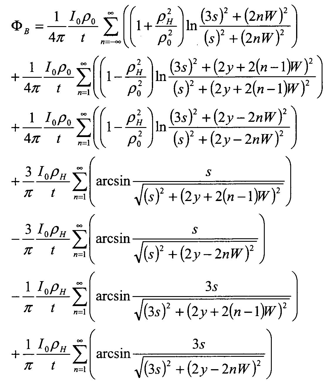
(y=YB1) 및 (y=YB1+W)이 되도록 서로의 사이에 거리 W를 두고 배치된 x-축에 대해 각각 평행한 2개의 경계에 대하여, 그리고 경계들 내에 전류 소스가 배치되면, 정전기장(electrostatic field)은 비섭동 포인트 소스와 2개의 변경된 이미지 전위들의 합계가 될 것이다. 변경된 이미지 전위들은 또한 각각 비섭동 포인트 소스들과 동일한 종류로 된 통상의 미러 전위를 갖는다. 정확한 정전위는 변경된 및 통상의 미러 소스들의 무한(infinite) 합계로 된다.For two boundaries, each parallel to the x-axis arranged at a distance W between each other such that (y = Y B1 ) and (y = Y B1 + W), and within the boundaries The electrostatic field will be the sum of the non-perturbed point source and the two altered image potentials. The altered image potentials also each have a normal mirror potential of the same kind as the non-perturbed point sources. The exact potential is the infinite sum of the modified and common mirror sources.

도 3은 2개의 경계들(흑색선들) 근처에 배치된 2개의 전류 소스들 및 결과로서 생긴 이미지 공간에서의 통상의 및 변경된 미러 이미지들을 개략적으로 예시한다.3 schematically illustrates a typical and modified mirror images in the resulting image space and two current sources disposed near two boundaries (black lines).
직사각형 테스트 패드Rectangular test pad
테스트 패드 내에 전류를 가두는 직사각형 경계의 경우에, 정전위는 도 4에 예시된 바와 같이 변경된 및 통상의 이미지 전위들의 무한 합계가 된다. 전류 밀도가 이 포인트에서 제로가 될 때 코너에 대한 솔루션(solution)이 구해진다. 그러므로, 전류 소스 및 미러 이미지들은 코너 주위에 대칭적으로 배치되어야 한다.In the case of a rectangular boundary that traps current in the test pad, the potential is an infinite sum of altered and conventional image potentials as illustrated in FIG. When the current density goes to zero at this point, the solution for the corner is found. Therefore, the current source and the mirror images must be placed symmetrically around the corner.
도 4는 직사각형을 형성하는 4개의 경계들(흑색선들) 근처에 배치된 2개의 전류 소스들 및 결과로서 생긴 이미지 공간에서의 통상의 및 변경된 미러 이미지들을 개략적으로 예시한다.4 schematically illustrates typical and modified mirror images in the resulting image space and two current sources disposed near four boundaries (black lines) forming a rectangle.
개념의 증명Proof of concept
등거리의 인라인 마이크로 4-포인트 프로브에 의해 홀 효과 측정들이 수행되었다. 도 5에 예시된 바와 같이, 프로브는 2개의 경계들에 공선적인(collinear) p형 Ge 박막 상에 배치되었고, 박막에 대해 수직인 정자장(static magnetic field)이 인가되었다. 도 6 및 도 7에 정의된 2개의 전극 구성들에서 4-포인트 전압-전류를 측정하는 라인 스캔(line scan)이 수행되었다.Hall effect measurements were performed by equidistant inline micro 4-point probes. As illustrated in FIG. 5, the probe was placed on a collinear p-type Ge thin film at two boundaries, and a static magnetic field perpendicular to the thin film was applied. In the two electrode configurations defined in FIGS. 6 and 7, a line scan measuring four-point voltage-current was performed.
도 5는 실험 설정을 개략적으로 예시한다. 4-포인트 프로브는 1㎛의 스캔 스텝으로 2개의 배리어들 사이에서 y-방향으로 스캔될 수 있다.5 schematically illustrates the experimental setup. The four-point probe can be scanned in the y-direction between the two barriers in a scan step of 1 μm.
도 6 및 도 7은 홀 효과 측정을 위해 이용된 2개의 전극 구성들의 개략도이다.6 and 7 are schematic diagrams of two electrode configurations used for the Hall effect measurement.
등거리의 인라인 4-포인트 프로브에 대한 B 구성(도 6)의 정전위는 수학식 23으로 도시될 수 있다.The potential of the B configuration (FIG. 6) for equidistant inline four-point probes can be represented by
여기서, s는 전극 피치이고, 경계들은 (y=0) 및 (y=W)에 배치된다. 도 7에 도시된 B' 구성의 경우, 모든 아크사인(arcsine) 항들은 부호를 변경한다. 그러므로, 2개의 구성들 간의 차는 수학식 24로 주어진다.Where s is the electrode pitch and the boundaries are placed at (y = 0) and (y = W). For the B 'configuration shown in FIG. 7, all arcsine terms change sign. Therefore, the difference between the two configurations is given by equation (24).

홀 저항은 수학식 25로서 정의한다.Hall resistance is defined as Equation (25).
![]()
![]()
그리고 4-포인트 저항은 수학식 26으로서 정의한다.And the four-point resistance is defined as Equation 26.
![]()
![]()
도 8은 구성들 B 및 B'을 이용하여 p형 Ge의 100㎛ 폭의 라인(wide line) 상에서 측정된 4-포인트 저항을 도시하며, 도 9는 계산된 홀 저항을 도시한다. 수학식 23 및 24는 시트 저항, 캐리어 타입, 시트 캐리어 밀도 및 캐리어 이동도를 결정하는 데 이용되었다.FIG. 8 shows the 4-point resistance measured on a 100 μm wide line of p-type Ge using configurations B and B ′, and FIG. 9 shows the calculated Hall resistance.
도 8은 수학식 23의 4-포인트 저항 측정 데이터 및 도표를 개략적으로 예시한다.8 schematically illustrates a four-point resistance measurement data and diagram of
도 9는 도 8의 측정 데이터 및 수학식 24의 도표로부터 계산된 홀 저항을 개략적으로 예시한다.FIG. 9 schematically illustrates the Hall resistance calculated from the measurement data of FIG. 8 and the plot of Equation 24. FIG.
분석 결과들을 확인하기 위해 FEM 시뮬레이션들이 수행되었다. 스캐터링 팩터(scattering factor)가 1인 것으로 가정하면, 시트 저항, 시트 캐리어 밀도 및 캐리어 이동도는 구해지고, 표 1에 도시된다. 표 1은 추출되거나 계산된 재료 특성들의 예들을 도시한다.FEM simulations were performed to confirm the analysis results. Assuming a scattering factor of 1, sheet resistance, sheet carrier density and carrier mobility are obtained and shown in Table 1. Table 1 shows examples of material properties extracted or calculated.

Claims (20)
상기 방법은 평면형(planer) 프로브 표면을 갖는 프로브 몸체 및 상기 평면형 프로브 표면에 평행하게 상기 프로브 몸체로부터 연장하는 제1 다수의 프로브 암을 포함하는 테스트 프로브의 이용 - 상기 프로브는 각각의 프로브 암에 의해 각각 지지되는 제1 다수의 전기 도전성 팁을 더 포함하고, 상기 전기 도전성 팁들은 상기 테스트 영역에의 전기적 접촉을 확립하도록 구성됨 - 을 포함하고,
상기 방법은,
상기 테스트 영역을 수직으로 통과하는 자기력 선들(field lines)을 갖는 자기장(magnetic field)을 제공하는 단계,
상기 프로브를 상기 테스트 영역 상의 제1 위치로 운반하는 단계 ― 상기 제1 다수의 전기 도전성 팁은 상기 테스트 영역과 접촉하고 있음 ―,
각각의 상기 제1 다수의 전기 도전성 팁과 상기 경계 사이의 최단 거리를 결정하는 단계,
각각의 상기 제1 다수의 전기 도전성 팁 사이의 거리들을 결정하는 단계,
전류 소스가 될 하나의 전기 도전성 팁을 선택하는 단계 ― 상기 하나의 전기 도전성 팁은 상기 하나의 전기 도전성 팁이 상기 테스트 샘플의 전압을 결정하기 위해 이용되는 제1 및 제2 전기 도전성 팁 사이에 위치되도록 선택됨 ―,
상기 하나의 전기 도전성 팁과 상기 경계의 상기 최단 거리와, 상기 제1 및 제2 전기 도전성 팁 사이의 거리 사이의 비율(ratio)이 변화되는 일련의 측정들을 수행하는 단계, 및
상기 일련의 측정들에 기초하여 상기 도전성 테스트 영역의 전기적 특성을 계산하는 단계
를 포함하는 방법.A method of determining electrical characteristics of a test sample by using a so-called Hall effect, wherein the test sample comprises a nonconductive region and a test region, wherein the test region is a conductive or semiconductive test region, and the nonconductive region And a boundary is defined between the test region and
The method comprises using a test probe comprising a probe body having a planar probe surface and a first plurality of probe arms extending from the probe body parallel to the planar probe surface, the probes being defined by respective probe arms. Further comprising a first plurality of electrically conductive tips, each supported, wherein the electrically conductive tips are configured to establish electrical contact with the test region;
The method comprises:
Providing a magnetic field having magnetic field lines vertically passing through the test area,
Conveying the probe to a first position on the test region, wherein the first plurality of electrically conductive tips are in contact with the test region;
Determining a shortest distance between each of the first plurality of electrically conductive tips and the boundary,
Determining the distances between each of the first plurality of electrically conductive tips,
Selecting one electrically conductive tip to be a current source, the one electrically conductive tip positioned between the first and second electrically conductive tips wherein the one electrically conductive tip is used to determine the voltage of the test sample Selected to ―,
Performing a series of measurements in which the ratio between the shortest distance of the one electrically conductive tip and the boundary and the distance between the first and second electrically conductive tips is varied, and
Calculating electrical characteristics of the conductive test region based on the series of measurements
How to include.
상기 일련의 측정들은 다수의 동일하지 않은 위치들에서 수행된 측정들에 의해 구성되는 방법.The method of claim 1,
Wherein the series of measurements is constituted by measurements performed at a number of unequal positions.
상기 일련의 측정들은 상이한 전기 도전성 팁을 각 측정에 대한 전류 소스로서 이용함으로써 수행된 측정들에 의해 구성되는 방법.The method of claim 1,
Wherein the series of measurements is constituted by measurements performed by using a different electrically conductive tip as the current source for each measurement.
상기 경계는 선형, 직사각형, 박스형, 정사각형, 삼각형, 원형, 다각형, 임의의 형상, 또는 이들의 임의의 조합인 방법.4. The method according to any one of claims 1 to 3,
The boundary is linear, rectangular, boxed, square, triangular, circular, polygonal, any shape, or any combination thereof.
상기 자기장은 고정적이거나, 또는 대안적으로, 상기 자기장은 가변적인 방법.The method according to any one of claims 1 to 4,
The magnetic field is fixed, or alternatively, the magnetic field is variable.
상기 자기장은 400 mT - 600 mT 등의 200 mT - 700 mT 정도, 바람직하게는 약 500 mT의 필드 세기(field strength)를 갖는 방법.The method of claim 5,
The magnetic field has a field strength of about 200 mT-700 mT, preferably about 500 mT, such as 400 mT-600 mT.
상기 제1 다수의 프로브 팁은 라인 상에 위치되는 방법.The method according to any one of claims 1 to 6,
And the first plurality of probe tips are positioned on a line.
상기 측정들 동안, 상기 프로브는 상기 프로브 팁들이 상기 경계의 일부와 평행하게 위치되도록 배향되는 방법.The method of claim 7, wherein
During the measurements, the probe is oriented such that the probe tips are positioned parallel to a portion of the boundary.
상기 측정들 동안, 상기 프로브는 상기 프로브 팁들이 상기 경계의 일부와 평행하게 위치되도록 배향되는 방법.The method of claim 7, wherein
During the measurements, the probe is oriented such that the probe tips are positioned parallel to a portion of the boundary.
상기 동일하지 않은 위치들은, 상기 전기 도전성 팁들이 상기 도전성 테스트 영역과 접촉하는 동안, 상기 프로브를 하나의 위치로부터 다른 위치로 이동시킴으로써 도달되는 방법.The method according to any one of claims 2 to 9,
The unequal positions are reached by moving the probe from one position to another while the electrically conductive tips are in contact with the conductive test region.
상기 동일하지 않은 위치들은, 상기 전기 도전성 팁들이 새로운 위치에서 상기 도전성 테스트 영역과 접촉하기 전에, 상기 프로브 암들을 상기 도전성 테스트 영역과 접촉하지 않게 이동시키고, 상기 도전 테스트 영역에 대해 상기 프로브를 이동시킴으로써 도달되는 방법.The method according to any one of claims 2 to 9,
The non-identical positions may be determined by moving the probe arms out of contact with the conductive test region and moving the probe relative to the conductive test region before the electrically conductive tips contact the conductive test region at the new position. Method reached.
상기 전기적 특성은 시트 저항 및/또는 액티브 임플란트 도즈 및/또는 캐리어 이동도인 방법.The method according to any one of claims 1 to 11,
Wherein said electrical property is sheet resistance and / or active implant dose and / or carrier mobility.
상기 측정들은 데이터 모델에 맞추어지는 방법.The method according to any one of claims 1 to 12,
Wherein the measurements are fitted to a data model.
상기 방법은 상기 측정을 이론적 데이터에 맞추기 위한 정정 계수 또는 정정 함수를 계산하는 단계를 더 포함하는 방법.The method according to any one of claims 1 to 13,
The method further includes calculating a correction coefficient or a correction function for fitting the measurement to theoretical data.
상기 테스트 영역은 상기 측정들 및 상기 계산들이 무한 시트 계산들을 위한 수학식(equation)들을 이용하여 수행되도록 하는 크기를 정의하는 방법.The method according to any one of claims 1 to 14,
Wherein said test area defines a size such that said measurements and said calculations are performed using equations for infinite sheet calculations.
상기 방법은 유한 요소법과 같은 수치법(numerical method)을 이용하는 단계를 포함하는 방법.The method according to any one of claims 1 to 15,
The method includes using a numerical method such as a finite element method.
상기 방법은 평면형 프로브 표면을 갖는 프로브 몸체 및 상기 평면형 프로브 표면에 평행하게 상기 프로브 몸체로부터 연장하는 4개의 프로브 암들을 포함하는 테스트 프로브의 이용 ― 상기 프로브는 각각의 프로브 암에 의해 각각 지지되는 4개의 전기 도전성 팁들을 더 포함하고, 상기 전기 도전성 팁들은 상기 테스트 영역에의 전기적 접촉을 확립하도록 구성됨 ― 을 포함하고,
상기 방법은,
상기 도전성 테스트 영역에 수직인 자기장을 제공하는 단계,
상기 프로브를 상기 도전성 테스트 영역 상의 제1 위치로 운반하는 단계 ― 상기 4개의 전기 도전성 팁들은 상기 도전성 테스트 영역과 접촉하고 있음 ―,
상기 경계에 대하여 상기 4개의 전기 도전성 팁들 각각에 대한 위치를 결정하는 단계,
각각의 상기 4개의 전기 도전성 팁들 사이의 거리들을 결정하는 단계,
전류 소스가 될 하나의 전기 도전성 팁을 선택하는 단계 ― 상기 하나의 전기 도전성 팁은, 상기 하나의 전기 도전성 팁이 상기 테스트 샘플의 전압을 결정하기 위해 이용되는 제1 및 제2 전기 도전성 팁 사이에 위치되도록 선택됨 ―,
상기 하나의 전기 도전성 팁에 전류를 인가하고, 상기 제1 및 제2 전기 도전성 팁들에 걸리는 상기 전압을 결정함으로써 제1 측정을 수행하는 단계,
상기 제1 위치로부터 떨어져 있는 제2 위치로 상기 프로브를 이동시키는 단계,
상기 하나의 전기 도전성 팁에 전류를 인가하고, 상기 제1 및 제2 전기 도전성 팁들에 걸리는 상기 전압을 결정함으로써 제2 측정을 수행하는 단계, 및
상기 제1 및 제2 측정에 기초하여, 상기 도전성 테스트 영역의 전기적 특성을 계산하는 단계
를 포함하는 방법. A method of determining electrical characteristics of a test sample by using a so-called Hall effect, wherein the test sample comprises a non-conductive region and a conductive test region, and a boundary defined between the non-conductive region and the conductive test region,
The method uses a test probe comprising a probe body having a planar probe surface and four probe arms extending from the probe body parallel to the planar probe surface, wherein the probes are each supported by each probe arm. Further comprising electrically conductive tips, wherein the electrically conductive tips are configured to establish electrical contact with the test region;
The method comprises:
Providing a magnetic field perpendicular to the conductive test region,
Conveying the probe to a first location on the conductive test region, wherein the four electrically conductive tips are in contact with the conductive test region;
Determining a location for each of the four electrically conductive tips relative to the boundary,
Determining the distances between each of the four electrically conductive tips,
Selecting one electrically conductive tip to be a current source, wherein the one electrically conductive tip is arranged between the first and second electrically conductive tips wherein the one electrically conductive tip is used to determine the voltage of the test sample. Selected to be positioned ―,
Applying a current to the one electrically conductive tip and performing a first measurement by determining the voltage across the first and second electrically conductive tips,
Moving the probe to a second position away from the first position,
Applying a current to the one electrically conductive tip and performing a second measurement by determining the voltage across the first and second electrically conductive tips, and
Calculating electrical characteristics of the conductive test region based on the first and second measurements
How to include.
상기 제1항 내지 제16항 중 어느 한 항의 특징들 중 임의의 특징을 더 포함하는 방법.The method of claim 17 or 18,
17. A method further comprising any of the features of any of the preceding claims.
평면형 프로브 표면을 갖는 프로브 몸체 및 상기 평면형 프로브 표면에 평행하게 상기 프로브 몸체로부터 연장하는 복수의 프로브 암 ― 상기 프로브는 각각의 프로브 암에 의해 지지되는 복수의 전기 도전성 팁을 더 포함하고, 상기 전기 도전성 팁들은 상기 테스트 영역에의 전기적 접촉을 확립하도록 구성되고, 상기 테스트 프로브는 테스트 프로브 홀더에 수용됨 ―,
상기 테스트 샘플을 수용하여 유지하는 테스트 샘플 홀더 ― 상기 테스트 프로브 홀더 및 상기 테스트 샘플 홀더는 서로에 대해 이동가능함 ―, 및
제1항 내지 제19항 중 어느 한 항에 따른 방법들 중 임의의 방법의 소프트웨어 구현을 포함하는 마이크로프로세서 시스템
을 포함하는 시스템.A system for determining electrical characteristics of a test sample by using a so-called Hall effect, wherein the test sample comprises a non-conductive region and a conductive test region, and a boundary defined between the non-conductive region and the conductive test region,
A probe body having a planar probe surface and a plurality of probe arms extending from the probe body parallel to the planar probe surface, the probes further comprising a plurality of electrically conductive tips supported by respective probe arms; Tips are configured to establish electrical contact to the test area, and the test probe is received in a test probe holder;
A test sample holder for receiving and holding said test sample, said test probe holder and said test sample holder being movable relative to each other, and
A microprocessor system comprising a software implementation of any of the methods according to claim 1.
System comprising.
Applications Claiming Priority (3)
| Application Number | Priority Date | Filing Date | Title |
|---|---|---|---|
| EP07388066.8 | 2007-09-03 | ||
| EP07388066 | 2007-09-03 | ||
| PCT/DK2008/000315 WO2009030230A1 (en) | 2007-09-03 | 2008-09-03 | A method of determining an electrical property of a test sample |
Publications (2)
| Publication Number | Publication Date |
|---|---|
| KR20100049098A true KR20100049098A (en) | 2010-05-11 |
| KR101537121B1 KR101537121B1 (en) | 2015-07-15 |
Family
ID=39929605
Family Applications (1)
| Application Number | Title | Priority Date | Filing Date |
|---|---|---|---|
| KR1020107004788A KR101537121B1 (en) | 2007-09-03 | 2008-09-03 | A method of determining an electrical property of a test sample |
Country Status (7)
| Country | Link |
|---|---|
| US (1) | US8907690B2 (en) |
| EP (1) | EP2198316A1 (en) |
| JP (1) | JP5651469B2 (en) |
| KR (1) | KR101537121B1 (en) |
| CN (1) | CN101821638B (en) |
| IL (1) | IL203966A (en) |
| WO (1) | WO2009030230A1 (en) |
Cited By (3)
| Publication number | Priority date | Publication date | Assignee | Title |
|---|---|---|---|---|
| WO2012086979A1 (en) * | 2010-12-20 | 2012-06-28 | 부산대학교 산학협력단 | Method for manufacturing 4-point probe holder using single crystal and single crystal 4-point probe holder manufactured by same |
| KR20170045230A (en) * | 2014-07-25 | 2017-04-26 | 더 세크러테리 오브 스테이트 포 비즈니스, 이노베이션 & 스킬스 | Measurement technique for thin-film characterization |
| KR20190105041A (en) * | 2017-01-09 | 2019-09-11 | 카프레스 에이/에스 | Position calibration method and system for position calibration for four probe resistance measurements |
Families Citing this family (9)
| Publication number | Priority date | Publication date | Assignee | Title |
|---|---|---|---|---|
| EP2469271A1 (en) * | 2010-12-21 | 2012-06-27 | Capres A/S | Single-position Hall effect measurements |
| EP2656056A1 (en) * | 2010-12-21 | 2013-10-30 | Capres A/S | Single-position hall effect measurements |
| EP2498081A1 (en) * | 2011-03-08 | 2012-09-12 | Capres A/S | Single-position hall effect measurements |
| EP2677324A1 (en) | 2012-06-20 | 2013-12-25 | Capres A/S | Deep-etched multipoint probe |
| DE102017007578A1 (en) * | 2017-08-11 | 2019-02-14 | Forschungszentrum Jülich GmbH | Method and device for determining the electrical resistance of an object |
| US10557897B2 (en) | 2018-01-19 | 2020-02-11 | International Business Machines Corporation | Non-contact conductivity and magnetic susceptibility measurement with parallel dipole line trap system |
| CN108957053A (en) * | 2018-06-23 | 2018-12-07 | 四川峰哲精密设备有限公司 | A kind of test contact chip for testing needle assemblies and its composition |
| CN110031668A (en) * | 2019-05-14 | 2019-07-19 | 重庆大学 | Current measuring device based on TMR tunnel magnetoresistive |
| US11740279B2 (en) | 2020-04-24 | 2023-08-29 | Kla Corporation | Measuring temperature-modulated properties of a test sample |
Family Cites Families (26)
| Publication number | Priority date | Publication date | Assignee | Title |
|---|---|---|---|---|
| US3456186A (en) * | 1966-10-31 | 1969-07-15 | Collins Radio Co | Circuit for measuring sheet resistivity including an a.c. current source and average reading d.c. voltmeter switchably connected to pairs of a four probe array |
| DD110981A1 (en) | 1974-05-08 | 1975-01-12 | ||
| JPS5262479A (en) | 1975-11-19 | 1977-05-23 | Agency Of Ind Science & Technol | Prove device for measurement |
| DE2726982A1 (en) | 1977-06-15 | 1979-01-04 | Egbert Prof Dr Ing Hesse | Thin semiconductor sample or film resistivity measurement - using four contacts placed in a circle on sample at certain min. distances from each other and from the edge of sample |
| US4703252A (en) | 1985-02-22 | 1987-10-27 | Prometrix Corporation | Apparatus and methods for resistivity testing |
| US4864227A (en) * | 1987-02-27 | 1989-09-05 | Canon Kabushiki Kaisha | Wafer prober |
| US5084671A (en) * | 1987-09-02 | 1992-01-28 | Tokyo Electron Limited | Electric probing-test machine having a cooling system |
| US4857839A (en) * | 1988-03-02 | 1989-08-15 | Wright State University | Method and apparatus for measuring average resistivity and hall-effect of semiconductor wafers |
| CH682017A5 (en) * | 1990-02-01 | 1993-06-30 | Radivoje Popovic | Appts. for measuring characteristic values of semiconductor wafer - employs homogeneous magnetic field and predefined test current to establish specific resistance and Hall coefft. of sample |
| US5150042A (en) * | 1991-09-23 | 1992-09-22 | The United States Of America As Represented By The Secretary Of The Air Force | On-wafer Hall-effect measurement system |
| DE4231392A1 (en) | 1992-09-19 | 1994-03-24 | Daimler Benz Ag | Method for determining the electronic properties of semiconductor layer structures |
| US5691648A (en) | 1992-11-10 | 1997-11-25 | Cheng; David | Method and apparatus for measuring sheet resistance and thickness of thin films and substrates |
| US5500589A (en) * | 1995-01-18 | 1996-03-19 | Honeywell Inc. | Method for calibrating a sensor by moving a magnet while monitoring an output signal from a magnetically sensitive component |
| US5789931A (en) * | 1995-10-04 | 1998-08-04 | The United States Of America As Represented By The Secretary Of The Navy | Quantitative mobility spectrum analysis for magnetic field dependent hall and resistivity data |
| WO1998044360A2 (en) * | 1997-04-01 | 1998-10-08 | Redcliffe Magtronics Ltd. | An apparatus and method of measuring the magnetic field distribution of a magnetic sample |
| US6064202A (en) * | 1997-09-09 | 2000-05-16 | Physical Electronics Laboratory | Spinning current method of reducing the offset voltage of a hall device |
| US6100704A (en) * | 1998-04-30 | 2000-08-08 | The United States Of America As Represented By The Secretary Of The Navy | Quantitative mobility spectrum analysis of magnetic-field dependent hall and resistivity data |
| JP2001244308A (en) * | 2000-02-25 | 2001-09-07 | Mitsubishi Electric Corp | Probe for high frequency signal |
| US6747445B2 (en) | 2001-10-31 | 2004-06-08 | Agere Systems Inc. | Stress migration test structure and method therefor |
| US6943571B2 (en) | 2003-03-18 | 2005-09-13 | International Business Machines Corporation | Reduction of positional errors in a four point probe resistance measurement |
| US7078919B2 (en) * | 2003-08-27 | 2006-07-18 | Prussin Simon A | In situ determination of resistivity, mobility and dopant concentration profiles |
| KR100608656B1 (en) | 2003-09-20 | 2006-08-04 | 엘지전자 주식회사 | Velocity control apparatus for motor |
| US7009414B2 (en) | 2003-10-17 | 2006-03-07 | International Business Machines Corporation | Atomic force microscope and method for determining properties of a sample surface using an atomic force microscope |
| US7034519B2 (en) | 2004-01-08 | 2006-04-25 | International Business Machines Corporation | High frequency measurement for current-in-plane-tunneling |
| US7474114B2 (en) * | 2005-09-08 | 2009-01-06 | Sitronic Corporation | System and method for characterizing silicon wafers |
| US7626377B2 (en) * | 2008-02-18 | 2009-12-01 | Honeywell International Inc. | Hall-effect device with merged and/or non-merged complementary structure |
-
2008
- 2008-09-03 CN CN200880110546.5A patent/CN101821638B/en active Active
- 2008-09-03 WO PCT/DK2008/000315 patent/WO2009030230A1/en active Application Filing
- 2008-09-03 US US12/676,124 patent/US8907690B2/en active Active
- 2008-09-03 JP JP2010523276A patent/JP5651469B2/en active Active
- 2008-09-03 EP EP08784438A patent/EP2198316A1/en not_active Withdrawn
- 2008-09-03 KR KR1020107004788A patent/KR101537121B1/en active IP Right Grant
-
2010
- 2010-02-15 IL IL203966A patent/IL203966A/en active IP Right Grant
Cited By (3)
| Publication number | Priority date | Publication date | Assignee | Title |
|---|---|---|---|---|
| WO2012086979A1 (en) * | 2010-12-20 | 2012-06-28 | 부산대학교 산학협력단 | Method for manufacturing 4-point probe holder using single crystal and single crystal 4-point probe holder manufactured by same |
| KR20170045230A (en) * | 2014-07-25 | 2017-04-26 | 더 세크러테리 오브 스테이트 포 비즈니스, 이노베이션 & 스킬스 | Measurement technique for thin-film characterization |
| KR20190105041A (en) * | 2017-01-09 | 2019-09-11 | 카프레스 에이/에스 | Position calibration method and system for position calibration for four probe resistance measurements |
Also Published As
| Publication number | Publication date |
|---|---|
| US20100271059A1 (en) | 2010-10-28 |
| JP5651469B2 (en) | 2015-01-14 |
| EP2198316A1 (en) | 2010-06-23 |
| IL203966A (en) | 2014-08-31 |
| WO2009030230A1 (en) | 2009-03-12 |
| CN101821638B (en) | 2014-09-03 |
| CN101821638A (en) | 2010-09-01 |
| JP2010540890A (en) | 2010-12-24 |
| KR101537121B1 (en) | 2015-07-15 |
| US8907690B2 (en) | 2014-12-09 |
Similar Documents
| Publication | Publication Date | Title |
|---|---|---|
| KR101537121B1 (en) | A method of determining an electrical property of a test sample | |
| Petersen et al. | Micro-four-point probe Hall effect measurement method | |
| Perkins et al. | Surface-sensitive conductivity measurement using a micro multi-point probe approach | |
| JP5744401B2 (en) | Measuring method of sheet resistance and leakage current density of shallow semiconductor implantation | |
| Kjeldby et al. | Probing dimensionality using a simplified 4-probe method | |
| JP2005303321A (en) | Method for inspecting semiconductor wafer by non-penetration probe | |
| US20210333316A1 (en) | Measuring Temperature-Modulated Properties of a Test Sample | |
| Hansen et al. | Resolution enhancement of scanning four-point-probe measurements on two-dimensional systems | |
| US20210333228A1 (en) | Micro-Four-Point Metrology of Joule-Heating-Induced Modulation of Test Sample Properties | |
| US6208154B1 (en) | Method of determining the doping concentration across a surface of a semiconductor material | |
| Wang et al. | Sensitivity study of micro four-point probe measurements on small samples | |
| Wells et al. | Surface-sensitive conductance measurements on clean and stepped semiconductor surfaces: Numerical simulations of four point probe measurements | |
| Lozanova et al. | A three-point-probe method for measuring resistivity and the Hall coefficient using Hall devices with minimal design complexity | |
| EP2871487A1 (en) | Small scale measurements of anisotropic sheet conductances | |
| Kjaer et al. | Characterization of positional errors and their influence on micro four-point probe measurements on a 100 nm Ru film | |
| Nikolov et al. | Virtual System for Sheet Resistance Measurement of Inkjet Printed Conductive Layers | |
| Benjamin et al. | Ultra-shallow junction (USJ) sheet resistance measurements with a non-penetrating four point probe | |
| Szymański et al. | An Enhancement of the Van Der Pauw Method | |
| Petersen et al. | High precision micro-scale Hall effect characterization method using in-line micro four-point probes | |
| Křivka et al. | Resistivity mapping: An example of aged conducting polymer | |
| Cannon | Electroquasistatic sensors for surface and subsurface nano-imaging of integrated circuit features | |
| Burtscher et al. | Electrical measurement of resistivity fluctuations associated with striations in silicon crystals | |
| Osterberg et al. | Accurate micro Hall Effect measurements on scribe line pads | |
| Witthøft | Micro Four-Point Probe based Metrology | |
| Witthøft et al. | Precision of Micro Hall Effect Measurements in Scribe Line Test Pads |
Legal Events
| Date | Code | Title | Description |
|---|---|---|---|
| A201 | Request for examination | ||
| E902 | Notification of reason for refusal | ||
| E90F | Notification of reason for final refusal | ||
| E701 | Decision to grant or registration of patent right | ||
| GRNT | Written decision to grant | ||
| FPAY | Annual fee payment |
Payment date: 20180626 Year of fee payment: 4 |
|
| FPAY | Annual fee payment |
Payment date: 20190611 Year of fee payment: 5 |