KR20090076806A - Scanning exposure apparatus and device manufacturing method - Google Patents
Scanning exposure apparatus and device manufacturing method Download PDFInfo
- Publication number
- KR20090076806A KR20090076806A KR1020090000605A KR20090000605A KR20090076806A KR 20090076806 A KR20090076806 A KR 20090076806A KR 1020090000605 A KR1020090000605 A KR 1020090000605A KR 20090000605 A KR20090000605 A KR 20090000605A KR 20090076806 A KR20090076806 A KR 20090076806A
- Authority
- KR
- South Korea
- Prior art keywords
- center position
- exposure
- scanning
- light
- blades
- Prior art date
Links
Images


Classifications
-
- G—PHYSICS
- G03—PHOTOGRAPHY; CINEMATOGRAPHY; ANALOGOUS TECHNIQUES USING WAVES OTHER THAN OPTICAL WAVES; ELECTROGRAPHY; HOLOGRAPHY
- G03F—PHOTOMECHANICAL PRODUCTION OF TEXTURED OR PATTERNED SURFACES, e.g. FOR PRINTING, FOR PROCESSING OF SEMICONDUCTOR DEVICES; MATERIALS THEREFOR; ORIGINALS THEREFOR; APPARATUS SPECIALLY ADAPTED THEREFOR
- G03F7/00—Photomechanical, e.g. photolithographic, production of textured or patterned surfaces, e.g. printing surfaces; Materials therefor, e.g. comprising photoresists; Apparatus specially adapted therefor
- G03F7/70—Microphotolithographic exposure; Apparatus therefor
- G03F7/70216—Mask projection systems
- G03F7/70358—Scanning exposure, i.e. relative movement of patterned beam and workpiece during imaging
-
- G—PHYSICS
- G03—PHOTOGRAPHY; CINEMATOGRAPHY; ANALOGOUS TECHNIQUES USING WAVES OTHER THAN OPTICAL WAVES; ELECTROGRAPHY; HOLOGRAPHY
- G03B—APPARATUS OR ARRANGEMENTS FOR TAKING PHOTOGRAPHS OR FOR PROJECTING OR VIEWING THEM; APPARATUS OR ARRANGEMENTS EMPLOYING ANALOGOUS TECHNIQUES USING WAVES OTHER THAN OPTICAL WAVES; ACCESSORIES THEREFOR
- G03B27/00—Photographic printing apparatus
- G03B27/32—Projection printing apparatus, e.g. enlarger, copying camera
- G03B27/52—Details
- G03B27/54—Lamp housings; Illuminating means
-
- G—PHYSICS
- G03—PHOTOGRAPHY; CINEMATOGRAPHY; ANALOGOUS TECHNIQUES USING WAVES OTHER THAN OPTICAL WAVES; ELECTROGRAPHY; HOLOGRAPHY
- G03F—PHOTOMECHANICAL PRODUCTION OF TEXTURED OR PATTERNED SURFACES, e.g. FOR PRINTING, FOR PROCESSING OF SEMICONDUCTOR DEVICES; MATERIALS THEREFOR; ORIGINALS THEREFOR; APPARATUS SPECIALLY ADAPTED THEREFOR
- G03F7/00—Photomechanical, e.g. photolithographic, production of textured or patterned surfaces, e.g. printing surfaces; Materials therefor, e.g. comprising photoresists; Apparatus specially adapted therefor
- G03F7/70—Microphotolithographic exposure; Apparatus therefor
- G03F7/70058—Mask illumination systems
- G03F7/70066—Size and form of the illuminated area in the mask plane, e.g. reticle masking blades or blinds
-
- G—PHYSICS
- G03—PHOTOGRAPHY; CINEMATOGRAPHY; ANALOGOUS TECHNIQUES USING WAVES OTHER THAN OPTICAL WAVES; ELECTROGRAPHY; HOLOGRAPHY
- G03F—PHOTOMECHANICAL PRODUCTION OF TEXTURED OR PATTERNED SURFACES, e.g. FOR PRINTING, FOR PROCESSING OF SEMICONDUCTOR DEVICES; MATERIALS THEREFOR; ORIGINALS THEREFOR; APPARATUS SPECIALLY ADAPTED THEREFOR
- G03F7/00—Photomechanical, e.g. photolithographic, production of textured or patterned surfaces, e.g. printing surfaces; Materials therefor, e.g. comprising photoresists; Apparatus specially adapted therefor
- G03F7/70—Microphotolithographic exposure; Apparatus therefor
- G03F7/70058—Mask illumination systems
- G03F7/70141—Illumination system adjustment, e.g. adjustments during exposure or alignment during assembly of illumination system
-
- G—PHYSICS
- G03—PHOTOGRAPHY; CINEMATOGRAPHY; ANALOGOUS TECHNIQUES USING WAVES OTHER THAN OPTICAL WAVES; ELECTROGRAPHY; HOLOGRAPHY
- G03F—PHOTOMECHANICAL PRODUCTION OF TEXTURED OR PATTERNED SURFACES, e.g. FOR PRINTING, FOR PROCESSING OF SEMICONDUCTOR DEVICES; MATERIALS THEREFOR; ORIGINALS THEREFOR; APPARATUS SPECIALLY ADAPTED THEREFOR
- G03F7/00—Photomechanical, e.g. photolithographic, production of textured or patterned surfaces, e.g. printing surfaces; Materials therefor, e.g. comprising photoresists; Apparatus specially adapted therefor
- G03F7/70—Microphotolithographic exposure; Apparatus therefor
- G03F7/70483—Information management; Active and passive control; Testing; Wafer monitoring, e.g. pattern monitoring
- G03F7/70491—Information management, e.g. software; Active and passive control, e.g. details of controlling exposure processes or exposure tool monitoring processes
- G03F7/70516—Calibration of components of the microlithographic apparatus, e.g. light sources, addressable masks or detectors
Landscapes
- Physics & Mathematics (AREA)
- General Physics & Mathematics (AREA)
- Exposure And Positioning Against Photoresist Photosensitive Materials (AREA)
- Exposure Of Semiconductors, Excluding Electron Or Ion Beam Exposure (AREA)
Abstract
Description
본 발명은 주사노광장치 및 그것을 사용하여 디바이스를 제조하는 디바이스의 제조방법에 관한 것이다.The present invention relates to a scanning exposure apparatus and a method for manufacturing a device using the same.
웨이퍼 상에 회로패턴을 형성하는 방법으로서 리소그래피법이 잘 알려져 있다. 이 리소그래피법에서는, 회로패턴이 형성된 레티클의 패턴이 웨이퍼에 투영되어 상기 웨이퍼가 노광된다. 웨이퍼에는 감광제가 도포되어 있고, 웨이퍼의 노광에 의해 상기 감광제에 잠상이 형성된다. 이 잠상은 현상공정에 의해 물리적인 패턴이 된다.The lithographic method is well known as a method of forming a circuit pattern on a wafer. In this lithography method, a pattern of a reticle on which a circuit pattern is formed is projected onto a wafer to expose the wafer. The photosensitive agent is apply | coated to the wafer, and the latent image is formed in the said photosensitive agent by exposure of a wafer. This latent image becomes a physical pattern by the developing process.
반도체 디바이스의 제조공정의 웨이퍼 프로세스에서는, 웨이퍼 표면의 산화공정, 절연막 형성공정, 전극의 증착공정, 이온주입공정, 및 에칭공정을 반복함으로써 회로패턴이 형성된다. 이 웨이퍼프로세스에 있어서, 절연막의 두께나 노광공정에서의 감광제의 두께가 불균일하게 되는 경우가 있다. 이 경우에서와 같이 절연막의 두께나 감광제의 두께가 불균일하게 형성된 웨이퍼를 노광하면, 패턴 선폭의 시프트나 해상의 불량이 발생되어, 제품의 수율이 저하된다. 특히, 일반적으로 쇼 트영역이 비교적 넓은 스텝 앤드 스캔 노광장치에서는, 쇼트영역 내에 있어서의 두께가 상당히 불균일하게 되어 무시할 수 없는 해상 불량이 발생된다.In the wafer process of the semiconductor device manufacturing process, a circuit pattern is formed by repeating the oxidation process of the wafer surface, the insulating film formation process, the electrode deposition process, the ion implantation process, and the etching process. In this wafer process, the thickness of an insulating film and the thickness of the photosensitive agent in an exposure process may become nonuniform. As in this case, exposure of a wafer in which the thickness of the insulating film and the thickness of the photosensitive agent are unevenly exposed causes a shift in the pattern line width and a poor resolution, resulting in a decrease in the yield of the product. In particular, in a step-and-scan exposure apparatus having a relatively large short region, the thickness in the short region becomes substantially nonuniform, resulting in an insignificant resolution defect.
일본국 특개평 7-29810호 공보에는, 노광빔에 의한 기판의 노광량을 기판 상의 위치에 따라 변경하는 것과, 조도, 펄스 발광광원의 펄스발광의 시간간격, 및 스테이지의 주사속도를 변경하는 것에 의해 문제를 해결하는 것이 개시되어 있다.Japanese Laid-Open Patent Publication No. 7-29810 discloses that the exposure amount of the substrate by the exposure beam is changed in accordance with the position on the substrate, and the illuminance, the time interval of pulse emission of the pulsed light source, and the scanning speed of the stage are changed. Solving the problem is disclosed.
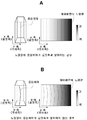
도 1은 웨이퍼에 입사하는 노광광의 강도를 예시하는 도면이다. 주사 노광에 있어서는, 웨이퍼스테이지를 주사축방향으로 이동시키면서, 광원의 발광을 반복함으로써 웨이퍼가 노광된다.1 is a diagram illustrating the intensity of exposure light incident on a wafer. In scanning exposure, the wafer is exposed by repeating light emission of the light source while moving the wafer stage in the scanning axis direction.
노광광의 중심 위치란, 도 1에 도시된 바와 같이, 주사축방향에 있어서의 광강도분포의 중심위치이며, 각 상높이(슬릿축방향에 있어서의 각 위치) 마다 구해진다. 본 명세서에서는, 상높이 마다의 중심 위치를 가상적으로 연결한 곡선을 중심선이라고 부른다.As shown in FIG. 1, the center position of exposure light is a center position of the light intensity distribution in the scanning axis direction, and is obtained for each image height (each position in the slit axis direction). In this specification, the curve which virtually connected the center position for every image height is called center line.
일본국 특개평7-29810호 공보에 기재된 방법에 따라 노광량을 변화시키면, 주사노광 후의 노광량(노광광의 강도를 시간으로 적분한 값)의 변화는 도 2A 및 도 2B에 예시한 바와 같이 중심선의 만곡에 의존한다. 도 2A 및 도 2B의 예에서는, 주사축방향에 대해서, 노광광의 강도를 1차 함수적으로 증가시키고 있다.When the exposure amount is changed in accordance with the method described in Japanese Patent Laid-Open No. 7-29810, the change in the exposure amount (the value obtained by integrating the intensity of exposure light with time) after scanning exposure is curvature of the center line as illustrated in FIGS. 2A and 2B. Depends on In the example of FIGS. 2A and 2B, the intensity of the exposure light is linearly increased in the scanning axis direction.
도 2A는 노광광의 중심선이 슬릿축에 평행한 예이다. 도 2B는 노광광의 중심선이 만곡하고 있는 예이다. 도 2A 및 도 2B를 참조하면, 주사 노광된 쇼트영역의 노광량은, 노광광의 중심선의 만곡에 의존한 불균일성을 나타낸다. 따라서, 주사축방향의 위치에 따라서 노광광의 강도를 변화시키는 경우에는, 노광광의 중심선을 노광광 프로파일에 따라서 조정해야 하는 것이다. 또한, 이 중심선의 바람직한 형상은 수반된 환경에 따라 직선일 수도 있고, 또는 제어된 곡선일 수도 있다.2A is an example in which the center line of exposure light is parallel to the slit axis. 2B is an example in which the centerline of the exposure light is curved. Referring to Figs. 2A and 2B, the exposure amount of the shot-exposed shot region shows nonuniformity depending on the curvature of the center line of the exposure light. Therefore, when changing the intensity of exposure light in accordance with the position in the scanning axis direction, it is necessary to adjust the centerline of the exposure light in accordance with the exposure light profile. In addition, the preferred shape of this centerline may be a straight line or a controlled curve depending on the environment involved.
본 발명은, 예를 들면, 쇼트영역 내의 노광량을 보다 고정밀도로 제어하기 위해 적합한 기술을 제공한다.The present invention provides, for example, a technique suitable for more precisely controlling the exposure amount in the shot region.
본 발명의 하나의 측면에 의하면, 원판 및 기판을 주사하면서 상기 원판의 패턴을 투영광학계에 의해 상기 기판에 투영해서 상기 기판을 주사 노광하는 주사노광장치로서, 상기 장치는 상기 투영광학계의 상면을 조사하는 노광광의 주사축방향에 있어서의 중심위치를 목표중심 위치에 의거해서 조정하는 중심위치 조정유닛을 구비한 주사노광장치를 제공한다.According to one aspect of the present invention, a scanning exposure apparatus for scanning and exposing the substrate by projecting the pattern of the original plate onto the substrate by a projection optical system while scanning the original plate and the substrate, the apparatus irradiating an upper surface of the projection optical system A scanning exposure apparatus provided with a center position adjusting unit for adjusting a center position of the exposure light in the scanning axis direction based on a target center position.
본 발명의 다른 측면에 의하면, 주사노광장치를 사용하여 기판을 노광하는 공정 및 상기 기판을 현상하는 공정을 포함하는 디바이스의 제조방법을 제공한다.상기 주사노광장치는 원판 및 기판을 주사하면서 상기 원판의 패턴을 투영광학계에 의해 상기 기판에 투영하고 이에 의해 상기 기판을 주사 노광한다. 상기 노광장치는 상기 투영광학계의 상면에 입사하는 노광광의 주사축 방향에 있어서의 중심위치를 목표중심 위치에 의거하여 조정하는 중심위치 조정유닛을 구비한다.According to another aspect of the present invention, there is provided a device manufacturing method comprising a step of exposing a substrate using a scanning exposure apparatus and a step of developing the substrate. The scanning exposure apparatus scans the master and the substrate while scanning the master. Is projected onto the substrate by a projection optical system, thereby scanning the substrate. The exposure apparatus includes a center position adjusting unit that adjusts the center position in the scanning axis direction of the exposure light incident on the image plane of the projection optical system based on the target center position.
본 발명의 다른 특징은 첨부도면을 참조한 다음의 전형적인 실시형태의 설명으로부터 명백해질 것이다. Other features of the present invention will become apparent from the following description of exemplary embodiments with reference to the accompanying drawings.
이하, 첨부 도면을 참조하면서 본 발명의 전형적인 실시형태를 설명한다.EMBODIMENT OF THE INVENTION Hereinafter, typical embodiment of this invention is described, referring an accompanying drawing.
도 3은 본 발명의 전형적인 실시형태의 주사노광장치의 개략구성을 나타내는 블럭도이다. 도 3을 참조하면, 레이저(광원)(1)에 의해 방사된 광(펄스광)은 빔정형광학계(2)를 통과해서 소정의 단면 형상으로 정형되어 옵티컬인티그레이터(3)에 입사한다. 옵티컬인티그레이터(3)는 복수의 미소한 렌즈를 포함하고 있고 그 출사면측에 복수의 2차 광원을 형성한다.3 is a block diagram showing a schematic configuration of a scanning exposure apparatus of a typical embodiment of the present invention. Referring to FIG. 3, light (pulse light) emitted by the laser (light source) 1 passes through the beam shaping
조리개 터릿(4)은 회전판에 복수의 조리개를 구성함으로써 형성된다. 선택된 조리개가 광로에 삽입되고, 이에 의해 상술한 복수의 2차 광원이 형성된 영역으로부터 필요한 영역이 추출된다. 복수의 조리개의 예로서는, 코히런스팩터(σ)의 값을 설정하기 위한 원형 개구면적이 상이한 복수의 개구조리개나, 윤대조명용의 링형상조리개, 및 4중극조리개가 있다.The
제1광전변환장치(6)는 하프미러(5)에 의해 반사된 광의 성분의 일부를 펄스당의 광량으로서 검출해서, 그 검출결과를 노광량 연산부(21)에 출력한다.The first
콘덴서렌즈(7)는 옵티컬 인티그레이터(3)의 출사면측에 형성된 복수의 2차 광원으로부터의 광에 의해 마스킹블레이드(9)를 조명한다. 마스킹블레이드(9)의 근방에는 가변슬릿(8)이 배치되어 있고, 마스킹 블레이드(9)를 조명하는 광의 프로파일을 슬릿형상(예를 들면, 직사각형 또는 원호형상)으로 형성한다. 마스킹블레이드(9)의 개구영역을 통과한 광은, 콘덴서렌즈(10)와 미러(11)를 개재하여, 마스킹블레이드(9)가 배치된 면과 공역인 면에 배치된 레티클(원판)(13)의 면에 조도와 입사각도가 균일화된 상태로 결상한다. 광학 배율비에 있어서 마스킹블레이드(9)의 개구영역은 레티클(13)의 조명영역과 유사하다.The
레티클(13)은 레티클스테이지(14)에 의해 유지된다. 레티클(13)을 통과한 광은 투영광학계(15)를 통과해서 레티클(13)의 패턴면과 광학적으로 공역인 면의 노광 화각영역에 광학상을 다시 형성한다. 포커스검출계(16)는 웨이퍼스테이지(17)에 의해 유지된 웨이퍼(기판)(18)의 표면의 높이나 기울기를 검출한다. 주사 노광시에는, 포커스검출계(16)에 의해 검출된 정보에 의거해서 웨이퍼(18)의 표면이 투영광학계(15)의 상면과 일치하도록 웨이퍼스테이지(17)를 제어하면서, 레티클스테이지(14)와 웨이퍼스테이지(17)가 투영광학계(15)에 대해서 동기해서 주사된다. 이 때, 웨이퍼(18)가 슬릿형상의 광에 의해 상대적으로 주사되어 웨이퍼(18)의 감광제에 레티클(13)의 패턴이 전사된다.The reticle 13 is held by the
웨이퍼스테이지(17) 상에는, 제2광전변환장치(검출기)(19)가 배치되어 있어서 노광화각영역 내에 입사하는 광의 광량을 측정할 수 있다. 제2광전변환장치(검출기)(19)는, 예를 들면, 포토다이오드, 이미지 센서(예를 들면, CCD 이미지 센서), 또는, 라인 센서(예를 들면, CCD 라인 센서)를 포함할 수 있다. 스테이지구동제어계(20)는 도시하지 않은 구동기구에 의해 레티클스테이지(14) 및 웨이퍼스테이지(17)의 구동을 제어한다.On the
제1광전변환장치(6)는 웨이퍼의 노광중에도 노광량의 계측이 가능하다. 제2광전변환장치(19)는 웨이퍼의 노광이 이루어지지 않는 상태에서, 투영광학계(15)의 상면에 결상되는 슬릿형상의 노광광의 광량을 검출한다. 노광량 연산부(21)는, 제1광전변환장치(6)의 출력과 제2광전변환장치(19)의 출력사이의 상관을 구해서 유지한다. 이 상관과 제1광전변환장치(6)의 출력에 의거해서, 노광시에 있어서의 노광 량을 연산해서 광량신호를 생성하고, 이것을 주제어계(22)에 제공한다.The first
투영광학계(15)의 상면에 있어서의 슬릿형상의 노광광이 결상하는 영역 내에 있어서의 임의의 위치를 제2광전변환장치(19)가 통과하도록 웨이퍼스테이지(17)를 주사구동하는 것에 의해, 이 노광광에 의한 적산 노광량을 측정할 수 있다.By scanning driving the
레이저제어계(23)는 목표 펄스광량에 따라서 트리거신호 및 인가전압신호를 출력해서 광원(1)의 발진 주파수와 출력에너지를 제어한다. 또한, 레이저제어계 (23)는 노광량 연산기(21)로부터 출력되는 광량신호, 및 주제어계(22)로부터 출력되는 노광파라미터에 의거해서, 트리거 신호 및 인가전압신호를 생성한다.The
노광파라미터(예를 들면, 적산 노광량, 필요 적산 노광량 정밀도, 및 조리개 형상)는, 맨머신 인터페이스(man machine interface) 또는 미디어 인터페이스로서 기능하는 입력장치(24)에 의해 주제어계(22)에 제공되어 기억유닛(25)에 기억된다.The exposure parameters (e.g., integrated exposure dose, required integrated exposure dose precision, and aperture shape) are provided to the
이하, 본 발명의 전형적인 실시형태에 있어서의 노광광의 중심위치의 계측방법에 대해서 설명한다.Hereinafter, the measuring method of the center position of exposure light in typical embodiment of this invention is demonstrated.
도 4에 모식적으로 도시한 바와 같이, 투영광학계(15)의 상면에 있어서의 슬릿형상의 노광광을 웨이퍼스테이지(17)에 설치된 제2광전변환장치(검출기)(19)가 주사축방향으로 통과하도록 웨이퍼스테이지(17)가 주사된다. 또한, 주사축은 웨이퍼스테이지(17)(또는 웨이퍼(18)), 또는, 레티클스테이지(14)(또는 레티클(l3))가 주사 되는 축이다. 슬릿축은 주사축과 직교하는 방향과 일치한다. 주사축방향의 슬릿 형상의 노광광의 길이는 슬릿축방향의 길이보다 짧다.As schematically shown in Fig. 4, the second photoelectric conversion device (detector) 19 provided with the slit-shaped exposure light on the upper surface of the projection
도 5는 웨이퍼스테이지(17)의 주사시에 제2광전변환장치(검출기)(19)로부터 출력되는 광량을 적산한 적산광량을 예시적으로 나타내는 그래프이다. 또한, 적산은 제2광전변환장치(l9), 주제어계(22), 또는, 다른 디바이스에 의해 실행되어도 된다. 도 5를 참조하면, 횡축은 웨이퍼스테이지(17)의 주사축방향에 있어서의 위치를 나타내고, 종축은 노광광의 적산광량을 나타낸다. 중심위치는 노광광의 적산광량의 최대치(Emax)의 반의 값이 얻어지는 웨이퍼스테이지(17)의 위치이다.FIG. 5 is a graph exemplarily showing the accumulated light amount obtained by integrating the light amount output from the second photoelectric conversion device (detector) 19 at the time of scanning the
도 6은 노광광의 중심선을 계측하는 방법의 상세한 예를 나타내는 도면이다. 우선, "상높이 1"의 중심위치를 계측하기 위해서, 제2광전변환장치(검출기)(19)의 슬릿축방향에 있어서의 위치가 "상높이 1"과 일치되고, 주사축방향에 있어서의 위치가 주사개시위치와 일치하도록 웨이퍼스테이지(17)가 구동된다.6 is a diagram illustrating a detailed example of a method of measuring the center line of exposure light. First, in order to measure the center position of "
다음에,투영광학계(15)의 상면에 노광광이 조사된 상태에서, 주사축방향으로 제2광전변환장치(검출기)(19)가 주사되도록 웨이퍼스테이지(17)가 구동되면서, 제2광전변환장치(검출기)(19)에 의해 노광광의 광량이 검출되고 적산광량이 구해진다.Next, the
마지막으로, 도 5를 참조하면서 설명한 방법에 의해, 적산광량의 변화에 의거해서 노광광의 중심위치가 구해진다.Finally, by the method described with reference to Fig. 5, the center position of the exposure light is determined based on the change in the accumulated light amount.
이상과 같은 처리를 "상높이 2" 내지 "상높이 n"의 각각에 대해서 실행함으로써, 상높이 1" 내지 "상높이 n"의 각각에 대해서 노광광의 중심을 구할 수 있다. "상높이 1" 내지 "상높이 n"의 각 중심위치를 가상적으로 연결하는 선이 노광광의 중심선이다.By performing the above processing for each of "
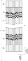
본 발명의 전형적인 실시형태에 있어서의 노광광의 중심위치의 조정방법에 대해서 이하 설명한다. 도 7은, 본 발명의 전형적인 실시형태에 있어서의 가변 슬 릿(중심위치 조정유닛)(8)의 구성을 나타내는 도면이다. 가변슬릿(8)은 개구로서의 슬릿을 규정하기 위한 부재로서 이동가능한 복수의 제1블레이드(30) 및 이동가능한 복수의 제2블레이드(31)를 포함한다. 제1블레이드(30)의 에지와 제2블레이드(31)의 에지 사이의 간격에 의해 슬릿의 주사축방향에 있어서의 길이(폭)가 결정된다.The method of adjusting the center position of the exposure light in the exemplary embodiment of the present invention will be described below. Fig. 7 is a diagram showing the configuration of the variable slit (center position adjusting unit) 8 in the exemplary embodiment of the present invention. The
가변슬릿(8)은 또, 복수의 제1리니어 액츄에이터(32) 및 복수의 제2리니어 액츄에이터(33)을 포함한다. 복수의 제1리니어 액츄에이터(32)는 주제어계(22)로부터의 지령에 따라 복수의 제1블레이드(30)를 주사축방향으로 구동한다. 복수의 제2리니어 액츄에이터(33)는 주제어계(22)로부터의 지령에 따라 복수의 제2블레이드 (31)를 주사축방향으로 구동한다.The
복수의 제1블레이드(30)는 제1가이드기구(34)에 의해 가이드 될 수 있다. 복수의 제2블레이드(31)는 제2가이드기구(35)에 의해 가이드 될 수 있다.The plurality of
도 8A 내지 도 8D는 가변슬릿의 조정과 노광광프로파일과의 관계를 나타내고 있다. 도 8A는 조정전의 가변슬릿(8) 상태를 예시하고, 도 8B는 도 8A에 도시된 상태에서의 가변슬릿(8)에 의해 형성되는 웨이퍼의 표면(투영광학계의 상면)에 있어서의 노광광 프로파일을 예시하고 있다. 도 8B는 조정전의 중심선과 목표중심선(기준선)이 예시적으로 도시하고 있다.8A to 8D show the relationship between the adjustment of the variable slit and the exposure light profile. Fig. 8A illustrates the state of the
도 8C는 노광광의 실제의 중심위치가 목표중심위치의 허용범위 내에 들어가도록 주제어계(22)로부터의 지령에 따라 복수의 제1액츄에이터(32)의 전부 또는일부 및 복수의 제2액츄에이터(33)의 전부 또는 일부를 동작시킨 상태를 예시하고 있다. 도 8D는 도 8C에 도시된 상태에서의 가변슬릿(8)에 의해 형성되는 웨이퍼의 표 면(투영광학계의 상면)에 있어서의 노광광 프로파일을 예시하고 있다.8C shows all or part of the plurality of
주제어계(22)에 의해, 중심위치를 조정하기 위한 블레이드(30) 및 (31)의 위치 D를, (1)식에 따라서 산출할 수 있다.By the
D = D_def + α × (P_1 - P_2) ... (1)D = D_def + α × (P_1-P_2) ... (1)
여기서, D_def는 조정전의 블레이드의 위치이고, α는 가변슬릿과 웨이퍼면 사이의 광학계의 배율이며, P_1은 목표노광광의 중심위치이고, P_2는 조정전의 노광광의 중심위치이다.Where D_def is the position of the blade before adjustment, α is the magnification of the optical system between the variable slit and the wafer surface, P_1 is the center position of the target exposure light, and P_2 is the center position of the exposure light before adjustment.
결상배율이 1의 경우는, 노광광의 중심위치의 어긋남을 보정하기 위해서, 가변슬릿(8)의 제1블레이드(30) 및 제2블레이드(31)를 노광광의 중심위치의 어긋남과 동일한 양만큼 구동하게 된다.When the imaging magnification is 1, in order to correct the misalignment of the center position of the exposure light, the
도 9는 노광광의 중심위치를 조정하는 순서를 나타내는 흐름도이다. 이 순서는 주제어계(22)에 의해 제어될 수 있다. 초기상태에서는, 가변슬릿(8)은 미리 정해진 상태로 배치되어 있다.9 is a flowchart showing a procedure of adjusting the center position of exposure light. This order can be controlled by the
스텝 101에서는, 주제어계(22)는 상높이 마다의 목표중심위치를 판독한다. 목표로 하는 중심위치(중심선 또는 기준선)는 감광제의 도포처리 등의 노광프로세스에 의존하기 때문에, 입력장치(24)를 통해 오퍼레이터에 의해 입력되는 데이터에 의거해서 결정될 수 있다. 예를 들면, EUV 리소그래피의 원호조명에 있어서, 조명영역이 원호형상인 경우는 중심선(기준선)은 원호형상의 곡선이다.In step 101, the
복수의 제1블레이드와 복수의 제2블레이드는 목표중심선에 의거해서 조정된다. 또, 중심위치는, 중심선에 의거하여 블레이드가이드기구를 설정함으로써, 블레 이드의 이동에 관계없이 상기 중심위치를 일정하게 유지해서, 초기부터 목표중심선 상에 있어도 된다. 예를 들면, 복수의 제1블레이드의 에지위치와 복수의 제2블레이드의 에지 위치 사이의 중간점에 광량중심위치가 있는 경우를 고려한다. 이 경우에 있어서, 제1블레이드의 이동량과 같은 이동량만큼 제2블레이드가 제1블레이드의 이동방향과 반대방향으로 이동한다고 하면, 상기 중심위치는 해당 중간점의 위치에서 잔류한다.The plurality of first blades and the plurality of second blades are adjusted based on the target center line. In addition, the center position may be on the target center line from the beginning by setting the blade guide mechanism based on the center line to keep the center position constant irrespective of the blade movement. For example, consider a case where there is a light quantity center position at an intermediate point between the edge positions of the plurality of first blades and the edge positions of the plurality of second blades. In this case, if the second blade moves in the direction opposite to the moving direction of the first blade by the moving amount equal to the moving amount of the first blade, the center position remains at the position of the intermediate point.
스텝 102에서, 주제어계(22)는, 투영광학계(15)의 상면에 있어서의 슬릿형상의 노광광의 광량을 상술한 방법에 따라 제2광전변환장치(검출기)(19)에 의해 검출함으로써, 상기 노광광의 상높이 마다의 중심위치를 구한다/계측한다.In step 102, the
스텝 103에서는, 주제어계(22)는, 스텝 103에서 얻어진 노광광의 중심위치의 적합성을 판정한다. 보다 구체적으로는, 주제어계(22)는, 예를 들면, 스텝 102에서 얻은 노광광의 중심위치와 스텝 101에서 취득한 목표중심위치를 비교해서, 이들의 차이가 허용범위 내에 들어가면 노광광의 중심위치는 "적합", 허용범위 밖에 있으면 "부적합"으로 판정한다. 주제어계(22)는 판정 결과가 "적합"인 경우에는, 처리를 스텝 106으로 진행하고, 판정 결과가 "부적합"인 경우에는, 처리를 스텝 102으로 복귀시킨다.In step 103, the
스텝 104에서는, 주제어계(22)는 (1) 식에 따라 복수의 제1블레이드(30)의 위치 및 복수의 제2블레이드(31)의 위치를 산출한다. 주제어계(22)는 그 산출 결과에 의거해서 복수의 제1리니어 액츄에이터(32) 및 복수의 제2리니어 액츄에이터(33)에 대한 구동지령치를 산출한다.In step 104, the
또한, (1) 식에 있어서, D_def는 스텝 102에서 중심위치를 계측했을 때의 블레이드(30) 및 (31)의 위치이고, P_1은 스텝 101에서 판독된 노광광의 목표중심 위치이며, P2는 스텝 102에서 계측된 노광광의 중심위치이다.In formula (1), D_def is the positions of the
복수의 제1블레이드(30) 및 복수의 제2블레이드(31)의 위치는, 노광광의 중심위치의 조정뿐만 아니라, 슬릿축방향의 조도불균일의 저감의 관점으로부터 결정되어도 된다.The positions of the plurality of
스텝 105에서는, 스텝 104에서 산출한 구동지령치를 복수의 제1리니어액츄에이터(32) 및 복수의 제2리니어 액츄에이터(33)로 보낸다. 이 동작에 의해, 복수의 제1블레이드(30)의 위치 및 복수의 제2블레이드(31)의 위치가 조정된다. 그 후, 다시, 스텝 102가 실행된다.In step 105, the drive command value calculated in step 104 is sent to the plurality of first
스텝 106에서는, 스텝 101에서 판독된 목표중심위치와 블레이드(30) 및 (31)의 구동량(리니어 액츄에이터(32) 및 (33)에 대한 구동지령치)을 보존한다. 웨이퍼의 노광순서의 실행에 있어서는, 이 때에 보존된 구동량에 의거해서 블레이드(30) 및 (31)가 구동된다.In step 106, the target center position and the drive amount (drive command values for the
스텝 107에서는, 주제어계(22)는 다른 조건에 대응하는 중심위치의 조정을 실시하는지의 여부를 판단한다. 중심위치조정을 실시하는 경우에는, 처리를 스텝 101로 복귀하고, 다른 조건에 대해서는, 스텝 101 내지 스텝 106의 처리를 반복한다. 이와 같이, 본 실시의 형태에서는, 복수의 조건(예를 들면, 복수의 조명조건 및 복수의 슬릿치수)의 각각에 대해서 블레이드(30) 및 (31)의 구동량(즉, 가변슬릿(8)의 설정)이 결정될 수 있다.In step 107, the
도 10은 웨이퍼를 노광하는 순서의 개략을 나타내는 순서도이다. 스텝 201에서는, 노광장치의 웨이퍼스테이지(17)에 웨이퍼가 반송된다. 이 반송에 수반해서, 주제어계(22)에 의한 제어하에서, 웨이퍼의 위치의 계측, 포커스면의 계측 등의 각종의 계측을 할 수 있다.10 is a flowchart showing an outline of a procedure of exposing a wafer. In step 201, the wafer is conveyed to the
스텝 202에서는, 주제어계(22)는 노광작업의 방법(recipe)에 포함되는, 예를 들면, 노광량, 노광광의 형상 등에 따라서, 스테이지(14) 및 (17)의 주사속도, 광원의 발진 주파수, 광원에 의해 방사되는 광의 목표에너지, 광원의 발광 펄스수, 가변슬릿(8)의 설정을 결정한다. 가변슬릿(8)의 설정에는, 복수의 제1블레이드(30) 및 복수의 제2블레이드(31)의 구동위치가 포함된다. 여기서, 가변슬릿(8)의 복수의 제1블레이드(30) 및 복수의 제2블레이드(31)의 구동위치는, 도 9에 나타내는 순서로 미리 보존된 정보에 의거해서 결정될 수 있다. 그러나, 노광작업의 방법에 포함되는 노광량, 노광광의 형상과 일치하는 조건에 있어서의 제1블레이드(30) 및 제2블레이드(31)의 구동위치가 미리 등록되지 않은 경우에는, 이들 조건하에서, 도 9의 스텝 101 내지 스텝 106의 순서를 실행해도 된다.In step 202, the
웨이퍼의 쇼트 영역내에 있어서의 노광량의 분포가 균일하지 않다고 가정한다. 주사축방향(Y방향)에 대해서는, 웨이퍼스테이지(17)의 주사속도와, 레이저의 발진 주파수 및 목표에너지를 조정하는 것에 의해 주사축방향에 있어서의 기판의 위치에 따라서 노광량을 변경한다. 슬릿축방향에 대해서는, 노광광의 슬릿축방향의 조도불균일을 저감하도록 제1블레이드(30)의 에지와 제2블레이드(31)의 에지 사이의 간격을 변경한다.It is assumed that the distribution of the exposure dose in the shot region of the wafer is not uniform. In the scanning axis direction (Y direction), the exposure amount is changed in accordance with the position of the substrate in the scanning axis direction by adjusting the scanning speed of the
제1블레이드(30) 및 제2블레이드(31)의 구동위치의 결정에 대해 보충설명을 한다. 주제어계(22)는 지정된 노광량에 의거해서, 최적인 노광광의 중심위치를 결정할 수 있다. 노광량과 이에 대응하는 최적인 노광광의 중심 위치와의 관계를 제공하는 미리 준비된 함수 또는 테이블을 주제어계(22)가 참조하여 이 결정을 행할 수 있다. 또, 상기 중심위치를 실현하기 위해서 노광광의 중심위치와 블레이드(30) 및 (31)의 구동량간의 관계를 나타내는 데이터를 도 9에 나타내는 순서의 반복에 의해 축적하고, 보간 처리함으로써, 임의의 중심위치를 실현하는 구동량을 결정해도 된다.The determination of the driving positions of the
스텝 203에서는, 주제어계(22)는 스텝 202에서 결정한 노광조건을 해당하는 제어계에 설정한다. 보다 구체적으로는, 주제어계(22)는 레이저(1)의 발진주파수, 목표에너지, 및 발광펄스수를 레이저제어계(23)에 설정하고, 스테이지(14) 및 (l7)의 주사속도를 스테이지 구동제어계(20)에서 설정하며, 가변슬릿(8)의 블레이드(30) 및(31)의 구동위치를 관련된 제어유닛(도시하지 않음)에 설정한다. 여기서, 가변 슬릿(8)에 있어서의 복수의 제1블레이드(30)와 복수의 제2블레이드(31)는 이 설정에 의거해서 노광의 개시전에 구동된다.In step 203, the
스텝 204에서는, 주제어계(22)는 웨이퍼를 노광하도록 각 제어계를 제어한다. 스테이지 구동제어계(20)는 설정된 조건에 따라 스테이지(14) 및 (17)를 구동하고, 레이저제어계(23)는 스테이지(14) 및 (17)의 이동과 동기시켜 레이저(1)의 발진을 제어한다.In step 204, the
스텝 205에서는, 주제어계(22)는 노광한 쇼트영역에 대한 노광결과를 판정한 다. 이 판정에는, 노광중의 광품위(예를 들면, 발진파장 및 선폭)의 판정과 쇼트영역에 대한 노광량의 판정이 포함될 수 있다.In step 205, the
광품위는, 예를 들면, 노광중에 모니터된 발진파장 및 선폭의, 이들의 설정치에 대한 절대오차나 펄스 마다의 이들의 불균일을 산출함으로써 판정된다. 각 산출치가 어느 쇼트영역의 노광에 있어서 에러 판정한계치를 초과한 경우에는, 이 노광은 에러로 판정된다. 또, 노광량은 도 3에 도시된 제1광전변환장치(6)에 의해 노광중에 모니터된 노광광량의 그 설정치에 대한 절대오차나 펄스 마다의 불균일을 산출함으로써 판정된다. 각 산출치가 어느 쇼트영역의 노광에 있어서 에러판정 한계치를 초과한 경우에는, 이 노광은 에러로 판정된다. 에러 판정이 이루어졌을 경우에는, 표시유닛(26) 등에 의해 에러정보가 오퍼레이터에게 제공된다.The light quality is determined, for example, by calculating the absolute error with respect to their set values or their non-uniformity per pulse of the oscillation wavelength and line width monitored during exposure. When each calculated value exceeds the error determination limit value in exposure of one shot area, this exposure is determined as an error. Incidentally, the exposure amount is determined by calculating the absolute error or nonuniformity per pulse with respect to the set value of the exposure light amount monitored during exposure by the first
스텝 206에서는, 주제어계(22)는 웨이퍼에 노광되어야 할 쇼트영역이 남아있는지의 여부를 판정한다. 노광되어야할 쇼트영역이 남아있는 경우에는, 주제어계 (22)는 처리를 스텝 202으로 복귀시키고 다음의 쇼트영역을 처리한다. 노광되어야할 쇼트영역이 남아있지 않는 경우에는, 주제어계(22)는 처리를 스텝 207으로 진행한다.In step 206, the
스텝 207에서는, 웨이퍼스테이지(17) 상의 노광된 웨이퍼가 웨이퍼보관케이스에 수납된다.In step 207, the exposed wafer on the
스텝 208에서는, 처리되어야할 웨이퍼가 남아있는지의 여부가 판정된다. 처리되어야할 웨이퍼가 남아있는 경우에는, 스텝 201 내지 스텝 207이 반복된다. 처리되어야 할 웨이퍼가 남아있지 않는 경우에는, 노광순서가 종료된다.In step 208, it is determined whether the wafer to be processed remains. If the wafer to be processed remains, steps 201 to 207 are repeated. If no wafer to be processed remains, the exposure procedure ends.
이상의 실시형태에서는, 노광광의 중심위치를 조정하기 위해 중심위치조정 닛으로서 가변슬릿(8)을 사용하는 예를 설명하고 있지만, 해당 중심위치 조정유닛은, 예를 들면, 마스킹블레이드(9), 또는 중성농도필터(도시하지 않음)이어도 된다. 중성농도필터는 광을 투과시키는 투광부와 광을 차광하는 차광부를 가진다. 투과부를 투과하는 광량이 위치에 따라서 변화한다.In the above embodiment, an example in which the
본 발명의 전형적인 실시형태에 의한 디바이스의 제조방법은 디바이스(예를 들면, 반도체디바이스 및 액정소자)의 제조에 적합하다. 이 방법은 상기 노광장치를 사용하여 감광제가 도포된 기판을 노광하는 공정, 및 상기 노광공정에서 노광된 기판을 현상하는 공정을 포함하고 있다. 상기 공정에 부가하여, 상기 디바이스의 제조방법은 기타 공지된 공정(예를 들면, 산화, 막형성, 증착, 도핑, 평탄화, 에칭, 레지스트제거, 다이싱, 본딩, 및 패키징공정)을 포함하고 있다.The device manufacturing method according to a typical embodiment of the present invention is suitable for the manufacture of devices (for example, semiconductor devices and liquid crystal elements). The method includes a step of exposing a substrate coated with a photosensitive agent using the exposure apparatus, and a step of developing a substrate exposed in the exposure step. In addition to the above process, the device manufacturing method includes other known processes (eg, oxidation, film formation, deposition, doping, planarization, etching, resist removal, dicing, bonding, and packaging processes). .
본 발명을 전형적인 실시예를 참조하면서 설명하였지만, 본 발명은 상기 개시된 전형적인 실시예로 한정되지 않는 것으로 이해되어야 한다. 이하 특허 청구범위는 이러한 모든 변경과 등가의 구성 및 기능을 망라하도록 최광의로 해석되어야 한다. While the invention has been described with reference to exemplary embodiments, it is to be understood that the invention is not limited to the exemplary embodiments disclosed above. The scope of the following claims is to be accorded the broadest interpretation so as to encompass all such modifications and equivalent constructions and functions.
도 1은 웨이퍼에 입사하는 노광광의 강도를 예시하는 도면;1 illustrates the intensity of exposure light incident on a wafer;
도 2A 및 도 2B는 노광광의 중심선의 만곡과 노광량과의 관계를 예시하는 도면;2A and 2B illustrate the relationship between the curvature of the centerline of exposure light and the exposure amount;
도 3은 본 발명의 바람직한 실시형태에 의한 주사노광장치의 개략구성을 나타내는 블럭도;3 is a block diagram showing a schematic configuration of a scanning exposure apparatus according to a preferred embodiment of the present invention;
도 4는 노광광의 중심 위치의 계측을 설명하기 위한 도면;4 is a diagram for explaining measurement of the center position of exposure light;
도 5는 노광광의 중심 위치의 계측을 설명하기 위한 그래프;5 is a graph for explaining measurement of the center position of exposure light;
도 6은 노광광의 중심 위치의 계측을 설명하기 위한 도면;6 is a diagram for explaining measurement of the center position of exposure light;
도 7은 가변 슬릿의 구성예를 나타내는 도면;7 shows an example of the configuration of a variable slit;
도 8A는 조정전의 가변 슬릿 상태를 예시하는 도면;8A illustrates a variable slit state before adjustment;
도 8B는 조정전의 가변 슬릿에 의해 형성되는 웨이퍼면(투영광학계의 상면)에 있어서의 노광광 프로파일을 예시하는 도면;8B is a diagram illustrating an exposure light profile on the wafer surface (upper surface of the projection optical system) formed by the variable slit before adjustment;
도 8C는 조정 후의 가변슬릿 상태를 예시하는 도면;8C illustrates the variable slit state after adjustment;
도 8D는 조정 후의 가변슬릿에 의해 형성되는 웨이퍼면(투영광학계의 상면)에 있어서의 노광광프로파일을 예시하는 도면;8D is a diagram illustrating an exposure light profile on the wafer surface (upper surface of the projection optical system) formed by the variable slit after adjustment;
도 9는 노광광의 중심위치를 조정하는 순서를 나타내는 흐름도;9 is a flowchart showing a procedure of adjusting the center position of exposure light;
도 10은 웨이퍼를 노광하는 순서의 개략을 나타내는 흐름도.10 is a flowchart showing an outline of a procedure of exposing a wafer.
[주요부분에 대한 도면부호의 설명][Description of reference numerals for the main parts]
1: 레이저(광원) 2: 빔정형광학계1: laser (light source) 2: beam shaping optical system
3: 옵티컬인티그레이터 4: 조리개 터릿3: optical integrator 4: aperture turret
5: 하프미러 6: 광전변환장치5: half mirror 6: photoelectric converter
7: 콘덴서렌즈 8: 가변슬릿7: Condenser Lens 8: Variable Slit
9: 마스킹 블레이드 10: 콘덴서렌즈9: masking blade 10: condenser lens
11: 미러 13: 레티클(원판)11: mirror 13: reticle (original)
14: 레티클스테이지 15: 투영광학계14: Reticle Stage 15: Projection Optical System
17: 웨이퍼스테이지 18: 웨이퍼17: wafer stage 18: wafer
19: 제2광전변환장치 20: 스테이지구동제어계19: second photoelectric conversion device 20: stage drive control system
21: 노광량 연산부 22: 주제어계21: exposure amount calculator 22: main controller
24: 입력장치 25: 기억유닛24: input device 25: storage unit
Claims (6)
Applications Claiming Priority (2)
| Application Number | Priority Date | Filing Date | Title |
|---|---|---|---|
| JP2008000804A JP2009164355A (en) | 2008-01-07 | 2008-01-07 | Scanning exposure apparatus and method of manufacturing device |
| JPJP-P-2008-000804 | 2008-01-07 |
Publications (1)
| Publication Number | Publication Date |
|---|---|
| KR20090076806A true KR20090076806A (en) | 2009-07-13 |
Family
ID=40844297
Family Applications (1)
| Application Number | Title | Priority Date | Filing Date |
|---|---|---|---|
| KR1020090000605A KR20090076806A (en) | 2008-01-07 | 2009-01-06 | Scanning exposure apparatus and device manufacturing method |
Country Status (4)
| Country | Link |
|---|---|
| US (1) | US8094289B2 (en) |
| JP (1) | JP2009164355A (en) |
| KR (1) | KR20090076806A (en) |
| TW (1) | TW200942979A (en) |
Families Citing this family (4)
| Publication number | Priority date | Publication date | Assignee | Title |
|---|---|---|---|---|
| JP6015930B2 (en) * | 2012-12-07 | 2016-10-26 | 株式会社ニコン | Exposure method, exposure apparatus, and device manufacturing method |
| US10139735B2 (en) | 2014-06-23 | 2018-11-27 | Asml Netherlands B.V. | Lithographic apparatus and method |
| JP6771997B2 (en) * | 2016-08-24 | 2020-10-21 | キヤノン株式会社 | Exposure equipment, exposure method, and article manufacturing method |
| JP6970548B2 (en) * | 2016-09-09 | 2021-11-24 | キヤノン株式会社 | Illumination optics, exposure equipment, and article manufacturing methods |
Family Cites Families (11)
| Publication number | Priority date | Publication date | Assignee | Title |
|---|---|---|---|---|
| US5854671A (en) * | 1993-05-28 | 1998-12-29 | Nikon Corporation | Scanning exposure method and apparatus therefor and a projection exposure apparatus and method which selectively chooses between static exposure and scanning exposure |
| JP3093528B2 (en) * | 1993-07-15 | 2000-10-03 | キヤノン株式会社 | Scanning exposure equipment |
| JPH0737776A (en) * | 1993-07-19 | 1995-02-07 | Nikon Corp | Scanning type aligner |
| JPH08250402A (en) * | 1995-03-15 | 1996-09-27 | Nikon Corp | Method and device for scanning exposure |
| KR100210569B1 (en) * | 1995-09-29 | 1999-07-15 | 미따라이 하지메 | Exposure method and exposure apparatus and method for manufacturing device using the same |
| JP2000232049A (en) * | 1999-02-09 | 2000-08-22 | Canon Inc | Aligner and device manufacturing method |
| JP2002110529A (en) * | 2000-10-03 | 2002-04-12 | Nikon Corp | Projection aligner and method of manufacturing micro device by using the same |
| JP4581639B2 (en) * | 2003-11-13 | 2010-11-17 | 株式会社ニコン | Variable slit apparatus, illumination apparatus, exposure apparatus, and device manufacturing method |
| US7119883B2 (en) * | 2004-10-13 | 2006-10-10 | Asml Holding N.V. | Correcting variations in the intensity of light within an illumination field without distorting the telecentricity of the light |
| US7375353B2 (en) * | 2005-09-13 | 2008-05-20 | Asml Netherlands B.V. | Lithographic apparatus and device manufacturing method |
| JP2009164356A (en) * | 2008-01-07 | 2009-07-23 | Canon Inc | Scanning exposure device and device manufacturing method |
-
2008
- 2008-01-07 JP JP2008000804A patent/JP2009164355A/en active Pending
- 2008-12-25 TW TW097150699A patent/TW200942979A/en unknown
-
2009
- 2009-01-06 US US12/349,439 patent/US8094289B2/en not_active Expired - Fee Related
- 2009-01-06 KR KR1020090000605A patent/KR20090076806A/en active IP Right Grant
Also Published As
| Publication number | Publication date |
|---|---|
| US20090174875A1 (en) | 2009-07-09 |
| US8094289B2 (en) | 2012-01-10 |
| JP2009164355A (en) | 2009-07-23 |
| TW200942979A (en) | 2009-10-16 |
Similar Documents
| Publication | Publication Date | Title |
|---|---|---|
| US6730925B1 (en) | Method and apparatus for projection exposure and device manufacturing method | |
| US5677754A (en) | Scanning exposure apparatus | |
| JPH0774092A (en) | Aligner and manufacture of device using the same | |
| KR102002666B1 (en) | Exposure apparatus, exposure method, and device manufacturing method | |
| JP3913079B2 (en) | Surface position detection apparatus and method, exposure apparatus, and device manufacturing method using the exposure apparatus | |
| US7612868B2 (en) | Exposure apparatus and method of manufacturing device | |
| JP6267530B2 (en) | Exposure apparatus and article manufacturing method | |
| KR20090076806A (en) | Scanning exposure apparatus and device manufacturing method | |
| KR20090028410A (en) | Exposure system and method of manufacturing a semiconductor device | |
| JPH0737774A (en) | Scanning aligner | |
| US10488764B2 (en) | Lithography apparatus, lithography method, and method of manufacturing article | |
| US20070285646A1 (en) | Exposure apparatus | |
| JPH11354425A (en) | Scanning projection aligner and manufacture of device using the same | |
| KR20180138544A (en) | Exposure apparatus, and method of manufacturing article | |
| US20100103393A1 (en) | Scanning exposure apparatus and device manufacturing method | |
| JP2004342900A (en) | Aligner, and reticle profile measurement device and method | |
| US8416389B2 (en) | Exposure apparatus and method of manufacturing device | |
| KR101660090B1 (en) | Exposure method, exposure apparatus, and method of manufacturing device | |
| KR20100006128A (en) | Scanning exposure apparatus and method of manufacturing device | |
| US20110123934A1 (en) | Scanning exposure apparatus | |
| US9329498B2 (en) | Exposure apparatus and method of manufacturing article | |
| US5757838A (en) | Output control method for excimer laser | |
| JP2016218407A (en) | Exposure apparatus, exposure method and producing method of product | |
| KR20070033136A (en) | Method for adjusting focal length of an exposure apparatus | |
| CN111356955A (en) | Exposure apparatus and article manufacturing method |
Legal Events
| Date | Code | Title | Description |
|---|---|---|---|
| A201 | Request for examination | ||
| E701 | Decision to grant or registration of patent right | ||
| NORF | Unpaid initial registration fee |