KR20090058527A - Led backlight - Google Patents
Led backlight Download PDFInfo
- Publication number
- KR20090058527A KR20090058527A KR1020097005700A KR20097005700A KR20090058527A KR 20090058527 A KR20090058527 A KR 20090058527A KR 1020097005700 A KR1020097005700 A KR 1020097005700A KR 20097005700 A KR20097005700 A KR 20097005700A KR 20090058527 A KR20090058527 A KR 20090058527A
- Authority
- KR
- South Korea
- Prior art keywords
- film
- optical film
- reflective
- led
- reflective surface
- Prior art date
Links
Images


Classifications
-
- H—ELECTRICITY
- H01—ELECTRIC ELEMENTS
- H01L—SEMICONDUCTOR DEVICES NOT COVERED BY CLASS H10
- H01L33/00—Semiconductor devices with at least one potential-jump barrier or surface barrier specially adapted for light emission; Processes or apparatus specially adapted for the manufacture or treatment thereof or of parts thereof; Details thereof
-
- G—PHYSICS
- G02—OPTICS
- G02F—OPTICAL DEVICES OR ARRANGEMENTS FOR THE CONTROL OF LIGHT BY MODIFICATION OF THE OPTICAL PROPERTIES OF THE MEDIA OF THE ELEMENTS INVOLVED THEREIN; NON-LINEAR OPTICS; FREQUENCY-CHANGING OF LIGHT; OPTICAL LOGIC ELEMENTS; OPTICAL ANALOGUE/DIGITAL CONVERTERS
- G02F1/00—Devices or arrangements for the control of the intensity, colour, phase, polarisation or direction of light arriving from an independent light source, e.g. switching, gating or modulating; Non-linear optics
- G02F1/01—Devices or arrangements for the control of the intensity, colour, phase, polarisation or direction of light arriving from an independent light source, e.g. switching, gating or modulating; Non-linear optics for the control of the intensity, phase, polarisation or colour
- G02F1/13—Devices or arrangements for the control of the intensity, colour, phase, polarisation or direction of light arriving from an independent light source, e.g. switching, gating or modulating; Non-linear optics for the control of the intensity, phase, polarisation or colour based on liquid crystals, e.g. single liquid crystal display cells
- G02F1/133—Constructional arrangements; Operation of liquid crystal cells; Circuit arrangements
- G02F1/1333—Constructional arrangements; Manufacturing methods
- G02F1/1335—Structural association of cells with optical devices, e.g. polarisers or reflectors
- G02F1/1336—Illuminating devices
- G02F1/133602—Direct backlight
- G02F1/133603—Direct backlight with LEDs
-
- F—MECHANICAL ENGINEERING; LIGHTING; HEATING; WEAPONS; BLASTING
- F21—LIGHTING
- F21S—NON-PORTABLE LIGHTING DEVICES; SYSTEMS THEREOF; VEHICLE LIGHTING DEVICES SPECIALLY ADAPTED FOR VEHICLE EXTERIORS
- F21S8/00—Lighting devices intended for fixed installation
-
- G—PHYSICS
- G02—OPTICS
- G02F—OPTICAL DEVICES OR ARRANGEMENTS FOR THE CONTROL OF LIGHT BY MODIFICATION OF THE OPTICAL PROPERTIES OF THE MEDIA OF THE ELEMENTS INVOLVED THEREIN; NON-LINEAR OPTICS; FREQUENCY-CHANGING OF LIGHT; OPTICAL LOGIC ELEMENTS; OPTICAL ANALOGUE/DIGITAL CONVERTERS
- G02F1/00—Devices or arrangements for the control of the intensity, colour, phase, polarisation or direction of light arriving from an independent light source, e.g. switching, gating or modulating; Non-linear optics
- G02F1/01—Devices or arrangements for the control of the intensity, colour, phase, polarisation or direction of light arriving from an independent light source, e.g. switching, gating or modulating; Non-linear optics for the control of the intensity, phase, polarisation or colour
- G02F1/13—Devices or arrangements for the control of the intensity, colour, phase, polarisation or direction of light arriving from an independent light source, e.g. switching, gating or modulating; Non-linear optics for the control of the intensity, phase, polarisation or colour based on liquid crystals, e.g. single liquid crystal display cells
- G02F1/133—Constructional arrangements; Operation of liquid crystal cells; Circuit arrangements
- G02F1/1333—Constructional arrangements; Manufacturing methods
- G02F1/1335—Structural association of cells with optical devices, e.g. polarisers or reflectors
- G02F1/1336—Illuminating devices
- G02F1/133602—Direct backlight
- G02F1/133605—Direct backlight including specially adapted reflectors
-
- G—PHYSICS
- G02—OPTICS
- G02F—OPTICAL DEVICES OR ARRANGEMENTS FOR THE CONTROL OF LIGHT BY MODIFICATION OF THE OPTICAL PROPERTIES OF THE MEDIA OF THE ELEMENTS INVOLVED THEREIN; NON-LINEAR OPTICS; FREQUENCY-CHANGING OF LIGHT; OPTICAL LOGIC ELEMENTS; OPTICAL ANALOGUE/DIGITAL CONVERTERS
- G02F1/00—Devices or arrangements for the control of the intensity, colour, phase, polarisation or direction of light arriving from an independent light source, e.g. switching, gating or modulating; Non-linear optics
- G02F1/01—Devices or arrangements for the control of the intensity, colour, phase, polarisation or direction of light arriving from an independent light source, e.g. switching, gating or modulating; Non-linear optics for the control of the intensity, phase, polarisation or colour
- G02F1/13—Devices or arrangements for the control of the intensity, colour, phase, polarisation or direction of light arriving from an independent light source, e.g. switching, gating or modulating; Non-linear optics for the control of the intensity, phase, polarisation or colour based on liquid crystals, e.g. single liquid crystal display cells
- G02F1/133—Constructional arrangements; Operation of liquid crystal cells; Circuit arrangements
- G02F1/1333—Constructional arrangements; Manufacturing methods
- G02F1/1335—Structural association of cells with optical devices, e.g. polarisers or reflectors
- G02F1/1336—Illuminating devices
- G02F1/133602—Direct backlight
- G02F1/133611—Direct backlight including means for improving the brightness uniformity
Abstract
Description
본 발명은 대체로 LED 백라이트 어셈블리에 관한 것이다.The present invention relates generally to an LED backlight assembly.
발광 다이오드(LED)는 다양한 응용예에 대한 광원으로서 사용된다. 일부 LED 광원의 응용예는 상업용 그래픽 표시 장치 및 기타 조명 표시 장치를 포함한다. LED 발광 패턴은 전방으로 유도되는 좁은 빔에서 넓은 원뿔형까지 다양할 수 있다. 측면 발광 LED도 또한 일부 응용예에 사용된다.Light emitting diodes (LEDs) are used as light sources for various applications. Applications of some LED light sources include commercial graphics displays and other lighting displays. LED light emitting patterns can vary from narrow beams leading forward to wide cones. Side emitting LEDs are also used in some applications.
이들 응용예에서, LED는 통상 백라이트의 배면 또는 측면 상에 배치된다. LED가 백라이트의 배면 상에 배치되어 있는 경우, LED 광원에 의해 야기된 휘점(bright spot)이 백라이트 출력에서 보일 수 있고, 그에 따라 발광이 균일하지 못한 간판 박스(sign box) 또는 표시 장치를 가져올 수 있다.In these applications, LEDs are typically disposed on the back or side of the backlight. If the LED is placed on the back of the backlight, bright spots caused by the LED light source may be visible at the backlight output, resulting in a sign box or display device with uneven light emission. have.
이들 응용예에서, 백라이트에 확산기를 배치하면 휘점을 최소화할 수 있다. 이들 확산기는 백라이트 주변의 광을 반사하여 방출된 광을 균질화할 수 있지만, 모든 반사는 광의 손실을 야기할 수 있고, 확산기 또한 투과된 광을 감소시킬 수 있다.In these applications, placing the diffuser in the backlight can minimize the bright spot. These diffusers can reflect light around the backlight to homogenize the emitted light, but all reflections can cause loss of light, and the diffuser can also reduce the transmitted light.
간판 박스 또는 표시 장치에서 감지되는 LED 휘점을 감소시키는 다른 방법은 간판 박스 또는 표시 장치를 더 깊게 만드는 것이다. 그러나, 이 또한 광원으로부터 표시 장치 또는 간판면(발광 표면)까지의 간격을 증가시킴으로 인해 휘도 손실 을 야기할 수 있다. 또한 추가 재료에 대한 필요로 인해 상당한 비용 증가를 초래할 수도 있다.Another way to reduce the LED bright spots detected in the signage box or display device is to make the signage box or display device deeper. However, this may also cause loss of brightness due to increasing the distance from the light source to the display device or signboard surface (light emitting surface). The need for additional materials may also result in significant cost increases.
일 태양에서, 본 발명은 복수의 내부 표면을 갖는 하우징을 포함하는 LED 백라이트 어셈블리를 제공한다. 내부 표면 중 적어도 하나는 발광 표면이고, 대향 표면은 반사 표면이다. 발광 표면과 반사 표면 사이에 광학 필름이 배치된다. 광학 필름은 확산 필름, 반사 편광 필름, 다층 광학 필름, 및 구조화된 표면 필름 중 적어도 하나를 포함한다. 전기적으로 연결된 LED 어레이가 광학 필름 상에 배치된다. LED 어레이에서 적어도 하나의 LED는 반사 표면을 향하는 조명 필드(illumination field)를 갖는다.In one aspect, the invention provides an LED backlight assembly comprising a housing having a plurality of interior surfaces. At least one of the inner surfaces is a light emitting surface and the opposing surface is a reflective surface. An optical film is disposed between the light emitting surface and the reflective surface. The optical film includes at least one of a diffusing film, a reflective polarizing film, a multilayer optical film, and a structured surface film. An electrically connected LED array is disposed on the optical film. At least one LED in the LED array has an illumination field facing the reflective surface.
다른 태양에서, 본 발명은 복수의 내부 표면을 갖는 하우징을 포함하는 LED 백라이트 어셈블리를 제공한다. 내부 표면 중 적어도 하나는 발광 표면이고, 대향 표면은 반사 표면이다. 발광 표면과 반사 표면 사이에 광학 필름이 배치된다. 광학 필름은 확산 필름, 반사 편광 필름, 다층 광학 필름, 및 구조화된 표면 필름 중 적어도 하나를 포함한다. 광학 필름은 비평면이고, 광학 필름의 일부는 반사 표면 상에 배치된다. 전기적으로 연결된 LED 어레이가 광학 필름 상에 배치된다. LED 어레이에서 적어도 하나의 LED는 반사 표면을 향하는 조명 필드를 갖는다.In another aspect, the present invention provides an LED backlight assembly comprising a housing having a plurality of interior surfaces. At least one of the inner surfaces is a light emitting surface and the opposing surface is a reflective surface. An optical film is disposed between the light emitting surface and the reflective surface. The optical film includes at least one of a diffusing film, a reflective polarizing film, a multilayer optical film, and a structured surface film. The optical film is non-planar and a portion of the optical film is disposed on the reflective surface. An electrically connected LED array is disposed on the optical film. At least one LED in the LED array has an illumination field facing the reflective surface.
다른 태양에서, 본 발명은 LED 백라이트 어셈블리의 제조 방법을 제공한다. 본 방법은, 적어도 하나가 발광 표면이고 대향 표면은 반사 표면인 복수의 내부 표면을 갖는 하우징을 제공하는 단계, 확산 필름, 반사 편광 필름, 다층 광학 필름 및 구조화된 표면 필름 중 적어도 하나를 포함하는 광학 필름 상에 LED 어레이 및 도전체를 배치하는 단계, 및 LED 어레이에서 적어도 하나의 LED가 반사 표면을 향하는 조명 필드를 갖도록 발광 표면과 반사 표면 사이에 광학 필름을 배치하는 단계를 포함한다.In another aspect, the present invention provides a method of manufacturing an LED backlight assembly. The method comprises providing a housing having a plurality of interior surfaces, at least one of which is a light emitting surface and an opposing surface, wherein the optical comprises at least one of a diffusing film, a reflective polarizing film, a multilayer optical film and a structured surface film. Disposing an LED array and conductors on the film, and disposing an optical film between the light emitting surface and the reflective surface such that at least one LED in the LED array has an illumination field facing the reflective surface.
본 발명에 따른 LED 백라이트 어셈블리의 이들 및 다른 태양이 도면과 함께 후속하는 상세한 설명으로부터 당업자에게 보다 용이하게 명백하게 될 것이다.These and other aspects of the LED backlight assembly according to the present invention will become more readily apparent to those skilled in the art from the following detailed description in conjunction with the drawings.
본 발명이 속하는 기술 분야의 통상의 기술을 가진 자가 본 발명의 제조 및 사용 방법을 보다 쉽게 이해할 수 있도록, 본 발명의 예시적인 실시예를 다음의 도면을 참조하여 이하에서 상세히 설명하기로 한다.Exemplary embodiments of the present invention will be described in detail below with reference to the accompanying drawings so that those skilled in the art to which the present invention pertains can easily understand the methods of making and using the present invention.
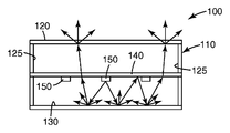
도 1은 하나의 예시적인 LED 백라이트 어셈블리의 개략 단면도이다.1 is a schematic cross-sectional view of one exemplary LED backlight assembly.
도 2는 예시적인 광학 필름 및 부속된 LED의 개략 부분 단면도이다.2 is a schematic partial cross-sectional view of an exemplary optical film and attached LED.
도 3은 다른 예시적인 광학 필름 및 부속된 LED의 개략 부분 단면도이다.3 is a schematic partial cross-sectional view of another exemplary optical film and attached LED.
도 4는 추가의 예시적인 광학 필름 및 부속된 LED의 개략 부분 단면도이다.4 is a schematic partial cross-sectional view of a further exemplary optical film and attached LED.
도 5는 도 1의 LED 백라이트에 유용한 예시적인 광학 필름 구성의 개략 사시도이다.5 is a schematic perspective view of an exemplary optical film configuration useful for the LED backlight of FIG. 1.
도 6은 하나의 예시적인 LED 백라이트 어셈블리의 개략 부분 단면도이다.6 is a schematic partial cross-sectional view of one exemplary LED backlight assembly.
본 발명은 LED 백라이트에 대해 설명한다. 이들 LED 백라이트에서의 LED는 LED가 백라이트의 표시 장치 표면 밖으로 직접 광을 방출하지 않도록 위치된다. 이 방식으로, LED는 직접 보이지 않고, LED에 의해 방출된 광은 광이 LED 백라이트의 표시 장치 표면 밖으로 방출되기 전에 LED 백라이트 내의 반사 표면에서의 적어도 한 번의 반사에 의해 확산될 수 있다. 따라서, 본 발명은 LED에 의해 야기되는 휘점이 표시 장치 표면에서 보이지 않도록 표시 장치 표면의 균일한 조명을 제공하는 LED 백라이트로 조명된 표시 장치 표면에 대해 설명한다.The present invention describes an LED backlight. LEDs in these LED backlights are positioned such that the LEDs do not emit light directly outside the display surface of the backlight. In this way, the LED is not directly visible and the light emitted by the LED can be diffused by at least one reflection at the reflective surface in the LED backlight before the light is emitted out of the display surface of the LED backlight. Accordingly, the present invention describes a display device surface illuminated with an LED backlight that provides uniform illumination of the display device surface such that bright spots caused by the LED are not visible at the display device surface.
따라서, 본 발명은 대체로 LED 백라이트에 관한 것으로, 특히 LED 백라이트 내의 광학 필름 상에 배치되는 LED 어레이를 포함하는 LED 백라이트에 관한 것이다. LED는 방출된 광이 광학 필름으로부터 멀어지는 방향으로 향하도록 배면을 향할 수 있고, 광학 필름은 표시 장치로부터 방출된 광이 향상되도록 백라이트의 반사 표면으로부터 돌아오는 LED 방출 광을 관리한다. 또한, 광학 필름은 배면을 향하는 LED의 위치 및 광학 필름 상에 배치된 관련 전기 트레이스를 숨기는 것을 돕도록 이러한 필름을 통과하는 광을 방향 전환시키는 것을 도울 수 있다. 본 발명은 이로 한정되지 않으며, 본 발명의 다양한 태양에 대한 이해는 본 명세서에 제공된 예들의 논의를 통해 얻을 수 있다. Accordingly, the present invention relates generally to LED backlights, and more particularly to LED backlights comprising an LED array disposed on an optical film in the LED backlight. The LED may face the back so that the emitted light is directed away from the optical film, and the optical film manages the LED emitting light returning from the reflective surface of the backlight to enhance the light emitted from the display device. The optical film can also help redirect the light passing through the film to help hide the position of the LED facing the back and the associated electrical traces disposed on the optical film. The invention is not so limited, and an understanding of various aspects of the invention can be obtained through a discussion of the examples provided herein.
하기의 설명은 도면을 참조하면서 파악되어야 하며, 이들 도면에서 여러 도면 중 유사한 요소들은 유사한 방식으로 번호가 매겨져 있다. 반드시 척도에 맞게 도시될 필요는 없는 도면이 소정의 예시적인 실시 형태들을 도시하고 있으며 본 발명의 범주를 제한하고자 하는 것은 아니다. 구성, 치수 및 재료의 예들이 다양한 요소들에 대하여 도시되었으나, 당업자는 제공된 예들의 대부분은 활용될 수 있는 적당한 대안을 가짐을 알게 될 것이다.The following description should be read with reference to the drawings, in which like elements in the various figures are numbered in a similar manner. The drawings, which are not necessarily drawn to scale, illustrate certain exemplary embodiments and are not intended to limit the scope of the invention. Although examples of configurations, dimensions, and materials have been shown for various elements, those skilled in the art will recognize that many of the examples provided have suitable alternatives that may be utilized.
달리 지시되지 않는 한, 본 명세서 및 청구의 범위에 사용된 특징부 크기, 양 및 물리적 특성을 표현하는 모든 숫자는 모든 경우에 용어 "약"에 의해 수식되는 것으로 이해되어야 한다. 따라서, 반대로 지시되지 않는 한, 이어지는 명세서 및 첨부된 청구의 범위에 기술된 수치적 파라미터는 본 명세서에 개시된 교시를 이용하는 당업자가 얻고자 하는 원하는 특성에 따라 변할 수 있는 근사치이다.Unless otherwise indicated, all numbers expressing feature sizes, quantities, and physical properties used in the specification and claims are to be understood as being modified in all instances by the term "about." Accordingly, unless indicated to the contrary, the numerical parameters set forth in the following specification and appended claims are approximations that may vary depending upon the desired properties sought by those skilled in the art using the teachings disclosed herein.
종점(endpoint)들에 의한 수치 범위의 설명은 범위 내에 포함되는 모든 숫자를 포함하며(예를 들어, 1 내지 5는 1, 1.5, 2, 2.75, 3, 3.80, 4 및 5를 포함함), 범위 내의 임의의 범위를 포함한다.The description of the numerical range by endpoints includes all numbers falling within the range (eg 1 to 5 includes 1, 1.5, 2, 2.75, 3, 3.80, 4 and 5), It includes any range within the range.
본 명세서 및 첨부된 청구의 범위에 사용될 때, 단수형은 그 내용이 명백하게 달리 지시하지 않으면 복수의 지시 대상을 갖는 실시예를 포함한다. 본 명세서 및 첨부된 청구의 범위에 사용될 때, "또는"이라는 용어는 그 내용이 명백하게 달리 지시하지 않는 한 "및/또는"을 포함하는 의미로 일반적으로 이용된다.As used in this specification and the appended claims, the singular forms "a", "an", and "the" include plural referents unless the content clearly dictates otherwise. As used in this specification and the appended claims, the term "or" is generally employed in its sense including "and / or" unless the content clearly dictates otherwise.
도 1은 하나의 예시적인 LED 백라이트(100)의 개략 단면도이다. 도 5는 도 1의 LED 백라이트(100)에 유용한 예시적인 광학 필름(140)의 개략 사시도이다. 백라이트(100)는 복수의 내부 표면을 갖는 하우징(110)을 포함한다. 내부 표면 중 적어도 하나는 발광 표면(120)이고, 대향 표면은 반사 표면(130)이다. 도시된 백라이트(100)는 대향하는 측면들(125)을 포함한다. 백라이트는 또한 도면의 평면에 실질적으로 평행한 대향 측면들을 포함할 수 있다. 대향하는 측면들(125), 발광 표면(120), 및 반사 표면(130)은 다 함께 라이트 박스(light box) 또는 수납형 백라이트를 형성한다.1 is a schematic cross-sectional view of one
발광 표면(120)은 원하는 방출 광의 투과를 허용하는 임의의 재료로 형성될 수 있다. 일부 실시예에서, 발광 표면(120)은 확산 투광 표면 또는 반투명 표면이다.The
반사 표면(130)은 바람직하게는 향상된 백라이트 효율을 위해 고반사성을 갖는다. 예를 들어, 반사 표면(130)은 LED 어레이(150)에 의해 방출된 가시광에 대하여 적어도 90%, 95%, 98%, 99% 또는 그 이상의 평균 반사율을 가질 수 있다. 반사 표면(130)은 공간적으로 균일하든지 패터닝되든지 어느 것이든 간에 현저한 경면 반사형, 확산형, 또는 조합된 경면 반사형/확산형 반사기일 수 있다. 몇몇 경우에, 반사 표면(130)은 고반사율의 코팅을 갖는 강성의 금속 기판 또는 지지 기판에 적층된 고반사율의 필름으로 제조될 수 있다. 적합한 고반사율 재료로는 쓰리엠 컴퍼니(3M Company)로부터 입수가능한 비퀴티(Vikuiti™) 인핸스드 스펙큘러 리플렉터(Enhanced Specular Reflector, ESR) 다층 광학 필름; 10 마이크로미터(0.4 밀) 두께의 아이소옥틸아크릴레이트 아크릴산 감압 접착제를 사용하여 비퀴티 ESR 필름에 황산 바륨이 함유된 폴리에틸렌 테레프탈레이트 필름(50.8 마이크로미터(2 밀) 두께)을 적층하여 제조된 필름으로서, 결과로서의 적층체 필름이 본 명세서에서 "EDR II" 필름으로 불리는 필름; 쓰리엠 컴퍼니로부터 입수가능한 3M™ 라이트 인핸스먼트 필름(Light Enhancement Film); 토레이 인더스트리즈, 인크.(Toray Industries, Inc.)로부터 입수가능한 E-60 시리즈 루미러(Lumirror™) 폴리에스테르 필름; 더블유. 엘. 고어 앤 어소시에이츠, 인크.(W. L. Gore & Associates, Inc.)로부터 입수가능한 것과 같은 다공성 폴리테트라플루오로에틸렌(PTFE) 필름; 랩스피어, 인크.(Labspher, Inc.)로부터 입수가능한 스펙트랄론(Spectralon™) 반사 재료; 알라노드 알루미늄-페레트룽 게엠베하 운트 코.(Alanod Aluminium-Veredlung GmbH & Co.)로부터 입수가능한 미로(Miro™) 양극산화 알루미늄 필름(미로 2 필름을 포함); 후루카와 일렉트릭 컴퍼니, 엘티디.(Furukawa Electric Co, Ltd.)로부터의 MCPET 고반사율 발포 시트(foamed sheeting); 및 미츠이 케미칼즈, 인크.(Mitsui Chemicals, Inc.)로부터 입수가능한 화이트 레프스타 필름 및 MT 필름(White Refstar™ films and MT films)을 포함한다. 일부 실시예에서, 반사 표면(130)은 확산 반사 페인트를 포함할 수 있다.
반사 표면(130)은 실질적으로 평평하고 매끄러울 수 있거나, 또는 광 산란 또는 혼합을 향상시키기 위해 그에 결합된 구조화된 표면을 가질 수 있다. 이러한 구조화된 표면은 (a) 반사 표면 상에, 또는 (b) 반사 표면(130)에 도포된 투명 코팅 상에 부여될 수 있다. 전자의 경우에, 구조화된 표면이 이미 형성된 기판에 고반사 필름이 적층될 수 있거나, 또는 고반사 필름이 (쓰리엠 컴퍼니로부터 입수가능한 비퀴티 듀라블 인핸스드 스펙큘러 리플렉터-메탈(Durable Enhanced Specular Reflector-Metal, DESR-M) 반사기와 같이 얇은 금속 시트와 같은) 평평한 기판에 적층되고 스탬핑(stamping) 작업과 같은 것으로써 구조화된 표면을 형성하는 것이 이어질 수 있다. 후자의 경우에, 구조화된 표면을 갖는 투명 필름이 평평한 반사 표면에 적층될 수 있거나, 또는 투명 필름이 반사기에 도포되고 이어서 이후 구조화된 표면이 투명 필름의 상부에 부여될 수 있다.
광학 필름(140)은 발광 표면(120)과 반사 표면(130) 사이에 배치된다. 광학 필름(140)은 임의의 적합한 광학 필름 또는 층, 예를 들어 확산 필름, 반사 편광 필름, 다층 광학 필름, 또는 구조화된 표면 필름 중 적어도 하나를 포함할 수 있다. LED 어레이(150)는 광학 필름(140) 상에 배치된다. LED 어레이(150)는, 예를 들어 기계적 체결, 솔더링, 또는 접착제로 광학 필름(140)에 LED(150)를 접착시키는 것과 같은 임의의 유용한 기술에 의해 광학 필름(140)에 장착될 수 있다.The
LED 어레이(150)를 형성하는 LED는 LED가 원하는 바와 같이 직렬이나 병렬 방식으로 또는 직렬과 병렬의 조합으로 작동할 수 있도록 전기적으로 연결된다. LED 어레이(150)에서 적어도 하나의 LED는 반사 표면(130)을 향하는 조명 필드를 갖는다. 일부 실시예에서, LED 어레이(150)에서 각각의 LED는 반사 표면(130)을 향하는 조명 필드를 갖는다.The LEDs forming the
"발광 다이오드" 또는 "LED"는 가시광선이든, 자외선이든 또는 적외선이든지 간에, 광을 방출하는 다이오드를 가리킨다. 이는, 종래의 유형이든지 초복사성(super radiant) 유형이든지 간에, 그리고 전면 발광(forward-emitting) 유형이든지 측면 발광(side-emitting) 유형이든지 간에, 비결집성(incoherent) LED 다이 또는 "LED"로서 시판되는 내장 또는 봉지된 반도전체 소자를 포함하는데, 이들 중 후자는 종종 표시 장치 응용예에 유리하다. LED가 자외선광과 같은 비가시광을 방출한다면, 그리고 가시광을 방출하는 몇몇 경우에, LED는 단파장 광을 장파장 가시광으로 변환하기 위해 유기 또는 무기 형광체를 포함하도록 패키징될 수 있고(또는 원격 배치된 형광체를 조명할 수도 있음), 몇몇 경우에 백색광을 방출하는 장치가 얻어질 수 있다. "LED 다이"는 가장 기본적인 형태, 즉 반도전체 가공 절차에 의 해 제조된 개별 구성요소 또는 칩(chip) 형태의 LED이다. 예를 들어, LED 다이는 하나 이상의 III족 원소와 하나 이상의 V족 원소의 조합(III-V족 반도전체)으로 보통 형성된다. 적합한 III-V족 반도전체 재료의 예는 질화갈륨과 같은 질화물, 및 인듐 갈륨 포스파이드와 같은 인화물(phosphide)을 포함한다. 주기율표의 다른 족의 무기 재료일 수 있는 다른 유형의 III-V족 재료가 또한 사용될 수 있다. 이 구성요소 또는 칩은 소자에 에너지를 공급하기 위한 전력의 인가에 적합한 전기 접촉부를 포함할 수 있다. 구성요소 또는 칩의 개개의 층 및 다른 기능 요소는 전형적으로 웨이퍼 규모로 형성되고, 완성된 웨이퍼는 이어서 개별적인 단품(piece part)으로 절단되어 다수의 LED 다이가 얻어질 수 있다. LED 다이는 표면 실장, 칩 온 보드(chip-on-board), 플립칩 또는 기타 공지된 실장 구성용으로 구성될 수 있다. 일부 패키징된 LED는 LED 다이 및 관련 반사기 컵(reflector cup) 위에 형성되는 중합체 봉지재를 형성함으로써 제조된다."Light emitting diode" or "LED" refers to a diode that emits light, whether visible light, ultraviolet light or infrared light. It is marketed as an "incoherent" LED die or "LED", whether conventional or super radiant type, and whether it is a forward-emitting type or a side-emitting type. Embedded or encapsulated semiconducting elements, the latter of which are often advantageous for display device applications. If the LED emits invisible light, such as ultraviolet light, and in some cases that emits visible light, the LED can be packaged to include organic or inorganic phosphors to convert short wavelength light into long wavelength visible light (or remotely disposed phosphors). Lighting), in some cases a device can be obtained which emits white light. An "LED die" is an LED in its most basic form, ie in the form of discrete components or chips manufactured by semiconductor manufacturing processes. For example, an LED die is usually formed of a combination of one or more Group III elements and one or more Group V elements (Group III-V semiconductors). Examples of suitable III-V semiconducting materials include nitrides such as gallium nitride, and phosphides such as indium gallium phosphide. Other types of group III-V materials may also be used, which may be inorganic materials of other groups of the periodic table. This component or chip may include electrical contacts suitable for application of power to energize the device. Individual layers of components or chips and other functional elements are typically formed on a wafer scale, and the finished wafer can then be cut into individual piece parts to obtain multiple LED dies. The LED die may be configured for surface mount, chip-on-board, flip chip or other known mounting configurations. Some packaged LEDs are manufactured by forming a polymer encapsulant that is formed over the LED die and associated reflector cups.
도 5에 도시된 바와 같이, LED 어레이(150)에서 LED는 전기 도전체(160)를 통하여 전기적으로 연결된다. 전기 도전체(160)는 공급 도전체 및 접지 도전체를 포함한다. 전기 도전체(160)는 임의의 유용한 구성으로 배열될 수 있으며 도 5에 도시된 구성으로 한정되지 않음을 이해하여야 한다. 전기 도전체(160)는 임의의 적합한 기술을 사용하여 광학 필름(140) 상에 또는 그 내에 배치될 수 있다.As shown in FIG. 5, the LEDs in the
도전성 잉크(예를 들어, 은 잉크, 구리 잉크, 니켈계 잉크)가 전기 도전체(160)를 형성할 수 있다. 도전성 잉크는 광학 필름(140) 상에 실크 스크린되거나 인쇄될 수 있다. 광학 필름(140) 상에 도전체(160)를 형성하는 다른 방법으로 는, 광학 필름(140)에 구리 호일을 적층하고, 포토레지스트로 코팅하고, 원하는 도전체(160) 회로 패턴을 갖는 포토 마스크로 덮고, UV 광에 필름을 노광시키고, 노광되지 않은 포토레지스트를 제거하고, 비회로 구리를 에칭 제거하고, 마지막으로 나머지 포토레지스트를 제거하여 도전체(160) 회로를 드러내는 것을 포함한다. 광학 필름(140) 상에 도전체(160)를 형성하는 추가의 방법은, 은 잉크, 탄소 잉크, 또는 인듐 주석 산화물 잉크를 인쇄한 다음, 은 잉크, 탄소 잉크, 또는 인듐 주석 산화물 잉크를 구리 또는 니켈로 무전해 도금하여 도전체(160) 회로를 형성하는 것을 포함한다.Conductive ink (eg, silver ink, copper ink, nickel-based ink) may form the
본 명세서에서 설명된 광학 필름(140)은 광을 투과시키고 광학 필름에 입사되는 광을 변경 또는 관리하는 필름이다. 용어 "광학 필름"은 전자기 에너지 파장의 특정 대역에 노출될 때 광의 원하는 반사, 투과, 산란, 흡수, 또는 굴절을 나타내도록 설계된 임의의 반사 또는 부분 반사 필름 또는 층을 언급하는 것으로 본 명세서에서 사용될 것이다. 따라서, 폴리에스테르 및 폴리프로필렌과 같은 종래의 통상 투명한 중합체 필름은, 이러한 필름이 어느 각도에서 볼 때 어느 정도의 반사 또는 눈부심을 나타낼 수 있다 해도, 본 발명의 목적을 위한 "광학 필름"으로 간주되지 않는다. 하지만, 부분 투광성인 것과 같이 반사 및 투광 특성 둘 모두를 나타내는 필름이 본 발명의 범주 내에 속하는 것으로 간주된다. 또한, 거의 투광성이지만 확산성이 높은 필름은 본 발명의 범주 내에 속하는 것으로 간주된다. 일부 실시예에서, 본 명세서에서 사용하기 위한 광학 중합체 필름은 일반적으로 필름의 표면에 충돌하는 방사 에너지의 25 퍼센트 미만을 흡수한다. 그러나, 광학 필름이 필름 내로 착색제를 도입함으로써 착색되는 경우, 더 많은 양의 방사 에너지가 착색제 재료에 의해 흡수될 수 있다. 일부 실시예에서, 흡수된 방사 에너지는 10 퍼센트 미만 또는 5 퍼센트 미만이다. 전형적으로 일정 파장 범위의 에너지로 표현되는 방사 에너지는 경면 반사되거나 확산 반사될 수 있다. 반사율은, 필름이 평면 내의 두 축을 따라서 동일한 반사 특성을 갖는 등방성일 수 있거나, 또는 필름이 직교하는 평면 내의 축을 따라 상이한 반사 특성을 갖는 이방성일 수 있다. 평면 내 축을 따른 반사 특성의 차이는 성분 재료 각각에 대한 각각의 축을 따른 굴절률들 사이의 관계를 제어함으로써 다양할 수 있다. 일부 실시예에서, 광학 필름은 임의의 적합한 광학 필름 또는 층, 예를 들어 확산 필름, 반사 편광 필름, 다층 광학 필름, 및 구조화된 표면 필름 중 적어도 하나를 포함할 수 있다.The
임의의 적합한 확산 필름 또는 필름들이 광학 필름(140)에 포함될 수 있다. 확산 필름은 폴리메틸 메타크릴레이트(PMMA) 또는 폴리비닐 클로라이드의 중합체 매트릭스 또는 유리, 폴리스티렌 비드, TiO2 및 CaCO3 입자를 포함하는 다양한 분산상을 갖는 다른 중합체 재료일 수 있다. 예시적인 확산 필름은 미국 미네소타주 세인트폴 소재의 쓰리엠 컴퍼니로부터 입수가능한 3M™ 스카치칼(Scotchcal™) 디퓨저 필름, 유형 3635-30 및 3635-70을 포함할 수 있다.Any suitable diffuser film or films can be included in the
임의의 적합한 유형의 반사 편광 필름, 예를 들어 다층 광학 필름(MOF) 반사 편광기, 확산 반사 편광 필름(DRPF), 예컨대 연속/분산상 편광기, 와이어 그리드 반사 편광기, 또는 콜레스테릭(cholesteric) 반사 편광기가 광학 필름(140)에 포함 될 수 있다.Any suitable type of reflective polarizing film, such as a multilayer optical film (MOF) reflective polarizer, a diffuse reflective polarizing film (DRPF) such as a continuous / disperse phase polarizer, a wire grid reflective polarizer, or a cholesteric reflective polarizer It may be included in the
MOF 및 연속/분산상 반사 편광 필름은 둘 모두는, 광을 직교 편광 상태로 투과시키면서 하나의 편광 상태의 광을 선택적으로 반사시키기 위해, 통상적으로 중합체 재료인 적어도 2종의 재료들 사이의 굴절률 차이에 의존한다. MOF 반사 편광 필름의 몇몇 예는 공동 소유인 미국 특허 제5,882,774호(존자(Jonza) 등)에 기술되어 있다. MOF 반사 편광 필름의 구매가능한 예는 쓰리엠 컴퍼니로부터 입수가능한 확산 표면을 포함하는 비퀴티™ DBEF-D200 및 DBEF-D440 다층 반사 편광기를 포함한다.Both MOF and continuous / disperse phase reflective polarizing films are characterized by differences in refractive index between at least two materials that are typically polymeric materials in order to selectively reflect light in one polarization state while transmitting light in an orthogonal polarization state. Depends. Some examples of MOF reflective polarizing films are described in co-owned US Pat. No. 5,882,774 (Jonza et al.). Commercially available examples of MOF reflective polarizing films include Viquity ™ DBEF-D200 and DBEF-D440 multilayer reflective polarizers that include diffusing surfaces available from 3M Company.
본 발명과 관련하여 유용한 DRPF의 예로는, 예를 들어 공동 소유의 미국 특허 제5,825,543호(오더커크(Ouderkirk) 등)에 기술된 바와 같은 연속/분산상 반사 편광 필름과, 예를 들어 공동 소유의 미국 특허 제5,867,316호(칼슨(Carlson) 등)에 기술된 바와 같은 확산 반사 다층 편광 필름을 포함한다. 다른 적합한 유형의 DRPF가 미국 특허 제5,751,388호(라슨(Larson))에 기재되어 있다.Examples of useful DRPFs in connection with the present invention include continuous / disperse phase reflective polarizing films as described, for example, in co-owned US Pat. No. 5,825,543 (Ouderkirk et al.) And, for example, co-owned US Diffusely reflective multilayer polarizing films as described in patent 5,867,316 (Carlson et al.). Another suitable type of DRPF is described in US Pat. No. 5,751,388 (Larson).
본 발명과 관련하여 유용한 와이어 그리드 편광 필름의 몇몇 예로는, 예를 들어 미국 특허 제6,122,103호(퍼킨스(Perkins) 등)에 기술된 것들을 포함한다. 와이어 그리드 편광기는 특히 미국 유타주 오렘 소재의 목스텍 인크.(Moxtek Inc.)로부터 구매가능하다.Some examples of wire grid polarizing films useful in connection with the present invention include those described, for example, in US Pat. No. 6,122,103 (Perkins et al.). Wire grid polarizers are particularly available from Moxtek Inc., Orem, Utah, USA.
본 발명과 관련하여 유용한 콜레스테릭 편광 필름의 몇몇 예는, 예를 들어 미국 특허 제5,793,456호(브로어(Broer) 등) 및 미국 특허 공보 제2002/0159019호(포코니(Pokorny) 등)에 기술되어 있는 것들을 포함한다. 콜레스테릭 편광기는 흔 히 출력 측의 사분파(quarter wave) 지연 층과 함께 제공되어 콜레스테릭 편광기를 투과한 광이 선형 편광으로 변환되도록 한다.Some examples of cholesteric polarizing films useful in connection with the present invention are described, for example, in US Pat. No. 5,793,456 (Broer et al.) And US Patent Publication No. 2002/0159019 (Pokorny et al.). Includes those described. Cholesteric polarizers are often provided with a quarter wave retardation layer on the output side to allow light transmitted through the cholesteric polarizer to be converted into linear polarized light.
다층 광학 필름은 다층 필름과, 둘 이상의 중합체 재료의 블렌드로 구성된 필름을 포함한다. 일부 실시예에서, 이들 다층 광학 필름은 복굴절 및 배향된다. 다층 필름은 각각이 광의 파장에 대응하는 거리의 소정 비율 정도의 두께를 갖는 다수의 층들을 통하여 반사 및 투광 특성을 제공하며, 이는 반사 응용예에 유용한다. 다층 광학 필름은 편광기를 포함한다. 다른 유형의 MOF 필름, 예를 들어 미국 특허 제5,882,774호(존자 등)에 기술된 것과 같은 가시광선 및 적외선 미러가 광학 필름(140)에 포함될 수 있다. 다층 광학 필름은, 미국 특허 제6,531,230호(웨버(Weber) 등)에 기술된 것과 같은, 시야각의 함수로서 색상의 균일한 변화를 특징으로 하는 색상 변이 필름을 포함한다. 다층 광학 필름은, 미국 특허 제6,208,466호(리우(Liu) 등)에 기술된 것과 같은, 필름의 각 측면 상의 더 높은 커플링 효율을 가져서 필름의 다른 영역보다 높은 투광도를 제공하는 필름 상의 영역을 갖는 미러 필름을 포함한다. 다층 광학 필름은, 미국 특허 제6,096,247호(울쉬(Ulsh) 등)에 기술된 것과 같은, 엠보싱 또는 열 엠보싱된 광학 필름을 포함한다. 다층 광학 필름은, 미국 특허 제6,788,463호(메릴(Merrill) 등)에 기술된 것과 같은, 평면 또는 비평면일 수 있다.Multilayer optical films include films composed of a multilayer film and a blend of two or more polymeric materials. In some embodiments, these multilayer optical films are birefringent and oriented. Multilayer films provide reflective and transmissive properties through a plurality of layers, each having a thickness on the order of a distance corresponding to the wavelength of light, which is useful for reflective applications. The multilayer optical film includes a polarizer. Other types of MOF films, such as visible and infrared mirrors, such as those described in US Pat. No. 5,882,774 (Zonza et al.) May be included in the
광학 필름(140)은 또한 하나 이상의 구조화된 표면 필름을 포함할 수 있다. 구조화된 표면 필름은 프리즘이 뾰족하거나 둥글거나 평평한 팁을 갖는 프리즘형 또는 렌즈 형상의 주 표면을 갖는 필름을 포함하며, 이는 미국 특허 제6,354,709 호(캠프벨(Campbell) 등), 제6,846,089호(스티벤슨(Stevenson) 등), 제6,052,164호(코브(Cobb) 등), 및 미국 특허 공개 제2006/0146562호(코(Ko) 등)(둥근 구조를 도시하지만, 불연속 프리즘형 구조가 또한 이용될 수 있음)에 기술된 것과 같은 휘도 향상 필름이라 할 수 있다. 구조화된 표면 필름은, 미국 특허 제6,771,335호(키무라(Kimura) 등)에 기술된 것과 같은, 입자에 의해 형성된 평평하지 않은 구조화된 표면에 의해 부여된 광 확산 특성을 갖는 필름을 포함한다.
적합한 구조화된 표면 필름의 예는, 모두 쓰리엠 컴퍼니로부터 입수가능한 비퀴티 BEF(brightness enhancement film), 비퀴티 TRAF(transmissive right angle film), 비퀴티 IDF(image directing film) 및 비퀴티 OLF (optical lighting film)와 같은 상용 일 차원(선형) 프리즘형 중합체 필름뿐만 아니라 종래의 렌즈 형상의 선형 렌즈 어레이를 포함한다.Examples of suitable structured surface films include, but are not limited to, the non-quity brightness enhancement film (BEF), the non-quity transmissive right angle film (TRAF), the non-quity image directing film (IDF) and the non-quity optical lighting film all available from 3M Company. Commercially available one-dimensional (linear) prismatic polymer films such as), as well as conventional lens-shaped linear lens arrays.
구조화된 표면이 2차원 특성을 갖는 적합한 구조화된 표면 필름의 추가 예는, 미국 특허 제4,588,258호(후프만(Hoopman)), 제4,775,219호(애펠돈(Appeldorn) 등), 제5,138,488호(스츠제크(Szczech)), 제5,122,902호(벤슨(Benson)), 제5,450,285호(스미스(Smith) 등), 및 제5,840,405호(슈스타(Shusta) 등)에 기술되어 있는 것과 같은 입방체 코너 표면 구성; 미국 특허 제6,287,670호(벤슨 등) 및 제6,280,822호(스미스 등)에 기술된 바와 같은 반전 프리즘 표면 구성; 미국 특허 제6,752,505호(파커(Parker) 등) 및 미국 특허 공보 제2005/0024754호(엡스테인(Epstein) 등)에 개시된 구조화된 표면 필름; 및 예를 들어 미국 특허 제6,771,335호(키무라 등)에 기술된 바와 같은 비드 시트를 포함한다.Further examples of suitable structured surface films in which the structured surface has two-dimensional properties are described in U.S. Pat. Nos. 4,588,258 (Hoopman), 4,775,219 (Appeldorn et al.), 5,138,488 (Stuzek). Cube corner surface configurations such as those described in Szczech), 5,122,902 (Benson), 5,450,285 (Smith et al.), And 5,840,405 (Shusta et al.); Inverted prism surface configurations as described in US Pat. Nos. 6,287,670 (Benson et al.) And 6,280,822 (Smith et al.); Structured surface films disclosed in US Pat. No. 6,752,505 (Parker et al.) And US Patent Publication 2005/0024754 (Epstein et al.); And bead sheets as described, for example, in US Pat. No. 6,771,335 (Kimura et al.).
일반적으로, 본 발명의 광학 필름은 배면을 향하는 LED의 위치 및 광학 필름 상에 배치된 관련 전기 트레이스를 숨기는 것을 돕도록 이러한 필름을 통과하는 광을 방향 전환시키는 것을 도울 수 있다. 또한, 일부 실시예에서, 광학 필름은 표시 장치 또는 간판으로부터 방출된 광을 향상시킬 수 있다. 예를 들어, 광학 필름은 표시 장치 또는 간판의 축에 더 가까운 방향으로 축을 벗어난(off-axis) 광을 방향 전환시킴으로써 관찰자에게 보이는 이미지의 휘도를 증가시키는 표면 구조를 포함하는 휘도 향상 필름을 포함할 수 있다. 휘도 향상 필름의 일 예는 굴절 및 반사를 통하여 광을 방향 전환시키는 다수의 프리즘형 돌기를 포함할 수 있는 프리즘형 휘도 향상 필름, 예를 들어 쓰리엠 컴퍼니로부터 입수가능한 BEF 필름이다.In general, the optical film of the present invention may assist in redirecting light passing through such film to help hide the position of the LED facing the back and the associated electrical traces disposed on the optical film. In addition, in some embodiments, the optical film may enhance light emitted from the display device or the signage. For example, the optical film may include a brightness enhancement film that includes a surface structure that increases the brightness of the image seen by the viewer by redirecting off-axis light in a direction closer to the axis of the display device or signage. Can be. One example of a brightness enhancing film is a prismatic brightness enhancing film, such as a BEF film available from 3M Company, which may include a number of prismatic protrusions that redirect light through refraction and reflection.
도 2는 예시적인 다층 광학 필름(240) 및 부속된 LED(250)의 개략 부분 단면도이다. 도전체(260)는 LED(250)와 동일한 표면에 광학 필름(240) 상에 배치되는 것으로 도시되어 있다. 그러나, 이들 도전체는 원하는 바에 따라 LED(250)가 장착되는 표면에 대향하는 표면 상에 배치될 수 있다.2 is a schematic partial cross-sectional view of an exemplary multilayer
도 3은 다른 예시적인 광학 필름(340) 및 부속된 LED(350)의 개략 부분 단면도이다. 도전체(360)는 LED(350)와 동일한 표면에 광학 필름(340) 상에 배치되는 것으로 도시되어 있다. 그러나, 이들 도전체는 원하는 바에 따라 LED(350)가 장착되는 표면에 대향하는 표면 상에 배치될 수 있다. 일부 실시예에서, 구조화된 표면 필름은 광학 필름(340)의 일 측면 상에 배치된 복수의 프리즘형 구조(345)를 갖는 휘도 향상 필름이다. 이들 실시예의 일부에서, LED(350)는 구조화된 표면 필름(340)의 (구조화된 표면에 대향하는) 평표면 상에 배치된다. 다른 실시예에서, LED는 평표면이 발광 표면(예를 들어, 도 1의 발광 표면(120))과 마주하는 구조화된 표면에 부착될 수 있다.3 is a schematic partial cross-sectional view of another exemplary
도 4는 추가의 예시적인 광학 필름(440) 및 부속된 LED(450)의 개략 부분 단면도이다. 도전체(460)는 LED(450)와 동일한 표면에 광학 필름(440) 상에 배치되는 것으로 도시되어 있다. 그러나, 이들 도전체는 원하는 바에 따라 LED(450)가 장착되는 표면에 대향하는 표면 상에 배치될 수 있다. 일부 실시예에서, 구조화된 표면 필름은 광학 필름(440)의 일 측면 상에 배치되는 결합제 재료 내에 분산된 복수의 비드 입자(445)를 갖는 비드 이득 확산기 필름이다. 또한, 일부 실시예에서, LED는 평표면이 발광 표면(예를 들어, 도 1의 발광 표면(120))과 마주하는 비드 표면에 부착될 수 있다.4 is a schematic partial cross-sectional view of an additional exemplary optical film 440 and attached
도 6은 하나의 예시적인 LED 백라이트 어셈블리의 개략 부분 단면도이다. 도 1과 유사한, 어셈블리는 복수의 내부 표면을 갖는 하우징(510)을 포함한다. 내부 표면 중 적어도 하나는 발광 표면(520)이고, 대향 표면은 반사 표면(530)이다. 도시된 어셈블리는 대향하는 측면들(525)을 포함한다. 대향하는 측면들(525), 발광 표면(520), 및 반사 표면(530)은 다 함께 라이트 박스 또는 수납형 백라이트를 형성한다. 도 1에 도시된 실시예의 하우징(110), 광 투과 표면(120), 반사 표면(130), 및 대향하는 측면들(125)에 대한 모든 설계 고려사항 및 가능성은 도 6에 도시된 실시예의 하우징(510), 발광 표면(520), 반사 표면(530), 및 대향하는 측면들(525)에 동일하게 적용된다.6 is a schematic partial cross-sectional view of one exemplary LED backlight assembly. Similar to FIG. 1, the assembly includes a
발광 표면(520)과 반사 표면(530) 사이에 주름진 광학 필름(540)이 배치된 다. 주름진 광학 필름(540)은 본 명세서에 기술된 임의의 적합한 광학 필름일 수 있다. LED 어레이(550)는 광학 필름(540) 상에 배치된다. LED 어레이(550)의 LED는, 예를 들어 기계적 체결, 솔더링, 또는 접착제로 광학 필름(540)에 LED(550)를 접착시키는 것과 같은 임의의 유용한 기술에 의해 주름진 광학 필름(540)에 장착될 수 있다. 본 명세서에 기술된 바와 같이, LED 어레이(550)를 형성하는 LED는 LED가 원하는 바와 같이 직렬이나 병렬 방식으로 또는 직렬과 병렬의 조합으로 작동할 수 있도록 전기적으로 연결된다. LED는 본 명세서에 기술된 임의의 적합한 LED일 수 있다. LED 어레이(550)에서 적어도 하나의 LED는 반사 표면(530)을 향하는 조명 필드를 갖는다. 일부 실시예에서, LED 어레이(550)에서 각각의 LED는 반사 표면(530)을 향하는 조명 필드를 갖는다. 광학 필름은 미국 특허 제6,788,463호(메릴 등)에 기술된 바와 같이 주름질 수 있다.A corrugated
본 실시예에서, 주름진 광학 필름(540)의 일부는 하우징(510)과 접촉하고 구체적으로는 반사 표면(530)과 접촉한다. 대안 실시예에서, 광학 필름(540)은 미국 특허 제6,788,463호에 기술된 바와 같이 광학 필름의 주 표면으로부터 연장하는 열성형된 돌출부를 가질 수 있고, 이들 돌출부는 원하는 바에 따라 확산 반사 표면과 접촉할 수 있다.In this embodiment, a portion of the corrugated
본 발명의 예시적인 실시예가 설명되고, 본 발명의 범주 내에서 가능한 변형에 대해 언급하였다. 본 발명에서의 상기의 그리고 다른 변형 및 수정은 본 발명의 범위를 벗어남이 없이 당업자에게 자명할 것이며, 본 발명은 본 명세서에 개시된 예시적인 실시예들로 제한되지 않는다는 것을 이해하여야 한다. 그러므로, 본 발명은 이하에 제공되는 청구의 범위에 의해서만 한정될 것이다.Exemplary embodiments of the invention have been described and reference has been made to possible variations within the scope of the invention. It is to be understood that the above and other variations and modifications in the present invention will be apparent to those skilled in the art without departing from the scope of the present invention, and that the present invention is not limited to the exemplary embodiments disclosed herein. Therefore, the present invention will be limited only by the claims provided below.
Claims (22)
Applications Claiming Priority (2)
| Application Number | Priority Date | Filing Date | Title |
|---|---|---|---|
| US11/534,028 US7481563B2 (en) | 2006-09-21 | 2006-09-21 | LED backlight |
| US11/534,028 | 2006-09-21 |
Publications (1)
| Publication Number | Publication Date |
|---|---|
| KR20090058527A true KR20090058527A (en) | 2009-06-09 |
Family
ID=38753554
Family Applications (1)
| Application Number | Title | Priority Date | Filing Date |
|---|---|---|---|
| KR1020097005700A KR20090058527A (en) | 2006-09-21 | 2007-09-18 | Led backlight |
Country Status (6)
| Country | Link |
|---|---|
| US (1) | US7481563B2 (en) |
| EP (1) | EP2069858A1 (en) |
| JP (1) | JP2010504617A (en) |
| KR (1) | KR20090058527A (en) |
| CN (1) | CN101517467B (en) |
| WO (1) | WO2008036640A1 (en) |
Cited By (2)
| Publication number | Priority date | Publication date | Assignee | Title |
|---|---|---|---|---|
| WO2012009506A2 (en) * | 2010-07-15 | 2012-01-19 | American Panel Corporation | Shaped reflectors for enhanced optical diffusion in backlight assemblies |
| KR101357080B1 (en) * | 2012-03-09 | 2014-02-03 | 주식회사 케이엠더블유 | Lighting device for volume-emitting type |
Families Citing this family (58)
| Publication number | Priority date | Publication date | Assignee | Title |
|---|---|---|---|---|
| US11082664B2 (en) * | 2004-07-06 | 2021-08-03 | Tseng-Lu Chien | Multiple functions LED night light |
| WO2006067706A1 (en) * | 2004-12-21 | 2006-06-29 | Koninklijke Philips Electronics N.V. | Light source |
| US7661840B1 (en) * | 2006-06-21 | 2010-02-16 | Ilight Technologies, Inc. | Lighting device with illuminated front panel |
| US7481563B2 (en) * | 2006-09-21 | 2009-01-27 | 3M Innovative Properties Company | LED backlight |
| US9564070B2 (en) | 2006-10-05 | 2017-02-07 | GE Lighting Solutions, LLC | LED backlighting system for cabinet sign |
| JP4536077B2 (en) * | 2007-03-01 | 2010-09-01 | 株式会社沖データ | LED backlight device and liquid crystal display device |
| JP2008218691A (en) * | 2007-03-05 | 2008-09-18 | Oki Data Corp | Led backlight device and liquid crystal display device |
| JP2010528432A (en) * | 2007-05-20 | 2010-08-19 | スリーエム イノベイティブ プロパティズ カンパニー | White light backlight using color LED light source efficiently and similar products |
| KR101464795B1 (en) | 2007-05-20 | 2014-11-27 | 쓰리엠 이노베이티브 프로퍼티즈 컴파니 | Light recycling hollow cavity type display backlight |
| EP2500767A1 (en) | 2007-05-20 | 2012-09-19 | 3M Innovative Properties Company | Semi-specular reflecting components in backlights, which have a thin hollow cavity and recycle the light |
| KR101488042B1 (en) | 2007-05-20 | 2015-01-29 | 쓰리엠 이노베이티브 프로퍼티즈 컴파니 | Design parameters for thin hollow cavity backlights of the light-recycling type |
| US9028108B2 (en) * | 2007-05-20 | 2015-05-12 | 3M Innovative Properties Company | Collimating light injectors for edge-lit backlights |
| US8169388B2 (en) * | 2007-07-02 | 2012-05-01 | Apple Inc. | Color correction apparatus |
| JP4381439B2 (en) * | 2007-09-18 | 2009-12-09 | 株式会社沖データ | LED backlight device and liquid crystal display device |
| CN101393709A (en) * | 2007-09-21 | 2009-03-25 | 富士迈半导体精密工业(上海)有限公司 | Advertisement board |
| US8040603B2 (en) * | 2007-09-24 | 2011-10-18 | Giry Francois | Transparency and backlight for cinema screen |
| KR101571576B1 (en) * | 2008-02-07 | 2015-11-24 | 쓰리엠 이노베이티브 프로퍼티즈 컴파니 | Hollow backlight with structured films |
| KR20100126389A (en) * | 2008-02-22 | 2010-12-01 | 쓰리엠 이노베이티브 프로퍼티즈 컴파니 | Backlights having selected output light flux distributions and display systems using same |
| EP2297607B1 (en) * | 2008-06-04 | 2014-04-23 | 3M Innovative Properties Company | Hollow backlight with tilted light source |
| JP5681104B2 (en) | 2008-07-10 | 2015-03-04 | スリーエム イノベイティブ プロパティズ カンパニー | Retroreflective article and device having viscoelastic lightguide |
| US20110176325A1 (en) * | 2008-07-10 | 2011-07-21 | 3M Innovative Properties Company | Viscoelastic lightguide |
| KR101578251B1 (en) * | 2008-07-10 | 2015-12-16 | 쓰리엠 이노베이티브 프로퍼티즈 컴파니 | Retroreflective articles and devices having viscoelastic lightguide |
| CN102171593A (en) * | 2008-08-08 | 2011-08-31 | 3M创新有限公司 | Lightguide having a viscoelastic layer for managing light |
| KR101296660B1 (en) * | 2009-02-11 | 2013-08-14 | 엘지디스플레이 주식회사 | Liquid crystal display device and method for fabricating therof |
| WO2011022023A1 (en) | 2009-08-21 | 2011-02-24 | 3M Innovative Properties Company | Methods and products for reducing tissue trauma using water-absorbing stress-distributing materials |
| EP3143943B1 (en) | 2009-08-21 | 2019-02-27 | 3M Innovative Properties Company | Products for reducing tissue trauma using water-resistant stress-distributing materials |
| EP2467087B1 (en) | 2009-08-21 | 2019-09-25 | 3M Innovative Properties Company | Methods and products for illuminating tissue |
| EP2292972B1 (en) * | 2009-09-02 | 2013-03-27 | 3M Innovative Properties Company | Light device and vehicle including light device |
| US9341887B2 (en) | 2009-09-11 | 2016-05-17 | Dolby Laboratories Licensing Corporation | Displays with a backlight incorporating reflecting layer |
| CN102870020B (en) | 2009-10-30 | 2016-08-10 | 3M创新有限公司 | There is the illuminator of remote power feeding photoconduction |
| CN102713702B (en) | 2010-01-13 | 2016-06-08 | 3M创新有限公司 | There is the lighting device of viscoelastic lightguide |
| WO2011088190A2 (en) * | 2010-01-15 | 2011-07-21 | Edward Lawrence Sinofsky | Lightweight solid state lighting panel |
| KR20120115568A (en) | 2010-02-10 | 2012-10-18 | 쓰리엠 이노베이티브 프로퍼티즈 컴파니 | Illumination device having viscoelastic layer |
| CN101782204A (en) * | 2010-04-21 | 2010-07-21 | 广东昭信光电科技有限公司 | LED backlighting structure provided with converted light source and using free-form surface reflector |
| US9188313B2 (en) * | 2010-07-08 | 2015-11-17 | Enplas Corporation | Luminous flux control member and illumination device |
| KR101738072B1 (en) * | 2010-09-10 | 2017-05-30 | 삼성디스플레이 주식회사 | Light guide module, method of manufacturing thereof and backlight assembly having the same |
| CN103154788B (en) | 2010-10-11 | 2015-08-19 | 3M创新有限公司 | There is the lighting device of viscoelastic lightguide |
| CN102005520B (en) * | 2010-10-29 | 2012-08-29 | 北京大学 | Method for packaging LED (light emitting diode) |
| DE102010062465B4 (en) * | 2010-12-06 | 2021-02-04 | Coretronic Corporation | Lighting device |
| US8794811B2 (en) * | 2011-03-16 | 2014-08-05 | GE Lighting Solutions, LLC | Edge-illuminated flat panel and light module for same |
| US9541701B2 (en) | 2011-05-13 | 2017-01-10 | 3M Innovative Properties Company | Back-lit transmissive display having variable index light extraction layer |
| US20120300456A1 (en) * | 2011-05-26 | 2012-11-29 | Phillips Iii William E | Reflectors optimized for led lighting fixture |
| DE102011079127A1 (en) | 2011-07-14 | 2013-01-17 | Seereal Technologies S.A. | Optical device for a lighting device of a 3D display |
| CN102330926A (en) * | 2011-09-22 | 2012-01-25 | 深圳市华星光电技术有限公司 | Liquid crystal display device and backlight module thereof |
| CN102374429A (en) * | 2011-09-29 | 2012-03-14 | 苏州承源光电科技有限公司 | LED (light-emitting diode) dodging lamp |
| US9194124B2 (en) | 2011-12-09 | 2015-11-24 | 3M Innovative Properties Company | Acoustic light panel |
| US20130265791A1 (en) * | 2012-04-10 | 2013-10-10 | Ford Global Technologies, Llc | Vehicle light assembly with photon recycling |
| CN103629594A (en) * | 2012-08-24 | 2014-03-12 | 3M创新有限公司 | Surface illumination assembly and surface illumination device |
| CN102980104B (en) * | 2012-11-30 | 2016-03-30 | 京东方科技集团股份有限公司 | Backlight module and use the display unit of this backlight module |
| US9464785B2 (en) | 2013-01-08 | 2016-10-11 | Ford Global Technologies, Llc | Vehicular light guides and assemblies with uniform illumination |
| CN105518380B (en) | 2013-09-06 | 2019-01-29 | 传感器电子技术股份有限公司 | Ultraviolet light diffusion irradiation |
| WO2015142864A1 (en) | 2014-03-18 | 2015-09-24 | 3M Innovative Properties Company | Marketing strip with viscoelastic lightguide |
| EP3186551A1 (en) * | 2014-08-29 | 2017-07-05 | Philips Lighting Holding B.V. | Lighting module and housing |
| CN105156941A (en) | 2015-07-06 | 2015-12-16 | 高创(苏州)电子有限公司 | Backlight module and display device |
| US9945539B1 (en) | 2016-10-19 | 2018-04-17 | Lu Su | Backlit display assembly |
| DE102017113380A1 (en) | 2017-06-19 | 2018-12-20 | Schreiner Group Gmbh & Co. Kg | Film construction with generation of visible light by means of LED technology |
| DE102017113375A1 (en) | 2017-06-19 | 2018-12-20 | Schreiner Group Gmbh & Co. Kg | Film construction with generation of visible light by means of LED technology |
| WO2019040688A1 (en) * | 2017-08-24 | 2019-02-28 | Corning Incorporated | Systems and methods for high dynamic range microled backlighting |
Family Cites Families (58)
| Publication number | Priority date | Publication date | Assignee | Title |
|---|---|---|---|---|
| US3746853A (en) * | 1972-03-10 | 1973-07-17 | Bell Canada Northern Electric | Light emitting devices |
| US4134096A (en) * | 1977-11-10 | 1979-01-09 | Allen-Bradley Company | Trimmable resistor |
| US4439818A (en) * | 1983-02-25 | 1984-03-27 | Scheib Joseph J | Flexible light display with evenly distributed illumination |
| US4588258A (en) * | 1983-09-12 | 1986-05-13 | Minnesota Mining And Manufacturing Company | Cube-corner retroreflective articles having wide angularity in multiple viewing planes |
| US4682147A (en) * | 1985-06-28 | 1987-07-21 | Don Gilbert Industries, Inc. | Emergency sign |
| US4775219A (en) * | 1986-11-21 | 1988-10-04 | Minnesota Mining & Manufacturing Company | Cube-corner retroreflective articles having tailored divergence profiles |
| WO1989005524A1 (en) | 1987-11-30 | 1989-06-15 | Iwasaki Electric Co., Ltd | Planar led illuminant |
| US5122902A (en) * | 1989-03-31 | 1992-06-16 | Minnesota Mining And Manufacturing Company | Retroreflective articles having light-transmissive surfaces |
| US5136479A (en) * | 1990-06-19 | 1992-08-04 | E-Systems, Inc. | Device and method for creating an areal light source |
| US5167556A (en) * | 1990-07-03 | 1992-12-01 | Siemens Aktiengesellschaft | Method for manufacturing a light emitting diode display means |
| US5138488A (en) * | 1990-09-10 | 1992-08-11 | Minnesota Mining And Manufacturing Company | Retroreflective material with improved angularity |
| US5105568A (en) * | 1991-04-29 | 1992-04-21 | Innovative Products Group, Inc. | Illuminated sign having stencil panel and reflector panel |
| US5248193A (en) * | 1991-10-18 | 1993-09-28 | Texas Microsystems, Inc. | Extruded enclosure for a computer system |
| DE4208922C1 (en) * | 1992-03-19 | 1993-05-27 | Wustlich, Hans-Dieter | Flat display background illuminator - has plastics-sealed PCB housing which displays by reflection using diffusing glass in sealing material |
| TW289095B (en) * | 1993-01-11 | 1996-10-21 | ||
| US6052164A (en) * | 1993-03-01 | 2000-04-18 | 3M Innovative Properties Company | Electroluminescent display with brightness enhancement |
| US5882774A (en) * | 1993-12-21 | 1999-03-16 | Minnesota Mining And Manufacturing Company | Optical film |
| US5469347A (en) * | 1994-02-07 | 1995-11-21 | Area Lighting Research, Inc. | Retro-fit illuminated sign module and method |
| US5751388A (en) * | 1995-04-07 | 1998-05-12 | Honeywell Inc. | High efficiency polarized display |
| US5867316A (en) * | 1996-02-29 | 1999-02-02 | Minnesota Mining And Manufacturing Company | Multilayer film having a continuous and disperse phase |
| US5825543A (en) * | 1996-02-29 | 1998-10-20 | Minnesota Mining And Manufacturing Company | Diffusely reflecting polarizing element including a first birefringent phase and a second phase |
| US5840405A (en) * | 1996-04-30 | 1998-11-24 | Minnesota Mining And Manufacturing Company | Glittering cube-corner retroreflective sheeting |
| US5803579A (en) * | 1996-06-13 | 1998-09-08 | Gentex Corporation | Illuminator assembly incorporating light emitting diodes |
| US6531230B1 (en) * | 1998-01-13 | 2003-03-11 | 3M Innovative Properties Company | Color shifting film |
| US6788463B2 (en) * | 1998-01-13 | 2004-09-07 | 3M Innovative Properties Company | Post-formable multilayer optical films and methods of forming |
| DE69939647D1 (en) * | 1998-02-18 | 2008-11-13 | Minnesota Mining & Mfg | OPTICAL FILM |
| US6096247A (en) * | 1998-07-31 | 2000-08-01 | 3M Innovative Properties Company | Embossed optical polymer films |
| US6208466B1 (en) * | 1998-11-25 | 2001-03-27 | 3M Innovative Properties Company | Multilayer reflector with selective transmission |
| US6280822B1 (en) * | 1999-01-11 | 2001-08-28 | 3M Innovative Properties Company | Cube corner cavity based retroeflectors with transparent fill material |
| US6287670B1 (en) * | 1999-01-11 | 2001-09-11 | 3M Innovative Properties Company | Cube corner cavity based retroreflectors and methods for making same |
| US6752505B2 (en) * | 1999-02-23 | 2004-06-22 | Solid State Opto Limited | Light redirecting films and film systems |
| US6122103A (en) * | 1999-06-22 | 2000-09-19 | Moxtech | Broadband wire grid polarizer for the visible spectrum |
| JP3427017B2 (en) | 1999-09-17 | 2003-07-14 | シルバーメイキング株式会社 | Sign letters or graphics with internal lighting |
| US6491412B1 (en) * | 1999-09-30 | 2002-12-10 | Everbrite, Inc. | LED display |
| GB2360868A (en) | 2000-03-30 | 2001-10-03 | Elliott Ind Ltd | Low-profile Illuminators |
| JP4573946B2 (en) * | 2000-05-16 | 2010-11-04 | 株式会社きもと | Light diffusing sheet |
| US6330111B1 (en) * | 2000-06-13 | 2001-12-11 | Kenneth J. Myers, Edward Greenberg | Lighting elements including light emitting diodes, microprism sheet, reflector, and diffusing agent |
| US6331915B1 (en) * | 2000-06-13 | 2001-12-18 | Kenneth J. Myers | Lighting element including light emitting diodes, microprism sheet, reflector, and diffusing agent |
| DE20012380U1 (en) | 2000-07-17 | 2000-12-28 | Westiform Holding Ag Niederwan | Illuminated advertising, especially contour lighting |
| CN2458485Y (en) * | 2000-11-16 | 2001-11-07 | 上海嘉利莱实业有限公司 | LED lighting module |
| US6917399B2 (en) * | 2001-02-22 | 2005-07-12 | 3M Innovative Properties Company | Optical bodies containing cholesteric liquid crystal material and methods of manufacture |
| GB0110238D0 (en) | 2001-04-26 | 2001-06-20 | Packer Innovations Ltd | Illuminated sign |
| US6578986B2 (en) * | 2001-06-29 | 2003-06-17 | Permlight Products, Inc. | Modular mounting arrangement and method for light emitting diodes |
| US20030035231A1 (en) * | 2001-08-03 | 2003-02-20 | Epstein Kenneth A. | Optical film having microreplicated structures; and methods |
| ITMI20020655A1 (en) | 2002-03-28 | 2003-09-29 | Castelli Clino Trini | DOUBLE-SIDED BRIGHT PANEL HAVING UNIFORM LIGHTING |
| US6846089B2 (en) * | 2003-05-16 | 2005-01-25 | 3M Innovative Properties Company | Method for stacking surface structured optical films |
| JP2004347714A (en) | 2003-05-20 | 2004-12-09 | Kokuyo Denko Kk | Illumination panel |
| JP2005017573A (en) | 2003-06-25 | 2005-01-20 | Nobuyoshi Imashiro | Surface-emitting display device for mark, signboard, and the like |
| CN100401534C (en) * | 2003-08-27 | 2008-07-09 | 宇东科技股份有限公司 | Lighting device of LED element |
| US20050136200A1 (en) * | 2003-12-19 | 2005-06-23 | Durell Christopher N. | Diffuse high reflectance film |
| US7172324B2 (en) * | 2004-01-05 | 2007-02-06 | Leotek Electronics Corporation | Internally illuminated light panel with LED modules having light redirecting devices |
| KR100586966B1 (en) * | 2004-05-27 | 2006-06-08 | 삼성전기주식회사 | Back light module |
| US20060039129A1 (en) * | 2004-08-20 | 2006-02-23 | World Properties, Inc. | Backlight using reversely mounted LEDs |
| KR100638658B1 (en) * | 2004-10-20 | 2006-10-30 | 삼성전기주식회사 | Backlight apparatus |
| US7416309B2 (en) * | 2004-12-30 | 2008-08-26 | 3M Innovative Properties Company | Optical film having a surface with rounded structures |
| KR100665005B1 (en) * | 2004-12-30 | 2007-01-09 | 삼성전기주식회사 | Backlight system having leds |
| JP2006284906A (en) | 2005-03-31 | 2006-10-19 | Sony Corp | Backlight device and liquid crystal display device |
| US7481563B2 (en) * | 2006-09-21 | 2009-01-27 | 3M Innovative Properties Company | LED backlight |
-
2006
- 2006-09-21 US US11/534,028 patent/US7481563B2/en not_active Expired - Fee Related
-
2007
- 2007-09-18 WO PCT/US2007/078742 patent/WO2008036640A1/en active Application Filing
- 2007-09-18 JP JP2009529340A patent/JP2010504617A/en active Pending
- 2007-09-18 CN CN2007800347496A patent/CN101517467B/en not_active Expired - Fee Related
- 2007-09-18 KR KR1020097005700A patent/KR20090058527A/en not_active Application Discontinuation
- 2007-09-18 EP EP07814902A patent/EP2069858A1/en not_active Withdrawn
Cited By (3)
| Publication number | Priority date | Publication date | Assignee | Title |
|---|---|---|---|---|
| WO2012009506A2 (en) * | 2010-07-15 | 2012-01-19 | American Panel Corporation | Shaped reflectors for enhanced optical diffusion in backlight assemblies |
| WO2012009506A3 (en) * | 2010-07-15 | 2012-04-12 | American Panel Corporation | Shaped reflectors for enhanced optical diffusion in backlight assemblies |
| KR101357080B1 (en) * | 2012-03-09 | 2014-02-03 | 주식회사 케이엠더블유 | Lighting device for volume-emitting type |
Also Published As
| Publication number | Publication date |
|---|---|
| CN101517467A (en) | 2009-08-26 |
| EP2069858A1 (en) | 2009-06-17 |
| CN101517467B (en) | 2011-08-10 |
| JP2010504617A (en) | 2010-02-12 |
| US7481563B2 (en) | 2009-01-27 |
| US20080074901A1 (en) | 2008-03-27 |
| WO2008036640A1 (en) | 2008-03-27 |
Similar Documents
| Publication | Publication Date | Title |
|---|---|---|
| US7481563B2 (en) | LED backlight | |
| JP5059765B2 (en) | End-lit backlight with optical recycling cavity with concave transflector | |
| JP5432361B2 (en) | Illumination device and manufacturing method thereof | |
| JP5415433B2 (en) | Polarized light emitting device | |
| US8643041B2 (en) | Light emitting device package | |
| KR101064076B1 (en) | Light unit and display device having therof | |
| WO2012141094A1 (en) | Light source module, and electronic apparatus provided with same | |
| JP2006286638A (en) | Light emitting device having a plurality of light guide plates adjoining each other and overlapping | |
| KR20080044308A (en) | Illumination assembly and system | |
| JP2006278122A (en) | Planar illumination device | |
| KR20080078845A (en) | Led emitter with radial prismatic light diverter | |
| US20070047219A1 (en) | Direct-lit backlight having light sources with bifunctional diverters | |
| US20120075883A1 (en) | Edge-type led backlight moudle | |
| US11874560B2 (en) | Backlight for uniform illumination | |
| JPH11224519A (en) | Surface light source device | |
| JPH117014A (en) | Illuminator and liquid crystal display device and electric equipment | |
| US20120176771A1 (en) | Backlight Device for Liquid Crystal Display | |
| US20100103682A1 (en) | Light source module | |
| KR20180134825A (en) | Light unit | |
| KR20130022174A (en) | Light emitting device package, lighting system and image display device including the same | |
| EP2360501A1 (en) | Backlight unit and display device having the same | |
| CN115407548A (en) | Display device | |
| JP2021077546A (en) | Planar lighting device |
Legal Events
| Date | Code | Title | Description |
|---|---|---|---|
| A201 | Request for examination | ||
| E902 | Notification of reason for refusal | ||
| E601 | Decision to refuse application |