KR20080098797A - Semiconductor Package and Manufacturing Method - Google Patents
Semiconductor Package and Manufacturing Method Download PDFInfo
- Publication number
- KR20080098797A KR20080098797A KR1020070044110A KR20070044110A KR20080098797A KR 20080098797 A KR20080098797 A KR 20080098797A KR 1020070044110 A KR1020070044110 A KR 1020070044110A KR 20070044110 A KR20070044110 A KR 20070044110A KR 20080098797 A KR20080098797 A KR 20080098797A
- Authority
- KR
- South Korea
- Prior art keywords
- semiconductor chip
- semiconductor
- adhesive layer
- groove
- chip
- Prior art date
- Legal status (The legal status is an assumption and is not a legal conclusion. Google has not performed a legal analysis and makes no representation as to the accuracy of the status listed.)
- Withdrawn
Links
Images


Classifications
-
- H—ELECTRICITY
- H10—SEMICONDUCTOR DEVICES; ELECTRIC SOLID-STATE DEVICES NOT OTHERWISE PROVIDED FOR
- H10W—GENERIC PACKAGES, INTERCONNECTIONS, CONNECTORS OR OTHER CONSTRUCTIONAL DETAILS OF DEVICES COVERED BY CLASS H10
- H10W72/00—Interconnections or connectors in packages
- H10W72/30—Die-attach connectors
- H10W72/381—Auxiliary members
-
- H—ELECTRICITY
- H10—SEMICONDUCTOR DEVICES; ELECTRIC SOLID-STATE DEVICES NOT OTHERWISE PROVIDED FOR
- H10W—GENERIC PACKAGES, INTERCONNECTIONS, CONNECTORS OR OTHER CONSTRUCTIONAL DETAILS OF DEVICES COVERED BY CLASS H10
- H10W72/00—Interconnections or connectors in packages
- H10W72/851—Dispositions of multiple connectors or interconnections
- H10W72/874—On different surfaces
- H10W72/884—Die-attach connectors and bond wires
-
- H—ELECTRICITY
- H10—SEMICONDUCTOR DEVICES; ELECTRIC SOLID-STATE DEVICES NOT OTHERWISE PROVIDED FOR
- H10W—GENERIC PACKAGES, INTERCONNECTIONS, CONNECTORS OR OTHER CONSTRUCTIONAL DETAILS OF DEVICES COVERED BY CLASS H10
- H10W72/00—Interconnections or connectors in packages
- H10W72/90—Bond pads, in general
- H10W72/931—Shapes of bond pads
-
- H—ELECTRICITY
- H10—SEMICONDUCTOR DEVICES; ELECTRIC SOLID-STATE DEVICES NOT OTHERWISE PROVIDED FOR
- H10W—GENERIC PACKAGES, INTERCONNECTIONS, CONNECTORS OR OTHER CONSTRUCTIONAL DETAILS OF DEVICES COVERED BY CLASS H10
- H10W74/00—Encapsulations, e.g. protective coatings
-
- H—ELECTRICITY
- H10—SEMICONDUCTOR DEVICES; ELECTRIC SOLID-STATE DEVICES NOT OTHERWISE PROVIDED FOR
- H10W—GENERIC PACKAGES, INTERCONNECTIONS, CONNECTORS OR OTHER CONSTRUCTIONAL DETAILS OF DEVICES COVERED BY CLASS H10
- H10W90/00—Package configurations
- H10W90/701—Package configurations characterised by the relative positions of pads or connectors relative to package parts
- H10W90/731—Package configurations characterised by the relative positions of pads or connectors relative to package parts of die-attach connectors
- H10W90/732—Package configurations characterised by the relative positions of pads or connectors relative to package parts of die-attach connectors between stacked chips
Landscapes
- Die Bonding (AREA)
Abstract
본 발명은 반도체 패키지 및 제조방법에 관한 것으로, 기판과, 상기 기판 상에 탑재되는 하부 반도체 칩과, 상기 하부 반도체 칩이 삽입되는 홈을 포함하며 상기 하부 반도체 칩이 상기 홈에 삽입되는 형태로 상기 하부 반도체 칩 상에 적층되는 상부 반도체 칩을 포함하는 것을 특징으로 한다. 이에 의하면, 상하부 반도체 칩들이 오버행 구조를 이루도록 적층되더라도 반도체 칩들의 파손없이 적층할 수 있는 효과가 있다.The present invention relates to a semiconductor package and a manufacturing method, comprising a substrate, a lower semiconductor chip mounted on the substrate, and a groove into which the lower semiconductor chip is inserted, wherein the lower semiconductor chip is inserted into the groove. And an upper semiconductor chip stacked on the lower semiconductor chip. According to this, even if the upper and lower semiconductor chips are stacked to form an overhang structure, the semiconductor chips can be stacked without damaging the semiconductor chips.
반도체 패키지, 멀티칩 패키지, 오버행 Semiconductor Packages, Multichip Packages, Overhang
Description
도 1은 본 발명의 실시예 1에 따른 반도체 패키지를 도시한 평면도.1 is a plan view showing a semiconductor package according to a first embodiment of the present invention.
도 2a 및 도 2b는 도 1의 A-A'선을 절개한 단면도.2A and 2B are cross-sectional views taken along line AA ′ of FIG. 1.
도 3a 및 도 3b는 본 발명의 실시예에 따른 반도체 패키지의 응용예를 도시한 단면도.3A and 3B are cross-sectional views illustrating applications of semiconductor packages according to embodiments of the present invention.
도 4a 내지 도 4d는 본 발명의 실시예에 따른 반도체 패키지를 제조하는 방법을 도시한 단면도.4A-4D are cross-sectional views illustrating a method of manufacturing a semiconductor package in accordance with an embodiment of the present invention.
< 도면의 주요부분에 대한 부호의 설명 ><Description of Symbols for Major Parts of Drawings>
100; 반도체 패키지 112,114; 기판패드100; Semiconductor packages 112,114; Board Pad
120; 제1 접착층 130; 제1 반도체 칩120; First
140; 제2 접착층 150; 제2 반도체 칩140; Second
152; 칩패드 155; 홈152;
160,170; 와이어160,170; wire
본 발명은 반도체 패키지 및 제조방법에 관한 것으로, 보다 구체적으로는 오버행 구조를 갖는 반도체 패키지 및 제조방법에 관한 것이다.The present invention relates to a semiconductor package and a manufacturing method, and more particularly to a semiconductor package and a manufacturing method having an overhang structure.
전자기기의 소형화에 따라 반도체 패키지의 크기 또한 점점 축소화, 박형화 및 경량화되어 가고 있는 것이 최근의 추세이다. 통상적으로 반도체 패키지는 하나의 반도체 칩을 포함하고 있으나 최근에는 하나의 패키지 내에 서로 다른 기능을 갖는 다수의 반도체 칩이 탑재되는 이른바 멀티칩 패키지(MCP)가 주로 개발되고 있다. 멀티칩 패키지는 다수의 반도체 칩이 탑재될 수 있도록 박막화된 반도체 칩이 요구되며, 각각의 반도체 칩 별로 와이어 본딩이 수행될 수 있도록 크기가 다양한 반도체 칩이 적층될 수 있다.With the miniaturization of electronic devices, the size of semiconductor packages is also becoming smaller, thinner and lighter. Generally, a semiconductor package includes one semiconductor chip, but recently, a so-called multichip package (MCP) in which a plurality of semiconductor chips having different functions are mounted in one package is mainly developed. The multi-chip package requires a thin semiconductor chip so that a plurality of semiconductor chips can be mounted thereon, and various semiconductor chips of various sizes may be stacked such that wire bonding may be performed for each semiconductor chip.
크기가 작은 반도체 칩 위에 크기가 큰 반도체 칩이 적층된 반도체 패키지의 경우 큰 반도체 칩의 일부가 작은 칩의 바깥으로 돌출된 이른바 오버행(overhang) 구조를 갖게 된다. 오버행 구조를 갖게 되면 와이어 본딩시 와이어가 휘어지거나 심지어 파손되는 현상이 일어날 수 있다. 특히, 반도체 칩이 박형화되어 가는 추세에 있어서는 반도체 칩의 강도가 상대적으로 저하되어 와이어 본딩시 반도체 칩이 파손되는 현상이 일어날 수 있다. 따라서, 이러한 제약을 극복하지 못하게 되면 결국 원하는 칩 스택(chip stack)를 구현할 수 없다는 문제점이 있다.In the case of a semiconductor package in which a large semiconductor chip is stacked on a small semiconductor chip, a part of the large semiconductor chip has a so-called overhang structure protruding out of the small chip. Having an overhang structure can cause the wire to bend or even break during wire bonding. In particular, in the trend of thinning of the semiconductor chip, the strength of the semiconductor chip is relatively lowered, which may cause the semiconductor chip to break during wire bonding. Therefore, if this limitation is not overcome, there is a problem in that a desired chip stack cannot be finally implemented.
본 발명은 상술한 종래 기술상의 문제점을 해결하기 위하여 안출된 것으로, 본 발명의 목적은 반도체 칩의 파손없이 안정적인 와이어 본딩이 가능한 반도체 패키지 및 제조방법을 제공함에 있다.The present invention has been made to solve the above-mentioned problems in the prior art, an object of the present invention to provide a semiconductor package and a manufacturing method capable of stable wire bonding without damaging the semiconductor chip.
상기 목적을 달성하기 위한 본 발명에 따른 반도체 패키지 및 제조방법은 상부칩의 하면에 홈을 형성하여 이 홈을 통해 상부칩과 하부칩을 서로 맞물리는 형태로 적층하고, 상부칩의 오버행 부분의 강도를 약화시키지 않게 하는 것을 특징으로 한다.The semiconductor package and the manufacturing method according to the present invention for achieving the above object is formed by forming a groove on the lower surface of the upper chip to stack the upper chip and the lower chip in engagement with each other through the groove, the strength of the overhang portion of the upper chip It is characterized in that not to weaken.
상기 특징을 구현할 수 있는 본 발명의 실시예에 따른 반도체 패키지는, 기판과; 상기 기판 상에 탑재되는 제1 반도체 칩과; 상기 제1 반도체 칩이 삽입되는 제1 홈을 포함하며 상기 제1 반도체 칩이 상기 제1 홈에 삽입되는 형태로 상기 제1 반도체 칩 상에 적층되는 제2 반도체 칩을 포함하는 것을 특징으로 한다.A semiconductor package according to an embodiment of the present invention capable of implementing the above features includes a substrate; A first semiconductor chip mounted on the substrate; And a second semiconductor chip stacked on the first semiconductor chip in a form in which the first semiconductor chip is inserted into the first groove and the first semiconductor chip is inserted into the first groove.
본 실시예의 반도체 패키지에 있어서, 상기 제1 반도체 칩은 제1 폭을 가지며, 상기 제2 반도체 칩은 상기 제1 폭에 비해 큰 제2 폭을 가지며, 상기 제1 홈은 상기 제1 폭에 비해 크고 상기 제2 폭에 비해 작은 제3 폭을 가진다.In the semiconductor package of the present embodiment, the first semiconductor chip has a first width, the second semiconductor chip has a second width larger than the first width, and the first groove is compared with the first width. It has a third width which is larger and smaller than the second width.
본 실시예의 반도체 패키지에 있어서, 상기 제2 반도체 칩은 상기 제1 반도체 칩의 바깥으로 돌출된 제1 오버행 부분을 가진다.In the semiconductor package of the present embodiment, the second semiconductor chip has a first overhang portion protruding outward of the first semiconductor chip.
본 실시예의 반도체 패키지에 있어서, 상기 제1 반도체 칩과 상기 제2 반도체 칩 사이에 개재되어 상기 제1 홈을 채우는 제1 접착층을 더 포함한다. 상기 제1 접착층은 상기 제1 오버행 부분을 지지하는 부분을 더 포함한다.In the semiconductor package of the present embodiment, the semiconductor package further includes a first adhesive layer interposed between the first semiconductor chip and the second semiconductor chip to fill the first groove. The first adhesive layer further includes a portion supporting the first overhang portion.
본 실시예의 반도체 패키지에 있어서, 상기 제2 반도체 칩 상에 적층되며, 상기 제2 반도체 칩에 비해 작은 폭을 가지는 제3 반도체 칩과; 상기 제3 반도체 칩이 삽입되는 제2 홈을 포함하며, 상기 제3 반도체 칩이 상기 제2 홈에 삽입되는 형태로 상기 제3 반도체 칩 상에 적층되며, 상기 제3 반도체 칩의 폭에 비해 큰 폭을 가지며 상기 제3 반도체 칩의 바깥으로 돌출된 제2 오버행 부분을 갖는 제4 반도체 칩을 더 포함한다.A semiconductor package according to the present embodiment, comprising: a third semiconductor chip stacked on the second semiconductor chip and having a smaller width than the second semiconductor chip; And a second groove into which the third semiconductor chip is inserted, wherein the third semiconductor chip is stacked on the third semiconductor chip in a shape of being inserted into the second groove, and larger than the width of the third semiconductor chip. And a fourth semiconductor chip having a width and having a second overhang portion protruding out of the third semiconductor chip.
본 실시예의 반도체 패키지에 있어서, 상기 제3 반도체 칩과 상기 제4 반도체 칩 사이에 개재되어 상기 제2 홈을 채우는 제2 접착층을 더 포함한다. 상기 제2 접착층은 상기 제2 오버행 부분을 지지하는 부분을 더 포함한다.In the semiconductor package of the present embodiment, the semiconductor package further includes a second adhesive layer interposed between the third semiconductor chip and the fourth semiconductor chip to fill the second groove. The second adhesive layer further includes a portion supporting the second overhang portion.
상기 특징을 구현할 수 있는 본 발명의 실시예에 따른 반도체 패키지의 제조방법은, 기판을 제공하는 단계와; 상기 기판에 제1 반도체 칩을 탑재하는 단계와; 상기 제1 반도체 칩의 바깥으로 돌출된 제1 오버행 부분을 가지도록 상기 제1 반도체 칩 상에 상기 제2 반도체 칩을 적층하는 단계를 포함하는 것을 특징으로 한다.In accordance with another aspect of the present invention, there is provided a method of manufacturing a semiconductor package, the method including: providing a substrate; Mounting a first semiconductor chip on the substrate; And stacking the second semiconductor chip on the first semiconductor chip to have a first overhang portion protruding out of the first semiconductor chip.
본 실시예의 방법에 있어서, 상기 제2 반도체 칩을 적층하는 단계는: 상기 제1 반도체 칩이 삽입되는 제1 홈을 가지는 제2 반도체 칩을 제공하는 단계와; 상기 제1 반도체 칩과 상기 제2 반도체 칩 사이에 제1 접착층을 형성하는 단계와; 상기 제1 접착층의 개재하에 상기 제1 반도체 칩을 상기 제1 홈에 삽입시키는 단계를 포함한다.In the method of the present embodiment, the stacking of the second semiconductor chip comprises the steps of: providing a second semiconductor chip having a first groove into which the first semiconductor chip is inserted; Forming a first adhesive layer between the first semiconductor chip and the second semiconductor chip; And inserting the first semiconductor chip into the first groove through the first adhesive layer.
본 실시예의 방법에 있어서, 상기 제1 반도체 칩을 상기 제1 홈에 삽입시키는 단계는 상기 제1 접착층이 상기 홈으로부터 흘러나와 상기 제1 오버행 부분을 지지하는 부분을 형성하는 단계를 포함한다.In the method of this embodiment, inserting the first semiconductor chip into the first groove includes forming a portion of the first adhesive layer that flows out of the groove to support the first overhang portion.
본 실시예의 방법에 있어서, 상기 제2 반도체 칩 상에 제3 반도체 칩을 적층하는 단계와; 상기 제3 반도체 칩이 삽입되는 제2 홈을 가지는 제4 반도체 칩을 제 공하는 단계와; 상기 제3 반도체 상에 제2 접착층을 형성하는 단계와; 상기 제2 접착층의 개재하에 상기 제3 반도체 칩을 상기 제2 홈에 삽입시켜 상기 제3 반도체 칩 상에 상기 제4 반도체 칩을 적층하는 단계를 더 포함한다.A method according to the present embodiment, comprising: stacking a third semiconductor chip on the second semiconductor chip; Providing a fourth semiconductor chip having a second groove into which the third semiconductor chip is inserted; Forming a second adhesive layer on the third semiconductor; The method may further include stacking the fourth semiconductor chip on the third semiconductor chip by inserting the third semiconductor chip into the second groove through the second adhesive layer.
본 실시예의 방법에 있어서, 상기 제4 반도체 칩은 상기 제3 반도체 칩의 바깥으로 돌출된 제2 오버행 부분을 포함하고, 상기 제2 접착층은 상기 제2 오버행 부분을 지지한다.In the method of the present embodiment, the fourth semiconductor chip includes a second overhang portion protruding out of the third semiconductor chip, and the second adhesive layer supports the second overhang portion.
본 발명에 의하면, 오버행을 이루는 상부칩에 하부칩이 삽입되는 홈을 형성하여 상부칩과 하부칩을 맞물려 끼우는 방법으로 반도체 칩들이 적층되며, 상하부 칩들이 맞물리는 부분이 접착층에 의해 고정되며, 접착층이 상하부 칩들 사이의 틈으로 밀려나와 오버행 부분을 지지한다. According to the present invention, the semiconductor chips are laminated by forming grooves into which the lower chip is inserted into the upper chip forming the overhang, and engaging the upper chip with the lower chip, and the upper and lower chips are fixed by the adhesive layer, and the adhesive layer It is pushed into the gap between the upper and lower chips to support the overhang portion.
이하, 본 발명에 따른 반도체 패키지 및 제조방법을 첨부한 도면을 참조하여 상세히 설명한다.Hereinafter, a semiconductor package and a manufacturing method according to the present invention will be described in detail with reference to the accompanying drawings.
본 발명과 종래 기술과 비교한 이점은 첨부된 도면을 참조한 상세한 설명과 특허청구범위를 통하여 명백하게 될 것이다. 특히, 본 발명은 특허청구범위에서 잘 지적되고 명백하게 청구된다. 그러나, 본 발명은 첨부된 도면과 관련해서 다음의 상세한 설명을 참조함으로써 가장 잘 이해될 수 있다. 도면에 있어서 동일한 참조부호는 다양한 도면을 통해서 동일한 구성요소를 나타낸다.Advantages over the present invention and prior art will become apparent through the description and claims with reference to the accompanying drawings. In particular, the present invention is well pointed out and claimed in the claims. However, the present invention may be best understood by reference to the following detailed description in conjunction with the accompanying drawings. Like reference numerals in the drawings denote like elements throughout the various drawings.
(장치 실시예)(Device Example)
도 1은 본 발명의 실시예에 따른 반도체 패키지를 도시한 평면도이고, 도 2a 및 도 2b는 도 1의 A-A'선을 절개한 단면도이다.1 is a plan view illustrating a semiconductor package according to an exemplary embodiment of the present invention, and FIGS. 2A and 2B are cross-sectional views taken along line AA ′ of FIG. 1.
도 1 및 도 2a를 참조하면, 본 발명의 실시예에 따른 반도체 패키지(100)는 PCB(Printed Circuit Board)와 같은 기판(110)에 제1 반도체 칩(130)과 제2 반도체 칩(150)이 이른바 오버행(overhang) 구조로 상하 적층된 패키지이다. 기판(110)은 상측면(110A)과 하측면(110C)이 서로 마주보고 좌측면(110C)과 우측면(110D)이 서로 마주보는 형태인 장방형 외관을 가질 수 있다. 기판(110)의 상면(110f)에는 상측면(110A) 및 하측면(110C)을 따라 제1 기판패드(112)가 다수 배열되고 좌측면(110B) 및 우측면(110D)을 따라 제2 기판패드(114)가 다수 배열된다.1 and 2A, a
제1 반도체 칩(130)은 제1 접착층(120)을 매개로 기판 상면(110f)에 탑재된다. 제1 반도체 칩(130)의 활성면(130f)에는 다수개의 제1 칩패드(132)가 기판(110)의 상측면(110A) 및 하측면(110C)에 근접 배열된다. 다수개의 제1 칩패드(132)는 다수개의 제1 와이어(160)를 매개로 다수개의 제1 기판패드(112)와 전기적으로 연결되므로써 제1 반도체 칩(130)은 기판(110)과 전기적으로 연결된다.The
제2 반도체 칩(150)은 제2 접착층(140)을 매개로 제1 반도체 칩(130)의 활성면(130f)에 탑재된다. 제2 반도체 칩(150)의 활성면(150f)에는 다수개의 제2 칩패드(152)가 기판(110)의 좌측면(110C) 및 우측면(110D)에 근접 배열된다. 다수개의 제2 칩패드(152)는 다수개의 제2 와이어(170)를 매개로 다수개의 제2 기판패드(114)와 전기적으로 연결되므로써 제2 반도체 칩(150)은 기판(110)과 전기적으로 연결된다.The
제1 및 제2 반도체 칩(130,150)은 오버행(overhang) 구조를 이루도록 적층된 다. 구체적으로, 제1 폭(D1)을 가지는 제1 반도체 칩(130) 상에 제1 폭(D1)에 비해 큰 제2 폭(D2)을 가지는 제2 반도체 칩(150)이 제2 접착층(140)을 매개로 부착된다. 이에 따라, 제2 반도체 칩(150)은 제1 반도체 칩(130)의 바깥으로 돌출되는 오버행 부분(E1,E2)을 좌우 각각에 갖게 된다. 오버행 부분(E1,E2)은 제2 반도체 칩(150)의 좌우 균형을 위해 동일한 길이를 갖는 것이 바람직하다.The first and
제1 및 제2 반도체 칩(130,150)과의 적층은 제1 반도체 칩(130)이 제2 반도체 칩(150)의 비활성면(150b)에 삽입되는 형태로 구현된다. 이를 위해 제2 반도체 칩(150)의 비활성면(150b)에는 제1 반도체 칩(130)이 삽입되기에 충분한 제3 폭(D3)을 가지는 홈(155)이 마련된다. 제2 접착층(140)은 마치 제1 및 제2 반도체 칩(130,150)이 맞물리는 틈새, 즉 홈(155)을 메우는 형태가 된다. 홈(155) 및 제2 접착층(140)에 의해 제2 반도체 칩(150)은 제1 반도체 칩(130)의 활성면(130f) 상에 견고하게 고정된다. 제1 및 제2 접착층(120,140)으로는 통상의 반도체 공정에 사용되는 액상 또는 필름 형태의 접착제로써 이루어질 수 있다.Stacking with the first and
도 2b를 참조하면, 제2 접착층(140)의 양을 증가시키게 되면 제2 접착층(140)은 오버행 부분(E1,E2) 하부에까지 연장된 부분(140a)을 포함하도록 형성될 수 있다. 연장된 부분(140a)이 특히 오버행 부분(E1,E2)을 견고히 지지하고 있어 케필러리(미도시)와 같은 와이어 본딩 기구가 제2 반도체 칩(150)의 오버행 부분(E1,E2)을 누르게 될 때 제2 반도체 칩(150)이 파손되는 현상을 억제한다. 아울 러, 기판(110)과 오버행 부분(E1,E2)과의 사이가 제2 접착층(140)으로부터 연장된 부분(140a)이 미리 채워져 있어 에폭시 몰딩 컴파운드(EMC)를 이용한 몰딩막 충진 불량이 발생하는 문제가 극복될 수 있다.Referring to FIG. 2B, when the amount of the second
도 1 및 도 2a를 다시 참조하면, 제3 폭(D3)은 제2 폭(D2)에 비해 작고 제1 폭(D1)에 비해 커야 할 것이다. 그런데, 제3 폭(D3)이 제1 폭(D1)에 비해 너무 큰 경우 홈(155)과 제1 반도체 칩(130) 사이의 간격(d1,d2)이 비교적 크게 형성된다. 간격(d1,d2)이 비교적 크면 제2 와이어(170)를 본딩하는 경우 케필러리(미도시)와 같은 와이어 본딩 기구가 제2 반도체 칩(150)의 가장자리, 즉 오버행 부분(E1,E2)을 누르게 될 때 제2 반도체 칩(150)이 파손되거나 제2 와이어(170)가 정상적으로 형성되지 않을 수 있다. 따라서, 홈(155)과 제1 반도체 칩(130) 사이의 간격(d1,d2)은 대략적으로 수 마이크로미터(㎛) 내지 수십 마이크로미터(㎛) 범위 내에 있는 것이 바람직하다. 예를 들어, 간격(d1,d2)은 1 마이크로미터(㎛) 내지 100 마이크로미터(㎛) 정도로 설정될 수 있다. 홈(155)으로 제1 반도체 칩(130)이 삽입되는 형태로 제1 및 제2 반도체 칩(130,150)이 견고하게 적층되고 제2 반도체 칩(150)의 오버행 부분(E1,E2)은 두껍게 유지되므로 오버행 부분(E1,E2)의 강도가 약화되지 않는다.Referring back to FIGS. 1 and 2A, the third width D 3 should be smaller than the second width D 2 and larger than the first width D 1 . However, when the third width D 3 is too large than the first width D 1 , the distances d 1 and d 2 between the
홈(155)의 깊이(h1)는 제2 반도체 칩(150) 중에서 오버행 부분(E1,E2)과 나머지 부분과의 두께 차이에 의해 결정되는데, 오버행 부분(E1,E2)의 길이가 길수록 오 버행 부분(E1,E2)의 두께가 두껍게 유지되도록 적절히 조절할 수 있다. 홈(155)의 깊이(h1)가 클수록 제1 및 제2 반도체 칩(130,150)의 적층 높이(H)가 낮아질 것이다. 즉, 홈(155)의 깊이(h1)는 제1 및 제2 반도체 칩(130,150)과의 적층 높이(H)를 축소시키는 요인으로 작용한다. 따라서, 홈(155)이 형성되어 있음으로 해서 패키지의 높이를 종래와 동일하게 유지하면서도 종래보다는 적층되는 반도체 칩의 수를 더 많게 가져갈 수 있다.Depth (h 1) of the
도 3a 및 도 3b는 본 발명의 실시예에 따른 반도체 패키지의 응용예를 도시한 단면도이다.3A and 3B are cross-sectional views illustrating an application example of a semiconductor package according to an embodiment of the present invention.
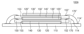
도 3a를 참조하면, 본 응용예의 반도체 패키지(100A)는 도 2a에서 설명한 바와 같이 기판(110) 상에 제1 접착층(120)을 매개로 제1 반도체 칩(130)이 탑재되고, 제1 반도체 칩(130) 상에는 제2 접착층(140)을 매개로 제2 반도체 칩(150)이 적층된다. 제2 반도체 칩(150)에는 홈(155)이 형성되어 있어 제1 반도체 칩(130)이 홈(155)에 삽입되는 형태로 제1 및 제2 반도체 칩(130,150)이 도 2a에 도시된 바와 같은 오버행 구조를 이루도록 적층된다. 제2 반도체 칩(150)에 형성된 제2 칩패드(152)와 기판(110)에 형성된 제2 기판패드(114)가 제2 와이어(170)에 의해 전기적으로 연결되므로써 제2 반도체 칩(150)은 기판(110)과 전기적으로 연결된다. 제1 반도체 칩(120)과 기판(110)은 도 1에 도시된 바와 마찬가지로 제1 와이어(도 1의 160)에 의해 전기적으로 연결된다.Referring to FIG. 3A, in the
마찬가지로, 제2 반도체 칩(150) 상에 제3 접착층(120')을 매개로 제3 반도 체 칩(130')이 적층되고, 제3 반도체 칩(130') 상에는 제4 접착층(140')을 매개로 제4 반도체 칩(150')이 적층된다. 제4 반도체 칩(150')에는 홈(155')이 형성되어 있어 제3 반도체 칩(130')이 홈(155')에 삽입되는 형태로 제3 및 제4 반도체 칩(130',150')이 도 2a에 도시된 바와 같은 오버행 구조를 이루도록 적층된다. 기판(110)에는 제3 기판패드(114')가 더 형성되어 있을 수 있다. 제4 반도체 칩(150')에 형성된 칩패드(152')와 기판(110)에 형성된 제3 기판패드(114')가 제3 와이어(170')에 의해 전기적으로 연결되므로써 제4 반도체 칩(150')은 기판(110)과 전기적으로 연결된다. 제4 반도체 칩(150') 상에는 제5 접착층(120˝)을 매개로 제5 반도체 칩(130˝)이 더 적층될 수 있다. 제3 반도체 칩(120')과 기판(110)은 도 1에 도시된 바와 마찬가지로 와이어에 의해 전기적으로 연결되며, 제5 반도체 칩(130˝)과 기판(110)과의 전기적 연결도 이와 마찬가지이다.Similarly, the third semiconductor chip 130 'is stacked on the
도 3b를 참조하면, 특히 제1 반도체 칩(130)과 제2 반도체 칩(150) 사이에 개재된 제2 접착층(140)이 제2 반도체 칩(150)의 오버행 부분을 지지하는 연장된 부분(140a)을 포함하고 있으면 오버행 부분은 더 견고히 지지된다. 제3 반도체 칩(130')과 제4 반도체 칩(150') 사이에 개재된 제4 접착층(140a)도 이와 마찬가지로 연장된 부분(140a')을 포함하고 있으면 제4 반도체 칩(150')의 오버행 부분이 더 견고하게 지지된다.Referring to FIG. 3B, an extended portion in which the second
(방법 실시예)(Method Example)
도 4a 내지 도 4d는 본 발명의 실시예에 따른 반도체 패키지를 제조하는 방 법을 도시한 단면도이다.4A through 4D are cross-sectional views illustrating a method of manufacturing a semiconductor package in accordance with an embodiment of the present invention.
도 4a를 참조하면, 기판(110)의 상면(110f)에 제1 접착층(120)을 매개로 제1 반도체 칩(130)을 실장한다. 이때, 제1 반도체 칩(130)의 활성면(130f)이 위를 향하게 한다. 기판(110)에는 다수개의 제1 기판패드(도 1의 112)와 제2 기판패드(114)가 형성되어 있다. 도 1에 도시된 바와 유사하게 제1 반도체 칩(130)과 기판(110)을 제1 와이어(도 1의 160)를 이용하여 전기적으로 연결시킨다. 제1 접착층(120)은 통상의 반도체 공정에 사용되는 액상 또는 필름 형태의 접착제로써 이루어질 수 있다.Referring to FIG. 4A, the
도 4b를 참조하면, 제1 반도체 칩(130)의 활성면(130f) 상에 제2 접착층(140)을 형성하고, 제2 반도체 칩(150)을 제1 반도체 칩(130) 상에 적층시켜 제2 반도체 칩(150)의 일부가 제1 반도체 칩(130)의 바깥으로 돌출된 이른바 오버행 구조를 이루도록 한다. 이때, 제2 반도체 칩(150)의 비활성면(150b)이 제1 반도체 칩(130)의 활성면(130f)이 서로 마주보도록 하여 비활성면(150b)에 형성된 홈(155)에 제1 반도체 칩(130)이 삽입되도록 한다. 제1 및 제2 반도체 칩(130,150)의 적층은 P방향으로의 적당한 압력을 가하여 진행할 수 있고, 제2 접착층(140)이 홈(155)에 충분히 충진될 수 있도록 수십 ℃(예; 10 ~ 80 ℃) 정도의 적당한 열을 선택적으로 가할 수 있다. 홈(155)은, 예를 들어, 화학약품 또는 플라즈마 등을 이용한 식각 공정을 이용하여 제2 반도체 칩(150)의 비활성면(150b) 일부를 제거하여 형성할 수 있다. 제2 접착층(140)은 통상의 반도체 공정에 사용되는 액상 또는 필름 형태의 접착제로써 이루어질 수 있다.Referring to FIG. 4B, the second
도 4c를 참조하면, 제2 기판패드(114)와 제2 칩패드(152)를 전기적으로 연결하는 제2 와이어(170)를 형성하여 제2 반도체 칩(150)과 기판(110)을 전기적으로 연결시켜 반도체 패키지(100)를 구현한다. 선택적으로, 에폭시 몰딩 컴파운드(EMC)와 같은 몰딩재를 이용하여 몰딩 공정을 더 진행할 수 있다. 한편, 제2 접착층(140)의 양을 상대적으로 더 늘리면 가압 또는 가열에 의해 제2 접착층(140)이 흘러 나와 도 2b에 도시된 바와 같이 제2 반도체 칩(150)의 오버행 부분을 지지하는 연장된 부분(140a)이 형성되도록 할 수 있다. Referring to FIG. 4C, a
도 4d를 참조하면, 선택적으로 제2 반도체 칩(150) 상에 제3 접착층(120')을 매개로 제3 반도체 칩(130')을 적층하고, 제3 반도체 칩(130') 상에 제4 접착층(140')을 매개로 제4 반도체 칩(150')을 더 적층할 수 있다. 또한, 제4 반도체 칩(150') 상에는 제5 접착층(120˝)을 매개로 제5 반도체 칩(130˝)을 더 적층할 수 있다. 이에 따라, 다수개의 반도체 칩이 오버행 구조로 적층된 반도체 패키지(100A)가 구현된다.Referring to FIG. 4D, the
한편, 제4 반도체 칩(150')에 홈(155')을 형성하여 제3 반도체 칩(130')이 홈(155')에 삽입되도록 하여 제3 및 제4 반도체 칩(130',150')이 오버행 구조를 이루도록 적층한다. 제4 반도체 칩(150')에 형성된 칩패드(152')와 기판(110)에 형성된 제3 기판패드(114')를 제3 와이어(170')로써 연결하여 제4 반도체 칩(150')을 기판(110)과 전기적으로 연결한다. 제3 반도체 칩(120')과 기판(110)은 도 1에 도시된 바와 유사하게 와이어에 의해 전기적으로 연결하고, 제5 반도체 칩(130˝)과 기판(110)과의 전기적 연결도 이와 마찬가지이다.Meanwhile, the grooves 155 'are formed in the fourth semiconductor chip 150' so that the third semiconductor chip 130 'is inserted into the grooves 155' so that the third and fourth semiconductor chips 130 'and 150' are inserted into the
여기에 있어서도 도 4c에서 설명한 바와 같이 제2 접착층(140) 및 제4 접착층(140')의 양을 늘려 도 3b에 도시된 바와 같이 제2 반도체 칩(150)의 오버행 부분을 지지하는 부분(140a)과 제4 반도체 칩(150')의 오버행 부분을 지지하는 부분(140a')을 더 형성할 수 있다.In this case, as illustrated in FIG. 4C, the amount of the second
이상의 발명의 상세한 설명은 개시된 실시 상태로 본 발명을 제한하려는 의도가 아니며, 본 발명의 요지를 벗어나지 않는 범위 내에서 다양한 다른 조합, 변경 및 환경에서 사용할 수 있다. 첨부된 청구범위는 다른 실시 상태도 포함하는 것으로 해석되어야 할 것이다.The foregoing detailed description is not intended to limit the invention to the disclosed embodiments, and may be used in various other combinations, modifications, and environments without departing from the spirit of the invention. The appended claims should be construed to include other embodiments.
이상에서 상세히 설명한 바와 같이, 본 발명에 의하면, 오버행을 이루는 상부칩에 하부칩이 삽입되는 홈을 형성하여 상부칩과 하부칩을 맞물려 끼우는 방법으로 반도체 칩들이 적층된다. 그리고, 상하부 칩들이 맞물리는 부분이 접착층에 의해 고정되도록 하며, 접착층이 상하부 칩들 사이의 틈으로 밀려나와 오버행 부분을 지지하게 한다. 이에 따라, 반도체 칩들이 오버행 구조를 이루도록 적층되더라도 강도가 약화되지 않아 칩들의 파손없이 적층할 수 있는 효과가 있다.As described above in detail, according to the present invention, the semiconductor chips are stacked in such a manner as to form a groove into which the lower chip is inserted into the upper chip forming the overhang, thereby engaging the upper chip with the lower chip. Then, the portion where the upper and lower chips are engaged is fixed by the adhesive layer, and the adhesive layer is pushed into the gap between the upper and lower chips to support the overhang portion. Accordingly, even when the semiconductor chips are stacked to form an overhang structure, the strength is not weakened, so that the chips can be stacked without breakage of the chips.
Claims (13)
Priority Applications (1)
| Application Number | Priority Date | Filing Date | Title |
|---|---|---|---|
| KR1020070044110A KR20080098797A (en) | 2007-05-07 | 2007-05-07 | Semiconductor Package and Manufacturing Method |
Applications Claiming Priority (1)
| Application Number | Priority Date | Filing Date | Title |
|---|---|---|---|
| KR1020070044110A KR20080098797A (en) | 2007-05-07 | 2007-05-07 | Semiconductor Package and Manufacturing Method |
Publications (1)
| Publication Number | Publication Date |
|---|---|
| KR20080098797A true KR20080098797A (en) | 2008-11-12 |
Family
ID=40286030
Family Applications (1)
| Application Number | Title | Priority Date | Filing Date |
|---|---|---|---|
| KR1020070044110A Withdrawn KR20080098797A (en) | 2007-05-07 | 2007-05-07 | Semiconductor Package and Manufacturing Method |
Country Status (1)
| Country | Link |
|---|---|
| KR (1) | KR20080098797A (en) |
Cited By (1)
| Publication number | Priority date | Publication date | Assignee | Title |
|---|---|---|---|---|
| KR20150081646A (en) * | 2014-01-06 | 2015-07-15 | 에스케이하이닉스 주식회사 | Chip stack package and method of fabricating the chip stack package |
-
2007
- 2007-05-07 KR KR1020070044110A patent/KR20080098797A/en not_active Withdrawn
Cited By (1)
| Publication number | Priority date | Publication date | Assignee | Title |
|---|---|---|---|---|
| KR20150081646A (en) * | 2014-01-06 | 2015-07-15 | 에스케이하이닉스 주식회사 | Chip stack package and method of fabricating the chip stack package |
Similar Documents
| Publication | Publication Date | Title |
|---|---|---|
| JP5529371B2 (en) | Semiconductor device and manufacturing method thereof | |
| JP4498403B2 (en) | Semiconductor device and semiconductor memory device | |
| KR100574223B1 (en) | Multichip Package and Manufacturing Method | |
| US20090166839A1 (en) | Semiconductor stack device and mounting method | |
| JPH11354669A (en) | Ball grid array type semiconductor package and method of manufacturing the same | |
| JP2003078105A (en) | Stack chip module | |
| TW201312723A (en) | Chip package structure and method of manufacturing same | |
| CN100452396C (en) | Semiconductor device and manufacturing method thereof | |
| KR20060125574A (en) | Epoxy bumps for overhang die | |
| US20090057916A1 (en) | Semiconductor package and apparatus using the same | |
| JP4766050B2 (en) | Method for manufacturing electronic circuit device | |
| US7199465B2 (en) | Wire bonding system and method of use | |
| JP2013069988A (en) | Semiconductor device and method of manufacturing the same | |
| JP2006128169A (en) | Semiconductor device and manufacturing method of semiconductor device | |
| KR20080098797A (en) | Semiconductor Package and Manufacturing Method | |
| KR101046251B1 (en) | Stacked Semiconductor Packages | |
| KR100650728B1 (en) | Stack Package and Manufacturing Method | |
| KR100947146B1 (en) | Semiconductor package | |
| CN101409265B (en) | Substrate for a semiconductor package structure, semiconductor package structure and manufacturing method thereof | |
| KR20110056768A (en) | Semiconductor package | |
| JP4602223B2 (en) | Semiconductor device and semiconductor package using the same | |
| JP2016063002A (en) | Semiconductor device and method of manufacturing the same | |
| KR101019706B1 (en) | Semiconductor package and manufacturing method thereof | |
| JP2012227320A (en) | Semiconductor device | |
| CN103426872A (en) | Semiconductor packaging part and manufacturing method thereof |
Legal Events
| Date | Code | Title | Description |
|---|---|---|---|
| PA0109 | Patent application |
St.27 status event code: A-0-1-A10-A12-nap-PA0109 |
|
| PG1501 | Laying open of application |
St.27 status event code: A-1-1-Q10-Q12-nap-PG1501 |
|
| PC1203 | Withdrawal of no request for examination |
St.27 status event code: N-1-6-B10-B12-nap-PC1203 |
|
| WITN | Application deemed withdrawn, e.g. because no request for examination was filed or no examination fee was paid | ||
| R18-X000 | Changes to party contact information recorded |
St.27 status event code: A-3-3-R10-R18-oth-X000 |
|
| P22-X000 | Classification modified |
St.27 status event code: A-2-2-P10-P22-nap-X000 |