KR20080098791A - Coating film forming apparatus - Google Patents
Coating film forming apparatus Download PDFInfo
- Publication number
- KR20080098791A KR20080098791A KR1020070044099A KR20070044099A KR20080098791A KR 20080098791 A KR20080098791 A KR 20080098791A KR 1020070044099 A KR1020070044099 A KR 1020070044099A KR 20070044099 A KR20070044099 A KR 20070044099A KR 20080098791 A KR20080098791 A KR 20080098791A
- Authority
- KR
- South Korea
- Prior art keywords
- coating film
- filter
- film
- liquid material
- forming apparatus
- Prior art date
- Legal status (The legal status is an assumption and is not a legal conclusion. Google has not performed a legal analysis and makes no representation as to the accuracy of the status listed.)
- Withdrawn
Links
Images


Classifications
-
- G—PHYSICS
- G03—PHOTOGRAPHY; CINEMATOGRAPHY; ANALOGOUS TECHNIQUES USING WAVES OTHER THAN OPTICAL WAVES; ELECTROGRAPHY; HOLOGRAPHY
- G03F—PHOTOMECHANICAL PRODUCTION OF TEXTURED OR PATTERNED SURFACES, e.g. FOR PRINTING, FOR PROCESSING OF SEMICONDUCTOR DEVICES; MATERIALS THEREFOR; ORIGINALS THEREFOR; APPARATUS SPECIALLY ADAPTED THEREFOR
- G03F7/00—Photomechanical, e.g. photolithographic, production of textured or patterned surfaces, e.g. printing surfaces; Materials therefor, e.g. comprising photoresists; Apparatus specially adapted therefor
- G03F7/16—Coating processes; Apparatus therefor
- G03F7/162—Coating on a rotating support, e.g. using a whirler or a spinner
-
- H10P72/0402—
Landscapes
- Physics & Mathematics (AREA)
- General Physics & Mathematics (AREA)
- Materials For Photolithography (AREA)
- Exposure Of Semiconductors, Excluding Electron Or Ion Beam Exposure (AREA)
- Coating Apparatus (AREA)
Abstract
본 발명은 도포막 형성 장치에 관한 것으로, 액상의 재료 물질을 이용하여 반도체 제조 공정에서 도포막을 형성하기 위하한 도포막 형성 장치에 있어서, 상기 재료 물질에 포함된 불순물을 제거하되, 소수성 물질로 형성된 필터를 포함하는 제1 여과부 및 상기 제1 여과부와 소통 가능하게 연결되고, 상기 재료 물질에 포함된 불순물을 제거하되, 친수성 물질로 형성된 필터를 포함하는 제2 여과부를 포함하는 것을 특징으로 하기 때문에, 액상의 재료 물질에 포함된 불순물을 보다 효과적으로 제거할 수 있다. The present invention relates to a coating film forming apparatus, wherein the coating film forming apparatus for forming a coating film in a semiconductor manufacturing process using a liquid material material, the impurities contained in the material material is removed, And a first filtration unit including a filter and a second filtration unit communicatively connected to the first filtration unit to remove impurities included in the material material and including a filter formed of a hydrophilic material. Therefore, impurities contained in the liquid material material can be removed more effectively.
Description
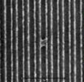
도 1a 내지 도 1d는 액상 물질에 포함된 불순물에 의해 도포막에 발생된 결함을 나타낸 SEM(Scanning Electron Microscope) 사진이다.1A to 1D are SEM (Scanning Electron Microscope) photographs showing defects generated in a coating film by impurities included in a liquid material.
도 2는 본 발명에 따른 도포막 형성 장치를 도시한 개략도이다.2 is a schematic view showing a coating film forming apparatus according to the present invention.
<도면의 주요 부분에 대한 부호 설명><Description of the symbols for the main parts of the drawings>
202 : 제1 여과부 204 : 제1 필터202: First Filter Part 204: First Filter
206 : 제2 여과부 208 : 제2 필터206: second filter 208: second filter
본 발명은 도포막 형성 장치에 관한 것으로, 보다 상세하게는 도포막을 형성하기 위하여 반도체 기판에 도포하는 액상의 물질에 포함된 불순물을 효과적으로 걸러낼 수 있는 도포막 형성 장치에 관한 것이다.The present invention relates to a coating film forming apparatus, and more particularly, to a coating film forming apparatus capable of effectively filtering out impurities contained in a liquid substance applied to a semiconductor substrate to form a coating film.
각종 전자 기기에 사용되고 있는 반도체 장치는 일반적으로 반도체막, 절연막 및 도전막 등의 박막으로 구성된다. 이들의 박막 형성에는, 주로 CVD (Chemical Vapor Deposition)법이나 스퍼터링법이 이용되고 있다. CVD 법은 상압 CVD, 감압 CVD, 플라즈마 CVD 등을 포함하고 스퍼터링법은 AC형과 DC형을 포함한다. AC형은 절연막 형성에 이용되고, DC형은 도전막 형성에 이용된다. 이러한 CVD 법이나 스퍼터링법에는, 진공 장치, 플라즈마 등을 발생시키는 전원 장치, 박막 형성을 위한 가스 공급 장치 및 기판 온도의 제어 등이 필요하다. 또한, 박막 형성에 이용되는 가스로서는, 독성, 가연성, 자연 발화성 등의 성질을 가지는 것이 많아서 가스의 누설 검지기, 배기가스를 무해화하는 유해물질 제거 장치, 가스 용기나 가스 배관부의 배기계 등에 대하여 안전성을 확보하기 위해서는 여러가지 부대 설비가 요구 된다. 또한, 이들의 방법에서는, 기체 상태의 소스로부터 고체 상태의 박막이 형성되기 때문에 생산성이 좋지 않은 문제도 있다. BACKGROUND Semiconductor devices used in various electronic devices generally consist of thin films such as semiconductor films, insulating films and conductive films. CVD (Chemical Vapor Deposition) method and sputtering method are mainly used for these thin film formation. CVD methods include atmospheric pressure CVD, reduced pressure CVD, plasma CVD and the like, and sputtering methods include AC type and DC type. The AC type is used for forming the insulating film, and the DC type is used for forming the conductive film. Such a CVD method or a sputtering method requires a power supply device for generating a vacuum device, a plasma or the like, a gas supply device for forming a thin film, control of a substrate temperature, and the like. In addition, the gas used for thin film formation has many properties such as toxicity, flammability, spontaneous flammability, and the like. Therefore, safety of a gas leak detector, a harmful substance removal device that harms exhaust gas, a gas container or an exhaust system of a gas pipe, etc. To secure them, various additional equipment is required. Moreover, in these methods, since a thin film of a solid state is formed from a gaseous source, there also exists a problem that productivity is not good.
이에 따라, 액상 재료를 기판에 도포하여 도포막을 형성하고, 그 도포막에 대해 소정의 처리공정을 실시함으로써 원하는 박막을 형성하는 방법이 제안되고 있다. 그 박막의 기본 형성 공정은 반도체 기판상에 액상 재료를 도포하여 도포막을 형성하는 도포 공정과, 그 도포막에 대해 소정의 처리 공정을 실시하여 원하는 박막을 얻는 막처리 공정을 포함한다. 이 공정에 의하면, 소형의 저가 장치를 사용하여 높은 생산성과 저비용으로 박막이 형성될 수 있어 저비용의 박막 장치가 제조될 수 있다. 상기 도포 공정으로서는, 스핀 코팅법 또는 액체 토출법(잉크젯법)에 의한 도포 방법이 일반적으로 채용된다. Accordingly, a method of forming a desired thin film by applying a liquid material to a substrate to form a coating film and performing a predetermined treatment step on the coating film has been proposed. The basic formation process of the thin film includes a coating step of applying a liquid material onto a semiconductor substrate to form a coating film, and a film processing step of performing a predetermined treatment step on the coating film to obtain a desired thin film. According to this process, a thin film can be formed with high productivity and low cost by using a small inexpensive device, and a low cost thin film device can be manufactured. As the coating step, a coating method by a spin coating method or a liquid ejecting method (ink jet method) is generally employed.
한편, 전술한 바와 같이 반도체 기판에 박막을 형성하기 위하여 도포막을 형성하는 경우도 있지만, 통상의 반도체 소자의 제조 공정에는, 갭필 성능을 우수하게 하기 위하여 액상의 물질로 SOG 산화막을 형성하거나 포토 레지스트와 같이 원래의 재료 물질이 액상인 물질로 포토 레지스트막을 형성하는 등 도포막을 형성하 는 다수의 공정을 포함한다. 이러한 도포막 형성 공정에서는 액상의 재료 물질에 불순물이 포함될 경우 결함이 발생되어 수율이 저하되는데, 이는 포토 레지스트를 이용하여 미세한 패턴을 형성하는 반도체 소자의 패턴 형성 공정에서 더욱 중요한 이슈가 되고 있다. 이를 하기에서 더욱 상세하게 설명한다.On the other hand, as described above, a coating film may be formed in order to form a thin film on a semiconductor substrate. However, in a conventional semiconductor device manufacturing process, an SOG oxide film is formed of a liquid material or a photoresist and Likewise, a plurality of processes for forming a coating film, such as forming a photoresist film with a liquid material of the original material material, are included. In the coating film forming process, when impurities are included in the liquid material material, defects are generated and the yield is lowered. This becomes a more important issue in the pattern forming process of the semiconductor device forming a fine pattern using a photoresist. This will be described in more detail below.
먼저 패턴을 형성하기 위한 소정의 피식각층, 예를 들면 실리콘막, 절연막, 또는 도전막 위에 액상의 반사 방지막을 도포한다. 포토 레지스트 막의 하부막층의 광학적 성질 및 감광막 두께의 변동에 의한 정재파(standing wave), 반사 노칭(reflective notching)과 상기 하부막으로부터의 회절광 및 반사광에 의한 포토레지스트 패턴의 CD(critical dimension)의 변동이 불가피하게 일어난다. 따라서 노광원으로 사용하는 빛의 파장대에서 광흡수를 잘하는 물질을 도입하여 하부막층에서 반사를 막을 수 있는 막을 하부막과 포토레지스트 사이에 도입하게 되었는바, 이 막이 반사방지막이다. 특히, 상기 광원으로부터 자외선의 빛을 받게 되면, 이러한 자외선이 포토 레지스트 박막을 투과하게 되고, 이에 따라, 포토 레지스트 박막의 하부에 들어온 빛이 산란 또는 반사하게 되는데, 반사 방지막은 이와 같이 산란, 반사되는 빛을 흡수할 수 있으므로, 포토 레지스트의 미세 가공에 직접적으로 영향을 미칠 수 있게 되는 것이다.First, a liquid antireflection film is applied over a predetermined etching target layer for forming a pattern, for example, a silicon film, an insulating film, or a conductive film. Variation of CD (critical dimension) of the photoresist pattern by standing wave, reflective notching and diffraction light and reflected light from the lower film due to the optical properties of the lower layer of the photoresist film and the photosensitive film thickness This inevitably happens. Therefore, a material that absorbs light well in the wavelength range of light used as an exposure source is introduced between the lower film and the photoresist to prevent reflection in the lower film layer. This film is an antireflection film. In particular, when the ultraviolet light is received from the light source, the ultraviolet light is transmitted through the photoresist thin film, and thus light entering the lower portion of the photoresist thin film is scattered or reflected, and the antireflection film is scattered and reflected in this manner. Since it can absorb light, it can directly affect the fine processing of the photoresist.
그리고, 반사 방지막이 형성된 상기 웨이퍼상에 액상의 포토 레지스트를 스핀방식에 의해 균일하게 도포하여 포토 레지스트막을 형성한다. 포토 레지스트란 특정 파장대의 빛을 받으면 노광(photo exposure) 반응을 하는 일종의 감광 고분자 화합물(photosensitive polymer)이다. 이때 노광 반응이라 함은 포토 레지스트의 일정 부분이 노광 되었을 때 노광된 부분의 폴리머(polymer) 사슬이 끊어지거나 혹은 더 강하게 결합하는 것을 의미한다. 일반적으로, 포토 레지스트는 노광된 부분의 폴리머 결합 사슬이 끊어지는 포지티브(positive) 포토 레지스트와, 노광되지 않은 부분의 폴리머 결합 사슬이 끊어지는 네거티브(negative) 포토 레지스트로 구분된다. 즉, 후속하는 현상 공정을 통해 포티지브 포토 레지스트는 노광지역이 현상되어 비노광지역의 패턴이 남게 되고, 네거티브 포토 레지스트는 비노광지역이 현상되어 노광지역의 패턴이 남게 된다. 이어서, 포토 레지스트막 상부에 액상의 탑 코터(top coater)를 스핀 방식에 의해 균일하게 도포하여 막을 형성한다. 이후에, 소프트 베이크(soft bake)를 실시하고 노광 공정 및 현상 공정을 실시하여 포토 레지스트 패턴의 형성을 완료한다.A liquid photoresist is uniformly applied by the spin method on the wafer on which the antireflection film is formed to form a photoresist film. A photoresist is a kind of photosensitive polymer that undergoes a photo exposure reaction upon receiving light of a specific wavelength band. In this case, the exposure reaction means that the polymer chain of the exposed portion is broken or more strongly bonded when a portion of the photoresist is exposed. In general, photoresists are classified into positive photoresist, in which the polymer bond chains of the exposed portions are broken, and negative photoresist, in which the polymer bond chains of the unexposed portions are broken. That is, through the subsequent development process, the Portage photoresist develops the exposed area to leave the pattern of the non-exposed area, and the negative photoresist develops the non-exposed area to leave the pattern of the exposed area. Subsequently, a liquid top coater is uniformly applied on the photoresist film by a spin method to form a film. Thereafter, soft bake is performed, and an exposure process and a development process are performed to complete the formation of the photoresist pattern.
그런데, 반도체 소자의 고집적화에 따라 더욱 작은 CD(Critical Dimension)의 디자인 룰(design rule)이 적용되고, 이에 따라 작은 개구 사이즈(opening size)를 가지는 콘택홀이나 작은 폭을 가지는 미세 패턴을 형성하는 기술이 요구되고 있다. 따라서 포토 리소그래피 공정시 미세하고 결함이 없는 포토 레지스트 패턴을 형성하는 것이 중요한 이슈가 되고 있다. 하지만, 웨이퍼 상에 코팅되는 액상의 물질에 포함된 불순물이 여과되어 제거되지 않고 웨이퍼 상에 그대로 형성되면 웨이퍼 상에 다양한 결함을 발생할 수 있다.However, according to the high integration of semiconductor devices, a design rule of a smaller CD (critical dimension) is applied, thereby forming a contact hole having a small opening size or a fine pattern having a small width. This is required. Therefore, in the photolithography process, forming a fine and defect-free photoresist pattern has become an important issue. However, if impurities contained in the liquid material coated on the wafer are formed on the wafer without being filtered out, various defects may occur on the wafer.
도 1a 내지 도 1d는 액상 물질에 포함된 불순물에 의해 발생된 결함을 나타낸 SEM(Scanning Electron Microscope) 사진이다.1A to 1D are SEM (Scanning Electron Microscope) photographs showing defects caused by impurities included in a liquid material.
도 1a는 액상 물질에 포함된 불순물에 의해 포토 레지스트 패턴에 전 단(shearing)이 발생하여 포토 레지스트 패턴의 일부가 소실된 사진이다. 도 1b는 액상 물질에 포함된 파티클에 의해 포토 레지스트 패턴에 미세한 기포(micro bubble)가 발생된 사진이다. 도 1c는 액상 물질에 포함된 겔 파티클(gel particle)에 의해 포토 레지스트 패턴에 원하지 않은 패턴이 형성된 사진이다. 도 1d는 액상 물질에 포함된 불순물에 의해 반사 방지막이 변성(change)되어 결함이 발생된 사진이다.FIG. 1A is a photograph in which part of the photoresist pattern is lost due to shearing of the photoresist pattern due to impurities included in the liquid material. FIG. 1B is a photograph in which micro bubbles are generated in a photoresist pattern by particles included in a liquid material. 1C is a photograph in which an unwanted pattern is formed on a photoresist pattern by gel particles included in a liquid material. 1D is a photograph in which a defect is generated by changing an anti-reflection film by impurities included in a liquid material.
본 발명은 웨이퍼 상에 액상 물질을 도포하여 막을 형성할 때, 액상 물질에 포함된 불순물을 효과적으로 제거하여 도포막에 결함이 발생되는 것을 방지할 수 있다.According to the present invention, when a liquid material is coated on a wafer to form a film, impurities included in the liquid material may be effectively removed to prevent defects in the coated film.
본 발명에 따른 도포막 형성 장치는, 액상의 재료 물질을 이용하여 반도체 제조 공정에서 도포막을 형성하기 위하한 도포막 형성 장치에 있어서, 상기 재료 물질에 포함된 불순물을 제거하되, 소수성 물질로 형성된 필터를 포함하는 제1 여과부 및 상기 제1 여과부와 소통 가능하게 연결되고, 상기 재료 물질에 포함된 불순물을 제거하되, 친수성 물질로 형성된 필터를 포함하는 제2 여과부를 포함하는 것을 특징으로 한다.The coating film forming apparatus according to the present invention is a coating film forming apparatus for forming a coating film in a semiconductor manufacturing process using a liquid material material, while removing impurities contained in the material material, a filter formed of a hydrophobic material A first filtration unit comprising a and a second filtration unit is communicatively connected to the first filtration unit, to remove impurities contained in the material material, including a filter formed of a hydrophilic material.
상기 소수성 물질은 UPE(ultra-high molecular weight polyethylene) 물질을 포함할 수 있다. 상기 친수성 물질은 나일론(nylon) 물질을 포함할 수 있다. 상기 액상의 재료 물질은 유기반사막(organic BARC), 포토 레지스트, 탑 코터나 산화막 을 형성하기 위한 SOG(Spin On Glass) 물질, 실리콘 함유 무기반사 방지막(silicon contained Anti Reflection Coating)을 포함할 수 있다.The hydrophobic material may comprise an ultra-high molecular weight polyethylene (UPE) material. The hydrophilic material may include a nylon material. The liquid material material may include an organic BARC, a photoresist, a spin on glass (SOG) material for forming a top coater or an oxide film, and a silicon contained anti reflection coating.
이하, 첨부된 도면을 참조하여 본 발명의 바람직한 실시예를 설명하기로 한다. Hereinafter, with reference to the accompanying drawings will be described a preferred embodiment of the present invention.
그러나, 본 발명은 이하에서 설명하는 실시예에 한정되는 것이 아니라 서로 다른 다양한 형태로 구현될 수 있으며, 본 발명의 범위가 다음에 상술하는 실시예에 한정되는 것은 아니다. 또한, 본 발명의 기술 분야의 통상의 전문가라면 본 발명의 기술 사상의 범위 내에서 다양한 실시예가 가능함을 이해할 수 있을 것이다. 단지 본 실시예는 본 발명의 개시가 완전하도록 하며 통상의 지식을 가진 자에게 발명의 범주를 완전하게 알려주기 위해 제공되는 것이며, 본 발명의 범위는 본원의 특허 청구 범위에 의해서 이해되어야 한다.However, the present invention is not limited to the embodiments described below, but may be implemented in various forms, and the scope of the present invention is not limited to the embodiments described below. In addition, those skilled in the art will understand that various embodiments are possible within the scope of the technical idea of the present invention. Only this embodiment is provided to complete the disclosure of the present invention and to fully inform those skilled in the art, the scope of the present invention should be understood by the claims of the present application.
도 2는 본 발명에 따른 도포막 형성 장치를 도시한 개략도이다.2 is a schematic view showing a coating film forming apparatus according to the present invention.
도 2를 참조하면, 웨이퍼(212)에 도포막을 형성하기 위하여 웨이퍼(212)에 공급되는 액상의 재료 물질은 제1 여과부(202)로 유입되어 통과된다. 액상의 재료 물질은 포토 레지스트 패턴을 형성하기 위한 유기 반사 방지막(organic BARC), 포토 레지스트, 탑 코터, 산화막을 형성하기 위한 SOG(Spin On Glass) 물질, 실리콘 함유 무기반사 방지막(silicon contained Anti Reflection Coating) 등 반도체 제조 공정에서 도포막을 형성하기 위한 모든 액상의 재료 물질을 포함할 수 있다.Referring to FIG. 2, the liquid material material supplied to the
제1 여과부(202)에는 제1 필터(204)가 구비되어 액상의 재료 물질에 포함된 불순물을 제거한다. 제1 필터(204)는 0.01 내지 0.1㎛의 크기를 갖는 여과망을 포 함하며, 상기 여과망은 소수성(hydrophobic)을 가진 물질, 예를 들면 UPE(ultra-high molecular weight polyethylene)류의 물질로 형성되는 것이 바람직하다. 제1 필터(204)를 소수성 물질로 형성함으로써, 액상 물질에 포함된 겔과 파티클 등의 이물질을 효과적으로 제거할 수 있다. 이로써, 미세한 기포나 겔로 인하여 발생할 수 있는 패턴 결함을 방지할 수 있다.The
제1 여과부(202)를 통해 1차로 불순물이 여과된 액상의 재료 물질은, 제2 여과부(202)와 소통 가능하게 연결된 제2 여과부(206)로 유입되어 통과함으로써 2차로 여과된다. 제2 여과부(206)에는 제2 필터(208)가 구비되어 액상의 재료 물질에 잔여하는 불순물을 제거한다. 제2 필터(208)는 0.01 내지 0.1㎛ 크기 갖는 여과망으로 구성되며, 상기 여과망은 친수성(hydrophilic)을 가진 물질, 예를 들면 나일론(nylon) 류의 물질로 형성되는 것이 바람직하다. 제2 필터(208)를 친수성 물질로 형성함으로써, 제1 여과부(202)를 통해 소수성 필터를 통해 여과되지 못하고 액상 물질에 잔여하는 불순물을 효과적으로 제거할 수 있다. 이로써, 패턴이 겹치는 마이크로-브릿지(micro bridge) 등의 패턴 결함을 방지할 수 있다.The liquid material material in which impurities are primarily filtered through the
전술한 공정을 따라 불순물이 제거된 액상의 재료 물질은 노즐(210)을 통해 웨이퍼(212) 상부로 도포되어 웨이퍼(212) 상부에 액상 물질을 이용한 막을 형성할 수 있다.According to the above-described process, the liquid material material from which impurities are removed may be applied onto the
반도체 제조 공정에서 도포막을 형성하기 위한 액상의 재료 물질에 대해 소수성 필터 또는 친수성 필터 중 단일한 필터를 사용하여 불순물을 제거할 수도 있다. 또는 액상의 재료 물질을 공급하는 펌프의 구동력 등을 변화시켜 액상 물질의 공급 압력을 변화시킴으로써 액상 물질에 포함된 불순물이 웨이퍼 상으로 공급되지 않는 방법을 작용할 수도 있다. 하지만, 이러한 경우 불순물의 완전한 제거는 불가능하다. 또한, 소수성 필터 또는 친수성 필터 중 단일한 필터를 사용하되 필터의 여과망 크기를 더욱 미세화하여 불순물을 제거할 수도 있다. 하지만 필터의 여과망 크기를 지나치게 작게 할 경우 액상 물질의 고유 분자량 등과 매치되지 않아 패턴 결함이 발생하는 것을 방지할 수 없다. Impurities may be removed using a single filter of a hydrophobic filter or a hydrophilic filter for the liquid material material for forming the coating film in the semiconductor manufacturing process. Alternatively, the impurity contained in the liquid material may not be supplied onto the wafer by changing the driving force of the pump for supplying the liquid material material and the like to change the supply pressure of the liquid material. In this case, however, complete removal of impurities is impossible. In addition, a single filter of hydrophobic or hydrophilic filters may be used, but impurities may be removed by further minimizing the filter network size. However, if the filter screen size of the filter is too small, it does not match the intrinsic molecular weight of the liquid material and thus cannot prevent the occurrence of pattern defects.
하지만 본 발명은 액상 물질을 소수성 필터와 친수성 필터를 통해 2차에 걸쳐 여과함으로써 액상 물질에 포함된 불순물을 효과적으로 제거할 수 있다.However, the present invention can effectively remove impurities contained in the liquid material by filtering the liquid material through the hydrophobic filter and the hydrophilic filter for two times.
한편, 본 발명에서는 도포막을 형성할 때 사용되는 액상의 재료 물질을 소수성 물질로 형성된 필터를 통해 여과한 뒤 친수성 물질로 형성된 필터를 통해 여과하는 것으로 예시하였지만 이에 한정되지 않는다. 따라서 도포막을 형성할 때 사용되는 액상의 재료 물질을 친수성 물질로 형성된 필터를 통해 여과한 뒤 소수성 물질로 형성된 필터를 통해 여과하는 것도 가능하다.Meanwhile, in the present invention, the liquid material used to form the coating film is filtered through a filter formed of a hydrophobic material and then filtered through a filter formed of a hydrophilic material, but is not limited thereto. Therefore, it is also possible to filter the liquid material material used when forming the coating film through a filter formed of a hydrophilic material and then through a filter formed of a hydrophobic material.
본 발명의 도포막 형성 장치에 따르면 웨이퍼 상에 액상의 재료 물질을 도포하여 막을 형성할 때, 친수성 필터와 소수성 필터를 이용하여 액상의 재료 물질에 포함된 불순물을 2차로 제거함으로써, 액상의 재료 물질에 포함된 불순물을 보다 효과적으로 제거할 수 있다. 따라서, 도포막에 결함이 발생되는 것을 방지할 수 있다.According to the coating film forming apparatus of the present invention, when forming a film by applying a liquid material material on the wafer, the liquid material material by secondary removal of impurities contained in the liquid material material by using a hydrophilic filter and a hydrophobic filter Impurities contained in can be more effectively removed. Therefore, it can prevent that a defect arises in a coating film.
Claims (5)
Priority Applications (1)
| Application Number | Priority Date | Filing Date | Title |
|---|---|---|---|
| KR1020070044099A KR20080098791A (en) | 2007-05-07 | 2007-05-07 | Coating film forming apparatus |
Applications Claiming Priority (1)
| Application Number | Priority Date | Filing Date | Title |
|---|---|---|---|
| KR1020070044099A KR20080098791A (en) | 2007-05-07 | 2007-05-07 | Coating film forming apparatus |
Publications (1)
| Publication Number | Publication Date |
|---|---|
| KR20080098791A true KR20080098791A (en) | 2008-11-12 |
Family
ID=40286026
Family Applications (1)
| Application Number | Title | Priority Date | Filing Date |
|---|---|---|---|
| KR1020070044099A Withdrawn KR20080098791A (en) | 2007-05-07 | 2007-05-07 | Coating film forming apparatus |
Country Status (1)
| Country | Link |
|---|---|
| KR (1) | KR20080098791A (en) |
Cited By (1)
| Publication number | Priority date | Publication date | Assignee | Title |
|---|---|---|---|---|
| KR101428907B1 (en) * | 2013-01-11 | 2014-08-08 | 주식회사 코리아써키트 | Nozzle for dreg removal |
-
2007
- 2007-05-07 KR KR1020070044099A patent/KR20080098791A/en not_active Withdrawn
Cited By (1)
| Publication number | Priority date | Publication date | Assignee | Title |
|---|---|---|---|---|
| KR101428907B1 (en) * | 2013-01-11 | 2014-08-08 | 주식회사 코리아써키트 | Nozzle for dreg removal |
Similar Documents
| Publication | Publication Date | Title |
|---|---|---|
| JP3410720B2 (en) | Cleaning method for quartz substrate using conductive solution | |
| CN106547166B (en) | Pellicle assembly for photolithography process and method for manufacturing mask pellicle system | |
| TWI717437B (en) | A method of manufacturing a membrane assembly for euv lithography, a membrane assembly, a lithographic apparatus, and a device manufacturing method | |
| US20080264441A1 (en) | Method for removing residuals from photomask | |
| TW201804242A (en) | Method for EUV pellicle glue removal | |
| KR20120082432A (en) | Method for reworking a silicon-containing arc layer on a substrate | |
| US20020098709A1 (en) | Method for removing photoresist layer on wafer edge | |
| EP3371655B1 (en) | A method for manufacturing a membrane assembly and the membrane assembly | |
| JP2003173951A (en) | Method of manufacturing mask for electron beam lithography and mask blank for electron beam lithography | |
| KR20080098791A (en) | Coating film forming apparatus | |
| JP4922858B2 (en) | Pattern forming method and cleaning apparatus | |
| KR20080084274A (en) | Manufacturing Method of Semiconductor Device | |
| JP3250240B2 (en) | Method for manufacturing semiconductor device | |
| JPH0290172A (en) | Method for peeling resist pattern | |
| KR20050070436A (en) | Method for removing particle in semiconductor reticle | |
| US9588417B2 (en) | Photomask pellicle | |
| KR20080062746A (en) | Pellicle to suppress haze generation on photomask | |
| CA3008939C (en) | A method of manufacturing a membrane assembly for euv lithography, a membrane assembly, a lithographic apparatus, and a device manufacturing method | |
| KR20050059622A (en) | Wafer edge exposure apparatus | |
| TWI434142B (en) | Lithography apparatus with a fiber module | |
| KR20040110685A (en) | Dry Etching Apparatus | |
| CN101044599A (en) | Method for forming a photoresist pattern | |
| JPH05102117A (en) | Wafer processing method and wafer processing apparatus |
Legal Events
| Date | Code | Title | Description |
|---|---|---|---|
| PA0109 | Patent application |
St.27 status event code: A-0-1-A10-A12-nap-PA0109 |
|
| PG1501 | Laying open of application |
St.27 status event code: A-1-1-Q10-Q12-nap-PG1501 |
|
| PN2301 | Change of applicant |
St.27 status event code: A-3-3-R10-R13-asn-PN2301 St.27 status event code: A-3-3-R10-R11-asn-PN2301 |
|
| PC1203 | Withdrawal of no request for examination |
St.27 status event code: N-1-6-B10-B12-nap-PC1203 |
|
| WITN | Application deemed withdrawn, e.g. because no request for examination was filed or no examination fee was paid | ||
| PN2301 | Change of applicant |
St.27 status event code: A-3-3-R10-R13-asn-PN2301 St.27 status event code: A-3-3-R10-R11-asn-PN2301 |
|
| PN2301 | Change of applicant |
St.27 status event code: A-3-3-R10-R13-asn-PN2301 St.27 status event code: A-3-3-R10-R11-asn-PN2301 |
|
| P22-X000 | Classification modified |
St.27 status event code: A-2-2-P10-P22-nap-X000 |
|
| P22-X000 | Classification modified |
St.27 status event code: A-2-2-P10-P22-nap-X000 |
|
| P22-X000 | Classification modified |
St.27 status event code: A-2-2-P10-P22-nap-X000 |