KR20080098709A - Wafer transfer equipment - Google Patents
Wafer transfer equipment Download PDFInfo
- Publication number
- KR20080098709A KR20080098709A KR1020070043894A KR20070043894A KR20080098709A KR 20080098709 A KR20080098709 A KR 20080098709A KR 1020070043894 A KR1020070043894 A KR 1020070043894A KR 20070043894 A KR20070043894 A KR 20070043894A KR 20080098709 A KR20080098709 A KR 20080098709A
- Authority
- KR
- South Korea
- Prior art keywords
- wafer
- transfer
- chamber
- sensor
- unit
- Prior art date
- Legal status (The legal status is an assumption and is not a legal conclusion. Google has not performed a legal analysis and makes no representation as to the accuracy of the status listed.)
- Withdrawn
Links
Images


Classifications
-
- H—ELECTRICITY
- H10—SEMICONDUCTOR DEVICES; ELECTRIC SOLID-STATE DEVICES NOT OTHERWISE PROVIDED FOR
- H10P—GENERIC PROCESSES OR APPARATUS FOR THE MANUFACTURE OR TREATMENT OF DEVICES COVERED BY CLASS H10
- H10P72/00—Handling or holding of wafers, substrates or devices during manufacture or treatment thereof
- H10P72/30—Handling or holding of wafers, substrates or devices during manufacture or treatment thereof for conveying, e.g. between different workstations
- H10P72/33—Handling or holding of wafers, substrates or devices during manufacture or treatment thereof for conveying, e.g. between different workstations into and out of processing chamber
-
- H—ELECTRICITY
- H10—SEMICONDUCTOR DEVICES; ELECTRIC SOLID-STATE DEVICES NOT OTHERWISE PROVIDED FOR
- H10P—GENERIC PROCESSES OR APPARATUS FOR THE MANUFACTURE OR TREATMENT OF DEVICES COVERED BY CLASS H10
- H10P72/00—Handling or holding of wafers, substrates or devices during manufacture or treatment thereof
- H10P72/04—Apparatus for manufacture or treatment
- H10P72/0451—Apparatus for manufacturing or treating in a plurality of work-stations
- H10P72/0464—Apparatus for manufacturing or treating in a plurality of work-stations characterised by the construction of the transfer chamber
-
- H—ELECTRICITY
- H10—SEMICONDUCTOR DEVICES; ELECTRIC SOLID-STATE DEVICES NOT OTHERWISE PROVIDED FOR
- H10P—GENERIC PROCESSES OR APPARATUS FOR THE MANUFACTURE OR TREATMENT OF DEVICES COVERED BY CLASS H10
- H10P72/00—Handling or holding of wafers, substrates or devices during manufacture or treatment thereof
- H10P72/06—Apparatus for monitoring, sorting, marking, testing or measuring
- H10P72/0606—Position monitoring, e.g. misposition detection or presence detection
-
- H—ELECTRICITY
- H10—SEMICONDUCTOR DEVICES; ELECTRIC SOLID-STATE DEVICES NOT OTHERWISE PROVIDED FOR
- H10P—GENERIC PROCESSES OR APPARATUS FOR THE MANUFACTURE OR TREATMENT OF DEVICES COVERED BY CLASS H10
- H10P72/00—Handling or holding of wafers, substrates or devices during manufacture or treatment thereof
- H10P72/70—Handling or holding of wafers, substrates or devices during manufacture or treatment thereof for supporting or gripping
- H10P72/76—Handling or holding of wafers, substrates or devices during manufacture or treatment thereof for supporting or gripping using mechanical means, e.g. clamps or pinches
- H10P72/7602—Handling or holding of wafers, substrates or devices during manufacture or treatment thereof for supporting or gripping using mechanical means, e.g. clamps or pinches the wafers being placed on a robot blade or gripped by a gripper for conveyance
Landscapes
- Container, Conveyance, Adherence, Positioning, Of Wafer (AREA)
Abstract
웨이퍼 이송 장치는 이송 챔버, 이송부 및 센서부를 포함한다. 이송 챔버는 웨이퍼를 공정 챔버로 이송하기 위한 공간을 제공한다. 이송부는 이송 챔버 내부에 구비되며, 웨이퍼를 공정 챔버로 이송하거나 공정 챔버로부터 반송하는 역할을 한다. 센서부는 이송부의 회전 반경이 이루는 영역에 대응하는 이송 챔버에 배치되며, 이송부에 웨이퍼가 존재하는지 여부를 감지한다. 따라서, 센서부가 이송 챔버 중 반경이 웨이퍼의 외경보다 작은 중심 영역에 배치됨으로써, 웨이퍼의 존재 여부를 감지하기 위한 시간을 단축시킬 수 있다.The wafer transfer device includes a transfer chamber, a transfer unit and a sensor unit. The transfer chamber provides a space for transferring the wafer into the process chamber. The transfer unit is provided inside the transfer chamber, and serves to transfer the wafer to or from the process chamber. The sensor unit is disposed in the transfer chamber corresponding to the area formed by the rotation radius of the transfer unit, and detects whether a wafer exists in the transfer unit. Therefore, the sensor unit may be disposed in a central region of which the radius of the transfer chamber is smaller than the outer diameter of the wafer, thereby reducing the time for detecting the presence of the wafer.
Description
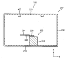
도 1은 본 발명의 일 실시예에 따른 웨이퍼 이송 장치를 나타낸 평면도이다.1 is a plan view showing a wafer transfer apparatus according to an embodiment of the present invention.
도 2는 도 1에 도시된 웨이퍼 이송 장치의 내부를 나타낸 측면도이다.FIG. 2 is a side view illustrating the inside of the wafer transfer apparatus illustrated in FIG. 1.
도 3은 도 2에 도시된 이송부, 웨이퍼 및 센서부를 구체적으로 나타낸 측면도이다. 3 is a side view illustrating in detail the transfer part, the wafer, and the sensor part shown in FIG. 2.
도 4는 도 1에 도시된 웨이퍼 이송 장치에서 웨이퍼를 감지하는 과정을 나타낸 순서도이다.FIG. 4 is a flowchart illustrating a process of detecting a wafer in the wafer transport apparatus illustrated in FIG. 1.
도 5는 도 4에 도시된 과정의 일부를 개략적으로 나타낸 평면도이다.5 is a plan view schematically illustrating a part of the process illustrated in FIG. 4.
<도면의 주요 부분에 대한 부호의 설명><Explanation of symbols for main parts of the drawings>
10 : 로딩 챔버 20 : 공정 챔버10: loading chamber 20: process chamber
30 : 웨이퍼 100 : 웨이퍼 이송 장치30: wafer 100: wafer transfer device
200 : 이송 챔버 210 : 바닥200: transfer chamber 210: floor
220 : 상판 300 : 이송부220: top plate 300: transfer unit
310 : 고정대 320 : 이송암310: holder 320: transfer arm
330 : 지지대 400 : 센서부330: support 400: sensor
410 : 제1 센서 420 : 제2 센서410: first sensor 420: second sensor
본 발명은 웨이퍼 이송 장치에 관한 것으로써, 더욱 상세하게는 웨이퍼를 공정 챔버로 이송하는 웨이퍼 이송 장치에 관한 것이다.The present invention relates to a wafer transfer device, and more particularly, to a wafer transfer device for transferring a wafer to a process chamber.
일반적으로, 반도체 소자는 실리콘 웨이퍼 상에 전기 소자들을 포함하는 전기적인 회로를 형성하는 팹(Fabrication) 공정과, 상기 팹 공정에서 형성된 반도체 소자들의 전기적인 특성을 검사하기 위한 EDS(electrical die sorting) 공정과, 상기 반도체 소자들을 각각 에폭시 수지로 봉지하고 개별화시키기 위한 패키지 조립 공정을 통해 제조된다.In general, a semiconductor device includes a fabrication process for forming an electrical circuit including electrical devices on a silicon wafer, and an electrical die sorting process for inspecting electrical characteristics of the semiconductor devices formed in the fabrication process. And, the semiconductor devices are each manufactured by a package assembly process for encapsulating and individualizing the epoxy resin.
상기와 같은 공정들은 상기 반도체 소자가 오염으로 인해 전기적인 불량이 발생되는 것을 방지하기 위하여 고 진공 상태에서 진행된다. 즉, 상기 실리콘 웨이퍼는 고 진공 상태가 유지되는 챔버들로 이송된다. Such processes are performed in a high vacuum state in order to prevent electrical failure of the semiconductor device due to contamination. That is, the silicon wafer is transferred to chambers in which a high vacuum is maintained.
또한, 상기 공정들은 매우 정밀하게 진행되므로, 상기 실리콘 웨이퍼의 이송은 정밀 제어가 가능한 별도의 이송부를 통해 진행된다. 여기서, 상기 이송부도 고 진공 상태의 챔버에 설치된다. 즉, 상기 실리콘 웨이퍼는 상기 이송부가 챔버를 중심으로 회전하면서 주위의 다른 챔버들로 이송된다. In addition, since the processes are performed very precisely, the transfer of the silicon wafer is performed through a separate transfer unit capable of precise control. Here, the transfer unit is also installed in the chamber in a high vacuum state. That is, the silicon wafer is transferred to other chambers around as the transfer part rotates about the chamber.
이때, 상기 실리콘 웨이퍼는 실질적으로, 상기 이송부에 로딩되어 이송되는지를 확인하기 위하여 센서부가 사용된다. 상기 센서부는 상기 이송부가 설치된 챔버에 배치된다.At this time, the silicon wafer is substantially used in the sensor unit to check whether the transfer is loaded. The sensor unit is disposed in a chamber in which the transfer unit is installed.
그러나, 상기 센서부는 위치가 상기 이송부의 회전 반경에서 멀리 떨어져 있 기 때문에, 상기 실리콘 웨이퍼의 존재 여부를 감지하기 위해서는 상기 이송부를 추가적으로 작동시켜 상기 센서부까지 이송해야 하는 문제점을 갖는다. 이로써, 전체적인 공정 시간이 증가하게 되는 원인이 된다.However, since the sensor part is located far from the rotation radius of the transfer part, in order to detect the presence or absence of the silicon wafer, the sensor part needs to be additionally operated and transferred to the sensor part. This causes the overall process time to increase.
따라서, 본 발명은 이와 같은 문제점을 감안한 것으로써, 본 발명의 목적은 센서부의 배치 위치를 변경하여 웨이퍼를 감지하는 시간을 단축할 수 있는 웨이퍼 이송 장치를 제공하는 것이다. Accordingly, the present invention has been made in view of such a problem, and an object of the present invention is to provide a wafer transport apparatus capable of shortening the time for sensing a wafer by changing the arrangement position of the sensor portion.
상술한 본 발명의 목적을 달성하기 위하여, 일 실시예에 따른 웨이퍼 이송 장치는 이송 챔버, 이송부 및 센서부를 포함한다. 상기 이송 챔버는 웨이퍼를 공정 챔버로 이송하기 위한 공간을 제공한다. 상기 이송부는 상기 이송 챔버 내부에 구비되며, 상기 웨이퍼를 상기 공정 챔버로 이송하거나 상기 공정 챔버로부터 반송하는 역할을 한다. 상기 센서부는 상기 이송부의 회전 반경이 이루는 영역에 대응하는 상기 이송 챔버에 배치되며, 상기 이송부에 상기 웨이퍼가 존재하는지 여부를 감지한다.In order to achieve the above object of the present invention, a wafer transfer apparatus according to an embodiment includes a transfer chamber, a transfer unit and a sensor unit. The transfer chamber provides a space for transferring the wafer to the process chamber. The transfer unit is provided inside the transfer chamber, and serves to transfer the wafer to or from the process chamber. The sensor unit is disposed in the transfer chamber corresponding to an area formed by the rotation radius of the transfer unit, and detects whether the wafer exists in the transfer unit.
상기 센서부는 상기 웨이퍼의 상부 중 상기 영역의 가장자리에 대응하는 위치에 배치된다. 이와 달리, 상기 센서부는 상기 웨이퍼의 상부 중 상기 이송부의 외곽에 대응하는 위치에 배치될 수 있다. The sensor unit is disposed at a position corresponding to an edge of the region of the upper portion of the wafer. In contrast, the sensor unit may be disposed at a position corresponding to the outside of the transfer unit among the upper portions of the wafer.
또한, 상기 센서부는 상기 웨이퍼의 상부 및 하부 중 어느 하나에 대응되는 상기 이송 챔버의 내벽에 배치될 수 있다. In addition, the sensor unit may be disposed on an inner wall of the transfer chamber corresponding to any one of the upper and lower portions of the wafer.
이러한 웨이퍼 이송 장치에 따르면, 웨이퍼의 존재를 감지하기 위한 센서부를 이송부의 회전 반경이 이루는 영역에 대응하는 이송 챔버에 배치시킴으로써, 웨이퍼가 실질적으로, 이송되는지를 감지하는 공정 시간을 단축시킬 수 있다.According to such a wafer transfer apparatus, by placing the sensor unit for detecting the presence of the wafer in the transfer chamber corresponding to the region of the rotation radius of the transfer unit, it is possible to shorten the process time for detecting whether the wafer is substantially transferred.
이하, 첨부한 도면을 참조하여, 본 발명의 바람직한 실시예들을 상세하게 설명하고자 한다.Hereinafter, exemplary embodiments of the present invention will be described in detail with reference to the accompanying drawings.
도 1은 본 발명의 일 실시예에 따른 웨이퍼 감지 장를 나타낸 평면도이며, 도 2는 도 1에 도시된 웨이퍼 이송 장치의 내부를 나타낸 측면도이다.1 is a plan view showing a wafer sensing field according to an embodiment of the present invention, Figure 2 is a side view showing the inside of the wafer transfer apparatus shown in FIG.
도 1 및 도 2를 참조하면, 본 발명의 일 실시예에 따른 웨이퍼 이송 장치(100)는 이송 챔버(200), 이송부(300) 및 센서부(400)를 포함한다. 1 and 2, a
상기 이송 챔버(200)의 내부에는 인접하게 배치된 로딩 챔버(10) 또는 공정 챔버(20)로부터 이송된 웨이퍼(30)가 배치된다. 여기서, 상기 웨이퍼(30)는 반도체 소자에 핵심 부품으로 사용되는 실리콘 재질의 얇은 단결정 판을 의미한다. The
상기 로딩 챔버(10)는 카셋 구조로 되어 있어, 복수의 상기 웨이퍼(30)들을 보관하는 챔버이다. 상기 공정 챔버(20)는 상기 웨이퍼(30)를 통해 반도체 소자를 제작하기 위한 실질적인 공정이 진행되는 챔버이다. 예를 들어, 상기 공정 챔버(20)에서는 사진, 식각 또는 노광 공정이 이루어질 수 있다. 즉, 상기 공정 챔버(20)는 상기 이송 챔버(200)의 주위에 복수 개가 배치될 수 있다. 이를 위해, 상기 이송 챔버(200)는 주위에 복수 개의 입구가 형성될 수 있다.The
상기 이송 챔버(200)는 내부가 고 진공 상태를 유지한다. 이를 위해, 상기 이송 챔버(200)는 호스와 같은 연결 통로를 통해 외부의 진공 펌프(미도시)와 기계적으로 연결될 필요성이 있다. 이로써, 미세 먼지가 상기 반도체 소자, 즉 상기 웨이퍼(30)에 접촉되는 것을 미연에 방지할 수 있다. 즉, 상기 반도체 소자가 상기 미세 먼지로 인하여 전기적인 특성이 변하는 것을 방지할 수 있다. The
상기 이송부(300)는 상기 이송 챔버(200)의 내부에 배치 고정된다. 상기 이송부(300)는 상기 웨이퍼(30)를 상기 로딩 챔버(10) 또는 상기 공정 챔버(20)에서 로딩하여 상기 로딩 챔버(10), 상기 이송 챔버(200) 또는 상기 공정 챔버(20)로 이송시키는 역할을 한다. 상기의 이송은 실질적으로, 기설정된 프로그램에 의해 자동적으로 동작할 수도 있고, 경우에 따라, 작업자에 의해 제어될 수도 있다. 이러한 상기 이송부(300)는 산업 현장에서 널리 사용되는 로봇(robot) 장치를 의미할 수 있다.The
구체적으로, 상기 이송부(300)는 상기 이송 챔버(200)의 바닥(210)에 고정된 고정대(310), 상기 고정대(310)에 결합되어 평면 방향(x, y)을 따라 유동하는 이송암(320) 및 상기 이송암(320)에 결합된 지지대(330)를 포함한다.In detail, the
상기 고정대(310)는 상기 이송부(300)의 버팀 역할을 한다. 상기 고정대(310)는 도면에는 도시하지 않았지만, 제1 고정대(미도시)와 제2 고정대(미도시)를 포함하여 상기 평면 방향(x, y)에 수직한 수직 방향(z)을 따라 유동할 수 있다. 여기서, 상기 제1 고정대 및 상기 제2 고정대는 길이 조정이 가능하도록 하기 위해 소정의 차이로 서로 다른 외경을 가지면서 결합될 수 있다. The
이때, 상기 제1 고정대와 상기 제2 고정대의 유동은 실질적으로, 정밀하게 제어가 가능하면서 오염 가능성이 적은 공압 방식을 사용하는 것이 바람직할 수 있다. 하지만, 상기 이송 챔버(200)의 사이즈가 매우 방대하여 제1 고정대와 제2 고정대에 큰 동력이 필요하다면 유압 방식을 사용할 수도 있다.In this case, it may be preferable to use a pneumatic method in which the flow of the first and second fixing rods is substantially controllable and less likely to be contaminated. However, if the
상기 이송암(320)은 실질적으로, 상기 웨이퍼(30)를 이송시키는 역할을 한다. 상기 이송암(320)은 상기 이송부(300)가 로봇 장치일 경우, 로봇암으로 통용될 수 있다. 상기 이송암(320)은 도면에는 도시하지 않았지만, 상기 평면 방향(x, y)을 따라 자유 자재로 유동하기 위하여 적어도 두 개 이상으로 분리된 구조를 갖는 것이 바람직하다. 이때, 상기 분리된 이송암(320)의 연결 부위는 엘보우(elbow) 구조를 가질 수 있다. 또한, 상기 분리된 이송암(320)은 각각 길이 조정이 가능하도록 다시 두 개로 분리될 수 있다. 이에는, 상기 고정대(310)와 같은 원리가 적용될 수 있다. 또한, 상기 이송암(320)은 상기 엘보우 구조에 별도의 수직 로드를 장착하여 수직 방향(z)을 따라 유동하도록 할 수도 있다.The
상기 지지대(330)는 실질적으로, 상기 웨이퍼(30)와 접촉하여 상기 웨이퍼(30)를 지지하는 역할을 한다. 이때, 상기 지지대(330)는 상기 웨이퍼(30)의 오염을 최대한 방지하기 위하여 접촉 면적을 최소화하는 것이 바람직하다. 이를 위해, 상기 지지대(330)는 포크(fork) 형상을 가질 수 있다. 이와 달리, 상기 지지대(330)는 상기 웨이퍼(30)와 접촉 지지하는 적어도 세 개의 지지점을 가진 형상일 수 있다.The
또한, 상기 지지대(330)는 보다 안정적으로, 상기 웨이퍼(30)를 지지하기 위하여 상기 웨이퍼(30)와 마주보는 면에 진공홀이 형성될 수 있다. 이와 달리, 상기 지지대(330)는 상기 웨이퍼(30)와의 마찰 지수를 높이기 위하여 상기 웨이퍼(30)와 마주보는 면에 고무와 같이, 마찰 계수가 높은 물질을 도포할 수도 있다. In addition, the
상기 센서부(400)는 상기 이송 챔버(200) 내에 배치되어 상기 웨이퍼(30)가 실질적으로, 상기 지지대(330)에 안착되었는지 그 존재 여부를 감지한다. 구체적으로, 상기 센서부(400)는 상기 웨이퍼(30)의 상부에 배치된다. 이에 대한 바람직한 구조는 상기 센서부(400)를 상기 이송 챔버(200) 중 상기 이송부(300)가 고정된 바닥(210)과 반대되는 상판(220)에 고정하는 것이다. 이는, 상기 웨이퍼(30)가 상기 지지대(330)의 상부에 배치되어 있기 때문이다. 이와 달리, 상기 웨이퍼(30)가 상기 지지대(330)의 하부에 배치되어 있을 경우, 상기 센서부(400)는 상기 이송 챔버(200)의 상기 바닥(210)에 배치될 수 있다. 또한, 상기 센서부(400)는 별도의 센서 로드를 상기 이송 챔버(200)의 측벽(230)에 연결하여 상기 센서 로드에 고정 배치될 수 있다.The
상기 센서부(400)는 상기 이송 챔버(200)의 중심 영역(CA)에 배치된다. 이는, 상기 웨이퍼(30)가 상기 로딩 챔버(10)로부터 상기 이송 챔버(200) 이송된 후, 상기 중심 영역(CA)에서 회전 또는 일시 정지한 다음, 다른 상기 공정 챔버(20)로 이동하기 때문이다. 즉, 상기 중심 영역(CA)은 상기 웨이퍼(30)가 회전 또는 일시 정지한 위치를 의미한다. 다시 말해, 상기 중심 영역(CA)은 상기 이송부의 회전 반경이 이루는 영역과 실질적으로 동일하다. The
상기 중심 영역(CA)은 평면(x, y)적으로 보았을 때, 원 형상을 갖는다. 이에, 상기 이송부(300)는 상기 중심 영역(CA)의 중앙에 배치 고정될 수 있다. 상기 중심 영역(CA)은 반경이 상기 웨이퍼(30)의 외경보다 작게 형성된다. 이로써, 상기 센서부(400)는 상기 웨이퍼(30)의 존재 여부를 확인하기 위하여 별도의 상기 이송부(300)의 동작이 생략될 수 있다.The center area CA has a circular shape when viewed in a plane (x, y). Thus, the
따라서, 본 발명은 상기 웨이퍼(30)를 상기 이송 챔버(200)로 이송하여 그 존재 여부를 감지함에 있어서, 상기 센서부(400)가 상기 이송 챔버(200) 중 반경이 상기 웨이퍼(30)의 외경보다 작은 상기 중심 영역(CA)에 배치되어 상기 웨이퍼(30)의 존재를 감지하는 별도의 이송 공정을 생략함으로써, 상기 웨이퍼(30)를 감지하는 시간을 단축시킬 수 있다. Therefore, in the present invention, when the
도 3은 도 2에 도시된 이송부, 웨이퍼 및 센서부를 구체적으로 나타낸 측면도이다. 3 is a side view illustrating in detail the transfer part, the wafer, and the sensor part shown in FIG. 2.
도 2 및 도 3을 참조하면, 센서부(400)는 광을 조사하는 제1 센서(410) 및 상기 제1 센서(410)로부터 조사되어 상기 웨이퍼(30)에서 반사되는 광을 제2 센서(420)를 포함한다.2 and 3, the
상기 제1 센서(410)는 일반적으로, 감지가 용이한 적외선광을 조사할 수 있다. 이를 위해, 상기 제1 센서(410)는 반도체 특성을 이용하여 적외선광을 발생할 수 있는 발광 다이오드(Light Emitting Diode; LED)를 포함할 수 있다. In general, the
이에 따라, 상기 제2 센서(420)는 반도체 특성을 이용하여 적외선광을 감지하는 포토 다이오드(IR photo diode)를 포함할 수 있다. 이와 달리, 상기 제2 센서(420)는 광기전력의 특성을 이용하면서 증폭 작용을 지닌 포토 트랜지스터(photo transistor)를 포함할 수도 있다. Accordingly, the
이에 따라, 상기 센서부(400)는 상기 웨이퍼(30)가 존재할 경우, 상기 제1 센서(410)에서 조사된 광이 반사되어 상기 제2 센서(420)에서 감지됨으로써, 그 존재가 감지될 수 있다. 이와 달리, 상기 센서부(400)는 상기 웨이퍼(30)가 부재할 경우, 상기 제1 센서(410)에서 조사된 광이 그대로 투과하여 상기 제2 센서(420)에 도달하지 않음으로써, 상기 웨이퍼(30)가 부재함을 감지할 수 있다. Accordingly, when the
여기서, 상기 제1 센서(410)와 상기 제2 센서(420)는 서로 별도의 부품으로 형성될 수 있다. 이럴 경우, 상기 제1 센서(410)와 상기 제2 센서(420)는 서로 인접한 위치에 배치될 수 있다. 또한, 상기 제1 센서(410)는 상기 웨이퍼(30)에서 반사된 광이 정확하게 상기 제2 센서(420)에서 감지되도록 하기 위하여 적합한 각도로 광을 조사할 필요성이 있다. 이와 달리, 상기 제1 센서(410)와 상기 제2 센서(420)는 하나의 몸체로 형성될 수 있다.Here, the
한편, 상기 센서부(400)는 상기 이송부(300), 구체적으로 상기 지지대(330)에 의해 감지 오류가 발생되는 것을 방지하기 위하여 상기 지지대(330)의 외곽에 대응하여 배치될 필요성이 있다. 이는, 상기 센서부(400)가 상기 지지대(330)에 대응하여 배치될 경우, 상기 웨이퍼(30)가 부재함에도 불구하고, 상기 제1 센서(410)에서 조사된 광이 상기 지지대(330)에서 반사되어 상기 제2 센서(420)에서 감지되기 때문이다. On the other hand, the
또한, 상기 제1 센서(410)와 상기 제2 센서(420)는 이송 챔버(200) 중 각각 바닥(210) 및 상판(220)에 배치될 수 있다. 이럴 경우, 상기 제1 센서(410)로부터 조사되는 광이 상기 제2 센서(420)에서 감지되지 않을 때를 상기 웨이퍼(30)가 존 재하는 것으로 간주하고, 상기 광이 감지될 때를 상기 웨이퍼(30)가 부재한 것으로 간주한다. In addition, the
도 4는 도 1에 도시된 웨이퍼 이송 장치에서 웨이퍼를 감지하는 과정을 나타낸 순서도이며, 도 5는 도 4에 도시된 과정의 일부를 개략적으로 나타낸 평면도이다.FIG. 4 is a flowchart illustrating a process of sensing a wafer in the wafer transport apparatus illustrated in FIG. 1, and FIG. 5 is a plan view schematically illustrating a part of the process illustrated in FIG. 4.
도 1, 도 4 및 도 5를 참조하면, 웨이퍼 이송 장치(100)에 의해 웨이퍼(30)를 감지하기 위하여, 먼저 로딩 챔버(10)로부터 웨이퍼(30)를 이송부(300)의 이송암(320)을 통해 이송 챔버(200)로 이송시킨다(S10).1, 4 and 5, in order to detect the
이때, 상기 웨이퍼(30)는 상기 이송부(300)의 회전 반경이 이루는 영역에 대응하여 즉, 중심 영역(CA)에 배치된다. 또한, 상기 웨이퍼(30)는 반도체 소자를 완성하기 복수의 공정 챔버(20)들이 사용될 수 있으므로, 상기 로딩 챔버(10)가 아닌 어느 하나의 상기 공정 챔버(20)로부터 이송될 수 있다.In this case, the
이어, 상기 중심 영역(CA)에 배치된 센서부(400)를 통해 상기 웨이퍼(30)의 존재 여부를 감지한다(S20). 이때, 상기 웨이퍼(30)가 존재할 경우에는 상기 웨이퍼(30)를 통해 반도체 소자를 제작하는 공정에 있어서, 다음 공정이 진행되는 상기 공정 챔버(20)로 상기 이송암(320)을 이용하여 이송시킨다(S30).Subsequently, the presence of the
이와 반대로, 상기 웨이퍼(30)가 부재할 경우에는 상기 이송부(300)를 이전 공정이 진행되던 상기 공정 챔버(20) 또는 상기 로딩 챔버(10)로 다시 이동시켜 상기 웨이퍼(30)를 다시 로딩하도록 한다(S40). 이는, 상기 이송부(300)가 상기 로딩 챔버(20)에서 로딩되지 않을 경우를 의미한다.On the contrary, when the
이와 달리, 상기 웨이퍼(30)가 상기 로딩 챔버(20)에서 상기 이송 챔버(200)로 이송 시, 떨어져 파손될 경우에는, 상기 웨이퍼 이송 장치(100)를 포함하는 전체적인 반도체 제조 장치(미도시)를 일시 정지시켜, 상기 웨이퍼(30)의 파손 물질을 제거할 필요성이 있다. 이 경우는 상기 로딩 챔버(20)가 자체적으로, 상기 웨이퍼(30)를 감지하는 센서를 포함하고 있기 때문에, 더 실질적일 수 있다. On the contrary, when the
이와 같은 공정을 통해, 상기 웨이퍼(30)를 감지한 후, 상기 이송암(320)을 통해 상기 공정 챔버(20) 또는 상기 로딩 챔버(10)로 이송시킨 다음, 다시 상기 이송암(320)을 상기 이송 챔버(200)로 복귀시키는데 걸리는 공정 시간(PT)은 별도로 상기 웨이퍼(30)를 감지하는 공정이 필요한 종래보다 약 8초 단축시킬 수 있다. 예를 들어, 종래의 경우, 약 35초 소요되는 반해, 본 발명의 상기 웨이퍼 이송 장치(100)를 이용하면 약 27초 정도 소요될 수 있다. Through such a process, after sensing the
이와 같은 웨이퍼 이송 장치에 따르면, 센서부를 웨이퍼의 존재를 추가적인 공정 없이 감지하기 위하여 이송부의 회전 반경이 이루는 영역에 대응하는 이송 챔버에 배치시킴으로써, 웨이퍼의 감지 시간을 단축시킬 수 있다. 이로써, 반도체 소자의 제작을 위한 전체적인 공정 시간도 단축시킬 수 있다.According to such a wafer transfer device, the sensing time of the wafer can be shortened by disposing the sensor unit in a transfer chamber corresponding to an area formed by the rotation radius of the transfer unit in order to detect the presence of the wafer without further processing. As a result, the overall process time for manufacturing the semiconductor device can be shortened.
앞서 설명한 본 발명의 상세한 설명에서는 본 발명의 바람직한 실시예들을 참조하여 설명하였지만, 해당 기술 분야의 숙련된 당업자 또는 해당 기술분야에 통상의 지식을 갖는 자라면 후술될 특허청구범위에 기재된 본 발명의 사상 및 기술 영역으로부터 벗어나지 않는 범위 내에서 본 발명을 다양하게 수정 및 변경시킬 수 있음을 이해할 수 있을 것이다. Although the detailed description of the present invention has been described with reference to the preferred embodiments of the present invention, those skilled in the art or those skilled in the art will have the idea of the present invention described in the claims to be described later. It will be understood that various modifications and variations can be made in the present invention without departing from the scope of the present invention.
Claims (4)
Priority Applications (1)
| Application Number | Priority Date | Filing Date | Title |
|---|---|---|---|
| KR1020070043894A KR20080098709A (en) | 2007-05-07 | 2007-05-07 | Wafer transfer equipment |
Applications Claiming Priority (1)
| Application Number | Priority Date | Filing Date | Title |
|---|---|---|---|
| KR1020070043894A KR20080098709A (en) | 2007-05-07 | 2007-05-07 | Wafer transfer equipment |
Publications (1)
| Publication Number | Publication Date |
|---|---|
| KR20080098709A true KR20080098709A (en) | 2008-11-12 |
Family
ID=40285951
Family Applications (1)
| Application Number | Title | Priority Date | Filing Date |
|---|---|---|---|
| KR1020070043894A Withdrawn KR20080098709A (en) | 2007-05-07 | 2007-05-07 | Wafer transfer equipment |
Country Status (1)
| Country | Link |
|---|---|
| KR (1) | KR20080098709A (en) |
Cited By (1)
| Publication number | Priority date | Publication date | Assignee | Title |
|---|---|---|---|---|
| CN111613557A (en) * | 2020-06-01 | 2020-09-01 | 厦门通富微电子有限公司 | A wafer processing equipment |
-
2007
- 2007-05-07 KR KR1020070043894A patent/KR20080098709A/en not_active Withdrawn
Cited By (1)
| Publication number | Priority date | Publication date | Assignee | Title |
|---|---|---|---|---|
| CN111613557A (en) * | 2020-06-01 | 2020-09-01 | 厦门通富微电子有限公司 | A wafer processing equipment |
Similar Documents
| Publication | Publication Date | Title |
|---|---|---|
| KR101478401B1 (en) | Positioning method of substrate transfer device and substrate processing apparatus | |
| US8865483B2 (en) | Substrate processing apparatus and substrate processing method | |
| KR101676519B1 (en) | Substrate transfer apparatus, substrate transfer method and storage medium | |
| TWI850451B (en) | Wafer transfer device and wafer transfer method | |
| CN111788668B (en) | Substrate conveying device and substrate conveying method | |
| KR101769166B1 (en) | Substrate processing method, recording medium which recorded program for executing substrate processing method, substrate processing apparatus and substrate processing system | |
| TWI517951B (en) | Robot system | |
| US10340175B2 (en) | Substrate transfer teaching method and substrate processing system | |
| TWI871431B (en) | Positioning apparatus, processing system, and positioning method | |
| CN110729225B (en) | Wafer handling apparatus and method therefor | |
| TWI635295B (en) | Probe card carrier | |
| KR20120033226A (en) | Substrate transfer apparatus, substrate transfer method and recording medium recorded program to execute substrate transfer mehod | |
| TW202125685A (en) | Substrate processing apparatus | |
| JP5384270B2 (en) | loader | |
| KR20080098709A (en) | Wafer transfer equipment | |
| JP2013110444A (en) | Position adjustment method for substrate transfer device | |
| KR20230082037A (en) | industrial robot | |
| TWI824169B (en) | Processing equipment | |
| KR102233465B1 (en) | Unit for transferring substrate, Apparatus and Method for treating substrate with the unit | |
| KR20100138758A (en) | Loader room with built-in adapter unit | |
| KR101021473B1 (en) | Wafer Alignment-Back Inspection | |
| JP7172251B2 (en) | Load port device | |
| US12136556B2 (en) | Sonar sensor in processing chamber | |
| CN113035758B (en) | Chamber device, wafer conveying equipment and wafer processing method | |
| JP2024112149A (en) | Load Port Equipment |
Legal Events
| Date | Code | Title | Description |
|---|---|---|---|
| PA0109 | Patent application |
St.27 status event code: A-0-1-A10-A12-nap-PA0109 |
|
| R18-X000 | Changes to party contact information recorded |
St.27 status event code: A-3-3-R10-R18-oth-X000 |
|
| R18-X000 | Changes to party contact information recorded |
St.27 status event code: A-3-3-R10-R18-oth-X000 |
|
| PG1501 | Laying open of application |
St.27 status event code: A-1-1-Q10-Q12-nap-PG1501 |
|
| R18-X000 | Changes to party contact information recorded |
St.27 status event code: A-3-3-R10-R18-oth-X000 |
|
| PN2301 | Change of applicant |
St.27 status event code: A-3-3-R10-R13-asn-PN2301 St.27 status event code: A-3-3-R10-R11-asn-PN2301 |
|
| PC1203 | Withdrawal of no request for examination |
St.27 status event code: N-1-6-B10-B12-nap-PC1203 |
|
| WITN | Application deemed withdrawn, e.g. because no request for examination was filed or no examination fee was paid | ||
| R18-X000 | Changes to party contact information recorded |
St.27 status event code: A-3-3-R10-R18-oth-X000 |
|
| P22-X000 | Classification modified |
St.27 status event code: A-2-2-P10-P22-nap-X000 |
|
| PN2301 | Change of applicant |
St.27 status event code: A-3-3-R10-R13-asn-PN2301 St.27 status event code: A-3-3-R10-R11-asn-PN2301 |
|
| R18-X000 | Changes to party contact information recorded |
St.27 status event code: A-3-3-R10-R18-oth-X000 |
|
| PN2301 | Change of applicant |
St.27 status event code: A-3-3-R10-R13-asn-PN2301 St.27 status event code: A-3-3-R10-R11-asn-PN2301 |
|
| P22-X000 | Classification modified |
St.27 status event code: A-2-2-P10-P22-nap-X000 |