KR20060107762A - Objective lens system having three lenses - Google Patents
Objective lens system having three lenses Download PDFInfo
- Publication number
- KR20060107762A KR20060107762A KR1020067008651A KR20067008651A KR20060107762A KR 20060107762 A KR20060107762 A KR 20060107762A KR 1020067008651 A KR1020067008651 A KR 1020067008651A KR 20067008651 A KR20067008651 A KR 20067008651A KR 20060107762 A KR20060107762 A KR 20060107762A
- Authority
- KR
- South Korea
- Prior art keywords
- lens element
- optical system
- lens
- resin material
- object side
- Prior art date
Links
- 230000003287 optical effect Effects 0.000 claims abstract description 103
- 239000000463 material Substances 0.000 claims description 72
- 239000011347 resin Substances 0.000 claims description 41
- 229920005989 resin Polymers 0.000 claims description 41
- 239000011521 glass Substances 0.000 claims description 24
- 230000009477 glass transition Effects 0.000 claims description 8
- 239000002114 nanocomposite Substances 0.000 claims description 7
- 230000005499 meniscus Effects 0.000 abstract 2
- 239000004033 plastic Substances 0.000 description 15
- 229920003023 plastic Polymers 0.000 description 15
- 239000012260 resinous material Substances 0.000 description 12
- 239000006185 dispersion Substances 0.000 description 8
- 238000005286 illumination Methods 0.000 description 7
- 238000004519 manufacturing process Methods 0.000 description 6
- NIXOWILDQLNWCW-UHFFFAOYSA-N acrylic acid group Chemical group C(C=C)(=O)O NIXOWILDQLNWCW-UHFFFAOYSA-N 0.000 description 2
- SWQJXJOGLNCZEY-UHFFFAOYSA-N helium atom Chemical compound [He] SWQJXJOGLNCZEY-UHFFFAOYSA-N 0.000 description 2
- 239000005304 optical glass Substances 0.000 description 2
- 210000001747 pupil Anatomy 0.000 description 2
- OAICVXFJPJFONN-UHFFFAOYSA-N Phosphorus Chemical compound [P] OAICVXFJPJFONN-UHFFFAOYSA-N 0.000 description 1
- 239000004793 Polystyrene Substances 0.000 description 1
- 230000004075 alteration Effects 0.000 description 1
- 230000000295 complement effect Effects 0.000 description 1
- 230000004313 glare Effects 0.000 description 1
- 229910052734 helium Inorganic materials 0.000 description 1
- 239000001307 helium Substances 0.000 description 1
- 238000003702 image correction Methods 0.000 description 1
- 238000005259 measurement Methods 0.000 description 1
- 229910044991 metal oxide Inorganic materials 0.000 description 1
- 150000004706 metal oxides Chemical class 0.000 description 1
- 238000012986 modification Methods 0.000 description 1
- 230000004048 modification Effects 0.000 description 1
- 229910052698 phosphorus Inorganic materials 0.000 description 1
- 239000011574 phosphorus Substances 0.000 description 1
- 239000000088 plastic resin Substances 0.000 description 1
- 239000004417 polycarbonate Substances 0.000 description 1
- 229920000515 polycarbonate Polymers 0.000 description 1
- 229920002223 polystyrene Polymers 0.000 description 1
- 230000009467 reduction Effects 0.000 description 1
- 230000035945 sensitivity Effects 0.000 description 1
- 125000006850 spacer group Chemical group 0.000 description 1
- 238000001228 spectrum Methods 0.000 description 1
Images


Classifications
-
- G—PHYSICS
- G02—OPTICS
- G02B—OPTICAL ELEMENTS, SYSTEMS OR APPARATUS
- G02B13/00—Optical objectives specially designed for the purposes specified below
- G02B13/001—Miniaturised objectives for electronic devices, e.g. portable telephones, webcams, PDAs, small digital cameras
- G02B13/0015—Miniaturised objectives for electronic devices, e.g. portable telephones, webcams, PDAs, small digital cameras characterised by the lens design
- G02B13/002—Miniaturised objectives for electronic devices, e.g. portable telephones, webcams, PDAs, small digital cameras characterised by the lens design having at least one aspherical surface
- G02B13/004—Miniaturised objectives for electronic devices, e.g. portable telephones, webcams, PDAs, small digital cameras characterised by the lens design having at least one aspherical surface having four lenses
-
- G—PHYSICS
- G02—OPTICS
- G02B—OPTICAL ELEMENTS, SYSTEMS OR APPARATUS
- G02B9/00—Optical objectives characterised both by the number of the components and their arrangements according to their sign, i.e. + or -
- G02B9/12—Optical objectives characterised both by the number of the components and their arrangements according to their sign, i.e. + or - having three components only
- G02B9/14—Optical objectives characterised both by the number of the components and their arrangements according to their sign, i.e. + or - having three components only arranged + - +
-
- G—PHYSICS
- G02—OPTICS
- G02B—OPTICAL ELEMENTS, SYSTEMS OR APPARATUS
- G02B13/00—Optical objectives specially designed for the purposes specified below
- G02B13/18—Optical objectives specially designed for the purposes specified below with lenses having one or more non-spherical faces, e.g. for reducing geometrical aberration
-
- G—PHYSICS
- G02—OPTICS
- G02B—OPTICAL ELEMENTS, SYSTEMS OR APPARATUS
- G02B9/00—Optical objectives characterised both by the number of the components and their arrangements according to their sign, i.e. + or -
- G02B9/12—Optical objectives characterised both by the number of the components and their arrangements according to their sign, i.e. + or - having three components only
Abstract
Description
본 발명은 통상적으로 광학 시스템에 관한 것으로, 특히 예컨대 감광성 수신기 및/또는 센서와 함께 사용 가능한 적어도 3개의 렌즈 요소를 갖는 광학 시스템에 관한 것이다.The present invention relates generally to optical systems, in particular to optical systems having at least three lens elements usable with, for example, photosensitive receivers and / or sensors.
예컨대, 감광성 수신기 및/또는 센서와 함께 사용 가능한 광학 시스템이 공지되어 있다. 예컨대, 미국 특허 제 6,560,037 호는 렌즈 요소의 말단 표면에 인접한 구경 조리개(aperture stop)를 구비한 단일 요소 렌즈를 개시한다. 그러나, 미국 특허 제 6,560,037 호에 개시된 것과 같은 단일 균질 렌즈 요소는 수십만 픽셀을 사용하는 센서 상에 최고의 해상도를 생성하기 위해 필요한 광학 이미지 보정에 영향을 미치지 않는다.For example, optical systems are known that can be used with photosensitive receivers and / or sensors. For example, US Pat. No. 6,560,037 discloses a single element lens with an aperture stop adjacent to the distal surface of the lens element. However, a single homogeneous lens element such as that disclosed in US Pat. No. 6,560,037 does not affect the optical image correction needed to produce the best resolution on sensors using hundreds of thousands of pixels.
2개의 렌즈 그룹 또는 렌즈 요소를 갖는 광학 시스템도 공지되어 있다. 예컨대, 2개의 렌즈 그룹 또는 요소 역 망원 설계(reverse telephoto design)는 미국 특허 제 5,677,798 호, 미국 특허 제 5,812,327 호, 미국 특허 제 6,181,477 호, 미국 특허 제 6,097,551 호 및 미국 특허 출원 제 2002/0018303 호에 개시되어 있 다. 일반적인 역 망원 렌즈 구성은 렌즈의 최말단 단부로부터 센서로 순서대로 계속될 때 제 1 렌즈 그룹 또는 요소가 음의 굴절능(negative power)이고, 제 2 렌즈 요소가 양의 굴절능(positive power)인 것으로서 기술될 수 있다. 이러한 배열은 렌즈 시스템의 백 포커스(back focus)를 초점 거리보다 길어지게 한다. 역 망원 구성은 센서와 센서에 가장 인접한 렌즈 요소 사이에 큰 공간을 허용하는 설계 형태로서, 이 공간은 적외선 소거 필터 또는 센서 보호 플레이트와 같은 추가적인 광학을 위치시키는 데 종종 사용된다. 추가적으로, 역 망원 렌즈 구성은 센서 상에 입사하는 경사 광선 각도의 크기를 감소시킬 수 있다.Optical systems with two lens groups or lens elements are also known. For example, two lens groups or element reverse telephoto designs are described in US Pat. No. 5,677,798, US Pat. No. 5,812,327, US Pat. No. 6,181,477, US Pat. No. 6,097,551 and US Patent Application 2002/0018303. Is disclosed. A typical reverse telephoto lens configuration is one in which the first lens group or element is of negative power and the second lens element is of positive power when continuing in order from the end of the lens to the sensor. It may be described as. This arrangement makes the back focus of the lens system longer than the focal length. The reverse telephoto configuration is a form of design that allows a large space between the sensor and the lens element closest to the sensor, which is often used to position additional optics, such as infrared cancellation filters or sensor protection plates. Additionally, the reverse telephoto lens configuration can reduce the magnitude of the oblique light angle incident on the sensor.
상술한 역 망원 구성과는 상이한 다른 2개의 렌즈 요소 설계가 개시되어 있다. 미국 특허 제 5,251,069 호, 미국 특허 제 6,515,809 호, 미국 특허 출원 제 2003/0016452 호 및 미국 특허 출원 제 2003/0048549 호는 2개의 그룹/요소로 구성되는 비 역 망원 설계 형태의 예시이다. 이러한 후자의 설계 형태가 역 망원 렌즈의 일반적으로 동일한 유리한 구성을 갖지 않을 수 있더라도, 증가된 제조성, 감소된 비용 또는 보다 컴팩트한 크기와 같은 개선점의 다른 실시예를 강조한다. 주 광선이 센서 상에 입사하는 각도를 제한시 두꺼운 플레이트 또는 엄격한 요구 조건에 대한 렌즈 후방의 공간이 거의 필요하지 않은 광학 시스템에서, 비 역 망원 설계 형태가 바람직할 수 있다. 그러나, 임의의 2개의 그룹/요소 설계 형태를 구비하는 제한 사항이 존재하고, 이미지의 품질은 통상적으로 3개 이상의 그룹/요소를 구비할 수 있던 것보다 낮을 수 있다. 일반적으로 100만 픽셀 이상의 소형 센서를 위해 설계된 컴팩트한 렌즈에 있어서, 3개 이상의 렌즈 요소의 설계는 적절하게 높 은 이미지 해상도를 달성하기 위해 바람직할 수 있다.Two other lens element designs are disclosed that differ from the inverse telephoto configuration described above. U.S. Patent No. 5,251,069, U.S. Patent No. 6,515,809, U.S. Patent Application 2003/0016452, and U.S. Patent Application 2003/0048549 are examples of non-reverse telescopic design forms consisting of two groups / elements. Although this latter design form may not have generally the same advantageous configuration of reverse telephoto lenses, it highlights other embodiments of improvements such as increased manufacturability, reduced cost or more compact size. Non-reverse telephoto designs may be desirable in optical systems where a limited amount of space behind the lens is required for thick plates or stringent requirements when limiting the angle at which the principal ray is incident on the sensor. However, there are limitations with any two group / element design forms, and the quality of the image may typically be lower than it could have had three or more groups / elements. In general for compact lenses designed for small sensors of 1 million pixels or more, the design of three or more lens elements may be desirable to achieve a reasonably high image resolution.
또한 적어도 3개의 렌즈 요소를 갖는 광학 시스템이 공지되어 있다. 미국 특허 제 6,441,971 B2 호, 미국 특허 제 6,282,033 호, 미국 특허 제 6,414,802 호, 미국 특허 제 6,476,982 호 및 일본 특허 제 2002162561 호는 센서를 구비하고, 통상적으로 센서로부터 렌즈의 최말단 표면에서 또는 그 근처에 구경 조리개를 구비한 이미지를 위한 3개 및 4개의 렌즈 요소/그룹 시스템을 개시한다.Also known are optical systems having at least three lens elements. U.S. Patent 6,441,971 B2, U.S. Patent 6,282,033, U.S. Patent 6,414,802, U.S. Patent 6,476,982, and Japanese Patent 2002162561 have a sensor and are typically located at or near the end surface of the lens from the sensor. Disclosed are three and four lens element / group systems for images with aperture aperture.
미국 특허 제 6,282,033 호, 미국 특허 제 6,414,802 호, 미국 특허 제 6,476,982 호 및 일본 특허 제 2002162561 호에 개시된 것과 같은 설계는 통상적으로 F/4 또는 더 적은 개구부를 갖는 적어도 3개의 그룹으로 조립된 4개 이상의 개별 렌즈로 구성된 방식이다. 우수한 이미지 품질이 종종 충분한 개수의 광학 표면을 갖도록 얻어질 수 있을지라도, 보다 적은 수의 요소를 갖는 설계에 비해, 제조되고 조립되어야 하는 렌즈 요소의 개수 때문에 이와 같은 설계는 고가가 된다. 또한, 공지된 출원에 대해서, 보다 많은 렌즈 요소가 사용되는 경우 짧은 전체 렌즈 길이를 달성하는 것이 어렵다. 렌즈 설계의 짧음에 비해 유용한 감도 지수는 이미지 평면 쪽으로의 최말단 꼭지점으로부터, 렌즈의 유효 초점 거리 쪽으로의 전테 시스템 길이(L)의 비율이다. 이러한 측정을 적용한 미국 특허 제 6,282,033 호는 약 8mm의 전체 시스템 길이 및 약 4.5mm의 초점 거리를 갖는 렌즈를 개시한다. 이러한 렌즈에 대해 초점 거리에 대한 전체 시스템 길이의 비율은 2 미만이다. 또한, 미국 특허 제 6,282,033 호에 대한 바람직한 실시예는 구형 표면을 구비하고 유리로 모두 제조된 렌즈를 포함하는 것이다. 유리로부터 모든 요소를 제조하는 비용은 높은 체적 생성에서 수지 재료로부터 요소를 제조하는 비용을 초과한다. 미국 특허 제 6,476,982 호 및 일본 특허 제 2002162561 호에 개시된 것과 같은 설계는 플라스틱 렌즈 요소 상에 수차(收差)(aberration) 보정을 위한 비구면 표면을 사용하는 하이브리드 유리-플라스틱 형태를 고려한다. 일본 특허 제 2002162561 호는 대략 5.6mm의 초점 거리를 구비하고 10mm보다 약간 큰 전체 시스템 길이를 구비해서, 결과적으로 초점 거리에 대한 전체 시스템 길이의 비율이 2보다 약간 작은 렌즈를 개시한다. 미국 특허 제 6,476,982 호는 대략 5.7mm의 초점 거리를 구비하고 7.35mm보다 약간 큰 전체 시스템 길이를 구비해서, 결과적으로 초점 거리에 대한 전체 시스템 길이의 비율이 대략 1.3인 렌즈를 개시한다. 미국 특허 제 6,414,802 B1 호에 개시된 것과 같은 설계는 모두 플라스틱 요소로 구성된다. 개시된 렌즈의 전체 시스템 길이는 10mm의 초점 거리에 대해 15mm만큼 낮고, 초점 거리에 대한 전체 시스템 길이의 비율은 대략 1.5이다. 이러한 렌즈는 다수의 렌즈 요소의 사용과 설계를 짧은 길이로 압축하기 위한 불가능함 때문에, 부분적으로 초점 거리에 대한 전체 시스템 길이의 비율을 최소화시키는 영역 내에서 불완전하다.Designs such as those disclosed in US Pat. No. 6,282,033, US Pat. No. 6,414,802, US Pat. No. 6,476,982, and Japanese Patent No. 2002162561 typically have four or more assembled into at least three groups with F / 4 or fewer openings. It consists of individual lenses. Although good image quality can often be obtained with a sufficient number of optical surfaces, such designs are expensive because of the number of lens elements that must be manufactured and assembled, compared to designs with fewer elements. In addition, for known applications, it is difficult to achieve a short overall lens length when more lens elements are used. A useful sensitivity index compared to the shortness of the lens design is the ratio of the edge system length (L) from the end vertex towards the image plane towards the lens' effective focal length. US Pat. No. 6,282,033, which applies this measurement, discloses a lens having an overall system length of about 8 mm and a focal length of about 4.5 mm. For these lenses the ratio of the overall system length to the focal length is less than two. Further, a preferred embodiment for US Pat. No. 6,282,033 is to include a lens having a spherical surface and made entirely of glass. The cost of manufacturing all the elements from the glass exceeds the cost of manufacturing the elements from the resin material in high volume production. Designs such as those disclosed in US Pat. No. 6,476,982 and Japanese Patent No. 2002162561 contemplate hybrid glass-plastic forms using aspherical surfaces for aberration correction on plastic lens elements. Japanese Patent No. 2002162561 discloses a lens having a focal length of approximately 5.6 mm and a total system length slightly larger than 10 mm, so that the ratio of the total system length to the focal length is slightly less than two. US Pat. No. 6,476,982 discloses a lens having a focal length of approximately 5.7 mm and a total system length slightly larger than 7.35 mm, resulting in a ratio of approximately 1.3 of the total system length to the focal length. Designs such as those disclosed in US Pat. No. 6,414,802 B1 all consist of plastic elements. The overall system length of the disclosed lens is as low as 15 mm for a focal length of 10 mm and the ratio of the overall system length to focal length is approximately 1.5. Such lenses are incomplete in areas that minimize the ratio of the overall system length to focal length, in part because of the impossibility to compress the design and use of multiple lens elements into short lengths.
미국 특허 제 6,441,971 호에 개시된 것과 같은 다른 렌즈 설계는 3개의 렌즈 요소만으로 구성되고, F/2.8의 비교적 높은 광 수집 조리개와 넓은 시야를 갖는다. 3개의 렌즈 요소의 사용은 보다 많은 요소를 사용하는 렌즈보다 컴팩트한 설계를 용이하게 한다. 미국 특허 제 6,441,971 호에 개시된 설계는 대략 1.25의 초점 거리에 대한 전체 시스템 길이의 비율을 갖는다. 이러한 비교적 짧은 길이를 달성하는 것은 렌즈 재료의 선택에 의해 부분적으로 달성된다. 개시된 설계는 대 부분의 플라스틱 및 다수의 유리에 대해 일반적인 굴절률보다 큰 굴절률을 갖는 센서로부터 최말단 위치에 양의 굴절능 유리 렌즈 요소를 사용한다. 예컨대, Nd=1.62041을 갖는 SK16 또는 Nd=1.80279를 갖는 C-ZLAF2는 개시된 설계에서 사용되며, 아크릴 및 폴리스티렌과 같은 대부분의 일반적인 플라스틱은 Nd<1.6을 갖는다. 추가적으로, 적어도 고가인 유리 재료 형식(BK7)는 Nd=1.517을 갖는다. 공기-재료 경계면의 굴절능은 보다 높은 굴절률일 때 크고, 통상적으로 렌즈 두께가 감소될 수 있기 때문에 보다 컴팩트한 시스템의 설계를 용이하게 하지만, 이러한 설계의 장점은 유리 요소(들)에 대한 제조 비용 및 재료 비용에 있다. Nd<1.6를 갖는 저 비용의 플라스틱 수지(예컨대, 아크릴 및 폴리카보네이트)를 사용하거나 적어도 고가인 유리(예컨대, BK7)을 사용하는 하나의 렌즈 요소를 포함하는 설계는 통상적으로 보다 낮은 전체 비용을 가질 수 있다.Other lens designs, such as disclosed in US Pat. No. 6,441,971, consist of only three lens elements and have a relatively high light collection aperture of F / 2.8 and a wide field of view. The use of three lens elements facilitates a more compact design than lenses that use more elements. The design disclosed in US Pat. No. 6,441,971 has a ratio of total system length to focal length of approximately 1.25. Achieving this relatively short length is achieved in part by the choice of lens material. The disclosed design uses a positive refractive glass element at the end position from a sensor that has a refractive index greater than the typical refractive index for most plastics and many glasses. For example, SK16 with N d = 1.62041 or C-ZLAF2 with N d = 1.80279 is used in the disclosed designs, and most common plastics such as acrylic and polystyrene have N d <1.6. In addition, the at least expensive glass material type (BK7) has N d = 1.517. The refractive power of the air-material interface is large at higher refractive indices and typically facilitates the design of a more compact system because the lens thickness can be reduced, but the advantages of such a design are the manufacturing cost for the glass element (s). And material cost. Designs comprising one lens element using low cost plastic resins (eg acrylic and polycarbonate) with N d <1.6 or at least expensive glass (eg BK7) typically have lower overall costs. Can have
미국 특허 제 6,441,971 호에 개시된 설계는 다수의 센서의 기능에 중요한 문제, 즉 센서 상에 입사하는 광선의 각도의 현저한 감소를 해결하지 못하는 단점을 갖는다. 이러한 설계는 20°를 초과하는 각도를 갖는다. 몇몇의 이유에 대해 센서 상에 입사하는 광선의 각도를 감소시키는 것은 중요하다. 센서 상의 조명 균일성을 개선하는 것을 도움으로써, 코너부가 중심부에 비해 적절하게 조명된다. 추가적으로, 임의의 이색성(dichroic-type)의 필터(몇몇의 적외선 소거 필터)는 입사각에 대해 변경하는 특성을 가져서, 이것은 이러한 차이점을 최소화시키기 위해 바람직하다. 또한, 광 수집 렌즈[즉, 마이크로 렌즐릿(microlenslet) 어레이]를 구비한 센서 상에 입사하는 경사 광선은 픽셀 상의 하나의 렌즐릿과 연관된 광이 인접한 픽셀 상에 영상화된다면 문제가 될 수 있다.The design disclosed in US Pat. No. 6,441,971 has the disadvantage of not addressing a significant problem for the function of many sensors, namely a significant reduction in the angle of light incident on the sensor. This design has an angle in excess of 20 °. For some reason it is important to reduce the angle of light incident on the sensor. By helping to improve illumination uniformity on the sensor, the corner portions are properly illuminated relative to the center portion. In addition, any dichroic-type filter (some infrared cancellation filters) has the property of changing with respect to the angle of incidence, which is desirable to minimize this difference. In addition, oblique light rays incident on a sensor with a light collecting lens (ie, microlenslet array) can be problematic if light associated with one lenslet on a pixel is imaged on adjacent pixels.
이러한 문제점을 극복하기 위해서, 통상적으로 센서 상에 입사하는 모든 광선의 각도를 가능한 한 작게 하는 것이 바람직하다. 이러한 요구 조건은 종종 최대 주 광선 각도 상의 제한을 단순화시킨다. 주 광선 각도는 렌즈 사출동(exit pupil) 위치에 의해 설정된다. 무한대로 접근하는 사출동 위치를 갖는 렌즈는 0으로 접근하는 주 광선 각도를 제공하며, 보통 텔레센트릭(telecentric)으로서 지칭된다. 사실상, 높은 직진 성향(telecentricity)을 갖는 렌즈는 복잡성이 증가되고 전체 길이가 증가되는 경향이 있다. 이것은 다수의 이미지 적용(예컨대, 카메라 사용 가능 전화기 및 PDA)에서 중요한 사항이기 때문에, 몇몇의 절충안은 그것과 공지된 렌즈 해상도에 대해 (20°미만인 최대 주 광선 각도를 유지하는 것이 바람직하지만) 직진 성향의 각도 사이에서 만들어져야 한다.In order to overcome this problem, it is usually desirable to make the angle of all the light beams incident on the sensor as small as possible. This requirement often simplifies the limitation on the maximum principal beam angle. The principal ray angle is set by the lens pupil pupil position. Lenses with exit pupil positions approaching infinity provide a principal ray angle approaching zero, commonly referred to as telecentric. In fact, lenses with high telecentricity tend to increase complexity and overall length. Since this is important in many image applications (e.g. camera-enabled phones and PDAs), some compromises are straightforward (though it is desirable to maintain a maximum principal beam angle of less than 20 °) relative to it and known lens resolution. Should be made between angles of.
발명의 요약Summary of the Invention
본 발명의 제 1 실시예에 따라서, 물체측으로부터 이미지측 쪽으로의 순서로, 광학 시스템은 양의 굴절능, 요철 형상 및 물체측 표면을 갖는 제 1 렌즈 요소를 포함한다. 제 1 렌즈 요소의 물체측 표면은 물체측 쪽으로 볼록하다. 제 2 렌즈 요소는 음의 굴절능, 요철 형상 및 물체측 표면을 갖는다. 제 2 렌즈 요소의 물체측 표면은 물체측 쪽으로 오목하다. 제 3 렌즈 요소는 양의 굴절능을 갖는다. 구경 조리개는 제 1 렌즈 요소의 물체측의 전방 상에 또는 전방 내에 위치된다.According to a first embodiment of the invention, in order from the object side to the image side, the optical system comprises a first lens element having a positive refractive power, an uneven shape and an object side surface. The object side surface of the first lens element is convex toward the object side. The second lens element has a negative refractive power, an uneven shape and an object side surface. The object-side surface of the second lens element is concave toward the object side. The third lens element has a positive refractive power. The aperture stop is located on or in front of the object side of the first lens element.
하기에 기술된 본 발명의 바람직한 실시예의 상세한 설명에 있어서, 참조 부 호는 첨부된 도면에 기재되어 있다.In the description of the preferred embodiments of the invention described below, reference numerals are set forth in the accompanying drawings.
도 1은 광학 시스템의 제 1 실시예의 개략적인 단면도,1 is a schematic cross-sectional view of a first embodiment of an optical system,
도 2는 광학 시스템의 제 2 실시예의 개략적인 단면도,2 is a schematic cross-sectional view of a second embodiment of an optical system,
도 3은 광학 시스템의 제 3 실시예의 개략적인 단면도,3 is a schematic cross-sectional view of a third embodiment of an optical system,
도 4는 광학 시스템의 제 4 실시예의 개략적인 단면도,4 is a schematic cross-sectional view of a fourth embodiment of an optical system,
도 5는 광학 시스템의 제 5 실시예의 개략적인 단면도,5 is a schematic cross-sectional view of a fifth embodiment of an optical system,
도 6은 광학 시스템의 제 6 실시예의 개략적인 단면도,6 is a schematic cross-sectional view of a sixth embodiment of an optical system,
도 7은 광학 시스템의 제 7 실시예의 개략적인 단면도,7 is a schematic cross-sectional view of a seventh embodiment of an optical system,
도 8은 광학 시스템의 제 8 실시예의 개략적인 단면도,8 is a schematic cross-sectional view of an eighth embodiment of an optical system,
도 9는 광학 시스템의 제 9 실시예의 개략적인 단면도,9 is a schematic cross-sectional view of a ninth embodiment of an optical system,
도 10은 광학 시스템의 제 10 실시예의 개략적인 단면도,10 is a schematic cross-sectional view of a tenth embodiment of an optical system,
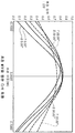
도 11은 도 1에 도시된 실시예에 대한 초점을 통한 MTF 그래프를 도시한 도면,FIG. 11 shows an MTF graph with focus for the embodiment shown in FIG. 1, FIG.
도 12는 도 2에 도시된 실시예에 대한 초점을 통한 MTF 그래프를 도시한 도면,FIG. 12 shows an MTF graph through focus for the embodiment shown in FIG. 2;
도 13은 도 3에 도시된 실시예에 대한 초점을 통한 MTF 그래프를 도시한 도면,FIG. 13 shows an MTF graph with focus for the embodiment shown in FIG. 3;
도 14는 도 4에 도시된 실시예에 대한 초점을 통한 MTF 그래프를 도시한 도 면,14 shows an MTF graph through focus for the embodiment shown in FIG. 4;
도 15는 도 5에 도시된 실시예에 대한 초점을 통한 MTF 그래프를 도시한 도면,FIG. 15 shows an MTF graph through focus for the embodiment shown in FIG. 5;
도 16은 도 6에 도시된 실시예에 대한 초점을 통한 MTF 그래프를 도시한 도면,FIG. 16 shows an MTF graph with focus for the embodiment shown in FIG. 6, FIG.
도 17은 도 7에 도시된 실시예에 대한 초점을 통한 MTF 그래프를 도시한 도면,FIG. 17 shows an MTF graph through focus for the embodiment shown in FIG. 7;
도 18은 도 8에 도시된 실시예에 대한 초점을 통한 MTF 그래프를 도시한 도면,FIG. 18 shows an MTF graph through focus for the embodiment shown in FIG. 8; FIG.
도 19는 도 9에 도시된 실시예에 대한 초점을 통한 MTF 그래프를 도시한 도면,FIG. 19 shows an MTF graph through focus for the embodiment shown in FIG. 9;
도 20은 도 10에 도시된 실시예에 대한 초점을 통한 MTF 그래프를 도시한 도면.20 shows an MTF graph through focus for the embodiment shown in FIG. 10.
본 상세한 설명은 특히 본 발명에 따른 장치의 일부를 형성하거나, 장치와 보다 직접적으로 협력하는 요소에 관한 것이다. 특별히 도시되거나 기술되지 않은 요소는 당업자에게 잘 공지된 다양한 형태일 수 있다는 것이 이해된다.The present description particularly relates to elements which form part of the device according to the invention or cooperate more directly with the device. It is understood that the elements not particularly shown or described may be in various forms well known to those skilled in the art.
본 발명의 예시적인 실시예가 도 1 내지 도 10 및 표 1 내지 표 10에 각각 도시된다. 도 1 내지 도 10 및 표 1 내지 표 10에서, 광학 시스템(10)은 광학 시스템(10)의 물체측(20)으로부터 광학 시스템(10)의 이미지측(30) 쪽으로 광학 축(15)을 따라 순서대로 배열된 3개의 렌즈 요소(E1, E2, E3)를 포함한다. 구경 조리개(40)는 렌즈 요소(E1)의 물체측 상에 위치되고, 적어도 하나의 배플(baffle)(50)은 렌즈 요소(E1, E2) 사이에 위치된다. 예컨대, 이미지 센서 또는 필름과 같은 감광성 수신기(60)는 렌즈 요소(E3)의 이미지측 상에 위치된다. 예컨대 커버 플레이트 및/또는 필터와 같은 추가적인 요소(70)는 감광성 수신기(60) 및 렌즈 요소(E3) 사이에 위치된다. 일반적인 필터는 적외선 소거 필터 및/또는 광 블러링(blurring) 필터[예컨대, 저대역 필터(low-pass filter), 대역 통과 필터(band pass filter) 등]를 포함한다. 광학 시스템(10)의 각각의 렌즈 요소(E1, E2, E3)의 표면 반경(R)은 물체측(20)에서의 시작하고 이미지측(30) 상의 종료되는 숫자가 부여된다. 표 1 내지 표 10에서, 렌즈 요소의 두께(Tn)와 렌즈 요소 사이의 공간은 양자 모두 "두께"로서 지칭되고 두께에 앞선 표면으로서 동일선 상에 기재된다. 예컨대, 표 1에서의 제 1 두께는 렌즈 요소(E1)의 두께에 상응한다. 유사하게, 표 1에서의 제 2 두께는 렌즈 요소(E1)과 배플(50) 사이의 공간에 상응한다. 표 1 내지 표 10에 제공된 모든 두께는 밀리미터 단위이다. 모든 굴절률과 [아베 수(Abbe number)로도 공지된] V 수(V-number)는 587.6nm의 파장에서 스펙트럼의 헬륨(d)선에 대한 것이다.Exemplary embodiments of the invention are shown in FIGS. 1-10 and Tables 1-10, respectively. 1-10 and Tables 1-10, the
도 1, 도 2, 표 1 및 표 2를 참조하면, 제 1 및 제 2의 예시적인 실시예가 각각 도시된다. 광학 시스템(10)은 물체측(20)으로부터 이미지측(30) 쪽으로 렌즈 요소(E1, E2, E3)를 포함한다. 렌즈 요소(E1)는 양의 굴절능과 물체측(20) 쪽으로 볼록한 요철 형상을 갖는 구형 단일체 렌즈 요소이다. 렌즈 요소(E2)는 음의 굴절능과 물체측(20) 쪽으로 오목한 요철 형상을 갖는 이중 비구면(bi-aspheric) 단일체 렌즈 요소이다. 렌즈 요소(E3)는 양의 굴절능을 갖는 구형 단일체 렌즈 요소이다.1, 2, Table 1 and Table 2, first and second exemplary embodiments are shown, respectively. The
구경 조리개(40)는 렌즈 요소(E1)의 물체측 표면상에 위치된다. 변형적으로, 구경 조리개(40)는 렌즈 요소(E1)의 물체측 표면으로부터 이격되어 위치될 수 있다. 예컨대, 광 비네팅 구경(light vignetting aperture)과 같은 배플(50)은 렌즈 요소(E1, E2) 사이에 위치된다. 변형적으로, 배플(50)은 렌즈 요소(E1, E2)의 하나 또는 양자의 표면상에 위치될 수 있다. The
렌즈 요소(E1, E2, E3)는 유리, 수지 재료(예컨대, 플라스틱) 및 수지 재료로 각각 제조된다. 그러나, 다른 재료 조합이 가능하다, 예컨대, 렌즈 요소(E1, E2, E3)는 유리, 수지 재료 및 유리로 각각 제조될 수 있다. 변형적으로, 렌즈 요소(E1, E2, E3)는 수지 재료, 수지 재료 및 유리로 각각 제조될 수 있다. 각각의 렌즈 요소(E1, E2, E3)는 수지 재료로 제조될 수 있다. 수지 재료가 사용된다면, 수지 재료는 Tg > 300℉의 유리 전이 온도를 갖는 방식일 수 있다. 또한 나노복합(nanocomposite) 광학 재료는 하나 또는 모든 렌즈 요소(E1, E2, E3)에서 사용될 수 있다.The lens elements E 1 , E 2 , E 3 are each made of glass, resin material (eg plastic) and resin material. However, other material combinations are possible, for example the lens elements E 1 , E 2 , E 3 can be made of glass, resin material and glass, respectively. Alternatively, the lens elements E 1 , E 2 , E 3 can be made of resin material, resin material and glass, respectively. Each lens element E 1 , E 2 , E 3 can be made of a resin material. If a resinous material is used, the resinous material is T g And a glass transition temperature of> 300 ° F. Nanocomposite optical materials can also be used in one or all lens elements E 1 , E 2 , E 3 .
도 1, 도 2, 표 1 및 표 2에 각각 기술된 광학 시스템(10)은 적어도 25°의 물체 공간 내에 반 시야(half field of view)와, f/4 미만의 상대 구경 및 1.60 미만의 최대 굴절률을 갖는다. 추가적으로, 광학 시스템(10)은 L/f0 < 1.25 조건을 만족시키는데, L은 최말단 꼭지점으로부터 이미지 평면 쪽으로의 전체 시스템 길이이고, f0는 렌즈의 유효 초점 거리이다.The
렌즈 요소(E1, E2 및/또는 E3)는 매우 낮은 분산 재료(예컨대, 아베 수 Vd > 65인 재료)로 제조될 수 있다. 예컨대, 도 2 및 표 2에 도시된 예시적인 실시예에서, 렌즈 요소(E1)는 구형이고, 매우 낮은 분산 재료(아베 수 Vd > 65인 재료, 보다 바람직하게는 아베 수 Vd > 80인 재료)로 제조될 수 있다. 도 1 및 표 1에 도시된 실시예와 유사하지만, 렌즈 요소(E1)에 대한 매우 낮은 분산 재료의 사용은 광학 시스템(10)의 다색(polychromatic) 성능을 개선시킨다.The lens elements E 1 , E 2 and / or E 3 can be made of very low dispersion materials (eg materials with Abbe numbers V d > 65). For example, in the exemplary embodiment shown in FIGS. 2 and 2, the lens element E 1 is spherical and has a very low dispersion material (a material having an Abbe number V d > 65, more preferably an Abbe number V d > 80). Phosphorus material). Although similar to the embodiment shown in FIG. 1 and Table 1, the use of a very low dispersion material for lens element E 1 improves the polychromatic performance of
도 3 및 표 3을 참조하면, 제 3의 예시적인 실시예가 도시된다. 광학 시스템(10)은 물체측(20)으로부터 이미지측(30) 쪽으로 렌즈 요소(E1, E2, E3)를 포함한다. 렌즈 요소(E1)는 양의 굴절능과 물체측(20) 쪽으로 볼록한 요철 형상을 갖는 이중 비구면 단일체 렌즈 요소이다. 렌즈 요소(E2)는 음의 굴절능과 물체측(20) 쪽으로 오목한 요철 형상을 갖는 구형 단일체 렌즈 요소이다. 렌즈 요소(E3)는 양의 굴절능을 갖는 이중 비구면 단일체 렌즈 요소이다. 3 and Table 3, a third exemplary embodiment is shown. The
구경 조리개(40)는 렌즈 요소(E1)의 물체측 표면상에 위치된다. 변형적으로, 구경 조리개(40)는 렌즈 요소(E1)의 물체측 표면으로부터 이격되어 위치될 수 있다. 예컨대, 광 비네팅 구경과 같은 배플(50)은 렌즈 요소(E1, E2) 사이에 위치된다. 변형적으로, 배플(50)은 렌즈 요소(E1, E2)의 하나 또는 양자의 표면상에 위치될 수 있다. The
렌즈 요소(E1, E2, E3)는 수지 재료(예컨대, 플라스틱), 수지 재료 및 수지 재료로 각각 제조될 수 있다. 그러나, 다른 재료 조합이 가능하다. 예컨대, 렌즈 요소(E1, E2, E3)는 수지 재료, 유리 및 수지 재료로 각각 제조될 수 있다. 수지 재료가 사용된다면, 수지 재료는 Tg > 300℉의 유리 전이 온도를 갖는 방식일 수 있다. 또한 나노복합 광학 재료는 하나 또는 모든 렌즈 요소(E1, E2, E3)에서 사용될 수 있다. 변형적으로, 렌즈 요소(E1, E2 및/또는 E3)는 매우 낮은 분산 재료(예컨대, 아베 수 Vd > 65인 재료)로 제조될 수 있다. The lens elements E 1 , E 2 , E 3 can each be made of a resin material (eg plastic), a resin material and a resin material. However, other material combinations are possible. For example, lens elements E 1 , E 2 , E 3 can be made of resin material, glass and resin material, respectively. If a resinous material is used, the resinous material is T g And a glass transition temperature of> 300 ° F. Nanocomposite optical materials can also be used in one or all lens elements E 1 , E 2 , E 3 . Alternatively, the lens elements E 1 , E 2 and / or E 3 can be made of very low dispersion materials (eg materials with Abbe numbers V d > 65).
도 3 및 표 3에 각각 기술된 광학 시스템(10)은 적어도 25°의 물체 공간 내에 반 시야와, f/4 미만의 상대 구경 및 1.60 미만의 최대 굴절률을 갖는다. 추가적으로, 광학 시스템(10)은 L/f0 < 1.25 조건을 만족시키는데, L은 최말단 꼭지점으로부터 이미지 평면 쪽으로의 전체 시스템 길이이고, f0는 렌즈의 유효 초점 거리이다.The
도 4, 도 5, 표 4 및 표 5를 참조하면, 제 4 및 제 5의 예시적인 실시예가 각각 도시된다. 광학 시스템(10)은 물체측(20)으로부터 이미지측(30) 쪽으로 렌즈 요소(E1, E2, E3)를 포함한다. 렌즈 요소(E1)는 양의 굴절능과 물체측(20) 쪽으로 볼록한 요철 형상을 갖는 이중 비구면 단일체 렌즈 요소이다. 렌즈 요소(E2)는 음의 굴절능과 물체측(20) 쪽으로 오목한 요철 형상을 갖는 이중 비구면 단일체 렌즈 요소이다. 렌즈 요소(E3)는 양의 굴절능을 갖는 구형 단일체 렌즈 요소이다. 4, 5, Table 4 and Table 5, fourth and fifth exemplary embodiments are shown, respectively. The
구경 조리개(40)는 렌즈 요소(E1)의 물체측 표면상에 위치된다. 변형적으로, 구경 조리개(40)는 렌즈 요소(E1)의 물체측 표면으로부터 이격되어 위치될 수 있다. 예컨대, 광 비네팅 구경과 같은 배플(50)은 렌즈 요소(E1, E2) 사이에 위치된다. 변형적으로, 배플(50)은 렌즈 요소(E1, E2)의 하나 또는 양자의 표면상에 위치될 수 있다. The
렌즈 요소(E1, E2, E3)는 수지 재료(예컨대, 플라스틱), 수지 재료 및 수지 재료로 각각 제조될 수 있다. 그러나, 다른 재료 조합이 가능하다. 예컨대, 렌즈 요소(E1, E2, E3)는 수지 재료, 수지 재료 및 유리로 각각 제조될 수 있다. 또한 나노복합 광학 재료는 하나 또는 모든 렌즈 요소(E1, E2, E3)에서 사용될 수 있다. 변형적으로, 렌즈 요소(E1, E2 및/또는 E3)는 매우 낮은 분산 재료(예컨대, 아베 수 Vd > 65인 재료)로 제조될 수 있다. The lens elements E 1 , E 2 , E 3 can each be made of a resin material (eg plastic), a resin material and a resin material. However, other material combinations are possible. For example, lens elements E 1 , E 2 , E 3 can be made of resin material, resin material and glass, respectively. Nanocomposite optical materials can also be used in one or all lens elements E 1 , E 2 , E 3 . Alternatively, the lens elements E 1 , E 2 and / or E 3 can be made of very low dispersion materials (eg materials with Abbe numbers V d > 65).
도 4, 도 5, 표 4 및 표 5에 각각 기술된 광학 시스템(10)은 적어도 25°의 물체 공간 내에 반 시야와, f/4 미만의 상대 구경 및 1.60 미만의 최대 굴절률을 갖는다. 추가적으로, 광학 시스템(10)은 L/f0 < 1.25 조건을 만족시키는데, L은 최말단 꼭지점으로부터 이미지 평면 쪽으로의 전체 시스템 길이이고, f0는 렌즈의 유효 초점 거리이다.The
수지 재료가 사용된다면, 수지 재료는 Tg > 300℉의 유리 전이 온도를 갖는 방식일 수 있다. 예컨대, 도 5 및 표 5에 도시된 예시적인 실시예에서, 모든 3개의 렌즈 요소(E1, E2, E3)는 고온 조립체의 작동, 저장 및 사용을 허용하기 위해, Tg > 300℉의 유리 전이 온도를 갖는 방식의 수지 재료로 제조될 수 있다.If a resinous material is used, the resinous material is T g And a glass transition temperature of> 300 ° F. For example, in the exemplary embodiment shown in FIG. 5 and Table 5, all three lens elements E 1 , E 2 , E 3 have a T g > 300 ° F. to allow operation, storage and use of the high temperature assembly. It can be made of a resin material in a manner having a glass transition temperature of.
도 6 내지 도 8 및 표 6 내지 표 8을 참조하면, 제 6 내지 제 8의 예시적인 실시예가 각각 도시된다. 광학 시스템(10)은 물체측(20)으로부터 이미지측(30) 쪽으로 렌즈 요소(E1, E2, E3)를 포함한다. 렌즈 요소(E1)는 양의 굴절능과 물체측(20) 쪽으로 볼록한 요철 형상을 갖는 비구면 단일체 렌즈 요소이다. 렌즈 요소(E1)의 한쪽 또는 양쪽 표면은 비구면일 수 있다. 렌즈 요소(E2)는 음의 굴절능과 물체측(20) 쪽으로 오목한 요철 형상을 갖는 비구면 단일체 렌즈 요소이다. 렌즈 요소(E2)의 한쪽 또는 양쪽 표면은 비구면일 수 있다. 렌즈 요소(E3)는 양의 굴절능을 갖는 비구면 단일체 렌즈 요소이다. 렌즈 요소(E3)의 한쪽 또는 양쪽 표면은 비구면일 수 있다.6-8 and Tables 6-8, sixth and eighth exemplary embodiments are shown, respectively. The
구경 조리개(40)는 렌즈 요소(E1)의 물체측 표면상에 위치된다. 변형적으로, 구경 조리개(40)는 렌즈 요소(E1)의 물체측 표면으로부터 이격되어 위치될 수 있다. 예컨대, 광 비네팅 구경과 같은 배플(50)은 렌즈 요소(E1, E2) 사이에 위치된다. 변형적으로, 배플(50)은 렌즈 요소(E1, E2)의 하나 또는 양자의 표면상에 위치될 수 있다. The
렌즈 요소(E1, E2, E3)는 수지 재료(예컨대, 플라스틱)로 각각 제조될 수 있다. 수지 재료가 사용된다면, 수지 재료는 Tg > 300℉의 유리 전이 온도를 갖는 방식일 수 있다. 또한 나노복합 광학 재료는 하나 또는 모든 렌즈 요소(E1, E2, E3)에서 사용될 수 있다. 변형적으로, 렌즈 요소(E1, E2 및/또는 E3)는 매우 낮은 분산 재료(예컨대, 아베 수 Vd > 65인 재료)로 제조될 수 있다. The lens elements E 1 , E 2 , E 3 can each be made of a resin material (eg plastic). If a resinous material is used, the resinous material is T g And a glass transition temperature of> 300 ° F. Nanocomposite optical materials can also be used in one or all lens elements E 1 , E 2 , E 3 . Alternatively, the lens elements E 1 , E 2 and / or E 3 can be made of very low dispersion materials (eg materials with Abbe numbers V d > 65).
도 6 내지 도 8 및 표 6 내지 표 8에 각각 기술된 광학 시스템(10)은 적어도 25°의 물체 공간 내에 반 시야와, f/4 미만의 상대 구경 및 1.60 미만의 최대 굴절률을 갖는다. 추가적으로, 광학 시스템(10)은 L/f0 < 1.25 조건을 만족시키는데, L은 최말단 꼭지점으로부터 이미지 평면 쪽으로의 전체 시스템 길이이고, f0는 렌즈의 유효 초점 거리이다.The
도 1 내지 도 8 및 표 1 내지 표 8을 각각 참조하면, 광학 시스템(10)의 각각의 예시적인 실시예는 렌즈 요소(E1)의 물체측 표면으로부터 감광성 수신기(60) 쪽으로의 전체 시스템 길이(L)는 약 6mm이고, 각각의 이러한 예시적인 경우의 유효 초점 거리(f0)는 약 5mm이며, 1.20 미만인 L/f0의 비율이 주어진다. 각각의 예시적인 실시예는 적어도 28°의 준 시야(semi-field of view)를 포함하고, F/2.8이거나 보다 고속 촬영용이며, 이미지의 중심부에서 조명이 대략 50%(또는 그 이상)인 코너부에 상대적인 조명을 가지며, 4% 미만 크기의 최대 왜곡(distortion)을 가지며, 감광성 수신기(10) 또는 센서 평면에서 최대 주 광선 각도를 수직인 센서 평면에 비해 약 20°미만이 되도록 제한한다.1-8 and Tables 1-8, respectively, each exemplary embodiment of the
도 9 및 표 9를 참조하면, 제 9의 예시적인 실시예가 도시된다. 광학 시스템(10)은 물체측(20)으로부터 이미지측(30) 쪽으로 렌즈 요소(E1, E2, E3)를 포함한다. 렌즈 요소(E1)는 양의 굴절능과 물체측(20) 쪽으로 볼록한 요철 형상을 갖는 비구면 단일체 렌즈 요소이다. 이러한 실시예에서, 렌즈 요소(E1)의 이미지측 표면은 비구면이지만, 렌즈 요소(E1)의 한쪽 표면이 비구면일 수 있다. 렌즈 요소(E2)는 음의 굴절능과 물체측(20) 쪽으로 오목한 요철 형상을 갖는 이중 비구면 단일체 렌즈 요소이다. 렌즈 요소(E3)는 양의 굴절능을 갖는 비구면 단일체 렌즈 요소이다. 이러한 실시예에서, 렌즈 요소(E3)의 이미지측 표면은 비구면이지만, 렌즈 요소(E3)의 한쪽 표면이 비구면일 수 있다.9 and Table 9, a ninth exemplary embodiment is shown. The
구경 조리개(40)는 렌즈 요소(E1)의 물체측 표면으로부터 이격되어 위치된다. 변형적으로, 구경 조리개(40)는 렌즈 요소(E1)의 물체측 표면상에 위치될 수 있다. 예컨대, 광 비네팅 구경과 같은 배플(50)은 렌즈 요소(E1, E2) 사이에 위치된다. 변형적으로, 배플(50)은 렌즈 요소(E1, E2)의 하나 또는 양자의 표면상에 위치될 수 있다. 예컨대, 광 비네팅 구경 및/또는 글레어(glare) 구경과 같은 다른 배플(50)은 렌즈 요소(E2)의 이미지측 표면상에 위치된다. 변형적으로, 이러한 배플(50)(들)은 렌즈 요소(E2, E3) 사이 또는 렌즈 요소(E3)의 표면상에 위치될 수 있다. The
렌즈 요소(E1, E2, E3)는 수지 재료(예컨대, 플라스틱)로 각각 제조될 수 있다. 수지 재료가 사용된다면, 수지 재료는 Tg > 300℉의 유리 전이 온도를 갖는 방식일 수 있다. 또한 나노복합 광학 재료는 하나 또는 모든 렌즈 요소(E1, E2, E3)에서 사용될 수 있다. 변형적으로, 렌즈 요소(E1, E2 및/또는 E3)는 매우 낮은 분산 재료(예컨대, 아베 수 Vd > 65인 재료)로 제조될 수 있다. The lens elements E 1 , E 2 , E 3 can each be made of a resin material (eg plastic). If a resinous material is used, the resinous material is T g And a glass transition temperature of> 300 ° F. Nanocomposite optical materials can also be used in one or all lens elements E 1 , E 2 , E 3 . Alternatively, the lens elements E 1 , E 2 and / or E 3 can be made of very low dispersion materials (eg materials with Abbe numbers V d > 65).
도 9 및 표 9에 기술된 광학 시스템(10)은 적어도 25°의 물체 공간 내에 반 시야와, f/4 미만의 상대 구경 및 1.60 미만의 최대 굴절률을 갖는다. 추가적으로, 광학 시스템(10)은 L/f0 < 1.25 조건을 만족시키는데, L은 최말단 꼭지점으로부터 이미지 평면 쪽으로의 전체 시스템 길이이고, f0는 렌즈의 유효 초점 거리이다. 광학 시스템(10)은 구경 조리개(40)로부터 감광성 수신기(60) 쪽으로 약 6.3mm인 전체 시스템 길이(L)와, 약 5.3mm인 유효 초점 거리(f0)와, 1.20 미만인 L/f0의 비율을 갖는다. 이러한 예시적인 실시예는 적어도 29°의 준 시야를 포함하고, F/2.8이거나 보다 고속 촬영용이며, 이미지의 중심부에서 조명이 대략 50%(또는 그 이상)인 코너부에 상대적인 조명을 가지며, 4% 미만 크기의 최대 왜곡을 가지며, 감광성 수신기(10) 또는 센서 평면에서 최대 주 광선 각도를 수직인 센서 평면에 비해 약 22°미만이 되도록 제한한다.The
도 10 및 표 10을 참조하면, 제 10의 예시적인 실시예가 도시된다. 광학 시스템(10)은 물체측(20)으로부터 이미지측(30) 쪽으로 렌즈 요소(E1, E2, E3)를 포함한다. 렌즈 요소(E1)는 양의 굴절능과 물체측(20) 쪽으로 볼록한 요철 형상을 갖는 비구면 단일체 렌즈 요소이다. 이러한 실시예에서, 렌즈 요소(E1)의 이미지측 표면은 비구면이지만, 렌즈 요소(E1)의 한쪽 표면이 비구면일 수 있다. 렌즈 요소(E2)는 음의 굴절능과 물체측(20) 쪽으로 오목한 요철 형상을 갖는 이중 비구면 단일체 렌즈 요소이다. 렌즈 요소(E3)는 양의 굴절능을 갖는 비구면 단일체 렌즈 요소이다. 이러한 실시예에서, 렌즈 요소(E3)의 이미지측 표면은 비구면이지만, 렌즈 요소(E3)의 한쪽 표면이 비구면일 수 있다.10 and Table 10, a tenth exemplary embodiment is shown. The
구경 조리개(40)는 렌즈 요소(E1)의 물체측 표면으로부터 이격되어 위치된다. 변형적으로, 구경 조리개(40)는 렌즈 요소(E1)의 물체측 표면상에 위치될 수 있다. 예컨대, 광 비네팅 구경과 같은 배플(50)은 렌즈 요소(E1, E2) 사이에 위치된다. 변형적으로, 배플(50)은 렌즈 요소(E1, E2)의 하나 또는 양자의 표면상에 위치될 수 있다. 예컨대, 광 비네팅 구경 및/또는 섬광 구경과 같은 다른 배플(50)은 렌즈 요소(E2)의 이미지측 표면상에 위치된다. 변형적으로, 이러한 배플(50)(들)은 렌즈 요소(E2, E3) 사이 또는 렌즈 요소(E3)의 표면상에 위치될 수 있다. The
렌즈 요소(E1, E2, E3)는 수지 재료(예컨대, 플라스틱)로 각각 제조될 수 있다. 수지 재료가 사용된다면, 수지 재료는 Tg > 300℉의 유리 전이 온도를 갖는 방식일 수 있다. 또한 나노복합 광학 재료는 하나 또는 모든 렌즈 요소(E1, E2, E3)에서 사용될 수 있다. 변형적으로, 렌즈 요소(E1, E2 및/또는 E3)는 매우 낮은 분산 재료(예컨대, 아베 수 Vd > 65인 재료)로 제조될 수 있다. The lens elements E 1 , E 2 , E 3 can each be made of a resin material (eg plastic). If a resinous material is used, the resinous material is T g And a glass transition temperature of> 300 ° F. Nanocomposite optical materials can also be used in one or all lens elements E 1 , E 2 , E 3 . Alternatively, the lens elements E 1 , E 2 and / or E 3 can be made of very low dispersion materials (eg materials with Abbe numbers V d > 65).
도 10 및 표 10에 기술된 광학 시스템(10)은 적어도 25°의 물체 공간 내에 반 시야와, f/4 미만의 상대 구경 및 1.60 미만의 최대 굴절률을 갖는다. 추가적으로, 광학 시스템(10)은 L/f0 < 1.25 조건을 만족시키는데, L은 최말단 꼭지점으로부터 이미지 평면 쪽으로의 전체 시스템 길이이고, f0는 렌즈의 유효 초점 거리이다. 광학 시스템(10)은 구경 조리개(40)로부터 감광성 수신기(60) 쪽으로 약 7.13mm인 전체 시스템 길이(L)와, 약 6.0mm인 유효 초점 거리(f0)와, 1.20 미만인 L/f0의 비율을 갖는다. 이러한 예시적인 실시예는 적어도 30°의 준 시야를 포함하고, F/2.8이거나 보다 고속 촬영용이며, 이미지의 중심부에서 조명이 대략 50%(또는 그 이상)인 코너부에 상대적인 조명을 가지며, 4% 미만 크기의 최대 왜곡을 가지며, 감광성 수신기(10) 또는 센서 평면에서 최대 주 광선 각도를 수직인 센서 평면에 비해 약 22°미만이 되도록 제한한다.The
도 1 내지 도 10 및 표 1 내지 표 10을 각각 참조하면, 예시적인 실시예에 기술된 각각의 구형 렌즈 요소는 낮은 굴절률의 재료(Nd < 1.6)로 제조된다. 이와 같이, 각각의 구형 요소는 하나의 광학 유리로 제조될 수 있거나, 매우 작은 곡선만 갖는 수지 재료는 이러한 요소를 변경시키는 한편, 광학 시스템(10)의 다른 렌즈 요소는 (필요하다면) 고정되어 유지된다. 이것은 예컨대, 2개의 유리 구형 렌즈 요소 및 하나의 플라스틱 렌즈 요소를 구비하여 광학 시스템(10)의 원형(prototype)이 만들어지도록 한다. 그 후에, 생산시에, 2개의 유리 구형 렌즈 요소는 다른 광학 요소(들)로의 변형이 없고, 장착 하드웨어[배럴(barrel), 스페이서(spacer) 등]로의 변형이 적거나 없는 구형 플라스틱 요소로 대체될 수 있다.1 to 10 and Tables 1 to 10, respectively, each of the spherical lens elements described in the exemplary embodiment is a low refractive index material (N d). <1.6). As such, each spherical element may be made of one optical glass, or a resin material having only a very small curve changes this element, while the other lens elements of the
이러한 방식으로, 제조자는 최소의 추가 비용을 위해, 필요하다면, 제품 수명의 임의의 시점에서 광학 유리 요소 또는 플라스틱 수지 요소 중 하나의 특이한 이점을 사용하는 광학 시스템(10)의 실시예 사이에서 전환할 수 있다. 통상적으로, 유리에 있어서의 주요 이점은 ① 보다 열적으로 안정한 설계, ② 보다 적은 비용의 원형, ③ 보다 신속한 생산 원형이다. 플라스틱 수지에 있어서의 주요 이점은 ① 보다 적은 비용의 큰 용적 제품 설계, ② 보다 가벼운 중량 설계이다.In this way, manufacturers can switch between embodiments of the
광학 시스템(10)의 구형 표면(들)을 갖는 렌즈 요소(E1, E2 및/또는 E3)는 일반적으로 수지 재료로 제조된다. 변형적으로, 이러한 요소는 유리로 제조될 수 있지만, 비용 문제점은 이것을 불가능하게 할 수 있다. 광학 시스템(10)의 구형 표면(들)을 갖는 렌즈 요소(E1, E2 및/또는 E3)는 필요하다면, 낮은 굴절률의 유리 또는 수지 재료 중 하나로 제조될 수 있다.Lens elements E 1 , E 2 and / or E 3 having spherical surface (s) of
적절한 감광성 수신기(60)는 예컨대, 변형 결합된 장치(CCD)와 상보성 금속 산화막 센서(complementary metal-oxide sensor;CMOS)를 포함한다. 추가적으로, 상술된 광학 시스템(10)은 약 8mm 미만인 능동적 대각 치수(active diagonal dimension)를 갖는 이러한 방식의 감광성 수신기(센서)와 함께 기능한다. 변형적으로, 상술된 광학 시스템(10)은 확대되거나 축소될 수 있어서, 보다 크거나 작은 능동적 대각 치수를 갖는 감광성 수신기(센서)를 구비하여 기능한다.Suitable
상술된 광학 시스템(10)은 다양한 필름 및/또는 전자 이미지 적용을 자체에 추가한다. 특히, 광학 시스템(10)은 소비자 모바일 이미지 적용, 예컨대, 카메라 사용 가능 핸드폰 및 개인 휴대용 정보 단말기(PDA)에서 적절하게 사용된다. The
도 11 내지 도 20에 도시된 초점을 통한 MTF 그래프는 도 1 내지 도 10 및 표 1 내지 표 10에 기술된 실시예에 대해 각각 다색성(0.35에서 486nm, 1.00에서 538nm 및 0.50에서 597nm)이다. MTF 그래프는 밀리미터당 33 라인 쌍으로 도시된다.The MTF graphs through focus shown in FIGS. 11-20 are polychromatic (486 nm at 0.35, 538 nm at 1.00 and 597 nm at 0.50) for the embodiments described in FIGS. 1-10 and Tables 1-10, respectively. MTF graphs are shown as 33 line pairs per millimeter.
본 발명은 임의의 바람직한 실시예에 대해 특정한 참고로 상세하게 기술되었지만, 변형 및 수정이 발명의 범위 내에서 달성될 수 있다.Although the present invention has been described in detail with reference to certain preferred embodiments, variations and modifications can be made within the scope of the invention.
< 표 1 ><Table 1>

< 표 2 ><Table 2>

< 표 3 ><Table 3>

< 표 4 ><Table 4>

< 표 5 ><Table 5>

< 표 6 ><Table 6>

< 표 7><Table 7>

< 표 8 ><Table 8>

< 표 9 ><Table 9>

< 표 10 ><Table 10>

Claims (28)
Applications Claiming Priority (4)
| Application Number | Priority Date | Filing Date | Title |
|---|---|---|---|
| US51724203P | 2003-11-04 | 2003-11-04 | |
| US60/517,242 | 2003-11-04 | ||
| US10/974,630 | 2004-10-27 | ||
| US10/974,630 US7061695B2 (en) | 2003-11-04 | 2004-10-27 | Three element optical system |
Publications (1)
| Publication Number | Publication Date |
|---|---|
| KR20060107762A true KR20060107762A (en) | 2006-10-16 |
Family
ID=34556276
Family Applications (1)
| Application Number | Title | Priority Date | Filing Date |
|---|---|---|---|
| KR1020067008651A KR20060107762A (en) | 2003-11-04 | 2004-11-03 | Objective lens system having three lenses |
Country Status (5)
| Country | Link |
|---|---|
| US (1) | US7061695B2 (en) |
| JP (1) | JP2007510955A (en) |
| KR (1) | KR20060107762A (en) |
| TW (1) | TW200530653A (en) |
| WO (1) | WO2005045500A1 (en) |
Cited By (1)
| Publication number | Priority date | Publication date | Assignee | Title |
|---|---|---|---|---|
| KR101527990B1 (en) * | 2007-11-07 | 2015-06-10 | 난창 오-필름 옵토일렉트로닉스 테크놀로지 리미티드 | Customized depth of field optical system and compact fast lens architecture |
Families Citing this family (30)
| Publication number | Priority date | Publication date | Assignee | Title |
|---|---|---|---|---|
| JP3770493B2 (en) * | 2003-06-24 | 2006-04-26 | フジノン株式会社 | Imaging lens |
| JP4567366B2 (en) * | 2004-04-23 | 2010-10-20 | 株式会社エンプラス | Imaging lens |
| EP1653267B1 (en) * | 2004-11-01 | 2007-12-19 | Konica Minolta Opto, Inc. | Compact imaging lens having three single lenses |
| TWI255361B (en) * | 2005-05-05 | 2006-05-21 | Largan Precision Co Ltd | Optical imaging lens array |
| JP2007086485A (en) * | 2005-09-22 | 2007-04-05 | Fujinon Corp | Imaging lens |
| JP4804856B2 (en) * | 2005-09-29 | 2011-11-02 | 富士フイルム株式会社 | Single focus lens |
| JP4804858B2 (en) * | 2005-09-29 | 2011-11-02 | 富士フイルム株式会社 | Single focus lens |
| JP4804857B2 (en) * | 2005-09-29 | 2011-11-02 | 富士フイルム株式会社 | Single focus lens |
| US20070091469A1 (en) * | 2005-10-19 | 2007-04-26 | Genius Electronic Optical Co. Ltd. | Image-forming lens set |
| JP2008139786A (en) * | 2006-12-05 | 2008-06-19 | Largan Precision Co Ltd | Photographic lens |
| JP2008203822A (en) * | 2007-01-24 | 2008-09-04 | Konica Minolta Opto Inc | Image pickup lens, image pickup apparatus and mobile terminal |
| JP2008225332A (en) * | 2007-03-15 | 2008-09-25 | Sony Corp | Imaging lens |
| JP2009053411A (en) * | 2007-08-27 | 2009-03-12 | Hoya Corp | Image reading lens system |
| US20100295973A1 (en) * | 2007-11-06 | 2010-11-25 | Tessera North America, Inc. | Determinate and indeterminate optical systems |
| JP2009222950A (en) * | 2008-03-16 | 2009-10-01 | E-Pin Optical Industry Co Ltd | Imaging lens |
| CN101963693B (en) * | 2009-07-22 | 2012-06-20 | 比亚迪股份有限公司 | Optical lens assembly |
| CN101846793A (en) * | 2010-05-28 | 2010-09-29 | 浙江舜宇光学有限公司 | Micro pickup lens |
| JP2015060067A (en) | 2013-09-18 | 2015-03-30 | 株式会社東芝 | Imaging lens and solid-state imaging device |
| RU2593413C2 (en) * | 2014-08-22 | 2016-08-10 | Открытое акционерное общество "Корпорация космических систем специального назначения "Комета" | High-aperture lens |
| TWI561850B (en) * | 2015-05-15 | 2016-12-11 | Ability Opto Electronics Technology Co Ltd | Optical image capturing system |
| US10007115B2 (en) | 2015-08-12 | 2018-06-26 | Daqri, Llc | Placement of a computer generated display with focal plane at finite distance using optical devices and a see-through head-mounted display incorporating the same |
| US10649209B2 (en) | 2016-07-08 | 2020-05-12 | Daqri Llc | Optical combiner apparatus |
| CN106094178B (en) * | 2016-07-18 | 2019-03-22 | 瑞声科技(新加坡)有限公司 | Pick-up lens |
| US10481678B2 (en) | 2017-01-11 | 2019-11-19 | Daqri Llc | Interface-based modeling and design of three dimensional spaces using two dimensional representations |
| US10488666B2 (en) | 2018-02-10 | 2019-11-26 | Daqri, Llc | Optical waveguide devices, methods and systems incorporating same |
| US11125993B2 (en) | 2018-12-10 | 2021-09-21 | Facebook Technologies, Llc | Optical hyperfocal reflective systems and methods, and augmented reality and/or virtual reality displays incorporating same |
| JP2022514489A (en) | 2018-12-10 | 2022-02-14 | フェイスブック・テクノロジーズ・リミテッド・ライアビリティ・カンパニー | Adaptive viewport for hypervocal viewport (HVP) displays |
| KR20210111278A (en) | 2019-01-09 | 2021-09-10 | 페이스북 테크놀로지스, 엘엘씨 | Non-uniform sub-pupil reflectors and methods of optical waveguides for AR, HMD and HUD applications |
| TWI827857B (en) * | 2020-07-03 | 2024-01-01 | 先進光電科技股份有限公司 | Optical image capturing system |
| US11863730B2 (en) | 2021-12-07 | 2024-01-02 | Snap Inc. | Optical waveguide combiner systems and methods |
Family Cites Families (29)
| Publication number | Priority date | Publication date | Assignee | Title |
|---|---|---|---|---|
| US3910685A (en) * | 1974-11-05 | 1975-10-07 | Eastman Kodak Co | Three element objective lens with aspheres on rear surfaces of first and second elements |
| JPS6091318A (en) * | 1983-10-26 | 1985-05-22 | Nitto Kogaku Kk | Objective lens for optical disk |
| JPS6177816A (en) * | 1984-09-26 | 1986-04-21 | Ricoh Co Ltd | Front stop wide angle lens |
| JPS6275609A (en) * | 1985-09-30 | 1987-04-07 | Minolta Camera Co Ltd | Projection lens for microfilm |
| JPS6340116A (en) * | 1986-08-05 | 1988-02-20 | Minolta Camera Co Ltd | Projection lens for microfilm |
| JPH01162314U (en) * | 1988-04-28 | 1989-11-13 | ||
| JP2900435B2 (en) * | 1989-10-13 | 1999-06-02 | ミノルタ株式会社 | Compact zoom lens |
| US5251069A (en) * | 1989-12-28 | 1993-10-05 | Asahi Kogaku Kogyo K.K. | Imaging lens system |
| JP3032909B2 (en) * | 1991-02-18 | 2000-04-17 | オリンパス光学工業株式会社 | Bright single focus lens |
| US5572369A (en) * | 1993-06-29 | 1996-11-05 | Eastman Kodak Company | Triplet-type lens for use in a compact photographic camera |
| US5677798A (en) * | 1993-10-28 | 1997-10-14 | Asahi Kogaku Kogyo Kabushiki Kaisha | Image forming lens system |
| JP2848523B2 (en) * | 1996-09-27 | 1999-01-20 | 株式会社日出 | Imaging lens |
| DE69735215T2 (en) * | 1996-11-29 | 2006-08-24 | 3M Innovative Properties Co., St. Paul | Lenses for an electronic imaging system |
| US5999334A (en) * | 1997-01-14 | 1999-12-07 | Minolta Co., Ltd. | Fixed focal length lens system |
| JP4173210B2 (en) * | 1997-04-30 | 2008-10-29 | フジノン株式会社 | Imaging lens |
| JPH1123959A (en) * | 1997-07-08 | 1999-01-29 | Canon Inc | Photographing lens |
| EP1164786B1 (en) * | 1997-07-30 | 2004-10-27 | Pinotage, LLC | Imaging device |
| KR20010071407A (en) * | 1998-06-05 | 2001-07-28 | 엘리스 아이. 베텐스키 | Inverse triplet lens assemblies |
| JP3767182B2 (en) * | 1998-07-17 | 2006-04-19 | ソニー株式会社 | Imaging lens and lens system |
| US6282033B1 (en) * | 1999-09-07 | 2001-08-28 | Alex Ning | Lens with external aperture stop |
| US6441971B2 (en) * | 1999-09-27 | 2002-08-27 | Alex Ning | Compact lens with external aperture stop |
| JP3478265B2 (en) * | 2000-06-12 | 2003-12-15 | ミノルタ株式会社 | Imaging lens device |
| JP2002162561A (en) | 2000-11-27 | 2002-06-07 | Casio Comput Co Ltd | Photographic lens |
| JP3424030B2 (en) * | 2001-01-31 | 2003-07-07 | カシオ計算機株式会社 | Shooting lens |
| US6577456B2 (en) * | 2001-03-29 | 2003-06-10 | Fuji Photo Optical Co., Ltd. | Single focus lens |
| JP2003005031A (en) * | 2001-06-18 | 2003-01-08 | Milestone Kk | Lens for image pick-up |
| JP4312596B2 (en) * | 2001-07-20 | 2009-08-12 | ミシェル・サヤグ | Lens system optically coupled to an image capture device |
| ATE315794T1 (en) * | 2002-03-25 | 2006-02-15 | Konishiroku Photo Ind | THREE LENS LENS |
| US6927925B2 (en) * | 2003-03-12 | 2005-08-09 | Olympus Corporation | Imaging optical system |
-
2004
- 2004-10-27 US US10/974,630 patent/US7061695B2/en not_active Expired - Fee Related
- 2004-11-03 KR KR1020067008651A patent/KR20060107762A/en not_active Application Discontinuation
- 2004-11-03 JP JP2006538502A patent/JP2007510955A/en active Pending
- 2004-11-03 TW TW093133502A patent/TW200530653A/en unknown
- 2004-11-03 WO PCT/US2004/036908 patent/WO2005045500A1/en active Application Filing
Cited By (1)
| Publication number | Priority date | Publication date | Assignee | Title |
|---|---|---|---|---|
| KR101527990B1 (en) * | 2007-11-07 | 2015-06-10 | 난창 오-필름 옵토일렉트로닉스 테크놀로지 리미티드 | Customized depth of field optical system and compact fast lens architecture |
Also Published As
| Publication number | Publication date |
|---|---|
| JP2007510955A (en) | 2007-04-26 |
| US7061695B2 (en) | 2006-06-13 |
| US20050094292A1 (en) | 2005-05-05 |
| WO2005045500A1 (en) | 2005-05-19 |
| TW200530653A (en) | 2005-09-16 |
Similar Documents
| Publication | Publication Date | Title |
|---|---|---|
| KR20060107762A (en) | Objective lens system having three lenses | |
| US11733490B2 (en) | Optical system | |
| US6377404B1 (en) | Reverse telephoto zoom lens | |
| US10481365B2 (en) | Optical system | |
| US9910248B2 (en) | Lens module | |
| US9195029B2 (en) | Optical system | |
| US7684127B2 (en) | Imaging lens and imaging device | |
| US20170102522A1 (en) | Optical imaging system | |
| US8027099B2 (en) | Optical system for camera | |
| CN110412720B (en) | Optical lens | |
| KR100921146B1 (en) | Lens Module | |
| CN113985589A (en) | Zoom lens and optical system | |
| CN111198430B (en) | Optical lens and imaging apparatus | |
| KR20160059239A (en) | Photographic Lens Optical System | |
| KR20120094730A (en) | Photographic lens optical system | |
| US20220413266A1 (en) | Imaging optical system and device | |
| EP3474057A1 (en) | Image-capturing optical system and image-capturing device | |
| CN201083875Y (en) | Micro-optical lens | |
| CN111025601B (en) | Wide-angle large-aperture athermal day and night lens and using method thereof | |
| CN111007658B (en) | Low-cost athermal day and night lens and working method thereof | |
| JP5006627B2 (en) | Optical system and optical apparatus having the same | |
| CN100430771C (en) | Objective lens system having three lenses | |
| CN114859504B (en) | Optical lens and electronic device | |
| CN216792576U (en) | Zoom lens and optical system | |
| KR101222839B1 (en) | Photographic lens optical system |
Legal Events
| Date | Code | Title | Description |
|---|---|---|---|
| A201 | Request for examination | ||
| E902 | Notification of reason for refusal | ||
| E601 | Decision to refuse application |