KR102808552B1 - Method of manufacturing integrated circuit device - Google Patents
Method of manufacturing integrated circuit device Download PDFInfo
- Publication number
- KR102808552B1 KR102808552B1 KR1020190121726A KR20190121726A KR102808552B1 KR 102808552 B1 KR102808552 B1 KR 102808552B1 KR 1020190121726 A KR1020190121726 A KR 1020190121726A KR 20190121726 A KR20190121726 A KR 20190121726A KR 102808552 B1 KR102808552 B1 KR 102808552B1
- Authority
- KR
- South Korea
- Prior art keywords
- region
- hard mask
- forming
- layer
- photoresist pattern
- Prior art date
- Legal status (The legal status is an assumption and is not a legal conclusion. Google has not performed a legal analysis and makes no representation as to the accuracy of the status listed.)
- Active
Links
Images


Classifications
-
- H—ELECTRICITY
- H10—SEMICONDUCTOR DEVICES; ELECTRIC SOLID-STATE DEVICES NOT OTHERWISE PROVIDED FOR
- H10P—GENERIC PROCESSES OR APPARATUS FOR THE MANUFACTURE OR TREATMENT OF DEVICES COVERED BY CLASS H10
- H10P50/00—Etching of wafers, substrates or parts of devices
- H10P50/69—Etching of wafers, substrates or parts of devices using masks for semiconductor materials
- H10P50/691—Etching of wafers, substrates or parts of devices using masks for semiconductor materials for Group V materials or Group III-V materials
-
- H—ELECTRICITY
- H10—SEMICONDUCTOR DEVICES; ELECTRIC SOLID-STATE DEVICES NOT OTHERWISE PROVIDED FOR
- H10P—GENERIC PROCESSES OR APPARATUS FOR THE MANUFACTURE OR TREATMENT OF DEVICES COVERED BY CLASS H10
- H10P76/00—Manufacture or treatment of masks on semiconductor bodies, e.g. by lithography or photolithography
- H10P76/40—Manufacture or treatment of masks on semiconductor bodies, e.g. by lithography or photolithography of masks comprising inorganic materials
- H10P76/408—Manufacture or treatment of masks on semiconductor bodies, e.g. by lithography or photolithography of masks comprising inorganic materials characterised by their sizes, orientations, dispositions, behaviours or shapes
- H10P76/4085—Manufacture or treatment of masks on semiconductor bodies, e.g. by lithography or photolithography of masks comprising inorganic materials characterised by their sizes, orientations, dispositions, behaviours or shapes characterised by the processes involved to create the masks
-
- H01L21/027—
-
- H—ELECTRICITY
- H10—SEMICONDUCTOR DEVICES; ELECTRIC SOLID-STATE DEVICES NOT OTHERWISE PROVIDED FOR
- H10P—GENERIC PROCESSES OR APPARATUS FOR THE MANUFACTURE OR TREATMENT OF DEVICES COVERED BY CLASS H10
- H10P50/00—Etching of wafers, substrates or parts of devices
- H10P50/69—Etching of wafers, substrates or parts of devices using masks for semiconductor materials
- H10P50/691—Etching of wafers, substrates or parts of devices using masks for semiconductor materials for Group V materials or Group III-V materials
- H10P50/692—Etching of wafers, substrates or parts of devices using masks for semiconductor materials for Group V materials or Group III-V materials characterised by their composition, e.g. multilayer masks or materials
-
- H—ELECTRICITY
- H10—SEMICONDUCTOR DEVICES; ELECTRIC SOLID-STATE DEVICES NOT OTHERWISE PROVIDED FOR
- H10P—GENERIC PROCESSES OR APPARATUS FOR THE MANUFACTURE OR TREATMENT OF DEVICES COVERED BY CLASS H10
- H10P76/00—Manufacture or treatment of masks on semiconductor bodies, e.g. by lithography or photolithography
-
- G—PHYSICS
- G03—PHOTOGRAPHY; CINEMATOGRAPHY; ANALOGOUS TECHNIQUES USING WAVES OTHER THAN OPTICAL WAVES; ELECTROGRAPHY; HOLOGRAPHY
- G03F—PHOTOMECHANICAL PRODUCTION OF TEXTURED OR PATTERNED SURFACES, e.g. FOR PRINTING, FOR PROCESSING OF SEMICONDUCTOR DEVICES; MATERIALS THEREFOR; ORIGINALS THEREFOR; APPARATUS SPECIALLY ADAPTED THEREFOR
- G03F7/00—Photomechanical, e.g. photolithographic, production of textured or patterned surfaces, e.g. printing surfaces; Materials therefor, e.g. comprising photoresists; Apparatus specially adapted therefor
- G03F7/20—Exposure; Apparatus therefor
- G03F7/2002—Exposure; Apparatus therefor with visible light or UV light, through an original having an opaque pattern on a transparent support, e.g. film printing, projection printing; by reflection of visible or UV light from an original such as a printed image
- G03F7/2004—Exposure; Apparatus therefor with visible light or UV light, through an original having an opaque pattern on a transparent support, e.g. film printing, projection printing; by reflection of visible or UV light from an original such as a printed image characterised by the use of a particular light source, e.g. fluorescent lamps or deep UV light
-
- G—PHYSICS
- G03—PHOTOGRAPHY; CINEMATOGRAPHY; ANALOGOUS TECHNIQUES USING WAVES OTHER THAN OPTICAL WAVES; ELECTROGRAPHY; HOLOGRAPHY
- G03F—PHOTOMECHANICAL PRODUCTION OF TEXTURED OR PATTERNED SURFACES, e.g. FOR PRINTING, FOR PROCESSING OF SEMICONDUCTOR DEVICES; MATERIALS THEREFOR; ORIGINALS THEREFOR; APPARATUS SPECIALLY ADAPTED THEREFOR
- G03F7/00—Photomechanical, e.g. photolithographic, production of textured or patterned surfaces, e.g. printing surfaces; Materials therefor, e.g. comprising photoresists; Apparatus specially adapted therefor
- G03F7/70—Microphotolithographic exposure; Apparatus therefor
- G03F7/70008—Production of exposure light, i.e. light sources
- G03F7/70033—Production of exposure light, i.e. light sources by plasma extreme ultraviolet [EUV] sources
-
- G—PHYSICS
- G03—PHOTOGRAPHY; CINEMATOGRAPHY; ANALOGOUS TECHNIQUES USING WAVES OTHER THAN OPTICAL WAVES; ELECTROGRAPHY; HOLOGRAPHY
- G03F—PHOTOMECHANICAL PRODUCTION OF TEXTURED OR PATTERNED SURFACES, e.g. FOR PRINTING, FOR PROCESSING OF SEMICONDUCTOR DEVICES; MATERIALS THEREFOR; ORIGINALS THEREFOR; APPARATUS SPECIALLY ADAPTED THEREFOR
- G03F7/00—Photomechanical, e.g. photolithographic, production of textured or patterned surfaces, e.g. printing surfaces; Materials therefor, e.g. comprising photoresists; Apparatus specially adapted therefor
- G03F7/70—Microphotolithographic exposure; Apparatus therefor
- G03F7/70483—Information management; Active and passive control; Testing; Wafer monitoring, e.g. pattern monitoring
- G03F7/70491—Information management, e.g. software; Active and passive control, e.g. details of controlling exposure processes or exposure tool monitoring processes
- G03F7/70533—Controlling abnormal operating mode, e.g. taking account of waiting time, decision to rework or rework flow
-
- G—PHYSICS
- G03—PHOTOGRAPHY; CINEMATOGRAPHY; ANALOGOUS TECHNIQUES USING WAVES OTHER THAN OPTICAL WAVES; ELECTROGRAPHY; HOLOGRAPHY
- G03F—PHOTOMECHANICAL PRODUCTION OF TEXTURED OR PATTERNED SURFACES, e.g. FOR PRINTING, FOR PROCESSING OF SEMICONDUCTOR DEVICES; MATERIALS THEREFOR; ORIGINALS THEREFOR; APPARATUS SPECIALLY ADAPTED THEREFOR
- G03F7/00—Photomechanical, e.g. photolithographic, production of textured or patterned surfaces, e.g. printing surfaces; Materials therefor, e.g. comprising photoresists; Apparatus specially adapted therefor
- G03F7/70—Microphotolithographic exposure; Apparatus therefor
- G03F7/70483—Information management; Active and passive control; Testing; Wafer monitoring, e.g. pattern monitoring
- G03F7/70605—Workpiece metrology
- G03F7/70616—Monitoring the printed patterns
- G03F7/7065—Defects, e.g. optical inspection of patterned layer for defects
-
- G—PHYSICS
- G03—PHOTOGRAPHY; CINEMATOGRAPHY; ANALOGOUS TECHNIQUES USING WAVES OTHER THAN OPTICAL WAVES; ELECTROGRAPHY; HOLOGRAPHY
- G03F—PHOTOMECHANICAL PRODUCTION OF TEXTURED OR PATTERNED SURFACES, e.g. FOR PRINTING, FOR PROCESSING OF SEMICONDUCTOR DEVICES; MATERIALS THEREFOR; ORIGINALS THEREFOR; APPARATUS SPECIALLY ADAPTED THEREFOR
- G03F7/00—Photomechanical, e.g. photolithographic, production of textured or patterned surfaces, e.g. printing surfaces; Materials therefor, e.g. comprising photoresists; Apparatus specially adapted therefor
- G03F7/70—Microphotolithographic exposure; Apparatus therefor
- G03F7/70483—Information management; Active and passive control; Testing; Wafer monitoring, e.g. pattern monitoring
- G03F7/70605—Workpiece metrology
- G03F7/70681—Metrology strategies
- G03F7/70683—Mark designs
-
- G—PHYSICS
- G03—PHOTOGRAPHY; CINEMATOGRAPHY; ANALOGOUS TECHNIQUES USING WAVES OTHER THAN OPTICAL WAVES; ELECTROGRAPHY; HOLOGRAPHY
- G03F—PHOTOMECHANICAL PRODUCTION OF TEXTURED OR PATTERNED SURFACES, e.g. FOR PRINTING, FOR PROCESSING OF SEMICONDUCTOR DEVICES; MATERIALS THEREFOR; ORIGINALS THEREFOR; APPARATUS SPECIALLY ADAPTED THEREFOR
- G03F9/00—Registration or positioning of originals, masks, frames, photographic sheets or textured or patterned surfaces, e.g. automatically
- G03F9/70—Registration or positioning of originals, masks, frames, photographic sheets or textured or patterned surfaces, e.g. automatically for microlithography
- G03F9/7073—Alignment marks and their environment
- G03F9/7076—Mark details, e.g. phase grating mark, temporary mark
-
- G—PHYSICS
- G03—PHOTOGRAPHY; CINEMATOGRAPHY; ANALOGOUS TECHNIQUES USING WAVES OTHER THAN OPTICAL WAVES; ELECTROGRAPHY; HOLOGRAPHY
- G03F—PHOTOMECHANICAL PRODUCTION OF TEXTURED OR PATTERNED SURFACES, e.g. FOR PRINTING, FOR PROCESSING OF SEMICONDUCTOR DEVICES; MATERIALS THEREFOR; ORIGINALS THEREFOR; APPARATUS SPECIALLY ADAPTED THEREFOR
- G03F9/00—Registration or positioning of originals, masks, frames, photographic sheets or textured or patterned surfaces, e.g. automatically
- G03F9/70—Registration or positioning of originals, masks, frames, photographic sheets or textured or patterned surfaces, e.g. automatically for microlithography
- G03F9/7073—Alignment marks and their environment
- G03F9/708—Mark formation
-
- H01L21/02271—
-
- H01L21/31144—
-
- H01L21/76—
-
- H01L22/10—
-
- H—ELECTRICITY
- H10—SEMICONDUCTOR DEVICES; ELECTRIC SOLID-STATE DEVICES NOT OTHERWISE PROVIDED FOR
- H10B—ELECTRONIC MEMORY DEVICES
- H10B12/00—Dynamic random access memory [DRAM] devices
- H10B12/30—DRAM devices comprising one-transistor - one-capacitor [1T-1C] memory cells
- H10B12/48—Data lines or contacts therefor
- H10B12/482—Bit lines
-
- H—ELECTRICITY
- H10—SEMICONDUCTOR DEVICES; ELECTRIC SOLID-STATE DEVICES NOT OTHERWISE PROVIDED FOR
- H10P—GENERIC PROCESSES OR APPARATUS FOR THE MANUFACTURE OR TREATMENT OF DEVICES COVERED BY CLASS H10
- H10P14/00—Formation of materials, e.g. in the shape of layers or pillars
- H10P14/60—Formation of materials, e.g. in the shape of layers or pillars of insulating materials
- H10P14/63—Formation of materials, e.g. in the shape of layers or pillars of insulating materials characterised by the formation processes
- H10P14/6326—Deposition processes
- H10P14/6328—Deposition from the gas or vapour phase
- H10P14/6334—Deposition from the gas or vapour phase using decomposition or reaction of gaseous or vapour phase compounds, i.e. chemical vapour deposition
-
- H—ELECTRICITY
- H10—SEMICONDUCTOR DEVICES; ELECTRIC SOLID-STATE DEVICES NOT OTHERWISE PROVIDED FOR
- H10P—GENERIC PROCESSES OR APPARATUS FOR THE MANUFACTURE OR TREATMENT OF DEVICES COVERED BY CLASS H10
- H10P50/00—Etching of wafers, substrates or parts of devices
- H10P50/69—Etching of wafers, substrates or parts of devices using masks for semiconductor materials
- H10P50/691—Etching of wafers, substrates or parts of devices using masks for semiconductor materials for Group V materials or Group III-V materials
- H10P50/693—Etching of wafers, substrates or parts of devices using masks for semiconductor materials for Group V materials or Group III-V materials characterised by their size, orientation, disposition, behaviour or shape, in horizontal or vertical plane
- H10P50/695—Etching of wafers, substrates or parts of devices using masks for semiconductor materials for Group V materials or Group III-V materials characterised by their size, orientation, disposition, behaviour or shape, in horizontal or vertical plane characterised by the process involved to create the mask, e.g. lift-off masks or sidewalls or to modify the mask
-
- H—ELECTRICITY
- H10—SEMICONDUCTOR DEVICES; ELECTRIC SOLID-STATE DEVICES NOT OTHERWISE PROVIDED FOR
- H10P—GENERIC PROCESSES OR APPARATUS FOR THE MANUFACTURE OR TREATMENT OF DEVICES COVERED BY CLASS H10
- H10P50/00—Etching of wafers, substrates or parts of devices
- H10P50/73—Etching of wafers, substrates or parts of devices using masks for insulating materials
-
- H—ELECTRICITY
- H10—SEMICONDUCTOR DEVICES; ELECTRIC SOLID-STATE DEVICES NOT OTHERWISE PROVIDED FOR
- H10P—GENERIC PROCESSES OR APPARATUS FOR THE MANUFACTURE OR TREATMENT OF DEVICES COVERED BY CLASS H10
- H10P74/00—Testing or measuring during manufacture or treatment of wafers, substrates or devices
- H10P74/20—Testing or measuring during manufacture or treatment of wafers, substrates or devices characterised by the properties tested or measured, e.g. structural or electrical properties
-
- H—ELECTRICITY
- H10—SEMICONDUCTOR DEVICES; ELECTRIC SOLID-STATE DEVICES NOT OTHERWISE PROVIDED FOR
- H10P—GENERIC PROCESSES OR APPARATUS FOR THE MANUFACTURE OR TREATMENT OF DEVICES COVERED BY CLASS H10
- H10P76/00—Manufacture or treatment of masks on semiconductor bodies, e.g. by lithography or photolithography
- H10P76/20—Manufacture or treatment of masks on semiconductor bodies, e.g. by lithography or photolithography of masks comprising organic materials
- H10P76/204—Manufacture or treatment of masks on semiconductor bodies, e.g. by lithography or photolithography of masks comprising organic materials of organic photoresist masks
- H10P76/2041—Photolithographic processes
-
- H—ELECTRICITY
- H10—SEMICONDUCTOR DEVICES; ELECTRIC SOLID-STATE DEVICES NOT OTHERWISE PROVIDED FOR
- H10W—GENERIC PACKAGES, INTERCONNECTIONS, CONNECTORS OR OTHER CONSTRUCTIONAL DETAILS OF DEVICES COVERED BY CLASS H10
- H10W10/00—Isolation regions in semiconductor bodies between components of integrated devices
- H10W10/01—Manufacture or treatment
-
- H—ELECTRICITY
- H10—SEMICONDUCTOR DEVICES; ELECTRIC SOLID-STATE DEVICES NOT OTHERWISE PROVIDED FOR
- H10W—GENERIC PACKAGES, INTERCONNECTIONS, CONNECTORS OR OTHER CONSTRUCTIONAL DETAILS OF DEVICES COVERED BY CLASS H10
- H10W46/00—Marks applied to devices, e.g. for alignment or identification
-
- H—ELECTRICITY
- H10—SEMICONDUCTOR DEVICES; ELECTRIC SOLID-STATE DEVICES NOT OTHERWISE PROVIDED FOR
- H10W—GENERIC PACKAGES, INTERCONNECTIONS, CONNECTORS OR OTHER CONSTRUCTIONAL DETAILS OF DEVICES COVERED BY CLASS H10
- H10W46/00—Marks applied to devices, e.g. for alignment or identification
- H10W46/301—Marks applied to devices, e.g. for alignment or identification for alignment
-
- H—ELECTRICITY
- H10—SEMICONDUCTOR DEVICES; ELECTRIC SOLID-STATE DEVICES NOT OTHERWISE PROVIDED FOR
- H10B—ELECTRONIC MEMORY DEVICES
- H10B12/00—Dynamic random access memory [DRAM] devices
- H10B12/01—Manufacture or treatment
- H10B12/02—Manufacture or treatment for one transistor one-capacitor [1T-1C] memory cells
- H10B12/03—Making the capacitor or connections thereto
- H10B12/033—Making the capacitor or connections thereto the capacitor extending over the transistor
- H10B12/0335—Making a connection between the transistor and the capacitor, e.g. plug
-
- H—ELECTRICITY
- H10—SEMICONDUCTOR DEVICES; ELECTRIC SOLID-STATE DEVICES NOT OTHERWISE PROVIDED FOR
- H10B—ELECTRONIC MEMORY DEVICES
- H10B12/00—Dynamic random access memory [DRAM] devices
- H10B12/01—Manufacture or treatment
- H10B12/09—Manufacture or treatment with simultaneous manufacture of the peripheral circuit region and memory cells
-
- H—ELECTRICITY
- H10—SEMICONDUCTOR DEVICES; ELECTRIC SOLID-STATE DEVICES NOT OTHERWISE PROVIDED FOR
- H10B—ELECTRONIC MEMORY DEVICES
- H10B12/00—Dynamic random access memory [DRAM] devices
- H10B12/50—Peripheral circuit region structures
Landscapes
- Physics & Mathematics (AREA)
- General Physics & Mathematics (AREA)
- Engineering & Computer Science (AREA)
- Plasma & Fusion (AREA)
- Manufacturing & Machinery (AREA)
- Exposure And Positioning Against Photoresist Photosensitive Materials (AREA)
- Internal Circuitry In Semiconductor Integrated Circuit Devices (AREA)
- Chemical & Material Sciences (AREA)
- Chemical Kinetics & Catalysis (AREA)
- Exposure Of Semiconductors, Excluding Electron Or Ion Beam Exposure (AREA)
Abstract
집적회로 소자를 제조하기 위하여, 복수의 칩을 형성하기 위한 제1 영역과, 상기 제1 영역을 포위하는 제2 영역에서 기판 상에 피쳐층을 형성한다. 상기 피쳐층은 상기 제2 영역에서 단차부를 가진다. 상기 피쳐층 상에 복수의 하드마스크층을 포함하는 하드마스크 구조물을 형성한다. 상기 제1 영역 및 상기 제2 영역에서 상기 하드마스크 구조물을 덮는 보호막을 형성한다. 상기 보호막 상에 포토레지스트막을 형성한다. 상기 제2 영역에 있는 상기 단차부를 얼라인 키로 이용하여 상기 제1 영역에서 상기 포토레지스트막을 노광 및 현상하여 포토레지스트 패턴을 형성한다. In order to manufacture an integrated circuit device, a feature layer is formed on a substrate in a first region for forming a plurality of chips and a second region surrounding the first region. The feature layer has a step portion in the second region. A hardmask structure including a plurality of hardmask layers is formed on the feature layer. A protective film covering the hardmask structure is formed in the first region and the second region. A photoresist film is formed on the protective film. Using the step portion in the second region as an align key, the photoresist film is exposed and developed in the first region to form a photoresist pattern.
Description
본 발명의 기술적 사상은 집적회로 소자의 제조 방법에 관한 것으로, 특히 집적회로 소자의 제조 공정 중 포토리소그래피 공정의 재작업(rework)으로 인한 공정 불량을 억제할 수 있는 집적회로 소자의 제조 방법에 관한 것이다. The technical idea of the present invention relates to a method for manufacturing an integrated circuit device, and more particularly, to a method for manufacturing an integrated circuit device capable of suppressing process defects caused by rework of a photolithography process during the manufacturing process of an integrated circuit device.
최근 집적회로 소자의 다운-스케일링(down-scaling)이 급속도로 진행됨에 따라 집적회로 소자의 피쳐 사이즈(feature size)가 미세화되고 집적회로 소자를 구성하는 패턴들의 선폭이 점점 감소되고 있다. 이에 따라, 집적회로 소자에 필요한 다양한 형상, 다양한 크기, 및 다양한 밀도를 가지는 패턴들을 동시에 형성할 때 공정 난이도가 높아지고 있다. 특히, 집적회로 소자의 제조를 위한 포토리소그래피 공정을 수행한 후 얻어진 포토레지스트 패턴에 불량이 발생되어 상기 포토레지스트 패턴을 제거하고 새로운 포토레지스트 패턴을 형성하기 위한 재작업(rework)을 수행할 때, 기판 상에 남아 있는 하부 구조물들, 피식각막, 또는 하드마스크층들이 재작업 분위기에 의해 손상 받지 않고 재작업을 안정적으로 수행할 수 있는 공정 개발이 필요하다. Recently, as the down-scaling of integrated circuit devices has been rapidly progressing, the feature sizes of integrated circuit devices have been miniaturized and the line widths of the patterns constituting the integrated circuit devices have been gradually reduced. Accordingly, the process difficulty has been increasing when simultaneously forming patterns having various shapes, sizes, and densities required for the integrated circuit devices. In particular, when a defect occurs in the photoresist pattern obtained after performing the photolithography process for manufacturing the integrated circuit device and the photoresist pattern is removed and rework is performed to form a new photoresist pattern, it is necessary to develop a process that can stably perform the rework without damaging the lower structures, etched film, or hard mask layers remaining on the substrate by the rework atmosphere.
본 발명의 기술적 사상이 이루고자 하는 기술적 과제는 집적회로 소자의 제조를 위한 포토리소그래피 공정을 수행한 후 얻어진 포토레지스트 패턴에 불량이 발생되어 상기 포토레지스트 패턴을 제거하고 새로운 포토레지스트 패턴을 형성하기 위한 재작업을 수행하는 경우에도 기판 상에 남아 있는 하부 구조물들, 피식각막, 또는 하드마스크층들이 재작업 분위기에 의해 손상 받지 않고 재작업을 안정적으로 수행함으로써, 형성하고자 하는 집적회로 소자의 신뢰성을 향상시킬 수 있는 집적회로 소자의 제조 방법을 제공하는 것이다. The technical problem to be achieved by the technical idea of the present invention is to provide a method for manufacturing an integrated circuit device, which can improve the reliability of the integrated circuit device to be formed by stably performing the reworking without damaging the lower structures, the etching film, or the hard mask layers remaining on the substrate by the reworking atmosphere even when a defect occurs in the photoresist pattern obtained after performing a photolithography process for manufacturing an integrated circuit device and the photoresist pattern is removed and reworking is performed to form a new photoresist pattern.
본 발명의 기술적 사상에 의한 일 양태에 따른 집적회로 소자의 제조 방법에서는 복수의 칩을 형성하기 위한 제1 영역과, 상기 제1 영역을 포위하는 제2 영역을 가지는 기판 상에 피쳐층을 형성하되, 상기 제1 영역에서는 평탄한 상면을 가지고 상기 제2 영역에서 단차부를 가지도록 상기 피쳐층을 형성한다. 상기 제1 영역 및 상기 제2 영역에서 상기 피쳐층 상에 복수의 하드마스크층을 포함하는 하드마스크 구조물을 형성한다. 상기 제1 영역 및 상기 제2 영역에서 상기 하드마스크 구조물이 노출되지 않도록 상기 하드마스크 구조물을 덮는 보호막을 형성한다. 상기 제1 영역 및 상기 제2 영역에서 상기 보호막 상에 포토레지스트막을 형성한다. 상기 제2 영역에 있는 상기 단차부를 얼라인 키로 이용하여 상기 제1 영역에서 상기 포토레지스트막을 노광 및 현상하여 포토레지스트 패턴을 형성한다. 상기 제1 영역에서 상기 포토레지스트 패턴을 식각 마스크로 이용하여 상기 보호막 및 상기 하드마스크 구조물을 식각한다. In one aspect of the technical idea of the present invention, a method for manufacturing an integrated circuit device includes forming a feature layer on a substrate having a first region for forming a plurality of chips, and a second region surrounding the first region, wherein the feature layer has a flat upper surface in the first region and a step portion in the second region. A hardmask structure including a plurality of hardmask layers is formed on the feature layer in the first region and the second region. A protective film is formed to cover the hardmask structure so that the hardmask structure is not exposed in the first region and the second region. A photoresist film is formed on the protective film in the first region and the second region. The photoresist film is exposed and developed in the first region using the step portion in the second region as an align key to form a photoresist pattern. The protective film and the hardmask structure are etched in the first region using the photoresist pattern as an etching mask.
본 발명의 기술적 사상에 의한 다른 양태에 따른 집적회로 소자의 제조 방법에서는 셀 어레이 영역과 스크라이브 레인 영역을 포함하는 기판 상에 상기 셀 어레이 영역에서 상기 기판을 덮는 제1 하부 구조물과, 상기 스크라이브 레인 영역에서 상기 기판을 덮는 제2 하부 구조물을 형성한다. 상기 제1 하부 구조물 및 상기 제2 하부 구조물을 덮으며 상기 스크라이브 레인 영역에서 단차부를 가지는 도전층을 형성한다. 상기 셀 어레이 영역 및 상기 스크라이브 레인 영역에서 상기 도전층 상에 복수의 하드마스크층을 포함하는 하드마스크 구조물을 형성한다. 상기 셀 어레이 영역 및 상기 스크라이브 레인 영역에서 상기 하드마스크 구조물이 노출되지 않도록 상기 하드마스크 구조물을 덮는 보호막을 형성한다. 상기 셀 어레이 영역 및 상기 스크라이브 레인 영역에서 상기 보호막 상에 포토레지스트막을 형성한다. 상기 스크라이브 레인 영역에 있는 상기 단차부를 얼라인 키로 이용하여 상기 셀 어레이 영역에서 상기 포토레지스트막을 노광 및 현상하여 포토레지스트 패턴을 형성한다. 상기 셀 어레이 영역에서 상기 포토레지스트 패턴을 식각 마스크로 이용하여 상기 보호막 및 상기 하드마스크 구조물을 식각한다. In another aspect of the technical idea of the present invention, a method for manufacturing an integrated circuit device includes forming a first substructure covering the substrate in a cell array region and a second substructure covering the substrate in the scribe lane region on a substrate including a cell array region and a scribe lane region. A conductive layer covering the first substructure and the second substructure and having a step portion in the scribe lane region is formed. A hardmask structure including a plurality of hardmask layers is formed on the conductive layer in the cell array region and the scribe lane region. A protective film covering the hardmask structure is formed so that the hardmask structure is not exposed in the cell array region and the scribe lane region. A photoresist film is formed on the protective film in the cell array region and the scribe lane region. The photoresist film is exposed and developed in the cell array region using the step portion in the scribe lane region as an align key to form a photoresist pattern. In the above cell array area, the protective film and the hard mask structure are etched using the photoresist pattern as an etching mask.
본 발명의 기술적 사상에 의한 또 다른 양태에 따른 집적회로 소자의 제조 방법에서는 셀 어레이 영역과 스크라이브 레인 영역을 포함하는 기판 상에 상기 셀 어레이 영역에서는 각각 금속층을 포함하는 복수의 비트 라인을 포함하는 제1 하부 구조물을 형성하고, 상기 스크라이브 레인 영역에서는 상면에 트렌치를 포함하는 제2 하부 구조물을 형성한다. 상기 제1 하부 구조물 및 상기 제2 하부 구조물을 덮으며 상기 스크라이브 레인 영역에서 상기 트렌치 주변에 단차부를 가지는 도전층을 형성한다. 상기 셀 어레이 영역 및 상기 스크라이브 레인 영역에서 상기 도전층 상에 비정질 실리콘층을 포함하는 하드마스크 구조물을 형성한다. 상기 셀 어레이 영역 및 상기 스크라이브 레인 영역에서 상기 비정질 실리콘층이 노출되지 않도록 상기 하드마스크 구조물을 덮는 보호막을 형성한다. 상기 셀 어레이 영역에서 상기 보호막 상에 포토레지스트막을 형성한다. 상기 스크라이브 레인 영역에 있는 상기 단차부를 얼라인 키로 이용하여 상기 셀 어레이 영역에서 상기 포토레지스트막을 노광 및 현상하여 포토레지스트 패턴을 형성한다. 상기 포토레지스트 패턴을 검사한다. 상기 포토레지스트 패턴을 검사하는 단계에서 상기 포토레지스트 패턴이 불량으로 판단되면 상기 보호막이 상기 하드마스크 구조물을 덮고 있는 상태에서 상기 포토레지스트 패턴을 산소 함유 분위기 하에서 제거하고, 상기 포토레지스트막을 형성하는 단계와 상기 포토레지스트 패턴을 형성하는 단계를 다시 수행한다. 상기 셀 어레이 영역에서 상기 포토레지스트 패턴의 형상을 상기 도전층에 전사하여 상기 도전층으로부터 서로 이격되고 규칙적인 배열을 이루는 복수의 아일랜드 패턴으로 이루어지는 복수의 랜딩 패드를 형성한다. In another aspect of the technical idea of the present invention, a method for manufacturing an integrated circuit device includes: forming a first substructure including a plurality of bit lines, each including a metal layer, on a substrate including a cell array region and a scribe lane region; and forming a second substructure including a trench on an upper surface in the scribe lane region. A conductive layer covering the first substructure and the second substructure and having a step portion around the trench in the scribe lane region is formed. A hard mask structure including an amorphous silicon layer is formed on the conductive layer in the cell array region and the scribe lane region. A protective film covering the hard mask structure is formed so that the amorphous silicon layer is not exposed in the cell array region and the scribe lane region. A photoresist film is formed on the protective film in the cell array region. Using the step portion in the scribe lane region as an align key, the photoresist film is exposed and developed in the cell array region to form a photoresist pattern. The above photoresist pattern is inspected. If the photoresist pattern is judged to be defective in the step of inspecting the photoresist pattern, the photoresist pattern is removed under an oxygen-containing atmosphere while the protective film covers the hard mask structure, and the step of forming the photoresist film and the step of forming the photoresist pattern are performed again. The shape of the photoresist pattern in the cell array region is transferred to the conductive layer to form a plurality of landing pads composed of a plurality of island patterns that are spaced apart from each other and regularly arranged from the conductive layer.
본 발명의 기술적 사상에 의한 집적회로 소자의 제조 방법에 의하면, 포토리소그래피 공정을 수행하기 위하여 포토레지스트막을 형성하기 전에 하드마스크 구조물 상에 하드마스크 구조물을 보호하기 위한 보호막을 형성하고, 상기 보호막 위에 포토레지스트막을 형성한 후 포토리소그래피 공정을 수행한다. 따라서, 포토리소그래피 공정에 의해 얻어진 포토레지스트 패턴에 불량이 발생하여 재작업이 필요한 경우, 하드마스크 구조물의 일부 영역이 열화된 스텝 커버리지로 인해 재작업 분위기에 취약한 부분을 포함하는 경우에도 상기 하드마스크 구조물이 보호막으로 덮여 있는 상태에서 재작업을 수행할 수 있으므로, 재작업을 수행하는 동안 하부 구조물들, 피식각막, 또는 하드마스크 구조물이 손상되거나 변형될 염려가 없다. 따라서, 후속 공정에서 보호막 위에 새로운 포토레지스트 패턴을 형성하기 위한 포토리소그래피 공정을 수행할 때 정밀한 제어를 원활하게 수행할 수 있으며, 집적회로 소자의 제조 공정 중 재작업으로 인한 공정 불량을 억제하고, 형성하고자 하는 집적회로 소자의 신뢰성을 향상시킬 수 있다. According to a method for manufacturing an integrated circuit element according to the technical idea of the present invention, before forming a photoresist film to perform a photolithography process, a protective film for protecting a hardmask structure is formed on a hardmask structure, and after forming the photoresist film on the protective film, a photolithography process is performed. Accordingly, when a defect occurs in a photoresist pattern obtained by the photolithography process and reworking is required, even if some areas of the hardmask structure include a part vulnerable to a reworking atmosphere due to deteriorated step coverage, the reworking can be performed while the hardmask structure is covered with the protective film, so there is no concern that lower structures, an etched film, or the hardmask structure will be damaged or deformed during the reworking. Accordingly, when performing a photolithography process for forming a new photoresist pattern on the protective film in a subsequent process, precise control can be smoothly performed, process defects due to reworking during the manufacturing process of the integrated circuit element can be suppressed, and the reliability of the integrated circuit element to be formed can be improved.
도 1은 본 발명의 기술적 사상에 의한 실시예들에 따른 집적회로 소자의 제조 방법에 따라 얻어질 수 있는 집적회로 소자의 예시적인 구성을 설명하기 위한 개략적인 평면도이다.
도 2a는 본 발명의 기술적 사상에 의한 실시예들에 따른 집적회로 소자의 제조 방법에 따라 얻어질 수 있는 집적회로 소자의 복수의 칩 영역에 구현될 수 있는 복수의 아일랜드 패턴을 예시한 도면들로서, 도 2a에서 (a)는 복수의 칩 영역의 일부를 보여주는 사시도이고, (b)는 (a)에 예시한 복수의 아일랜드 패턴의 평면 배치를 보여주는 평면도이다.
도 3a 내지 도 3h는 본 발명의 기술적 사상에 의한 실시예들에 따른 집적회로 소자의 제조 방법을 설명하기 위하여 공정 순서에 따라 도시한 단면도들이다.
도 4a 내지 도 4c는 본 발명의 기술적 사상에 의한 다른 실시예들에 따른 집적회로 소자의 제조 방법을 설명하기 위하여 공정 순서에 따라 도시한 단면도들이다.
도 5는 본 발명의 기술적 사상에 의한 실시예들에 따른 집적회로 소자의 제조 방법에 따라 얻어질 수 있는 집적회로 소자의 다른 예시적인 구성을 설명하기 위한 블록도이다.
도 6은 도 5에 예시한 집적회로 소자의 예시적인 배치 구성을 설명하기 위한 평면도이다.
도 7은 도 6에 예시한 셀 어레이 영역의 주요 구성들을 설명하기 위한 개략적인 평면 레이아웃이다.
도 8a 및 도 8b는 본 발명의 기술적 사상에 의한 실시예들에 따른 집적회로 소자의 제조 방법에 따라 얻어질 수 있는 집적회로 소자에 포함되는 셀 어레이 영역의 일부 영역의 단면 구성을 예시한 단면도들이다.
도 9a 내지 도 9e는 본 발명의 기술적 사상에 의한 실시예들에 따른 집적회로 소자의 제조 방법을 설명하기 위하여 공정 순서에 따라 도시한 단면도들이다.
도 10a 내지 도 10j는 본 발명의 기술적 사상에 의한 실시예들에 따른 집적회로 소자의 제조 방법에서 셀 어레이 영역에 제1 하부 구조물 및 도전층을 형성하는 공정들을 보다 상세히 설명하기 위하여 공정 순서에 따라 도시한 단면도들이다. FIG. 1 is a schematic plan view for explaining an exemplary configuration of an integrated circuit device that can be obtained according to a method for manufacturing an integrated circuit device according to embodiments of the technical idea of the present invention.
FIG. 2A is a drawing illustrating a plurality of island patterns that can be implemented in a plurality of chip areas of an integrated circuit device that can be obtained by a method for manufacturing an integrated circuit device according to embodiments of the technical idea of the present invention. In FIG. 2A, (a) is a perspective view showing a part of a plurality of chip areas, and (b) is a plan view showing a planar arrangement of a plurality of island patterns illustrated in (a).
FIGS. 3A to 3H are cross-sectional views illustrating a manufacturing method of an integrated circuit device according to embodiments of the technical idea of the present invention in accordance with the process sequence.
FIGS. 4A to 4C are cross-sectional views illustrating a manufacturing method of an integrated circuit device according to other embodiments of the technical idea of the present invention in accordance with the process sequence.
FIG. 5 is a block diagram for explaining another exemplary configuration of an integrated circuit device that can be obtained according to a method for manufacturing an integrated circuit device according to embodiments of the technical idea of the present invention.
FIG. 6 is a plan view illustrating an exemplary arrangement configuration of the integrated circuit elements illustrated in FIG. 5.
Fig. 7 is a schematic planar layout for explaining the main components of the cell array area illustrated in Fig. 6.
FIGS. 8A and 8B are cross-sectional views illustrating a cross-sectional configuration of a portion of a cell array region included in an integrated circuit device that can be obtained according to a method for manufacturing an integrated circuit device according to embodiments of the technical idea of the present invention.
FIGS. 9A to 9E are cross-sectional views illustrating a manufacturing method of an integrated circuit device according to embodiments of the technical idea of the present invention in accordance with the process sequence.
FIGS. 10A to 10J are cross-sectional views illustrating the process sequence in order to explain in more detail the processes of forming a first substructure and a conductive layer in a cell array region in a method of manufacturing an integrated circuit device according to embodiments of the technical idea of the present invention.
이하, 첨부 도면을 참조하여 본 발명의 실시예들을 상세히 설명한다. 도면상의 동일한 구성요소에 대해서는 동일한 참조부호를 사용하고, 이들에 대한 중복된 설명은 생략한다. Hereinafter, embodiments of the present invention will be described in detail with reference to the attached drawings. The same reference numerals are used for the same components in the drawings, and redundant descriptions thereof are omitted.
도 1은 본 발명의 기술적 사상에 의한 실시예들에 따른 집적회로 소자의 제조 방법에 따라 얻어질 수 있는 집적회로 소자(100)의 개략적인 평면도이다. FIG. 1 is a schematic plan view of an integrated circuit device (100) that can be obtained according to a method for manufacturing an integrated circuit device according to embodiments of the technical idea of the present invention.
도 1을 참조하면, 집적회로 소자(100)는 복수의 칩 영역(CR)과 이들 각각을 포위하는 스크라이브 레인 영역(SLR)을 가지는 기판(110)을 포함한다. 기판(110) 상에서 복수의 칩 영역(CR)은 매트릭스 형태로 배열될 수 있다. 스크라이브 레인 영역(SLR)은 복수의 칩 영역(CR)을 개별화하기 위한 절단 영역을 포함할 수 있다. Referring to FIG. 1, an integrated circuit device (100) includes a substrate (110) having a plurality of chip regions (CR) and a scribe lane region (SLR) surrounding each of the chip regions (CR). The plurality of chip regions (CR) may be arranged in a matrix form on the substrate (110). The scribe lane region (SLR) may include a cutting region for individualizing the plurality of chip regions (CR).
복수의 칩 영역(CR)은 각각 패턴 밀도가 비교적 높은 고밀도 영역이고, 스크라이브 레인 영역(SLR)은 패턴 밀도가 비교적 낮은 저밀도 영역일 수 있다. 복수의 칩 영역(CR)에는 반도체 메모리 소자의 셀 어레이 영역과, 상기 셀 어레이 영역에 포함된 셀 어레이들에 전기적으로 연결 가능하도록 구성된 회로들을 포함하는 주변 회로 영역 및 코어 영역을 포함할 수 있다. 예시적인 실시예들에서, 상기 셀 어레이 영역에는 DRAM(dynamic random access memory)과 같은 휘발성 메모리 셀 어레이, 또는 플래시 메모리와 같은 비휘발성 메모리 셀 어레이가 형성될 수 있다. 상기 셀 어레이 영역에는 비교적 작은 치수의 폭을 가지는 복수의 패턴들이 서로 이격되어 규칙적인 배열을 이루고, 비교적 작은 피치로 반복 형성될 수 있다. The plurality of chip regions (CR) may be high-density regions having a relatively high pattern density, and the scribe lane region (SLR) may be a low-density region having a relatively low pattern density. The plurality of chip regions (CR) may include a cell array region of a semiconductor memory device, a peripheral circuit region including circuits configured to be electrically connectable to the cell arrays included in the cell array region, and a core region. In exemplary embodiments, a volatile memory cell array such as a dynamic random access memory (DRAM) or a non-volatile memory cell array such as a flash memory may be formed in the cell array region. In the cell array region, a plurality of patterns having a relatively small dimension width may be spaced apart from each other to form a regular arrangement and may be repeatedly formed at a relatively small pitch.
도 2a는 도 1에 예시한 집적회로 소자(100)의 복수의 칩 영역(CR)에 구현될 수 있는 복수의 아일랜드 패턴(PA)을 예시한 도면들로서, 도 2a에서 (a)는 복수의 칩 영역(CR)의 일부를 보여주는 사시도이고, (b)는 (a)에 예시한 복수의 아일랜드 패턴(PA)의 평면 배치를 보여주는 평면도이다. FIG. 2A is a drawing illustrating a plurality of island patterns (PA) that can be implemented in a plurality of chip regions (CR) of an integrated circuit device (100) illustrated in FIG. 1. In FIG. 2A, (a) is a perspective view showing a part of a plurality of chip regions (CR), and (b) is a plan view showing a planar arrangement of a plurality of island patterns (PA) illustrated in (a).
도 2a를 참조하면, 집적회로 소자(100)에서 칩 영역(CR)에는 기판(110) 상에 형성된 하부 구조물(120)과, 하부 구조물(120) 상에 형성된 복수의 아일랜드 패턴(PA)을 포함할 수 있다. Referring to FIG. 2a, in an integrated circuit device (100), a chip region (CR) may include a substructure (120) formed on a substrate (110) and a plurality of island patterns (PA) formed on the substructure (120).
기판(110)은 Si, Ge과 같은 반도체 원소, 또는 SiC, GaAs, InAs, 및 InP와 같은 화합물 반도체를 포함할 수 있다. 하부 구조물(120)은 절연층, 도전층, 또는 이들의 조합을 포함할 수 있다. 예를 들면, 하부 구조물(120)은 적어도 하나의 도전 영역을 포함하는 구조물들을 포함할 수 있다. 상기 도전 영역은 도핑된 구조물, 도핑된 반도체층, 금속층, 또는 이들의 조합으로 이루어질 수 있다. 하부 구조물(120)은 도전 영역들, 예를 들면 배선층, 콘택 플러그, 트랜지스터 등과, 이들을 상호 절연시키는 절연막들을 포함할 수 있다. The substrate (110) may include a semiconductor element such as Si, Ge, or a compound semiconductor such as SiC, GaAs, InAs, and InP. The substructure (120) may include an insulating layer, a conductive layer, or a combination thereof. For example, the substructure (120) may include structures including at least one conductive region. The conductive region may be formed of a doped structure, a doped semiconductor layer, a metal layer, or a combination thereof. The substructure (120) may include conductive regions, such as a wiring layer, a contact plug, a transistor, and the like, and insulating films that insulate them from each other.
복수의 아일랜드 패턴(PA)은 칩 영역(CR)에서 하부 구조물(120) 상에 수평 방향, 예를 들면 X 방향을 따라 제1 피치(P1)로 반복 배치된 복수의 아일랜드 패턴(PA)을 포함할 수 있다. 복수의 아일랜드 패턴(PA)은 각각 실린더형 단면 형상을 가질 수 있다. The plurality of island patterns (PA) may include a plurality of island patterns (PA) that are repeatedly arranged at a first pitch (P1) along a horizontal direction, for example, an X direction, on a lower structure (120) in a chip region (CR). Each of the plurality of island patterns (PA) may have a cylindrical cross-sectional shape.
복수의 아일랜드 패턴(PA)은 절연 패턴, 도전 패턴, 또는 이들의 조합으로 이루어질 수 있다. 예시적인 실시예들에서, 복수의 아일랜드 패턴(PA)은 도핑된 반도체, 금속, 도전성 금속 질화물, 또는 이들의 조합으로 이루어질 수 있다. 복수의 아일랜드 패턴(PA)은 단일층 구조 또는 다중층 구조를 가질 수 있다. The plurality of island patterns (PA) can be formed of insulating patterns, conductive patterns, or a combination thereof. In exemplary embodiments, the plurality of island patterns (PA) can be formed of doped semiconductors, metals, conductive metal nitrides, or a combination thereof. The plurality of island patterns (PA) can have a single-layer structure or a multi-layer structure.
도 2a에서 복수의 아일랜드 패턴(PA)이 평면에서 볼 때 허니콤(honeycomb) 구조를 이루도록 서로 이격되고 규칙적인 배열을 이루는 것으로 예시되었으나, 본 발명의 기술적 사상은 이에 한정되지 않는다. 예를 들면, 복수의 아일랜드 패턴(PA)은 평면에서 볼 때 매트릭스(matrix) 구조로 배열될 수도 있다. Although the plurality of island patterns (PA) in FIG. 2a are illustrated as being spaced apart from each other and regularly arranged to form a honeycomb structure when viewed in a plan view, the technical idea of the present invention is not limited thereto. For example, the plurality of island patterns (PA) may be arranged in a matrix structure when viewed in a plan view.
도 2b는 도 1에 예시한 집적회로 소자(100)의 스크라이브 레인 영역(SLR)의 일부 구성을 예시한 평면도이다. FIG. 2b is a plan view illustrating a portion of the configuration of a scribe lane area (SLR) of the integrated circuit device (100) illustrated in FIG. 1.
도 2b를 참조하면, 스크라이브 레인 영역(SLR)에는 복수의 얼라인먼트 키(AK)가 형성될 수 있다. 복수의 얼라인먼트 키(AK)는 각각 복수의 리세스 영역(RR)를 한정하는 복수의 단차부(ST)를 가질 수 있다. Referring to FIG. 2b, a plurality of alignment keys (AK) may be formed in the scribe lane region (SLR). Each of the plurality of alignment keys (AK) may have a plurality of step portions (ST) defining a plurality of recess regions (RR).
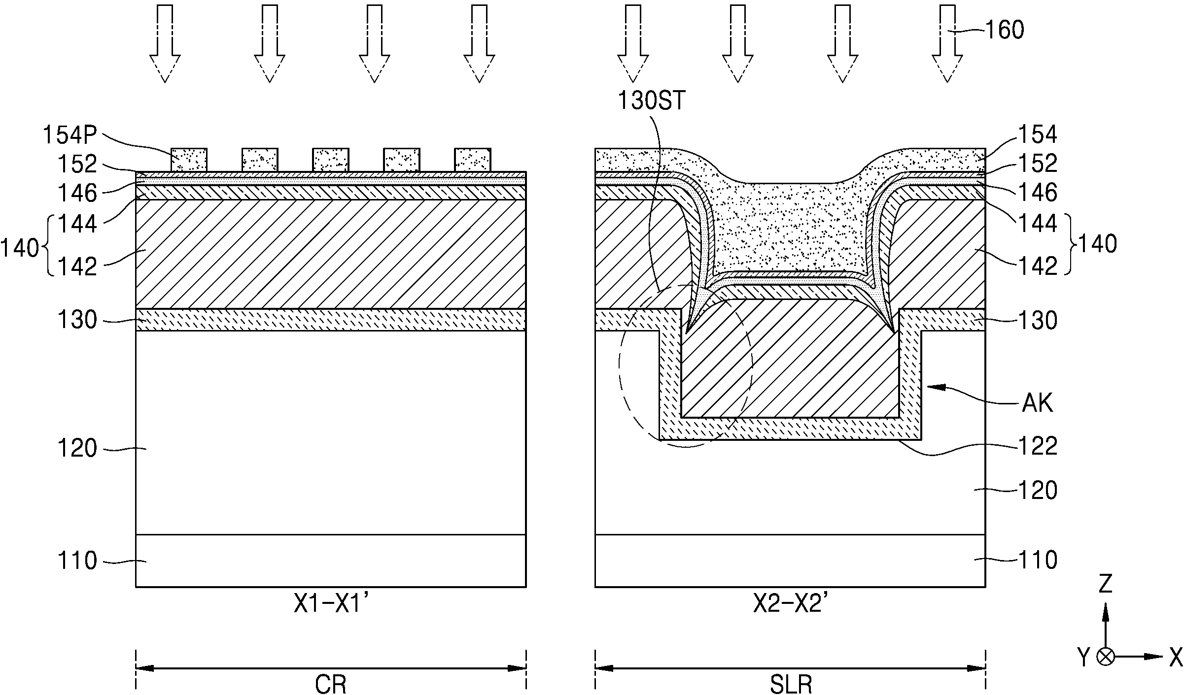
도 3a 내지 도 3h는 본 발명의 기술적 사상에 의한 실시예들에 따른 집적회로 소자의 제조 방법을 설명하기 위하여 공정 순서에 따라 도시한 단면도들이다. 도 3a 내지 도 3h를 참조하여, 도 2a 및 도 2b에 예시한 집적회로 소자(100)에 포함되는 복수의 아일랜드 패턴(PA) 및 얼라인먼트 키(AK)의 형성 방법을 설명한다. 도 3a 내지 도 3h에는 각각 도 2a의 (b)의 X1 - X1' 선 단면과 도 2b의 X2 - X2' 선 단면에 대응하는 영역의 공정 순서에 따른 단면 구성이 예시되어 있다. FIGS. 3A to 3H are cross-sectional views illustrating a method of manufacturing an integrated circuit device according to embodiments of the technical idea of the present invention in accordance with the process sequence. Referring to FIGS. 3A to 3H, a method of forming a plurality of island patterns (PAs) and alignment keys (AKs) included in the integrated circuit device (100) illustrated in FIGS. 2A and 2B will be described. FIGS. 3A to 3H illustrate cross-sectional configurations according to the process sequence of regions corresponding to the X1 - X1' line cross-section of FIG. 2A (b) and the X2 - X2' line cross-section of FIG. 2B, respectively.
도 3a를 참조하면, 기판(110) 상에 하부 구조물(120)을 형성하고, 하부 구조물(120) 위에 피쳐층(feature layer)(130)을 형성한다. Referring to FIG. 3a, a substructure (120) is formed on a substrate (110), and a feature layer (130) is formed on the substructure (120).
칩 영역(CR)에서 피쳐층(130)의 상면은 평탄하게 연장될 수 있다. The upper surface of the feature layer (130) in the chip region (CR) can be extended flatly.
스크라이브 레인 영역(SLR)에서 하부 구조물(120)의 상면에는 복수의 얼라인먼트 키(AK)(도 2b 참조)를 형성하는 데 필요한 트렌치(122)가 형성될 수 있다. 스크라이브 레인 영역(SLR)에서 피쳐층(130)은 하부 구조물(120)의 상면 및 트렌치(122)의 내벽을 컨포멀하게 덮도록 형성될 수 있다. 이에 따라, 스크라이브 레인 영역(SLR)에서 피쳐층(130)에는 도 3a에서 점선 영역으로 표시한 바와 같이 트렌치(122)의 주변에 비교적 큰 높이(SH)의 단차부(130ST)가 존재할 수 있다. 하부 구조물(120)의 트렌치(122)와, 그 위에 형성된 피쳐층(130)의 단차부(130ST)는 얼라인먼트 키(AK)를 구성할 수 있다. 피쳐층(130)은 복수의 아일랜드 패턴(PA)(도 2a 참조)의 구성 물질과 동일한 물질로 이루어질 수 있다.In the scribe lane region (SLR), a trench (122) necessary for forming a plurality of alignment keys (AK) (see FIG. 2b) may be formed on the upper surface of the lower structure (120). In the scribe lane region (SLR), the feature layer (130) may be formed to conformally cover the upper surface of the lower structure (120) and the inner wall of the trench (122). Accordingly, in the scribe lane region (SLR), a step portion (130ST) having a relatively large height (SH) may exist around the trench (122) in the feature layer (130), as indicated by the dotted line area in FIG. 3a. The trench (122) of the lower structure (120) and the step portion (130ST) of the feature layer (130) formed thereon may form an alignment key (AK). The feature layer (130) may be made of the same material as the constituent material of the plurality of island patterns (PA) (see FIG. 2a).
도 3b를 참조하면, 칩 영역(CR) 및 스크라이브 레인 영역(SLR)에서 피쳐층(130) 상에 제1 하드마스크층(142)을 형성한다. Referring to FIG. 3b, a first hard mask layer (142) is formed on the feature layer (130) in the chip region (CR) and the scribe lane region (SLR).
예시적인 실시예들에서, 제1 하드마스크층(142)은 ACL(amorphous carbon layer)로 이루어질 수 있다. 제1 하드마스크층(142)을 형성하기 위하여 CVD(chemical vapor deposition) 공정을 이용할 수 있다. 제1 하드마스크층(142)은 약 1000 Å 내지 약 2000 Å의 두께를 가질 수 있다. In exemplary embodiments, the first hard mask layer (142) may be formed of an amorphous carbon layer (ACL). A chemical vapor deposition (CVD) process may be used to form the first hard mask layer (142). The first hard mask layer (142) may have a thickness of about 1000 Å to about 2000 Å.
칩 영역(CR)에서, 제1 하드마스크층(142)은 위치에 따른 두께 편차가 거의 없이 실질적으로 일정한 두께를 가질 수 있다. 스크라이브 레인 영역(SLR)에서, 제1 하드마스크층(142)의 두께는 일정하지 않을 수 있다. 특히, 피쳐층(130)의 단차부(130ST) 및 그 주변 위에서는 제1 하드마스크층(142)의 스텝 커버리지(step coverage)가 열화되어, 단차부(130ST) 및 그 주변 위에서 제1 하드마스크층(142)의 일부가 다른 부분에 비해 현저히 작은 두께를 가질 수 있다. In the chip region (CR), the first hard mask layer (142) may have a substantially constant thickness with little thickness deviation depending on the location. In the scribe lane region (SLR), the thickness of the first hard mask layer (142) may not be constant. In particular, the step coverage of the first hard mask layer (142) may be degraded over the step portion (130ST) of the feature layer (130) and its surroundings, so that a part of the first hard mask layer (142) over the step portion (130ST) and its surroundings may have a significantly smaller thickness than other parts.
도 3c를 참조하면, 칩 영역(CR) 및 스크라이브 레인 영역(SLR)에서 제1 하드마스크층(142) 상에 제2 하드마스크층(144)을 형성한다. Referring to FIG. 3c, a second hard mask layer (144) is formed on the first hard mask layer (142) in the chip region (CR) and the scribe lane region (SLR).
예시적인 실시예들에서, 제2 하드마스크층(144)은 비정질 실리콘층으로 이루어질 수 있다. 제2 하드마스크층(144)을 형성하기 위하여 CVD 공정을 이용할 수 있다. 제2 하드마스크층(144)은 약 100 Å 내지 약 800 Å의 두께를 가질 수 있다. 제1 하드마스크층(142) 및 제2 하드마스크층(144)은 하드마스크 구조물(140)을 구성할 수 있다. In exemplary embodiments, the second hardmask layer (144) may be formed of an amorphous silicon layer. A CVD process may be used to form the second hardmask layer (144). The second hardmask layer (144) may have a thickness of about 100 Å to about 800 Å. The first hardmask layer (142) and the second hardmask layer (144) may form a hardmask structure (140).
칩 영역(CR)에서, 제2 하드마스크층(144)은 위치에 따른 두께 편차가 거의 없이 실질적으로 일정한 두께를 가질 수 있다. 스크라이브 레인 영역(SLR)에서, 제2 하드마스크층(144)의 두께는 일정하지 않을 수 있다. 특히, 피쳐층(130)의 단차부(130ST) 및 그 주변 위에서 제1 하드마스크층(142)을 덮는 제2 하드마스크층(144)의 일부는 스텝 커버리지가 열화되어, 단차부(130ST) 및 그 주변 위에서 제1 하드마스크층(142)을 덮는 제2 하드마스크층(144)의 일부가 다른 부분에 비해 현저히 작은 두께를 가질 수 있다. In the chip region (CR), the second hardmask layer (144) may have a substantially constant thickness with little thickness deviation depending on the location. In the scribe lane region (SLR), the thickness of the second hardmask layer (144) may not be constant. In particular, a part of the second hardmask layer (144) covering the first hardmask layer (142) over the step portion (130ST) of the feature layer (130) and its surroundings may have deteriorated step coverage, such that the part of the second hardmask layer (144) covering the first hardmask layer (142) over the step portion (130ST) and its surroundings may have a significantly smaller thickness than other parts.
도 3d를 참조하면, 칩 영역(CR) 및 스크라이브 레인 영역(SLR)에서 하드마스크 구조물(140) 상에 보호막(146)을 형성한다. Referring to FIG. 3d, a protective film (146) is formed on the hard mask structure (140) in the chip region (CR) and the scribe lane region (SLR).
보호막(146)은 칩 영역(CR) 및 스크라이브 레인 영역(SLR)에서 각각 실질적으로 균일한 두께를 가질 수 있다. 보호막(146) 중 피쳐층(130)의 단차부(130ST) 및 그 주변 위에서 제2 하드마스크층(144)을 덮는 부분은 보호막(146)의 다른 부분들보다 더 작은 두께를 가지지 않는다. 보호막(146)은 칩 영역(CR) 및 스크라이브 레인 영역(SLR)에서 하드마스크 구조물(140)이 외부로 노출되지 않도록 하드마스크 구조물(140)을 덮으며, 칩 영역(CR) 및 스크라이브 레인 영역(SLR)에서 하드마스크 구조물(140)의 보호에 필요한 최소한의 두께를 유지할 수 있다. The protective film (146) may have a substantially uniform thickness in each of the chip region (CR) and the scribe lane region (SLR). A portion of the protective film (146) that covers the second hard mask layer (144) over the step portion (130ST) of the feature layer (130) and its surroundings does not have a smaller thickness than other portions of the protective film (146). The protective film (146) covers the hard mask structure (140) so that the hard mask structure (140) is not exposed to the outside in the chip region (CR) and the scribe lane region (SLR), and may maintain a minimum thickness necessary for protecting the hard mask structure (140) in the chip region (CR) and the scribe lane region (SLR).
보호막(146)은 피쳐층(130) 및 하드마스크 구조물(140)을 주변 분위기로부터 보호하는 역할을 할 수 있다. 예시적인 실시예들에서, 보호막(146)은 제2 하드마스크층(144)의 상면에 접하도록 형성되고 제2 하드마스크층(144)의 산화를 방지하는 역할을 할 수 있다. 보호막(146)은 제2 하드마스크층(144)의 구성 물질과 다른 구성 물질로 이루어질 수 있다. 예시적인 실시예들에서, 보호막(146)은 산소 원자, 질소 원자, 또는 이들이 조합을 포함하는 실리콘 함유막으로 이루어질 수 있다. 예를 들면, 보호막(146)은 실리콘 산화막, 실리콘 질화막, 실리콘 산질화막, 또는 이들의 조합으로 이루어질 수 있다. The protective film (146) may serve to protect the feature layer (130) and the hard mask structure (140) from the surrounding atmosphere. In exemplary embodiments, the protective film (146) is formed to contact the upper surface of the second hard mask layer (144) and may serve to prevent oxidation of the second hard mask layer (144). The protective film (146) may be made of a different material from the material of the second hard mask layer (144). In exemplary embodiments, the protective film (146) may be made of a silicon-containing film including oxygen atoms, nitrogen atoms, or a combination thereof. For example, the protective film (146) may be made of a silicon oxide film, a silicon nitride film, a silicon oxynitride film, or a combination thereof.
보호막(146)을 형성하기 위하여 ALD(atomic layer deposition) 공정을 이용할 수 있다. 보호막(146)은 약 10 Å 내지 약 500 Å의 두께를 가질 수 있다. 예시적인 실시예들에서, 보호막(146)은 제2 하드마스크층(144)의 두께보다 더 작은 두께를 가질 수 있다. 예를 들면, 제2 하드마스크층(144)은 약 150 Å 내지 약 250 Å의 두께를 가지고, 보호막(146)은 약 20 Å 내지 약 80 Å의 두께를 가질 수 있으나, 제2 하드마스크층(144) 및 보호막(146) 각각의 두께가 상기 예시한 바에 한정되는 것은 아니다. An ALD (atomic layer deposition) process may be used to form the protective film (146). The protective film (146) may have a thickness of about 10 Å to about 500 Å. In exemplary embodiments, the protective film (146) may have a thickness smaller than the thickness of the second hard mask layer (144). For example, the second hard mask layer (144) may have a thickness of about 150 Å to about 250 Å, and the protective film (146) may have a thickness of about 20 Å to about 80 Å, but the thicknesses of each of the second hard mask layer (144) and the protective film (146) are not limited to those exemplified above.
도 3e를 참조하면, 보호막(146) 상에 레지스트 하부막(underlayer)(152) 및 포토레지스트막(154)을 차례로 형성한다. Referring to FIG. 3e, a resist underlayer (152) and a photoresist film (154) are sequentially formed on a protective film (146).
예시적인 실시예들에서, 레지스트 하부막(152)은 폴리머로 이루어질 수 있다. 예를 들면, 레지스트 하부막(152)은 폴리실록산으로 이루어질 수 있다. 상기 폴리실록산은 실록산 결합을 갖는 중합체로서, 모노실록산(monosiloxane), 디실록산(disiloxane), 트리실록산(trisiloxane), 및/또는 시클로테트라실록산(cyclotetrasiloxane)으로 이루어지는 반복 단위를 포함할 수 있다. In exemplary embodiments, the resist sublayer (152) may be formed of a polymer. For example, the resist sublayer (152) may be formed of a polysiloxane. The polysiloxane is a polymer having a siloxane bond and may include repeating units formed of monosiloxane, disiloxane, trisiloxane, and/or cyclotetrasiloxane.
레지스트 하부막(152)은 광산발생제(photoacid generator), 가교제, 및 계면 접착 강화제 중 적어도 하나를 포함할 수 있다. 상기 광산발생제는 빛에 의하여 산을 발생시킬 수 있는 화합물로서, 예를 들면 트리페닐설포늄 트리플루오르메탄술포네이트(triphenylsulfonium trifluoromethanesulfonate)를 포함하는 오늄염(onium salt), 방향족 디아조늄염(aromatic diazonium salt), 술포늄염(sulfonium slat), 트리아릴술포늄염(triarylsulfonium salt), 디아릴술포늄염(diarylsulfonium salt), 모노아릴술포늄염(monoarylsulfonium salt), 요오드염(iodonium salt), 디아릴요오드염(diaryliodonium salt), 니트로벤질 에스테르(nitrobenzyl ester), 디술폰(disulfone), 디아조-디술폰(diazo-disulfone), 술포네이트(sulfonate), 트리클로로메틸 트리아진(trichloromethyl triazine) 및 N-히드록시숙신이미드 트리플레이트(N-hydroxysuccinimide triflate) 등을 포함할 수 있다. 상기 가교제는 상기 폴리실록산의 반복 단위를 가교하기 위한 것으로서 예를 들어, 멜라민, 우레아, 다가 알콜(polyhydric alcohol) 등을 포함할 수 있다. 상기 계면 접착 강화제는 후속의 포토레지스트막(154) 현상 공정에서 발생할 수 있는 패턴의 무너짐 또는 박리를 방지하기 위하여 레지스트 하부막(152)과 포토레지스트막(154)과의 사이의 밀착성을 향상시키기 위한 것으로서 히드록실기를 포함하는 모노머 유니트를 가지는 폴리머로 이루어질 수 있다. The resist sublayer (152) may include at least one of a photoacid generator, a crosslinking agent, and an interfacial adhesion enhancer. The photoacid generator is a compound capable of generating an acid by light, and examples thereof include an onium salt including triphenylsulfonium trifluoromethanesulfonate, an aromatic diazonium salt, a sulfonium salt, a triarylsulfonium salt, a diarylsulfonium salt, a monoarylsulfonium salt, an iodonium salt, a diaryliodonium salt, a nitrobenzyl ester, a disulfone, a diazo-disulfone, a sulfonate, trichloromethyl triazine, and N-hydroxysuccinimide triflate. may include, for example, melamine, urea, polyhydric alcohol, etc. The crosslinking agent is for crosslinking the repeating unit of the polysiloxane, and may include, for example, melamine, urea, polyhydric alcohol, etc. The interfacial adhesion reinforcing agent is for improving the adhesion between the resist lower layer (152) and the photoresist film (154) in order to prevent collapse or peeling of the pattern that may occur in the subsequent photoresist film (154) developing process, and may be made of a polymer having a monomer unit containing a hydroxyl group.
다른 예시적인 실시예들에서, 레지스트 하부막(152)은 반사방지막(Bottom Anti-Reflective Coating: BARC)으로 이루어질 수 있다. 상기 반사방지막은 유기 화합물, 무기 화합물, 또는 이들의 조합으로 이루어질 수 있다. 예를 들면, 상기 반사방지막은 실리콘 질화물, 실리콘 산질화물, 비정질 실리콘, 티탄, 이산화티탄, 질화티탄, 산화크롬, 카본, 유기 ARC(anti-reflective coating) 재료, 또는 이들의 조합으로 이루어질 수 있다. 상기 유기 ARC(anti-reflective coating) 재료는 가교 반응기인 히드록실기와 흡광기를 동일 분자내에 갖는 아크릴 수지, 또는 가교 반응기인 히드록실기와 흡광기를 동일 분자내에 갖는 노볼락 수지로 이루어질 수 있으나, 이들에 한정되는 것은 아니다. In other exemplary embodiments, the resist lower layer (152) may be formed of an anti-reflective coating (Bottom Anti-Reflective Coating: BARC). The anti-reflective coating may be formed of an organic compound, an inorganic compound, or a combination thereof. For example, the anti-reflective coating may be formed of silicon nitride, silicon oxynitride, amorphous silicon, titanium, titanium dioxide, titanium nitride, chromium oxide, carbon, an organic ARC (anti-reflective coating) material, or a combination thereof. The organic ARC (anti-reflective coating) material may be formed of an acrylic resin having a crosslinking reactive group, a hydroxyl group, and a light absorbing group in the same molecule, or a novolac resin having a crosslinking reactive group, a hydroxyl group, and a light absorbing group in the same molecule, but is not limited thereto.
레지스트 하부막(152)을 형성하기 위하여, 스핀 코팅, CVD, 또는 ALD 공정을 이용할 수 있다. 레지스트 하부막(152)은 약 10 Å 내지 약 400 Å의 두께를 가질 수 있다. To form the resist lower film (152), spin coating, CVD, or ALD process can be used. The resist lower film (152) can have a thickness of about 10 Å to about 400 Å.
포토레지스트막(154)은 EUV(extreme ultraviolet)(13.5 nm)용 레지스트, KrF 엑시머 레이저(248 nm)용 레지스트, ArF 엑시머 레이저(193 nm)용 레지스트, 또는 F2 엑시머 레이저(157 nm)용 레지스트로 이루어질 수 있다. 포토레지스트막(154)은 약 100 Å 내지 약 800 Å의 두께를 가질 수 있다. The photoresist film (154) may be formed of a resist for an extreme ultraviolet (EUV) (13.5 nm), a resist for a KrF excimer laser (248 nm), a resist for an ArF excimer laser (193 nm), or a resist for an F 2 excimer laser (157 nm). The photoresist film (154) may have a thickness of about 100 Å to about 800 Å.
도 3f를 참조하면, 칩 영역(CR)에서 포토레지스트막(154)을 노광 및 현상하여, 포토레지스트막(154)으로부터 포토레지스트 패턴(154P)을 형성한다. 스크라이브 레인 영역(SLR)에서는 포토레지스트막(154)의 노광 및 현상 공정이 이루어지지 않을 수 있다. 포토레지스트막(154)을 노광하는 데 있어서, 광원으로서 EUV(13.5 nm), KrF 엑시머 레이저(248 nm), ArF 엑시머 레이저, 또는 F2 엑시머 레이저(157 nm)를 이용할 수 있다. 칩 영역(CR)에서, 포토레지스트 패턴(150P)은 칩 영역(CR)에 형성될 복수의 아일랜드 패턴(PA)(도 2a 참조)의 평면 형상과 동일한 평면 형상을 가질 수 있다. 포토레지스트 패턴(150P)은 서로 이격되고 규칙적인 배열을 이루는 복수의 아일랜드 패턴으로 이루어질 수 있다. Referring to FIG. 3F, a photoresist film (154) is exposed and developed in the chip region (CR) to form a photoresist pattern (154P) from the photoresist film (154). The exposure and development process of the photoresist film (154) may not be performed in the scribe lane region (SLR). In exposing the photoresist film (154), an EUV (13.5 nm), a KrF excimer laser (248 nm), an ArF excimer laser, or an F 2 excimer laser (157 nm) may be used as a light source. In the chip region (CR), the photoresist pattern (150P) may have the same planar shape as the planar shape of a plurality of island patterns (PA) (see FIG. 2A) to be formed in the chip region (CR). The photoresist pattern (150P) may be formed of a plurality of island patterns that are spaced apart from each other and have a regular arrangement.
도 3g를 참조하면, 도 3f의 결과물에서 포토레지스트 패턴(154P)의 형상을 피쳐층(130)에 전사하여 피쳐 패턴(130P)을 형성한다. Referring to FIG. 3g, the shape of the photoresist pattern (154P) in the result of FIG. 3f is transferred to the feature layer (130) to form a feature pattern (130P).
보다 상세히 설명하면, 도 3f의 결과물에서 포토레지스트 패턴(154P)을 식각 마스크로 이용하여, 칩 영역(CR)에서 레지스트 하부막(152), 보호막(146), 및 하드마스크 구조물(140)을 차례로 이방성 식각할 수 있다. 그 결과, 하드마스크 구조물(140)의 식각에 의해 칩 영역(CR)에 하드마스크 구조물 패턴(140P)이 얻어질 수 있다. 칩 영역(CR)에 있는 하드마스크 구조물 패턴(140P)과 스크라이브 레인 영역(SLR)에 있는 하드마스크 구조물(140)을 식각 마스크로 이용하여 피쳐층(130)을 이방성 식각하여 칩 영역(CR)에 피쳐 패턴(130P)을 형성할 수 있다. 피쳐 패턴(130P)은 도 2a에 예시한 복수의 아일랜드 패턴(PA)을 구성할 수 있다. In more detail, in the result of FIG. 3f, the photoresist pattern (154P) can be used as an etching mask to sequentially anisotropically etch the resist lower layer (152), the protective layer (146), and the hardmask structure (140) in the chip area (CR). As a result, a hardmask structure pattern (140P) can be obtained in the chip area (CR) by etching the hardmask structure (140). The feature layer (130) can be anisotropically etched using the hardmask structure pattern (140P) in the chip area (CR) and the hardmask structure (140) in the scribe lane area (SLR) as etching masks to form a feature pattern (130P) in the chip area (CR). The feature pattern (130P) can configure a plurality of island patterns (PA) as exemplified in FIG. 2a.
피쳐 패턴(130P)을 형성하기 위한 식각 공정 중에 하드마스크 구조물(140) 위에 있던 포토레지스트 패턴(154P), 하부막(152), 및 보호막(146) 중 적어도 일부가 식각 분위기에 의해 소모될 수 있다. 도 3g에는 칩 영역(CR)에서 피쳐 패턴(130P) 상에 하드마스크 구조물 패턴(140P)을 구성하는 제1 하드마스크층(142) 및 제2 하드마스크층(144)이 남아 있는 경우를 예시하였으나, 상기 식각 분위기에 의해 제2 하드마스크층(144)도 소모될 수 있으며, 피쳐 패턴(130P) 상에는 제1 하드마스크층(142)의 일부만 남게 될 수도 있다. During the etching process for forming the feature pattern (130P), at least a portion of the photoresist pattern (154P), the lower film (152), and the protective film (146) that were on the hard mask structure (140) may be consumed by the etching atmosphere. FIG. 3g illustrates an example in which the first hard mask layer (142) and the second hard mask layer (144) constituting the hard mask structure pattern (140P) remain on the feature pattern (130P) in the chip region (CR), but the second hard mask layer (144) may also be consumed by the etching atmosphere, and only a portion of the first hard mask layer (142) may remain on the feature pattern (130P).
예시적인 실시예들에서, 피쳐 패턴(130P)이 형성된 후 과도 식각에 의해 하부 구조물(120)의 일부가 식각되어 칩 영역(CR)에서 하부 구조물(120)의 상면 중 피쳐 패턴(130P)을 통해 노출되는 일부 영역에 리세스 영역(도시 생략)이 형성될 수 있다. 다른 예시적인 실시예들에서, 칩 영역(CR)에서 하부 구조물(120)의 상면에는 위에서 설명한 바와 같은 리세스 영역이 형성되지 않을 수도 있다. In exemplary embodiments, after the feature pattern (130P) is formed, a portion of the lower structure (120) may be etched by over-etching to form a recess region (not shown) in a portion of the upper surface of the lower structure (120) in the chip region (CR) that is exposed through the feature pattern (130P). In other exemplary embodiments, the recess region as described above may not be formed on the upper surface of the lower structure (120) in the chip region (CR).
도 3h를 참조하면, 피쳐 패턴(130P) 상에 남아 있는 불필요한 물질들을 제거하여 피쳐 패턴(130P)의 상면을 노출시킨다. 이를 위하여, 애싱 및 스트립 공정을 이용할 수 있다. 스크라이브 레인 영역(SLR)에서는 얼라인먼트 키(AK)를 구성하는 피쳐층(130)의 상면이 다시 노출될 수 있다. Referring to FIG. 3h, unnecessary materials remaining on the feature pattern (130P) are removed to expose the upper surface of the feature pattern (130P). For this purpose, an ashing and stripping process can be used. In the scribe lane area (SLR), the upper surface of the feature layer (130) constituting the alignment key (AK) can be exposed again.
도 4a 내지 도 4c는 본 발명의 기술적 사상에 의한 다른 실시예들에 따른 집적회로 소자의 제조 방법을 설명하기 위하여 공정 순서에 따라 도시한 단면도들이다. 도 4a 내지 도 4c를 참조하여, 도 2a 및 도 2b에 예시한 집적회로 소자(100)에 포함되는 복수의 아일랜드 패턴(PA) 및 얼라인먼트 키(AK)의 다른 형성 방법을 설명한다. 도 4a 및 도 4b에는 각각 도 2a의 (b)의 X1 - X1' 선 단면과 도 2b의 X2 - X2' 선 단면에 대응하는 영역의 공정 순서에 따른 단면 구성이 예시되어 있다. FIGS. 4A to 4C are cross-sectional views illustrating a manufacturing method of an integrated circuit device according to other embodiments of the technical idea of the present invention in accordance with the process sequence. Referring to FIGS. 4A to 4C, another method of forming a plurality of island patterns (PAs) and alignment keys (AKs) included in the integrated circuit device (100) illustrated in FIGS. 2A and 2B will be described. FIGS. 4A and 4B illustrate cross-sectional configurations according to the process sequence of regions corresponding to the X1 - X1' line cross-section of FIG. 2A (b) and the X2 - X2' line cross-section of FIG. 2B, respectively.
도 4a를 참조하면, 도 3a 및 도 3f를 참조하여 설명한 바와 같은 방법으로 기판(110) 상에 포토레지스트 패턴(154P)을 형성하는 공정까지 수행한다. 그 후, 포토레지스트 패턴(154P)을 검사하여 포토레지스트 패턴(154P)의 정렬 상태 및 불량 여부를 확인한다. 포토레지스트 패턴(154P)의 검사 결과 포토레지스트 패턴(154P)이 불량으로 판단되면, 후속의 식각 공정에서 포토레지스트 패턴(154P)을 식각 마스크로 사용하기 어려우며, 포토레지스트 패턴(154P)을 제거하고 새로운 포토레지스트 패턴을 형성하기 위한 재작업(rework) 공정을 수행할 필요가 있다. 예를 들면, 포토레지스트 패턴(154P)의 검사 결과, 포토레지스트 패턴(154P)이 구불구불하게 휘어진 형상을 가지는 위글링(wiggling) 현상, 포토레지스트 패턴(154P)의 표면이 거칠게 되는 스트리에이션(striation) 현상, 포토레지스트 패턴(154P)의 쓰러짐 현상, 또는 포토레지스트 패턴(154P)의 정렬 상태가 허용 오차 한계를 벗어나는 현상이 발생된 경우 포토레지스트 패턴(154P)이 불량이라고 판단할 수 있다. Referring to FIG. 4A, a process of forming a photoresist pattern (154P) on a substrate (110) is performed in the same manner as described with reference to FIGS. 3A and 3F. Thereafter, the photoresist pattern (154P) is inspected to determine the alignment state and defects of the photoresist pattern (154P). If the photoresist pattern (154P) is determined to be defective as a result of the inspection of the photoresist pattern (154P), it is difficult to use the photoresist pattern (154P) as an etching mask in a subsequent etching process, and it is necessary to perform a rework process to remove the photoresist pattern (154P) and form a new photoresist pattern. For example, if, as a result of the inspection of the photoresist pattern (154P), a wiggling phenomenon in which the photoresist pattern (154P) has a crooked shape, a striation phenomenon in which the surface of the photoresist pattern (154P) becomes rough, a collapse phenomenon in the photoresist pattern (154P), or a phenomenon in which the alignment of the photoresist pattern (154P) exceeds the allowable error limit occurs, the photoresist pattern (154P) can be determined to be defective.
상기 재작업을 위하여, 칩 영역(CR)에 있는 포토레지스트 패턴(154P)과 스크라이브 레인 영역(SLR)에 있는 포토레지스트막(154)을 재작업 분위기(160)에 노출시킬 수 있다. For the above rework, the photoresist pattern (154P) in the chip area (CR) and the photoresist film (154) in the scribe lane area (SLR) can be exposed to a rework atmosphere (160).
예시적인 실시예들에서, 재작업 분위기(160)는 산소 함유 분위기를 포함할 수 있다. 예를 들면, 칩 영역(CR)에 있는 포토레지스트 패턴(154P)과 스크라이브 레인 영역(SLR)에 있는 포토레지스트막(154)을 산소 함유 분위기 하에서 플라즈마 애싱(ashing) 공정으로 제거할 수 있다. 다른 예에서 포토레지스트 패턴(154P) 및 포토레지스트막(154)을 제거하기 위하여 산소 함유 분위기 하에서 자외선을 조사하여 오존(O3) 및/또는 산소 라디칼(oxygen radical)을 발생시키고 이들을 이용하여 포토레지스트 패턴(154P) 및 포토레지스트막(154)을 CO2와 H2O로 분해시킬 수 있다. 레지스트 하부막(152)이 폴리머 또는 유기 화합물로 이루어진 경우, 칩 영역(CR)에 있는 포토레지스트 패턴(154P) 및 스크라이브 레인 영역(SLR)에 있는 포토레지스트막(154)의 제거시 레지스트 하부막(152)도 함께 제거될 수 있다. In exemplary embodiments, the rework atmosphere (160) may include an oxygen-containing atmosphere. For example, the photoresist pattern (154P) in the chip region (CR) and the photoresist film (154) in the scribe lane region (SLR) may be removed by a plasma ashing process under an oxygen-containing atmosphere. In another example, in order to remove the photoresist pattern (154P) and the photoresist film (154), ultraviolet rays may be irradiated under an oxygen-containing atmosphere to generate ozone (O 3 ) and/or oxygen radicals, which may be used to decompose the photoresist pattern (154P) and the photoresist film (154) into CO 2 and H 2 O. When the resist lower film (152) is made of a polymer or an organic compound, the resist lower film (152) may also be removed when the photoresist pattern (154P) in the chip area (CR) and the photoresist film (154) in the scribe lane area (SLR) are removed.
다른 예시적인 실시예들에서, 재작업 분위기(160)는 씨너(thinner) 조성물을 포함하는 습식 분위기일 수 있다. 상기 씨너 조성물은 에틸 락테이트(ethyl lactate), 에틸-3-에톡시 프로피오네이트(ethyl-3-ethoxy propionate), 감마부티로 락톤(gamma-butyro lactone), 아세톤, 에스테르 화합물, 프로필렌글리콜 알킬 에테르 아세테이트, 시클로케톤, 및 메틸 2-히드록시 이소부티레이트 중에서 선택되는 적어도 하나의 화합물을 포함할 수 있으나, 상기 씨너 조성물에 포함될 수 있는 화합물의 종류가 상기 예시한 바에 한정되는 것은 아니다. In other exemplary embodiments, the rework atmosphere (160) may be a wet atmosphere comprising a thinner composition. The thinner composition may comprise at least one compound selected from ethyl lactate, ethyl-3-ethoxy propionate, gamma-butyro lactone, acetone, an ester compound, a propylene glycol alkyl ether acetate, a cycloketone, and methyl 2-hydroxy isobutyrate, but the types of compounds that may be included in the thinner composition are not limited to those exemplified above.
도 4b를 참조하면, 도 4a를 참조하여 설명한 바와 같은 방법으로 칩 영역(CR)에 있는 포토레지스트 패턴(154P)과 스크라이브 레인 영역(SLR)에 있는 포토레지스트막(154)을 제거한 후, 칩 영역(CR) 및 스크라이브 레인 영역(SLR)에서 각각 보호막(146)이 노출될 수 있다. Referring to FIG. 4b, after the photoresist pattern (154P) in the chip area (CR) and the photoresist film (154) in the scribe lane area (SLR) are removed in the same manner as described with reference to FIG. 4a, the protective film (146) can be exposed in each of the chip area (CR) and the scribe lane area (SLR).
도 4a를 참조하여 설명한 재작업을 수행하는 동안 보호막(146)은 하부의 하드마스크 구조물(140)을 재작업 분위기(160)로부터 보호하는 역할을 할 수 있다. During the reworking described with reference to FIG. 4a, the protective film (146) may serve to protect the underlying hard mask structure (140) from the reworking atmosphere (160).
예를 들면, 보호막(146)이 생략된 경우, 도 4a를 참조하여 설명한 바와 같은 방법으로 포토레지스트 패턴(154P) 및 포토레지스트막(154)을 제거하는 동안 하드마스크 구조물(140)이 재작업 분위기(160)에 노출될 수 있다. 이 경우, 스크라이브 레인 영역(SLR)에서 제1 하드마스크층(142) 및 제2 하드마스크층(144)은 각각 피쳐층(130)의 단차부(130ST) 주변에서 열화된 스텝 커버리지로 인해 다른 부분보다 현저히 작은 두께를 가지는 취약 부분들을 포함하게 되고, 상기 취약 부분들을 통해 재작업 분위기(160)에 포함된 산소 원자 또는 씨너 조성물이 침투하여 단차부(130ST) 주변에서 피쳐층(130), 제1 하드마스크층(142), 및/또는 제2 하드마스크층(144)이 일부 제거되거나 손상될 수 있다. 이와 같은 결과가 발생하면, 스크라이브 레인 영역(SLR)에 있는 얼라인먼트 키(AK)가 정상적인 얼라인 키 역할을 수행할 수 없게 된다. For example, when the protective film (146) is omitted, the hardmask structure (140) may be exposed to the rework atmosphere (160) while the photoresist pattern (154P) and the photoresist film (154) are removed in the manner described with reference to FIG. 4A. In this case, in the scribe lane region (SLR), the first hardmask layer (142) and the second hardmask layer (144) each include weak portions having a significantly smaller thickness than other portions due to the degraded step coverage around the step portion (130ST) of the feature layer (130), and oxygen atoms or thinner compositions included in the rework atmosphere (160) may penetrate through the weak portions, causing the feature layer (130), the first hardmask layer (142), and/or the second hardmask layer (144) to be partially removed or damaged around the step portion (130ST). When this happens, the alignment key (AK) in the scribe lane area (SLR) cannot perform its normal alignment key function.
본 발명의 기술적 사상에 의하면, 하드마스크 구조물(140)의 최상층인 제2 하드마스크층(144)이 보호막(146)으로 덮여 있고, 특히 피쳐층(130)의 단차부(130ST)의 주변에서 제2 하드마스크층(144)이 노출되지 않도록 보호막(146)이 제2 하드마스크층(144)을 덮고 있으므로, 도 4a를 참조하여 설명한 바와 같은 방법으로 포토레지스트 패턴(154P) 및 포토레지스트막(154)을 제거하는 동안 스크라이브 레인 영역(SLR)에서 피쳐층(130) 및 하드마스크 구조물(140)이 손상되거나 변형될 염려가 없다. 따라서, 후속 공정에서 보호막(146) 위에 새로운 포토레지스트 패턴을 형성하기 위한 포토리소그래피 공정을 수행할 때 스크라이브 레인 영역(SLR)에 있는 얼라인먼트 키(AK)를 이용하여 정밀한 제어를 원활하게 수행할 수 있다. According to the technical idea of the present invention, since the second hardmask layer (144), which is the uppermost layer of the hardmask structure (140), is covered with a protective film (146), and especially, since the protective film (146) covers the second hardmask layer (144) so that the second hardmask layer (144) is not exposed around the step portion (130ST) of the feature layer (130), there is no concern that the feature layer (130) and the hardmask structure (140) will be damaged or deformed in the scribe lane area (SLR) while removing the photoresist pattern (154P) and the photoresist film (154) in the manner described with reference to FIG. 4A. Accordingly, when performing a photolithography process for forming a new photoresist pattern on the protective film (146) in a subsequent process, precise control can be smoothly performed using the alignment key (AK) in the scribe lane area (SLR).
도 4c를 참조하면, 도 4b의 결과물의 칩 영역(CR) 및 스크라이브 레인 영역(SLR)에서 도 3e를 참조하여 설명한 바와 유사한 방법으로 보호막(146)을 덮는 레지스트 하부막(172) 및 포토레지스트막(174)을 차례로 형성한 후, 도 3f를 참조하여 설명한 바와 유사한 방법으로 스크라이브 레인 영역(SLR)에 있는 얼라인먼트 키(AK)를 이용하여 칩 영역(CR)에서 포토레지스트막(174)을 노광 및 현상하여, 포토레지스트막(174)으로부터 포토레지스트 패턴(174P)을 형성한다. Referring to FIG. 4c, a resist lower film (172) and a photoresist film (174) covering a protective film (146) are sequentially formed in the chip area (CR) and the scribe lane area (SLR) of the resultant of FIG. 4b in a similar manner to that described with reference to FIG. 3e, and then, using an alignment key (AK) in the scribe lane area (SLR) in a similar manner to that described with reference to FIG. 3f, the photoresist film (174) is exposed and developed in the chip area (CR), thereby forming a photoresist pattern (174P) from the photoresist film (174).
예시적인 실시예들에서, 포토레지스트 패턴(174P)이 형성된 후, 도 4a 내지 도 4c를 참조하여 설명한 바와 유사한 방법으로 포토레지스트 패턴(174P)의 검사 공정, 재작업 공정, 및 새로운 포토레지스트 패턴 형성 공정을 적어도 1 회 더 수행할 수 있다. 그 후, 도 3g 및 도 3h를 참조하여 설명한 공정들을 수행하여, 칩 영역(CR)에는 하부 구조물(120) 상에 피쳐 패턴(130P)을 형성하고, 스크라이브 레인 영역(SLR)에서는 얼라인먼트 키(AK)를 구성하는 피쳐층(130)의 상면을 다시 노출시킬 수 있다. In exemplary embodiments, after the photoresist pattern (174P) is formed, the inspection process, the reworking process, and the new photoresist pattern forming process of the photoresist pattern (174P) may be performed at least once more in a manner similar to that described with reference to FIGS. 4A to 4C . Thereafter, by performing the processes described with reference to FIGS. 3G and 3H , the feature pattern (130P) may be formed on the lower structure (120) in the chip region (CR), and the upper surface of the feature layer (130) constituting the alignment key (AK) may be re-exposed in the scribe lane region (SLR).
도 4a 내지 도 4c를 참조하여 설명한 본 발명의 기술적 사상에 의한 실시예들에 따른 집적회로 소자의 제조 방법에 의하면, 칩 영역(CR)에서 피쳐층(130)을 패터닝하기 위하여 포토리소그래피 공정을 수행할 때 하드마스크 구조물(140) 상에 하드마스크 구조물(140)을 보호하기 위한 보호막(146)을 형성하고, 보호막(146) 위에 포토레지스트막(154)을 형성하기 위한 포토리소그래피 공정을 수행한다. 따라서, 포토레지스트막(154)을 형성한 후 이를 다시 제거하고 새로운 포토레지스트막(174)을 형성하기 위한 재작업을 수행할 때, 스크라이브 레인 영역(SLR)에 있는 피쳐층(130)의 단차부(130ST)의 주변에서 하드마스크 구조물(140)의 열화된 스텝 커버리지로 인해 하드마스크 구조물(140)의 일부 영역이 재작업 분위기(160)에 취약한 부분을 포함하는 경우에도, 하드마스크 구조물(140)이 보호막(146)으로 덮여 있으므로 재작업을 수행하는 동안 스크라이브 레인 영역(SLR)에서 피쳐층(130) 및/또는 하드마스크 구조물(140)이 손상되거나 변형될 염려가 없다. 따라서, 후속 공정에서 보호막(146) 위에 새로운 포토레지스트 패턴(174P)을 형성하기 위한 포토리소그래피 공정을 수행할 때 스크라이브 레인 영역(SLR)에 있는 얼라인먼트 키(AK)를 이용하는 정밀한 제어를 원활하게 수행할 수 있다. According to a method for manufacturing an integrated circuit device according to embodiments of the technical idea of the present invention described with reference to FIGS. 4A to 4C, when performing a photolithography process to pattern a feature layer (130) in a chip region (CR), a protective film (146) for protecting a hard mask structure (140) is formed on a hard mask structure (140), and a photolithography process is performed to form a photoresist film (154) on the protective film (146). Accordingly, when performing reworking to form a new photoresist film (174) after forming the photoresist film (154) and then removing it, even if some areas of the hardmask structure (140) include a portion vulnerable to the reworking atmosphere (160) due to the deteriorated step coverage of the hardmask structure (140) around the step portion (130ST) of the feature layer (130) in the scribe lane region (SLR), there is no concern that the feature layer (130) and/or the hardmask structure (140) in the scribe lane region (SLR) will be damaged or deformed during the reworking since the hardmask structure (140) is covered with the protective film (146). Accordingly, when performing a photolithography process to form a new photoresist pattern (174P) on a protective film (146) in a subsequent process, precise control using an alignment key (AK) in a scribe lane area (SLR) can be smoothly performed.
도 5는 본 발명의 기술적 사상에 의한 다른 실시예들에 따른 집적회로 소자(200)의 예시적인 구성을 설명하기 위한 블록도이다. FIG. 5 is a block diagram for explaining an exemplary configuration of an integrated circuit device (200) according to other embodiments according to the technical idea of the present invention.
도 5를 참조하면, 집적회로 소자(200)는 도 1에 예시한 집적회로 소자(100)의 복수의 칩 영역(CR) 중 일부를 구성할 수 있다. 집적회로 소자(200)의 칩 영역(CR)은 제1 영역(22) 및 제2 영역(24)을 포함할 수 있다. 제1 영역(22)은 DRAM 소자의 메모리 셀 영역이고, 제2 영역(24)은 DRAM 소자의 주변 회로 영역일 수 있다. 제1 영역(22)은 메모리 셀 어레이(22A)를 포함할 수 있다. 제2 영역(24)은 로우 디코더(52), 센스 앰프(54), 칼럼 디코더(56), 셀프 리프레쉬 제어 회로(58), 커맨드 디코더(60), MRS/EMRS(Mode Register Set/Extended Mode Register Set) 회로(62), 어드레스 버퍼(64), 및 데이터 입출력 회로(66)를 구비할 수 있다. Referring to FIG. 5, the integrated circuit device (200) may constitute a part of a plurality of chip regions (CR) of the integrated circuit device (100) illustrated in FIG. 1. The chip region (CR) of the integrated circuit device (200) may include a first region (22) and a second region (24). The first region (22) may be a memory cell region of a DRAM device, and the second region (24) may be a peripheral circuit region of the DRAM device. The first region (22) may include a memory cell array (22A). The second region (24) may include a row decoder (52), a sense amplifier (54), a column decoder (56), a self-refresh control circuit (58), a command decoder (60), an MRS/EMRS (Mode Register Set/Extended Mode Register Set) circuit (62), an address buffer (64), and a data input/output circuit (66).
도 6은 도 5에 예시한 집적회로 소자(200)의 예시적인 배치 구성을 설명하기 위한 평면도이다. FIG. 6 is a plan view for explaining an exemplary arrangement configuration of the integrated circuit element (200) illustrated in FIG. 5.
도 6을 참조하면, 집적회로 소자(200)의 칩 영역(CR)은 스크라이브 레인 영역(SLR)으로 포위될 수 있다. 집적회로 소자(200)의 칩 영역(CR)은 복수의 제1 영역(22)을 포함하고, 복수의 제1 영역(22)은 각각 제2 영역(24)으로 포위될 수 있다. 제1 영역(22)은 각각 DRAM 소자의 셀 어레이 영역(MCA)이고, 제2 영역(24)은 DRAM 소자의 주변 회로들이 형성되는 주변회로 영역 및 코어 영역일 수 있다. Referring to FIG. 6, the chip region (CR) of the integrated circuit device (200) may be surrounded by a scribe lane region (SLR). The chip region (CR) of the integrated circuit device (200) includes a plurality of first regions (22), and each of the plurality of first regions (22) may be surrounded by a second region (24). Each of the first regions (22) may be a cell array region (MCA) of the DRAM device, and the second region (24) may be a peripheral circuit region and a core region where peripheral circuits of the DRAM device are formed.
제1 영역(22)에서 셀 어레이 영역(MCA)은 도 5를 참조하여 설명한 메모리 셀 어레이(22A)를 포함할 수 있다. 제2 영역(24)은 서브 워드 라인 드라이버(sub-word line driver) 블록(SWD), 센스앰프 블록(S/A), 및 컨정션 블록(CJT)을 포함할 수 있다. 센스앰프 블록(S/A)에는 복수의 비트 라인 센스 앰프가 배치될 수 있다. 컨정션 블록(CJT)은 서브 워드 라인 드라이버 블록(SWD)과 센스앰프 블록(S/A)이 교차하는 지점에 배치될 수 있다. 컨정션 블록(CJT)에는 비트 라인 센스앰프를 구동하기 위한 전원 드라이버들 및 접지 드라이버들이 교대로 배치될 수 있다. 제2 영역(24)에는 인버터 체인(inverter chain), 입출력 회로 등과 같은 주변 회로가 더 형성될 수 있다. In the first region (22), the cell array region (MCA) may include a memory cell array (22A) described with reference to FIG. 5. The second region (24) may include a sub-word line driver block (SWD), a sense amplifier block (S/A), and a conjunction block (CJT). A plurality of bit line sense amplifiers may be arranged in the sense amplifier block (S/A). The conjunction block (CJT) may be arranged at a point where the sub-word line driver block (SWD) and the sense amplifier block (S/A) intersect. Power drivers and ground drivers for driving the bit line sense amplifier may be alternately arranged in the conjunction block (CJT). Peripheral circuits such as an inverter chain, an input/output circuit, etc. may be further formed in the second region (24).
도 7은 도 6에 예시한 셀 어레이 영역(MCA)의 주요 구성들을 설명하기 위한 개략적인 평면 레이아웃이다. Figure 7 is a schematic planar layout for explaining the main components of the cell array area (MCA) illustrated in Figure 6.
도 7을 참조하면, 셀 어레이 영역(MCA)은 복수의 활성 영역(AC)을 포함할 수 있다. 복수의 활성 영역(AC)은 각각 X 방향 및 Y 방향에 대하여 사선 방향으로 장축을 가지도록 배치될 수 있다. 복수의 워드 라인(WL)이 복수의 활성 영역(AC)을 가로질러 X 방향을 따라 상호 평행하게 연장될 수 있다. 복수의 워드 라인(WL) 위에는 복수의 비트 라인(BL)이 Y 방향을 따라 상호 평행하게 연장될 수 있다. 복수의 비트 라인(BL)은 다이렉트 콘택(DC)을 통해 복수의 활성 영역(AC)에 연결될 수 있다. 복수의 비트 라인(BL) 중 상호 인접한 2 개의 비트 라인(BL) 사이에 복수의 베리드 콘택(BC)이 형성될 수 있다. 복수의 베리드 콘택(BC)은 X 방향 및 Y 방향을 따라 일렬로 배열될 수 있다. 복수의 베리드 콘택(BC) 위에는 복수의 도전성 랜딩 패드(LP)가 형성될 수 있다. 복수의 베리드 콘택(BC) 및 복수의 도전성 랜딩 패드(LP)는 복수의 비트 라인(BL)의 상부에 형성되는 커패시터의 하부 전극(도시 생략)을 활성 영역(AC)에 연결시키는 역할을 할 수 있다. 복수의 도전성 랜딩 패드(LP)는 각각 베리드 콘택(BC)과 일부 오버랩되도록 배치될 수 있다. Referring to FIG. 7, the cell array area (MCA) may include a plurality of active areas (AC). The plurality of active areas (AC) may be arranged to have their major axes in an oblique direction with respect to the X direction and the Y direction, respectively. A plurality of word lines (WL) may extend in parallel to each other along the X direction across the plurality of active areas (AC). A plurality of bit lines (BL) may extend in parallel to each other along the Y direction on the plurality of word lines (WL). The plurality of bit lines (BL) may be connected to the plurality of active areas (AC) through direct contacts (DC). A plurality of buried contacts (BC) may be formed between two adjacent bit lines (BL) among the plurality of bit lines (BL). The plurality of buried contacts (BC) may be arranged in a row along the X direction and the Y direction. A plurality of conductive landing pads (LP) may be formed on the plurality of buried contacts (BC). A plurality of buried contacts (BC) and a plurality of conductive landing pads (LP) may serve to connect a lower electrode (not shown) of a capacitor formed on top of a plurality of bit lines (BL) to the active area (AC). The plurality of conductive landing pads (LP) may be arranged to partially overlap with each of the buried contacts (BC).
도 8a 및 도 8b는 도 5 내지 도 7에 예시한 집적회로 소자(200)에 포함되는 셀 어레이 영역(MCA)의 일부 영역의 단면 구성을 예시한 단면도들이다. 도 8a에는 도 7의 A - A' 선 단면을 따르는 일부 영역의 단면 구성이 예시되어 있고, 도 8b에는 도 7의 B - B' 선 단면을 따르는 일부 영역의 단면 구성이 예시되어 있다. FIGS. 8A and 8B are cross-sectional views illustrating a cross-sectional configuration of a portion of a cell array area (MCA) included in an integrated circuit device (200) illustrated in FIGS. 5 to 7. FIG. 8A illustrates a cross-sectional configuration of a portion of a cross-sectional area taken along line A - A' of FIG. 7, and FIG. 8B illustrates a cross-sectional configuration of a portion of a cross-sectional area taken along line B - B' of FIG. 7.
도 8a 및 도 8b를 참조하면, 집적회로 소자(200)의 셀 어레이 영역(MCA)에서는 기판(210)에 소자 분리용 트렌치(T1)가 형성되어 있고, 소자 분리용 트렌치(T1) 내에는 소자분리막(212)이 형성되어 있다. 셀 어레이 영역(MCA)에서 소자분리막(212)에 의해 기판(210)에 복수의 활성 영역(AC)이 정의될 수 있다. Referring to FIGS. 8A and 8B, in the cell array area (MCA) of the integrated circuit element (200), a trench (T1) for element isolation is formed in the substrate (210), and an element isolation film (212) is formed within the trench (T1) for element isolation. In the cell array area (MCA), a plurality of active areas (AC) can be defined in the substrate (210) by the element isolation film (212).
기판(210)은 실리콘, 예를 들면 단결정 실리콘, 다결정 실리콘, 또는 비정질 실리콘을 포함할 수 있다. 다른 일부 실시예들에서, 기판(210)은 Ge, SiGe, SiC, GaAs, InAs, 및 InP 중에서 선택되는 적어도 하나를 포함할 수 있다. 일부 실시예들에서, 기판(210)은 도전 영역, 예를 들면 불순물이 도핑된 웰(well), 또는 불순물이 도핑된 구조물을 포함할 수 있다. 소자분리막(212)은 산화막, 질화막, 또는 이들의 조합으로 이루어질 수 있다. The substrate (210) may include silicon, for example, single crystal silicon, polycrystalline silicon, or amorphous silicon. In some other embodiments, the substrate (210) may include at least one selected from Ge, SiGe, SiC, GaAs, InAs, and InP. In some embodiments, the substrate (210) may include a conductive region, for example, a doped well, or a doped structure. The device isolation film (212) may be formed of an oxide film, a nitride film, or a combination thereof.
셀 어레이 영역(MCA)에서, 기판(210)에는 제1 수평 방향(X 방향)으로 연장되는 복수의 워드 라인 트렌치(T2)가 형성되어 있고, 복수의 워드 라인 트렌치(T2) 내에는 복수의 게이트 유전막(216), 복수의 워드 라인(218), 및 복수의 매몰 절연막(220)이 형성되어 있다. 복수의 워드 라인(218)은 도 7에 예시한 복수의 워드 라인(WL)에 대응할 수 있다. 매몰 절연막(220)의 상면에 복수의 리세스 공간(220R)이 형성될 수 있다. 복수의 게이트 유전막(216)은 실리콘 산화막, 실리콘 질화막, 실리콘 산화질화막, ONO(oxide/nitride/oxide) 막, 또는 실리콘 산화막보다 높은 유전 상수를 가지는 고유전막(high-k dielectric film)으로 이루어질 수 있다. 예를 들면, 복수의 게이트 유전막(216)은 HfO2, Al2O3, HfAlO3, Ta2O3, 또는 TiO2를 포함할 수 있다. 복수의 워드 라인(218)은 Ti, TiN, Ta, TaN, W, WN, TiSiN, WSiN, 또는 이들의 조합으로 이루어질 수 있다. 복수의 매몰 절연막(220)은 실리콘 산화막, 실리콘 질화막, 실리콘 산화질화막, 또는 이들의 조합으로 이루어질 수 있다. In the cell array area (MCA), a plurality of word line trenches (T2) extending in a first horizontal direction (X direction) are formed in the substrate (210), and a plurality of gate dielectric films (216), a plurality of word lines (218), and a plurality of buried insulating films (220) are formed within the plurality of word line trenches (T2). The plurality of word lines (218) may correspond to the plurality of word lines (WL) illustrated in FIG. 7. A plurality of recessed spaces (220R) may be formed on an upper surface of the buried insulating film (220). The plurality of gate dielectric films (216) may be formed of a silicon oxide film, a silicon nitride film, a silicon oxynitride film, an oxide/nitride/oxide (ONO) film, or a high-k dielectric film having a higher dielectric constant than the silicon oxide film. For example, the plurality of gate dielectric films (216) may include HfO 2 , Al 2 O 3 , HfAlO 3 , Ta 2 O 3 , or TiO 2 . The plurality of word lines (218) may be formed of Ti, TiN, Ta, TaN, W, WN, TiSiN, WSiN, or a combination thereof. The plurality of buried insulating films (220) may be formed of a silicon oxide film, a silicon nitride film, a silicon oxynitride film, or a combination thereof.
셀 어레이 영역(MCA)에서 기판(210) 상에 버퍼막(222)이 형성될 수 있다. 버퍼막(222)은 제1 절연막(222A) 및 제2 절연막(222B)을 포함할 수 있다. 제1 절연막(222A) 및 제2 절연막(222B)은 각각 산화막, 질화막, 또는 이들의 조합으로 이루어질 수 있다. 기판(210) 상의 복수의 다이렉트 콘택홀(DCH) 내에 복수의 다이렉트 콘택(DC)이 형성될 수 있다. 복수의 다이렉트 콘택(DC)은 복수의 활성 영역(AC)에 연결될 수 있다. 복수의 다이렉트 콘택(DC)은 Si, Ge, W, WN, Co, Ni, Al, Mo, Ru, Ti, TiN, Ta, TaN, Cu, 또는 이들의 조합으로 이루어질 수 있다. A buffer film (222) may be formed on a substrate (210) in a cell array area (MCA). The buffer film (222) may include a first insulating film (222A) and a second insulating film (222B). The first insulating film (222A) and the second insulating film (222B) may each be formed of an oxide film, a nitride film, or a combination thereof. A plurality of direct contacts (DC) may be formed in a plurality of direct contact holes (DCH) on the substrate (210). The plurality of direct contacts (DC) may be connected to a plurality of active regions (AC). The plurality of direct contacts (DC) may be formed of Si, Ge, W, WN, Co, Ni, Al, Mo, Ru, Ti, TiN, Ta, TaN, Cu, or a combination thereof.
기판(210) 및 복수의 다이렉트 콘택(DC) 위에 복수의 비트 라인(BL)이 제2 수평 방향(Y 방향)을 따라 길게 연장될 수 있다. 복수의 비트 라인(BL)은 각각 다이렉트 콘택(DC)을 통해 활성 영역(AC)에 연결될 수 있다. 복수의 비트 라인(BL)은 각각 기판(210) 상에 차례로 적층된 하부 도전 패턴(230B), 중간 도전 패턴(232B), 및 상부 도전 패턴(234B)을 포함할 수 있다. 하부 도전 패턴(230B)은 도핑된 폴리실리콘으로 이루어질 수 있다. 중간 도전 패턴(232B) 및 상부 도전 패턴(234B)은 각각 TiN, TiSiN, W, 텅스텐 실리사이드, 또는 이들의 조합으로 이루어질 수 있다. 예시적인 실시예들에서, 중간 도전 패턴(232B)은 TiN, TiSiN, 또는 이들의 조합으로 이루어지고, 상부 도전 패턴(234B)은 W으로 이루어질 수 있다. 복수의 비트 라인(BL)은 각각 절연 캡핑 라인(CL)으로 덮일 수 있다. 상기 절연 캡핑 라인(CL)은 하부 절연 캡핑 패턴(236A), 절연 박막 패턴(244A), 및 상부 절연 캡핑 패턴(250A)을 포함할 수 있다. 하부 절연 캡핑 패턴(236A), 절연 박막 패턴(244A), 및 상부 절연 캡핑 패턴(250A)은 각각 실리콘 질화막으로 이루어질 수 있다. A plurality of bit lines (BL) may extend along a second horizontal direction (Y direction) on a substrate (210) and a plurality of direct contacts (DC). The plurality of bit lines (BL) may be respectively connected to an active region (AC) through the direct contacts (DC). The plurality of bit lines (BL) may each include a lower conductive pattern (230B), a middle conductive pattern (232B), and an upper conductive pattern (234B) sequentially stacked on the substrate (210). The lower conductive pattern (230B) may be made of doped polysilicon. The middle conductive pattern (232B) and the upper conductive pattern (234B) may each be made of TiN, TiSiN, W, tungsten silicide, or a combination thereof. In exemplary embodiments, the middle conductive pattern (232B) may be made of TiN, TiSiN, or a combination thereof, and the upper conductive pattern (234B) may be made of W. A plurality of bit lines (BL) may each be covered with an insulating capping line (CL). The insulating capping line (CL) may include a lower insulating capping pattern (236A), an insulating thin film pattern (244A), and an upper insulating capping pattern (250A). The lower insulating capping pattern (236A), the insulating thin film pattern (244A), and the upper insulating capping pattern (250A) may each be formed of a silicon nitride film.
복수의 비트 라인(BL) 및 상기 절연 캡핑 라인(CL)의 측벽들은 복수의 절연 스페이서(252)로 덮일 수 있다. 복수의 절연 스페이서(252)는 복수의 비트 라인(BL)과 평행하게 Y 방향으로 길게 연장될 수 있다. 복수의 절연 스페이서(252)는 산화막, 질화막, 에어 스페이서(air spacer), 또는 이들의 조합으로 이루어질 수 있다. 본 명세서에서 용어 "에어"는 대기 또는 제조 공정 중에 존재할 수 있는 다른 가스들을 포함하는 공간을 의미할 수 있다. Sidewalls of a plurality of bit lines (BL) and the insulating capping lines (CL) may be covered with a plurality of insulating spacers (252). The plurality of insulating spacers (252) may extend long in the Y direction parallel to the plurality of bit lines (BL). The plurality of insulating spacers (252) may be formed of an oxide film, a nitride film, an air spacer, or a combination thereof. The term “air” in this specification may mean a space including the atmosphere or other gases that may be present during a manufacturing process.
복수의 비트 라인(BL) 각각의 사이에는 복수의 도전성 플러그(256) 및 복수의 절연 펜스(254)가 Y 방향을 따라 일렬로 배치될 수 있다. 복수의 도전성 플러그(256)는 기판(210)에 형성된 리세스 공간(RS)으로부터 수직 방향(Z 방향)을 따라 길게 연장될 수 있다. 복수의 절연 펜스(254)는 매몰 절연막(220)의 상면에 형성된 복수의 리세스 공간(220R)을 채우고 복수의 도전성 플러그(256) 각각의 사이에 하나씩 배치될 수 있다. Y 방향에서 복수의 도전성 플러그(256) 각각의 양 측벽은 복수의 절연 펜스(254)로 덮일 수 있다. Y 방향을 따라 일렬로 배열된 복수의 도전성 플러그(256)는 복수의 절연 펜스(254)에 의해 상호 절연될 수 있다. 복수의 절연 펜스(254)는 실리콘 질화막으로 이루어질 수 있다. 복수의 도전성 플러그(256)는 도 7에 예시한 복수의 베리드 콘택(BC)을 구성할 수 있다. A plurality of conductive plugs (256) and a plurality of insulating fences (254) may be arranged in a row between each of a plurality of bit lines (BL) along the Y direction. The plurality of conductive plugs (256) may extend long in a vertical direction (Z direction) from a recessed space (RS) formed in a substrate (210). The plurality of insulating fences (254) may fill a plurality of recessed spaces (220R) formed on an upper surface of a buried insulating film (220) and may be arranged one by one between each of the plurality of conductive plugs (256). Both side walls of each of the plurality of conductive plugs (256) in the Y direction may be covered with the plurality of insulating fences (254). The plurality of conductive plugs (256) arranged in a row along the Y direction may be mutually insulated by the plurality of insulating fences (254). The plurality of insulating fences (254) may be made of a silicon nitride film. A plurality of challenge plugs (256) can form a plurality of buried contacts (BC) as illustrated in FIG. 7.
복수의 도전성 플러그(256) 위에는 복수의 금속 실리사이드막(258) 및 복수의 도전성 랜딩 패드(LP)가 형성될 수 있다. 금속 실리사이드막(258) 및 도전성 랜딩 패드(LP)는 도전성 플러그(256)와 수직으로 오버랩되도록 배치될 수 있다. 금속 실리사이드막(258)은 코발트 실리사이드, 니켈 실리사이드, 또는 망간 실리사이드로 이루어질 수 있다. 복수의 도전성 랜딩 패드(LP)는 각각 금속 실리사이드막(258)을 통해 도전성 플러그(256)에 연결될 수 있다. 복수의 도전성 랜딩 패드(LP)는 복수의 비트 라인(BL)의 일부와 수직으로 오버랩되도록 상부 절연 캡핑 패턴(250A)의 상면의 적어도 일부를 덮을 수 있다. 복수의 도전성 랜딩 패드(LP)는 각각 도전성 배리어막(262) 및 메인 도전층(264)을 포함할 수 있다. 도전성 배리어막(262)은 Ti, TiN, 또는 이들의 조합으로 이루어질 수 있다. 메인 도전층(264)은 금속, 금속 질화물, 도전성 폴리실리콘, 또는 이들의 조합으로 이루어질 수 있다. 예를 들면, 메인 도전층(264)은 W을 포함할 수 있다. 복수의 도전성 랜딩 패드(LP)는 평면에서 볼 때 복수의 아일랜드형 패턴 형상을 가질 수 있다. 복수의 도전성 랜딩 패드(LP)는 복수의 도전성 랜딩 패드(LP) 주변의 절연 공간(270S)을 채우는 절연막(270)에 의해 상호 전기적으로 절연될 수 있다. 절연막(270)은 실리콘 질화막, 실리콘 산화막, 또는 이들의 조합으로 이루어질 수 있다. A plurality of metal silicide films (258) and a plurality of conductive landing pads (LP) may be formed on a plurality of conductive plugs (256). The metal silicide films (258) and the conductive landing pads (LP) may be arranged to vertically overlap with the conductive plugs (256). The metal silicide films (258) may be made of cobalt silicide, nickel silicide, or manganese silicide. The plurality of conductive landing pads (LP) may each be connected to the conductive plugs (256) through the metal silicide films (258). The plurality of conductive landing pads (LP) may cover at least a portion of an upper surface of the upper insulating capping pattern (250A) to vertically overlap with portions of the plurality of bit lines (BL). The plurality of conductive landing pads (LP) may each include a conductive barrier film (262) and a main conductive layer (264). The conductive barrier film (262) may be made of Ti, TiN, or a combination thereof. The main conductive layer (264) may be made of a metal, a metal nitride, conductive polysilicon, or a combination thereof. For example, the main conductive layer (264) may include W. The plurality of conductive landing pads (LP) may have a plurality of island-like pattern shapes when viewed from a planar view. The plurality of conductive landing pads (LP) may be electrically insulated from each other by an insulating film (270) filling an insulating space (270S) around the plurality of conductive landing pads (LP). The insulating film (270) may be made of a silicon nitride film, a silicon oxide film, or a combination thereof.
도 9a 내지 도 9e는 본 발명의 기술적 사상에 의한 실시예들에 따른 집적회로 소자의 제조 방법을 설명하기 위하여 공정 순서에 따라 도시한 단면도들이다. 도 9a 내지 도 9e에는 각각 칩 영역(CR)에 포함된 셀 어레이 영역(MCA)의 일부 구성들과, 스크라이브 레인 영역(SLR)의 일부 구성들이 공정 순서에 따라 예시되어 있다. FIGS. 9A to 9E are cross-sectional views illustrating a manufacturing method of an integrated circuit device according to embodiments of the technical idea of the present invention in accordance with the process sequence. FIGS. 9A to 9E illustrate, in accordance with the process sequence, some configurations of a cell array area (MCA) included in a chip area (CR) and some configurations of a scribe lane area (SLR), respectively.
도 9a를 참조하면, 셀 어레이 영역(MCA)에는 기판(210) 상에 복수의 비트 라인(BL)과, 복수의 비트 라인(BL) 각각의 사이에 개재된 복수의 도전성 플러그(256)와, 복수의 도전성 플러그(256)의 상면을 덮는 복수의 금속 실리사이드막(258)을 포함하는 제1 하부 구조물(BS1)을 형성하고, 스크라이브 레인 영역(SLR)에는 기판(210) 상에 트렌치(227)가 형성된 제2 하부 구조물(BS2)을 형성한다. 제2 하부 구조물(BS2)은 절연막으로 이루어질 수 있다. Referring to FIG. 9A, a first substructure (BS1) including a plurality of bit lines (BL) on a substrate (210), a plurality of conductive plugs (256) interposed between each of the plurality of bit lines (BL), and a plurality of metal silicide films (258) covering upper surfaces of the plurality of conductive plugs (256) is formed in a cell array area (MCA), and a second substructure (BS2) in which a trench (227) is formed on the substrate (210) is formed in a scribe lane area (SLR). The second substructure (BS2) may be formed of an insulating film.
그 후, 셀 어레이 영역(MCA)의 제1 하부 구조물(BS1)과 스크라이브 레인 영역(SLR)의 제2 하부 구조물(BS2)을 덮는 도전층(260)을 형성한다. Thereafter, a conductive layer (260) is formed covering the first substructure (BS1) of the cell array area (MCA) and the second substructure (BS2) of the scribe lane area (SLR).
도 10a 내지 도 10j는 셀 어레이 영역(MCA)에서 도 9a에 예시한 제1 하부 구조물(BS1)과, 제1 하부 구조물(BS1)을 덮는 도전층(260)을 형성하는 공정들을 보다 상세히 설명하기 위하여 공정 순서에 따라 도시한 단면도들이다. FIGS. 10A to 10J are cross-sectional views illustrating the process sequence in order to explain in more detail the processes of forming the first substructure (BS1) illustrated in FIG. 9A in the cell array area (MCA) and the conductive layer (260) covering the first substructure (BS1).
도 10a를 참조하면, 셀 어레이 영역(MCA)에서 기판(210)에 복수의 소자 분리용 트렌치(T1)와 복수의 소자분리막(212)을 형성하여, 기판(210)에 복수의 활성 영역(AC)을 정의한다. 그 후, 기판(210)에 도 8b에 예시한 바와 같은 워드 라인 트렌치(T2)를 복수 개 형성할 수 있다. 복수의 워드 라인 트렌치(T2)가 형성된 결과물을 세정한 후, 복수의 워드 라인 트렌치(T2) 내에 복수의 게이트 유전막(216), 복수의 워드 라인(218), 및 복수의 매몰 절연막(220)을 차례로 형성할 수 있다. 복수의 활성 영역(AC)에서 복수의 워드 라인(218) 각각의 양측 부분들에 불순물 이온을 주입하여 복수의 활성 영역(AC)의 상부에 복수의 소스/드레인 영역을 형성할 수 있다. 예시적인 실시예들에서, 복수의 소스/드레인 영역은 복수의 워드 라인(218)을 형성하기 전에 형성될 수도 있다. 그 후, 기판(210) 상에 버퍼막(222)을 형성한다. Referring to FIG. 10A, a plurality of trenches (T1) for element isolation and a plurality of element isolation films (212) are formed in a substrate (210) in a cell array area (MCA), thereby defining a plurality of active regions (AC) in the substrate (210). Thereafter, a plurality of word line trenches (T2) as illustrated in FIG. 8B may be formed in the substrate (210). After the resultant product in which the plurality of word line trenches (T2) are formed is cleaned, a plurality of gate dielectric films (216), a plurality of word lines (218), and a plurality of buried insulating films (220) may be sequentially formed in the plurality of word line trenches (T2). Impurity ions may be injected into both sides of each of the plurality of word lines (218) in the plurality of active regions (AC), thereby forming a plurality of source/drain regions on top of the plurality of active regions (AC). In exemplary embodiments, the plurality of source/drain regions may be formed prior to forming the plurality of word lines (218). Thereafter, a buffer film (222) is formed on the substrate (210).
도 10b를 참조하면, 셀 어레이 영역(MCA)에서 버퍼막(222) 위에 하부 도전층(230)을 형성한다. Referring to FIG. 10b, a lower conductive layer (230) is formed on a buffer film (222) in the cell array area (MCA).
도 10c를 참조하면, 하부 도전층(230) 위에 마스크 패턴(M21)을 형성한 후, 셀 어레이 영역(MCA)에서 마스크 패턴(M21)의 개구(M21O)를 통해 노출되는 하부 도전층(230)을 식각하고 그 결과 노출되는 기판(210)의 일부 및 소자분리막(212)의 일부를 식각하여 기판(210)의 활성 영역(AC)을 노출시키는 다이렉트 콘택홀(DCH)을 형성한다. 마스크 패턴(M21)은 산화막, 질화막, 또는 이들의 조합으로 이루어질 수 있다. Referring to FIG. 10c, after forming a mask pattern (M21) on a lower conductive layer (230), the lower conductive layer (230) exposed through an opening (M21O) of the mask pattern (M21) in the cell array area (MCA) is etched, and as a result, a portion of the substrate (210) and a portion of the device isolation film (212) exposed are etched to form a direct contact hole (DCH) exposing an active area (AC) of the substrate (210). The mask pattern (M21) may be formed of an oxide film, a nitride film, or a combination thereof.
도 10d를 참조하면, 도 10c의 결과물에서 마스크 패턴(M21)을 제거하고, 다이렉트 콘택홀(DCH) 내에 다이렉트 콘택(DC)을 형성한다. 다이렉트 콘택(DC)을 형성하기 위한 예시적인 공정에서, 다이렉트 콘택홀(DCH)의 내부 및 하부 도전층(230)의 상부에 다이렉트 콘택홀(DCH)을 채우기에 충분한 두께의 도전층을 형성하고, 상기 도전층이 다이렉트 콘택홀(DCH) 내에만 남도록 상기 도전층을 에치백 할 수 있다. 상기 도전층은 Si, Ge, W, WN, Co, Ni, Al, Mo, Ru, Ti, TiN, Ta, TaN, Cu, 또는 이들의 조합으로 이루어질 수 있다. Referring to FIG. 10d, the mask pattern (M21) is removed from the resultant of FIG. 10c, and a direct contact (DC) is formed within the direct contact hole (DCH). In an exemplary process for forming the direct contact (DC), a conductive layer having a thickness sufficient to fill the direct contact hole (DCH) may be formed on the inside of the direct contact hole (DCH) and the upper portion of the lower conductive layer (230), and the conductive layer may be etched back so that the conductive layer remains only within the direct contact hole (DCH). The conductive layer may be made of Si, Ge, W, WN, Co, Ni, Al, Mo, Ru, Ti, TiN, Ta, TaN, Cu, or a combination thereof.
도 10e를 참조하면, 셀 어레이 영역(MCA)에서 하부 도전층(230) 및 다이렉트 콘택(DC)의 상부에 중간 도전층(232) 및 상부 도전층(234)을 형성하고, 상부 도전층(234) 위에 하부 절연 캡핑층(236), 절연 박막(244), 및 상부 절연 캡핑층(250)을 차례로 형성한다. Referring to FIG. 10e, an intermediate conductive layer (232) and an upper conductive layer (234) are formed on top of a lower conductive layer (230) and a direct contact (DC) in a cell array area (MCA), and a lower insulating capping layer (236), an insulating thin film (244), and an upper insulating capping layer (250) are sequentially formed on the upper conductive layer (234).
중간 도전층(232) 및 상부 도전층(234)은 각각 TiN, TiSiN, W, 텅스텐 실리사이드, 또는 이들의 조합으로 이루어질 수 있다. 하부 절연 캡핑층(236), 절연 박막(244), 및 상부 절연 캡핑층(250)은 실리콘 질화막으로 이루어질 수 있다. The middle conductive layer (232) and the upper conductive layer (234) may each be made of TiN, TiSiN, W, tungsten silicide, or a combination thereof. The lower insulating capping layer (236), the insulating thin film (244), and the upper insulating capping layer (250) may be made of a silicon nitride film.
도 10f를 참조하면, 도 10e의 결과물에서 포토리소그래피 공정을 이용하여 셀 어레이 영역(MCA)에서 상부 절연 캡핑층(250), 절연 박막(244), 및 하부 절연 캡핑층(236)을 패터닝하여, 상부 도전층(234) 위에 차례로 적층된 하부 절연 캡핑 패턴(236A), 절연 박막 패턴(244A), 및 상부 절연 캡핑 패턴(250A)을 포함하는 절연 캡핑 라인(CL)을 형성한다. Referring to FIG. 10f, in the result of FIG. 10e, an upper insulating capping layer (250), an insulating thin film (244), and a lower insulating capping layer (236) are patterned in the cell array area (MCA) using a photolithography process to form an insulating capping line (CL) including a lower insulating capping pattern (236A), an insulating thin film pattern (244A), and an upper insulating capping pattern (250A) sequentially stacked on the upper conductive layer (234).
도 10g를 참조하면, 도 10f의 결과물에서 하부 절연 캡핑 패턴(236A), 절연 박막 패턴(244A), 및 상부 절연 캡핑 패턴(250A)을 식각 마스크로 이용하여 상부 도전층(234), 중간 도전층(232), 및 하부 도전층(230)을 식각하여, 하부 도전 패턴(230B), 중간 도전 패턴(232B), 및 상부 도전 패턴(234B)으로 이루어지는 복수의 비트 라인(BL)을 형성하고, 복수의 절연 스페이서(252)를 형성한다. 복수의 절연 스페이서(252)는 다이렉트 콘택(DC) 주변에서 다이렉트 콘택홀(DCH)을 채우도록 형성될 수 있다. 복수의 절연 스페이서(252)가 형성된 후, 복수의 비트 라인(BL) 각각의 사이에 라인 공간(LS)이 남을 수 있다. 복수의 비트 라인(BL) 및 복수의 절연 스페이서(252)를 형성하는 동안 수반되는 식각 공정들에 의해 상부 절연 캡핑 패턴(250A)의 높이가 낮아질 수 있다. Referring to FIG. 10g, the lower insulating capping pattern (236A), the insulating thin film pattern (244A), and the upper insulating capping pattern (250A) in the result of FIG. 10f are used as etching masks to etch the upper conductive layer (234), the middle conductive layer (232), and the lower conductive layer (230), thereby forming a plurality of bit lines (BL) composed of the lower conductive pattern (230B), the middle conductive pattern (232B), and the upper conductive pattern (234B), and forming a plurality of insulating spacers (252). The plurality of insulating spacers (252) may be formed to fill the direct contact hole (DCH) around the direct contact (DC). After the plurality of insulating spacers (252) are formed, a line space (LS) may remain between each of the plurality of bit lines (BL). The height of the upper insulating capping pattern (250A) may be reduced by the etching processes involved in forming a plurality of bit lines (BL) and a plurality of insulating spacers (252).
도 10h를 참조하면, 셀 어레이 영역(MCA)에서 복수의 비트 라인(BL) 각각의 사이에 복수의 절연 펜스(254)(도 8b 참조)를 형성하여 라인 공간(LS)을 복수의 콘택 공간(CS1)으로 분리한다. 복수의 절연 펜스(254)(도 8b 참조)는 각각 워드 라인(218)과 수직으로 오버랩될 수 있다. 복수의 절연 펜스(254)에 의해 하나의 라인 공간(LS)이 기둥 형상의 복수의 콘택 공간(CS1)으로 분리될 수 있다. 복수의 절연 펜스(254)를 형성하는 동안 수반되는 식각 분위기에 상부 절연 캡핑 패턴(250A) 및 절연 스페이서(252)가 노출되어 이들의 높이가 낮아질 수 있다. 그 후, 복수의 콘택 공간(CS1)을 통해 노출되는 구조물들의 일부를 제거하여, 복수의 비트 라인(BL) 각각의 사이에서 기판(210)의 활성 영역(AC)을 노출시키는 복수의 리세스 공간(RS)을 형성한다. Referring to FIG. 10h, a plurality of insulating fences (254) (see FIG. 8b) are formed between each of a plurality of bit lines (BL) in the cell array area (MCA) to divide the line space (LS) into a plurality of contact spaces (CS1). The plurality of insulating fences (254) (see FIG. 8b) may each vertically overlap the word line (218). One line space (LS) may be divided into a plurality of pillar-shaped contact spaces (CS1) by the plurality of insulating fences (254). During the formation of the plurality of insulating fences (254), the upper insulating capping pattern (250A) and the insulating spacer (252) may be exposed to the accompanying etching atmosphere, thereby reducing their heights. Thereafter, a portion of the structures exposed through the plurality of contact spaces (CS1) are removed to form a plurality of recess spaces (RS) exposing the active region (AC) of the substrate (210) between each of the plurality of bit lines (BL).
도 10i를 참조하면, 셀 어레이 영역(MCA)에서 복수의 비트 라인(BL) 각각의 사이에서 복수의 리세스 공간(RS)을 채우면서 복수의 비트 라인(BL) 각각의 사이의 콘택 공간(CS1)의 일부를 채우는 복수의 도전성 플러그(256)를 형성한다. 그 후, 복수의 콘택 공간(CS1)을 통해 노출되는 도전성 플러그(256) 위에 금속 실리사이드막(258)을 형성한다. Referring to FIG. 10i, a plurality of conductive plugs (256) are formed to fill a portion of a contact space (CS1) between each of a plurality of bit lines (BL) while filling a plurality of recess spaces (RS) between each of a plurality of bit lines (BL) in a cell array area (MCA). Thereafter, a metal silicide film (258) is formed on the conductive plugs (256) exposed through the plurality of contact spaces (CS1).
도 10j를 참조하면, 도 10i의 결과물 상에 노출된 표면을 덮는 도전층(260)을 형성한다. Referring to FIG. 10j, a conductive layer (260) is formed covering the surface exposed on the result of FIG. 10i.
다시 도 9a를 참조하면, 셀 어레이 영역(MCA) 및 스크라이브 레인 영역(SLR)에서 도전층(260)이 동시에 형성될 수 있다. Referring again to FIG. 9a, the conductive layer (260) can be formed simultaneously in the cell array area (MCA) and the scribe lane area (SLR).
도전층(260)은 도전성 배리어막(262) 및 메인 도전층(264)을 포함할 수 있다. 도전성 배리어막(262)은 Ti, TiN, 또는 이들의 조합으로 이루어질 수 있다. 메인 도전층(264)은 금속, 금속 질화물, 도전성 폴리실리콘, 또는 이들의 조합으로 이루어질 수 있다. 예를 들면, 메인 도전층(264)은 W 층을 포함할 수 있다. The conductive layer (260) may include a conductive barrier film (262) and a main conductive layer (264). The conductive barrier film (262) may be made of Ti, TiN, or a combination thereof. The main conductive layer (264) may be made of a metal, a metal nitride, conductive polysilicon, or a combination thereof. For example, the main conductive layer (264) may include a W layer.
스크라이브 레인 영역(SLR)에서 도전층(260)에는, 도 9a에서 점선 영역으로 표시한 바와 같이 단차부(260ST)가 존재할 수 있다. 제2 하부 구조물(BS2)의 트렌치(227)와, 그 위에 형성된 도전층(260)의 단차부(260ST)는 얼라인먼트 키(AK2)를 구성할 수 있다. In the scribe lane region (SLR), a step portion (260ST) may exist in the conductive layer (260), as indicated by the dotted line region in Fig. 9a. The trench (227) of the second substructure (BS2) and the step portion (260ST) of the conductive layer (260) formed thereon may form an alignment key (AK2).
셀 어레이 영역(MCA)에서 도전층(260)은 비트 라인(BL)과 수직 방향(Z 방향)으로 오버랩되도록 절연 캡핑 라인(CL)을 덮는 도전막 상부(260H1)를 포함할 수 있다. 스크라이브 레인 영역(SLR)에서 얼라인먼트 키(AK2)를 구성하는 도전층(260)은 제2 하부 구조물(BS2)의 상면을 덮는 고레벨 부분(260H)과, 제2 하부 구조물(BS2)에 형성된 트렌치(227)의 바닥면을 덮는 저레벨 부분(260L)을 포함할 수 있다. 저레벨 부분(260L)은 셀 어레이 영역(MCA)에 있는 비트 라인(BL)의 상부 도전 패턴(234B)의 레벨과 대략 동일한 레벨에서 X-Y 평면을 따라 수평 방향으로 연장될 수 있다. 고레벨 부분(260H)은 비트 라인(BL)의 상부 도전 패턴(234B)의 레벨보다 더 높은 레벨에서 제2 하부 구조물(BS2)의 상면을 덮으며 상기 수평 방향으로 연장될 수 있다. 도전층(260)의 단차부(260ST)는 고레벨 부분(260H)과 저레벨 부분(260L)과의 사이에서 수직 방향(Z 방향)으로 연장되는 부분을 포함할 수 있다. 도전층(260) 중 스크라이브 레인 영역(SLR)에 있는 고레벨 부분(260H)과 셀 어레이 영역(MCA)에 있는 도전막 상부(260H1)는 대략 동일한 레벨에서 상기 수평 방향으로 연장될 수 있다. 여기서, 용어 "레벨"은 기판(210)의 상면으로부터의 수직 방향 높이를 의미한다. 비트 라인(BL)의 상부 도전 패턴(234B)과 도전층(260)은 각각 동일한 물질로 이루어지는 금속층, 예를 들면 W 층을 포함할 수 있다. In the cell array area (MCA), the conductive layer (260) may include a conductive film upper portion (260H1) covering the insulating capping line (CL) so as to overlap the bit line (BL) in the vertical direction (Z direction). In the scribe lane area (SLR), the conductive layer (260) forming the alignment key (AK2) may include a high-level portion (260H) covering the upper surface of the second lower structure (BS2), and a low-level portion (260L) covering the bottom surface of the trench (227) formed in the second lower structure (BS2). The low-level portion (260L) may extend horizontally along the X-Y plane at approximately the same level as the level of the upper conductive pattern (234B) of the bit line (BL) in the cell array area (MCA). The high-level portion (260H) may cover the upper surface of the second lower structure (BS2) at a level higher than the level of the upper conductive pattern (234B) of the bit line (BL) and may extend in the horizontal direction. The step portion (260ST) of the conductive layer (260) may include a portion extending in the vertical direction (Z direction) between the high-level portion (260H) and the low-level portion (260L). The high-level portion (260H) in the scribe lane region (SLR) of the conductive layer (260) and the upper portion (260H1) of the conductive film in the cell array region (MCA) may extend in the horizontal direction at approximately the same level. Here, the term “level” means a vertical height from the upper surface of the substrate (210). The upper conductive pattern (234B) of the bit line (BL) and the conductive layer (260) may each include a metal layer made of the same material, for example, a W layer.
도전층(260)이 형성된 후, 도전층(260)은 스크라이브 레인 영역(SLR)에서 제2 하부 구조물(BS2)에 형성된 트렌치(227) 공간의 일부만 채울 수 있다. 따라서, 도전층(260)이 형성된 후, 도전층(260) 상에 남아 있는 트렌치(227) 공간에서 단차부(260ST)가 노출될 수 있다. After the conductive layer (260) is formed, the conductive layer (260) may fill only a portion of the trench (227) space formed in the second substructure (BS2) in the scribe lane region (SLR). Accordingly, after the conductive layer (260) is formed, the step portion (260ST) may be exposed in the trench (227) space remaining on the conductive layer (260).
도 9b를 참조하면, 도 3b 내지 도 3e를 참조하여 설명한 바와 유사한 방법으로 셀 어레이 영역(MCA) 및 스크라이브 레인 영역(SLR)에서 도전층(260) 위에 제1 하드마스크층(142), 제2 하드마스크층(144), 보호막(146), 레지스트 하부막(152), 및 포토레지스트막(154)을 차례로 형성한다. Referring to FIG. 9b, a first hard mask layer (142), a second hard mask layer (144), a protective film (146), a resist lower film (152), and a photoresist film (154) are sequentially formed on a conductive layer (260) in a cell array area (MCA) and a scribe lane area (SLR) in a similar manner as described with reference to FIGS. 3b to 3e.
제1 하드마스크층(142)은 셀 어레이 영역(MCA)에서는 위치에 따른 두께 편차가 거의 없이 실질적으로 일정한 두께를 가지고, 스크라이브 레인 영역(SLR)에서는 위치에 따라 그 두께가 일정하지 않을 수 있다. 특히, 도전층(260)의 단차부(260ST) 및 그 주변 위에서는 제1 하드마스크층(142)의 스텝 커버리지가 열화되어, 단차부(260ST) 주변에서 제1 하드마스크층(142)의 일부가 다른 부분에 비해 현저히 작은 두께를 가질 수 있다. The first hard mask layer (142) has a substantially constant thickness with little thickness deviation depending on the location in the cell array area (MCA), but may not have a constant thickness depending on the location in the scribe lane area (SLR). In particular, the step coverage of the first hard mask layer (142) is deteriorated over the step portion (260ST) of the conductive layer (260) and its surroundings, so that a part of the first hard mask layer (142) around the step portion (260ST) may have a significantly smaller thickness than other parts.
제2 하드마스크층(144)은 셀 어레이 영역(MCA)에서는 위치에 따른 두께 편차가 거의 없이 실질적으로 일정한 두께를 가지고, 스크라이브 레인 영역(SLR)에서는 위치에 따라 그 두께가 일정하지 않을 수 있다. 특히, 도전층(260)의 단차부(260ST) 및 그 주변 위에서 제1 하드마스크층(142)을 덮는 제2 하드마스크층(144)의 일부는 스텝 커버리지가 열화되어 단차부(260ST) 주변에서 제2 하드마스크층(144)의 일부가 다른 부분에 비해 현저히 작은 두께를 가질 수 있다. The second hard mask layer (144) has a substantially constant thickness with little thickness deviation depending on the location in the cell array area (MCA), but may not have a constant thickness depending on the location in the scribe lane area (SLR). In particular, a part of the second hard mask layer (144) covering the first hard mask layer (142) on the step portion (260ST) of the conductive layer (260) and its surroundings may have deteriorated step coverage, so that a part of the second hard mask layer (144) around the step portion (260ST) may have a significantly smaller thickness than other parts.
보호막(146)은 셀 어레이 영역(MCA) 및 스크라이브 레인 영역(SLR)에서 각각 실질적으로 균일한 두께를 가질 수 있다. 보호막(146) 중 도전층(260)의 단차부(260ST)의 주변에서 제2 하드마스크층(144)을 덮는 부분은 보호막(146)의 다른 부분들보다 더 작은 두께를 가지지 않는다. 보호막(146)은 셀 어레이 영역(MCA) 및 스크라이브 레인 영역(SLR)에서 하드마스크 구조물(140)이 외부로 노출되지 않도록 하드마스크 구조물(140)을 덮으며, 하드마스크 구조물(140)의 보호에 필요한 최소한의 두께를 유지할 수 있다. 레지스트 하부막(152) 및 포토레지스트막(154)에 대한 상세한 구성은 도 3e를 참조하여 설명한 바와 같다. The protective film (146) may have a substantially uniform thickness in each of the cell array area (MCA) and the scribe lane area (SLR). A portion of the protective film (146) covering the second hard mask layer (144) around the step portion (260ST) of the conductive layer (260) does not have a smaller thickness than other portions of the protective film (146). The protective film (146) covers the hard mask structure (140) so that the hard mask structure (140) is not exposed to the outside in the cell array area (MCA) and the scribe lane area (SLR), and may maintain a minimum thickness necessary for protecting the hard mask structure (140). The detailed configuration of the resist lower film (152) and the photoresist film (154) is as described with reference to FIG. 3E.
도 9c를 참조하면, 도 3f를 참조하여 설명한 바와 같은 방법으로, 셀 어레이 영역(MCA)에서 포토레지스트막(154)을 노광 및 현상하여, 포토레지스트막(154)으로부터 포토레지스트 패턴(154Q)을 형성한다. 스크라이브 레인 영역(SLR)에서는 포토레지스트막(154)의 노광 및 현상 공정이 이루어지지 않을 수 있다. Referring to FIG. 9c, in the same manner as described with reference to FIG. 3f, a photoresist film (154) is exposed and developed in the cell array area (MCA) to form a photoresist pattern (154Q) from the photoresist film (154). The exposure and development process of the photoresist film (154) may not be performed in the scribe lane area (SLR).
포토레지스트 패턴(154Q)의 평면 형상은 도 8a에 예시한 복수의 도전성 랜딩 패드(LP)의 평면 형상에 대응할 수 있다. 포토레지스트 패턴(154Q)은 서로 이격되고 규칙적인 배열을 이루는 복수의 아일랜드 패턴으로 이루어질 수 있다. The planar shape of the photoresist pattern (154Q) may correspond to the planar shape of a plurality of conductive landing pads (LP) as exemplified in Fig. 8a. The photoresist pattern (154Q) may be formed of a plurality of island patterns that are spaced apart from each other and formed a regular arrangement.
도 9d를 참조하면, 도 9c의 결과물에서 셀 어레이 영역(MCA)에 있는 포토레지스트 패턴(154Q)과 스크라이브 레인 영역(SLR)에 있는 포토레지스트막(154)을 식각 마스크로 이용하여, 도 3g를 참조하여 설명한 바와 같은 방법으로 하부막(152), 보호막(146), 및 하드마스크 구조물(140)을 차례로 이방성 식각하고, 셀 어레이 영역(MCA)에 있는 도전층(260)을 이방성 식각하여 셀 어레이 영역(MCA)에 복수의 도전성 랜딩 패드(LP)를 형성한다. Referring to FIG. 9d, the photoresist pattern (154Q) in the cell array area (MCA) and the photoresist film (154) in the scribe lane area (SLR) in the result of FIG. 9c are used as etching masks, and the lower film (152), the protective film (146), and the hard mask structure (140) are sequentially anisotropically etched in the same manner as described with reference to FIG. 3g, and the conductive layer (260) in the cell array area (MCA) is anisotropically etched to form a plurality of conductive landing pads (LP) in the cell array area (MCA).
그 후, 도 3h를 참조하여 설명한 바와 유사한 방법으로, 복수의 도전성 랜딩 패드(LP) 상에 남아 있는 불필요한 물질들을 제거하여 복수의 도전성 랜딩 패드(LP)의 상면을 노출시킨다. 스크라이브 레인 영역(SLR)에서는 얼라인먼트 키(AK2)를 구성하는 도전층(260)의 상면이 다시 노출될 수 있다. Thereafter, in a similar manner as described with reference to FIG. 3h, unnecessary materials remaining on the plurality of conductive landing pads (LP) are removed to expose the upper surfaces of the plurality of conductive landing pads (LP). In the scribe lane area (SLR), the upper surface of the conductive layer (260) constituting the alignment key (AK2) can be exposed again.
복수의 도전성 랜딩 패드(LP)는 도 7에 예시한 바와 같이 평면에서 볼 때 복수의 아일랜드형 패턴 형상을 가질 수 있다. 복수의 도전성 랜딩 패드(LP)는 금속 실리사이드막(258) 위에서 복수의 비트 라인(BL)의 일부와 수직으로 오버랩되도록 형성될 수 있다. 셀 어레이 영역(MCA)에서 복수의 도전성 랜딩 패드(LP)를 형성하기 위한 식각 공정이 수행되는 동안, 셀 어레이 영역(MCA)에서 복수의 도전성 랜딩 패드(LP) 각각의 주변에 복수의 절연 스페이서(252)를 노출시키는 절연 공간(270S)이 형성될 수 있다. The plurality of conductive landing pads (LP) may have a plurality of island-like pattern shapes when viewed in a plan view, as illustrated in FIG. 7. The plurality of conductive landing pads (LP) may be formed to vertically overlap with a portion of the plurality of bit lines (BL) on the metal silicide film (258). While an etching process for forming the plurality of conductive landing pads (LP) in the cell array area (MCA) is performed, an insulating space (270S) exposing the plurality of insulating spacers (252) may be formed around each of the plurality of conductive landing pads (LP) in the cell array area (MCA).
도 9e를 참조하면, 도 9d의 결과물에서 셀 어레이 영역(MCA)에 있는 절연 공간(270S)과, 스크라이브 레인 영역(SLR)에서 도전층(260) 위에 남아 있는 트렌치(227) 공간을 채우는 절연막(270)을 형성한다. Referring to FIG. 9e, in the result of FIG. 9d, an insulating film (270) is formed that fills the insulating space (270S) in the cell array area (MCA) and the trench (227) space remaining on the conductive layer (260) in the scribe lane area (SLR).
예시적인 실시예들에서, 셀 어레이 영역(MCA)에서 절연 공간(270S)을 절연막(270)으로 채우기 전에, 절연 공간(270S)을 통해 복수의 절연 스페이서(252)의 일부를 변형시켜 복수의 절연 스페이서(252) 내에 에어 스페이서(air spacer)를 형성할 수 있다. 절연막(270)을 형성한 후, 셀 어레이 영역(MCA)에서 복수의 도전성 랜딩 패드(LP) 위에 커패시터 하부 전극을 형성할 수 있다. In exemplary embodiments, prior to filling the insulating space (270S) in the cell array area (MCA) with the insulating film (270), air spacers may be formed within the plurality of insulating spacers (252) by deforming portions of the plurality of insulating spacers (252) through the insulating space (270S). After forming the insulating film (270), a capacitor lower electrode may be formed on the plurality of conductive landing pads (LP) in the cell array area (MCA).
도 9a 내지 도 9e를 참조하여 설명한 집적회로 소자(200)의 예시적인 제조 방법에 의하면, 셀 어레이 영역(MCA)에 배치되고 패턴 밀도가 비교적 큰 복수의 도전성 랜딩 패드(LP)와, 스크라이브 레인 영역(SLR)에 배치되는 얼라인먼트 키(AK2)를 동시에 형성하기 위하여 포토리소그래피 공정을 수행할 때 하드마스크 구조물(140) 상에 하드마스크 구조물(140)을 보호하기 위한 보호막(146)을 형성하고, 보호막(146) 위에 포토레지스트막(154)을 형성하여 포토리소그래피 공정을 수행한다. 따라서, 포토레지스트막(154)을 형성한 후 이를 다시 제거하기 위한 재작업 공정시, 스크라이브 레인 영역(SLR)에 있는 도전층(260)의 단차부(260ST)의 주변에서 하드마스크 구조물(140)의 열화된 스텝 커버리지로 인해 하드마스크 구조물(140)의 일부 영역이 재작업 분위기에 취약한 부분을 포함하는 경우에도 하드마스크 구조물(140)이 보호막(146)에 의해 덮여 보호될 수 있으므로, 도 4a 내지 도 4c를 참조하여 설명한 바와 유사한 재작업을 수행하는 동안 스크라이브 레인 영역(SLR)에서 도전층(260) 및 하드마스크 구조물(140)이 손상되거나 변형될 염려가 없다. 따라서, 후속 공정에서 보호막(146) 위에 새로운 포토레지스트 패턴을 형성하기 위한 포토리소그래피 공정을 수행할 때 스크라이브 레인 영역(SLR)에 있는 얼라인먼트 키(AK2)를 이용하는 정밀한 제어를 원활하게 수행할 수 있다. 또한, 상기와 같은 재작업을 복수 회 수행하더라도 하드마스크 구조물(140)이 보호막(146)에 의해 보호되어 복수 회의 재작업을 수행하는 동안 도전층(2260) 및 하드마스크 구조물(140)이 손상되거나 변형될 염려가 없다. 따라서, 셀 어레이 영역(MCA)에서 포토레지스트 패턴(154P)의 정렬 상태 및 불량 여부를 정밀하게 확인하고 보정하여 원하는 형상, 크기, 및 정렬 상태를 가지는 복수의 도전성 랜딩 패드(LP)를 형성할 수 있다. According to an exemplary manufacturing method of an integrated circuit device (200) described with reference to FIGS. 9A to 9E, when performing a photolithography process to simultaneously form a plurality of conductive landing pads (LP) arranged in a cell array area (MCA) and having a relatively large pattern density, and an alignment key (AK2) arranged in a scribe lane area (SLR), a protective film (146) for protecting a hard mask structure (140) is formed on a hard mask structure (140), and a photoresist film (154) is formed on the protective film (146) to perform the photolithography process. Accordingly, during a rework process to remove the photoresist film (154) after forming it, even if some areas of the hardmask structure (140) include a portion vulnerable to the rework atmosphere due to the deteriorated step coverage of the hardmask structure (140) around the step portion (260ST) of the conductive layer (260) in the scribe lane region (SLR), the hardmask structure (140) can be covered and protected by the protective film (146), so that there is no concern that the conductive layer (260) and the hardmask structure (140) in the scribe lane region (SLR) will be damaged or deformed during a rework process similar to that described with reference to FIGS. 4A to 4C. Accordingly, when performing a photolithography process to form a new photoresist pattern on the protective film (146) in a subsequent process, precise control using the alignment key (AK2) in the scribe lane region (SLR) can be smoothly performed. In addition, even if the above-described reworking is performed multiple times, there is no concern that the conductive layer (2260) and the hard mask structure (140) will be damaged or deformed during the multiple reworkings since the hard mask structure (140) is protected by the protective film (146). Accordingly, the alignment status and defects of the photoresist pattern (154P) in the cell array area (MCA) can be precisely checked and corrected to form a plurality of conductive landing pads (LP) having a desired shape, size, and alignment status.
또한, 셀 어레이 영역(MCA)에서는 패턴 밀도가 비교적 큰 복수의 도전성 랜딩 패드(LP)를 형성하는 데 있어서 양각 패터닝을 이용한다. 이를 위하여, 다중층 구조의 하드마스크 구조물(140)과 이를 보호하기 위한 보호막(146)을 포함하는 마스크 구조물을 이용하며, 단 1 회의 노광 공정만 이용하여 셀 어레이 영역(MCA)에서 패턴 밀도가 비교적 큰 복수의 도전성 랜딩 패드(LP)를 형성할 수 있다. 예를 들면, 복수의 랜딩 패드(LP)를 형성하기 위하여 더블 패터닝 공정을 이용하는 경우, 더블 패터닝 공정으로 인해 수반되는 문제들로 인해 복수의 도전성 랜딩 패드(LP) 각각의 평면 형상이 불균일해지는 등의 문제가 발생할 수 있다. 그러나, 본 발명의 기술적 사상에 의한 실시예들에 따르면, 더블 패터닝 공정을 이용하는 방법에서와 달리, 각각 균일한 평면 형상을 가지는 복수의 도전성 랜딩 패드(LP)가 얻어질 수 있다. 따라서, 복수의 도전성 랜딩 패드(LP)에서 원하지 않는 산포 열화가 발생하거나, 공정 불량이 발생될 염려가 없으며, 설계 자유도가 향상되고 공정 마진을 극대화할 수 있다. In addition, in the cell array area (MCA), relief patterning is used to form a plurality of conductive landing pads (LP) having a relatively large pattern density. To this end, a mask structure including a multi-layered hard mask structure (140) and a protective film (146) for protecting the hard mask structure (140) is used, and a plurality of conductive landing pads (LP) having a relatively large pattern density can be formed in the cell array area (MCA) using only one exposure process. For example, when a double patterning process is used to form a plurality of landing pads (LP), problems such as the plane shape of each of the plurality of conductive landing pads (LP) becoming non-uniform may occur due to problems accompanying the double patterning process. However, according to embodiments according to the technical idea of the present invention, unlike a method using a double patterning process, a plurality of conductive landing pads (LP) each having a uniform plane shape can be obtained. Therefore, there is no concern about unwanted dispersion degradation or process defects occurring in multiple challenging landing pads (LPs), design freedom is improved, and process margins can be maximized.
이상, 본 발명을 바람직한 실시예를 들어 상세하게 설명하였으나, 본 발명은 상기 실시예에 한정되지 않고, 본 발명의 기술적 사상 및 범위 내에서 당 분야에서 통상의 지식을 가진 자에 의하여 여러가지 변형 및 변경이 가능하다. Although the present invention has been described in detail with reference to preferred embodiments, the present invention is not limited to the above embodiments, and various modifications and changes can be made by those skilled in the art within the technical spirit and scope of the present invention.
120: 하부 구조물, 140: 하드마스크 구조물, 142: 제1 하드마스크층, 144: 제2 하드마스크층, 146: 보호막, 152: 레지스트 하부막, 154: 포토레지스트막, 260: 도전층. 120: substructure, 140: hardmask structure, 142: first hardmask layer, 144: second hardmask layer, 146: protective film, 152: resist sublayer, 154: photoresist film, 260: conductive layer.
Claims (20)
상기 제1 영역 및 상기 제2 영역에서 상기 피쳐층 상에 순차적으로 적층된 제1 하드마스크층 및 제2 하드마스크층을 포함하는 하드마스크 구조물을 형성하는 단계와,
상기 제1 영역 및 상기 제2 영역에서 상기 하드마스크 구조물이 노출되지 않도록 상기 제2 하드마스크층을 덮으며 상기 제2 하드마스크층에 접하는 보호막을 형성하는 단계와,
상기 제1 영역 및 상기 제2 영역에서 상기 보호막 상에 포토레지스트막을 형성하는 단계와,
상기 제2 영역에 있는 상기 단차부를 얼라인 키로 이용하여 상기 제1 영역 및 상기 제2 영역 중 상기 제1 영역에서만 상기 포토레지스트막을 노광 및 현상하여 상기 제1 영역에 포토레지스트 패턴을 형성하는 단계와,
상기 제1 영역 및 상기 제2 영역 중 상기 제1 영역에서만 상기 포토레지스트 패턴을 식각 마스크로 이용하여 상기 보호막 및 상기 하드마스크 구조물을 식각하는 단계와,
상기 보호막 및 상기 하드마스크 구조물을 식각하는 단계를 수행한 후, 상기 제1 영역에서 상기 포토레지스트 패턴을 식각 마스크로 이용하여 상기 피쳐층을 식각하여 상기 복수의 도전성 플러그 위에 복수의 랜딩 패드를 형성하는 단계를 포함하고,
상기 복수의 랜딩 패드는 평면에서 볼 때 복수의 아일랜드형 패턴 형상을 가지고, 상기 복수의 랜딩 패드는 각각 상기 복수의 도전성 플러그 중에서 선택되는 하나의 도전성 플러그 및 상기 복수의 비트 라인 중에서 선택되는 하나의 비트 라인과 수직 방향으로 오버랩되고,
상기 하드마스크 구조물을 형성하는 단계에서, 상기 제1 하드마스크층의 두께는 상기 제2 하드마스크층의 두께보다 크고,
상기 제2 영역에서 상기 피쳐층은 상기 하부 구조물의 상면을 덮는 고레벨 부분과, 상기 트렌치의 바닥면을 덮는 저레벨 부분을 포함하고, 상기 단차부는 상기 저레벨 부분과 상기 고레벨 부분과의 사이에서 상기 수직 방향으로 연장되는 부분을 포함하고,
상기 수직 방향에서 상기 복수의 도전성 플러그 각각의 바닥면은 상기 저레벨 부분보다 낮은 레벨에 위치되고, 상기 복수의 비트 라인은 상기 고레벨 부분보다 낮은 레벨에 위치되는 집적회로 소자의 제조 방법. A step of forming a feature layer on a substrate having a first region including a plurality of bit lines and a plurality of conductive plugs, one of which is interposed between each of the plurality of bit lines, and a second region surrounding the first region, wherein the feature layer has a flat upper surface in the first region and a step portion in the second region by a trench formed in a lower structure disposed in the second region,
A step of forming a hard mask structure including a first hard mask layer and a second hard mask layer sequentially laminated on the feature layer in the first region and the second region,
A step of forming a protective film covering the second hard mask layer and contacting the second hard mask layer so that the hard mask structure is not exposed in the first region and the second region;
A step of forming a photoresist film on the protective film in the first region and the second region,
A step of using the step portion in the second region as an align key to expose and develop the photoresist film only in the first region among the first region and the second region to form a photoresist pattern in the first region;
A step of etching the protective film and the hard mask structure using the photoresist pattern as an etching mask only in the first region among the first region and the second region;
After performing the step of etching the protective film and the hard mask structure, the step of etching the feature layer using the photoresist pattern as an etching mask in the first region to form a plurality of landing pads on the plurality of conductive plugs,
The plurality of landing pads have a plurality of island-like pattern shapes when viewed in a plane, and the plurality of landing pads each vertically overlap with one conductive plug selected from the plurality of conductive plugs and one bit line selected from the plurality of bit lines.
In the step of forming the hard mask structure, the thickness of the first hard mask layer is greater than the thickness of the second hard mask layer,
In the second region, the feature layer includes a high-level portion covering the upper surface of the lower structure and a low-level portion covering the bottom surface of the trench, and the step portion includes a portion extending in the vertical direction between the low-level portion and the high-level portion.
A method for manufacturing an integrated circuit device, wherein the bottom surface of each of the plurality of conductive plugs in the vertical direction is positioned at a level lower than the low-level portion, and the plurality of bit lines are positioned at a level lower than the high-level portion.
상기 하드마스크 구조물을 형성하는 단계에서 상기 복수의 하드마스크층은 각각 상기 단차부 및 그 주변의 위에서 불균일한 두께를 가지는 제1 부분을 포함하도록 형성되고,
상기 보호막을 형성하는 단계에서 상기 보호막은 상기 제1 부분이 외부로 노출되지 않도록 상기 하드마스크 구조물을 덮는 집적회로 소자의 제조 방법. In the first paragraph,
In the step of forming the hard mask structure, each of the plurality of hard mask layers is formed to include a first portion having an uneven thickness above the step portion and its surroundings,
A method for manufacturing an integrated circuit element, wherein in the step of forming the protective film, the protective film covers the hard mask structure so that the first portion is not exposed to the outside.
상기 제1 하드마스크층은 ACL(amorphous carbon layer)이고, 상기 제2 하드마스크층은 비정질 실리콘층이고,
상기 보호막을 형성하는 단계는 상기 비정질 실리콘층의 상면에 접하며 산소 원자, 질소 원자, 또는 이들이 조합을 포함하는 실리콘 함유막을 형성하는 단계를 포함하는 집적회로 소자의 제조 방법. In the first paragraph,
The first hard mask layer is an amorphous carbon layer (ACL), and the second hard mask layer is an amorphous silicon layer.
A method for manufacturing an integrated circuit element, wherein the step of forming the protective film includes the step of forming a silicon-containing film that contacts the upper surface of the amorphous silicon layer and includes oxygen atoms, nitrogen atoms, or a combination thereof.
상기 포토레지스트 패턴을 형성하는 단계는 EUV(extreme ultraviolet)를 이용하여 상기 포토레지스트막을 노광하는 단계를 포함하는 집적회로 소자의 제조 방법. In the first paragraph,
A method for manufacturing an integrated circuit device, wherein the step of forming the photoresist pattern includes a step of exposing the photoresist film using extreme ultraviolet (EUV).
상기 포토레지스트 패턴은 서로 이격되고 규칙적인 배열을 이루는 복수의 아일랜드 패턴으로 이루어지는 집적회로 소자의 제조 방법. In the first paragraph,
A method for manufacturing an integrated circuit element, wherein the above photoresist pattern is composed of a plurality of island patterns spaced apart from each other and arranged in a regular manner.
상기 복수의 랜딩 패드를 형성하는 단계에서, 상기 복수의 랜딩 패드는 서로 이격되고 규칙적인 배열을 이루는 복수의 아일랜드 패턴으로 이루어지는 집적회로 소자의 제조 방법. In the first paragraph,
A method for manufacturing an integrated circuit element, wherein in the step of forming the plurality of landing pads, the plurality of landing pads are formed of a plurality of island patterns that are spaced apart from each other and form a regular arrangement.
상기 하드마스크 구조물을 형성하는 단계는 CVD(chemical vapor deposition) 공정에 의해 수행되고,
상기 보호막을 형성하는 단계는 ALD(atomic layer deposition) 공정에 의해 수행되는 집적회로 소자의 제조 방법. In the first paragraph,
The step of forming the above hard mask structure is performed by a CVD (chemical vapor deposition) process,
A method for manufacturing an integrated circuit device, wherein the step of forming the above protective film is performed by an ALD (atomic layer deposition) process.
상기 포토레지스트 패턴을 형성하는 단계 후 상기 보호막 및 상기 하드마스크 구조물을 식각하는 단계 전에 상기 포토레지스트 패턴을 검사하는 단계와,
상기 포토레지스트 패턴을 검사하는 단계에서 상기 포토레지스트 패턴이 불량으로 판단되면 재작업(rework)을 수행하는 단계를 포함하고,
상기 재작업을 수행하는 단계는
상기 제1 영역 및 상기 제2 영역에서 상기 포토레지스트 패턴을 제거하여 상기 보호막을 노출시키는 제1 단계와,
상기 제1 영역 및 상기 제2 영역에서 상기 보호막 위에 새로운 포토레지스트막을 형성하는 제2 단계와,
상기 제2 영역에 있는 상기 단차부를 얼라인 키로 이용하여 상기 제1 영역에서 상기 새로운 포토레지스트막을 노광 및 현상하여 새로운 포토레지스트 패턴을 형성하는 제3 단계를 포함하는 집적회로 소자의 제조 방법. In the first paragraph,
A step of inspecting the photoresist pattern before the step of etching the protective film and the hard mask structure after the step of forming the photoresist pattern,
In the step of inspecting the photoresist pattern, if the photoresist pattern is judged to be defective, a step of performing rework is included.
The steps to perform the above rework are:
A first step of removing the photoresist pattern from the first region and the second region to expose the protective film;
A second step of forming a new photoresist film on the protective film in the first region and the second region;
A method for manufacturing an integrated circuit device, comprising a third step of forming a new photoresist pattern by exposing and developing the new photoresist film in the first region using the step portion in the second region as an align key.
상기 제1 단계는 상기 보호막이 상기 하드마스크 구조물을 덮고 있는 상태에서 산소 함유 분위기 하에서 애싱(ashing) 공정으로 상기 포토레지스트 패턴을 제거하는 단계를 포함하는 집적회로 소자의 제조 방법. In Article 8,
A method for manufacturing an integrated circuit device, wherein the first step includes a step of removing the photoresist pattern by an ashing process under an oxygen-containing atmosphere while the protective film covers the hard mask structure.
상기 포토레지스트 패턴을 형성하는 단계 후 상기 보호막 및 상기 하드마스크 구조물을 식각하는 단계 전에 상기 포토레지스트 패턴을 검사하는 제1 단계와,
상기 포토레지스트 패턴을 검사하는 단계에서 상기 포토레지스트 패턴이 불량으로 판단되면 상기 보호막이 상기 하드마스크 구조물을 덮고 있는 상태에서 상기 포토레지스트 패턴을 산소 함유 분위기 하에서 제거하고 상기 포토레지스트막을 형성하는 단계와 상기 포토레지스트 패턴을 형성하는 단계를 다시 수행하는 제2 단계를 더 포함하는 집적회로 소자의 제조 방법. In the first paragraph,
A first step of inspecting the photoresist pattern before the step of etching the protective film and the hard mask structure after the step of forming the photoresist pattern;
A method for manufacturing an integrated circuit device, further comprising a second step of removing the photoresist pattern under an oxygen-containing atmosphere while the protective film covers the hard mask structure, if the photoresist pattern is judged to be defective in the step of inspecting the photoresist pattern, and forming the photoresist film and performing the step of forming the photoresist pattern again.
상기 제1 하부 구조물 및 상기 제2 하부 구조물을 덮으며 상기 스크라이브 레인 영역에서 상기 제2 하부 구조물에 형성된 트렌치에 의해 단차부를 가지는 도전층을 형성하는 단계와,
상기 셀 어레이 영역 및 상기 스크라이브 레인 영역에서 상기 도전층 상에 순차적으로 적층된 제1 하드마스크층 및 제2 하드마스크층을 포함하는 하드마스크 구조물을 형성하는 단계와,
상기 셀 어레이 영역 및 상기 스크라이브 레인 영역에서 상기 하드마스크 구조물이 노출되지 않도록 상기 제2 하드마스크층을 덮으며 상기 제2 하드마스크층에 접하는 보호막을 형성하는 단계와,
상기 셀 어레이 영역 및 상기 스크라이브 레인 영역에서 상기 보호막 상에 포토레지스트막을 형성하는 단계와,
상기 스크라이브 레인 영역에 있는 상기 단차부를 얼라인 키로 이용하여 상기 셀 어레이 영역 및 상기 스크라이브 레인 영역 중 상기 셀 어레이 영역에서만 상기 포토레지스트막을 노광 및 현상하여 상기 셀 어레이 영역에 포토레지스트 패턴을 형성하는 단계와,
상기 셀 어레이 영역 및 상기 스크라이브 레인 영역 중 상기 셀 어레이 영역에서만 상기 포토레지스트 패턴을 식각 마스크로 이용하여 상기 보호막 및 상기 하드마스크 구조물을 식각하는 단계와,
상기 보호막 및 상기 하드마스크 구조물을 식각하는 단계를 수행한 후, 상기 셀 어레이 영역에서 상기 포토레지스트 패턴을 식각 마스크로 이용하여 상기 도전층을 식각하여 상기 복수의 도전성 플러그 위에 복수의 랜딩 패드를 형성하는 단계를 포함하고,
상기 복수의 랜딩 패드는 평면에서 볼 때 복수의 아일랜드형 패턴 형상을 가지고, 상기 복수의 랜딩 패드는 각각 상기 복수의 도전성 플러그 중에서 선택되는 하나의 도전성 플러그 및 상기 복수의 비트 라인 중에서 선택되는 하나의 비트 라인과 수직 방향으로 오버랩되고,
상기 하드마스크 구조물을 형성하는 단계에서, 상기 제1 하드마스크층의 두께는 상기 제2 하드마스크층의 두께보다 크고,
상기 스크라이브 레인 영역에서 상기 도전층은 상기 제2 하부 구조물의 상면을 덮는 고레벨 부분과, 상기 트렌치의 바닥면을 덮는 저레벨 부분을 포함하고, 상기 단차부는 상기 저레벨 부분과 상기 고레벨 부분과의 사이에서 상기 수직 방향으로 연장되는 부분을 포함하고,
상기 수직 방향에서 상기 복수의 도전성 플러그 각각의 바닥면은 상기 저레벨 부분보다 낮은 레벨에 위치되고, 상기 복수의 비트 라인은 상기 고레벨 부분보다 낮은 레벨에 위치되는 집적회로 소자의 제조 방법. A step of forming a first substructure including a plurality of bit lines covering the substrate in the cell array region and a plurality of conductive plugs interposed one between each of the plurality of bit lines on a substrate including a cell array region and a scribe lane region surrounding the cell array region, and a second substructure covering the substrate in the scribe lane region;
A step of forming a conductive layer covering the first substructure and the second substructure and having a step portion by a trench formed in the second substructure in the scribe lane area,
A step of forming a hardmask structure including a first hardmask layer and a second hardmask layer sequentially laminated on the conductive layer in the cell array region and the scribe lane region;
A step of forming a protective film covering the second hard mask layer and contacting the second hard mask layer so that the hard mask structure is not exposed in the cell array area and the scribe lane area;
A step of forming a photoresist film on the protective film in the cell array region and the scribe lane region,
A step of using the step portion in the scribe lane area as an align key to expose and develop the photoresist film only in the cell array area among the cell array area and the scribe lane area, thereby forming a photoresist pattern in the cell array area;
A step of etching the protective film and the hard mask structure using the photoresist pattern as an etching mask only in the cell array region among the cell array region and the scribe lane region;
After performing the step of etching the protective film and the hard mask structure, the step of etching the conductive layer using the photoresist pattern as an etching mask in the cell array region to form a plurality of landing pads on the plurality of conductive plugs is included.
The plurality of landing pads have a plurality of island-like pattern shapes when viewed in a plane, and the plurality of landing pads each vertically overlap with one conductive plug selected from the plurality of conductive plugs and one bit line selected from the plurality of bit lines.
In the step of forming the hard mask structure, the thickness of the first hard mask layer is greater than the thickness of the second hard mask layer,
In the above scribe lane area, the conductive layer includes a high-level portion covering an upper surface of the second substructure and a low-level portion covering a bottom surface of the trench, and the step portion includes a portion extending in the vertical direction between the low-level portion and the high-level portion.
A method for manufacturing an integrated circuit device, wherein the bottom surface of each of the plurality of conductive plugs in the vertical direction is positioned at a level lower than the low-level portion, and the plurality of bit lines are positioned at a level lower than the high-level portion.
상기 포토레지스트 패턴을 형성하는 단계는 EUV를 이용하여 상기 포토레지스트막을 노광하는 단계를 포함하는 집적회로 소자의 제조 방법. In Article 11,
A method for manufacturing an integrated circuit device, wherein the step of forming the photoresist pattern includes a step of exposing the photoresist film using EUV.
상기 도전층은 W 층을 포함하고,
상기 제1 하드마스크층은 상기 W 층의 상면에 접하는 저면을 가지는 ACL을 포함하고, 상기 제2 하드마스크층은 상기 ACL의 상면에 접하는 저면을 가지는 비정질 실리콘층을 포함하고,
상기 보호막은 상기 비정질 실리콘층의 상면에 접하는 저면을 가지는 실리콘 함유막으로 이루어지고, 상기 실리콘 함유막은 산소 원자, 질소 원자, 또는 이들이 조합을 포함하는 실리콘 함유막으로 이루어지는 집적회로 소자의 제조 방법. In Article 11,
The above challenge layer includes a W layer,
The first hard mask layer includes an ACL having a bottom surface contacting the upper surface of the W layer, and the second hard mask layer includes an amorphous silicon layer having a bottom surface contacting the upper surface of the ACL.
A method for manufacturing an integrated circuit element, wherein the protective film is formed of a silicon-containing film having a lower surface contacting the upper surface of the amorphous silicon layer, and the silicon-containing film is formed of a silicon-containing film containing oxygen atoms, nitrogen atoms, or a combination thereof.
상기 복수의 하드마스크 구조물을 형성하는 단계는 CVD 공정에 의해 수행되고,
상기 보호막을 형성하는 단계는 ALD 공정에 의해 수행되고,
상기 보호막은 실리콘 산화막, 실리콘 질화막, 실리콘 산질화막, 또는 이들의 조합으로 이루어지는 집적회로 소자의 제조 방법. In Article 11,
The step of forming the above multiple hard mask structures is performed by a CVD process,
The step of forming the above protective film is performed by an ALD process,
A method for manufacturing an integrated circuit element, wherein the above protective film is formed of a silicon oxide film, a silicon nitride film, a silicon oxynitride film, or a combination thereof.
상기 제1 하드마스크층은 CVD 공정을 이용하여 형성된 ACL로 이루어지고,
상기 제2 하드마스크층은 CVD 공정을 이용하여 형성된 비정질 실리콘층으로 이루어지고,
상기 보호막을 형성하는 단계는 ALD 공정을 이용하여 상기 제2 하드마스크층 위에 산소 원자, 질소 원자, 또는 이들이 조합을 포함하는 실리콘 함유막을 형성하는 단계를 포함하고,
상기 보호막의 두께는 상기 제2 하드마스크층의 두께보다 더 작은 집적회로 소자의 제조 방법. In Article 11,
The above first hard mask layer is made of ACL formed using a CVD process,
The above second hard mask layer is formed of an amorphous silicon layer formed using a CVD process,
The step of forming the protective film includes a step of forming a silicon-containing film including oxygen atoms, nitrogen atoms, or a combination thereof on the second hard mask layer using an ALD process,
A method for manufacturing an integrated circuit element, wherein the thickness of the protective film is smaller than the thickness of the second hard mask layer.
상기 제1 하부 구조물에서 상기 복수의 비트 라인은 각각 상기 기판 상의 제1 레벨에 위치하는 W 층을 포함하고,
상기 스크라이브 레인 영역에서 상기 도전층의 상기 고레벨 부분은 상기 제1 레벨보다 높은 제2 레벨에서 상기 제2 하부 구조물의 상기 상면을 덮고, 상기 도전층의 상기 저레벨 부분은 상기 제1 레벨에서 수평 방향으로 연장되는 집적회로 소자의 제조 방법. In Article 11,
In the above first substructure, each of the plurality of bit lines includes a W layer located at a first level on the substrate,
A method for manufacturing an integrated circuit device, wherein the high-level portion of the conductive layer in the scribe lane area covers the upper surface of the second substructure at a second level higher than the first level, and the low-level portion of the conductive layer extends in a horizontal direction at the first level.
상기 포토레지스트 패턴을 형성하는 단계 후 상기 보호막 및 상기 하드마스크 구조물을 식각하는 단계 전에 상기 포토레지스트 패턴을 검사하는 제1 단계와,
상기 포토레지스트 패턴을 검사하는 단계에서 상기 포토레지스트 패턴이 불량으로 판단되면 상기 보호막이 상기 하드마스크 구조물을 덮고 있는 상태에서 상기 포토레지스트 패턴을 산소 함유 분위기 하에서 제거하고 상기 포토레지스트막을 형성하는 단계를 다시 수행하는 제2 단계를 더 포함하는 집적회로 소자의 제조 방법. In Article 11,
A first step of inspecting the photoresist pattern before the step of etching the protective film and the hard mask structure after the step of forming the photoresist pattern;
A method for manufacturing an integrated circuit device, further comprising a second step of removing the photoresist pattern under an oxygen-containing atmosphere while the protective film covers the hard mask structure and forming the photoresist film again if the photoresist pattern is determined to be defective in the step of inspecting the photoresist pattern.
상기 제1 하부 구조물 및 상기 제2 하부 구조물을 덮으며 상기 스크라이브 레인 영역에서 상기 트렌치 주변에 단차부를 가지는 도전층을 형성하는 단계와,
상기 셀 어레이 영역 및 상기 스크라이브 레인 영역에서 상기 도전층 상에 ACL을 포함하는 제1 하드마스크층과 비정질 실리콘층을 포함하는 및 제2 하드마스크층을 순차적으로 적층하여 하드마스크 구조물을 형성하는 단계와,
상기 셀 어레이 영역 및 상기 스크라이브 레인 영역에서 상기 비정질 실리콘층이 노출되지 않도록 상기 하드마스크 구조물을 덮는 보호막을 형성하는 단계와,
상기 셀 어레이 영역 및 상기 스크라이브 레인 영역에서 상기 보호막 상에 포토레지스트막을 형성하는 단계와,
상기 스크라이브 레인 영역에 있는 상기 단차부를 얼라인 키로 이용하여 상기 셀 어레이 영역 및 상기 스크라이브 레인 영역 중 상기 셀 어레이 영역에서만 상기 포토레지스트막을 노광 및 현상하여 상기 셀 어레이 영역에 포토레지스트 패턴을 형성하는 단계와,
상기 포토레지스트 패턴을 검사하는 단계와,
상기 포토레지스트 패턴을 검사하는 단계에서 상기 포토레지스트 패턴이 불량으로 판단되면 상기 보호막이 상기 하드마스크 구조물을 덮고 있는 상태에서 상기 포토레지스트 패턴을 산소 함유 분위기 하에서 제거하고, 상기 포토레지스트막을 형성하는 단계와 상기 포토레지스트 패턴을 형성하는 단계를 다시 수행하는 단계와,
상기 셀 어레이 영역에서 상기 포토레지스트 패턴의 형상을 상기 도전층에 전사하여 상기 복수의 도전성 플러그 위에 상기 도전층으로부터 서로 이격되고 규칙적인 배열을 이루는 복수의 아일랜드 패턴으로 이루어지는 복수의 랜딩 패드를 형성하는 단계를 포함하고,
상기 복수의 랜딩 패드는 각각 상기 복수의 도전성 플러그 중에서 선택되는 하나의 도전성 플러그 및 상기 복수의 비트 라인 중에서 선택되는 하나의 비트 라인과 수직 방향으로 오버랩되고,
상기 하드마스크 구조물을 형성하는 단계에서, 상기 제1 하드마스크층의 두께는 상기 제2 하드마스크층의 두께보다 크고,
상기 스크라이브 레인 영역에서 상기 도전층은 상기 제2 하부 구조물의 상면을 덮는 고레벨 부분과, 상기 트렌치의 바닥면을 덮는 저레벨 부분을 포함하고, 상기 단차부는 상기 저레벨 부분과 상기 고레벨 부분과의 사이에서 상기 수직 방향으로 연장되는 부분을 포함하고,
상기 수직 방향에서 상기 복수의 도전성 플러그 각각의 바닥면은 상기 저레벨 부분보다 낮은 레벨에 위치되고, 상기 복수의 비트 라인은 상기 고레벨 부분보다 낮은 레벨에 위치되는 집적회로 소자의 제조 방법. A step of forming a first substructure including a plurality of bit lines each including a metal layer and a plurality of conductive plugs interposed between each of the plurality of bit lines on a substrate including a cell array region and a scribe lane region surrounding the cell array region, and forming a second substructure including a trench on an upper surface in the scribe lane region;
A step of forming a conductive layer covering the first substructure and the second substructure and having a step portion around the trench in the scribe lane area;
A step of forming a hard mask structure by sequentially stacking a first hard mask layer including an ACL and a second hard mask layer including an amorphous silicon layer on the conductive layer in the cell array region and the scribe lane region,
A step of forming a protective film covering the hard mask structure so that the amorphous silicon layer is not exposed in the cell array region and the scribe lane region;
A step of forming a photoresist film on the protective film in the cell array region and the scribe lane region,
A step of using the step portion in the scribe lane area as an align key to expose and develop the photoresist film only in the cell array area among the cell array area and the scribe lane area, thereby forming a photoresist pattern in the cell array area;
A step of inspecting the above photoresist pattern,
In the step of inspecting the photoresist pattern, if the photoresist pattern is judged to be defective, the step of removing the photoresist pattern under an oxygen-containing atmosphere while the protective film covers the hard mask structure, and performing the step of forming the photoresist film and the step of forming the photoresist pattern again;
A step of transferring the shape of the photoresist pattern in the cell array region to the conductive layer to form a plurality of landing pads formed of a plurality of island patterns spaced apart from each other and regularly arranged from the conductive layer on the plurality of conductive plugs,
The plurality of landing pads are each vertically overlapped with one conductive plug selected from the plurality of conductive plugs and one bit line selected from the plurality of bit lines,
In the step of forming the hard mask structure, the thickness of the first hard mask layer is greater than the thickness of the second hard mask layer,
In the above scribe lane area, the conductive layer includes a high-level portion covering an upper surface of the second substructure and a low-level portion covering a bottom surface of the trench, and the step portion includes a portion extending in the vertical direction between the low-level portion and the high-level portion.
A method for manufacturing an integrated circuit device, wherein the bottom surface of each of the plurality of conductive plugs in the vertical direction is positioned at a level lower than the low-level portion, and the plurality of bit lines are positioned at a level lower than the high-level portion.
상기 포토레지스트 패턴을 형성하는 단계는 EUV를 이용하여 상기 포토레지스트막을 노광하는 단계를 포함하고,
상기 보호막을 형성하는 단계는 ALD 공정을 이용하여 실리콘 산화막, 실리콘 질화막, 또는 실리콘 산질화막을 형성하는 단계를 포함하는 집적회로 소자의 제조 방법.
In Article 19,
The step of forming the above photoresist pattern includes a step of exposing the photoresist film using EUV,
A method for manufacturing an integrated circuit device, wherein the step of forming the protective film includes a step of forming a silicon oxide film, a silicon nitride film, or a silicon oxynitride film using an ALD process.
Priority Applications (3)
| Application Number | Priority Date | Filing Date | Title |
|---|---|---|---|
| KR1020190121726A KR102808552B1 (en) | 2019-10-01 | 2019-10-01 | Method of manufacturing integrated circuit device |
| US16/858,591 US11380552B2 (en) | 2019-10-01 | 2020-04-25 | Method of manufacturing integrated circuit device |
| CN202010878009.8A CN112599415B (en) | 2019-10-01 | 2020-08-27 | Method for manufacturing an integrated circuit device |
Applications Claiming Priority (1)
| Application Number | Priority Date | Filing Date | Title |
|---|---|---|---|
| KR1020190121726A KR102808552B1 (en) | 2019-10-01 | 2019-10-01 | Method of manufacturing integrated circuit device |
Publications (2)
| Publication Number | Publication Date |
|---|---|
| KR20210039194A KR20210039194A (en) | 2021-04-09 |
| KR102808552B1 true KR102808552B1 (en) | 2025-05-16 |
Family
ID=75161679
Family Applications (1)
| Application Number | Title | Priority Date | Filing Date |
|---|---|---|---|
| KR1020190121726A Active KR102808552B1 (en) | 2019-10-01 | 2019-10-01 | Method of manufacturing integrated circuit device |
Country Status (3)
| Country | Link |
|---|---|
| US (1) | US11380552B2 (en) |
| KR (1) | KR102808552B1 (en) |
| CN (1) | CN112599415B (en) |
Families Citing this family (4)
| Publication number | Priority date | Publication date | Assignee | Title |
|---|---|---|---|---|
| CN113939897A (en) * | 2019-06-05 | 2022-01-14 | 维耶尔公司 | Patterning techniques for vertical solid state devices |
| US11476374B2 (en) * | 2020-05-21 | 2022-10-18 | Himax Technologies Limited | Sensor device and method of fabricating a sensor device |
| US12431362B2 (en) | 2022-05-06 | 2025-09-30 | Tokyo Electron Limited | Method for etching high aspect ratio features within a dielectric using a hard mask stack having multiple hard mask layers |
| WO2026075944A1 (en) * | 2024-10-03 | 2026-04-09 | Lawrence Livermore National Security, Llc | Systems and methods for bidirectional thin film deposition to produce etching mask features with tailorable spacing and duty cycle |
Citations (4)
| Publication number | Priority date | Publication date | Assignee | Title |
|---|---|---|---|---|
| KR100728976B1 (en) | 2006-02-10 | 2007-06-15 | 주식회사 하이닉스반도체 | Manufacturing method of semiconductor device |
| US20170062222A1 (en) * | 2015-08-31 | 2017-03-02 | Taiwan Semiconductor Manufacturing Company, Ltd. | Method for Integrated Circuit Patterning |
| CN108538712A (en) * | 2018-04-25 | 2018-09-14 | 武汉新芯集成电路制造有限公司 | The manufacturing method of contact hole |
| US20200350257A1 (en) | 2019-05-01 | 2020-11-05 | International Business Machines Corporation | Patterning integration scheme with trench alignment marks |
Family Cites Families (17)
| Publication number | Priority date | Publication date | Assignee | Title |
|---|---|---|---|---|
| US6013399A (en) | 1998-12-04 | 2000-01-11 | Advanced Micro Devices, Inc. | Reworkable EUV mask materials |
| US7081407B2 (en) | 2003-12-16 | 2006-07-25 | Lam Research Corporation | Method of preventing damage to porous low-k materials during resist stripping |
| KR20070090622A (en) * | 2006-03-03 | 2007-09-06 | 주식회사 하이닉스반도체 | Manufacturing method of semiconductor device |
| US7662721B2 (en) * | 2006-03-15 | 2010-02-16 | Infineon Technologies Ag | Hard mask layer stack and a method of patterning |
| KR20080081467A (en) * | 2007-03-05 | 2008-09-10 | 삼성전자주식회사 | Rework method and pattern formation method of semiconductor substrate |
| CN101345191A (en) * | 2007-07-10 | 2009-01-14 | 力晶半导体股份有限公司 | Rework method and patterning process of photoresist layer |
| KR100997789B1 (en) | 2008-07-10 | 2010-12-02 | 주식회사 하이닉스반도체 | Method of manufacturing semiconductor device |
| KR20100119447A (en) | 2009-04-30 | 2010-11-09 | 주식회사 하이닉스반도체 | Method for fabricating semiconductor device |
| US8008206B2 (en) | 2009-09-24 | 2011-08-30 | Taiwan Semiconductor Manufacturing Company, Ltd. | Double patterning strategy for contact hole and trench in photolithography |
| US9390909B2 (en) * | 2013-11-07 | 2016-07-12 | Novellus Systems, Inc. | Soft landing nanolaminates for advanced patterning |
| JP2013030582A (en) | 2011-07-28 | 2013-02-07 | Elpida Memory Inc | Method of manufacturing semiconductor device |
| JP5818679B2 (en) | 2011-12-27 | 2015-11-18 | 株式会社東芝 | Manufacturing method of semiconductor device |
| CN102881648B (en) | 2012-10-17 | 2016-09-14 | 上海华虹宏力半导体制造有限公司 | The manufacture method of metal interconnection structure |
| JP6088800B2 (en) | 2012-11-07 | 2017-03-01 | 株式会社東芝 | Pattern formation method |
| US9304396B2 (en) * | 2013-02-25 | 2016-04-05 | Lam Research Corporation | PECVD films for EUV lithography |
| KR102311186B1 (en) * | 2015-11-19 | 2021-10-08 | 삼성전자주식회사 | Method of forming patterns of semiconductor device |
| US9679804B1 (en) | 2016-07-29 | 2017-06-13 | Taiwan Semiconductor Manufacturing Company, Ltd. | Multi-patterning to form vias with straight profiles |
-
2019
- 2019-10-01 KR KR1020190121726A patent/KR102808552B1/en active Active
-
2020
- 2020-04-25 US US16/858,591 patent/US11380552B2/en active Active
- 2020-08-27 CN CN202010878009.8A patent/CN112599415B/en active Active
Patent Citations (5)
| Publication number | Priority date | Publication date | Assignee | Title |
|---|---|---|---|---|
| KR100728976B1 (en) | 2006-02-10 | 2007-06-15 | 주식회사 하이닉스반도체 | Manufacturing method of semiconductor device |
| US20170062222A1 (en) * | 2015-08-31 | 2017-03-02 | Taiwan Semiconductor Manufacturing Company, Ltd. | Method for Integrated Circuit Patterning |
| US9941125B2 (en) | 2015-08-31 | 2018-04-10 | Taiwan Semiconductor Manufacturing Company, Ltd. | Method for integrated circuit patterning |
| CN108538712A (en) * | 2018-04-25 | 2018-09-14 | 武汉新芯集成电路制造有限公司 | The manufacturing method of contact hole |
| US20200350257A1 (en) | 2019-05-01 | 2020-11-05 | International Business Machines Corporation | Patterning integration scheme with trench alignment marks |
Also Published As
| Publication number | Publication date |
|---|---|
| US20210098260A1 (en) | 2021-04-01 |
| KR20210039194A (en) | 2021-04-09 |
| CN112599415A (en) | 2021-04-02 |
| CN112599415B (en) | 2025-07-08 |
| US11380552B2 (en) | 2022-07-05 |
Similar Documents
| Publication | Publication Date | Title |
|---|---|---|
| US11728167B2 (en) | Method of forming patterns, integrated circuit device, and method of manufacturing the integrated circuit device | |
| KR102808552B1 (en) | Method of manufacturing integrated circuit device | |
| CN101013653A (en) | Method for forming micro pattern in semiconductor device | |
| US7595267B2 (en) | Method of forming contact hole of semiconductor device | |
| US11222899B2 (en) | Semiconductor device which includes fins and method of making same | |
| KR101077304B1 (en) | Method for manufacturuing the semiconductor device | |
| US20240266170A1 (en) | Pattern forming method, semiconductor memory device, and method of manufacturing the same | |
| US20160027783A1 (en) | Production method for semiconductor device | |
| US6221713B1 (en) | Approach for self-aligned contact and pedestal | |
| CN112447582A (en) | Method for forming trench isolation structure in substrate | |
| US20250140558A1 (en) | Method of forming patterns, semiconductor memory device, and method of manufacturing semiconductor memory device | |
| US20260107434A1 (en) | Method for manufacturing semiconductor structure | |
| KR100766236B1 (en) | Manufacturing Method of Flash Memory Device | |
| US20240155832A1 (en) | Integrated circuit device | |
| US20250201577A1 (en) | Method of forming patterns and method of manufacturing integrated circuit device by using the same | |
| KR101053987B1 (en) | How to Form a Flash Device | |
| KR100517407B1 (en) | Method of manufacturing semiconductor devices | |
| KR100739917B1 (en) | Manufacturing Method of Flash Memory Device | |
| CN118678662A (en) | Method for manufacturing semiconductor device | |
| KR100712990B1 (en) | Manufacturing method of semiconductor device in which photoresist residue generation is suppressed | |
| KR20080061880A (en) | Manufacturing Method of Semiconductor Device | |
| KR20060075907A (en) | Manufacturing method of storage node contact hole of semiconductor device | |
| KR20070005323A (en) | Exposure Method for Forming Storage Node Contact Holes in Semiconductor Memory Device with 6F2 Layout |
Legal Events
| Date | Code | Title | Description |
|---|---|---|---|
| PA0109 | Patent application |
St.27 status event code: A-0-1-A10-A12-nap-PA0109 |
|
| PG1501 | Laying open of application |
St.27 status event code: A-1-1-Q10-Q12-nap-PG1501 |
|
| A201 | Request for examination | ||
| PA0201 | Request for examination |
St.27 status event code: A-1-2-D10-D11-exm-PA0201 |
|
| D13-X000 | Search requested |
St.27 status event code: A-1-2-D10-D13-srh-X000 |
|
| P22-X000 | Classification modified |
St.27 status event code: A-2-2-P10-P22-nap-X000 |
|
| E902 | Notification of reason for refusal | ||
| PE0902 | Notice of grounds for rejection |
St.27 status event code: A-1-2-D10-D21-exm-PE0902 |
|
| E13-X000 | Pre-grant limitation requested |
St.27 status event code: A-2-3-E10-E13-lim-X000 |
|
| P11-X000 | Amendment of application requested |
St.27 status event code: A-2-2-P10-P11-nap-X000 |
|
| E701 | Decision to grant or registration of patent right | ||
| PE0701 | Decision of registration |
St.27 status event code: A-1-2-D10-D22-exm-PE0701 |
|
| GRNT | Written decision to grant | ||
| PR0701 | Registration of establishment |
St.27 status event code: A-2-4-F10-F11-exm-PR0701 |
|
| PR1002 | Payment of registration fee |
St.27 status event code: A-2-2-U10-U11-oth-PR1002 Fee payment year number: 1 |
|
| PG1601 | Publication of registration |
St.27 status event code: A-4-4-Q10-Q13-nap-PG1601 |
|
| P22-X000 | Classification modified |
St.27 status event code: A-4-4-P10-P22-nap-X000 |
|
| P22-X000 | Classification modified |
St.27 status event code: A-4-4-P10-P22-nap-X000 |